 | –≠–ª–µ–∫—Ç—Ä–æ–Ω–Ω—ã–π –∫–æ–º–ø–æ–Ω–µ–Ω—Ç: AD8390ARC | –°–∫–∞—á–∞—Ç—å:  PDF PDF  ZIP ZIP |
Document Outline
- FEATURES
- APPLICATIONS
- GENERAL DESCRIPTION
- PIN CONFIGURATIONS
- ˛ˇ
- ˛ˇ
- ˛ˇ
- ˛ˇ
- ˛ˇ
- ˛ˇ
- ˛ˇ
Low Power, High Output Current
Differential Amplifier
AD8390
FEATURES
Voltage feedback amplifier
Ideal for ADSL and ADSL2+ central office (CO) and
customer premises equipment (CPE) applications
Enables high current differential applications
Low power operation
Single- or dual-power supply operation from 10 V (±5 V)
up to 24 V (±12 V)
4 mA total quiescent supply current for full power ADSL
and ADSL2+ CO applications
Adjustable supply current to minimize power
consumption
High output voltage and current drive
400 mA peak output drive current
44.2 V p-p differential output voltage
Low distortion
≠82 dBc @ 1 MHz second harmonic
≠91 dBc @ 1 MHz third harmonic
High speed: 300 V/µs differential slew rate
APPLICATIONS
ADSL/ADSL2+ CO and CPE line drivers
xDSL line driver
High current differential amplifiers
GENERAL DESCRIPTION
The AD8390 is a high output current, low power consumption
differential amplifier. It is particularly well suited for the central
office (CO) driver interface in digital subscriber line systems
such as ADSL and ADSL2+. While in full bias operation, the
driver is capable of providing 24.4 dBm output power into low
resistance loads. This is enough to power a 20.4 dBm line while
compensating for losses due to hybrid insertion, transformer
insertion, and back termination resistors.
The AD8390 fully differential amplifier is available in a ther-
mally enhanced lead frame chip scale package (LFCSP-16) and
a 16-lead QSOP/EP. Significant control and flexibility in bias
current have been designed into the AD8390. The four power
modes are controlled by two digital bits,
PWDN (1,0
) which
provide three levels of driver bias and one powered-down state.
In addition, the I
ADJ
pin can be used for fine quiescent current
trimming to tailor the performance of
the AD8390.
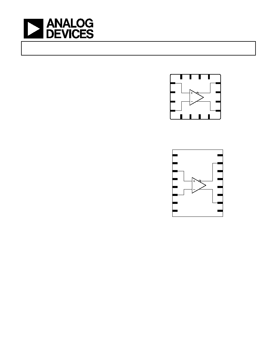
PIN CONFIGURATIONS
03600-0-001
+IN
DGND
NC = NO CONNECT
NC
NC
NC
NC
NC
I
ADJ
V
OCM
PWDN0
PWDN1
≠IN
≠OUT
V
EE
V
CC
+OUT
1
4
12
13
16
8
5
9
Figure 1. 4 mm ◊ 4 mm 16-Lead LFCSP
03600-0-002
V
OCM
NC
+IN
PWDN1
PWDN0
≠IN
NC
DGND
NC
NC = NO CONNECT
≠OUT
NC
V
EE
V
CC
NC
+OUT
I
ADJ
16
1
9
8
Figure 2. 16-Lead QSOP/EP
The low power consumption, high output current, high output
voltage swing, and robust thermal packaging enable the AD8390
to be used as the central office line driver in ADSL, ADSL2+,
and proprietary xDSL systems, as well as in other high current
applications requiring a differential amplifier.
Rev. C
Information furnished by Analog Devices is believed to be accurate and reliable.
However, no responsibility is assumed by Analog Devices for its use, nor for any
infringements of patents or other rights of third parties that may result from its use.
Specifications subject to change without notice. No license is granted by implication
or otherwise under any patent or patent rights of Analog Devices. Trademarks and
registered trademarks are the property of their respective owners.
One Technology Way, P.O. Box 9106, Norwood, MA 02062-9106, U.S.A.
Tel: 781.329.4700
www.analog.com
Fax: 781.326.8703
© 2004 Analog Devices, Inc. All rights reserved.

AD8390
Rev. C | Page 2 of 16
TABLE OF CONTENTS
Specifications..................................................................................... 3
Absolute Maximum Ratings............................................................ 5
Typical Thermal Properties............................................................. 5
ESD Caution.................................................................................. 5
Typical Performance Characteristics ............................................. 6
Theory of Operation ........................................................................ 9
Applications....................................................................................... 9
Circuit Definitions ....................................................................... 9
Analyzing a Basic Application Circuit....................................... 9
Setting the Closed-Loop Gain .................................................... 9
Calculating Input Impedance ..................................................... 9
Setting the Output Common-Mode Voltage .......................... 10
Power-Down Features and the I
ADJ
Pin ................................... 10
PWDN Pins............................................................................. 10
ADSL and ADSL2+ Applications ......................................... 10
ADSL and ADSL2+ Applications Circuit............................ 10
Multitone Power Ratio (MTPR)............................................... 11
Layout, Grounding, and Bypassing .......................................... 12
Power Dissipation and Thermal Management....................... 12
Outline Dimensions ....................................................................... 13
Ordering Guide .......................................................................... 13
REVISION HISTORY
9/04≠Data Sheet Changed from Rev. B to Rev. C
Change to Ordering Guide............................................................ 16
2/04≠Data Sheet Changed from Rev. A to Rev. B.
Changed pub code .......................................................................... 16
1/04≠Data sheet changed from Rev. Sp0f to Rev. A.
Added detailed description of product............................Universal
Updated Outline Dimensions ....................................................... 13

AD8390
Rev. C | Page 3 of 16
SPECIFICATIONS
V
S
= ±12 V or +24 V, R
L
= 100 , G = 10, PWDN = (1,1), I
ADJ
= NC, V
OCM
= float, T
A
= 25∞C, unless otherwise noted.
1, 2
Table 1.
Parameter Conditions
Min
Typ
Max
Unit
DYNAMIC PERFORMANCE
≠3 dB Small Signal Bandwidth
V
OUT
= 0.2 V p-p, R
F
= 10 k
40
60
MHz
Large Signal Bandwidth
V
OUT
= 4 V p-p
25
40
MHz
Peaking
V
OUT
= 0.2 V p-p
0.1
dB
Slew Rate
V
OUT
= 4 V p-p
300
V/µs
NOISE/DISTORTION PERFORMANCE
Second Harmonic Distortion
f
C
= 1 MHz, V
OUT
= 2 V
p-p
≠82 dBc
Third Harmonic Distortion
f
C
= 1 MHz, V
OUT
= 2 V
p-p
≠91 dBc
Multitone Power Ratio (26 kHz to 1.1 MHz)
Z
= 100 , P
= 19.8 dBm,
crest factor (CF) = 5.4
LINE
LINE
≠70
dBc
Multitone Power Ratio (26 kHz to 2.2 MHz)
Z
= 100 , P
= 19.8 dBm,
crest factor (CF) = 5.4
LINE
LINE
≠65 dBc
Voltage Noise (RTI)
f = 10 kHz
8
nV/Hz
Input Current Noise
f = 10 kHz
1
pA/Hz
INPUT CHARACTERISTICS
RTI Offset Voltage (V
OS,DM(RTI)
) V
+IN
≠ V
≠IN
, V
OCM
= midsupply
≠3.0
±1.0
+3.0
mV
RTI Offset Voltage (V
OS,DM(RTI)
) V
+IN
≠ V
≠IN
, V
OCM
= float
≠3.0
±1.0
+3.0
mV
±Input Bias Current
≠4.0
≠7.0
µA
Input Offset Current
≠0.35
±0.05
+0.35
µA
Input Resistance
400
k
Input Capacitance
2
pF
Common-Mode Rejection Ratio
(V
OS,DM(RTI)
)/(V
IN,CM
) 58
64
dB
OUTPUT CHARACTERISTICS
Differential Output Voltage Swing
V
OUT
43.8 44.2
44.6 V
Output Balance Error
(V
OS,CM
)/V
OUT
60 dB
Linear Output Current
R
L
= 10 , f
C
= 100 kHz
400
mA
Worst harmonic = ≠60 dBc
Output Common-Mode Offset
(V
+OUT
+ V
≠OUT
)/2, V
OCM
= midsupply
≠75
±35
+75
mV
Output Common-Mode Offset
(V
+OUT
+ V
≠OUT
)/2, V
OCM
= float
≠75
±35
+75
mV
POWER SUPPLY
Operating Range (Dual Supply)
±5
±12
V
Operating Range (Single Supply)
+10
+24
V
Total Quiescent Current
PWDN1, PWDN0 = (1,1); I
ADJ
= V
EE
5.2 6.5
mA
(1,0); I
ADJ
= V
EE
3.8 5.0
mA
(0,1); I
ADJ
= V
EE
2.5 3.5
mA
(0,0); I
ADJ
= V
EE
0.57 1.0
mA
Total Quiescent Current
PWDN1, PWDN0 = (1,1); I
ADJ
= NC
10.0
11.0
mA
(1,0); I
ADJ
= NC
6.7
8.0
mA
(0,1); I
ADJ
= NC
3.8
5.0
mA
(0,0); I
ADJ
= NC
0.67
1.0
mA
Power Supply Rejection Ratio (PSRR)
V
OS,DM
/V
S
, V
S
= ±1 V, V
OCM
= midsupply
70
76
dB
PWDN = 0 (Low Logic State)
1.0
V
PWDN = 1 (High Logic State)
1.6
V
V
OCM
TO ±V
OUT
SPECIFICATIONS
Input Voltage Range
≠11.0 to +10.0
V
Input Resistance
28
k
V
OCM
Accuracy
V
OUT,CM
/V
OCM
0.996 1.0
1.004 V/V
1
V
OCM
bypassed with 0.1 µF capacitor.
2
See
.
Figure 3

AD8390
Rev. C | Page 4 of 16
V
S
= ±5 V or +10 V, R
L
= 100 , G = 10, PWDN = (1,1), I
ADJ
= NC, V
OCM
= float, T
A
= 25∞C, unless otherwise noted.
1, 2
Table 2.
Parameter Conditions
Min
Typ
Max
Unit
DYNAMIC
PERFORMANCE
≠3 dB Small Signal Bandwidth
V
OUT
= 0.2 V p-p, R
F
= 10 k, G = 10
40 60
MHz
Large Signal Bandwidth
V
OUT
= 4 V p-p
25
40
MHz
Peaking
V
OUT
= 0.2 V p-p
0.1
dB
Slew Rate
V
OUT
= 4 V p-p
300
V/µs
NOISE/DISTORTION
PERFORMANCE
Second Harmonic Distortion
f
C
= 1 MHz, V
OUT
= 2 V p-p
≠82
dBc
Third Harmonic Distortion
f
C
= 1 MHz, V
OUT
= 2 V p-p
≠91 dBc
Voltage Noise (RTI)
f = 10 kHz
8
nV/Hz
Input Current Noise
f = 10 kHz
1
pA/Hz
INPUT
CHARACTERISTICS
RTI Offset Voltage (V
OS,DM(RTI)
) V
+IN
≠ V
≠IN
, V
OCM
= midsupply
≠3.0
±1.0
+3.0
mV
RTI Offset Voltage (V
OS,DM(RTI)
) V
+IN
≠ V
≠IN
, V
OCM
= float
≠3.0
±1.0
+3.0
mV
±Input Bias Current
≠4.0
≠7.0
µA
Input Offset Current
≠0.35
±0.05
+0.35
µA
Input
Resistance
400 k
Input Capacitance
2
pF
Common-Mode Rejection Ratio
(V
OS,DM(RTI)
)/(V
IN,CM
) 58
64
dB
OUTPUT
CHARACTERISTICS
Differential Output Voltage Swing
V
OUT
16.0 16.4
16.8 V
Output Balance Error
(V
OS,CM
)/V
OUT
60 dB
Linear Output Current
R
L
= 10 , f
C
= 100 kHz
400
mA
Worst harmonic = ≠60 dBc
Output Common-Mode Offset
(V
+OUT
+ V
≠OUT
)/2, V
OCM
= midsupply
≠75
±35 +75
mV
Output Common-Mode Offset
(V
+OUT
+ V
≠OUT
)/2, V
OCM
= float
≠75
±35 +75
mV
POWER
SUPPLY
Operating Range (Dual Supply)
±5
±12
V
Operating Range (Single Supply)
+10
+24
V
Total Quiescent Current
PWDN1, PWDN0 = (1,1); I
ADJ
= V
EE
4.5 5.5
mA
(1,0); I
ADJ
= V
EE
3.3 4.0
mA
(0,1); I
ADJ
= V
EE
2.1 3.0
mA
(0,0); I
ADJ
= V
EE
0.43 1.0
mA
Total Quiescent Current
PWDN1, PWDN0 = (1,1); I
ADJ
= NC
8.7
10.0
mA
(1,0); I
ADJ
= NC
5.8
7.0
mA
(0,1); I
ADJ
= NC
3.3
4.0
mA
(0,0); I
ADJ
= NC
0.55
1.0
mA
Power Supply Rejection Ratio
V
OS,DM
/V
S
, V
S
= ±1 V, V
OCM
= midsupply
70
76
dB
PWDN = 0 (Low Logic State)
1.0
V
PWDN = 1 (High Logic State)
1.6
V
V
OCM
TO ±V
OUT
SPECIFICATIONS
Input Voltage Range
≠4.0 to +3.0
V
Input
Resistance
28 k
V
OCM
Accuracy
V
OUT,CM
/V
OCM
0.996 1.0
1.004 V/V
1
V
OCM
bypassed with 0.1 µF capacitor.
2
See
.
Figure 3
AD8390
Rev. C | Page 5 of 16
ABSOLUTE MAXIMUM RATINGS
Table 3.
Parameter Rating
Supply Voltage
±13.2 V (26.4 V)
V
OCM
V
EE
< V
OCM
< V
CC
Package Power Dissipation
(T
J
MAX
≠ T
A
)/
JA
Maximum Junction Temperature (T
J
MAX
) 150∞C
Operating Temperature Range (T
A
)
≠40∞C to +85∞C
Storage Temperature Range
≠65∞C to +150∞C
Lead Temperature (Soldering 10 s)
300∞C
Stresses above those listed under Absolute Maximum Ratings
may cause permanent damage to the device. This is a stress
rating only; functional operation of the device at these or any
other conditions above those indicated in the operational
section of this specification is not implied. Exposure to absolute
maximum rating conditions for extended periods may affect
device reliability.
TYPICAL THERMAL PROPERTIES
Table 4.
Package
Typical Thermal Resistance (
JA
)
16-lead LFCSP (CP-16)
JEDEC 2S2P ≠ 0 airflow
Paddle soldered to board
Nine thermal vias in pad
30.4∞C/W
16-lead QSOP/EP (RC-16)
JEDEC 1S2P ≠ 0 airflow
Paddle soldered to board
Nine thermal vias in pad
44.3∞C/W
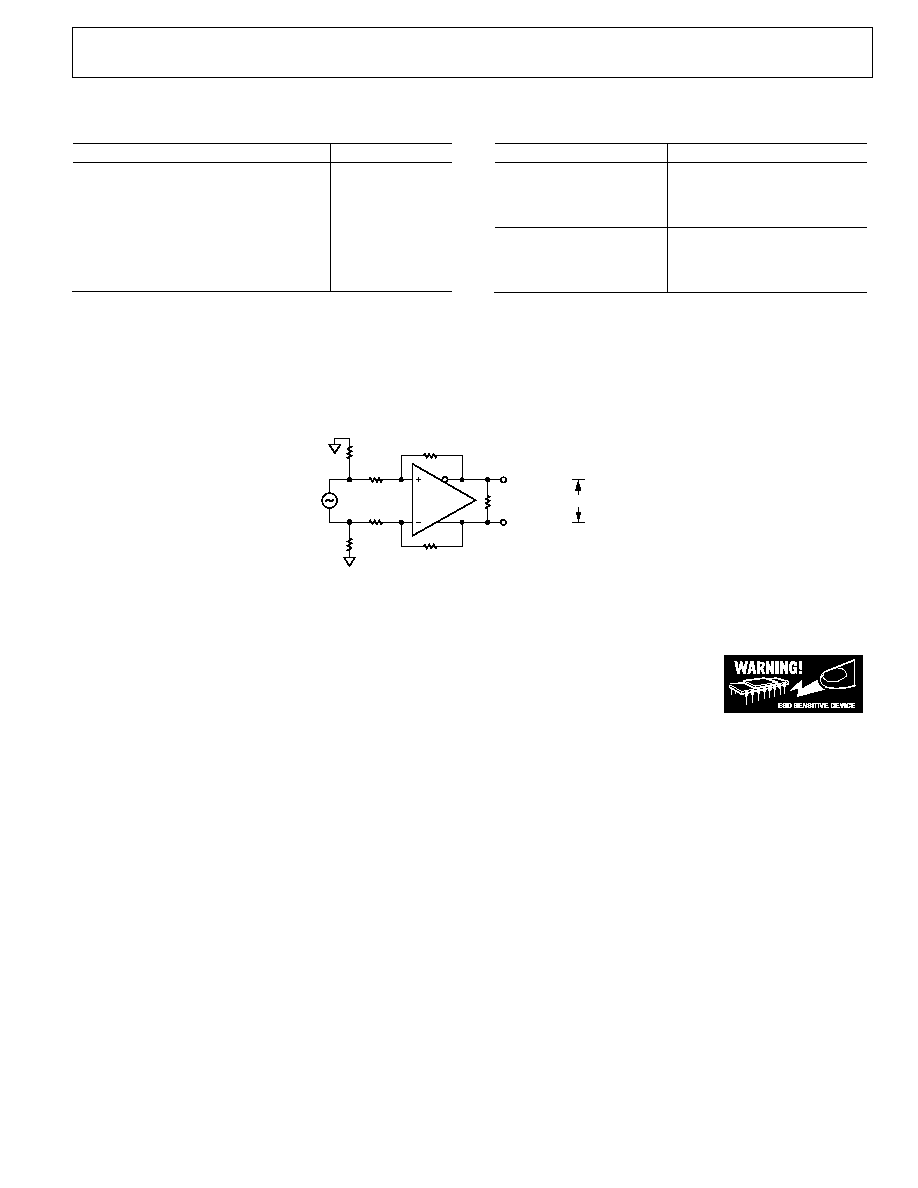
03600-0-003
R
F
= 10k
R
G
= 1k
49.9
49.9
R
G
= 1k
V
IN
R
L,DM
= 100
R
F
= 10k
AD8390
V
OUT,DM
Figure 3. Basic Test Circuit
ESD CAUTION
ESD (electrostatic discharge) sensitive device. Electrostatic charges as high as 4000 V readily accumulate on
the human body and test equipment and can discharge without detection. Although this product features
proprietary ESD protection circuitry, permanent damage may occur on devices subjected to high energy
electrostatic discharges. Therefore, proper ESD precautions are recommended to avoid performance
degradation or loss of functionality.
AD8390
Rev. C | Page 6 of 16
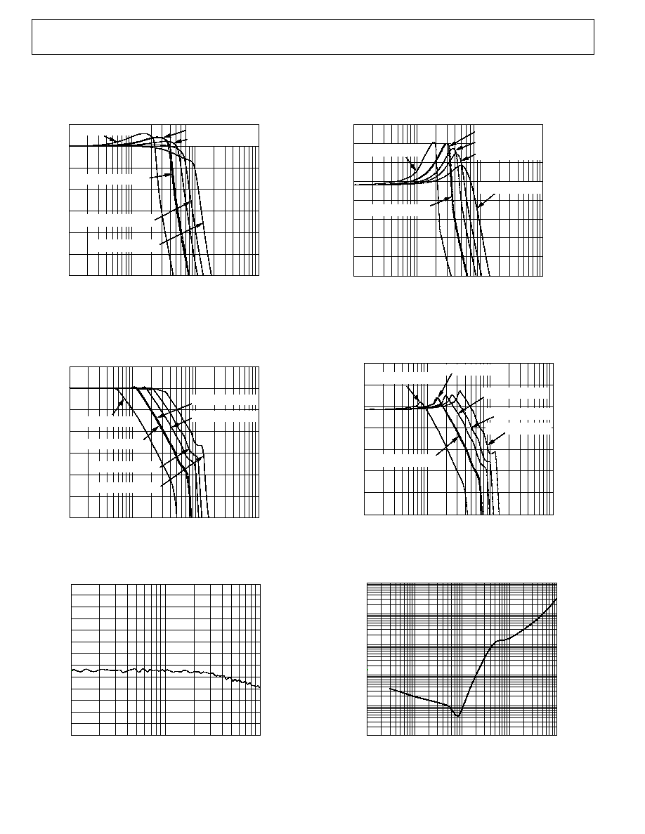
TYPICAL PERFORMANCE CHARACTERISTICS
Default Conditions: V
S
= ±12 V or +24 V, R
L
= 100 , G = 10, PWDN = (1,1), I
ADJ
= NC, V
OCM
= float (bypassed with 0.1 F capacitor),
T
A
= 25∞C, unless otherwise noted. See Figure 3.
25
20
15
10
GA
IN
(
d
B
)
5
0
≠5
≠10
1
10
100
1000
FREQUENCY (MHz)
PWDN(1,0); I
ADJ
= NC
PWDN(0,1); I
ADJ
= V
EE
PWDN(0,1); I
ADJ
= NC
PWDN(1,0); I
ADJ
= V
EE
PWDN(1,1); I
ADJ
= V
EE
PWDN(1,1); I
ADJ
= NC
03600-0-004
Figure 4. Small Signal Frequency Response;
V
S
= ±12 V, Gain = 10, V
OUT
= 200 mV p-p
25
20
15
10
GA
IN
(
d
B
)
5
0
≠5
≠10
1
10
100
1000
FREQUENCY (MHz)
PWDN(0,1); I
ADJ
= V
EE
PWDN(1,0); I
ADJ
= NC
PWDN(0,1); I
ADJ
= NC
PWDN(1,1); I
ADJ
= NC
PWDN(1,0); I
ADJ
= V
EE
PWDN(1,1); I
ADJ
= V
EE
03600-0-006
Figure 5. Large Signal Frequency Response;
V
S
= ±12 V, Gain = 10, V
OUT
= 4 V p-p
FE
E
D
THROUGH (dB)
≠75
≠70
≠65
≠60
≠55
≠50
≠45
≠40
≠35
≠30
≠25
≠20
≠15
≠10
1
10
100
FREQUENCY (MHz)
03600-0-008
Figure 6. Signal Feedthrough; PWDN = (0,0)
FREQUENCY (MHz)
30
25
20
15
10
GA
IN
(
d
B
)
5
0
≠5
≠10
1
10
100
1000
PWDN(1,0); I
ADJ
= V
EE
PWDN(1,1); I
ADJ
= V
EE
PWDN(1,0); I
ADJ
= NC
PWDN(0,1); I
ADJ
= V
EE
PWDN(1,1); I
ADJ
= NC
PWDN(0,1); I
ADJ
= NC
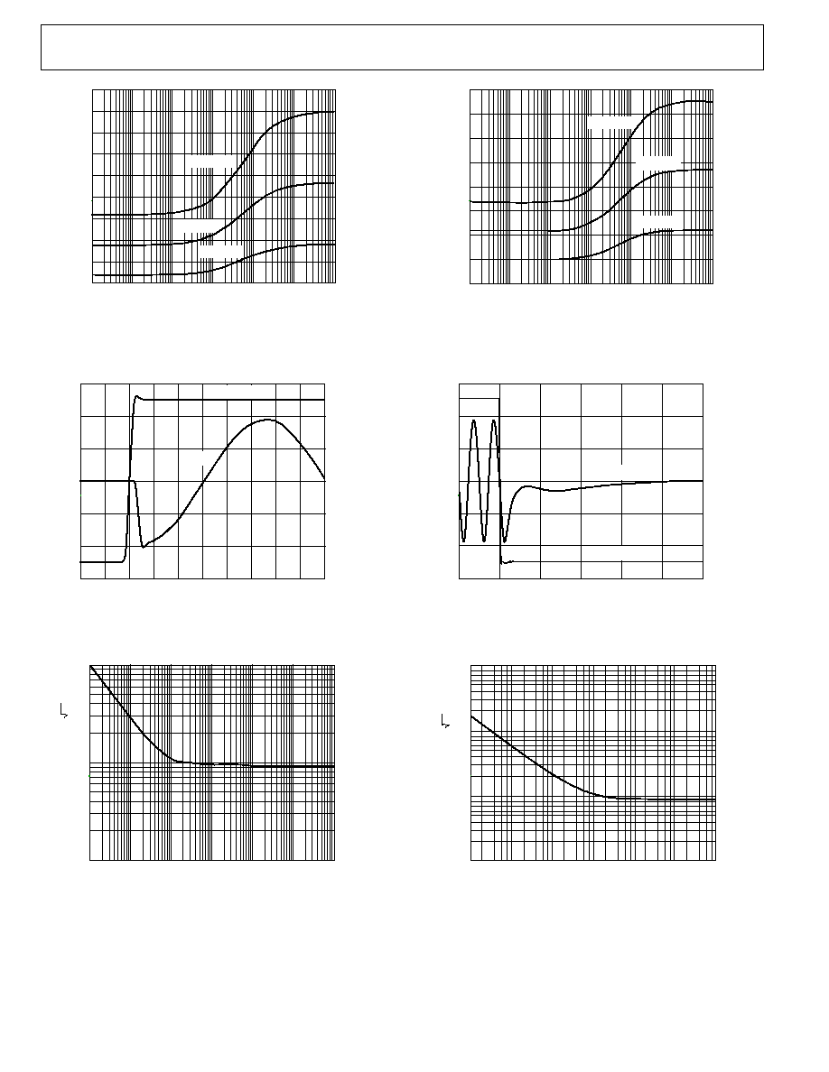
03600-0-026
Figure 7. Small Signal Frequency Response;
V
S
= ±5 V, Gain = 5, V
OUT
= 200 mV p-p
FREQUENCY (MHz)
03600-0-027
25
20
15
10
GA
IN
(
d
B
)
5
0
≠5
≠10
1
10
100
1000
PWDN(1,0); I
ADJ
= V
EE
PWDN(1,1); I
ADJ
= V
EE
PWDN(0,1); I
ADJ
= V
EE
PWDN(1,1); I
ADJ
= NC
PWDN(0,1); I
ADJ
= NC
PWDN(1,0); I
ADJ
= NC
Figure 8. Large Signal Frequency Response;
V
S
= ±5 V, Gain = 5, V
OUT
= 2 V p-p
FREQUENCY (MHz)
OUTP
UT I
M
P
E
DANCE
(
)
0.001
0.01
0.1
1
10
100
0.01
0.1
1
10
100
03600-0-020
Figure 9. Output Impedance vs. Frequency; PWDN = (1,1)
AD8390
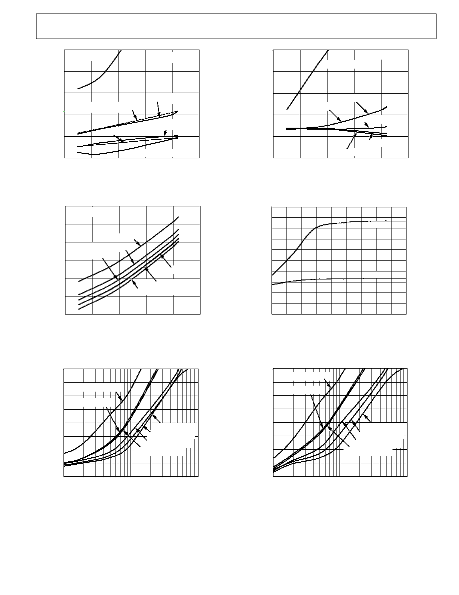
Rev. C | Page 7 of 16
OUTPUT POWER (dBm)
MULTITONE POW
E
R RATIO (dBc)
≠75
≠70
≠65
≠60
≠55
≠50
12
14
20
18
16
22
CREST FACTOR = 5.4
PWDN(1,0); I
ADJ
= NC
PWDN(0,1); I
ADJ
= NC
PWDN(1,1); I
ADJ
= NC
PWDN(1,0); I
ADJ
= V
EE
PWDN(1,1); I
ADJ
= V
EE
PWDN(0,1); I
ADJ
= V
EE
03600-0-010
Figure 10. MTPR vs. Output Power;
970 kHz Empty Bin (26 kHz to 1.1 MHz)
OUTPUT POWER (dBm)
03600-0-028
900
800
700
600
P
O
W
E
R CONS
UM
P
T
I
O
N (mW
)
500
400
300
12
16
14
18
20
22
PWDN(1,0); I
ADJ
= V
EE
PWDN(0,1); I
ADJ
= V
EE
PWDN(0,1); I
ADJ
= NC
PWDN(1,1); I
ADJ
= V
EE
PWDN(1,1); I
ADJ
= NC
PWDN(1,0); I
ADJ
= NC
CREST FACTOR = 5.4
Figure 11. Power Consumption vs. Output Power
(Includes Output Power Delivered to Load)
FREQUENCY (MHz)
03600-0-029
≠50
TOTAL HARMONI
C
DI
S
T
ORTI
ON (dBc
)
≠90
≠85
≠80
≠75
≠70
≠65
≠60
≠55
0.1
1
10
PWDN(1,1); I
ADJ
= V
EE
PWDN(1,1); I
ADJ
= NC
PWDN(0,1); I
ADJ
= V
EE
PWDN(0,1); I
ADJ
= NC
PWDN(1,0); I
ADJ
= V
EE
PWDN(1,0); I
ADJ
= NC
Figure 12. Total Harmonic Distortion vs. Frequency;
V
S
= ±12 V, V
OUT
= 2 V p-p
OUTPUT POWER (dBm)
03600-0-030
≠45
MULTITONE POW
E
R RATIO (dBc)
≠70
≠65
≠60
≠55
≠50
12
22
20
18
16
14
PWDN(0,1); I
ADJ
= V
EE
PWDN(0,1); I
ADJ
= NC
PWDN(1,0); I
ADJ
= V
EE
PWDN(1,1); I
ADJ
= V
EE
PWDN(1,1); I
ADJ
= NC
PWDN(1,0); I
ADJ
= NC
CREST FACTOR = 5.4
Figure 13. MTPR vs. Output Power;
1.75 MHz Empty Bin (26 kHz to 2.2 MHz)
R
LOAD
(
)
03600-0-031
50
DIFFE
RE
NTIAL OUTP
UT S
W
ING (V
)
0
45
40
35
30
25
20
15
10
5
10
20
30
40
50
60
70
80
90
100
V
S
=
±
12V
V
S
=
±
5V
Figure 14. Differential Output Swing vs. R
LOAD
FREQUENCY (MHz)
03600-0-032
≠50
TOTAL HARMONIC DIS
T
ORTION (dBc
)
≠90
≠85
≠80
≠75
≠70
≠65
≠60
≠55
0.1
1
10
PWDN(1,1); I
ADJ
= V
EE
PWDN(1,1); I
ADJ
= NC
PWDN(0,1); I
ADJ
= V
EE
PWDN(0,1); I
ADJ
= NC
PWDN(1,0); I
ADJ
= V
EE
PWDN(1,0); I
ADJ
= NC
Figure 15. Total Harmonic Distortion vs. Frequency;
V
S
= ±5 V, V
OUT
= 2 V p-p
AD8390
Rev. C | Page 8 of 16
I
ADJ
SERIES RESISTOR (
)
S
U
P
P
L
Y
CURRE
NT (mA)
2
3
4
5
6
7
8
9
10
11
1
10
100
1k
10k
100k
1M
PWDN(1,1)
PWDN(0,1)
PWDN(1,0)
03600-0-016
Figure 16. Quiescent Current vs. I
ADJ
Resistor; V
S
= ±12 V
TIME (
µ
s)
DI
FFE
RE
NTI
A
L OUTP
UT (V
)
PWD
N
PIN
VA
LU
ES (
V
)
≠3
≠2
≠1
0
1
2
3
≠0.5
0.5
1.5
2.5
3.5
4.5
5.5
≠0.2 ≠0.1
0
0.1
0.2
0.3
0.4
0.5
0.6
0.7
0.8
OUTPUT
PWDN PINS
03600-0-018
Figure 17. Power-Up Time;
PWDN = (0,0) to PWDN = (1,1)
FREQUENCY (Hz)
VOLTA
GE N
O
ISE (
n
V/
1
10
100
10
100
100k
1M
10k
1k
10M
03600-0-014
Hz)
Figure 18. Voltage Noise (RTI)
I
ADJ
SERIES RESISTOR (
)
S
U
P
P
L
Y
CURRE
NT (mA)
2
1
3
4
5
6
7
8
9
1
10
100
1k
10k
100k
1M
PWDN(1,1)
PWDN(0,1)
PWDN(1,0)
03600-0-017
Figure 19. Quiescent Current vs. I
ADJ
Resistor; V
S
= ±5 V
TIME (
µ
s)
DIFFE
RE
NTIAL OUTP
UT (V
)
PWD
N
PIN
VA
LU
ES (
V
)
≠3
≠2
≠1
0
1
2
3
≠0.5
0.5
1.5
2.5
3.5
4.5
5.5
≠2
0
2
4
6
8
10
OUTPUT
PWDN PINS
03600-0-019
Figure 20. Power-Down Time;
PWDN = (1,1) to PWDN = (0,0)
FREQUENCY (Hz)
CURRE
NT NOI
S
E
(pA/
Hz)
0.1
1.0
10
100
10
100
1k
10k
100k
1M
10M
03600-0-015
Figure 21. Current Noise (RTI)
AD8390
Rev. C | Page 9 of 16
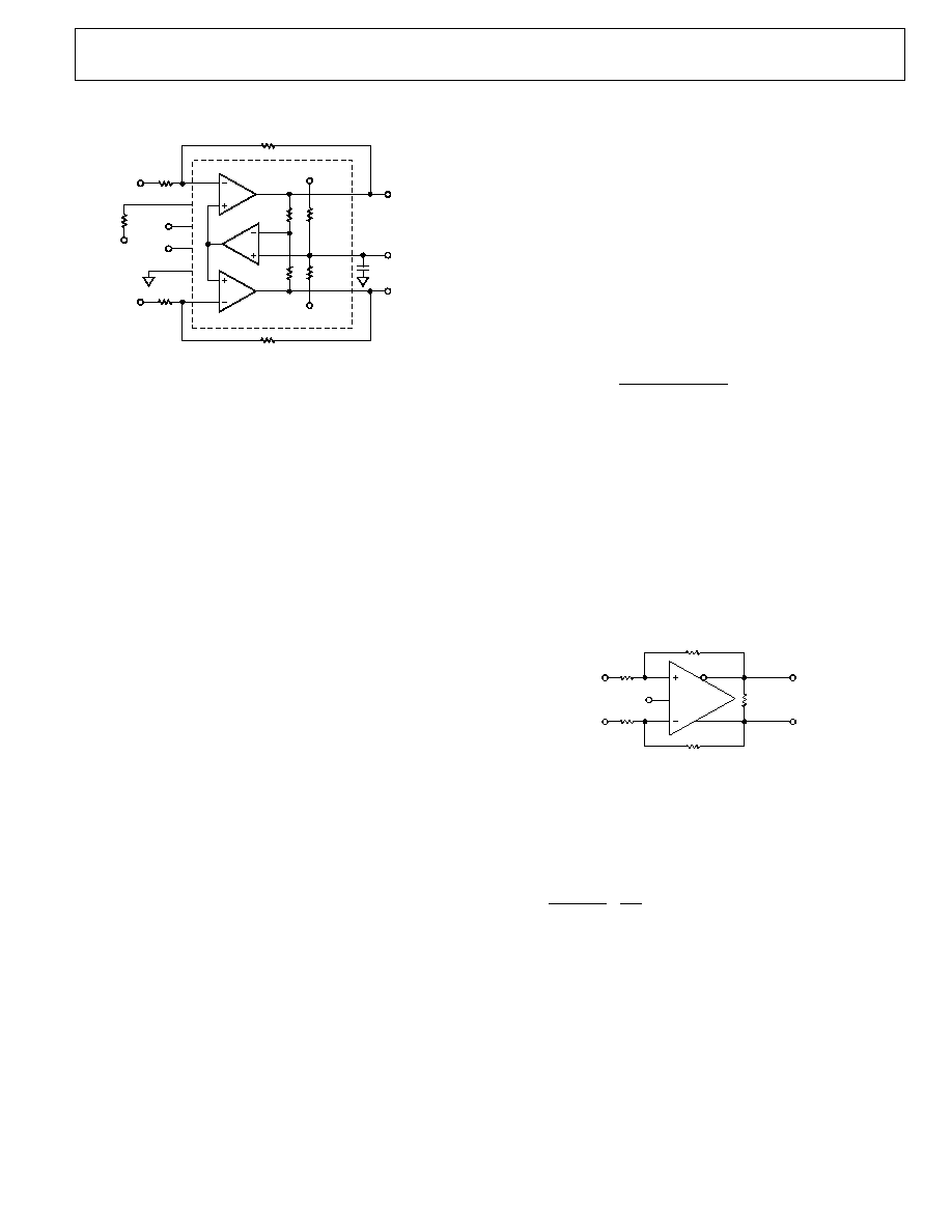
THEORY OF OPERATION
03600-0-035
A
C
B
50k
R
G
R
G
50k
56k
V
CC
56k
V
OCM
BYP
+OUT
AD8390
≠OUT
+IN
I
ADJ
PWDN0
R
ADJ
PWDN1
DGND
≠IN
V
EE
V
EE
R
F
R
F
Figure 22. Functional Block Diagram
The AD8390 is a true differential operational amplifier with
common-mode feedback. The AD8390 is functionally equivalent
to three op amps, as shown in Figure 22. Amplifiers A and B act
like a standard dual op amp in an inverting configuration that
requires four resistors to set the desired gain.
The third amplifier (C) maintains the common-mode voltage
(V
OCM
) at the output of the AD8390. V
OCM
is internally
generated, as shown in Figure 22. The common-mode feedback
amplifier (C) drives the noninverting terminals of A and B such
that the difference between the output common-mode voltage
and V
OCM
is always zero. This functionality forces the outputs to
sit at midsupply, which results in differential outputs of identical
amplitude and 180 degrees out of phase. The user also has the
option to externally drive the V
OCM
pin as an input to set the dc
output common-mode voltage. For details, see the Setting the
Output Common-Mode Voltage section.
APPLICATIONS
CIRCUIT DEFINITIONS
Differential voltage refers to the difference between two node
voltages. For example, the output differential voltage (or output
differential-mode voltage) is defined as
(
)
OUT
OUT
DM
OUT
V
V
V
-
+
-
=
,
(1)
V
+OUT
and V
≠OUT
refer to the voltages at the +OUT and ≠OUT
terminals with respect to a common reference.
Common-mode voltage refers to the average of the two node
voltages. The output common-mode voltage is defined as
(
)
2
,
OUT
OUT
CM
OUT
V
V
V
-
+
+
=
(2)
ANALYZING A BASIC APPLICATION CIRCUIT
The AD8390 uses high open-loop gain and negative feedback to
force its differential and common-mode output voltages in such
a way as to minimize the differential and common-mode error
voltages. The differential error voltage is defined as the voltage
between the differential inputs +IN and ≠IN, as shown in
Figure 23. For most purposes, this voltage can be assumed to be
zero. Similarly, the difference between the actual output
common-mode voltage and the voltage applied to V
OCM
can also
be assumed to be zero. Starting from these two assumptions, any
application circuit can be analyzed.
03600-0-022
R
F
≠OUT
+OUT
+IN
≠IN
R
G
V
OCM
R
G
R
L,DM
V
OUT,DM
+
≠
V
IN,DM
≠
+
R
F
Figure 23. Basic Applications Circuit
(I
ADJ
Pin Not Connected, and PWDN0 and PWDN1 Held High)
SETTING THE CLOSED-LOOP GAIN
The differential-mode gain of the circuit in Figure 23 can be
described by
G
F
DM
IN
DM
OUT
R
R
V
V
=
,
,
(3)
CALCULATING INPUT IMPEDANCE
The input impedance of the circuit in Figure 23 between the
inputs (V
+IN
and V
-IN
) is simply
G
DM
IN
R
R
◊
= 2
,
(4)
AD8390
Rev. C | Page 10 of 16
SETTING THE OUTPUT COMMON-MODE VOLTAGE
By design, the AD8390's V
OCM
pin is internally biased at a
voltage equal to the midsupply point (average value of the
voltages on V
CC
and V
EE
), eliminating the need for external
resistors. The high impedance nature of the V
OCM
pin, however,
allows the designer to force it to a desired level with an external
low impedance source. It should be noted that the V
OCM
pin is
not intended for use as an ac signal input.
The three configurations for the V
OCM
pin are floating with a
single supply, floating with dual supplies, and forcing the pin
with an external source. If not externally forcing the V
OCM
pin,
the designer must decouple it to ground with a 0.1 µF capacitor
in close proximity to the AD8390.
With dual equal supplies (for example, ±12 V) such that the
midpoint of the supplies is nominally 0 V, the user may opt to
connect the V
OCM
pin directly to ground, thus eliminating the
need for an external decoupling capacitor.
POWER-DOWN FEATURES AND THE I
ADJ
PIN
The AD8390 offers significant versatility in setting quiescent
bias levels for a particular application from full ON to full OFF.
This versatility gives the circuit designer the flexibility to maxi-
mize efficiency while maintaining optimal levels of performance.
Optimizing driver efficiency while delivering the required signal
level is accomplished with the AD8390 through the use of two
on-chip power management features: two PWDN pins used to
select one of four bias modes, and an I
ADJ
pin used for additional
power management including fine bias adjustments.
PWDN Pins
Two digitally programmable logic pins, PWDN1 and PWDN0,
may be used to select four different bias levels (see Table 5).
These levels start with full power if the I
ADJ
pin is not connected.
The top bias level can also start at approximately half of full bias,
if the I
ADJ
pin is connected to V
EE
or to ground in a single-supply
configuration, R
ADJ
= 0. The bias level can be controlled with
CMOS logic levels (high = 1) applied to the PWDN1 and PWDN0
pins alone or in combination with the I
ADJ
control pin. The
digital ground pin (DGND) is the logic ground reference for the
PWDN1 and PWDN0 pins. PWDN = (0,0) is the power-down
mode of the amplifier.
The AD8390 exhibits a low output impedance for PWDN1,0 =
(1,1), (1,0), and (0,1). At PWDN1,0 = (0,0), however, the output
impedance is undefined. The lowest power mode (0,0) of the
AD8390 alone may not be suitable for systems that rely on a
high impedance OFF state, such as multiplexing.
I
ADJ
Pin
The I
ADJ
feature offers users significant flexibility in setting the
bias level of the AD8390 by allowing for fine tuning of the bias
setting. Use of the I
ADJ
feature is not required for operation of
the AD8390.
When I
ADJ
is not connected, the bias current in the various
power modes is set to approximately 10 mA, 6.7 mA, and
3.8 mA for power modes PWDN1,0 = (1,1), (1,0), and (0,1),
respectively, as seen in Table 5. Setting I
ADJ
= V
EE
for dual-supply
operation (or grounding the I
ADJ
pin for single-supply opera-
tion) cuts the bias setting approximately in half for each mode.
A resistor (R
ADJ
) between I
ADJ
and ground for single-supply
operation, or I
ADJ
and V
EE
for dual-supply operation, allows fine
bias adjustment between the bias levels preset by the PWDN
pins. Figure 16 and Figure 19 depict the effect of different R
ADJ
values on setting the bias levels.
Table 5. PWDN Code Selection Guide
PWDN1 PWDN0 R
ADJ
(
)
I
Q
(mA)
1 1
10.0
1 0
6.7
0 1
3.8
0 0
0.67
1 1 0
5.2
1 0 0
3.8
0 1 0
2.5
0 0 0
0.57
ADSL and ADSL2+ Applications
The AD8390 line driver amplifier is an efficient class AB amplifier
that is ideal for driving xDSL signals. The AD8390 may be used
for driving ADSL or ADSL2+ modulated signals in either direc-
tion: upstream from CPE to the CO or downstream from the
CO to CPE.
ADSL and ADSL2+ Applications Circuit
Increased CO port density has made driver power efficiency an
important requirement in ADSL and ADSL2+ systems. The lar-
gest impact on efficiency is due to the need for back termina-
tion of the driver. In the simplest case, this is accomplished with
a pair of resistors, each equal to half the reflected line impedance,
in series with the outputs of the differential driver. In this scen-
ario, half the transmitted power is consumed by the back term-
ination resistors. This results in the need for higher turns ratio
transformers, which attenuate the receive signal and tend to be
more lossy. They also increase current requirements of the dri-
ver, effectively reducing headroom because the output devices
can no longer swing as close to the rail.
To solve this problem, it is common practice to use a combination
of negative and positive feedback to synthesize the output impe-
dance, thus decreasing the required ohmic value of the back
termination. Overall efficiency is improved because less power
is wasted in the back termination and a lower turns ratio trans-
former can be used without the need for increased supply rails.
The application circuit in Figure 24 depicts such an approach,
where the positive feedback, negative feedback, and back termi-
nation are provided by R2, R3, and R
M
, respectively.
AD8390
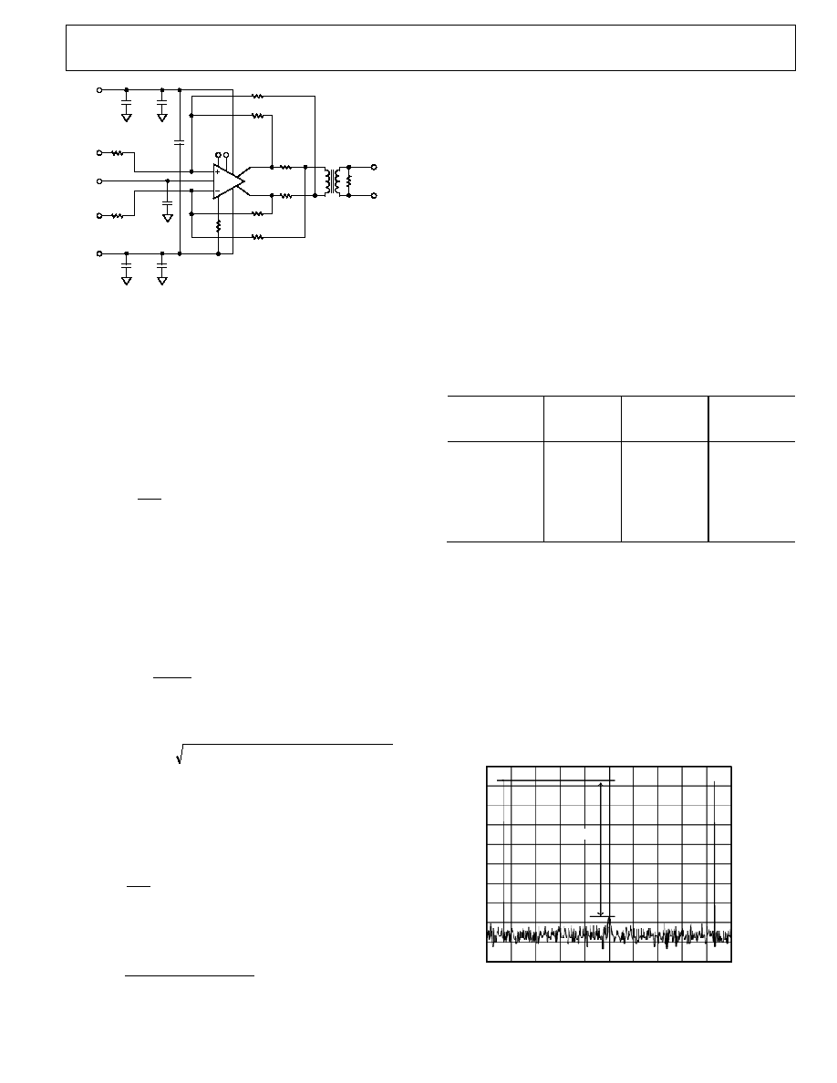
Rev. C | Page 11 of 16
03600-
0
-
036
P
W
DN1
P
W
DN0
R
M
R
L
V
OUT,DM
+
≠
≠OUT
+OUT
R
M
R3
R2
R1
R1
R3
0.1
µ
F
I
ADJ
R
ADJ
R2
1:N
10
µ
F
0.1
µ
F
V
CC
+IN
V
OCM
≠IN
10
µ
F
0.1
µ
F
0.1
µ
F
V
EE
Figure 24. ADSL/ADSL2+ Application Circuit
Referring to Figure 24, the following describes how to calculate
the resistor values necessary to obtain the desired input imped-
ance, gain, and output impedance.
The differential input impedance to the circuit is simply 2R1.
As such, R1 is chosen by the designer to yield the desired input
impedance.
When synthesizing the output impedance, a factor k is
introduced, which is used to express the ratio of the negative
feedback resistor to the positive feedback resistor by
R2
R3
k =
-
1
(5)
Along with the turns ratio N, k is also used to define the value of
the back termination resistors R
M
. Commonly used values for k
are 0.1 to 0.25. A k value of 0.1 would result in back termination
resistors that are only 1/10 as large as those in the simplest case
described above. Lower values of k result in greater amounts of
positive feedback. Therefore, values much lower than 0.1 can
lead to instability and are generally not recommended.
2
2 N
R
k
R
L
M
◊
◊
=
(6)
This factor (k), along with R1, R
M
, and the desired gain (A
V
), is
then used to calculate the necessary values for R3 and R2.
(
)
M
M
V
V
V
R
k
R
k
R1
A
R1
A
k
R1
A
R3
◊
-
+
◊
◊
◊
◊
+
◊
◊
=
2
(7)
The usually small value for R
M
allows a simplified approximation
for R3.
V
A
k
R1
R3
◊
◊
◊
2
(8)
k
R3
R2
-
=
1
(9)
Once R
M
, R3, and R2 are computed, the closest 1% resistors can
be chosen and the gain rechecked with the following equation:
(
)
R1
R3
R2
R2
k
R
R3
R2
A
M
V
◊
-
+
◊
+
◊
=
(10)
Table 6 shows a comparison of the results using the exact values,
the simplified approximation, and the closest 1% resistor values.
In this example, R1, A
V
, and k were chosen to be 1.0 k, 10 k,
and 0.1 k, respectively.
It should be noted that decreasing the value of the back termi-
nation resistors attenuates the receive signal by approximately
1/k. However, advances in low noise receive amplifiers permit
k values as small as 0.1 to be commonly used.
The line impedance, turns ratio, and k factor specify the output
voltage and current requirements from the AD8390. To accom-
modate higher crest factors or lower supply rails, the turns ratio,
N, may have to be increased. Since higher turns ratios and smaller
k factors both attenuate the receive signal, a large increase in N
may require an increase in k to maintain the desired noise
performance. Any particular design process requires that these
trade-offs be visited.
Table 6. Resistor Selection
Component
Exact
Values
Approximate
Calculation
Standard 1%
Resistor
Values
R1 ()
1000
1000
1000
R2 ()
2246.95
2222.22
2210
R3 ()
2022.25
2000
2000
R
M
()
5
5
4.99
Actual A
V
10.000 9.889
10.138
Actual k (Eq. 5)
0.1
0.1
0.095
MULTITONE POWER RATIO (MTPR)
Multitone power ratio is a commonly used figure of merit that
xDSL designers use to help describe system performance.
MTPR is the measured delta between the peak of a filled
frequency bin and the harmonic products that appear in an
intentionally empty frequency bin. Figure 25 illustrates this
principle. The plots in Figure 10 and Figure 13 show MTPR
performance in various power modes. All data were taken with
a circuit with a k factor of 0.1, a 1:1 turns ratio transformer, and
a waveform with a 5.4 peak-to-average ratio, also known as the
crest factor (CF).
03600-0-033
≠70dBc
10dB/DIV
CENTER 431.25kHz
SPAN 10kHz
1kHz/DIV
Figure 25. MTPR Measurement
AD8390
Rev. C | Page 12 of 16
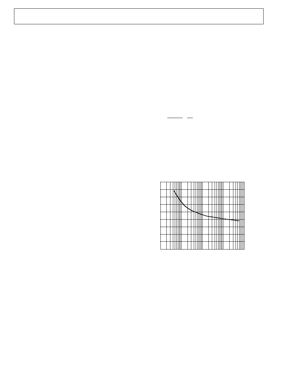
To obtain optimum thermal performance from the AD8390 in
either package, it is essential that the thermal pad be soldered to
a ground plane with minimal thermal resistance. This is par-
ticularly true for dense circuit designs with multiple integrated
circuits. Furthermore, the PCB should be designed in such a
manner as to draw the heat away from the ICs. Figure 26
illustrates the relationship between thermal resistance (∞C/W)
and the copper area (mm
2
) for the AD8390ACP soldered down
to a 4-layer board with a given copper area.
LAYOUT, GROUNDING, AND BYPASSING
The first layout requirement is for a good solid ground plane
that covers as much of the board area around the AD8390 as
possible. The only exception to this is that the two input pins
should be kept a few millimeters from the ground plane, and
ground should be removed from inner layers and the opposite
side of the board under the input traces. This minimizes the
stray capacitance on these nodes and helps preserve the gain
flatness versus frequency.
Figure 26 can be used to help determine the copper board area
required for proper thermal management of the AD8390. The
power dissipation of the AD8390 can be computed using
Equation 11. This number can then be inserted into the
following equation to yield the required
JA
:
The power supply pins should be bypassed as close as possible
to the device on a ground plane common with signal ground.
Good high frequency, ceramic chip capacitors should be used.
This bypassing should be done with a capacitance value of
0.01 F to 0.1 F for each supply. Low frequency bypassing
should be provided with 10 F tantalum capacitors from each
supply to signal ground. The signal routing should be short and
direct to avoid parasitic effects, particularly on traces connected
to the amplifier inputs. Wherever there are complementary
signals, a symmetrical layout should be provided to the extent
possible to maximize the balance performance. When running
differential signals over a long distance, the traces on the PCB
should be close together.
W
C
P
T
AD8390
RISE
JA
∞
=
=
(12)
where T
RISE
is the delta from the maximum expected ambient
temperature to the highest allowable die temperature. It is
generally recommended that the maximum die temperature be
limited to 125∞C, and in no case should it be allowed to exceed
150∞C.
POWER DISSIPATION AND THERMAL
MANAGEMENT
Using the
JA
computed in Equation 12, Figure 26 can be used to
determine the minimum copper area required for proper thermal
dissipation of the AD8390.
The AD8390 was designed to be the most efficient class AB
ADSL/ADSL2+ line driver available. Figure 11 shows the total
power consumption (delivered line power and power consumed)
of the AD8390 driving ADSL signals at varying output powers
and power modes. To accurately determine the amount of
power dissipated by the AD8390, it is necessary to subtract the
power delivered to the load, matching losses, and transformer
losses as follows:
Cu AREA (mm
2)
03600-0-034
90
JA
(∞
C
/
W)
0
20
10
30
40
50
60
70
80
1
100
1000
10
10000
mW
losses
mW
load
supply,mW
AD8390
P
P
P
P
,
,
-
-
=
(11)
where:
P
supply,mW
is the total supply power in mW drawn by the AD8390.
P
load,mW
is the power delivered into a 100 twisted-pair line in mW.
P
losses,mW
is the power dissipated by the matching resistors and
the transformer in mW.
Figure 26. Thermal Resistance vs. Copper Area
While this discussion focuses mainly on ADSL applications, the
same premise can be applied to determining the power dissipa-
tion of the AD8390 in any application.
AD8390
Rev. C | Page 13 of 16
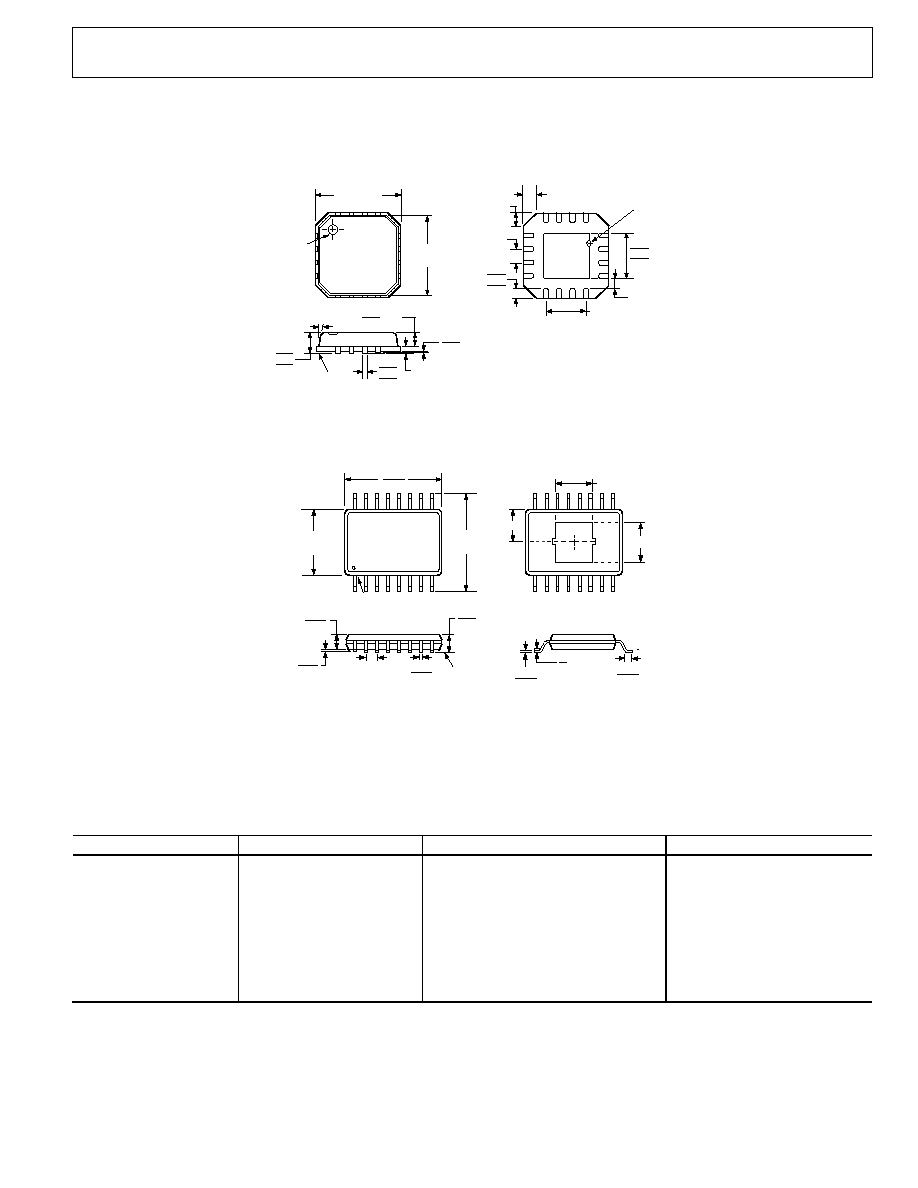
OUTLINE DIMENSIONS
16
5
13
8
9
12
1
4
BOTTOM
VIEW
2.25
2.10 SQ
1.95
0.75
0.60
0.50
0.65 BSC
1.95 BSC
0.35
0.28
0.25
12∞ MAX
0.20 REF
SEATING
PLANE
PIN 1
INDICATOR
TOP
VIEW
4.0
BSC SQ
3.75
BSC SQ
0.60 MAX
0.60 MAX
0.05 MAX
0.02 NOM
0.80 MAX
0.65 TYP
PIN 1
INDICATOR
1.00
0.85
0.80
COPLANARITY
0.08
0.25 MIN
COMPLIANT TO JEDEC STANDARDS MO-220-VGGC
Figure 27. 4 ◊ 4 mm 16-Lead Lead Frame Chip Scale Package [LFCSP]
(CP-16)
Dimensions shown in millimeters
16
9
8
1
0.197
0.189
0.236
BSC
PIN 1
0.154
BSC
SEATING
PLANE
0.010
0.004
0.012
0.008
0.025
BSC
0.010
0.006
0.050
0.016
COPLANARITY
0.004
0.065
0.049
0.069
0.053
BOTTOM VIEW
0.090
0.096
TOP VIEW
COMPLIANT TO JEDEC STANDARDS MO-137
8∞
0∞
0.077
Figure 28. 16-Lead Shrink Small Outline Package, Exposed Pad [QSOP/EP]
(RC-16)
Dimensions shown in inches
ORDERING GUIDE
Model
Temperature Range
Package Description
Package Option
AD8390ACP-R2
≠40∞C to +85∞C
16-Lead LFCSP
CP-16, 250 Piece Reel
AD8390ACP-REEL
≠40∞C to +85∞C
16-Lead LFCSP
CP-16, 13" Tape and Reel
AD8390ACP-REEL7
≠40∞C to +85∞C
16-Lead LFCSP
CP-16, 7" Tape and Reel
AD8390ACP-EVAL
Evaluation
Board
LFCSP
AD8390ARC
≠40∞C to +85∞C
16-Lead QSOP/EP
RC-16
AD8390ARC-REEL
≠40∞C to +85∞C
16-Lead QSOP/EP
RC-16, 13" Tape and Reel
AD8390ARC-REEL7
≠40∞C to +85∞C
16-Lead QSOP/EP
RC-16, 7" Tape and Reel
AD8390ARC-EVAL
Evaluation
Board
QSOP/EP

AD8390
Rev. C | Page 14 of 16
NOTES

AD8390
Rev. C | Page 15 of 16
NOTES

AD8390
Rev. C | Page 16 of 16
NOTES
© 2004 Analog Devices, Inc. All rights reserved. Trademarks and
registered trademarks are the property of their respective owners.
C02694≠0≠9/04(C)