AD8538 Low Power, Precision Auto-Zero Op Amp Data Sheet (REV.0)
Low Power, Precision Auto-Zero Op Amp
AD8538
Rev. 0
Information furnished by Analog Devices is believed to be accurate and reliable. However, no
responsibility is assumed by Analog Devices for its use, nor for any infringements of patents or other
rights of third parties that may result from its use. Specifications subject to change without notice. No
license is granted by implication or otherwise under any patent or patent rights of Analog Devices.
Trademarks and registered trademarks are the property of their respective owners.
One Technology Way, P.O. Box 9106, Norwood, MA 02062-9106, U.S.A.
Tel: 781.329.4700
www.analog.com
Fax: 781.461.3113
© 2005 Analog Devices, Inc. All rights reserved.
FEATURES
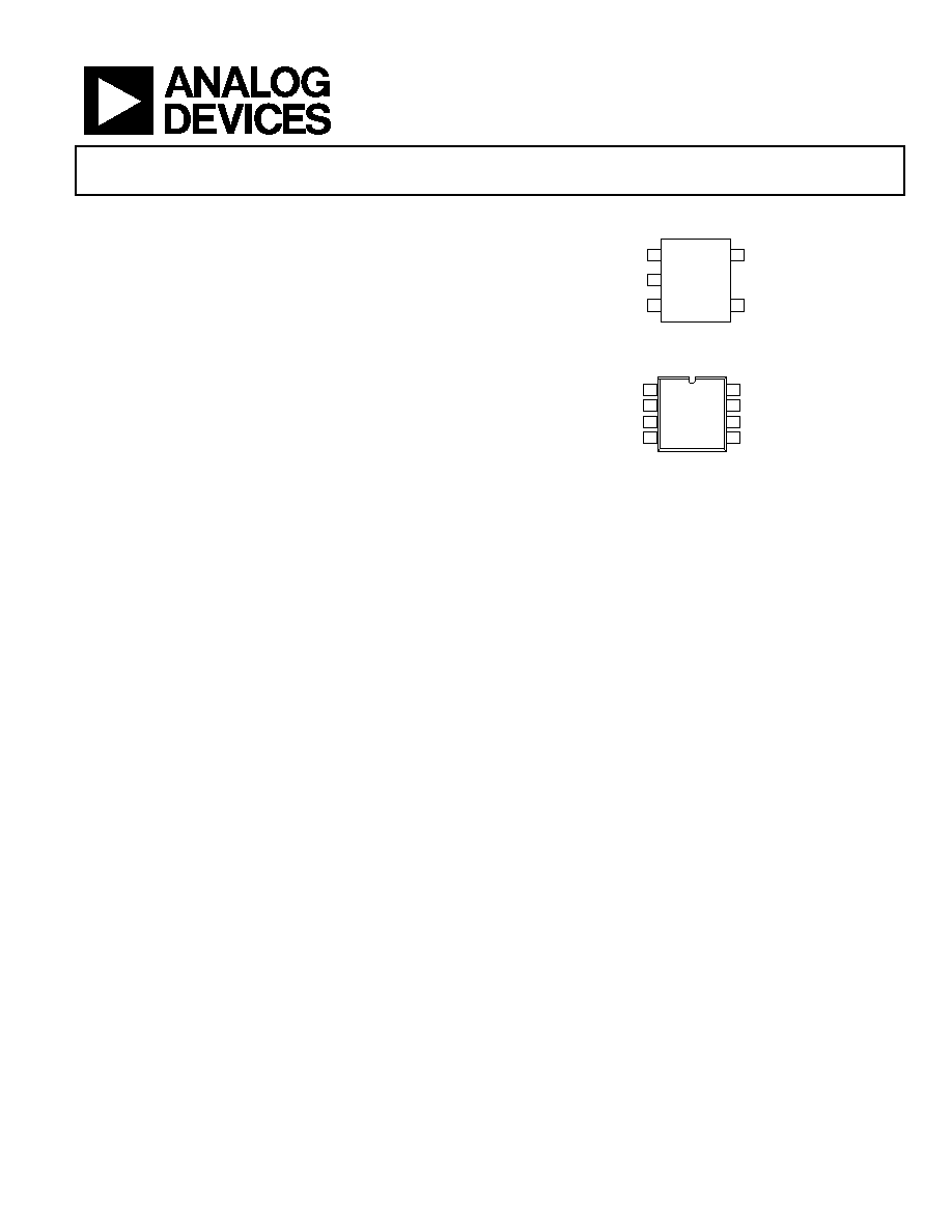
PIN CONFIGURATION DIAGRAMS
Low offset voltage: 13 V maximum
OUT
1
V
2
+IN
3
V+
5
IN
4
AD8538
TOP VIEW
(Not to Scale)
05
62
4-
00
2
Input offset drift: 0.03 V/°C
Single-supply operation: 2.7 V to 5.5 V
High gain, CMRR, and PSRR
Low input bias current: 25 pA
Figure 1. 5-Lead TSOT-23 (UJ-5)
Low supply current: 180 A
APPLICATIONS
NC
1
-IN
2
+IN
3
V-
4
NC
8
V+
7
OUT
6
NC
5
NC = NO CONNECT
AD8538
TOP VIEW
(Not to Scale)
05
62
4-
00
1
Mobile communications
Portable instrumentation
Battery-powered devices
Sensor interfaces
Temperature measurement
Electronic scales
Figure 2. 8-Lead SOIC_N (R-8)
GENERAL DESCRIPTION
The AD8538 is a very high precision amplifier featuring
extremely low offset voltage, low input bias current, and low
power consumption. The supply current is less than 180 A at
5.0 V. Operation is fully specified from 2.7 V to 5.0 V single
supply (±1.35 V to ±2.5 V dual supply).
The AD8538 operates using very low power making this
amplifier ideal for battery-powered devices and portable
equipment.
The AD8538 is specified over the extended industrial temperature
range (-40°C to +125°C). The AD8538 amplifier is available in
5-lead TSOT-23, and 8-lead, narrow body SOIC packages.

AD8538
Rev. 0 | Page 2 of 12
TABLE OF CONTENTS
Features .............................................................................................. 1
Applications....................................................................................... 1
Pin Configuration Diagrams........................................................... 1
General Description ......................................................................... 1
Revision History ............................................................................... 2
Specifications..................................................................................... 3
Electrical Specifications............................................................... 3
Absolute Maximum Ratings ............................................................5
Thermal Resistance .......................................................................5
ESD Caution...................................................................................5
Typical Performance Characteristics ..............................................6
Outline Dimensions ....................................................................... 12
Ordering Guide .......................................................................... 12
REVISION HISTORY
10/05--Revision 0: Initial Version

AD8538
Rev. 0 | Page 3 of 12
SPECIFICATIONS
ELECTRICAL SPECIFICATIONS
@V
S
= 5.0 V, V
CM
= 2.5 V, V
O
= 2.5 V, T
A
= 25°C, unless otherwise specified.
Table 1.
Parameter Symbol
Conditions
Min
Typ
Max
Unit
INPUT CHARACTERISTICS
Offset Voltage
V
OS
5
13
V
-40°C
T
A
+125°C
30
V
Input Bias Current
I
B
15
25
pA
-40°C
T
A
+85°C
35
100
pA
-40°C
T
A
+125°C
0.7
1.0
nA
Input Offset Current
I
OS
20
50
pA
-40°C
T
A
+125°C
150
pA
Input Voltage Range
0
5
V
Common-Mode Rejection Ratio
CMRR
V
CM
= 0 V to 5 V
115
150
dB
-40°C
T
A
+125°C; V
CM
= 0.2 V to 4.8 V
100
135
dB
Large Signal Voltage Gain
A
VO
R
L
= 10 k, V
O
= 0.1 V to 4.9 V
115
141
dB
-40°C
T
A
+125°C
110
135
dB
Offset Voltage Drift
V
OS
/
T -40°C T
A
+125°C
0.03
0.1
V/°C
OUTPUT CHARACTERISTICS
Output Voltage High
V
OH
R
L
= 100 k to ground
4.99
4.998
V
-40°C
T
A
+125°C
4.98
V
R
L
= 10 k to ground
4.95
4.970
V
-40°C
T
A
+125°C
4.94
V
Output Voltage Low
V
OL
R
L
= 100 k to V+
1.9
5
mV
-40°C
T
A
+125°C
2.8
7
mV
R
L
= 10 k to V+
17
20
mV
-40°C
T
A
+125°C
20
30
mV
Short-Circuit Limit
I
SC
±25
mA
POWER SUPPLY
Power Supply Rejection Ratio
PSRR
V
S
= 2.7 V to 5.0 V
105
125
dB
-40°C
T
A
+125°C
100
125
dB
Supply Current/Amplifier
I
SY
I
O
= 0
150
180
A
-40°C
T
A
+125°C
190
215
A
DYNAMIC PERFORMANCE
Slew Rate
SR
R
L
=10 k
0.4
V/s
Settling Time 0.01%
t
S
G = ±1, 2 V step, C
L
= 20 pF, R
L
= 1 k
10
s
Overload Recovery Time
0.05
ms
Gain Bandwidth Product
GBP
600
kHz
Phase Margin
Ø
O
R
L
= 10 k, R
L
= 100 k, C
L
= 20 pF
65
Degrees
NOISE PERFORMANCE
Voltage Noise
e
n p-p
f = 0.1 Hz to 10 Hz
2.0
V p-p
Voltage Noise Density
e
n
f = 1 kHz
50
nV/
Hz

AD8538
Rev. 0 | Page 4 of 12
@ V
S
= 2.7 V, V
CM
= 1.35 V, V
O
= 1.35 V, T
A
= 25°C, unless otherwise specified.
Table 2.
Parameter Symbol
Conditions Min
Typ
Max
Unit
INPUT CHARACTERISTICS
Offset Voltage
V
OS
5
13
V
-40°C
T
A
+125°C
30
V
Input Bias Current
I
B
15
25
pA
-40°C
T
A
+85°C
35
100
pA
-40°C
T
A
+125°C
0.7
1.0
nA
Input Offset Current
I
OS
20
50
pA
-40°C
T
A
+125°C
150
pA
Input Voltage Range
0
2.7
V
Common-Mode Rejection Ratio
CMRR
V
CM
= 0 V to 2.5 V
110
140
dB
-40°C
T
A
+125°C
100
135
dB
Large Signal Voltage Gain
A
VO
R
L
= 10 k, V
O
= 0.1 V to 1.7 V
110
140
dB
-40°C
T
A
+125°C
105
135
dB
Offset Voltage Drift
V
OS
/
T
-40°C T
A
+125°C
0.03
0.1
V/°C
OUTPUT CHARACTERISTICS
Output Voltage High
V
OH
R
L
= 100 k to ground
2.68
2.698
V
-40°C
T
A
+125°C
2.68
V
R
L
= 10 k to ground
2.67
2.68
V
-40°C
T
A
+125°C
2.66
V
Output Voltage Low
V
OL
R
L
= 100 k to V+
1.7
5
mV
-40°C
T
A
+125°C
2.4
5
mV
R
L
= 10 k to V+
14
20
mV
-40°C
T
A
+125°C
20
25
mV
Short-Circuit Limit
I
SC
±8
mA
POWER SUPPLY
Power Supply Rejection Ratio
PSRR
V
S
= 2.7 V to 5.5 V
105
125
dB
-40°C
T
A
+125°C
100
125
dB
Supply Current/Amplifier
I
SY
I
O
= 0
150
180
A
-40°C
T
A
+125°C
190
215
A
DYNAMIC PERFORMANCE
Slew Rate
SR
R
L
= 10 k
0.4
V/s
Settling Time 0.01%
t
S
G = ±1, 1 V step, C
L
= 20 pF, R
L
= 1 k
5
s
Overload Recovery Time
0.05
ms
Gain Bandwidth Product
GBP
600
kHz
Phase Margin
Ø
O
R
L
= 10 k, R
L
= 100 k, C
L
= 20 pF
65
Degrees
NOISE PERFORMANCE
Voltage Noise
e
n p-p
f = 0.1 Hz to 10 Hz
2.0
V p-p
Voltage Noise Density
e
n
f = 1 kHz
50
nV/
Hz
AD8538
Rev. 0 | Page 5 of 12
ABSOLUTE MAXIMUM RATINGS
T = 25°C, unless otherwise noted.
A
Table 3.
Parameter Rating
Stresses above those listed under Absolute Maximum Ratings
may cause permanent damage to the device. This is a stress
rating only; functional operation of the device at these or any
other conditions above those indicated in the operational
section of this specification is not implied. Exposure to absolute
maximum rating conditions for extended periods may affect
device reliability.
Supply Voltage
+6 V
Input Voltage
V - 0.3 V to V + 0.3 V
SS
DD
Differential Input Voltage
±6 V
Output Short-Circuit Duration to GND
Observe derating curve
Storage Temperature Range
65°C to +150°C
Absolute maximum ratings apply at 25°C, unless otherwise
noted.
Lead Temperature (Soldering, 60 sec)
300°C
Operating Temperature Range
40°C to +125°C
THERMAL RESISTANCE
Junction Temperature Range
-65°C to +150°C
JA
is specified for the worst-case conditions, that is, a device
soldered in a circuit board for surface-mount packages.
Table 4. Thermal Characteristics
Package Type
Unit
JA
JC
5-Lead TSOT-23 (UJ-5)
207
61
°C/W
8-Lead SOIC_N (R-8)
158
43
°C/W
ESD CAUTION
ESD (electrostatic discharge) sensitive device. Electrostatic charges as high as 4000 V readily accumulate on
the human body and test equipment and can discharge without detection. Although this product features
proprietary ESD protection circuitry, permanent damage may occur on devices subjected to high energy
electrostatic discharges. Therefore, proper ESD precautions are recommended to avoid performance
degradation or loss of functionality.
AD8538
Rev. 0 | Page 6 of 12
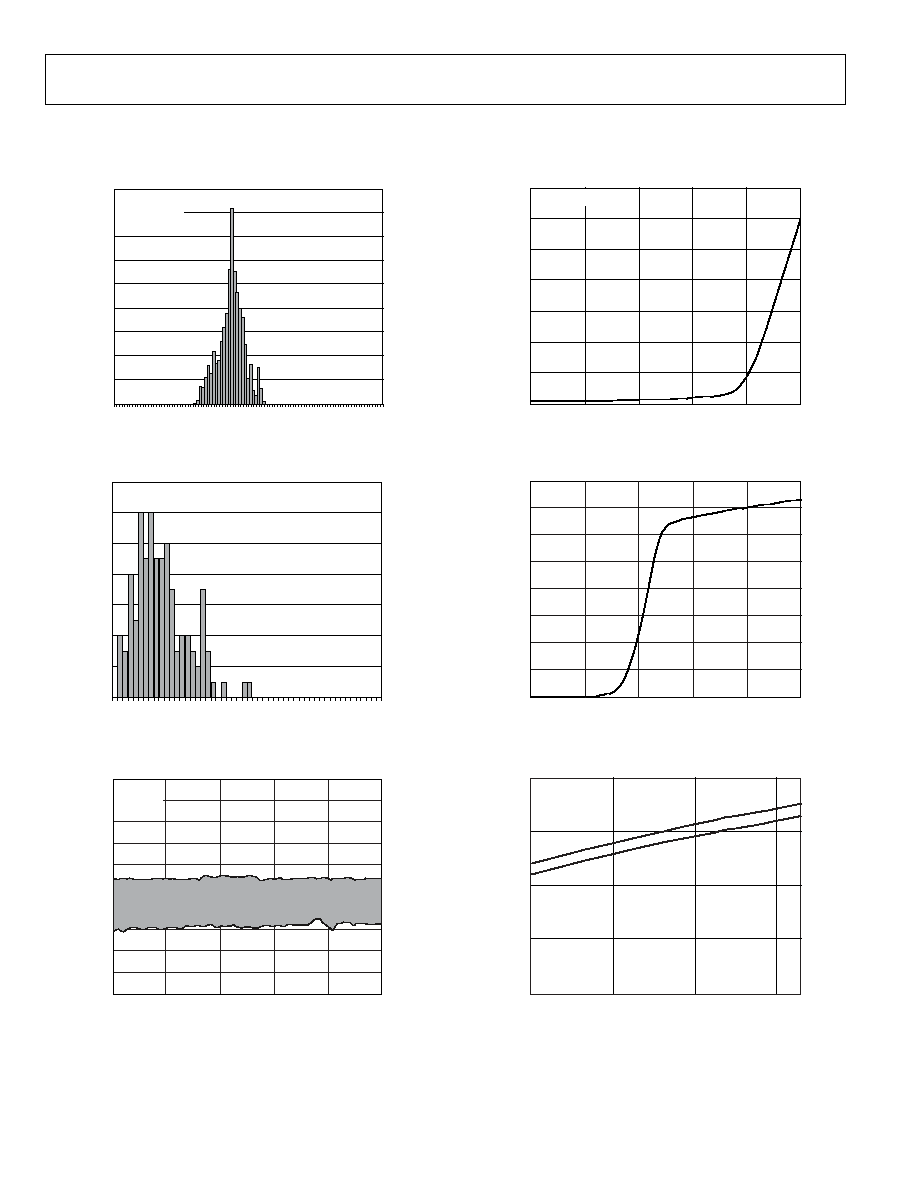
TYPICAL PERFORMANCE CHARACTERISTICS
V = 5 V or ±2.5 V, unless otherwise noted.
SY
700
0
100
200
300
400
500
600
25
45
65
85
105
125
05
62
4-
00
6
TEMPERATURE (°C)
I
NP
UT
B
I
A
S
CURR
E
NT
(
p
A)
V
SY
= 5V AND 2.7V
450
0
10.0
05
62
4-
00
3
INPUT OFFSET VOLTAGE (µV)
N
U
M
B
E
R
O
F
A
M
P
L
I
F
IE
R
S
50
100
150
200
250
300
350
400
V
SY
= 5V
0V < V
CM
< 5V
T
A
= 25°C
8.4 6.8 5.2 3.6 2.0 0.4 1.2 2.8 4.4 6.0 7.6 9.2
Figure 6. Input Bias Current vs. Temperature
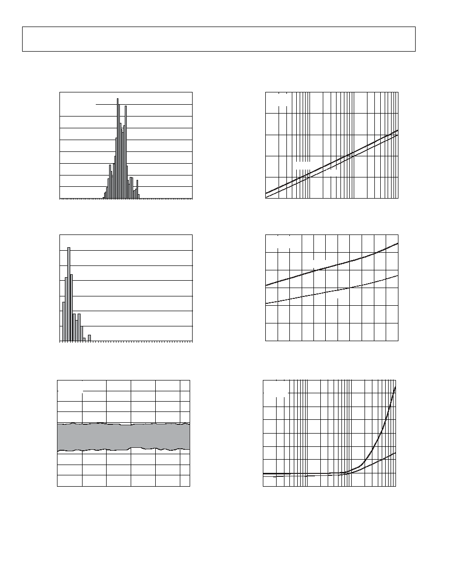
Figure 3. Input Offset Voltage Distribution
14
0
0
0.09
05
624
-
00
4
TCV
OS
(µV/°C)
N
U
M
B
E
R
OF
A
M
P
L
IF
IE
R
S
6
160
0
0
5
05
62
4-
00
7
SUPPLY VOLTAGE (V)
S
UP
P
L
Y
C
URRE
NT
(
µ
A)
2
4
6
8
10
12
0.012 0.024 0.036 0.048 0.060 0.072 0.084
V
SY
= 5V
40°C < T
A
< +125°C
20
40
60
80
100
120
140
1
2
3
4
T
A
= 25°C
Figure 7. Supply Current vs. Supply Voltage
Figure 4. Input Offset Voltage Drift Distribution
10
10
0
5
05
62
4-
00
5
INPUT COMMON-MODE VOLTAGE (V)
I
N
PU
T
O
F
F
SET
VO
L
T
A
G
E
(
µV
)
8
6
4
2
0
2
4
6
8
1
2
3
4
V
SY
= 5V
T
A
= 25°C
200
0
50
100
150
40
10
60
110
05
62
4-
00
8
TEMPERATURE (°C)
S
UP
P
L
Y
CURR
E
NT
(
µA
)
V
SY
= 5V
V
SY
= 2.7V
Figure 8. Supply Current vs. Temperature
Figure 5. Input Offset Voltage vs. Input Common-Mode Voltage
AD8538
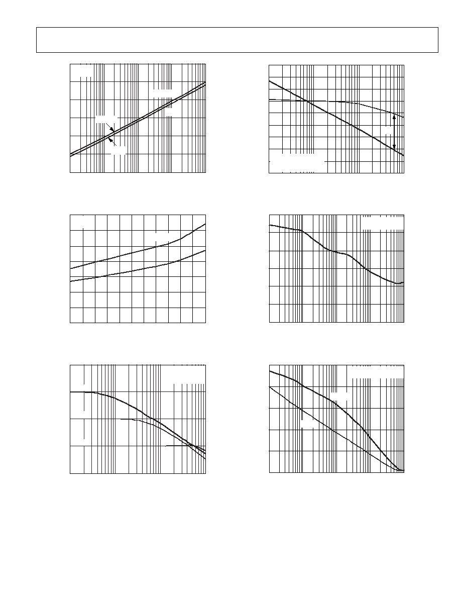
Rev. 0 | Page 7 of 12
10000
0.01
0.1
1
10
100
1000
0.001
10
1
0.1
0.01
05
62
4-
00
9
LOAD CURRENT (mA)
O
U
TP
U
T S
A
TU
R
A
T
I
O
N V
O
L
T
AG
E
(
m
V
)
V
SY
V
OH
V
SY
= 5V
T
A
= 25°C
SOURCE
SINK
V
OL
70
20
10
0
10
30
40
50
60
20
45
0
45
90
1k
10k
100k
1M
05
62
4-
0
12
FREQUENCY (Hz)
O
PEN
-LO
O
P
G
A
I
N
(dB
)
O
P
E
N
-
L
O
O
P P
HAS
E
S
H
I
F
T
(
D
eg
r
ees)
V
SY
= ±2.5V AND ±1.35V
R
L
= 100k
C
L
= 20pF
135
M
Figure 9. Output Saturation Voltage vs. Load Current
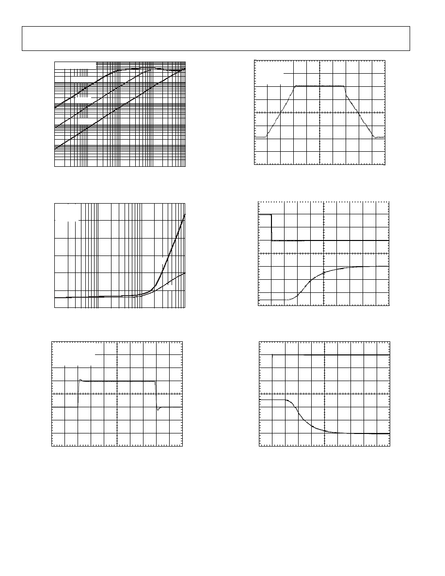
Figure 12. Open-Loop Gain and Phase vs. Frequency
35
0
5
10
15
20
25
30
40 25 10
5
20
35
50
65
80
95
110 125
05
62
4-
01
0
TEMPERATURE (°C)
O
U
TP
U
T S
A
TU
R
A
T
I
O
N V
O
L
T
AG
E
(
m
V
)
V
SY
V
OH
V
SY
= 5V
R
L
= 10k
V
OL
120
0
100
1M
05
62
4-
0
13
FREQUENCY (Hz)
CM
RR
(
d
B
)
20
40
60
80
100
1k
10k
100k
V
SY
= 5V AND 2.7V
T
A
= 25°C
Figure 13. CMRR vs. Frequency
Figure 10. Output Saturation Voltage vs. Temperature
60
20
1k
10k
100k
1M
05
62
4-
0
1
1
FREQUENCY (Hz)
C
L
OS
E
D
-
L
OOP
GA
IN
(
d
B
)
0
20
40
V
SY
= 5V AND 2.7V
C
L
= 20pF
R
L
= 2k
A
V
= 10
A
V
= 100
A
V
= 1
100
0
100
1M
05
62
4-
0
14
FREQUENCY (Hz)
P
S
RR (
d
B
)
20
40
60
80
1k
10k
100k
V
SY
= ±2.5V AND ±1.35V
T
A
= 25°C
+PSRR
PSRR
Figure 14. PSRR vs. Frequency
Figure 11. Closed-Loop Gain vs. Frequency
AD8538
Rev. 0 | Page 8 of 12
TIME (4µs/DIV)
V
O
L
T
A
G
E (
1
V/
D
I
V)
05
62
4-
01
7
V
SY
= 5V
A
V
= 1
C
L
= 300pF
R
L
= 10k
1000
0.01
1
0.1
10
100
100
1k
10k
100k
1M
05
62
4-
02
2
FREQUENCY (Hz)
O
UT
P
UT
I
M
P
E
DANCE
(
)
V
SY
= 5V AND 2.7V
A
V
= 1
A
V
= 10
A
V
= 100
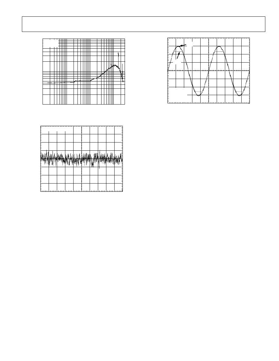
Figure 18. Large Signal Transient Response
Figure 15. Closed-Loop Output Impedance vs. Frequency
TIME (10µs/DIV)
05
62
4-
0
18
V
SY
= 5V
A
V
= 50
V
OU
T
(V
)
V
IN
(m
V)
100
0
0
2.5
60
0
1
1000
05
62
4-
01
5
LOAD CAPACITANCE (pF)
SM
A
L
L
SI
G
N
A
L
O
VER
S
H
O
O
T
(
%
)
10
20
30
40
50
10
100
V
SY
= 5V
T
A
= 25°C
R
L
= 2k
OS+
OS
Figure 16. Small Signal Overshoot vs. Load Capacitance
Figure 19. Positive Overload Recovery
TIME (4µs/DIV)
V
O
L
T
A
G
E (
5
0
m
V/
D
I
V)
05
62
4-
01
6
V
SY
= 5V AND 2.7V
A
V
= 1
C
L
= 300pF
R
L
= 2k
TIME (10µs/DIV)
V
OU
T
(V
)
V
IN
(m
V)
05
62
4-
01
9
V
SY
= 5V
A
V
= 50
0
100
2.5
0
Figure 17. Small Signal Transient Response
Figure 20. Negative Overload Recovery
AD8538
Rev. 0 | Page 9 of 12
TIME (200µs/DIV)
V
O
L
T
A
G
E (
1
V/
D
I
V)
05
62
4-
02
3
V
SY
= 5V
A
V
= 1
V
IN
= 6V p-p
R
L
= 10k
V
OUT
V
IN
1000
10
100
10
100
1k
10k
05
62
4-
02
1
FREQUENCY (Hz)
V
O
L
T
AG
E
NO
I
S
E
DE
NS
I
T
Y (
n
V
/
Hz
)
V
SY
= 5V
T
A
= 25°C
Figure 23. No Phase Reversal
Figure 21. Voltage Noise Density
TIME (1s/DIV)
V
O
L
T
AG
E
(
500n
V
/
DI
V
)
05
62
4-
0
20
V
SY
= 5V AND 2.7V
Figure 22. 0.1 Hz to 10 Hz Input Voltage Noise
AD8538
Rev. 0 | Page 10 of 12
V = 2.7 V or ±1.35 V.
S
180
0
05
62
4-
02
4
INPUT OFFSET VOLTAGE (µV)
N
U
M
B
E
R
OF
A
M
P
L
IF
IE
R
S
20
40
60
80
100
120
140
160
10.0 8.4 6.8 5.2 3.6 2.0 0.4 1.2 2.8 4.4 6.0 7.6 9.2
V
SY
= 2.7V
0V < V
CM
< 2.7V
T
A
= 25°C
10000
0.1
0.001
1
05
62
4-
02
7
LOAD CURRENT (mA)
O
U
T
P
U
T
SA
T
U
R
A
T
I
O
N
VO
L
T
A
G
E
(m
V)
1
10
100
1000
0.01
0.1
SINK
SOURCE
V
SY
= 2.7V
T
A
= 25°C
Figure 24. Input Offset Voltage Distribution
Figure 27. Output Saturation Voltage vs. Load Current
30
0
40
125
05
62
4-
02
8
TEMPERATURE (°C)
O
U
T
P
U
T
SA
T
U
R
A
T
I
O
N
VO
L
T
A
G
E
(m
V)
5
10
15
20
25
25 10
5
20
35
50
65
80
95
110
V
SY
= 2.7V
R
L
= 10k
V
SY
= VOH
VOL
35
0
05
624
-
02
5
TCV
OS
(µV/°C)
N
U
M
B
E
R
OF
A
M
P
L
IF
IE
R
S
5
10
15
20
25
30
0
0.012 0.024 0.036 0.048 0.060 0.072 0.084 0.096
V
SY
= 2.7V
40°C < T
A
< +125°C
Figure 25. Input Offset Voltage Drift Distribution
Figure 28. Output Saturation Voltage vs. Temperature
10
10
0
2
05
62
4-
02
6
INPUT COMMON-MODE VOLTAGE (V)
I
N
PU
T
O
F
F
SET
VO
L
T
A
G
E
.5
(
µV
)
8
6
4
2
0
2
4
6
8
0.5
1.0
1.5
2.0
V
SY
= 2.7V
T
A
= 25°C
80
0
1
1
05
62
4-
02
9
LOAD CAPACITANCE (pF)
S
M
A
L
L
S
IGN
A
L
OV
E
R
S
H
OOT
(
%
)
000
10
20
30
40
50
60
70
10
100
OS+
OS
V
SY
= 2.7V
T
A
= 25°C
R
L
= 2k
Figure 29. Small Signal Overshoot vs. Load Capacitance
Figure 26. Input Offset Voltage vs. Input Common-Mode Voltage
AD8538
Rev. 0 | Page 11 of 12
TIME (4µs/DIV)
V
O
L
T
A
G
E
(
500m
V
/
DI
V
)
05
62
4-
03
0
V
SY
= 2.7V
A
V
= 1
C
L
= 100pF
R
L
= 10k
1000
10
100
10
100
1k
10k
100k
05
62
4-
03
2
FREQUENCY (Hz)
V
O
L
T
AG
E
NO
I
S
E
DE
NS
I
T
Y (
n
V
/
Hz
)
V
SY
= 2.7V
T
A
= 25°C
Figure 30. Large Signal Transient Response
Figure 31. Voltage Noise Density
AD8538
Rev. 0 | Page 12 of 12
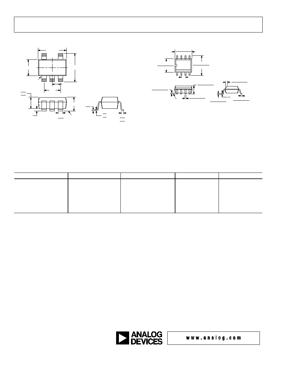
OUTLINE DIMENSIONS
*COMPLIANT TO JEDEC STANDARDS MO-193-AB WITH
THE EXCEPTION OF PACKAGE HEIGHT AND THICKNESS.
PIN 1
1.60 BSC
2.80 BSC
1.90
BSC
0.95 BSC
0.20
0.08
0.60
0.45
0.30
8°
4°
0°
0.50
0.30
0.10 MAX
SEATING
PLANE
*1.00 MAX
*0.90
0.87
0.84
2.90 BSC
5
4
1
2
3
0.25 (0.0098)
0.17 (0.0067)
1.27 (0.0500)
0.40 (0.0157)
0.50 (0.0196)
0.25 (0.0099)
× 45°
8°
0°
1.75 (0.0688)
1.35 (0.0532)
SEATING
PLANE
0.25 (0.0098)
0.10 (0.0040)
4
1
8
5
5.00 (0.1968)
4.80 (0.1890)
4.00 (0.1574)
3.80 (0.1497)
1.27 (0.0500)
BSC
6.20 (0.2440)
5.80 (0.2284)
0.51 (0.0201)
0.31 (0.0122)
COPLANARITY
0.10
CONTROLLING DIMENSIONS ARE IN MILLIMETERS; INCH DIMENSIONS
(IN PARENTHESES) ARE ROUNDED-OFF MILLIMETER EQUIVALENTS FOR
REFERENCE ONLY AND ARE NOT APPROPRIATE FOR USE IN DESIGN.
COMPLIANT TO JEDEC STANDARDS MS-012-AA
Figure 32. 5-Lead Thin Small Outline Transistor Package [TSOT_23]
(UJ-5)
Dimensions shown in millimeters
Figure 33. 8-Lead Standard Small Outline Package [SOIC_N]
Narrow Body
(R-8)
Dimensions shown in millimeters and (inches)
ORDERING GUIDE
Model
Temperature Range
Package Description
Package Option
Branding
AD8538AUJZ-R2
-40°C to +125°C
5-Lead TSOT-23
UJ-5
AOC
1
AD8538AUJZ-REEL
-40°C to +125°C
5-Lead TSOT-23
UJ-5
AOC
1
AD8538AUJZ-REEL7
-40°C to +125°C
5-Lead TSOT-23
UJ-5
AOC
1
AD8538ARZ
-40°C to +125°C
8-Lead SOIC_N
R-8
1
AD8538ARZ-REEL
-40°C to +125°C
8-Lead SOIC_N
R-8
1
AD8538ARZ-REEL7
-40°C to +125°C
8-Lead SOIC_N
R-8
1
T
1
Z = Pb-free part.
© 2005 Analog Devices, Inc. All rights reserved. Trademarks and
registered trademarks are the property of their respective owners.
D05624-0-10/05(0)
TTT
Document Outline
- þÿ
- þÿ
- þÿ
- þÿ
- þÿ
- þÿ
- þÿ
- þÿ
- þÿ
- þÿ