 | ÐлекÑÑоннÑй компоненÑ: AD8555 | СкаÑаÑÑ:  PDF PDF  ZIP ZIP |
Äîêóìåíòàöèÿ è îïèñàíèÿ www.docs.chipfind.ru
Zero-Drift, Digitally Programmable
Sensor Signal Amplifier
AD8555
Rev. 0
Information furnished by Analog Devices is believed to be accurate and reliable.
However, no responsibility is assumed by Analog Devices for its use, nor for any
infringements of patents or other rights of third parties that may result from its use.
Specifications subject to change without notice. No license is granted by implication
or otherwise under any patent or patent rights of Analog Devices. Trademarks and
registered trademarks are the property of their respective owners.
One Technology Way, P.O. Box 9106, Norwood, MA 02062-9106, U.S.A.
Tel: 781.329.4700
www.analog.com
Fax: 781.326.8703
© 2004 Analog Devices, Inc. All rights reserved.
FEATURES
Very low offset voltage: 10 µV maximum over temperature
Very low input offset voltage drift: 60 nV/°C maximum
High CMRR: 96 dB minimum
Digitally programmable gain and output offset voltage
Single-wire serial interface
Open and short wire fault detection
Low-pass filtering
Stable with any capacitive load
Externally programmable output clamp voltage for driving
low voltage ADCs
LFCSP-16 and SOIC-8 packages
2.7 V to 5.5 V operation
-40°C to +125°C operation
APPLICATIONS
Automotive sensors
Pressure and position sensors
Thermocouple amplifiers
Industrial weigh scales
Precision current sensing
Strain gages
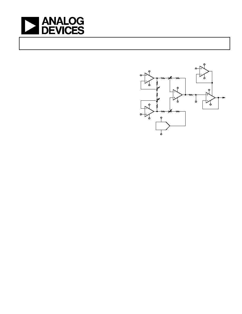
FUNCTIONAL BLOCK DIAGRAM
A3
A2
A4
A5
VDD
VDD
DAC
VSS
VSS
VDD
VSS
VDD
VDD
VSS
VCLAMP
VPOS
VSS
FILT/
DIGOUT
VOUT
A1
VDD
VSS
VNEG
R1
R3
R2
R5
R7
P4
R4
R6
RF
P3
P2
P1
04598-0-001
Figure 1.
GENERAL DESCRIPTION
The AD8555 is a zero-drift, sensor signal amplifier with digi-
tally programmable gain and output offset. Designed to easily
and accurately convert variable pressure sensor and strain
bridge outputs to a well-defined output voltage range, the
AD8555 also accurately amplifies many other differential or
single-ended sensor outputs. The AD8555 uses the ADI pat-
ented low noise auto-zero and DigiTrim® technologies to create
an incredibly accurate and flexible signal processing solution in
a very compact footprint.
Gain is digitally programmable in a wide range from 70 to 1,280
through a serial data interface. Gain adjustment can be fully
simulated in-circuit and then permanently programmed with
proven and reliable poly-fuse technology. Output offset voltage
is also digitally programmable and is ratiometric to the supply
voltage.
In addition to extremely low input offset voltage and input off-
set voltage drift and very high dc and ac CMRR, the AD8555
also includes a pull-up current source at the input pins and a
pull-down current source at the VCLAMP pin. This allows open
wire and shorted wire fault detection. A low-pass filter function
is implemented via a single low cost external capacitor. Output
clamping set via an external reference voltage allows the
AD8555 to drive lower voltage ADCs safely and accurately.
When used in conjunction with an ADC referenced to the same
supply, the system accuracy becomes immune to normal supply
voltage variations. Output offset voltage can be adjusted with a
resolution of better than 0.4% of the difference between VDD
and VSS. A lockout trim after gain and offset adjustment further
ensures field reliability.
The AD8555AR is fully specified over the extended industrial
temperature range of -40°C to +125°C. Operating from
single-supply voltages of 2.7 V to 5.5 V, the AD8555 is offered in
the narrow 8-lead SOIC package and the 4 mm × 4 mm
16-lead LFCSP.

AD8555
Rev. 0 | Page 2 of 28
TABLE OF CONTENTS
Electrical Specifications ................................................................... 3
Absolute Maximum Ratings............................................................ 7
Pin Configurations and Function Descriptions ........................... 8
Typical Performance Characteristics ............................................. 9
Theory of Operation ...................................................................... 17
Gain Values.................................................................................. 18
Open Wire Fault Detection ....................................................... 19
Shorted Wire Fault Detection ................................................... 19
Floating VPOS, VNEG, or VCLAMP Fault Detection........... 19
Device Programming................................................................. 19
Filtering Function....................................................................... 25
Driving Capacitive Loads.......................................................... 25
RF Interference ........................................................................... 26
Single-Supply Data Acquisition System .................................. 26
Using the AD8555 with Capacitive Sensors ........................... 27
Outline Dimensions ....................................................................... 28
Ordering Guide .......................................................................... 28
REVISION HISTORY
4/04--Revision 0: Initial Version

AD8555
Rev. 0 | Page 3 of 28
ELECTRICAL SPECIFICATIONS
At V
DD
= 5.0 V, V
SS
= 0.0 V, V
CM
= 2.5 V, V
O
= 2.5 V, -40°C T
A
+125°C, unless otherwise specified.
Table 1.
Parameter
Symbol
Conditions
Min
Typ
Max
Unit
INPUT STAGE
Input Offset Voltage
V
OS
2
10
µV
Input Offset Voltage Drift
T
C
V
OS
25 65
nV/°C
Input Bias Current
I
B
T
A
= 25°C
12
16
22
nA
25
nA
Input Offset Current
I
OS
T
A
= 25°C
0.2
1
nA
1.5
nA
Input Voltage Range
0.6
3.8
V
Common-Mode Rejection Ratio
CMRR
V
CM
= 0.9 V to 3.6 V, A
V
= 70
80
92
dB
V
CM
= 0.9 V to 3.6 V, A
V
= 1,280
96
112
dB
Linearity
V
O
= 0.2 V to 3.4 V
20
ppm
V
O
= 0.2 V to 4.8 V
1000
ppm
Differential Gain Accuracy
Second Stage Gain = 17.5 to 100
0.35
1.6
%
Second Stage Gain = 140 to 200
0.5
2.5
%
Differential Gain Temperature Coefficient
Second Stage Gain = 17.5 to 100
15
40
ppm/°C
Second Stage Gain = 140 to 200
40
100
ppm/°C
RF
14
18
22
k
RF Temperature Coefficient
700
ppm/°C
DAC
Accuracy
A
V
= 70, Offset Codes = 8 to 248
0.7
0.8
%
Ratiometricity
A
V
= 70, Offset Codes = 8 to 248
50
ppm
Output Offset
A
V
= 70, Offset Codes = 8 to 248
5
35
mV
Temperature Coefficient
3.3
15
ppm FS/°C
VCLAMP
Input Bias Current
T
A
= 25°C, VCLAMP = 5 V
200
nA
500
nA
Input Voltage Range
1.25
4.94
V
OUTPUT BUFFER STAGE
Buffer Offset
7
15
mV
Short-Circuit Current
I
SC
5
10
mA
Output Voltage, Low
V
OL
R
L
= 10 k to 5 V
30
mV
Output Voltage, High
V
OH
R
L
= 10 k to 0 V
4.94
V
POWER SUPPLY
Supply Current
I
SY
V
O
= 2.5 V, VPOS = VNEG = 2.5V,
VDAC Code = 128
2.0
2.5
mA
Power Supply Rejection Ratio
PSRR
A
V
= 70
109
125
dB
DYNAMIC PERFORMANCE
Gain Bandwidth Product
GBP
First Gain Stage, T
A
= 25°C
2
MHz
Second Gain Stage, T
A
= 25°C
8
MHz
Output Buffer Stage
1.5
MHz
Output Buffer Slew Rate
SR
A
V
= 70, R
L
= 10 k, C
L
= 100 pF
1.2
V/µs
Settling Time
t
s
To 0.1%, A
V
= 70, 4 V Output Step
8
µs
NOISE PERFORMANCE
Input Referred Noise
T
A
= 25°C, f = 1 kHz
32
nV/Hz
Low Frequency Noise
e
n p-p
f = 0.1 Hz to 10 Hz
0.5
µV p-p
Total Harmonic Distortion
THD
V
IN
= 16.75 mV rms, f = 1 kHz, A
V
= 100
-100
dB

AD8555
Rev. 0 | Page 4 of 28
Parameter
Symbol
Conditions
Min
Typ
Max
Unit
DIGITAL INTERFACE
Input Current
2
µA
DIGIN Pulse Width to Load 0
t
w0
T
A
= 25°C
0.05
10
µs
DIGIN Pulse Width to Load 1
t
w1
T
A
= 25°C
50
µs
Time between Pulses at DIGIN
t
ws
T
A
= 25°C
10
µs
DIGIN Low
T
A
= 25°C
1
V
DIGIN High
T
A
= 25°C
4
V
DIGOUT Logic 0
T
A
= 25°C
1
V
DIGOUT Logic 1
T
A
= 25°C
4
V

AD8555
Rev. 0 | Page 5 of 28
At V
DD
= 2.7 V, V
SS
= 0.0 V, V
CM
= 1.35 V, V
O
= 1.35 V, -40°C T
A
+125°C, unless otherwise specified.
Table 2.
Parameter
Symbol
Conditions
Min
Typ
Max
Unit
INPUT STAGE
Input Offset Voltage
V
OS
2
10
µV
Input Offset Voltage Drift
T
C
V
OS
25 60
nV/°C
Input Bias Current
I
B
T
A
= 25°C
12
16
nA
Input Offset Current
I
OS
T
A
= 25°C
0.2
1
nA
1.5
nA
Input Voltage Range
0.5
1.6
V
Common-Mode Rejection Ratio
CMRR
V
CM
= 0.9 V to 1.3 V, A
V
= 70
80
92
dB
V
CM
= 0.9 V to 1.3 V, A
V
= 1,280
96
112
dB
Linearity
V
O
= 0.2 V to 3.4 V
20
ppm
V
O
= 0.2 V to 4.8 V
1000
ppm
Differential Gain Accuracy
Second Stage Gain = 17.5 to 100
0.35
%
Second Stage Gain = 140 to 200
0.5
%
Differential Gain Temperature Coefficient
Second Stage Gain = 17.5 to 100
15
ppm/°C
Second Stage Gain = 140 to 200
40
ppm/°C
RF
14
18
22
k
RF Temperature Coefficient
700
ppm/°C
DAC
Accuracy
A
V
= 70, Offset Codes = 8 to 248
0.7
%
Ratiometricity
A
V
= 70, Offset Codes = 8 to 248
50
ppm
Output Offset
A
V
= 70, Offset Codes = 8 to 248
5
35
mV
Temperature Coefficient
3.3
ppm FS/°C
VCLAMP
Input Bias Current
T
A
= 25°C, VCLAMP = 2.7 V
200
nA
500
nA
Input Voltage Range
1.25
2.64
V
OUTPUT BUFFER STAGE
Buffer Offset
7
15
mV
Short-Circuit Current
I
SC
4.5
9.5
mA
Output Voltage, Low
V
OL
R
L
= 10 k to 5 V
30
mV
Output Voltage, High
V
OH
R
L
= 10 k to 0 V
2.64
V
POWER SUPPLY
Supply Current
I
SY
V
O
= 1.35 V, VPOS = VNEG = 1.35 V,
VDAC Code = 128
2.0
mA
Power Supply Rejection Ratio
PSRR
A
V
= 70
109
125
dB
DYNAMIC PERFORMANCE
Gain Bandwidth Product
GBP
First Gain Stage, T
A
= 25°C
2
MHz
Second Gain Stage, T
A
= 25°C
8
MHz
Output Buffer Stage
1.5
MHz
Output Buffer Slew Rate
SR
A
V
= 70, R
L
= 10 k, C
L
= 100 pF
1.2
V/µs
Settling Time
t
s
To 0.1%, A
V
= 70, 4 V Output Step
8
µs
NOISE PERFORMANCE
Input Referred Noise
T
A
= 25°C, f = 1 kHz
32
nV/Hz
Low Frequency Noise
e
n
p-p
f = 0.1 Hz to 10 Hz
0.3
µV p-p
Total Harmonic Distortion
THD
V
IN
= 16.75 mV rms, f = 1 kHz, A
V
= 100
-100
dB

AD8555
Rev. 0 | Page 6 of 28
Parameter
Symbol
Conditions
Min
Typ
Max
Unit
DIGITAL INTERFACE
Input Current
2
µA
DIGIN Pulse Width to Load 0
t
w0
T
A
= 25°C
0.05
10
µs
DIGIN Pulse Width to Load 1
t
w1
T
A
= 25°C
50
µs
Time between Pulses at DIGIN
t
ws
T
A
= 25°C
10
µs
AD8555
Rev. 0 | Page 7 of 28
ABSOLUTE MAXIMUM RATINGS
Table 3.
Parameter Rating
Supply Voltage
6 V
Input Voltage
VSS - 0.3 V to VDD + 0.3 V
Differential Input Voltage
1
±5.0
V
Output Short-Circuit
Duration to VSS or VDD
Indefinite
Storage Temperature Range
-65°C to +150°C
Operating Temperature Range
-40°C to +125°C
Junction Temperature Range
-65°C to +150°C
Lead Temperature Range
(Soldering, 10 sec)
300°C
Table 4.
Package Type
JA
2
JC
Unit
8-Lead SOIC (R)
158
43
°C/W
16-Lead LFCSP (CP)
44
31.5
°C/W
1
Differential input voltage is limited to ±5.0 V or ± the supply voltage, which-
ever is less.
2
JA
is specified for the worst-case conditions, i.e.,
JA
is specified for device
soldered in circuit board for SOIC and LFCSP packages.
AD8555
Rev. 0 | Page 8 of 28
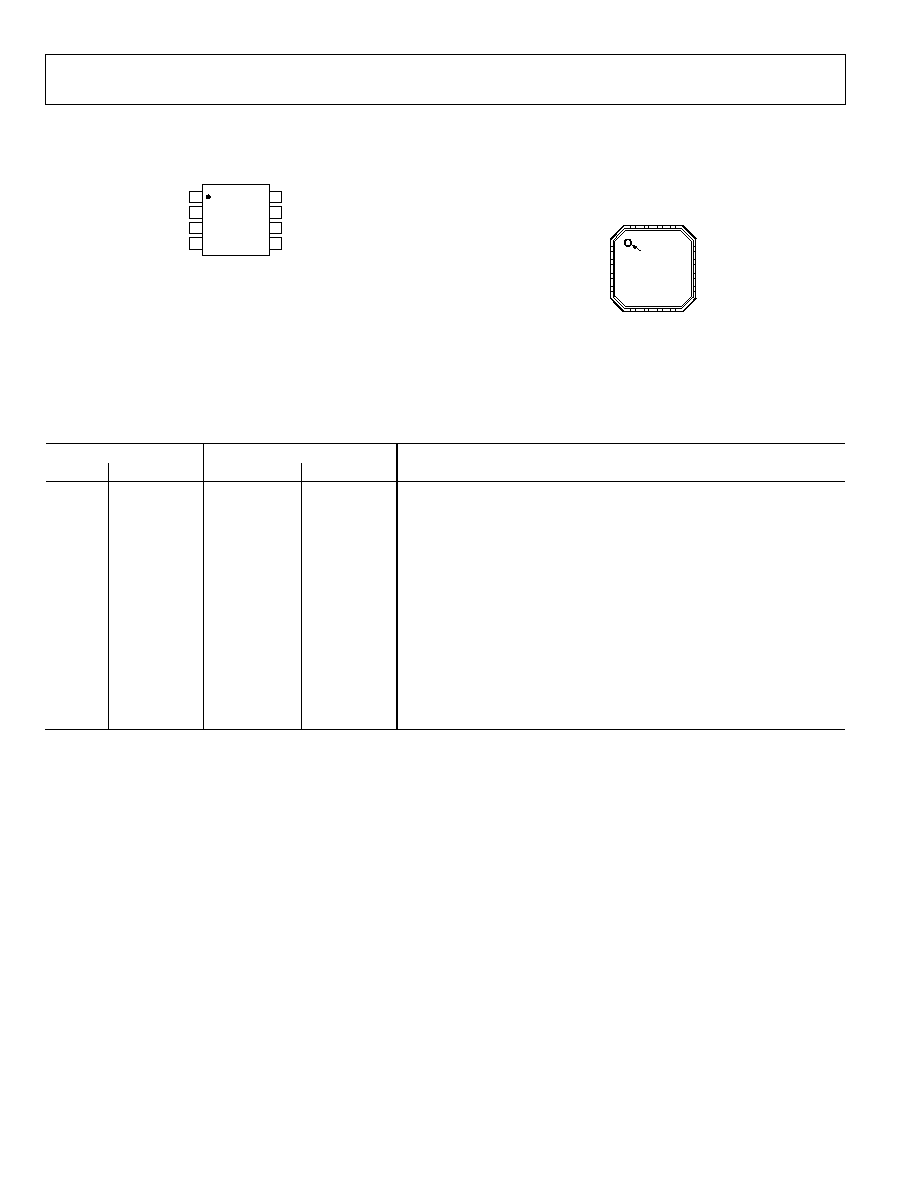
PIN CONFIGURATIONS AND FUNCTION DESCRIPTIONS
VSS
8
VOUT
7
VCLAMP
6
VPOS
5
VDD
1
FILT/DIGOUT
2
DIGIN
3
VNEG
4
AD8555
TOP VIEW
(Not to Scale)
04598-0-049
Figure 2. 8-Lead SOIC (Not Drawn to Scale)
04598-0-050
12
11
10
9
NC
VCLAMP
NC
VOUT
1
NC
2
3
5
NC
VN
EG
NC
VPOS
6
7
8
4
DIGIN
NC
FILT/DIGOUT
16
15
14
13
AD8555
TOP VIEW
PIN 1
INDICATOR
AV
DD
DV
DD
A
VSS
D
VSS
NC = NO CONNECT
Figure 3. 16-Lead LFCSP (Not Drawn to Scale)
Table 5. Pin Configuration
SOIC LFCSP
Pin No.
Mnemonic
Pin No.
Mnemonic
Description
1 VDD
N/A
N/A
Positive
Supply
Voltage.
2
FILT/DIGOUT
2
FILTDIGOUT
Unbuffered Amplifier Output In Series with a Resistor RF. Adding a capacitor
between FILT and VDD or VSS implements a low-pass filtering function. In
read mode, this pin functions as a digital output.
3
DIGIN
4
DIGIN
Digital Input.
4
VNEG
6
VNEG
Negative Amplifier Input (Inverting Input).
5
VPOS
8
VPOS
Positive Amplifier Input (Noninverting Input).
6
VCLAMP
10
VCLAMP
Set Clamp Voltage at Output.
7
VOUT
12
VOUT
Buffered Amplifier Output. Buffered version of the signal at the FILT/DIGOUT
pin. In read mode, VOUT is a buffered digital output.
8
VSS
N/A
N/A
Negative Supply Voltage.
N/A
N/A
13, 14
DVSS, AVSS
Negative Supply Voltage.
N/A
N/A
15, 16
DVDD, AVDD
Positive Supply Voltage.
N/A
N/A
1, 3, 5, 7, 9, 11
NC
Do Not Connect.
AD8555
Rev. 0 | Page 9 of 28
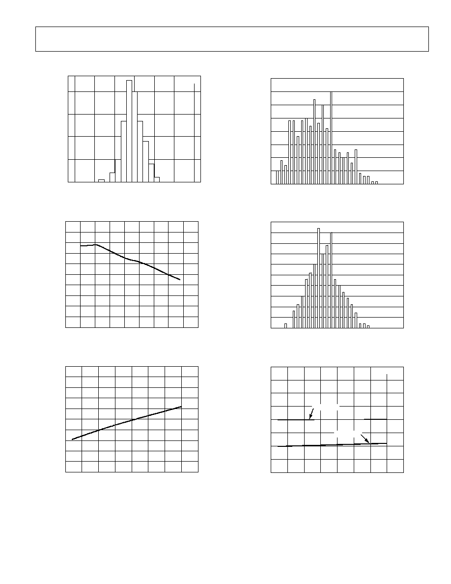
TYPICAL PERFORMANCE CHARACTERISTICS
04598-0-005
V
OS
(
µ
V)
9
9
6
3
3
6
0
NUMBE
R OF AMP
LIFIE
RS
0
30
20
40
10
V
S
= 5V
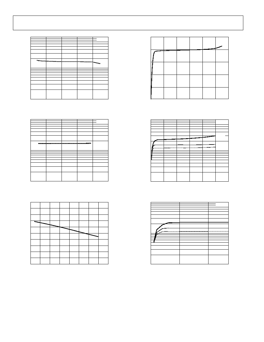
Figure 4. Input Offset Voltage Distribution
04598-0-061
V
CM
(V)
4.5
0
0.5
1.0
1.5
2.0
2.5
3.0
3.5
4.0
V
OS
(
µ
V)
1.0
0.5
0
0.5
1.0
1.5
2.0
2.5
3.0
3.5
4.0
Figure 5. Input Offset Voltage vs. Common-Mode Voltage
04598-0-062
TEMPERATURE (°C)
150
50
25
0
25
50
75
100
125
IN
PU
T OFFSET VOLTA
GE (
µ
V)
10
8
6
4
2
0
2
4
6
8
10
Figure 6. Input Offset Voltage vs. Temperature
04598-0-006
T
C
V
OS
(nV/°C)
75.0
50.0
62.5
37.5
25.0
12.5
0
NUMBE
R OF AMP
LIFIE
RS
0
40
30
35
25
20
15
10
5
V
S
= 5V
Figure 7. T
C
V
OS
@ V
S
= 5 V
04598-0-007
T
C
V
OS
(nV/°C)
0
12.5
25.0
37.5
50.0
62.5
75.0
NUMBE
R OF AMP
LIFIE
RS
0
50
40
35
25
45
15
5
30
20
10
Figure 8. T
C
V
OS
@ V
S
= 2.7 V
04598-0-008
TEMPERATURE (°C)
150
50
25
0
25
50
75
100
125
BUF V
OS
(mV
)
10.0
10.0
7.5
5.0
2.5
0
2.5
5.0
7.5
VOUT = 0.3V
VOUT = 4.7V
V
S
= 5V
Figure 9. Output Buffer Offset vs. Temperature
AD8555
Rev. 0 | Page 10 of 28
04598-0-009
TEMPERATURE (°C)
175
75
25
25
75
125
I
B
(nA)
1
100
10
V
S
= 5V
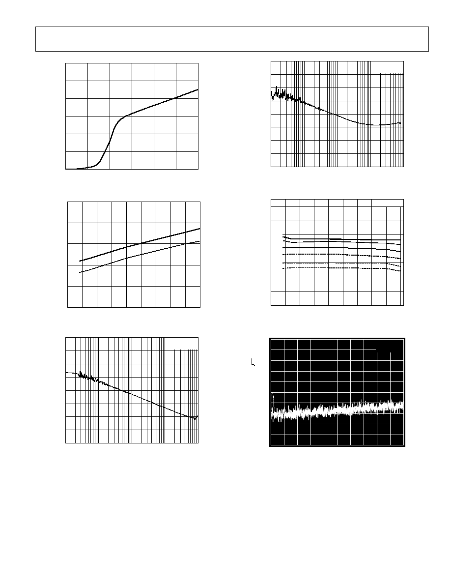
Figure 10. Input Bias Current at VPOS, VNEG vs. Temperature
04598-0-010
V
CM
(V)
5
0
1
2
3
4
I
B
(nA)
1
100
10
V
S
= 5V
Figure 11. Input Bias Current at VPOS, VNEG vs. Common-Mode Voltage
04598-0-063
TEMPERATURE (°C)
150
50
25
0
25
50
75
100
125
I
OS
(nA)
0.5
0.4
0.2
0.1
0
0.3
0.1
0.2
0.3
0.4
0.5
Figure 12. Input Offset Current vs. Temperature
04598-0-011
DIGITAL INPUT VOLTAGE (V)
6
0
1
2
3
4
5
DIGITAL INP
U
T CURRE
NT (
µ
A)
0
2.5
2.0
1.5
1.0
0.5
V
S
= 5.5V
Figure 13. Digital Input Current vs. Digital Input Voltage (Pin 3)
04598-0-012
VCLAMP VOLTAGE (V)
6
0
2
3
1
4
5
CLAMP
CURRE
NT (nA)
10
1000
100
40°C
+25°C
+125°C
V
S
= 5V
Figure 14. VCLAMP Current Over Temperature at V
S
= 5 V vs. VCLAMP Voltage
04598-0-013
VCLAMP VOLTAGE (V)
2.7
0
2
1
CLAMP
CURRE
NT (nA)
10
1000
100
40
+25
+125
V
S
= 2.7V
Figure 15. VCLAMP Current Over Temperature at V
S
= 2.7 vs. VCLAMP Voltage
AD8555
Rev. 0 | Page 11 of 28
04598-0-014
SUPPLY VOLTAGE (V)
6
0
2
3
1
4
5
S
U
P
P
L
Y
CURRE
NT (mA)
0
3
2
1
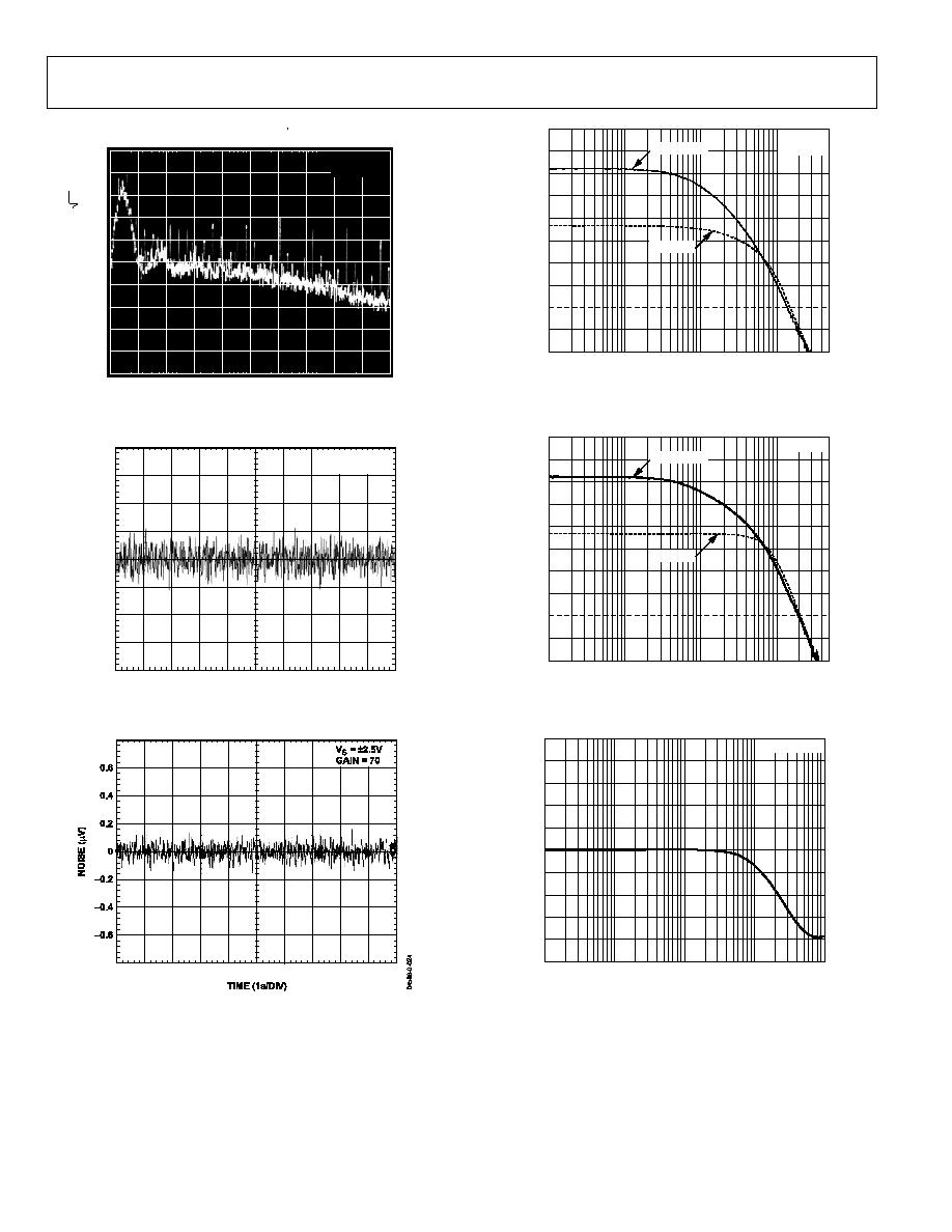
Figure 16. Supply Current (I
SY
) vs. Supply Voltage
04598-0-015
TEMPERATURE (°C)
150
75
50
25
0
25
50
75
100
125
5V
2.7V
S
U
P
P
L
Y
CURRE
NT (mA)
0.5
3.0
2.5
2.0
1.5
1.0
Figure 17. Supply Current (I
SY
) vs. Temperature
04598-0-016
FREQUENCY (Hz)
1M
100k
100
1k
10k
CMRR (dB)
40
80
120
0
V
S
= ±2.5V
GAIN = 70
Figure 18. CMRR vs. Frequency
04598-0-017
FREQUENCY (Hz)
1M
100
1k
10k
100k
CMRR (dB)
120
80
40
0
V
S
= ±2.5V
GAIN = 1280
Figure 19. CMRR vs. Frequency
04598-0-018
TEMPERATURE (°C)
75
50
0
25
75
50
25
100
125
150
CMRR (dB)
75
145
125
135
95
105
115
85
V
S
= 5V
70
100
200
400
800
1280
Figure 20. CMRR vs. Temperature at Different Gains
04598-0-019
FREQUENCY (kHz)
10
5
0
VOLTA
GE N
OISE D
E
N
S
ITY (
n
V/ H
z
)
60
50
40
30
20
10
V
S
= ±2.5V
GAIN = 70
Figure 21. Input Voltage Noise Density vs. Frequency (0 Hz to 10 kHz)
AD8555
Rev. 0 | Page 12 of 28
04598-0-021
FREQUENCY (kHz)
500
250
0
VOLTA
GE N
OISE D
E
N
S
ITY (
n
V/ H
z
)
30
25
20
15
10
5
V
S
= ±2.5V
GAIN = 70
35
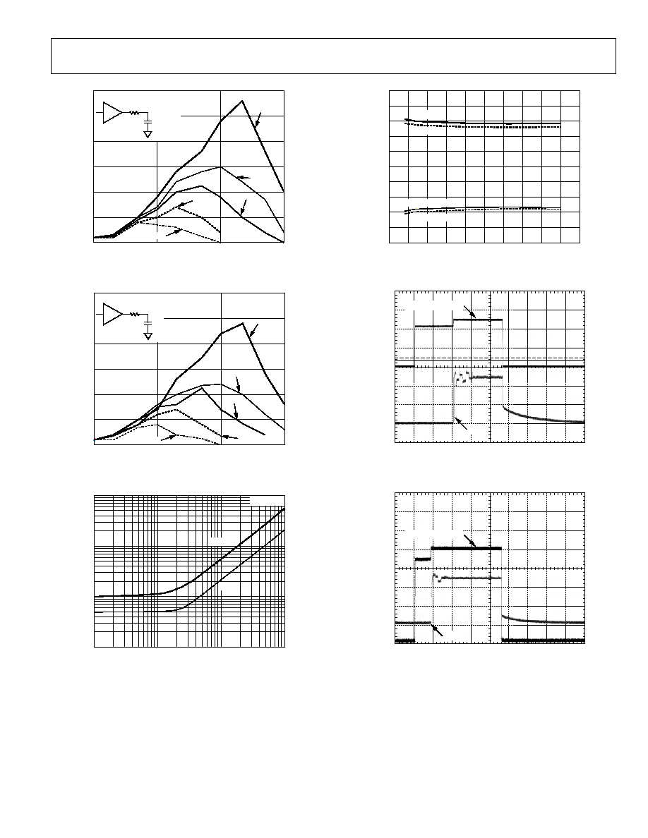
Figure 22. Input Voltage Noise Density vs. Frequency (0 Hz to 500 kHz)
04598-0-023
TIME (1s/DIV)
N
OISE (
µ
V)
0.6
0.4
0.2
0
0.2
0.4
0.6
V
S
= ±2.5V
GAIN = 1000
Figure 23. Low Frequency Input Voltage Noise (0.1 Hz to 10 Hz)
Figure 24. Low Frequency Input Voltage Noise (0.1 Hz to 10 Hz)
04598-0-025
FREQUENCY (Hz)
1k
100k
10k
1M
GAIN = 1280
GAIN = 70
V
S
= ±2.5V
C
L
= 40PF
CLOSED-
L
OOP GAIN (
d
B)
60
40
20
0
Figure 25. Closed-Loop Gain vs. Frequency Measured at Filter Pin
04598-0-026
FREQUENCY (Hz)
1k
100k
10k
1M
GAIN = 70
GAIN = 1280
V
S
= ±2.5V
CLOSED-
L
OOP GAIN (
d
B)
60
40
20
0
Figure 26. Closed-Loop Gain vs. Frequency Measured at Output Pin
04598-0-027
FREQUENCY (Hz)
1k
100k
10k
1M
10M
V
S
= ±2.5V
GAIN (
d
B)
4
8
0
4
8
Figure 27. Output Buffer Gain vs. Frequency
AD8555
Rev. 0 | Page 13 of 28
04598-0-028
LOAD CAPACITANCE (nF)
100.0
0.1
1.0
10.0
OVER
SH
OOT (
%
)
60
50
40
30
20
10
0
R
S
C
L
= 1nF
OUTPUT
BUFFER
V
S
= ±2.5V
R
S
= 0
R
S
= 10
R
S
= 20
R
S
= 50
R
S
= 100
Figure 28. Output Buffer Positive Overshoot
04598-0-029
LOAD CAPACITANCE (nF)
100.0
0.1
1.0
10.0
OVER
SH
OOT (
%
)
60
50
40
30
20
10
0
R
S
C
L
V
S
= ±2.5V
R
S
= 0
R
S
= 10
R
S
= 20
R
S
= 50
R
S
= 100
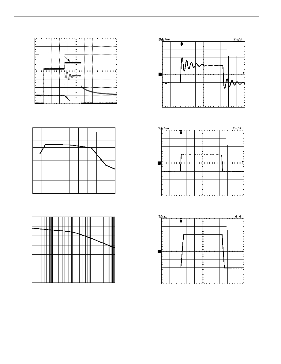
Figure 29. Output Buffer Negative Overshoot
04598-0-030
LOAD CURRENT (mA)
10.0
0.01
0.10
1.00
VDD
OUTPUT VOLTAGE (V)
0.001
1.000
0.100
0.010
V
S
= ±2.5V
SINK
SOURCE
Figure 30. Output Voltage to Supply Rail vs. Load Current
04598-0-031
TEMPERATURE (°C)
175
75
50
25
0
25
50
75
100
125
150
OUTP
UT S
H
ORT CIRCUIT (mA)
15
15
12
6
3
0
9
3
6
9
12
SOURCE 2.7V
SINK 5V
SOURCE 5V
SINK 2.7V
Figure 31. Output Short Circuit vs. Temperature
TIME (100
µ
s/DIV)
VOLTAGE
2
4
0
3
2
1
0
04598-0-032
SUPPLY VOLTAGE
V
OUT
Figure 32. Power-On Response at 25°C
TIME (100
µ
s/DIV)
VOLTA
GE (
1
V/D
IV)
5
6
4
3
2
1
0
04598-0-033
SUPPLY VOLTAGE
V
OUT
Figure 33. Power-On Response at 125°C
AD8555
Rev. 0 | Page 14 of 28
TIME (100
µ
s/DIV)
VOLTA
GE (
1
V/D
IV)
5
6
4
3
2
1
0
04598-0-034
SUPPLY VOLTAGE
V
OUT
Figure 34. Power-On Response at -40°C
04598-0-035
TEMPERATURE (°C)
150
75
50
25
0
25
50
75
100
125
P
S
RR (dB)
100
150
135
130
125
145
140
120
115
110
105
V
S
= 2.7V TO 5.5V
Figure 35. PSRR vs. Temperature
04598-0-068
FREQUENCY (kHz)
100
0.01
0.1
1
10
P
S
RR (dB)
140
120
100
80
60
40
20
0
Figure 36. PSRR vs. Frequency
04598-0-036
TIME (100
µ
s/DIV)
VOU
T
(
50mV/D
I
V)
2
T
V
S
= ±2.5V
GAIN = 70
C
L
= 0.1
µ
F
F
IN
= 10kHz
Figure 37. Small Signal Response
04598-0-037
TIME (100
µ
s/DIV)
VOU
T
(
50mV/D
I
V)
T
2
V
S
= ±2.5V
GAIN = 70
C
L
= 100pF
F
IN
= 1kHz
Figure 38. Small Signal Response
04598-0-038
TIME (10
µ
s/DIV)
VOU
T
(
1
V/D
I
V)
2
T
V
S
= ±2.5V
GAIN = 70
C
L
= 100pF
Figure 39. Large Signal Response
AD8555
Rev. 0 | Page 15 of 28
04598-0-039
TIME (10
µ
s/DIV)
VOU
T
(
1
V/D
I
V)
2
T
V
S
= ±2.5V
GAIN = 70
C
L
= 0.05
µ
F
Figure 40. Large Signal Response
04598-0-046
FREQUENCY (kHz)
0.1
10
1
100
1M
IMP
E
DANCE
(
)
1
10
100
1k
V
SY
= ±2.5V
A
V
= 70
Figure 41. Output Impedance vs. Frequency
04598-0-069
0V
0V
V
IN
V
OUT
Figure 42. Negative Overload Recovery (Gain = 70)
04598-0-070
V
IN
0V
0V
V
OUT
Figure 43. Positive Overload Recovery (Gain = 70)
04598-0-071
0V
0V
V
IN
2.5V
Figure 44. Negative Overload Recovery (Gain = 1280)
04598-0-072
V
IN
V
OUT
0V
0V
Figure 45. Positive Overload Recovery (Gain = 1280)
AD8555
Rev. 0 | Page 16 of 28
04598-0-073
0.1
µ
F
0.1
µ
F
V
294
20.5
+V
4
1
6
7
8
5
10k
1k
10k
OUT
AD8555
4V pp
GAIN = 70
OFFSET = 128
V
S
= ±2.5V
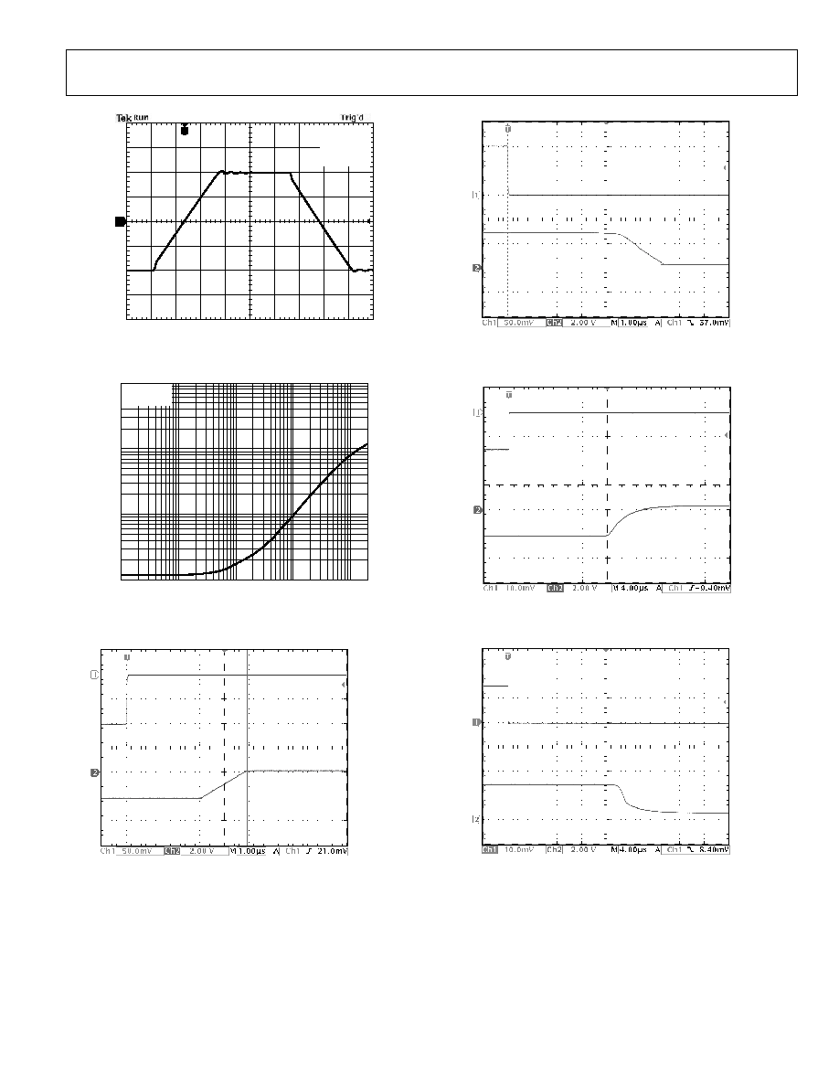
Figure 46. Settling Time 0.1%
04598-0-074
0.1
µ
F
0.1
µ
F
V
294
20.5
+V
4
1
6
7
8
5
10k
1k
10k
OUT
AD8555
4V pp
GAIN = 70
OFFSET = 128
V
S
= ±2.5V
Figure 47. Settling Time 0.01%
04598-0-075
FREQUENCY (Hz)
THD (%)
20
1k
2k
200
100
50
500
5k
10k
20k
0.10
1.00
0.20
0.50
0.02
0.05
0.01
V
S
= ±2.5V
Figure 48. THD vs. Frequency
AD8555
Rev. 0 | Page 17 of 28
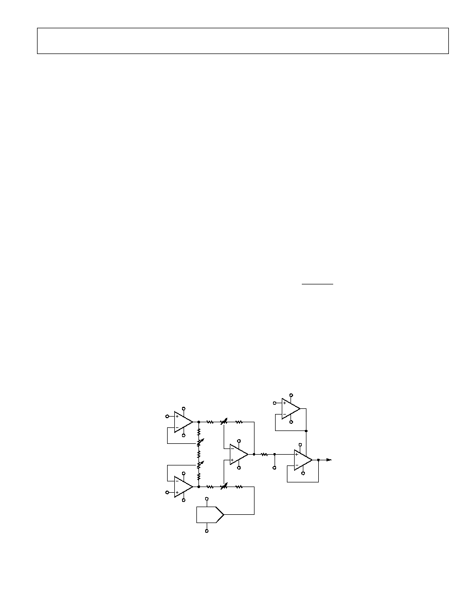
THEORY OF OPERATION
A1, A2, R1, R2, R3, P1, and P2 form the first gain stage of the
differential amplifier. A1 and A2 are auto-zeroed op amps that
minimize input offset errors. P1 and P2 are digital potentiome-
ters, guaranteed to be monotonic. Programming P1 and P2
allows the first stage gain to be varied from 4.0 to 6.4 with 7-bit
resolution (see Table 6 and Equation 3), giving a fine gain
adjustment resolution of 0.37%. R1, R2, R3, P1, and P2 each
have a similar temperature coefficient, so the first stage gain
temperature coefficient is lower than 100 ppm/°C.
A3, R4, R5, R6, R7, P3, and P4 form the second gain stage of the
differential amplifier. A3 is also an auto-zeroed op amp that
minimize input offset errors. P3 and P4 are digital potentiome-
ters, allowing the second stage gain to be varied from 17.5 to
200 in eight steps (see Table 7); they allow the gain to be varied
over a wide range. R4, R5, R6, R7, P3, and P4 each have a similar
temperature coefficient, so the second stage gain temperature
coefficient is lower than 100 ppm/°C.
RF together with an external capacitor connected between
FILT/DIGOUT and VSS or VDD form a low-pass filter. The
filtered signal is buffered by A4 to give a low impedance output
at VOUT. RF is nominally 16 k, allowing a 1 kHz low-pass
filter to be implemented by connecting a 10 nF external
capacitor between FILT/DIGOUT and VSS or between
FILT/DIGOUT and VDD. If low-pass filtering is not needed,
then the FILT/DIGOUT pin must be left floating.
A5 implements a voltage buffer, which provides the positive
supply to the amplifier output buffer A4. Its function is to limit
VOUT to a maximum value, useful for driving analog-to-digital
converters (ADC) operating on supply voltages lower than
VDD. The input to A5, VCLAMP, has a very high input resis-
tance. It should be connected to a known voltage and not left
floating. However, the high input impedance allows the clamp
voltage to be set using a high impedance source, e.g., a potential
divider. If the maximum value of VOUT does not need to be
limited, VCLAMP should be connected to VDD.
A4 implements a rail-to-rail input and output unity-gain volt-
age buffer. The output stage of A4 is supplied from a buffered
version of VCLAMP instead of VDD, allowing the positive
swing to be limited. The maximum output current is limited
between 5 mA to 10 mA.
An 8-bit digital-to-analog converter (DAC) is used to generate a
variable offset for the amplifier output. This DAC is guaranteed
to be monotonic. To preserve the ratiometric nature of the input
signal, the DAC references are driven from VSS and VDD, and
the DAC output can swing from VSS (Code 0) to VDD (Code
255). The 8-bit resolution is equivalent to 0.39% of the differ-
ence between VDD and VSS, e.g., 19.5 mV with a 5 V supply.
The DAC output voltage (VDAC) is given approximately by
(
)
VSS
VSS
VDD
Code
VDAC
+
-
+
256
5
.
0
(1)
The temperature coefficient of VDAC is lower than
200 ppm/°C.
The amplifier output voltage (VOUT) is given by
(
)
VDAC
VNEG
VPOS
GAIN
VOUT
+
-
=
(2)
where GAIN is the product of the first and second stage gains.
A3
A2
A4
A5
VDD
VDD
DAC
VSS
VSS
VDD
VSS
VDD
VDD
VSS
VCLAMP
VPOS
VSS
FILT/
DIGOUT
VOUT
A1
VDD
VSS
VNEG
R1
R3
R2
R5
R7
P4
R4
R6
RF
P3
P2
P1
04598-0-001
Figure 49. AD8555 Functional Schematic
AD8555
Rev. 0 | Page 18 of 28
GAIN VALUES
Table 6. First Stage Gain vs. Gain Code
First Stage
Gain Code
First Stage Gain
First Stage
Gain Code
First Stage Gain
First Stage
Gain Code
First Stage Gain
First Stage
Gain Code
First Stage Gain
0
4.000
32
4.503
64
5.069
96
5.706
1
4.015
33
4.520
65
5.088
97
5.727
2
4.030
34
4.536
66
5.107
98
5.749
3
4.045
35
4.553
67
5.126
99
5.770
4
4.060
36
4.570
68
5.145
100
5.791
5
4.075
37
4.587
69
5.164
101
5.813
6
4.090
38
4.604
70
5.183
102
5.834
7
4.105
39
4.621
71
5.202
103
5.856
8
4.120
40
4.638
72
5.221
104
5.878
9
4.135
41
4.655
73
5.241
105
5.900
10
4.151
42
4.673
74
5.260
106
5.921
11
4.166
43
4.690
75
5.280
107
5.943
12
4.182
44
4.707
76
5.299
108
5.965
13
4.197
45
4.725
77
5.319
109
5.988
14
4.213
46
4.742
78
5.339
110
6.010
15
4.228
47
4.760
79
5.358
111
6.032
16
4.244
48
4.778
80
5.378
112
6.054
17
4.260
49
4.795
81
5.398
113
6.077
18
4.276
50
4.813
82
5.418
114
6.099
19
4.291
51
4.831
83
5.438
115
6.122
20
4.307
52
4.849
84
5.458
116
6.145
21
4.323
53
4.867
85
5.479
117
6.167
22
4.339
54
4.885
86
5.499
118
6.190
23
4.355
55
4.903
87
5.519
119
6.213
24
4.372
56
4.921
88
5.540
120
6.236
25
4.388
57
4.939
89
5.560
121
6.259
26
4.404
58
4.958
90
5.581
122
6.283
27
4.420
59
4.976
91
5.602
123
6.306
28
4.437
60
4.995
92
5.622
124
6.329
29
4.453
61
5.013
93
5.643
125
6.353
30
4.470
62
5.032
94
5.664
126
6.376
31
4.486
63
5.050
95
5.685
127
6.400
×
127
4
6.4
4
Code
GAIN1
(3)
Table 7. Second Stage Gain and Gain Ranges vs. Gain Code
Second
Stage Gain
Code
Second
Stage
Gain
Minimum
Combined
Gain
Maximum
Combined
Gain
0
17.5
70
112
1
25
100
160
2
35
140
224
3
50
200
320
4
70
280
448
5
100
400
640
6
140
560
896
7
200
800
1280
AD8555
Rev. 0 | Page 19 of 28
OPEN WIRE FAULT DETECTION
The inputs to A1 and A2, VNEG and VPOS, each have a com-
parator to detect whether VNEG or VPOS exceeds a threshold
voltage, nominally VDD - 1.1 V. If (VNEG > VDD - 1.1 V) or
(VPOS > VDD - 1.1 V), VOUT is clamped to VSS. The output
current limit circuit is disabled in this mode, but the maximum
sink current is approximately 50 mA when VDD = 5 V. The
inputs to A1 and A2, VNEG and VPOS, are also pulled up to
VDD by currents IP1 and IP2. These are both nominally 18 nA
and matched to within 5 nA. If the inputs to A1 or A2 are acci-
dentally left floating, e.g., an open wire fault, IP1 and IP2 pull
them to VDD, which would cause VOUT to swing to VSS, al-
lowing this fault to be detected. It is not possible to disable IP1
and IP2, nor the clamping of VOUT to VSS, when VNEG or
VPOS approaches VDD.
SHORTED WIRE FAULT DETECTION
The AD8555 provides fault detection, in the case where VPOS,
VNEG, or VCLAMP shorts to VDD and VSS. Figure 50 shows
the voltage regions at VPOS, VNEG, and VCLAMP that trigger
an error condition. When an error condition occurs, the VOUT
pin is shorted to VSS. Table 8 lists the voltage levels shown in
Figure 50.
VPOS
VNEG
VSS
VINL
VINH
VDD
VSS
VCLL
VDD
VCLAMP
VSS
VINL
VINH
VDD
ERROR
ERROR
NORMAL
ERROR
NORMAL
ERROR
ERROR
NORMAL
04598-0-002
Figure 50. Voltage Regions at VPOS, VNEG, and VCLAMP
That Trigger a Fault Condition
Table 8. Typical VINL, VINH, and VCLL Values (VDD = 5 V)
Voltage Typical Min
Typical Max
Purpose
VINH
3.9 V
4.2 V
Short to VDD
Fault Detection
VINL
0.195 V
0.55 V
Short to VSS
Fault Detection
VCLL
1 V
1.2 V
Short to VSS
Fault Detection
FLOATING VPOS, VNEG, OR VCLAMP FAULT
DETECTION
A floating fault condition at the VPOS, VNEG, or VCLAMP
pins is detected by using a low current to pull a floating input
into an error voltage range, which is defined in the previous
section. In this way, the VOUT pin is shorted to VSS when a
floating input is detected. Table 9 lists the currents used.
Table 9. Floating Fault Detection at VPOS, VNEG, and
VCLAMP
Pin
Typical Current
Goal of Current
VPOS
16 nA pull-up
Pull VPOS above VINH
VNEG
16 nA pull-up
Pull VNEG above VINH
VCLAMP
0.2 µA pull-down
Pull VCLAMP below VCLL
DEVICE PROGRAMMING
Digital Interface
The digital interface allows the first stage gain, second stage
gain, and output offset to be adjusted and allows desired values
for these parameters to be permanently stored by selectively
blowing polysilicon fuses. To minimize pin count and board
space, a single-wire digital interface is used. The digital input
pin, DIGIN, has hysteresis to minimize the possibility of inad-
vertent triggering with slow signals. It also has a pull-down
current sink to allow it to be left floating when programming is
not being performed. The pull-down ensures inactive status of
the digital input by forcing a dc low voltage on DIGIN.
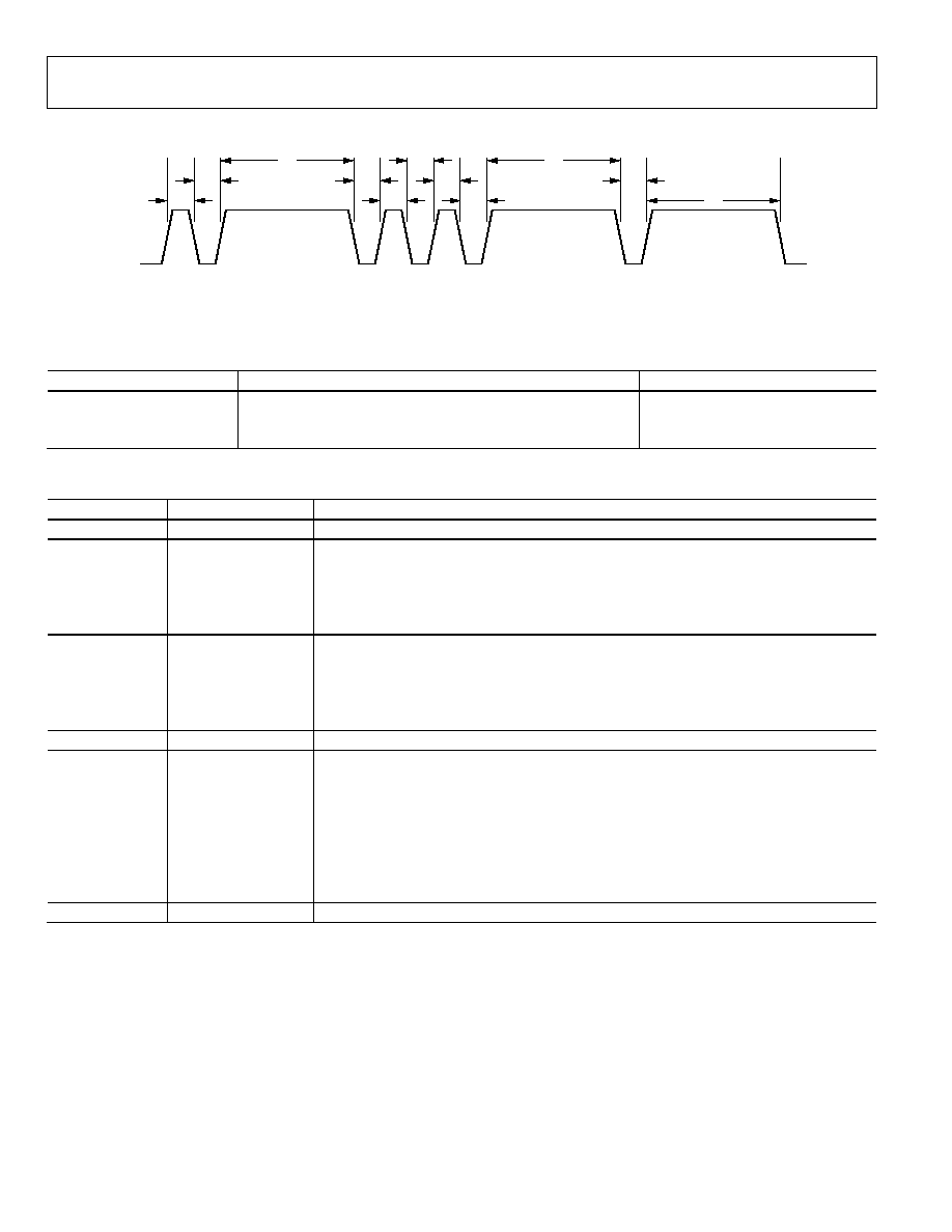
A short pulse at DIGIN from low to high and back to low again,
e.g., between 50 ns and 10 µs long, loads a 0 into a shift register.
A long pulse at DIGIN, e.g., 50 µs or longer, loads a 1 into the
shift register. The time between pulses should be at least 10 µs.
Assuming VSS = 0 V, voltages at DIGIN between VSS and 0.2 ×
VDD are recognized as a low, and voltages at DIGIN between
0.8 × VDD and VDD are recognized as a high. A timing dia-
gram example showing the waveform for entering code 010011
into the shift register is shown in Figure 51.
AD8555
Rev. 0 | Page 20 of 28
04598-0-003
CODE
0
1
0
0
1
1
WAVEFORM
t
W0
t
WS
t
W0
t
WS
t
WS
t
WS
t
W0
t
WS
t
W1
t
W1
t
W1
Figure 51. Timing Diagram for Code 010011
Table 10. Timing Specifications
Timing Parameter
Description
Specification
t
w0
Pulse Width for Loading 0 into Shift Register
Between 50 ns and 10 µs
t
w1
Pulse Width for Loading 1 into Shift Register
50 µs
t
ws
Width between Pulses
10 µs
Table 11. 38-Bit Serial Word Format
Field No.
Bits
Description
Field 0
Bits 0 to 11
12-Bit Start of Packet 1000 0000 0001
Field 1
Bits 12 to 13
2-Bit Function
00: Change Sense Current
01: Simulate Parameter Value
10: Program Parameter Value
11: Read Parameter Value
Field 2
Bits 14 to 15
2-Bit Parameter
00: Second Stage Gain Code
01: First Stage Gain Code
10: Output Offset Code
11: Other Functions
Field 3
Bits 16 to 17
2-Bit Dummy 10
Field 4
Bits 18 to 25
8-Bit Value
Parameter 00 (Second Stage Gain Code): 3 LSBs Used
Parameter 01 (First Stage Gain Code): 7 LSBs Used
Parameter 10 (Output Offset Code): All 8 Bits Used
Parameter 11 (Other Functions)
Bit 0 (LSB): Master Fuse
Bit 1: Fuse for Production Test at Analog Devices
Bit 2: Parity Fuse
Field 5
Bits 26 to 37
12-Bit End of Packet 0111 1111 1110
A 38-bit serial word is used, divided into 6 fields. Assuming
each bit can be loaded in 60 µs, the 38-bit serial word transfers
in 2.3 ms. Table 11 summarizes the word format.
Fields 0 and 5 are the start of packet and end of packet field,
respectively. Matching the start of packet field with 1000 0000
0001 and the end of packet field with 0111 1111 1110 ensures
that the serial word is valid and enables decoding of the other
fields. Field 3 breaks up the data and ensures that no data com-
bination can inadvertently trigger the start of packet and end of
packet fields. Field 0 should be written first and Field 5 written
last. Within each field, the MSB must be written first and the
LSB written last. The shift register features power-on reset to
minimize the risk of inadvertent programming; power-on reset
occurs when VDD is between 0.7 V and 2.2 V.

AD8555
Rev. 0 | Page 21 of 28
Initial State
Initially, all the polysilicon fuses are intact. Each parameter has
the value 0 assigned (see Table 12).
Table 12. Initial State before Programming
Second Stage Gain Code = 0
Second Stage Gain = 17.5
First Stage Gain Code = 0
First Stage Gain = 4.0
Output Offset Code = 0
Output Offset = VSS
Master Fuse = 0
Master Fuse Not Blown
When power is applied to a device, parameter values are taken
either from internal registers if the master fuse is not blown or
from the polysilicon fuses if the master fuse is blown.
Programmed values have no effect until the master fuse is
blown. The internal registers feature power-on reset so that
unprogrammed devices enter a known state after power-up;
power-on reset occurs when VDD is between 0.7 V and 2.2 V.
Simulation Mode
The simulation mode allows any parameter to be changed tem-
porarily. These changes are retained until the simulated value is
reprogrammed, the power is removed, or the master fuse is
blown. Parameters are simulated by setting Field 1 to 01, select-
ing the desired parameter in Field 2, and the desired value for
the parameter in Field 4. Note that a value of 11 for Field 2 is
ignored during the simulation mode. Examples of temporary
settings follow:
·
By setting the second stage gain code (Parameter 00) to 011
and the second stage gain to 50, 1000 0000 0001 01 00 10
0000 0011 0111 1111 1110 is the result.
·
By setting the first stage gain code (Parameter 01) to 000 1011
and the first stage gain to 4.166, 1000 0000 0001 01 01 10
0000 1011 0111 1111 1110 is the result.
A first stage gain of 4.166 with a second stage gain of 50 gives
a total gain of 208.3. This gain has a maximum tolerance of
2.5%.
·
Set the output offset code (Parameter 10) to 0100 0000 and
the output offset to 1.260 V when VDD = 5 V and VSS = 0 V.
This output offset has a maximum tolerance of 0.8%: 1000
0000 0001 01 10 10 0100 0000 0111 1111 1110.
Programming Mode
Intact fuses give a bit value of 0. Bits with a desired value of 1
need to have the associated fuse blown. Since a relatively large
current is needed to blow a fuse, only one fuse can be reliably
blown at a time. Thus, a given parameter value may need several
38-bit words to allow reliable programming. A 5.5 V supply is
required when blowing fuses to minimize the on resistance of
the internal MOS switches that blow the fuse. The power supply
must be able to deliver 250 mA of current, and at least 0.1 µF of
decoupling capacitance is needed across the power pins of the
device. A minimum period of 1 ms should be allowed for each
fuse to blow. There is no need to measure the supply current
during programming; the best way to verify correct program-
ming is to use the read mode to read back the programmed
values and to remeasure the gain and offset to verify these
values. Programmed fuses have no effect on the gain and output
offset until the master fuse is blown; after blowing the master
fuse, the gain and output offset are determined solely by the
blown fuses and the simulation mode is permanently deacti-
vated.
Parameters are programmed by setting Field 1 to 10, selecting
the desired parameter in Field 2, and selecting a single bit with
the value 1 in Field 4.
As an example, suppose the user wants to permanently set the
second stage gain to 50. Parameter 00 needs to have the value
0000 0011 assigned. Two bits have the value 1, so two fuses need
to be blown. Since only one fuse can be blown at a time, the
code 1000 0000 0001 10 00 10 0000 0010 0111 1111 1110 can be
used to blow one fuse. The MOS switch that blows the fuse
closes when the complete packet is recognized and opens when
the start-of-packet, dummy, or end-of-packet fields are no
longer valid. After 1 ms, the second code 1000 0000 0001 10 00
10 0000 0001 0111 1111 1110 can be entered to blow the second
fuse.
To set the first stage gain permanently to a nominal value of
4.151, Parameter 01 needs to have the value 000 1011 assigned.
Three fuses need to be blown, and the following codes can be
used, with a 1 ms delay after each code:
1000 0000 0001 10 01 10 0000 1000 0111 1111 1110
1000 0000 0001 10 01 10 0000 0010 0111 1111 1110
1000 0000 0001 10 01 10 0000 0001 0111 1111 1110
To set the output offset permanently to a nominal value of
1.260 V when VDD = 5 V and VSS = 0 V, Parameter 10 needs to
have the value 0100 0000 assigned. One fuse needs to be blown,
and the following code can be used: 1000 0000 0001 10 10 10
0100 0000 0111 1111 1110.
Finally, to blow the master fuse to deactivate the simulation
mode and prevent further programming, the code 1000 0000
0001 10 11 10 0000 0001 0111 1111 1110 can be used.
There are a total of 20 programmable fuses. Since each fuse
requires 1 ms to blow, and each serial word can be loaded in
2.3 ms, the maximum time needed to program the fuses can be as
low as 66 ms.
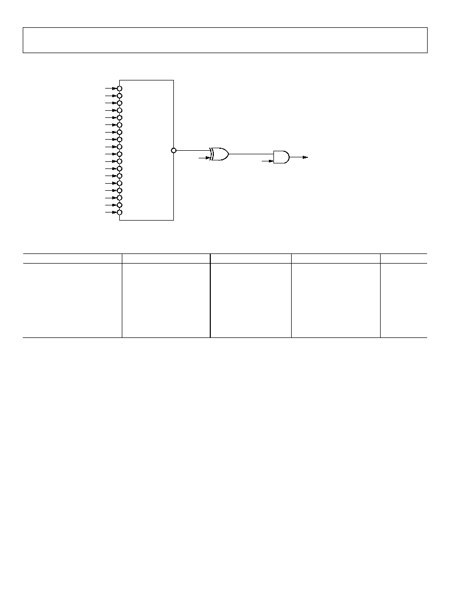
Parity Error Detection
A parity check is used to determine whether the programmed
data of an AD8555 is valid, or whether data corruption has
occurred in the nonvolatile memory. Figure 52 shows the sche-
matic implemented in the AD8555.
AD8555
Rev. 0 | Page 22 of 28
IN01
IN02
IN03
IN04
IN05
IN06
IN07
IN08
IN09
IN10
IN11
IN12
IN13
IN14
IN15
IN16
IN17
IN18
VA0
VA1
VA2
VB0
VB1
VB2
VB3
VB4
VB5
VB6
VC0
VC1
VC2
VC3
VC4
VC5
VC6
VC7
EOR18
OUT
I0
DOT_SUM
PAR_SUM
PFUSE
MFUSE
IN1
IN2
EOR2
AND2
IN1
IN2
PARITY_ERROR
I1
OUT
I2
OUT
04598-0-004
Figure 52. Functional Circuit of AD8555 Parity Check
Table 13. Examples of DAT_SUM
Second Stage Gain Code
First Stage Gain Code
Output Offset Code
Number of Bits with 1
DAT_SUM
000
000 0000
0000 0000
0
0
000
000 0000
1000 0000
1
1
000
000 0000
1000 0001
2
0
000
000 0001
0000 0000
1
1
000
100 0001
0000 0000
2
0
001
000 0000
0000 0000
1
1
001
000 0001
1000 0000
3
1
111
111 1111
1111 1111
18
0
VA0 to VA2 is the 3-bit control signal for the second stage gain,
VB0 to VB6 is the 7-bit control signal for the first stage gain,
and VC0 to VC7 is the 8-bit control signal for the output offset.
PFUSE is the signal from the parity fuse, and MFUSE is the
signal from the master fuse.
The function of the 2-input AND gate (cell and2) is to ignore
the output of the parity circuit (signal PAR_SUM) when the
master fuse has not been blown. PARITY_ERROR is set to 0
when MFUSE = 0. In the simulation mode, for example, parity
check is disabled. After the master fuse has been blown, i.e.,
after the AD8555 has been programmed, the output from the
parity circuit (signal PAR_SUM) is fed to PARITY_ERROR.
When PARITY_ERROR is 0, the AD8555 behaves as a pro-
grammed amplifier. When PARITY_ERROR is 1, a parity error
has been detected, and VOUT is connected to VSS.
The 18-bit data signal (VA0 to VA2, VB0 to VB6, and VC0 to
VC7) is fed to an 18-input exclusive-OR gate (Cell EOR18). The
output of Cell EOR18 is the signal DAT_SUM. DAT_SUM = 0 if
there is an even number of 1s in the 18-bit word; DAT_SUM =
1 if there is an odd number of 1s in the 18-bit word. Examples
are given in Table 13.

AD8555
Rev. 0 | Page 23 of 28
After the second stage gain, first stage gain, and output offset
have been programmed, DAT_SUM should be computed and
the parity bit should be set equal to DAT_SUM. If DAT_SUM is
0, the parity fuse should not be blown in order for the PFUSE
signal to be 0. If DAT_SUM is 1, the parity fuse should be blown
to set the PFUSE signal to 1. The code to blow the parity fuse is
1000 0000 0001 10 11 10 0000 0100 0111 1111 1110.
After setting the parity bit, the master fuse can be blown to pre-
vent further programming, using the code 1000 0000 0001 10 11
10 0000 0001 0111 1111 1110.
Signal PAR_SUM is the output of the 2-input exclusive-OR
gate (Cell EOR2). After the master fuse has been blown,
PARITY_ERROR is set to PAR_SUM. As mentioned earlier,
the AD8555 behaves as a programmed amplifier when
PARITY_ERROR = 0 (no parity error). On the other hand,
VOUT is connected to VSS when a parity error has been
detected, i.e., when PARITY_ERROR = 1.
Read Mode
The values stored by the polysilicon fuses can be sent to the
FILT/DIGOUT pin to verify correct programming. Normally,
the FILT/DIGOUT pin is connected to only the second gain
stage output via RF. During read mode, however, the
FILT/DIGOUT pin is also connected to the output of a shift
register to allow the polysilicon fuse contents to be read. Since
VOUT is a buffered version of FILT/DIGOUT, VOUT also out-
puts a digital signal during read mode.
Read mode is entered by setting Field 1 to 11 and selecting the
desired parameter in Field 2; Field 4 is ignored. The parameter
value, stored in the polysilicon fuses, is loaded into an internal
shift register, and the MSB of the shift register is connected to
the FILT/DIGOUT pin. Pulses at DIGIN shift the shift register
contents out to the FILT/DIGOUT pin, allowing the 8bit
parameter value to be read after seven additional pulses; shift-
ing occurs on the falling edge of DIGIN. An eighth pulse at
DIGIN disconnects FILT/DIGOUT from the shift register and
terminates the read mode. If a parameter value is less than 8 bits
long, the MSBs of the shift register are padded with 0s.
For example, to read the second stage gain, the code 1000 0000
0001 11 00 10 0000 0000 0111 1111 1110 can be used. Since the
second stage gain parameter value is only three bits long, the
FILT/DIGOUT pin has a value of 0 when this code is entered
and remains 0 during four additional pulses at DIGIN. The
fifth, sixth, and seventh pulse at DIGIN returns the 3-bit value
at FILT/DIGOUT, the seventh pulse returning the LSB. An
eighth pulse at DIGIN terminates the read mode.
Sense Current
A sense current is sent across each polysilicon fuse to determine
whether it has been blown or not. When the voltage across the
fuse is less than approximately 1.5 V, the fuse is considered not
blown and Logic 0 is output from the OTP cell. When the volt-
age across the fuse is greater than approximately 1.5 V, the fuse
is considered blown and Logic 1 is output.
When the AD8555 is manufactured, all fuses have a low resis-
tance. When a sense current is sent through the fuse, a voltage
less than 0.1 V is developed across the fuse. This is much lower
than 1.5 V, so Logic 0 is output from the OTP cell. When a fuse
is electrically blown, it should have a very high resistance. When
the sense current is applied to the blown fuse, the voltage across
the fuse should be larger than 1.5 V, so Logic 1 is output from
the OTP cell.
It is theoretically possible (though very unlikely) for a fuse
to be incompletely blown during programming, assuming the
required conditions are met. In this situation, the fuse could
have a medium resistance (neither low nor high), and a voltage
of approximately 1.5 V could be developed across the fuse.
Thus, the OTP cell could sometimes output Logic 0 or a Logic 1,
depending on temperature, supply voltage, and other variables.
To detect this undesirable situation, the sense current can be
lowered by a factor of 4 using a special code. The voltage devel-
oped across the fuse would then change from 1.5 V to 0.38 V,
and the output of the OTP would be a Logic 0 instead of the
Logic 1 expected from a blown fuse. Correctly blown fuses
would still output a Logic 1. In this way, incorrectly blown fuses
can be detected. Another special code would return the sense
current to the normal (larger) value. The sense current cannot
be permanently programmed to the low value. When the
AD8555 is powered up, the sense current defaults to the high
value.
The code to use the low sense current is 1000 0000 0001 00 00
10 XXXX XXX1 0111 1111 1110.
The code to use the normal (high) sense current is 1000 0000
0001 00 00 10 XXXX XXX0 0111 1111 1110.

AD8555
Rev. 0 | Page 24 of 28
Suggested Programming Procedure
1.
Set VDD and VSS to the desired values in the application.
Use simulation mode to test and determine the desired
codes for the second stage gain, first stage gain, and output
offset. The nominal values for these parameters are shown
in Table 6, Table 7, Equation 1, and Equation 2; the codes
corresponding to these values can be used as a starting
point. However, since actual parameter values for given
codes vary from device to device, some fine tuning is nec-
essary for the best possible accuracy.
One way to choose these values is to set the output offset
to an approximate value, e.g., Code 128 for midsupply, to
allow the required gain to be determined. Then set the sec-
ond stage gain such that the minimum first stage gain
(Code 0) gives a lower gain than required, and the maxi-
mum first stage gain (Code 127) gives a higher gain than
required. After choosing the second stage gain, the first
stage gain can be chosen to fine tune the total gain. Finally,
the output offset can be adjusted to give the desired value.
After determining the desired codes for second stage gain,
first stage gain, and output offset, the device is ready for
permanent programming.
2.
Set VSS to 0 V and VDD to 5.5 V. Use program mode to
permanently enter the desired codes for the second stage
gain, first stage gain, and output offset. Blow the master
fuse to allow the AD8555 to read data from the fuses and
to prevent further programming.
3.
Set VDD and VSS to the desired values in the application.
Use read mode with low sense current followed by high
sense current to verify programmed codes.
4.
Measure gain and offset to verify correct functionality.
Suggested Algorithm to Determine
Optimal Gain and Offset Codes
1.
Determine the desired gain, G
A
(e.g., using measure-
ments).
2a.
Use Table 7 to determine the second stage gain G
2
such
that (4.00 × 1.04) < (G
A
/G
2
) < (6.4/1.04). This ensures
that the first and last codes for the first stage gain are not
used, thereby allowing enough first stage gain codes
within each second stage gain range to adjust for the 3%
accuracy.
2b.
Use simulation mode to set the second stage gain to G
2
.
3a.
Set the output offset to allow the AD8555 gain to be
measured, e.g., use Code 128 to set it to midsupply.
3b.
Use Table 6 or Equation 3 to set the first stage gain code
C
G1
such that the first stage gain is nominally G
A
/G
2
.
3c.
Measure the resulting gain G
B
. G
B
should be within
3% of G
A
.
3d.
Calculate the first stage gain error (in relative terms)
E
G1
= G
B
/G
A
- 1.
3e.
Calculate the error (in the number of the first stage gain
codes) C
EG1
= E
G1
/0.00370.
3f.
Set the first stage gain code to C
G1
- C
EG1
.
3g.
Measure the gain G
C
. G
C
should be closer to G
A
than to G
B
.
3h.
Calculate the error (in relative terms) E
G2
= G
C
/G
A
- 1.
3i.
Calculate the error (in the number of the first stage gain
codes) C
EG2
= E
G2
/0.00370.
3j.
Set the first stage gain code to C
G1
- C
EG1
- C
EG2
. The
resulting gain should be within one code of G
A
.
4a.
Determine the desired output offset O
A
, e.g., using the
measurements.
4b.
Use Equation 1 to set the output offset code C
O1
such
that the output offset is nominally O
A
.
4c.
Measure the output offset O
B
. O
B
should be within
3% of O
A
.
4d.
Calculate the error (in relative terms) E
O1
= O
B
/O
A
- 1.
4e.
Calculate the error (in the number of the output offset
codes) C
EO1
= E
O1
/0.00392.
4f.
Set the output offset code to C
O1
- C
EO1
.
4g.
Measure the output offset O
C
. O
C
should be closer to O
A
than to O
B
.
4h.
Calculate the error (in relative terms) E
O2
= O
C
/O
A
- 1.
4i.
Calculate the error (in the number of the output offset
codes) C
EO2
= E
O2
/0.00392.
4j.
Set the output offset code to C
O1
- C
EO1
- C
EO2
. The
resulting offset should be within one code of O
A
.
AD8555
Rev. 0 | Page 25 of 28
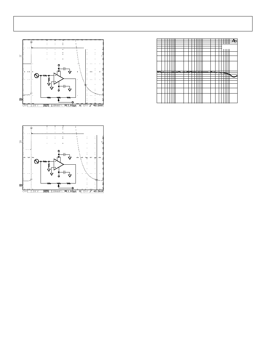
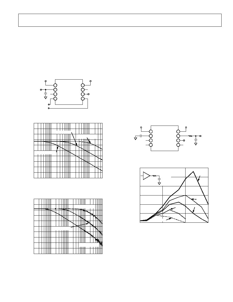
FILTERING FUNCTION
The AD8555's FILT/DIGOUT pin can be used to create a simple
low-pass filter. The AD8555's internal 18 k resistor can be
used with an external capacitor for this purpose. Typical
responses of the AD8555, configured for a gain of 70 and gain
of 1280, are shown in Figure 54 and Figure 55, respectively. This
filtering feature can be used to pass the signals within the filter's
pass band while limiting the out-of-band signals bandwidth
and, therefore, reducing the noise of the overall solution.
1
2
3
4
5
6
7
8
AD8555
VDD
FILT/DIGOUT
DIGIN
VNEG
VSS
VOUT
VCLAMP
VPOS
V
OUT
VDD
C
FILTER
VDD
VSS
04598-0-051
V
IN
Figure 53. AD8555 Configured to Filter Noise
04598-0-052
10
100
1k
10k
50k
dB
40
20
0
C
FILTER
= 0.001
µ
F
C
FILTER
= 0.010
µ
F
C
FILTER
= 0.100
µ
F
Figure 54. Typical Response of the AD8555 at FILT/DIGOUT Pin (Gain = 70)
04598-0-053
100k
10
100
1k
10k
dB
60
40
20
0
C
FILTER
= 0.001
µ
F
C
FILTER
= 0.010
µ
F
C
FILTER
= 0.100
µ
F
Figure 55. Typical Response of the AD8555 at FILT/DIGOUT Pin (Gain = 1280)
DRIVING CAPACITIVE LOADS
The AD8555 can drive large capacitive loads. This feature is
useful when the amplifier, placed close to the sensor, has to
drive long cables. Most instrumentation amplifiers have diffi-
culty driving capacitance due to the degradation of the phase
margin caused by the additional phase lag from the capacitive
load. Higher capacitance at the output can increase the amount
of overshoot and ringing in the amplifier's step response and
could even affect the stability of the device. Additionally, the
value of the capacitive load that an amplifier can drive before
oscillation varies with gain, supply voltage, input signal, and
temperature. Figure 57 and Figure 58 show the overshoot
response of AD8555 versus the capacitive load with a different
value isolation resistor (R
S
) in Figure 56. Similar to all amplifi-
ers, the AD8555 responds with overshoot when driving large C
L
,
but after a point (approximately 22 nF), the overshoot decreases.
This is because the pole created by C
L
dominates at first; how-
ever, at some point, the pole is farther in than the pole setting of
the buffer amplifier and is ignored by AD8555.
1
2
3
4
5
6
7
8
AD8555
VDD
FILT/DIGOUT
DIGIN
VNEG
VSS
VOUT
VCLAMP
VPOS
VDD
C
L
VDD
V
OUT
VSS
04598-0-054
R
S
C
FILTER
Figure 56. Test Circuit for Driving Capacitive Loads
04598-0-028
LOAD CAPACITANCE (nF)
100
0.1
1
10
OVER
SH
OOT (
%
)
60
50
40
30
20
10
0
R
S
C
L
= 1nF
OUTPUT
BUFFER
V
S
= ±2.5V
R
S
= 0
R
S
= 10
R
S
= 20
R
S
= 50
R
S
= 100
Figure 57. Positive Overshoot Graph vs. C
L
AD8555
Rev. 0 | Page 26 of 28
04598-0-029
LOAD CAPACITANCE (nF)
100.0
0.1
1.0
10.0
OVER
SH
OOT (
%
)
60
50
40
30
20
10
0
R
S
C
L
V
S
= ±2.5V
R
S
= 0
R
S
= 10
R
S
= 20
R
S
= 50
R
S
= 100
Figure 58. Negative Overshoot Graph vs. C
L
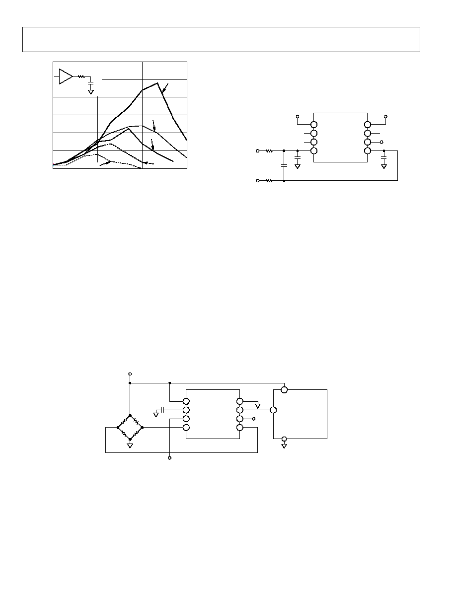
RF INTERFERENCE
All instrumentation amplifiers show dc offset as the result of
rectification of high frequency out-of-band signals that appear
at their inputs. The circuit in Figure 59 provides good RFI sup-
pression without reducing performance within the AD8555 pass
band. Resistor R1 and Capacitor C1, and likewise Resistor R2
and Capacitor C2, form a low-pass RC filter that has a -3 dB
bandwidth equal to f
(-3 dB)
= 1/2 × R1 × C1. It can be seen that
R1, R2 and C1, C2 form a bridge circuit whose output appears
across the amplifier's input pins. Any mismatch between C1, C2
unbalances the bridge and reduce the common-mode rejection.
Using the component values shown, this filter has a bandwidth
of approximately 40 kHz. To preserve common-mode rejection
in the AD8555's pass band, capacitors need to be 5% (silver
mica) or better and should be placed as close to its inputs as
possible. Resistors should be 1% metal film. Capacitor C3 is
needed to maintain common-mode rejection at low frequencies.
This introduces a second low-pass network, R1 + R2 and C3
that has a -3 dB frequency equal to 1/(2 × (R1 + R2)(C3)).
This circuit's -3 dB signal bandwidth is approximately 4 kHz
when a C3 value of 0.047 µF is used (see Figure 59).
1
2
3
4
5
6
7
8
AD8555
VDD
FILT/DIGOUT
DIGIN
VNEG
VSS
VOUT
VCLAMP
VPOS
VPOS
VDD
VDD
VSS
04598-0-057
VNEG
R2
4.02k
R1
4.02k
C3
0.047
µ
F
C2
1nF
C1
1nF
Figure 59. RFI Suppression Method
SINGLE-SUPPLY DATA ACQUISITION SYSTEM
Interfacing bipolar signals to single-supply analog-to-digital
converters (ADCs) presents a challenge. The bipolar signal must
be mapped into the input range of the ADC. Figure 60 shows
how this translation can be achieved. The output offset can be
programmed to a desirable level to accommodate the input
voltage requirement of the ADC.
1
2
3
4
5
6
7
8
AD8555
VDD
FILT/DIGOUT
DIGIN
VNEG
2
4
AD7476
12 BIT
AIN
V
DD
VSS
VOUT
VCLAMP
VPOS
VDD
04598-0-058
VDD
S
DIGIN
10nF
0
100
100
100
100
Figure 60. A Single-Supply Data Acquisition Circuit Using the AD8555
AD8555
Rev. 0 | Page 27 of 28
The bridge circuit with a sensitivity of 2 mV/V is excited by a
5 V supply. The full-scale output voltage from the bridge
(±10 mV) therefore has a common-mode level of 2.5 V. The
AD8555 removes the common-mode component and amplifies
the input signal by a factor of 200 (G1 = 4, G2 = 50, Offset =
128). This results in an output signal of ±2.0 V. In order to pre-
vent this signal from running into the AD8555's ground rail, the
output offset voltage has to be raised to 2.5 V. This signal is
within the input voltage range of the ADC.
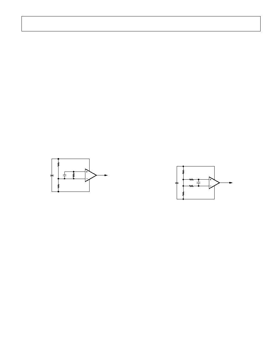
USING THE AD8555 WITH CAPACITIVE SENSORS
Figure 61 shows a crude way of using the AD8555 with capaci-
tive sensors. R
P1
and R
P2
are resistors implementing a potential
divider to bias VNEG to VDD/2. Recommended values range
from 1 k to 1 M. C
S
is the capacitive sensor, and R
S
is a shunt
resistor used to prevent leakage currents from integrating on
the sensor. The value of R
S
is application specific.
Note that although VNEG is tied to a dc voltage, the only
impedance across the capacitive sensor is R
S
. Therefore, the only
way for charge to leak away from C
S
is through R
S
, assuming the
input bias currents at VPOS and VNEG are negligible.
R
S
C
S
R
P2
R
P1
AD8555
VOUT
VDD
VPOS
VNEG
04598-0-059
Figure 61. Crude Way of Using the AD8555 with Capacitive Sensors
The weakness of the circuit in Figure 61 is that the AD8555
input bias current at VPOS flows into R
S
and creates a differen-
tial offset voltage between VPOS and VNEG. This differential
offset voltage is amplified by the AD8555. The input bias cur-
rent at VNEG, on the other hand, flows into R
P1
and create a
common-mode shift. This has little impact on VOUT. Despite
this weakness, the arrangement in Figure 61 should work if the
user wants to minimize the number of components around the
sensor, and if the error introduced by the input bias current at
VPOS is considered negligible.
If greater accuracy is needed, the circuit in Figure 62 is recom-
mended. R
P1
, R
P2
, and C
S
are the same as in Figure 61; R
P1
and
R
P2
should be between 1 k to 1 M. R
S
in Figure 61 has been
split into two resistors, R
S1
and R
S2
, in Figure 62. Again, the only
way for the capacitive sensor to discharge is through (R
S1
+ R
S2
).
The input bias current at VPOS flows through R
S2
and R
P1
, and
the input bias current at VNEG flows through R
S1
and R
P1
. If R
S1
is made equal to R
S2
and if the input bias currents are equal, the
input bias currents give a common-mode shift at VPOS and
VNEG with no differential offset. This common-mode shift is
attenuated by the AD8555 common-mode rejection. Further-
more, changes in input bias current, e.g., with temperature,
manifest as an input common-mode change, also rejected by the
AD8555.
C
S
R
S2
R
P2
R
S1
R
P1
AD8555
VOUT
VDD
VPOS
VNEG
04598-0-060
Figure 62. Recommended Way of Using the AD8555 with Capacitive Sensors
AD8555
Rev. 0 | Page 28 of 28
OUTLINE DIMENSIONS
0.25 (0.0098)
0.17 (0.0067)
1.27 (0.0500)
0.40 (0.0157)
0.50 (0.0196)
0.25 (0.0099)
×
45°
8°
0°
1.75 (0.0688)
1.35 (0.0532)
SEATING
PLANE
0.25 (0.0098)
0.10 (0.0040)
4
1
8
5
5.00 (0.1968)
4.80 (0.1890)
4.00 (0.1574)
3.80 (0.1497)
1.27 (0.0500)
BSC
6.20 (0.2440)
5.80 (0.2284)
0.51 (0.0201)
0.31 (0.0122)
COPLANARITY
0.10
CONTROLLING DIMENSIONS ARE IN MILLIMETERS; INCH DIMENSIONS
(IN PARENTHESES) ARE ROUNDED-OFF MILLIMETER EQUIVALENTS FOR
REFERENCE ONLY AND ARE NOT APPROPRIATE FOR USE IN DESIGN
COMPLIANT TO JEDEC STANDARDS MS-012AA
Figure 63. 8-Lead Standard Small Outline Package [SOIC] Narrow Body
(R-8)
Dimensions shown in millimeters (inches)
16
5
13
8
9
12
1
4
BOTTOM
VIEW
2.25
2.10 SQ
1.95
0.75
0.60
0.50
0.65 BSC
1.95 BSC
0.35
0.28
0.25
12° MAX
0.20 REF
SEATING
PLANE
PIN 1
INDICATOR
TOP
VIEW
4.0
BSC SQ
3.75
BSC SQ
0.60 MAX
0.60 MAX
0.05 MAX
0.02 NOM
0.80 MAX
0.65 TYP
PIN 1
INDICATOR
1.00
0.85
0.80
COPLANARITY
0.08
0.25 MIN
COMPLIANT TO JEDEC STANDARDS MO-220-VGGC
Figure 64. 16-Lead Lead Frame Chip Scale Package [LFCSP] 4 mm × 4 mm Body
(CP-16)
Dimensions shown in millimeters
ORDERING GUIDE
Model
Temperature Range
Package Description
Package Option
AD8555AR
-40°C to +125°C
8-Lead SOIC
R-8
AD8555AR-REEL
-40°C to +125°C
8-Lead SOIC
R-8
AD8555AR-REEL7
-40°C to +125°C
8-Lead SOIC
R-8
AD8555AR-EVAL
Evaluation
Board
AD8555ACP-R2
-40°C to +125°C
16-Lead LFCSP
CP-16
AD8555ACP-REEL
-40°C to +125°C
16-Lead LFCSP
CP-16
AD8555ACP-REEL7
-40°C to +125°C
16-Lead LFCSP
CP-16
© 2004 Analog Devices, Inc. All rights reserved. Trademarks and
regis-
tered trademarks are the property of their respective owners.
D0459804/04(0)
Document Outline
- FEATURES
- APPLICATIONS
- GENERAL DESCRIPTION
- FUNCTIONAL BLOCK DIAGRAM
- TABLE OF CONTENTS
- þÿ
- þÿ
- þÿ
- þÿ
- þÿ
- þÿ