 | ÐлекÑÑоннÑй компоненÑ: AD8591A | СкаÑаÑÑ:  PDF PDF  ZIP ZIP |
AD8591/92/94 Data Sheet
REV. A
Information furnished by Analog Devices is believed to be accurate and
reliable. However, no responsibility is assumed by Analog Devices for its
use, nor for any infringements of patents or other rights of third parties
which may result from its use. No license is granted by implication or
otherwise under any patent or patent rights of Analog Devices.
a
AD8591/AD8592/AD8594
One Technology Way, P.O. Box 9106, Norwood, MA 02062-9106, U.S.A.
Tel: 781/329-4700
World Wide Web Site: http://www.analog.com
Fax: 781/326-8703
© Analog Devices, Inc., 1999
CMOS Single Supply
Rail-to-Rail Input/Output
Operational Amplifiers with Shutdown
PIN CONFIGURATIONS
6-Lead SOT
(RT Suffix)
6
4
1
2
3
OUT A
IN A
V
V
IN A
5
SD
AD8591
10-Lead SOIC
(RM Suffix)
SDA
SDB
5
6
V
+IN B
4
7
OUT A
IN A
+IN A
V+
OUT B
1
2
3
10
9
8
IN B
AD8592
(Not to Scale)
16-Lead Narrow SOIC
(R Suffix)
TOP VIEW
(Not to Scale)
16
15
14
13
12
11
10
9
1
2
3
4
5
6
7
8
NC = NO CONNECT
OUT A
IN A
V
IN A
IN B
IN B
OUT B
NC
OUT D
IN D
IN D
V
IN C
IN C
OUT C
SD
AD8594
16-Lead TSSOP
(RU Suffix)
NC
SD
OUT A
IN A
IN A
V
IN D
IN D
V
OUT D
1
IN B
IN B
OUT B
IN C
OUT C
+IN C
16
AD8594
1
8
9
NC = NO CONNECT
FEATURES
Single Supply Operation: +2.5 V to +6 V
High Output Current: 250 mA
Extremely Low Shutdown Supply Current: 100 nA
Low Supply Current: 750 A/Amp
Wide Bandwidth: 3 MHz
Slew Rate: 5 V/ s
No Phase Reversal
Very Low Input Bias Current
High Impedance Outputs When in Shutdown Mode
Unity Gain Stable
APPLICATIONS
Mobile Communication Handset Audio
PC Audio
PCMCIA/Modem Line Driving
Battery Powered Instrumentation
Data Acquisition
ASIC Input or Output Amplifier
LCD Display Reference Level Driver
GENERAL DESCRIPTION
The AD8591, AD8592 and AD8594 are single, dual and quad
rail-to-rail input and output single supply amplifiers featuring
250 mA output drive current and a power saving shutdown
mode. The AD8592 includes an independent shutdown func-
tion for each amplifier. When both amplifiers are in shutdown
mode the total supply current is reduced to less than 1
µ
A. The
AD8591 and AD8594 include a single master shutdown func-
tion that reduces total supply current to less than 1
µ
A. All
amplifier outputs are in a high impedance state when in shut-
down mode.
These amplifiers have very low input bias currents, making them
suitable for integrators and diode amplification. Outputs are
stable with virtually any capacitive load. Supply current is less
than 750
µ
A per amplifier in active mode.
Applications for these amplifiers include audio amplification for
portable computers, portable phone headsets, sound ports, sound
cards and set-top boxes. The AD859x family is capable of driving
heavy capacitive loads such as LCD panel reference levels.
The ability to swing rail-to-rail at both the input and output
enables designers to buffer CMOS DACs, ASICs and other
wide output swing devices in single supply systems.
The AD8591, AD8592 and AD8594 are specified over the indus-
trial (40
°
C to +85
°
C) temperature range. The AD8591, single,
is available in the tiny 6-lead SOT package. The AD8592, dual, is
available in the 10-lead
µ
SOIC surface mount package. The
AD8594, quad, is available in 16-lead narrow SOIC and 16-lead
TSSOP packages.

2
REV. A
AD8591/AD8592/AD8594SPECIFICATIONS
ELECTRICAL CHARACTERISTICS
Parameter
Symbol
Conditions
Min
Typ
Max
Units
INPUT CHARACTERISTICS
Offset Voltage
V
OS
25
mV
40
°
C < T
A
< +85
°
C
30
mV
Input Bias Current
I
B
5
50
pA
40
°
C < T
A
< +85
°
C
60
pA
Input Offset Current
I
OS
1
25
pA
40
°
C < T
A
< +85
°
C
30
pA
Input Voltage Range
0
+2.7
V
Common-Mode Rejection Ratio
CMRR
V
CM
= 0 V to +2.7 V
38
45
dB
Large Signal Voltage Gain
A
VO
R
L
= 2 k
, V
O
= +0.3 V to +2.4 V
25
V/mV
Offset Voltage Drift
V
OS
/
T
20
µ
V/
°
C
Bias Current Drift
I
B
/
T
50
fA/
°
C
Offset Current Drift
I
OS
/
T
20
fA/
°
C
OUTPUT CHARACTERISTICS
Output Voltage High
V
OH
I
L
= 10 mA
+2.55
+2.61
V
40
°
C to +85
°
C
+2.5
V
Output Voltage Low
V
OL
I
L
= 10 mA
60
100
mV
40
°
C to +85
°
C
125
mV
Output Current
I
OUT
±
250
mA
Open-Loop Impedance
Z
OUT
f = 1 MHz, A
V
= 1
60
POWER SUPPLY
Power Supply Rejection Ratio
PSRR
V
S
= +2.5 V to +6 V
45
55
dB
Supply Current/Amplifier
I
SY
V
O
= 0 V
1
mA
40
°
C < T
A
< +85
°
C
1.25
mA
Supply Current Shutdown Mode
I
SD
All Amplifiers Shut Down
0.1
1
µ
A
40
°
C < T
A
< +85
°
C
1
µ
A
I
SD1
Amplifier 1 Shut Down (AD8592)
1.4
mA
I
SD2
Amplifier 2 Shut Down (AD8592)
1.4
mA
SHUTDOWN INPUTS
Logic High Voltage
V
INH
40
°
C < T
A
< +85
°
C
+1.6
V
Logic Low Voltage
V
INL
40
°
C < T
A
< +85
°
C
+0.5
V
Logic Input Current
I
IN
40
°
C < T
A
< +85
°
C
1
µ
A
DYNAMIC PERFORMANCE
Slew Rate
SR
R
L
= 2 k
3.5
V/
µ
s
Settling Time
t
S
To 0.01%
1.4
µ
s
Gain Bandwidth Product
GBP
2.2
MHz
Phase Margin
o
67
Degrees
Channel Separation
CS
f = 1 kHz, R
L
= 2 k
65
dB
NOISE PERFORMANCE
Voltage Noise Density
e
n
f = 1 kHz
45
nV/
Hz
f = 10 kHz
30
nV/
Hz
Current Noise Density
i
n
f = 1 kHz
0.05
pA/
Hz
Specifications subject to change without notice.
(V
S
= +2.7 V, V
CM
= +1.35 V, T
A
= +25 C unless otherwise noted)

3
REV. A
AD8591/AD8592/AD8594
ELECTRICAL CHARACTERISTICS
Parameter
Symbol
Conditions
Min
Typ
Max
Units
INPUT CHARACTERISTICS
Offset Voltage
V
OS
2
25
mV
40
°
C < T
A
< +85
°
C
30
mV
Input Bias Current
I
B
5
50
pA
40
°
C < T
A
< +85
°
C
60
pA
Input Offset Current
I
OS
1
25
pA
40
°
C < T
A
< +85
°
C
30
pA
Input Voltage Range
0
+5
V
Common-Mode Rejection Ratio
CMRR
V
CM
= 0 V to +5 V
38
47
dB
Large Signal Voltage Gain
A
VO
R
L
= 2 k
, V
O
= +0.5 V to +4.5 V
15
30
V/mV
Offset Voltage Drift
V
OS
/
T
40
°
C < T
A
< +85
°
C
20
µ
V/
°
C
Bias Current Drift
I
B
/
T
50
fA/
°
C
Offset Current Drift
I
OS
/
T
20
fA/
°
C
OUTPUT CHARACTERISTICS
Output Voltage High
V
OH
I
L
= 10 mA
+4.9
+4.94
V
40
°
C to +85
°
C
+4.85
V
Output Voltage Low
V
OL
I
L
= 10 mA
50
100
mV
40
°
C to +85
°
C
125
mV
Output Current
I
OUT
±
250
mA
Open-Loop Impedance
Z
OUT
f = 1 MHz, A
V
= 1
40
POWER SUPPLY
Power Supply Rejection Ratio
PSRR
V
S
= +2.5 V to +6 V
45
55
dB
Supply Current/Amplifier
I
SY
V
O
= 0 V
1.25
mA
40
°
C < T
A
< +85
°
C
1.75
mA
Supply Current-Shutdown Mode
I
SD
All Amplifiers Shut Down
0.1
1
µ
A
40
°
C < T
A
< +85
°
C
1
µ
A
I
SD1
Amplifier 1 Shut Down (AD8592)
1.6
mA
I
SD2
Amplifier 2 Shut Down (AD8592)
1.6
mA
SHUTDOWN INPUTS
Logic High Voltage
V
INH
40
°
C < T
A
< +85
°
C
+2.4
V
Logic Low Voltage
V
INL
40
°
C < T
A
< +85
°
C
+0.8
V
Logic Input Current
I
IN
40
°
C < T
A
< +85
°
C
1
µ
A
DYNAMIC PERFORMANCE
Slew Rate
SR
R
L
= 2 k
5
V/
µ
s
Full-Power Bandwidth
BW
P
1% Distortion
325
kHz
Settling Time
t
S
To 0.01%
1.6
µ
s
Gain Bandwidth Product
GBP
3
MHz
Phase Margin
o
70
Degrees
Channel Separation
CS
f = 1 kHz, R
L
= 10 k
65
dB
NOISE PERFORMANCE
Voltage Noise Density
e
n
f = 1 kHz
45
nV/
Hz
f = 10 kHz
30
nV/
Hz
Current Noise Density
i
n
f = 1 kHz
0.05
pA/
Hz
Specifications subject to change without notice.
(V
S
= +5.0 V, V
CM
= +2.5 V, T
A
= +25 C unless otherwise noted)
AD8591/AD8592/AD8594
4
REV. A
CAUTION
ESD (electrostatic discharge) sensitive device. Electrostatic charges as high as 4000 V readily
accumulate on the human body and test equipment and can discharge without detection. Although
the AD8591/AD8592/AD8594 features proprietary ESD protection circuitry, permanent damage
may occur on devices subjected to high energy electrostatic discharges. Therefore, proper ESD
precautions are recommended to avoid performance degradation or loss of functionality.
ABSOLUTE MAXIMUM RATINGS
1
Supply Voltage . . . . . . . . . . . . . . . . . . . . . . . . . . . . . . . . . +6 V
Input Voltage . . . . . . . . . . . . . . . . . . . . . . . . . . . . . GND to V
S
Differential Input Voltage . . . . . . . . . . . . . . . . . . . . . . . .
±
6 V
Output Short Circuit
Duration to GND
2
. . . . . . . . . . . . Observe Derating Curves
Storage Temperature Range
R, RT, RM, RU Packages . . . . . . . . . . . . 65
°
C to +150
°
C
Operating Temperature Range
AD8591/AD8592/AD8594 . . . . . . . . . . . . 40
°
C to +85
°
C
Junction Temperature Range
R, RT, RM, RU Packages . . . . . . . . . . . . 65
°
C to +150
°
C
Lead Temperature Range (Soldering, 60 sec) . . . . . . . +300
°
C
NOTES
1
Stresses above those listed under Absolute Maximum Ratings may cause perma-
nent damage to the device. This is a stress rating only; functional operation of the
device at these or any other conditions above those listed in the operational sections
of this specification is not implied. Exposure to absolute maximum rating condi-
tions for extended periods may affect device reliability.
2
For supplies less than
±
5 V the differential input voltage is limited to the supplies.
Package Type
JA
1
JC
Units
6-Lead SOT-23 (RT)
230
92
°
C/W
10-Lead
µ
SOIC (RM)
200
44
°
C/W
16-Lead SOIC (R)
120
36
°
C/W
16-Lead TSSOP (RU)
180
35
°
C/W
NOTE
1
JA
is specified for worst case conditions, i.e.,
JA
is specified for device in socket
for surface mount packages.
ORDERING GUIDE
Temperature
Package
Package
Model
Range
Description
Option
AD8591ART
40
°
C to +85
°
C
6-Lead SOT-23
RT-6
AD8592ARM 40
°
C to +85
°
C
10-Lead
µ
SOIC
RM-10
AD8594AR
40
°
C to +85
°
C
16-Lead SOIC
R-16A
AD8594ARU 40
°
C to +85
°
C
16-Lead TSSOP
RU-16
WARNING!
ESD SENSITIVE DEVICE
LOAD CURRENT mA
10
0.1
1k
0.01
OUTPUT VOLTAGE mV
0.1
1
10
1
100
1k
SOURCE
SINK
V
S
= +2.7V
T
A
= +25 C
100
Figure 1. Output Voltage to Supply
Rail vs. Load Current
LOAD CURRENT mA
10
0.1
1k
0.01
OUTPUT VOLTAGE mV
0.1
1
10
1
100
10k
SOURCE
SINK
V
S
= +5V
T
A
= +25 C
100
1k
Figure 2. Output Voltage to Supply
Rail vs. Load Current
TEMPERATURE C
40
20
100
0
20
40
60
80
SUPPLY CURRENT/AMPLIFIER mA
0.90
0.50
0.85
0.70
0.65
0.60
0.55
0.80
0.75
V
S
= +5V
V
S
= +2.7V
Figure 3. Supply Current per
Amplifier vs. Temperature
Typical Performance Characteristics
5
REV. A
AD8591/AD8592/AD8594
SUPPLY VOLTAGE Volts
SUPPLY CURRENT/AMPLIFIER mA
0.8
0.7
0
0.75
1.25
3
1.75
2.25
2.75
0.4
0.3
0.2
0.1
0.6
0.5
T
A
= +25 C
Figure 4. Supply Current per
Amplifier vs. Supply Voltage
TEMPERATURE C
INPUT OFFSET VOLTAGE mV
2
8
50
35
85
5
25
45
65
3
4
5
6
7
V
S
= +5V
V
CM
= +2.5V
15
Figure 5. Input Offset Voltage vs.
Temperature
TEMPERATURE C
INPUT BIAS CURRENT pA
8
2
50
35
85
5
25
45
65
7
6
5
4
3
V
S
= +2.7V, +5V
V
CM
= V
S
/2
15
Figure 6. Input Bias Current vs.
Temperature
TEMPERATURE C
INPUT OFFSET CURRENT pA
4
2
50
35
85
5
25
45
65
3
2
1
0
1
V
S
= +2.7V, +5V
V
CM
= V
S
/ 2
15
Figure 7. Input Offset Current vs.
Temperature
COMMON-MODE VOLTAGE Volts
INPUT BIAS CURRENT pA
8
7
1
0
1
5
2
3
4
5
4
3
2
6
V
S
= +5V
T
A
= +25 C
Figure 8. Input Bias Current vs.
Common-Mode Voltage
FREQUENCY Hz
GAIN dB
80
60
1k
10k
100M
100k
1M
10M
40
0
20
45
90
135
180
PHASE SHIFT Degrees
V
S
= +2.7V
R
L
= NO LOAD
T
A
= +25 C
Figure 9. Open-Loop Gain and Phase
vs. Frequency
FREQUENCY Hz
GAIN dB
80
60
1k
10k
100M
100k
1M
10M
40
0
20
45
90
135
180
PHASE SHIFT De
g
rees
V
S
= +5V
R
L
= NO LOAD
T
A
= +25 C
Figure 10. Open-Loop Gain and
Phase vs. Frequency
FREQUENCY Hz
OUTPUT SWING V p-p
5
4
0
1k
10k
10M
100k
1M
3
2
1
V
S
= +2.7V
R
L
= 2k
T
A
= +25 C
V
IN
= 2.5V p-p
Figure 11. Closed-Loop Output
Voltage Swing vs. Frequency
FREQUENCY Hz
OUTPUT SWING V p-p
5
4
0
1k
10k
10M
100k
1M
3
2
1
V
S
= +5V
R
L
= 2k
T
A
= +25 C
V
IN
= 4.9V p-p
Figure 12. Closed-Loop Output
Voltage Swing vs. Frequency
AD8591/AD8592/AD8594
6
REV. A
FREQUENCY Hz
IMPEDANCE
80
60
1k
10k
100M
100k
1M
10M
40
0
20
V
S
= +5V
T
A
= +25 C
100
120
140
160
180
200
A
V
= 10
A
V
= 1
Figure 13. Closed-Loop Output
Impedance vs. Frequency
FREQUENCY Hz
CMRR dB
110
90
50
1k
10k
10M
100k
1M
80
70
60
V
S
= +5V
T
A
= +25 C
100
Figure 14. Common-Mode Rejection
Ratio vs. Frequency
FREQUENCY Hz
PSRR dB
80
60
1k
10k
100k
1M
10M
40
0
20
V
S
= +2.5V
T
A
= +25 C
100
100
120
140
20
40
60
+PSRR
PSRR
Figure 15. Power Supply Rejection
Ratio vs. Frequency
FREQUENCY Hz
PSRR dB
80
60
1k
10k
100k
1M
10M
40
0
20
V
S
= +5V
T
A
= +25 C
100
100
120
140
20
40
60
+PSRR
PSRR
Figure 16. Power Supply Rejection
Ratio vs. Frequency
CAPACITANCE pF
SMALL SIGNAL OVERSHOOT %
60
50
0
10
100
10k
1k
30
20
10
40
V
S
= +2.5V
R
L
= 2k
T
A
= +25 C
+OS
OS
Figure 17. Small Signal Overshoot
vs. Load Capacitance
CAPACITANCE pF
SMALL SIGNAL OVERSHOOT %
60
50
0
10
100
10k
1k
30
20
10
40
V
S
= +5V
R
L
= 2k
T
A
= +25 C
+OS
OS
Figure 18. Small Signal Overshoot
vs. Load Capacitance
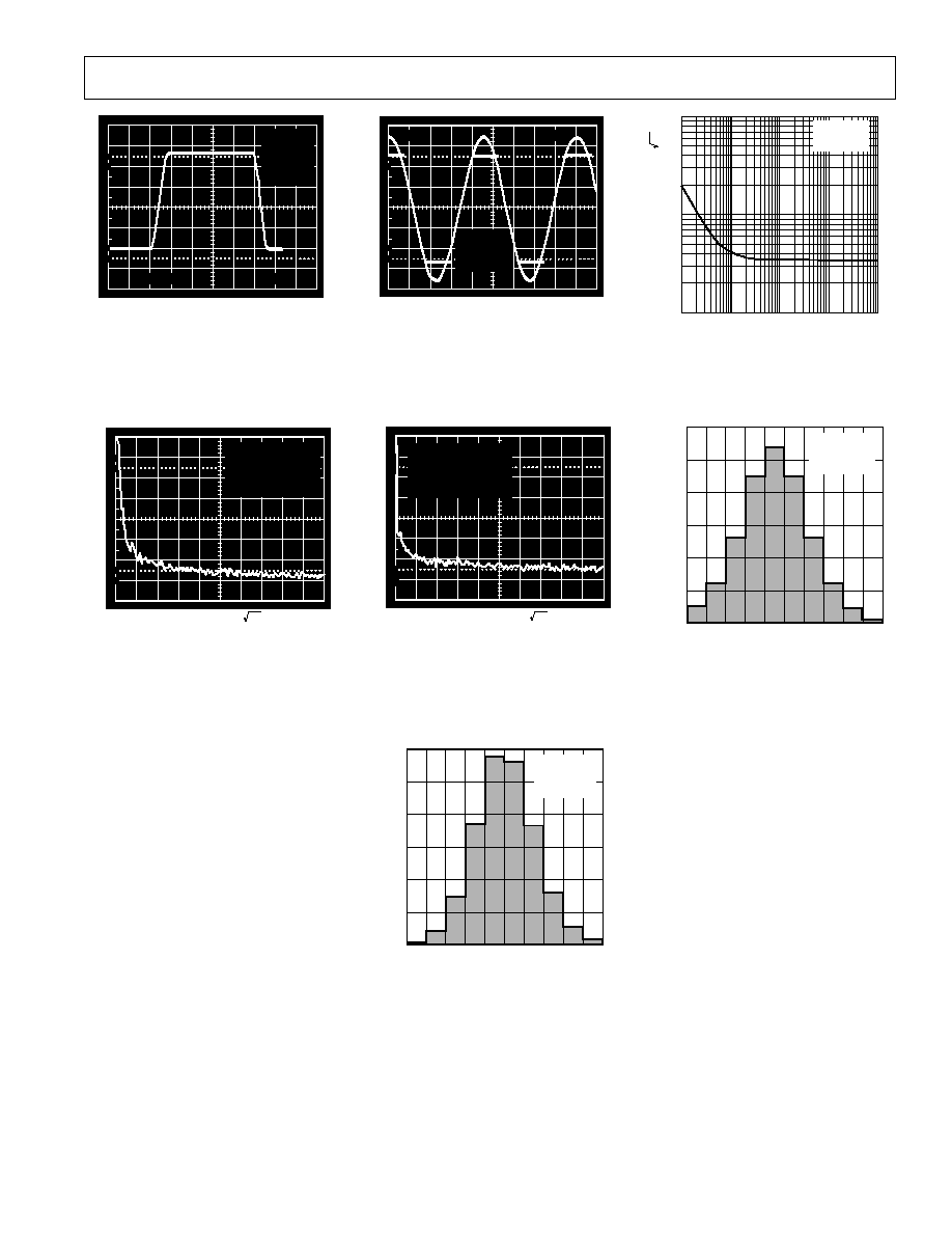
500 ns/DIV
20mV/DIV
V
S
= 1.35V
V
IN
= 50mV
A
V
= 1
R
L
= 2k
C
L
= 300pF
T
A
= +25 C
0V
Figure 19. Small Signal Transient
Response
500 ns/DIV
20mV/DIV
V
S
= 2.5V
V
IN
= 50mV
A
V
= 1
R
L
= 2k
C
L
= 300pF
T
A
= +25 C
0V
Figure 20. Small Signal Transient
Response
10
0%
500ns
500mV
100
90
V
S
= 1.35V
A
V
= 1
R
L
= 2k
T
A
= +25 C
Figure 21. Large Signal Transient
Response
AD8591/AD8592/AD8594
7
REV. A
10
0%
500ns
500mV
100
90
V
S
= 2.5V
A
V
= 1
R
L
= 2k
T
A
= +25 C
Figure 22. Large Signal Transient
Response
10
0%
10 s
1V
100
90
1V
V
S
= 2.5V
A
V
= 1
T
A
= +25 C
Figure 23. No Phase Reversal
FREQUENCY Hz
CURRENT NOISE DENSITY pA/
Hz
1
0.1
0.01
10
100
100k
1k
10k
V
S
= +5V
T
A
= +25 C
Figure 24. Current Noise Density vs.
Frequency
100
90
10
0%
V
S
= +5V
A
V
= 1000
T
A
= +25 C
FREQUENCY = 1kHz
100
V/DIV
MARKER 41 V/
Hz
Figure 25. Voltage Noise Density vs.
Frequency
100
90
10
0%
V
S
= +5V
A
V
= 1000
T
A
= +25 C
FREQUENCY = 10kHz
MARKER 25.9 V/
Hz
200
V/DIV
Figure 26. Voltage Noise Density vs.
Frequency
INPUT OFFSET VOLTAGE mV
QUANTITY Amplifiers
300
500
400
200
100
12 10 8
6
4
2
0
2
4
V
S
= +2.7V
V
CM
= +1.35V
T
A
= +25 C
Figure 27. Input Offset Voltage
Distribution
INPUT OFFSET VOLTAGE mV
QUANTITY Amplifiers
300
12 10 8
6
4
2
0
2
4
500
400
200
100
V
S
= +5V
V
CM
= +2.5V
T
A
= +25 C
Figure 28. Input Offset Voltage
Distribution
AD8591/AD8592/AD8594
8
REV. A
AD8591/AD8592/AD8594 APPLICATION SECTION
Theory of Operation
The AD859x family of amplifiers are all CMOS, high output drive,
rail-to-rail input and output single supply amplifiers designed for
low cost and high output current drive. The parts include a power
saving shutdown function making the AD8591/AD8592/AD8594
op amps ideal for portable multimedia and telecom applications.
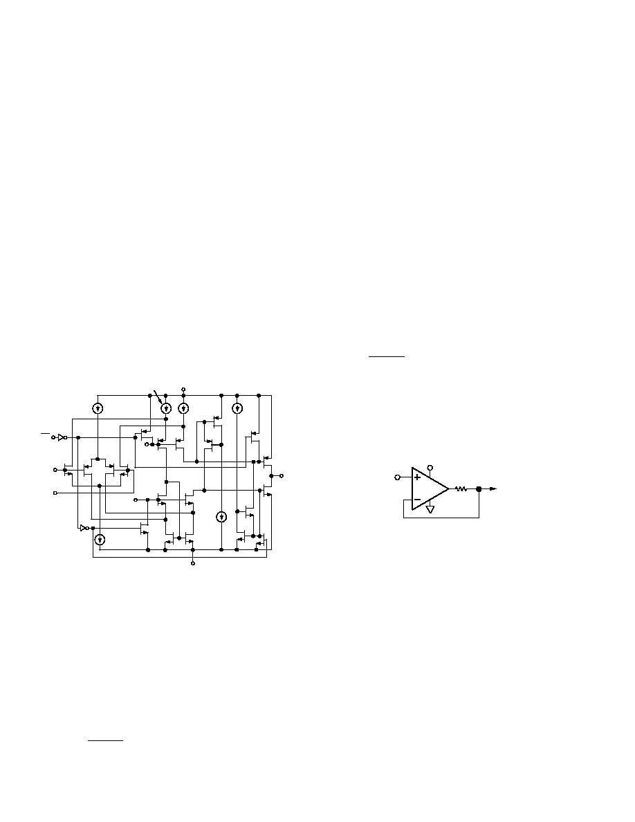
Figure 29 shows the simplified schematic for an AD8591/AD8592/
AD8594 amplifier. Two input differential pairs, consisting of an
n-channel pair (M1-M2) and a p-channel pair (M3-M4), provide
a rail-to-rail input common-mode range. The outputs of the input
differential pairs are combined in a compound folded-cascode
stage, which drives the input to a second differential pair gain
stage. The outputs of the second gain stage provide the gate volt-
age drive to the rail-to-rail output stage.
The rail-to-rail output stage consists of M15 and M16, which are
configured in a complementary common-source configuration.
As with any rail-to-rail output amplifier, the gain of the output
stage, and thus the open-loop gain of the amplifier, is dependent
on the load resistance. Also, the maximum output voltage swing
is directly proportional to the load current. The difference be-
tween the maximum output voltage to the supply rails, known as
the dropout voltage, is determined by the AD8591/AD8592/
AD8594 output transistors' on-channel resistance. The output
dropout voltage is given in Figure 1 and Figure 2.
50 A
100 A
100 A
20 A
V
B2
M5
M8
M12
M15
M16
M11
OUT
M3
M4
M1
IN
IN+
V
B3
M6
M7
M10
20 A
M13
50 A
V+
V
M9
M14
M2
*
*
*
*
M337
SD
INV
*
*
M340
*NOTE: ALL CURRENT SOURCES GO
TO 0 A IN SHUTDOWN MODE
INV
M31
M30
Figure 29. AD8591/AD8592/AD8594 Simplified Schematic
Input Voltage Protection
Although not shown on the simplified schematic, ESD protec-
tion diodes are connected from each input to each power supply
rail. These diodes are normally reverse biased, but will turn on
if either input voltage exceeds either supply rail by more than
+0.6 V. Should this condition occur, the input current should
be limited to less than
±
5 mA. This can be done by placing a
resistor in series with the input(s). The minimum resistor value
should be:
R
V
mA
IN
IN MAX
,
5
(1)
Output Phase Reversal
The AD8591/AD8592/AD8594 are immune to output voltage
phase reversal with an input voltage within the supply voltages
of the device. However, if either of the device's inputs exceeds
+0.6 V outside of the supply rails, the output could exhibit
phase reversal. This is due to the ESD protection diodes be-
coming forward biased, thus causing the polarity of the input
terminals of the device to switch.
The technique recommended in the Input Overvoltage Protection
section should be applied in applications where the possibility of
input voltages exceeding the supply voltages exists.
Output Short Circuit Protection
To achieve high output current drive and rail-to-rail performance,
the outputs of the AD859x family do not have internal short cir-
cuit protection circuitry. Although these amplifiers are designed to
sink or source as much as 250 mA of output current, shorting the
output directly to the positive supply could damage or destroy the
device. To protect the output stage, the maximum output current
should be limited to
±
250 mA.
By placing a resistor in series with the output of the amplifier as
shown in Figure 30, the output current can be limited. The
minimum value for R
X
can be found from Equation 2.
R
V
mA
X
SY
250
(2)
For a +5 V single supply application, R
X
should be at least 20
.
Because R
X
is inside the feedback loop, V
OUT
is not affected. The
tradeoff in using R
X
is a slight reduction in output voltage swing
under heavy output current loads. R
X
will also increase the effec-
tive output impedance of the amplifier to R
O
+ R
X
, where R
O
is
the output impedance of the device.
+5V
R
X
20
V
OUT
V
IN
AD8592
Figure 30. Output Short Circuit Protection
Power Dissipation
Although the AD859x family of amplifiers are able to provide
load currents of up to 250 mA, proper attention should be
given to not exceeding the maximum junction temperature for
the device. The equation for finding the junction temperature is
given as:
T
P
T
DISS
A
A
J
J
=
×
+
(3)
Where
T
J
= AD859x junction temperature
P
DISS
= AD859x power dissipation
JA
= AD859x junction-to-ambient thermal resistance
of the package; and
T
A
= The ambient temperature of the circuit
AD8591/AD8592/AD8594
9
REV. A
In any application, the absolute maximum junction temperature
must be limited to +150
°
C. If this junction temperature is ex-
ceeded, the device could suffer premature failure. If the output
voltage and output current are in phase, for example, with a
purely resistive load, the power dissipated by the AD859x can
be found as:
P
I
V
V
ISS
SY
OUT
D
LOAD
=
×
(
)
(4)
Where
I
LOAD
= AD859x output load current
V
SY
= AD859x supply voltage; and
V
OUT
= The output voltage
By calculating the power dissipation of the device and using the
thermal resistance value for a given package type, the maximum
allowable ambient temperature for an application can be found
using Equation 3.
Capacitive Loading
The AD859x exhibits excellent capacitive load driving capabilities
and can drive up to 10 nF directly. Although the device is stable
with large capacitive loads, there is a decrease in amplifier band-
width as the capacitive load increases. Figure 31 shows a graph of
the AD8592 unity gain bandwidth under various capacitive loads.
CAPACITIVE LOAD nF
4
3.5
0
0.01
100
0.1
BANDWIDTH MHz
1
10
2
1.5
1
0.5
3
2.5
V
S
= 2.5V
R
L
= 1k
T
A
= +25 C
Figure 31. Unity Gain Bandwidth vs. Capacitive Load
When driving heavy capacitive loads directly from the AD859x
output, a snubber network can be used to improve transient
response. This network consists of a series R-C connected from
the amplifier's output to ground, placing it in parallel with the
capacitive load. The configuration is shown in Figure 32. Al-
though this network will not increase the bandwidth of the am-
plifier, it will significantly reduce the amount of overshoot, as
shown in Figure 33.
+5V
R
S
5
V
OUT
V
IN
100mV p-p
AD8592
C
L
47nF
C
S
1 F
Figure 32. Configuration for Snubber Network to
Compensate for Capacitive Loads
10
0%
10 s
50mV
100
90
50mV
47nF LOAD
ONLY
SNUBBER
IN CIRCUIT
Figure 33. Snubber Network Reduces Overshoot and
Ringing Caused from Driving Heavy Capacitive Loads
The optimum values for the snubber network should be determined
empirically based on the size of the capacitive load. Table I shows a
few sample snubber network values for a given load capacitance.
Table I. Snubber Networks for Large Capacitive Loads
Load Capacitance
Snubber Network
(C
L
)
(R
S
, C
S
)
0.47 nF
300
, 0.1
µ
F
4.7 nF
30
, 1
µ
F
47 nF
5
, 1
µ
F
A PC-98 Compliant Headphone/Speaker Amplifier
Because of its high output current performance and shutdown
feature, the AD8592 makes an excellent amplifier for driving an
audio output jack in a computer application. Figure 34 shows
how the AD8592 can be interfaced with an AC97 codec to drive
headphones or speakers.
U1-A
R2
2k
4
C1
100 F
+5V
1
10
2
3
5
+5V
V
DD
V
DD
LEFT
OUT
AD1881
(AC97)
RIGHT
OUT
V
SS
R4
20
+5V
R1
100k
7
8
6
9
R5
20
C2
100 F
NOTE: ADDITIONAL PINS
OMITTED FOR CLARITY
U1-B
U1 = AD8592
R3
2k
NC
28
35
36
Figure 34. A PC-98 Compliant Headphone/Line Out Amplifier
When headphones are plugged into the jack, the normalizing con-
tacts disconnect from the audio contacts. This allows the voltage to
the AD8592 shutdown pins to be pulled up to +5 V, activating the
amplifiers. With no plug in the output jack, the shutdown voltage is
pulled to 100 mV through the R1 and R3 + R5 voltage divider.
This powers the AD8592 down when it is not needed, saving
current from the power supply or battery.
AD8591/AD8592/AD8594
10
REV. A
If gain is required from the output amplifier, four additional
resistors should be added as shown in Figure 35. The gain of
the AD8592 can be set as:
A
R
R
V
=
7
6
(5)
U1-A
R2
2k
4
C1
100 F
+5V
1
10
2
3
5
+5V
V
DD
V
DD
LEFT
OUT
AD1881
(AC97)
RIGHT
OUT
V
SS
R4
20
+5V
R1
100k
7
8
6
9
R5
20
C2
100 F
NOTE: ADDITIONAL PINS
OMITTED FOR CLARITY
U1-B
U1 = AD8592
R3
2k
R7
20k
R7
20k
V
REF
R6
10k
R6
10k
A
V
=
= +6dB WITH VALUES SHOWN
R7
R6
NC
38
35
27
36
Figure 35. A PC-98 Compliant Headphone/Line Out
Amplifier With Gain
Input coupling capacitors are not required for either circuit as
the reference voltage is supplied from the AD1881.
R4 and R5 help protect the AD8592 output in case the output
jack or headphone wires accidentally get shorted to ground.
The output coupling capacitors C1 and C2 block dc current
from the headphones and create a high-pass filter with a corner
frequency of:
f
C
R
R
dB
L
3
1
2
1
4
=
+
(
)
(6)
Where R
L
is the resistance of the headphones.
A Combined Microphone and Speaker Amplifier for
Cellphone and Portable Headsets
The dual amplifiers in the AD8592 make an efficient design for
interfacing with a headset containing a microphone and speaker.
Figure 36 demonstrates a simple method for constructing an
interface to a codec.
U1-A
4
+5V
1
10
2
3
5
C2
10 F
U1 = AD8592
7
8
6
9
R5
10k
U1-B
R6
10k
(OPTIONAL)
R4
10k
FROM CODEC
MONO OUT
(OR LEFT OUT)
TO
CODEC
R3
100k
V
REF
FROM CODEC
MIC + SPEAKER
JACK
R1
2.2k
+5V
R2
10k
R8
100k
+5V
C1
0.1 F
NC
(RIGHT OUT)
R7
1k
Figure 36. A Speaker/Mic Headset Amplifier Circuit
U1-A is used as a microphone preamplifier, where the gain of
the preamplifier is set as R3/R2. R1 is used to bias an electret
microphone and C1 blocks any dc voltages from the amplifier.
U1-B is the speaker amplifier, and its gain is set at R5/R4. To
sum a stereo output, R6 should be added, equal in value to R4.
Using the same principle as described in the previous section,
the normalizing contact on the microphone/speaker jack can be
used to put the AD8592 into shutdown when the headset is not
plugged in. The AD8592 shutdown inputs can also be con-
trolled with TTL or CMOS compatible logic, allowing micro-
phone or speaker muting if desired.
An Inexpensive Sample-and-Hold Circuit
The independent shutdown control of each amplifier in the
AD8592 allows a degree of flexibility in circuit design. One par-
ticular application for which this feature is useful is in designing a
sample-and-hold circuit for data acquisition. Figure 37 shows a
schematic of a simple, yet extremely effective sample-and-hold
circuit using a single AD8592 and one capacitor.
V
IN
U1-A
C1
1nF
U1-B
SAMPLE
AND HOLD
OUTPUT
+5V
1
2
3
5
9
8
7
6
SAMPLE
CLOCK
U1 = AD8592
+5V
4
10
Figure 37. An Efficient Sample-and-Hold Circuit
AD8591/AD8592/AD8594
11
REV. A
The U1-A amplifier is configured as a unity gain buffer driving a
1 nF capacitor. The input signal is connected to the noninverting
input, while the sample clock controls the shutdown for that
amplifier. When the sample clock is high, the U1-A amplifier is
active and the output follows V
IN
. Once the sample clock goes
low, U1-A shuts down with the output of the amplifier going to
a high impedance state, holding the voltage on the C1 capacitor.
The U1-B amplifier is used as a unity gain buffer to prevent load-
ing on C1. Because of the low input bias current of the U1-B
CMOS input stage and the high impedance state of the U1-A
output in shutdown, there is very little voltage droop from C1
during the Hold period. This circuit can be used with sample
frequencies as high as 500 kHz and as low as below 1 Hz. Even
lower voltage droop can be achieved for very low sample rates
by increasing the value of C1.
Direct Access Arrangement for PCMCIA Modems
(Telephone Line Interface)
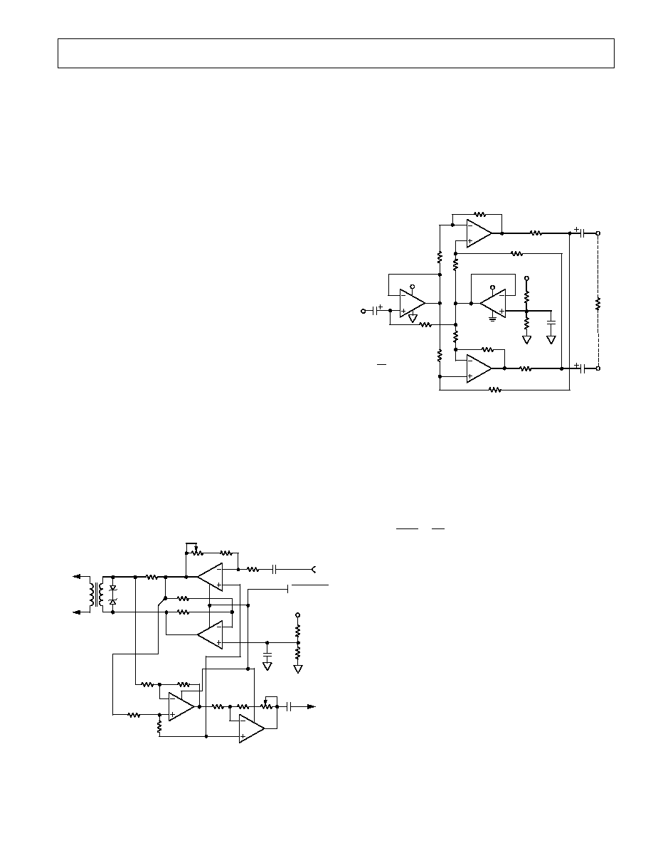
Figure 38 illustrates a +5 V transmit/receive telephone line
interface for 600
systems. It allows full duplex transmission of
signals on a transformer-coupled 600
line in a differential
manner. Amplifier A1 provides gain that can be adjusted to
meet the modem output drive requirements. Both A1 and A2
are configured to apply the largest possible signal on a single
supply to the transformer. Because of the AD8594's high output
current drive and low dropout voltages, the largest signal avail-
able on a single +5 V supply is approximately 4.5 V p-p into a
600
transmission system. Amplifier A3 is configured as a
difference amplifier for two reasons: (1) It prevents the transmit
signal from interfering with the receive signal and (2) it extracts
the receive signal from the transmission line for amplification by
A4. Amplifier A4's gain can be adjusted in the same manner as
A1's to meet the modem's input signal requirements. Standard
resistor values permit the use of SIP (Single In-line Package)
format resistor arrays. Couple this with the AD8594 16-lead
TSSOP or SOIC footprint, and this circuit offers a compact,
cost effective solution.
R7
10k
R8
10k
+5V
6.2V
6.2V
TRANSMIT
TxA
RECEIVE
RxA
C1
0.1 F
R1
10k
R2
9.09k
2k
P1
Tx GAIN
ADJUST
A1
A2
A3
A4
A1, A2 = 1/2 AD8592
A3, A4 = 1/2 AD8592
R3
360
1:1
T1
TO TELEPHONE
LINE
1
2
3
9
8
7
2
3
1
8
7
9
10 F
R5
10k
R6
10k
R9
10k
R14
14.3k
R10
10k
R11
10k
R12
10k
R13
10k
C2
0.1 F
P2
Rx GAIN
ADJUST
2k
Z
O
600
MIDCOM
671-8005
SHUTDOWN
6
5
6
5
Figure 38. A Single Supply Direct Access Arrangement for
PCMCIA Modems
Single Supply Differential Line Driver
Figure 39 shows a single supply differential line driver circuit that
can drive a 600
load with less than 0.7% distortion from 20 Hz
to 15 kHz with an input signal of 4 V p-p and a single +5 V supply.
The design uses an AD8594 to mimic the performance of a fully
balanced transformer based solution. However, this design occu-
pies much less board space while maintaining low distortion and
can operate down to dc. Like the transformer based design, either
output can be shorted to ground for unbalanced line driver applica-
tions without changing the circuit gain of 1.
R
L
600
C1
22 F
A2
9
8
7
3
1
2
A1
+5V
R1
10k
R2
10k
R11
10k
R7
10k
8
7
7
A1
+5V
+5V
R8
100k
R9
100k
C2
1 F
R12
10k
R14
50
A2
1
2
3
R3
10k
R6
10k
R13
10k
C3
47 F
V
O1
V
O2
C4
47 F
A1, A2 = 1/2 AD8592
GAIN = R3
R2
SET: R7, R10, R11 = R2
SET: R6, R12, R13 = R3
V
IN
R10
10k
R5
50
10
4
10
4
9
Figure 39. A Low Noise, Single Supply Differential
Line Driver
R8 and R9 set up the common-mode output voltage equal to
half of the supply voltage. C1 is used to couple the input signal
and can be omitted if the input's dc voltage is equal to half of
the supply voltage.
The circuit can also be configured to provide additional gain if
desired. The gain of the circuit is:
A
V
V
R
R
V
OUT
IN
=
=
3
2
(7)
Where:
V
OUT
= V
O1
V
O2
,
R2 = R7 = R10 = R11 and,
R3 = R6 = R12 = R13

AD8591/AD8592/AD8594
12
REV. A
SPICE Model for the AD8591/AD8592/AD8594 Amplifier
The SPICE model for the AD8591/AD8592/AD8594 amplifier is
one of the more realistic computer simulation macro-models
available, providing a high degree of realism with respect to char-
acteristics of the actual amplifier. This model, shown in Listing 1,
is based on typical values for the device and can be downloaded
from Analog Devices' Internet site at www.analog.com.
The model uses a common source output stage to provide rail-
to-rail performance. This allows realistic simulation of open-
loop gain dependency on load resistance as well as maximum
output voltage versus output current. Two differential pairs are
used in the input stage of the model, simulating the rail-to-rail
input stage of the AD8591/AD8592/AD8594 amplifier.
The EOS voltage source establishes the input offset voltage and
is also used to simulate the common-mode rejection power
supply rejection, and input voltage noise characteristics for the
model. In addition, G2, R2 and CF are used to help set the
open-loop gain and gain-bandwidth product of the model.
A number of secondary characteristics are also accurately por-
trayed in the SPICE model. Flicker noise is accurately modeled
with the 1/f corner frequency set through the KF and AF terms
in the input stage transistors. C1 and C2 are used in the input
section to create secondary poles to achieve an accurate phase
margin characteristic for the model.
The AD8591/AD8592/AD8594 shutdown circuitry is included
in the model. Switches S1 through S7 deactivate the op amp
circuitry in shutdown mode. The logic threshold for the shut-
down circuitry is accurately modeled through the VSWITCH
model parameters near the end of the listing. The active supply
current versus supply voltage is also modeled through the volt-
age-controlled current source GSY.
Characteristics of this model are based on typical values for the
AD8591/AD8592/AD8594 amplifier at +27
°
C. The model's
characteristics are optimized specifically at +27
°
C, and may lose
accuracy at different simulation temperatures.

AD8591/AD8592/AD8594
13
REV. A
Listing 1: AD859x SPICE Macro-Model
* AD8592 SPICE Macro-Model Typical Values
* 9/98, Ver. 1
* TAM / ADSC
*
* Copyright 1998 by Analog Devices
*
* Refer to "README.DOC" file for License
* Statement. Use of this
* model indicates your acceptance of the
* terms and provisions in
* the License Statement.
*
* Node Assignments
*
noninverting input
*
|
inverting input
*
|
|
positive supply
*
|
|
|
negative supply
*
|
|
|
|
output
*
|
|
|
|
|
shutdown
*
|
|
|
|
|
|
.SUBCKT AD8592
1
2
99
50
45
80
*
* INPUT STAGE
*
M1 4 1 3 3 PIX L=0.8E-6 W=125E-6
M2 6 7 3 3 PIX L=0.8E-6 W=125E-6
RC1 4 50 4E3
RC2 6 50 4E3
C1 4 6 2E-12
I1 99 8 100E-6
M3 10 1 12 12 NIX L=0.8E-6 W=125E-6
M4 11 7 12 12 NIX L=0.8E-6 W=125E-6
RC3 10 99 4E3
RC4 11 99 4E3
C2 10 11 2E-12
I2 13 50 100E-6
EOS 7 2 POLY(3) (21,98) (73,98) (61,0)
+1E-3 1 1 1
IOS 1 2 2.5E-12
V1 99 9 0.9
D1 3 9 DX
V2 14 50 0.9
D2 14 12 DX
S1 3 8 (82,98) SOPEN
S2 99 8 (98,82) SCLOSE
S3 12 13 (82,98) SOPEN
S4 13 50 (98,82) SCLOSE
*
* CMRR=64dB, ZERO AT 20kHz
*
ECM1 20 98 POLY(2) (1,98) (2,98) 0 .5 .5
RCM1 20 21 79.6E3
CCM1 20 21 100E-12
RCM2 21 98 50
*
* PSRR=80dB, ZERO AT 200Hz
*
RPS1 70 0 1E6
RPS2 71 0 1E6
CPS1 99 70 1E-5

AD8591/AD8592/AD8594
14
REV. A
CPS2 50 71 1E-5
EPSY 98 72 POLY(2) (70,0) (0,71) 0 1 1
RPS3 72 73 1.59E6
CPS3 72 73 500E-12
RPS4 73 98 80
*
* INTERNAL VOLTAGE REFERENCE
*
EREF 98 0 POLY(2) (99,0) (50,0) 0 .5 .5
GSY 99 50 POLY(1) (99,50) 20E-6 10E-7
*
* SHUTDOWN SECTION
*
E1 81 98 (80,50) 1
R1 81 82 1E3
C3 82 98 1E-9
*
* VOLTAGE NOISE REFERENCE OF 30nV/rt(Hz)
*
VN1 60 0 0
RN1 60 0 16.45E-3
HN 61 0 VN1 30
RN2 61 0 1
*
* GAIN STAGE
*
G2 98 30 POLY(2) (4,6) (10,11) 0 2.19E-5 +2.19E-5
R2 30 98 13E6
CF 45 30 5E-12
S5 30 98 (98,82) SCLOSE
D3 30 31 DX
D4 32 30 DX
V3 99 31 0.6
V4 32 50 0.6
*
* OUTPUT STAGE
*
M5 45 46 99 99 POX L=0.8E-6 W=16E-3
M6 45 47 50 50 NOX L=0.8E-6 W=16E-3
EG1 99 48 POLY(1) (98,30) 1.06 1
EG2 49 50 POLY(1) (30,98) 1.05 1
RG1 48 46 10E3
RG2 49 47 10E3
S6 46 99 (98,82) SCLOSE
S7 47 50 (98,82) SCLOSE
*
* MODELS
*
.MODEL PIX PMOS (LEVEL=2,KP=20E-6,VTO=-0.7, LAMBDA=0.01,AF=1,KF=1E-31)
.MODEL NIX NMOS (LEVEL=2,KP=20E-6,VTO=0.7, LAMBDA=0.01,AF=1,KF=1E-31)
.MODEL POX PMOS (LEVEL=2,KP=8E-6,VTO=-1, LAMBDA=0.067)
.MODEL NOX NMOS (LEVEL=2,KP=13.4E-6,VTO=1, LAMBDA=0.067)
.MODEL SOPEN VSWITCH(VON=2.4,VOFF=0.8, RON=10,ROFF=1E9)
.MODEL SCLOSE VSWITCH(VON=-0.8,VOFF=-2.4, RON=10,ROFF=1E9)
.MODEL DX D(IS=1E-14)
.ENDS AD8592
AD8591/AD8592/AD8594
15
REV. A
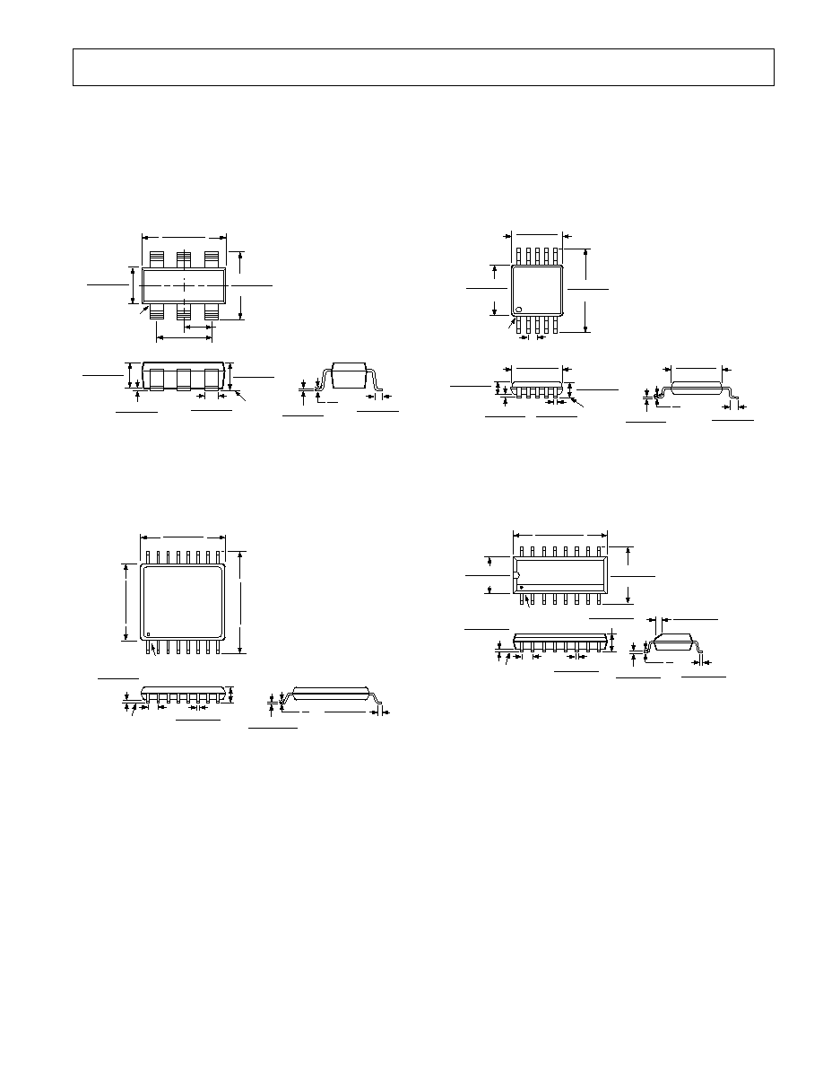
0.199 (5.05)
0.187 (4.75)
1
10
6
5
PIN 1
0.0197 (0.50) BSC
0.124 (3.15)
0.112 (2.84)
0.124 (3.15)
0.112 (2.84)
0.122 (3.10)
0.110 (2.79)
SEATING
PLANE
0.006 (0.15)
0.002 (0.05)
0.016 (0.41)
0.006 (0.15)
0.038 (0.97)
0.030 (0.76)
0.043 (1.09)
0.037 (0.94)
0.011 (0.28)
0.003 (0.08)
0.022 (0.56)
0.021 (0.53)
0.120 (3.05)
0.112 (2.84)
6
0
OUTLINE DIMENSIONS
Dimensions shown in inches and (mm).
6-Lead SOT
(RT-6)
0.122 (3.10)
0.106 (2.70)
PIN 1
0.118 (3.00)
0.098 (2.50)
0.075 (1.90)
BSC
0.037 (0.95) BSC
1
3
4
5
6
2
0.071 (1.80)
0.059 (1.50)
0.009 (0.23)
0.003 (0.08)
0.022 (0.55)
0.014 (0.35)
10
0
0.020 (0.50)
0.010 (0.25)
0.059 (0.15)
0.000 (0.00)
0.051 (1.30)
0.035 (0.90)
SEATING
PLANE
0.057 (1.45)
0.035 (0.90)
16-Lead Thin Shrink Small Outline
(RU-16)
0.177 (4.50)
0.169 (4.30)
16
9
8
1
0.201 (5.10)
0.193 (4.90)
0.256 (6.50)
0.246 (6.25)
PIN 1
SEATING
PLANE
0.006 (0.15)
0.002 (0.05)
0.0118 (0.30)
0.0075 (0.19)
0.0256
(0.65)
BSC
0.0433
(1.10)
MAX
0.0079 (0.20)
0.0035 (0.090)
0.028 (0.70)
0.020 (0.50)
8
0
10-Lead SOIC
(RM-10)
16-Lead Narrow Body SO
(R-16A)
16
9
8
1
0.3937 (10.00)
0.3859 (9.80)
0.2440 (6.20)
0.2284 (5.80)
0.1574 (4.00)
0.1497 (3.80)
PIN 1
SEATING
PLANE
0.0098 (0.25)
0.0040 (0.10)
0.0192 (0.49)
0.0138 (0.35)
0.0688 (1.75)
0.0532 (1.35)
0.0500
(1.27)
BSC
0.0099 (0.25)
0.0075 (0.19)
0.0500 (1.27)
0.0160 (0.41)
8°
0°
0.0196 (0.50)
0.0099 (0.25)
x 45°
15
C3456a02/99
PRINTED IN U.S.A.