 | –≠–ª–µ–∫—Ç—Ä–æ–Ω–Ω—ã–π –∫–æ–º–ø–æ–Ω–µ–Ω—Ç: AD8619 | –°–∫–∞—á–∞—Ç—å:  PDF PDF  ZIP ZIP |
Document Outline
- ˛ˇ
- ˛ˇ
- ˛ˇ
- ˛ˇ
- ˛ˇ
- ˛ˇ
- ˛ˇ
- ˛ˇ
- ˛ˇ
Low Cost Micropower, Low Noise CMOS Rail-to-Rail
Input/Output Operational Amplifiers
AD8617/AD8619
Rev. A
Information furnished by Analog Devices is believed to be accurate and reliable. However, no
responsibility is assumed by Analog Devices for its use, nor for any infringements of patents or other
rights of third parties that may result from its use. Specifications subject to change without notice. No
license is granted by implication or otherwise under any patent or patent rights of Analog Devices.
Trademarks and registered trademarks are the property of their respective owners.
One Technology Way, P.O. Box 9106, Norwood, MA 02062-9106, U.S.A.
Tel: 781.329.4700
www.analog.com
Fax: 781.461.3113
© 2005 Analog Devices, Inc. All rights reserved.
FEATURES
Offset voltage: 2.2 mV max
Low input bias current: 1 pA max
Single-supply operation: 1.8 V to 5 V
Low noise: 22 nV/Hz
Micropower: 40 A max
No phase reversal
Unity gain stable
APPLICATIONS
Battery-powered instrumentation
Multipole filters
Current shunt sense
Sensors
ADC predrivers
DAC drivers/level shifters
Low power ASIC input or output amplifiers
GENERAL DESCRIPTION
The AD8617/AD8619 are dual and quad micropower rail-to-
rail input and output amplifiers that feature low supply current,
low input voltage, and low current noise.
The parts are fully specified to operate from 1.8 V to 5.0 V
single supply, or ±0.9 V and ±2.5 V dual supply. The combination
of low noise, very low input bias currents, and low power
consumption make the AD8617/AD8619 especially useful in
portable and loop-powered instrumentation.
The ability to swing rail-to-rail at both the input and output
enables designers to buffer CMOS ADCs, DACs, ASICs, and
other wide output swing devices in low power, single-supply
systems.
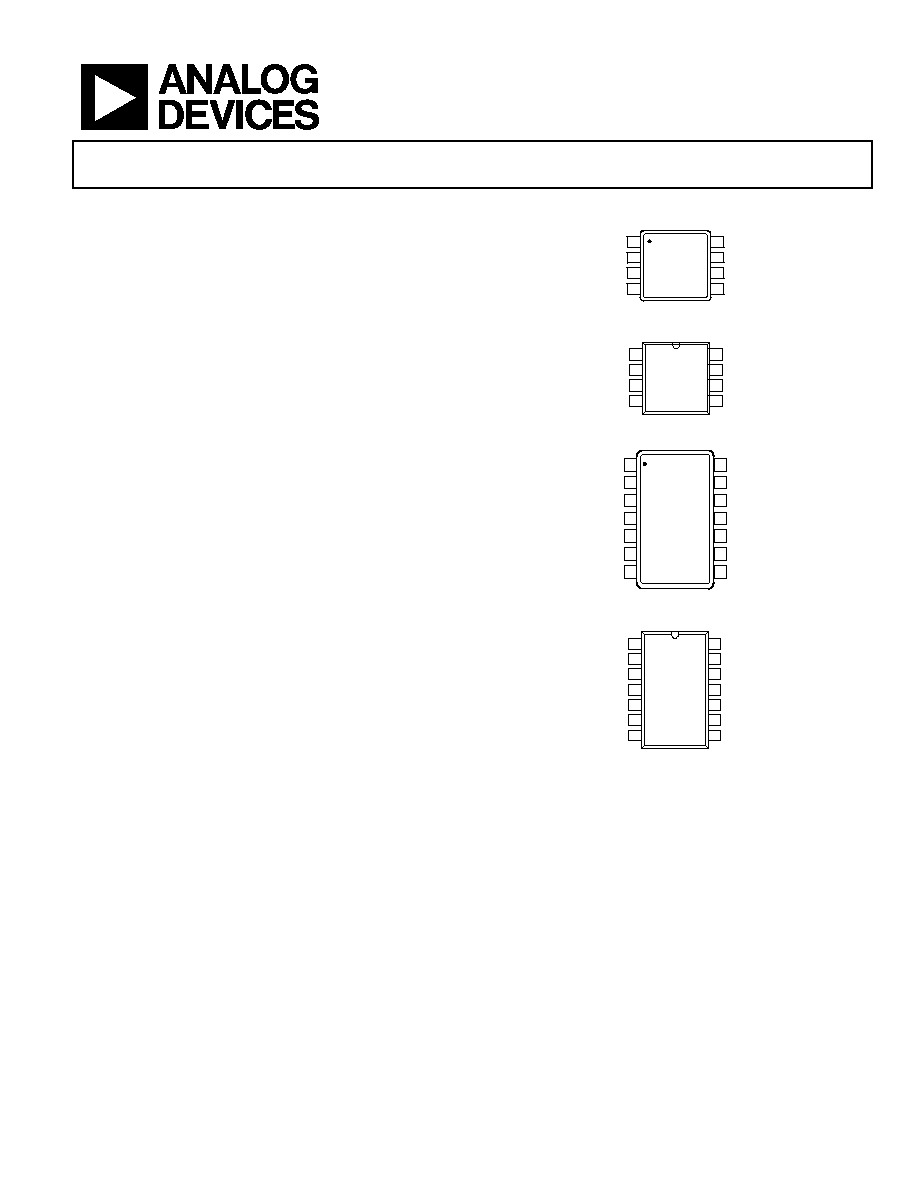
The AD8617 is available in 8-lead MSOP and 8-lead SOIC
packages. The AD8619 is available in 14-lead TSSOP and
14-lead SOIC packages.
PIN CONFIGURATIONS
OUT A
1
≠IN A
2
+IN A
3
V≠
4
V+
8
OUT B
7
≠IN B
6
+IN B
5
AD8617
TOP VIEW
(Not to Scale)
05622-001
Figure 1. 8-Lead MSOP
05622-002
OUT A
1
≠IN A
2
+IN A
3
V≠
4
V+
8
OUT B
7
≠IN B
6
+IN B
5
AD8617
TOP VIEW
(Not to Scale)
Figure 2. 8-Lead SOIC_N
05622-035
1
2
3
4
5
6
7
AD8619
≠IN A
+IN A
V+
OUT B
≠IN B
+IN B
OUT A
14
13
12
11
10
9
8
≠IN D
+IN D
V≠
OUT C
≠IN C
+IN C
OUT D
TOP VIEW
(Not to Scale)
Figure 3. 14-Lead TSSOP
05622-036
OUT A
1
≠IN A
2
+IN A
3
V+
4
OUT D
14
≠IN D
13
+IN D
12
V≠
11
+IN B
5
+IN C
10
≠IN B
6
≠IN C
9
OUT B
7
OUT C
8
AD8619
TOP VIEW
(Not to Scale)
Figure 4. 14-Lead SOIC_N

AD8617/AD8619
Rev. A | Page 2 of 16
TABLE OF CONTENTS
Features .............................................................................................. 1
Applications....................................................................................... 1
General Description ......................................................................... 1
Pin Configurations ........................................................................... 1
Specifications..................................................................................... 3
Absolute Maximum Rating ............................................................. 5
Thermal Resistance ...................................................................... 5
ESD Caution.................................................................................. 5
Typical Performance Characteristics ............................................. 6
Outline Dimensions ....................................................................... 12
Ordering Guide........................................................................... 13
REVISION HISTORY
10/05--Rev. 0 to Rev. A
Added New Part..................................................................Universal
Change to Specifications Section.................................................... 3
Updated Outline Dimensions ....................................................... 12
Changes to Ordering Guide .......................................................... 13
9/05--Revision 0: Initial Version

AD8617/AD8619
Rev. A | Page 3 of 16
SPECIFICATIONS
Electrical characteristics @ V
S
= 5 V, V
CM
= V
S
/2, T
A
= 25∞C, unless otherwise noted.
Table 1.
Parameter
Symbol
Conditions
Min
Typ
Max
Unit
INPUT CHARACTERISTICS
Offset Voltage
V
OS
-0.3 V < V
CM
< +5.3 V
0.4
2.2
mV
-40∞C
<
T
A
< +125∞C, ≠0.3 V < V
CM
< +5.2 V
2.2
mV
Offset Voltage Drift
V
OS
/T -40∞
<
T
A
< +125∞C
1
4.5
V/∞C
Input Bias Current
I
B
0.2
1
pA
-40∞C
<
T
A
< +85∞C
110
pA
-40∞C
<
T
A
< +125∞C
780
pA
Input Offset Current
I
OS
0.1
0.5
pA
-40∞C
<
T
A
< +85∞C
50
pA
-40∞C
<
T
A
< +125∞C
250
pA
Common-Mode Rejection Ratio
CMRR
0 V < V
CM
< 5 V
95
dB
-40∞C
<
T
A
< +125∞C
68
dB
Large Signal Voltage Gain
A
VO
R
L
= 10 k, 0.5 V < V
O
< 4.5 V
235
500
V/mV
Input Capacitance
C
DIFF
1.9
pF
C
CM
2.5
pF
OUTPUT CHARACTERISTICS
Output Voltage High
V
OH
I
L
= 1 mA
4.95
4.98
V
-40∞C to +125∞C
4.9
V
I
L
= 10 mA
4.65
4.7
V
-40∞C to +125∞C
4.50
V
Output Voltage Low
V
OL
I
L
= 1 mA
20
30
mV
-40∞C to +125∞C
50
mV
I
L
= 10 mA
190
275
mV
-40∞C to +125∞C
335
mV
Short-Circuit Current
I
SC
±80
mA
Closed-Loop Output Impedance
Z
OUT
f = 10 kHz, A
V
= 1
15
POWER
SUPPLY
Power Supply Rejection Ratio
PSRR
1.8 V < V
S
< 5 V
67
94
dB
-40∞C
<
T
A
< +125∞C
64
dB
Supply Current/Amplifier
I
SY
V
O
= V
S
/2
38
41
A
-40∞C
<T
A
< +125∞C
50
A
DYNAMIC PERFORMANCE
Slew Rate
SR
R
L
= 10 k
0.1
V/s
Settling Time 0.1%
t
S
G = ±1, 2 V step, C
L
= 20 pF, R
L
= 1 k
23
s
Gain Bandwidth Product
GBP
R
L
= 100 k
400
kHz
R
L
= 10 k
350
kHz
Phase Margin
ÿ
O
R
L
= 10 k, R
L
= 100 k, C
L
= 20 pF
70
Degrees
NOISE PERFORMANCE
Peak-to-Peak Noise
2.3
3.5
V
Voltage Noise Density
e
n
f = 1 kHz
25
nV/Hz
f = 10 kHz
22
nV/Hz
Current Noise Density
i
n
f = 1 kHz
0.05
pA/Hz

AD8617/AD8619
Rev. A | Page 4 of 16
Electrical characteristics @ V
S
= 1.8 V, V
CM
= V
S
/2, T
A
= 25∞C, unless otherwise noted.
Table 2.
Parameter
Symbol
Conditions
Min
Typ
Max
Unit
INPUT CHARACTERISTICS
Offset Voltage
V
OS
-0.3 V < V
CM
< +1.9 V
0.4
2.2
mV
-0.3 V < V
CM
< +1.8 V ; -40∞C < T
A
< +125∞C
2.2
mV
Offset Voltage Drift
V
OS
/T -40∞C
<
T
A
< +125∞C
1
8.5
V/∞C
Input Bias Current
I
B
0.2
1
pA
-40∞C
<
T
A
< +85∞C
110
pA
-40∞C
<
T
A
< +125∞C
780
pA
Input Offset Current
I
OS
0.1
0.5
pA
-40∞C
<
T
A
< +85∞C
50
pA
-40∞C
<
T
A
< +125∞C
250
pA
Common-Mode Rejection Ratio
CMRR
0 V < V
CM
< 1.8 V
86
dB
-40∞C
<
T
A
< +125∞C
55
dB
Large Signal Voltage Gain
A
VO
R
L
= 10 k, 0.5 V < V
O
< 1.3 V
85
1,000
V/mV
Input Capacitance
C
DIFF
2.1
pF
C
CM
3.8
pF
OUTPUT CHARACTERISTICS
Output Voltage High
V
OH
I
L
= 1 mA
1.65
1.73
V
-40∞C to +125∞C
1.6
V
Output Voltage Low
V
OL
I
L
= 1 mA
44
60
mV
-40∞C to +125∞C
80
mV
Short-Circuit Current
I
SC
±7
mA
Closed-Loop Output Impedance
Z
OUT
f = 10 kHz, A
V
= 1
15
POWER SUPPLY
Power Supply Rejection Ratio
PSRR
1.8 V < V
S
< 5 V
67
94
dB
Supply Current/Amplifier
I
SY
V
O
= V
S
/2
38
41
A
-40∞C
<T
A
< +125∞C
50
A
DYNAMIC PERFORMANCE
Slew Rate
SR
R
L
= 10 k
0.1
V/s
Settling Time 0.1%
t
S
G = ±1, 1 V step, C
L
= 20 pF, R
L
= 1 k
6. 5
s
Gain Bandwidth Product
GBP
R
L
= 100 k
400
kHz
R
L
= 10 k
350
kHz
Phase Margin
ÿ
O
R
L
= 10 k, R
L
= 100 k, C
L
= 20 pF
70
Degrees
NOISE PERFORMANCE
Peak-to-Peak Noise
2.3
3.5
V
Voltage Noise Density
e
n
f = 1 kHz
25
nV/Hz
f = 10 kHz
22
nV/Hz
Current Noise Density
i
n
f = 1 kHz
0.05
pA/Hz
AD8617/AD8619
Rev. A | Page 5 of 16
ABSOLUTE MAXIMUM RATING
T
A
= 25∞C, unless otherwise noted.
Table 3.
Parameter Rating
Supply Voltage
+6 V
Input Voltage
V
SS
- 0.3 V to V
DD
+ 0.3 V
Differential Input Voltage
±6 V
Output Short-Circuit Duration to GND
Observe derating curve
Storage Temperature Range
-65∞C to +150∞C
Lead Temperature (Soldering, 60 sec)
300∞C
Operating Temperature Range
-40∞C to +125∞C
Junction Temperature Range
-65∞C to +150∞C
Stresses above those listed under Absolute Maximum Ratings
may cause permanent damage to the device. This is a stress
rating only; functional operation of the device at these or any
other conditions above those indicated in the operational
section of this specification is not implied. Exposure to absolute
maximum rating conditions for extended periods may affect
device reliability.
Absolute maximum ratings apply at 25∞C, unless otherwise
noted.
THERMAL RESISTANCE
JA
is specified for the worst-case conditions, that is, a device
soldered in a circuit board for surface-mount packages.
Table 4. Thermal Characteristics
Package Type
JA
JC
Unit
8-Lead MSOP (RM-8)
210
45
∞C/W
8-Lead SOIC_N (R-8)
158
43
∞C/W
14-Lead SOIC_N (R-14)
120
36
∞C/W
14-Lead TSSOP (RU-14)
180
35
∞C/W
ESD CAUTION
ESD (electrostatic discharge) sensitive device. Electrostatic charges as high as 4000 V readily accumulate on
the human body and test equipment and can discharge without detection. Although this product features
proprietary ESD protection circuitry, permanent damage may occur on devices subjected to high energy
electrostatic discharges. Therefore, proper ESD precautions are recommended to avoid performance
degradation or loss of functionality.
AD8617/AD8619
Rev. A | Page 6 of 16
TYPICAL PERFORMANCE CHARACTERISTICS
V
SY
= 5 V or ±2.5 V, unless otherwise noted.
1800
0
≠2000
1900
05622-003
INPUT OFFSET VOLTAGE (
V)
NUMBE
R OF AMP
LIFIE
RS
1600
1400
1200
1000
800
600
400
200
≠
1700
≠
1400
≠1100
≠800
≠500
≠200
100
400
700
1000
1300
1600
V
SY
= 5.5V
≠0.5V < V
CM
< +5.5V
T
A
= 25∞C
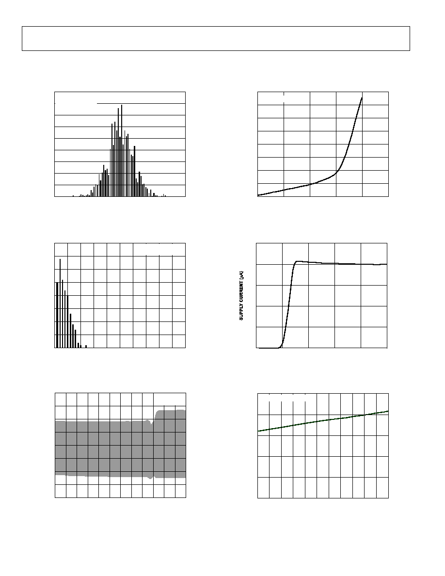
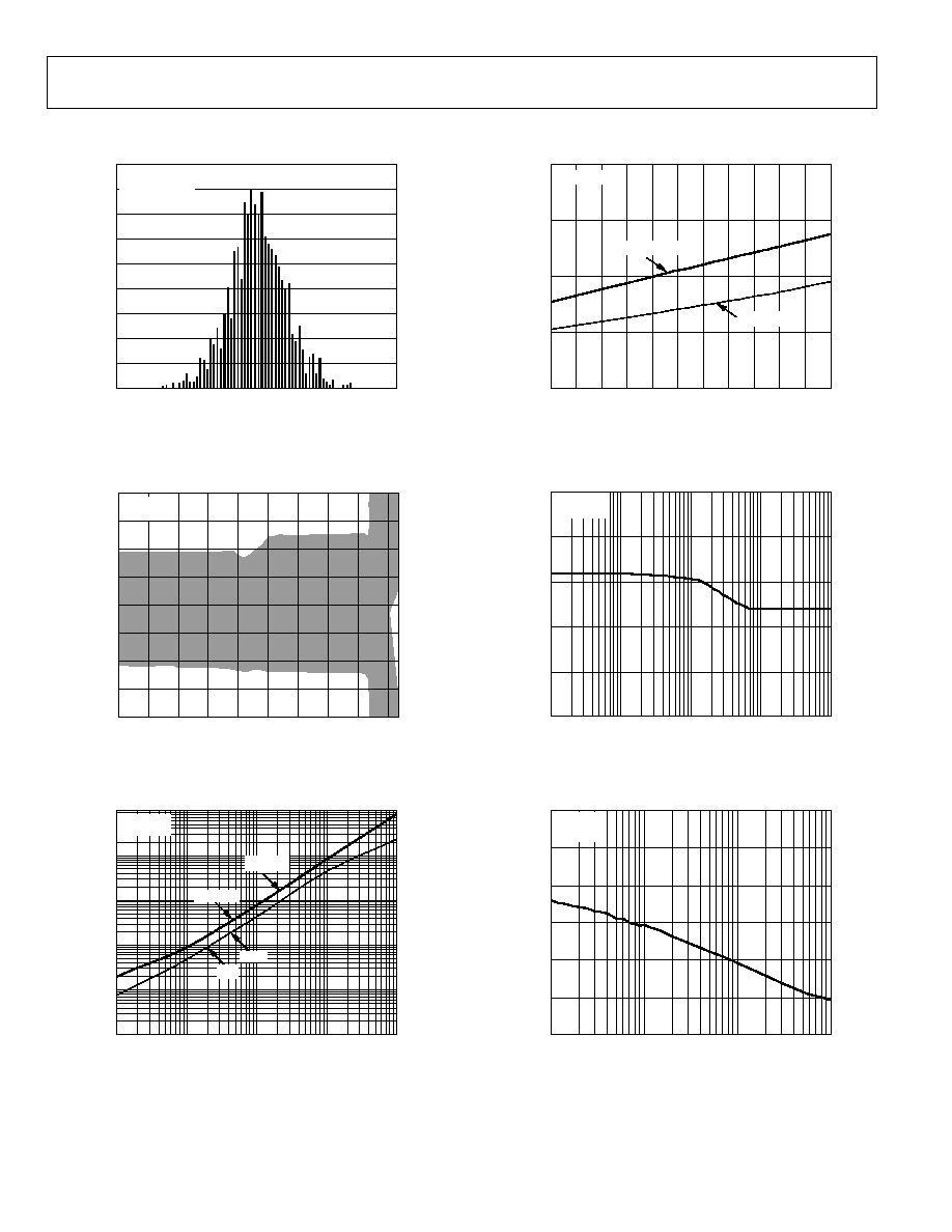
Figure 5. Input Offset Voltage Distribution
40
0
0
10
05622-004
TCV
OS
(
V/∞C)
NUMBE
R OF AMP
LIFIE
RS
35
30
25
20
15
10
5
1
2
3
4
5
6
7
8
9
≠40∞C < T
A
< 125∞C
V
CM
= 2.5V
Figure 6. Input Offset Voltage Drift Distribution
2000
≠2000
≠0.5
5.5
05622-005
INPUT COMMON-MODE VOLTAGE (V)
INPUT OFFSET VOL
T
AGE (
V)
1500
1000
500
0
≠500
≠1000
≠1500
0
0.5 1.0 1.5 2.0 2.5 3.0 3.5 4.0 4.5 5.0
V
SY
= 5V
T
A
= 25∞C
Figure 7. Input Offset Voltage vs. Common-Mode Voltage
400
0
25
150
05622-006
TEMPERATURE (∞C)
INP
U
T BIAS
CURRE
NT (pA)
350
300
250
200
150
100
50
50
75
100
125
V
SY
= 5V AND 1.8V
Figure 8. Input Bias Current vs. Temperature
50
0
0
5
05622-007
SUPPLY VOLTAGE (V)
T
A
= 25∞C
40
30
20
10
1
2
3
4
Figure 9. Supply Current vs. Supply Voltage
50
0
≠40
05622-008
TEMPERATURE (∞C)
S
U
P
P
L
Y
CURRE
NT/AMP
LIFIE
R
(
A)
40
30
20
10
≠10
20
50
80
110
V
SY
= ±2.5V, ±1.35V, ±0.9V
Figure 10. Supply Current vs. Temperature

AD8617/AD8619
Rev. A | Page 7 of 16
1k
0.01
0.001
10
05622-009
LOAD CURRENT (mA)
OUTP
UT S
A
TURATION V
O
LTAGE
(mV
)
0.01
0.1
1
0.1
1
10
100
V
SY
= 5V
T
A
= 25∫C
SOURCE
V
SY
≠ V
OH
SINK
V
OL
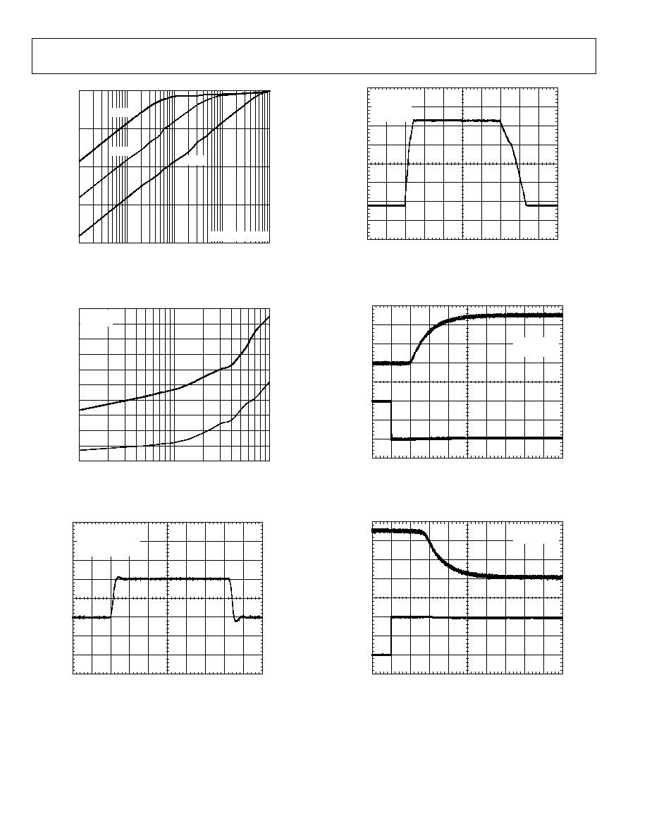
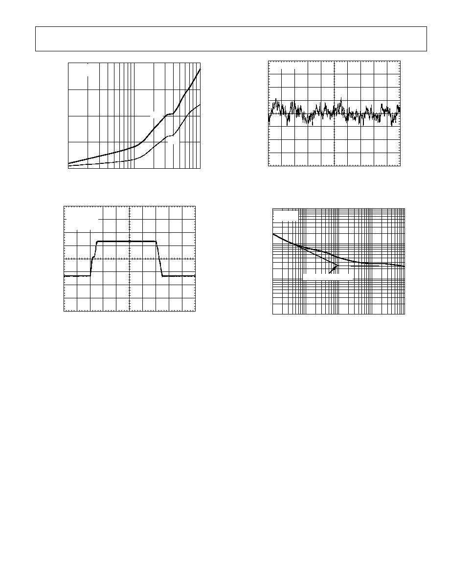
Figure 11. Output Saturation Voltage vs. Load Current
40
0
≠40
125
05622-010
TEMPERATURE (∞C)
OUTP
UT S
A
TURATION V
O
LTAGE
(mV
)
30
20
10
≠25 ≠10
5
20
35
50
65
80
95
110
V
SY
= 5V
V
SY
≠ V
OH
@ 1mA
V
OL
@ 1mA
Figure 12. Output Saturation Voltage vs. Temperature
(I
L
= 1 mA)
350
0
≠40
125
05622-011
TEMPERATURE (∞C)
OUTP
UT S
A
TURATION V
O
LTAGE
(mV
)
≠25 ≠10
5
20
35
50
65
80
95
110
V
SY
= 5V
V
OL
@ 10mA
300
250
200
150
100
50
V
DD
≠ V
OH
@ 10mA
Figure 13. Output Saturation Voltage vs. Temperature
(I
L
= 10 mA)
60
≠20
1k
1M
05622-012
FREQUENCY (Hz)
OPEN-
L
OOP GAIN (
d
B)
≠45
0
45
90
135
OPEN
-
L
OOP PH
A
SE SH
IFT (
D
egrees)
10k
100k
50
40
30
20
10
0
≠10
V
SY
= ±2.5V AND ±0.9V
R
L
= 100k
C
L
= 20pF
M
Figure 14. Open-Loop Gain and Phase vs. Frequency
120
0
100
1M
05622-013
FREQUENCY (Hz)
CMRR (dB)
1k
10k
100
80
60
40
20
100k
V
SY
= 5V AND 2.7V
T
A
= 25∞C
Figure 15. CMRR vs. Frequency
120
0
100
1M
05622-014
FREQUENCY (Hz)
P
S
RR (dB)
1k
10k
100k
100
80
60
40
20
V
SY
= ±2.5V AND ±1.35V
T
A
= 25∞C
Figure 16. PSRR vs. Frequency
AD8617/AD8619
Rev. A | Page 8 of 16
1k
0
100
1M
05622-015
FREQUENCY (Hz)
OUTP
UT IMP
E
DANCE
(
)
1k
10k
100k
100
10
1
V
SY
= 5V AND 1.8V
A
V
= 10
A
V
= 1
A
V
= 100
Figure 17. Closed-Loop Output Impedance vs. Frequency
50
0
10
1000
05622-016
LOAD CAPACITANCE (pF)
SM
A
LL SIGN
A
L
OVER
SH
OOT (
%
)
≠OS
+OS
100
45
40
35
30
25
20
15
10
5
V
SY
= 5V
T
A
= 25∞C
Figure 18. Small Signal Overshoot vs. Load Capacitance
05622-017
TIME (4
s/DIV)
V
SY
= 5V, 2.7V, 1.8V
A
V
= 1
R
L
= 10k
C
L
= 200pF
VOLTA
GE (
50mV/D
IV)
Figure 19. Small Signal Transient Response
05622-018
TIME (20
s/DIV)
V
SY
= 5V
A
V
= 1
R
L
= 10k
C
L
= 200pF
VOLTA
GE (
1
V/D
IV)
Figure 20. Large Signal Transient Response
05622-019
TIME (20
s/DIV)
V
SY
= ±2.5V
A
V
= ≠50
V
OUT
(V
)
V
IN
(mV
)
≠2.5
0
0
100
Figure 21. Positive Overload Recovery
05622-020
TIME (20
s/DIV)
V
SY
= ±2.5V
A
V
= ≠50
V
OUT
(V
)
V
IN
(mV
)
0
2.5
≠100
0
Figure 22. Negative Overload Recovery
AD8617/AD8619
Rev. A | Page 9 of 16
05622-021
TIME (20
s/DIV)
V
SY
= ±2.5V
A
V
= 1
R
L
= 10k
V
IN
= 6V p-p
VOLTA
GE (
1
V/D
IV)
V
IN
V
OUT
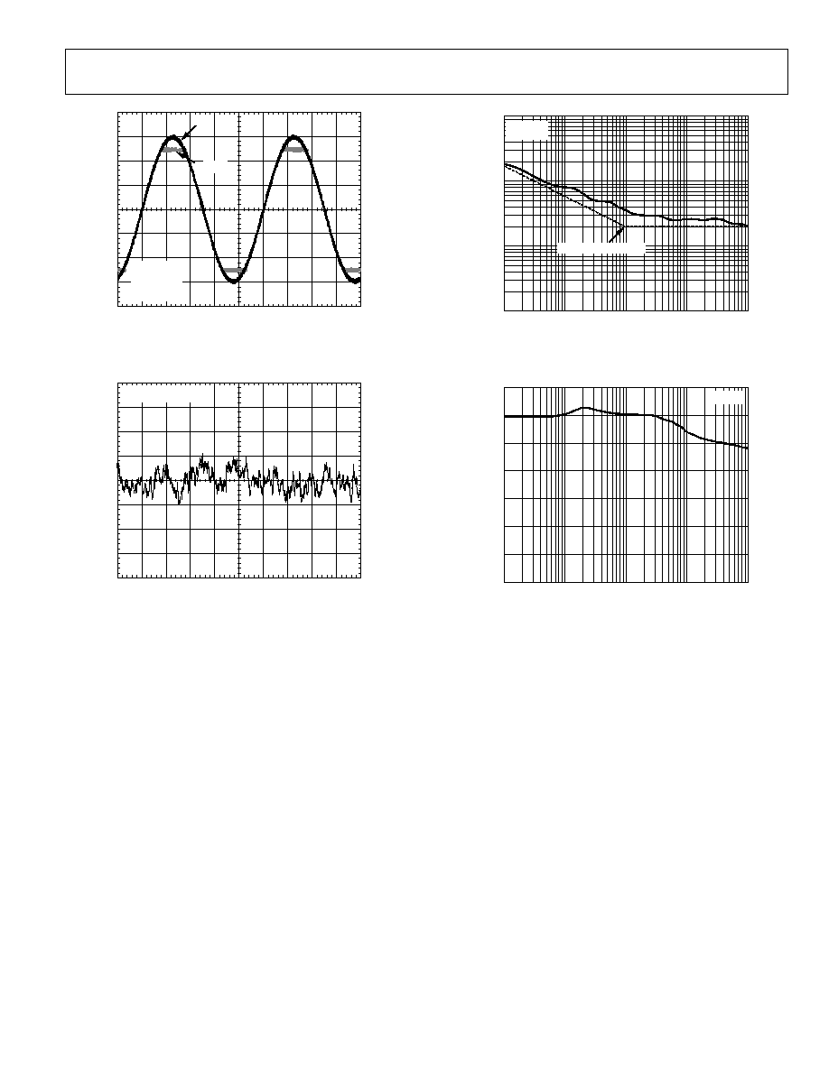
Figure 23. No Phase Reversal
05622-022
TIME (1s/DIV)
V
SY
= 5V AND 2.7V
VOLTA
GE N
OISE (
1
V/D
I
V)
Figure 24. 0.1 Hz to 10 Hz Input Voltage Noise
1000
1
1
10000
05622-023
FREQUENCY (Hz)
IN
PU
T VOLTA
GE N
OISE (
n
V/
Hz)
10
100
1000
10
100
V
SY
= 5V
T
A
= 25∫C
1/F CORNER @ 100Hz
Figure 25. Voltage Noise Density
140
0
100
1M
05622-024
FREQUENCY (Hz)
CHANNEL SEPARATION (dB)
20
40
60
80
100
120
1k
10k
100k
V
SY
= 5V
Figure 26. Channel Separation
AD8617/AD8619
Rev. A | Page 10 of 16
V
S
= 1.8 V or ±0.9 V, unless otherwise noted.
450
0
≠2000
1900
05622-025
INPUT OFFSET VOLTAGE (
V)
NUMBE
R OF AMP
LIFIE
RS
400
350
300
250
200
150
100
50
≠
1700
≠
1400
≠1100
≠800
≠500
≠200
100
400
700
1000
1300
1600
V
SY
= 1.8V
0V < V
CM
< 1.8V
T
A
= 25∞C
Figure 27. Input Offset Voltage Distribution
2000
≠2000
≠0.5
INPUT COMMON MODE VOLTAGE (V)
IN
PU
T OFFSET VOLTA
GE (
V)
2.2
1500
≠1500
≠1000
≠500
0
500
1000
≠0.2
0.1
0.4
0.7
1.0
1.3
1.6
1.9
V
SY
= 1.8V
T
A
= 25∞C
05622-026
Figure 28. Input Offset Voltage vs. Common-Mode Voltage
1000
0.01
0.001
10
05622-027
LOAD CURRENT (mA)
OU
TPU
T
SA
TU
R
A
TION
VOL
T
A
GE (
m
V)
0.01
0.1
1
0.1
1
10
100
V
SY
≠V
OH
SOURCE
V
SY
= 1.8V
T
A
= 25∫C
SINK
V
OL
Figure 29. Output Saturation Voltage vs. Load Current
80
0
≠40
125
05622-028
TEMPERATURE (∞C)
OUTP
UT S
A
TURATION V
O
LTAGE
(mV
)
60
40
20
≠25 ≠10
5
20
35
50
65
80
95
110
V
SY
= 1.8V
V
SY
≠V
OH
@ 1mA
V
OH
@ 1mA
Figure 30. Output Saturation Voltage vs. Temperature
(I
L
= 1 mA)
100
0
100
1M
05622-029
FREQUENCY (Hz)
CMRR (dB)
20
40
60
80
1k
10k
100k
V
SY
= 1.8V
T
A
= 25∞C
Figure 31. CMRR vs. Frequency
120
0
100
1M
05622-030
FREQUENCY (Hz)
P
S
RR (dB)
20
40
60
80
100
1k
10k
V
SY
= 1.8V
T
A
= 25∞C
Figure 32. PSRR vs. Frequency
AD8617/AD8619
Rev. A | Page 11 of 16
40
0
10
1k
05622-031
LOAD CAPACITANCE (pF)
SM
A
LL SIGN
A
L
OVER
SH
OOT (
%
)
10
20
30
100
+OS
≠OS
V
SY
= 1.8V
T
A
= 25∞C
Figure 33. Small Signal Overshoot vs. Load Capacitance
05622-032
TIME (20
s/DIV)
V
SY
= 1.8V
A
V
= 1
R
L
= 10k
C
L
= 200pF
VOLTA
GE (
500mV/D
IV)
Figure 34. Large Signal Transient Response
05622-033
TIME (1s/DIV)
V
SY
= 1.8V
VOLTAGE (1
V/D
I
V)
Figure 35. 0.1 Hz to 10 Hz Input Voltage Noise
1k
1
1
10k
05622-034
FREQUENCY (Hz)
IN
PU
T VOLTA
GE N
OISE (
n
V/
Hz)
10
100
1k
10
100
V
SY
= 1.8V
T
A
= 25∞C
1/F CORNER @ 100Hz
Figure 36. Voltage Noise Density

AD8617/AD8619
Rev. A | Page 12 of 16
OUTLINE DIMENSIONS
0.80
0.60
0.40
8∞
0∞
4
8
1
5
4.90
BSC
PIN 1
0.65 BSC
3.00
BSC
SEATING
PLANE
0.15
0.00
0.38
0.22
1.10 MAX
3.00
BSC
COPLANARITY
0.10
0.23
0.08
COMPLIANT TO JEDEC STANDARDS MO-187-AA
Figure 37. 8-Lead Mini Small Outline Package [MSOP]
(RM-8)
Dimensions shown in millimeters
CONTROLLING DIMENSIONS ARE IN MILLIMETERS; INCH DIMENSIONS
(IN PARENTHESES) ARE ROUNDED-OFF MILLIMETER EQUIVALENTS FOR
REFERENCE ONLY AND ARE NOT APPROPRIATE FOR USE IN DESIGN.
COMPLIANT TO JEDEC STANDARDS MS-012-AB
COPLANARITY
0.10
14
8
7
1
6.20 (0.2441)
5.80 (0.2283)
4.00 (0.1575)
3.80 (0.1496)
8.75 (0.3445)
8.55 (0.3366)
1.27 (0.0500)
BSC
SEATING
PLANE
0.25 (0.0098)
0.10 (0.0039)
0.51 (0.0201)
0.31 (0.0122)
1.75 (0.0689)
1.35 (0.0531)
8∞
0∞
0.50 (0.0197)
0.25 (0.0098)
1.27 (0.0500)
0.40 (0.0157)
0.25 (0.0098)
0.17 (0.0067)
◊
45∞
Figure 38. 14-Lead Standard Small Outline Package [SOIC_N]
Narrow Body
(R-14)
Dimensions shown in millimeters and ( inches)
0.25 (0.0098)
0.17 (0.0067)
1.27 (0.0500)
0.40 (0.0157)
0.50 (0.0196)
0.25 (0.0099)
◊
45∞
8∞
0∞
1.75 (0.0688)
1.35 (0.0532)
SEATING
PLANE
0.25 (0.0098)
0.10 (0.0040)
4
1
8
5
5.00 (0.1968)
4.80 (0.1890)
4.00 (0.1574)
3.80 (0.1497)
1.27 (0.0500)
BSC
6.20 (0.2440)
5.80 (0.2284)
0.51 (0.0201)
0.31 (0.0122)
COPLANARITY
0.10
CONTROLLING DIMENSIONS ARE IN MILLIMETERS; INCH DIMENSIONS
(IN PARENTHESES) ARE ROUNDED-OFF MILLIMETER EQUIVALENTS FOR
REFERENCE ONLY AND ARE NOT APPROPRIATE FOR USE IN DESIGN
COMPLIANT TO JEDEC STANDARDS MS-012-AA
Figure 39. 8-Lead Standard Small Outline Package [SOIC_N]
Narrow Body
(R-8)
Dimensions shown in millimeters and (inches)
4.50
4.40
4.30
14
8
7
1
6.40
BSC
PIN 1
5.10
5.00
4.90
0.65
BSC
SEATING
PLANE
0.15
0.05
0.30
0.19
1.20
MAX
1.05
1.00
0.80
0.20
0.09
8∞
0∞
0.75
0.60
0.45
COPLANARITY
0.10
COMPLIANT TO JEDEC STANDARDS MO-153-AB-1
Figure 40. 14-Lead Thin Shrink Small Outline Package [TSSOP]
(RU-14)
Dimensions shown in millimeters
AD8617/AD8619
Rev. A | Page 13 of 16
ORDERING GUIDE
Model
Temperature Range
Package Description
Package Option
Branding
AD8617ARMZ-R2
1
-40∞C to +125∞C
8-Lead MSOP
RM-8
A0T
AD8617ARMZ-REEL
1
-40∞C to +125∞C
8-Lead MSOP
RM-8
A0T
AD8617ARZ
1
-40∞C to +125∞C
8-Lead SOIC_N
R-8
AD8617ARZ-REEL
1
-40∞C to +125∞C
8-Lead SOIC_N
R-8
AD8617ARZ-REEL7
1
-40∞C to +125∞C
8-Lead SOIC_N
R-8
AD8619ARUZ
1
-40∞C to +125∞C
14-Lead TSSOP
RU-14
AD8619ARUZ-REEL
1
-40∞C to +125∞C
14-Lead TSSOP
RU-14
AD8619ARZ
1
-40∞C to +125∞C
14-Lead SOIC_N
R-14
AD8619ARZ-REEL
1
-40∞C to +125∞C
14-Lead SOIC_N
R-14
AD8619ARZ-REEL7
1
-40∞C to +125∞C
14-Lead SOIC_N
R-14
1
Z = Pb-free part.

AD8617/AD8619
Rev. A | Page 14 of 16
NOTES

AD8617/AD8619
Rev. A | Page 15 of 16
NOTES

AD8617/AD8619
Rev. A | Page 16 of 16
NOTES
© 2005 Analog Devices, Inc. All rights reserved. Trademarks and
registered trademarks are the property of their respective owners.
D05622-0-10/05(A)