Äîêóìåíòàöèÿ è îïèñàíèÿ www.docs.chipfind.ru
Ultra Precision, 36 V, 2.8 nV/Hz
Dual Rail-to-Rail Output Op Amp
AD8676
Rev. 0
Information furnished by Analog Devices is believed to be accurate and reliable. However, no
responsibility is assumed by Analog Devices for its use, nor for any infringements of patents or other
rights of third parties that may result from its use. Specifications subject to change without notice. No
license is granted by implication or otherwise under any patent or patent rights of Analog Devices.
Trademarks and registered trademarks are the property of their respective owners.
One Technology Way, P.O. Box 9106, Norwood, MA 02062-9106, U.S.A.
Tel: 781.329.4700
www.analog.com
Fax: 781.461.3113
©2006 Analog Devices, Inc. All rights reserved.
FEATURES
Very low voltage noise 2.8 nV/Hz @ 1 kHz
Rail-to-rail output swing
Low input bias current: 2 nA maximum
Very low offset voltage: 12 V typical
Low input offset drift: 0.6 V/°C maximum
Very high gain: 120 dB
Wide bandwidth: 10 MHz typical
±5 V to ±18 V operation
APPLICATIONS
Precision instrumentation
PLL filters
Laser diode control loops
Strain gage amplifiers
Medical instrumentation
Thermocouple amplifiers
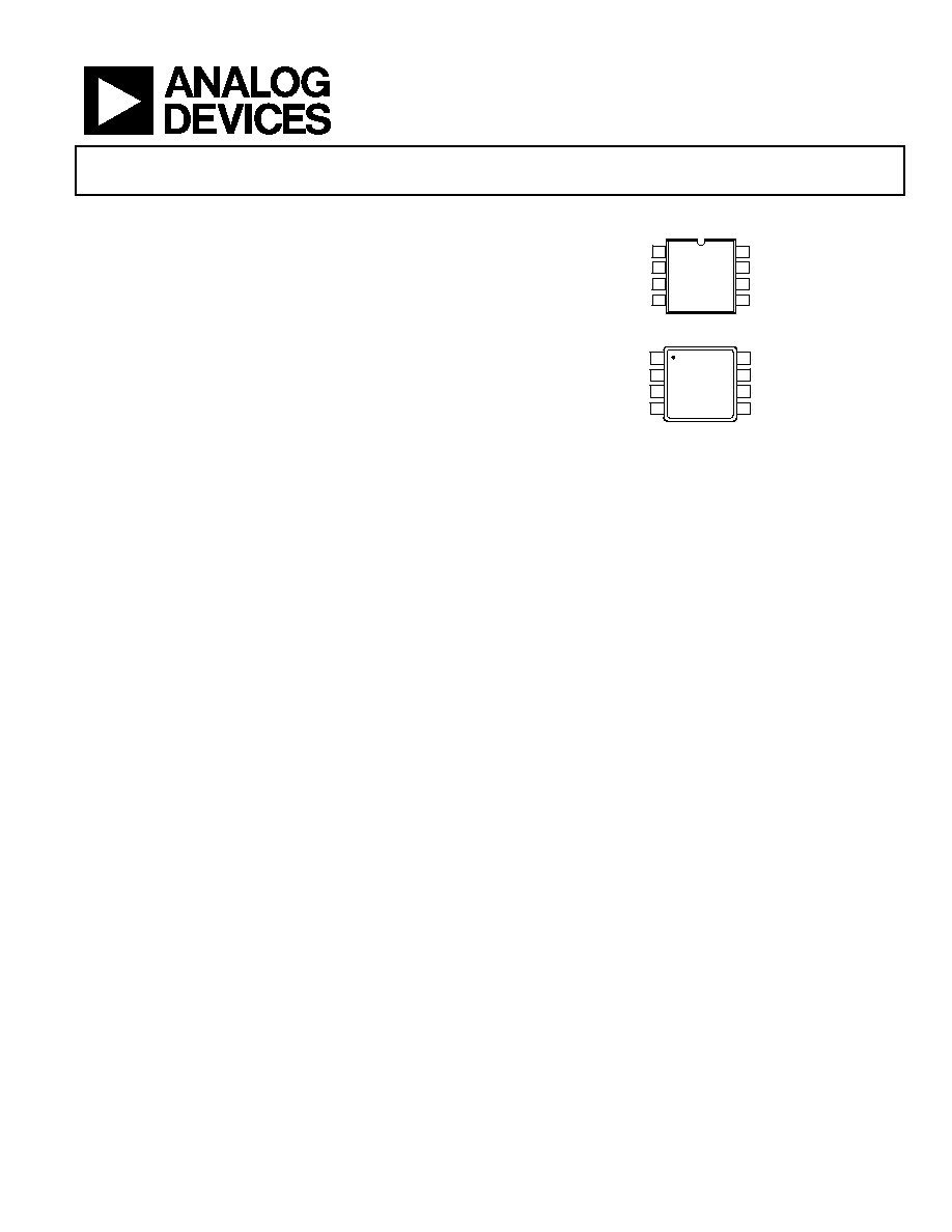
PIN CONFIGURATIONS
OUT A
1
IN A
2
+IN A
3
V
4
V+
8
OUT B
7
IN B
6
+IN B
5
AD8676
TOP VIEW
(Not to Scale)
064
87-
00
1
Figure 1. 8-Lead SOIC_N (R-8)
OUT A
1
IN A
2
+IN A
3
V
4
V+
8
OUT B
7
IN B
6
+IN B
5
AD8676
TOP VIEW
(Not to Scale)
0648
7-
00
2
Figure 2. 8-Lead MSOP (RM-8)
GENERAL DESCRIPTION
The AD8676 precision operational amplifier offers ultralow
offset, drift, and voltage noise combined with very low input
bias currents over the full operating temperature range. The
AD8676 is a precision, wide bandwidth op amp featuring rail-to-
rail output swings and very low noise. Operation is fully
specified from ±5 V to ±15 V.
The AD8676 features a rail-to-rail output like that of the OP184,
but with wide bandwidth and even lower voltage noise, com-
bined with the precision and low power consumption like that
of the industry-standard OP07 amplifier. Unlike other low
noise, rail-to-rail op amps, the AD8676 has very low input bias
current and low input current noise.
With typical offset voltage of only 12 V, offset drift of 0.2 V/°C,
and noise of only 0.10 V p-p (0.1 Hz to 10 Hz), the AD8676 is
perfectly suited for applications where large error sources
cannot be tolerated. Precision instrumentation, PLL and other
precision filter circuits, position and pressure sensors, medical
instrumentation, and strain gage amplifiers benefit greatly from
the very low noise, low input bias current, and wide bandwidth.
Many systems can take advantage of the low noise, dc precision,
and rail-to-rail output swing provided by the AD8676 to maxi-
mize SNR and dynamic range.
The smaller packages and low power consumption afforded by
the AD8676 allow maximum channel density or minimum
board size for space-critical equipment.
The AD8676 is specified for the extended industrial temperature
range (-40°C to +125°C). The AD8676 is available in the 8-lead
MSOP, and the popular 8-lead, narrow SOIC; both of which are
lead-free packages. MSOP packaged devices are only available
in tape and reel format.
For the single version of this ultraprecision rail-to-rail op amp,
see the AD8675 data sheet.

AD8676
Rev. 0 | Page 2 of 12
TABLE OF CONTENTS
Features .............................................................................................. 1
Applications....................................................................................... 1
Pin Configurations ........................................................................... 1
General Description ......................................................................... 1
Revision History ............................................................................... 2
Specifications..................................................................................... 3
Electrical Specifications............................................................... 3
Absolute Maximum Ratings ............................................................5
Thermal Resistance .......................................................................5
Power Sequencing .........................................................................5
ESD Caution...................................................................................5
Typical Performance Characteristics ..............................................6
Outline Dimensions ....................................................................... 10
Ordering Guide .......................................................................... 10
REVISION HISTORY
10/06--Revision 0: Initial Version

AD8676
Rev. 0 | Page 3 of 12
SPECIFICATIONS
ELECTRICAL SPECIFICATIONS
V
S
= ±5.0 V, V
CM
= 0 V, V
O
= 0 V, T
A
= +25°C, unless otherwise specified.
Table 1.
Parameter Symbol
Conditions
Min
Typ
Max
Unit
INPUT CHARACTERISTICS
Offset Voltage
V
OS
B Grade (SOIC)
12
50
V
B Grade (MSOP)
60
V
A Grade (SOIC, MSOP)
100
V
Offset Voltage
V
OS
-40°C T
A
+125°C
B Grade (SOIC, MSOP)
15
160
V
A Grade (SOIC, MSOP)
250
V
Input Bias Current
I
B
-2
+0.5
+2
nA
-40°C
T
A
+125°C
-5.5
+1
+5.5
nA
Input Offset Current
I
OS
-1
+0.1
+1
nA
-40°C
T
A
+125°C
-2.8
+0.1
+2.8
nA
Input Voltage Range
-3.5
+3.5
V
Common-Mode Rejection Ratio
CMRR
V
CM
= -3.0 V to +3.0 V
105
130
dB
-40°C
T
A
+125°C
105
130
dB
Open-Loop Gain
A
VO
R
L
= 2 k to ground,
1000
2000
V/mV
V
O
= -3.5 V to +3.5 V
-40°C
T
A
+125°C
700
1250
V/mV
Offset Voltage Drift
V
OS
/T -40°C
T
A
+125°C
0.2
0.6
V/°C
OUTPUT CHARACTERISTICS
Output Voltage High
V
OH
R
L
= 2 k to ground
+4.84
+4.86
V
-40°C
T
A
+125°C
+4.78
+4.82
V
Output Voltage Low
V
OL
R
L
= 2 k to ground
-4.95
-4.86
V
-40°C
T
A
+125°C
-4.93
-4.82
V
Short-Circuit Limit
I
SC
+40
mA
Output Current
I
O
±20
mA
POWER SUPPLY
Power Supply Rejection Ratio
PSRR
V
S
= ±5.0 V to ±15.0 V
106
120
dB
-40°C
T
A
+125°C
106
120
dB
Supply Current/Amplifier
I
SY
V
O
= 0 V
2.3
2.7
mA
-40°C
T
A
+125°C
2.7
3.4
mA
DYNAMIC PERFORMANCE
Slew Rate
SR
R
L
= 2 k
2.5
V/s
Gain Bandwidth Product
GBP
10
MHz
NOISE PERFORMANCE
Voltage Noise
e
n p-p
0.1 Hz to 10 Hz
0.1
V p-p
Voltage Noise Density
e
n
f = 1 kHz
2.8
nV/Hz
Current Noise Density
i
n
f = 10 Hz
0.3
pA/Hz

AD8676
Rev. 0 | Page 4 of 12
V
S
= ±15 V, V
CM
= 0 V, V
O
= 0 V, T
A
= +25°C, unless otherwise specified.
Table 2.
Parameter Symbol
Conditions
Min
Typ
Max
Unit
INPUT CHARACTERISTICS
Offset Voltage
V
OS
B Grade (SOIC)
12
50
V
B Grade (MSOP)
60
V
A Grade (SOIC, MSOP)
100
V
Offset Voltage
V
OS
-40°C T
A
+125°C
B Grade (SOIC, MSOP)
15
160
V
A Grade (SOIC, MSOP)
250
V
Input Bias Current
I
B
-2
-0.5
+2
nA
-40°C
T
A
+125°C
-4.5
-1
+4.5
nA
Input Offset Current
I
OS
-1
-0.1
+1
nA
-40°C
T
A
+125°C
-2.8
-0.1
+2.8
nA
Input Voltage Range
-13.5
+13.5
V
Common-Mode Rejection Ratio
CMRR
V
CM
= -12.5 V to +12.5 V
111
130
dB
-40°C
T
A
+125°C
107
130
dB
Open-Loop Gain
A
VO
R
L
= 2 k to ground,
1500
4000
V/mV
V
O
= -13.5 V to +13.5 V
-40°C
T
A
+125°C
700
1700
V/mV
Offset Voltage Drift
V
OS
/T -40°C
T
A
+125°C
0.2
0.6
V/°C
OUTPUT CHARACTERISTICS
Output Voltage High
V
OH
R
L
= 2 k to ground
+14.65
+14.7
V
-40°C
T
A
+125°C
+14.49
+14.59
V
Output Voltage Low
V
OL
R
L
= 2 k to ground
-14.88
-14.75
V
-40°C
T
A
+125°C
-14.83
-14.69
V
Short-Circuit Limit
I
SC
+40
mA
Output Current
I
O
±20
mA
POWER SUPPLY
Power Supply Rejection Ratio
PSRR
V
S
= ±5.0 V to ±15.0 V
106
120
dB
-40°C
T
A
+125°C
106
120
dB
Supply Current/Amplifier
I
SY
V
O
= 0 V
2.5
2.9
mA
-40°C
T
A
+125°C
2.9
3.8
mA
DYNAMIC PERFORMANCE
Slew Rate
SR
R
L
=10 k
2.5
V/s
Gain Bandwidth Product
GBP
10
MHz
NOISE PERFORMANCE
Voltage Noise
e
n p-p
0.1 Hz to 10 Hz
0.1
V p-p
Voltage Noise Density
e
n
f = 1 kHz
2.8
nV/Hz
Current Noise Density
i
n
f = 10 Hz
0.3
pA/Hz
AD8676
Rev. 0 | Page 5 of 12
ABSOLUTE MAXIMUM RATINGS
Table 3.
Parameter Rating
Supply Voltage
±18 V
Input Voltage
±V Supply - 1.5 V
Differential Input Voltage
±0.7 V
Output Short-Circuit Duration to GND
Indefinite
Storage Temperature Range
RM, R Packages
-65°C to +150°C
Operating Temperature Range
-40°C to +125°C
Junction Temperature Range
RM, R Packages
-65°C to +150°C
Lead Temperature Range (Soldering, 10 sec)
300°C
Stresses above those listed under Absolute Maximum Ratings
may cause permanent damage to the device. This is a stress
rating only; functional operation of the device at these or any
other conditions above those indicated in the operational
section of this specification is not implied. Exposure to absolute
maximum rating conditions for extended periods may affect
device reliability.
THERMAL RESISTANCE
Table 4. Thermal Resistance
Package Type
JA
JC
Unit
8-Lead MSOP (RM)
210
45
°C/W
8-Lead SOIC_N (R)
158
43
°C/W
POWER SEQUENCING
The op amp supplies must be established simultaneously with,
or before, any input signals are applied.
If this is not possible, the input current must be limited to 10 mA.
ESD CAUTION
AD8676
Rev. 0 | Page 6 of 12
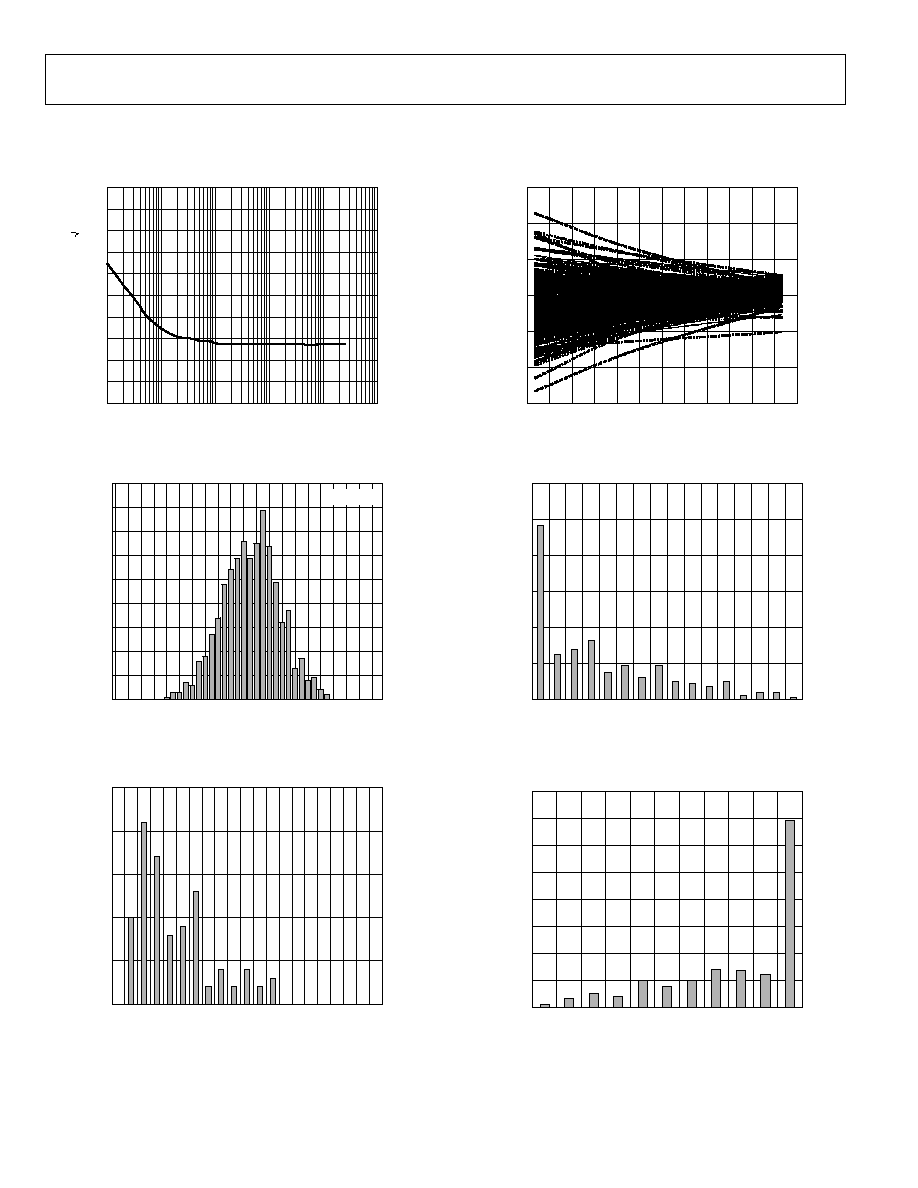
TYPICAL PERFORMANCE CHARACTERISTICS
±15 V and ±5 V, T
A
= 25°C, unless otherwise specified.
10
9
8
7
6
5
4
3
2
1
0
1
10
100
1k
10k
100k
FREQUENCY (Hz)
VO
L
T
A
G
E
N
O
I
S
E
D
EN
SI
T
Y
(
n
V/
H
z
)
06
48
7-
00
3
Figure 3. Voltage Noise Density vs. Frequency
90
0
100 80
60
40
20
0
20
40
60
80
100
V
OS
(µV)
N
U
MB
E
R
OF
A
M
P
L
IF
IE
R
S
80
70
60
50
40
30
20
10
06
48
7-
0
04
T
A
= 25°C
Figure 4. Input Offset Voltage Distribution
25
20
15
10
5
0
0
0.
05
0.
10
0.
15
0.
20
0.
25
0.
30
0.
35
0.
40
0.
45
0.
50
0.
55
0.
60
1.
00
0.
65
0.
70
0.
75
0.
80
0.
85
0.
90
0.
95
T
C
V
OS
(µV/°C)
NUM
BE
R O
F
AM
P
L
I
F
I
E
RS
06
48
7-
0
05
Figure 5. T
C
V
OS
Distribution
150
150
45
135
TEMPERATURE (°C)
V
OS
(µ
V
)
100
50
0
50
100
30 15
0
15
30
45
60
75
90
105 120
06
48
7-
00
6
Figure 6. Offset Voltage vs. Temperature
120
0
0.65
06
48
7-
0
07
I
B
(nA)
N
U
MB
E
R
OF
A
M
P
L
IF
IE
R
S
100
80
60
40
20
0.55
0.45
0.35
0.25
0.15
0.05
0.05
Figure 7. Input Bias Current, V
SY
= ±15 V
160
0
0.65
06
48
7-
0
08
I
B
(nA)
N
U
MB
E
R
OF
A
M
P
L
IF
IE
R
S
140
120
100
80
60
40
20
0.60 0.55 0.50 0.45 0.40 0.35 0.30 0.25 0.20 0.15
Figure 8. Input Bias Current, V
SY
= ±5 V
AD8676
Rev. 0 | Page 7 of 12
5
4
3
2
1
0
1
2
3
4
5
40
20
0
20
40
60
80
100
120
TEMPERATURE (°C)
I
B
(nA
)
V
SY
= ±5V
V
SY
= ±15V
06
48
7-
00
9
Figure 9. Input Bias Current vs. Temperature
3.0
2.5
2.0
1.5
1.0
0.5
0
5
10
15
20
25
30
35
SUPPLY VOLTAGE (V)
S
UP
P
L
Y
CURR
E
NT
(
m
A)
06
48
7-
01
0
Figure 10. Supply Current vs. Total Supply Voltage
3.5
3.0
2.5
2.0
1.5
1.0
0.5
0
40
20
0
20
40
60
80
100
120
TEMPERATURE (°C)
S
UP
P
L
Y
CURR
E
NT
(
m
A)
V
S
= ±15V
V
S
= ±5V
06
48
7-
01
1
Figure 11. Supply Current vs. Temperature
100
120
100
80
40
60
20
40
20
0
80
100
60
120
10k
1k
100k
10M
1M
100M
FREQUENCY (Hz)
GA
IN
(
d
B
)
R
L
= 2k
C
L
= 35pF
M
= 55.2
GAIN
PHASE
180
120
60
60
0
120
180
P
HAS
E
M
A
RG
I
N
(
D
eg
r
ees)
06
48
7-
01
2
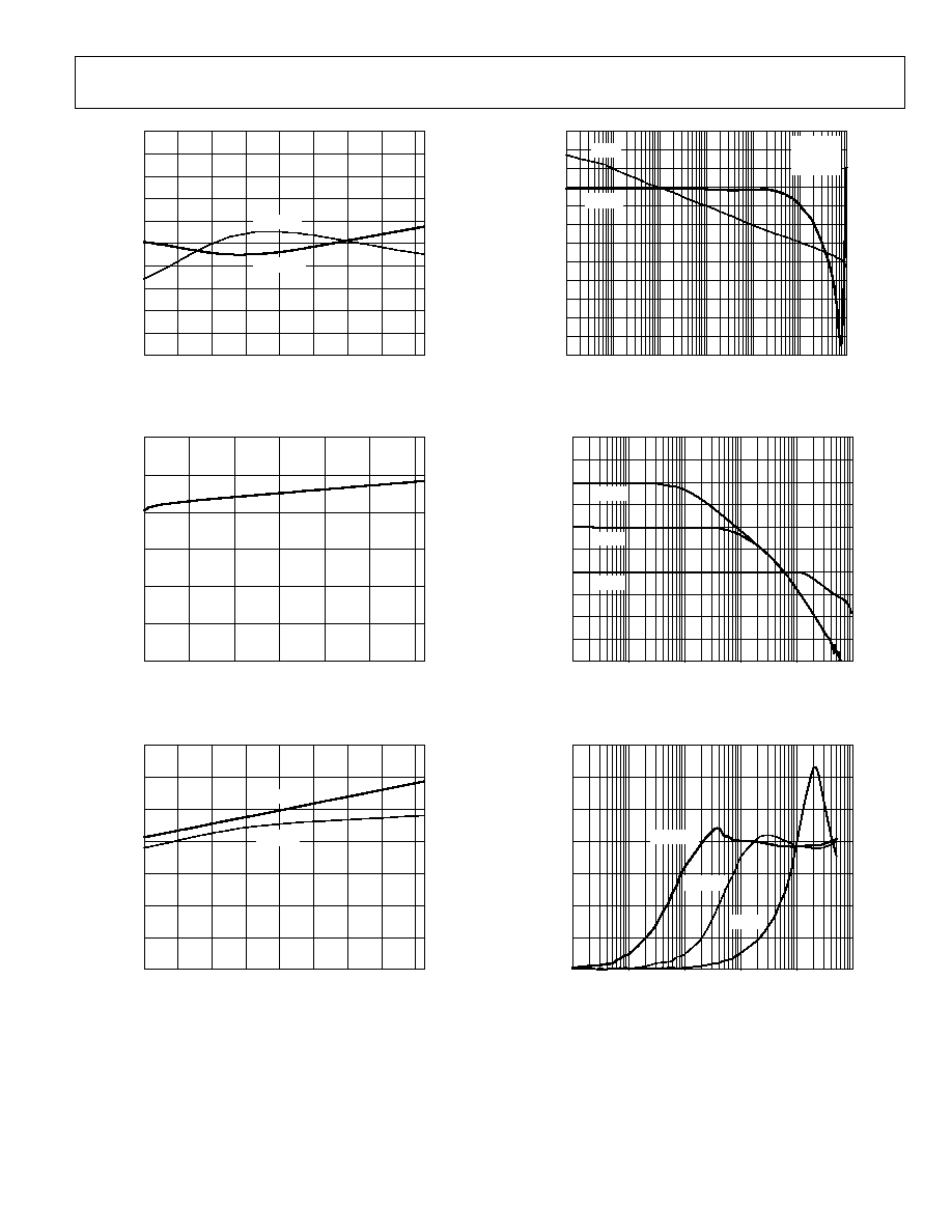
Figure 12. Gain and Phase vs. Frequency
60
50
40
30
20
10
0
10
20
30
40
1k
10k
100k
G = 1
G = 10
G = 100
1M
10M
100M
FREQUENCY (Hz)
C
L
OS
E
D
-
L
OO
P
GA
IN
(
d
B
)
06
48
7-
01
3
Figure 13. Closed-Loop Gain vs. Frequency
70
60
50
40
30
20
10
0
1k
10k
100k
1M
10M
100M
FREQUENCY (Hz)
Z
OU
T
(
)
A
VO
= 100
A
VO
= 10
A
VO
= 1
06
48
7-
01
4
Figure 14. Z
OUT
vs. Frequency
AD8676
Rev. 0 | Page 8 of 12
15
10
5
0
5
10
15
TIME (10µs/DIV)
VO
L
T
A
G
E
(
V)
V
IN
= ±10V
R
L
= 2k
A
V
= +1
06
48
7-
01
5
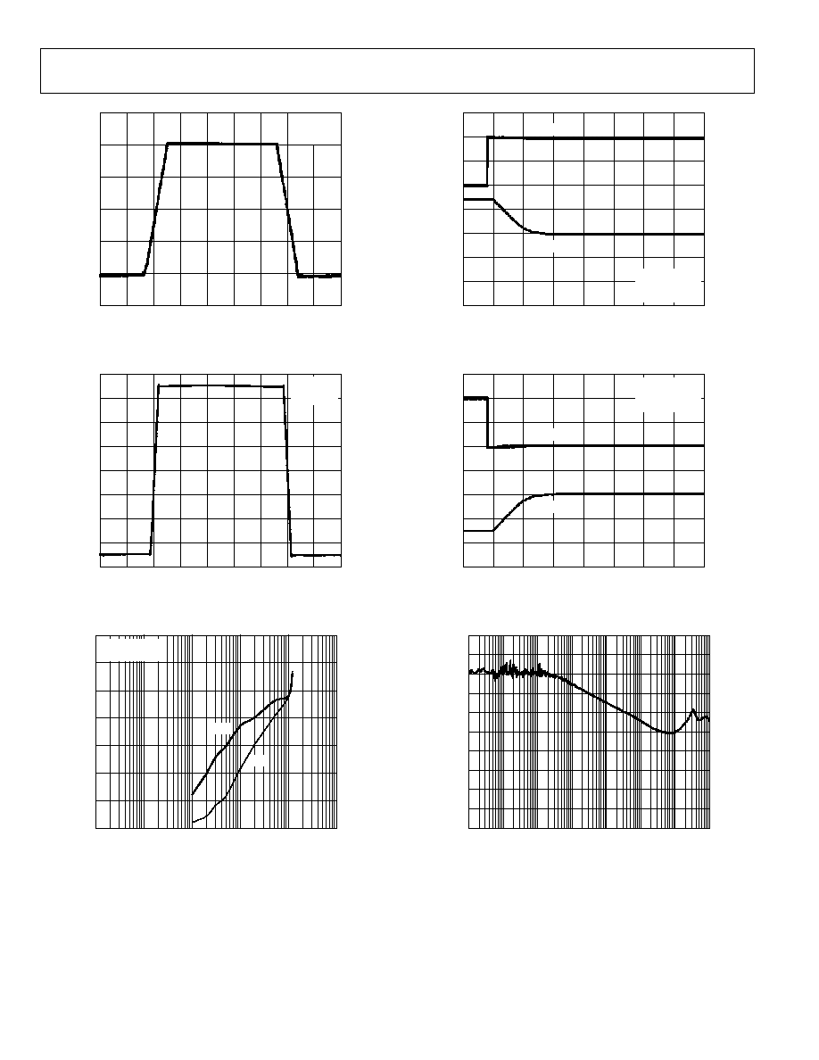
Figure 15. Large Signal Transient Response, V
SY
= ±15 V
4
3
2
1
0
1
3
2
4
TIME (10µs/DIV)
VO
L
T
A
G
E
(
V)
V
IN
= ±3.5V
R
L
= 2k
A
V
= +1
06
48
7-
01
6
Figure 16. Large Signal Transient Response, V
SY
= ±5 V
70
60
50
40
30
20
10
0
1
10
100
1k
10k
100k
CAPACITANCE (pF)
O
VER
SH
O
O
T
(
%
)
A
V
= +1
V
IN
= 100mV p-p
+OS
OS
06
48
7-
01
7
Figure 17. Small Signal Overshoot vs. Load Capacitance
0.1
0
0.1
0.2
0.3
0.4
0.5
0.6
0.7
4
1
6
11
16
21
26
31
36
TIME (µs)
I
N
PU
T
VO
L
T
A
G
E (
V)
50
40
30
20
10
0
10
30
20
OU
TP
U
T
V
O
LT
A
G
E
(
V
)
V
IN
= 200mV p-p
A
VO
= 100
R
L
= 10k
V
IN
V
OUT
06
48
7-
01
8
Figure 18. Positive Overvoltage Recovery
0.3
0.2
0.1
0
0.1
0.2
0.3
0.4
0.5
4
1
6
11
16
21
26
31
36
TIME (µs)
I
N
PU
T
VO
L
T
A
G
E (
V)
50
40
30
20
10
0
10
20
30
OU
TP
U
T
V
O
LT
A
G
E
(
V
)
V
IN
= 200mV p-p
A
VO
= 100
R
L
= 10k
V
IN
V
OUT
06
48
7-
01
9
Figure 19. Negative Overvoltage Recovery
180
160
140
120
100
80
60
40
20
0
20
10
100
10k
1k
100k
10M
1M
100M
FREQUENCY (Hz)
CM
R
R (
d
B)
06
48
7-
02
0
Figure 20. CMRR vs. Frequency
AD8676
Rev. 0 | Page 9 of 12
160
140
120
100
60
80
20
40
0
20
10
100
10k
1k
100k
10M
1M
100M
FREQUENCY (Hz)
P
O
W
E
R
S
U
P
P
L
Y
R
E
JE
CT
I
O
N
RAT
I
O
(
d
B
)
PSRR
+PSRR
06
48
7-
02
1
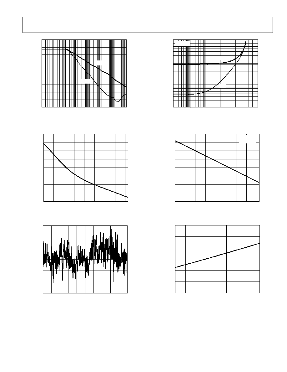
Figure 21. Power Supply Rejection Ratio vs. Frequency
148
147
146
145
144
143
142
141
140
40
20
0
20
40
60
80
100
120
TEMPERATURE (°C)
P
O
W
E
R
S
U
P
P
L
Y
R
E
JE
CT
I
O
N
RAT
I
O
(
d
B
)
06
48
7-
02
2
Figure 22. Power Supply Rejection Ratio vs. Temperature
0.06
0.04
0.02
0
0.02
0.04
0.06
0
1
2
4
3
7
6
5
8
9
TIME (s)
NO
I
S
E
(
µ
V
)
10
0
64
87
-
02
3
Figure 23. Voltage Noise (0.1 Hz to 10 Hz)
1000
100
10
1
0.001
0.01
0.1
1
10
100
LOAD CURRENT (mA)
V
S
V
OU
T
(m
V)
T
A
= 25°C
SOURCE
SINK
06
48
7-
02
4
Figure 24. Output Saturation Voltage vs. Output Load Current
14.86
14.84
14.82
14.80
14.78
14.76
14.74
14.72
14.70
40
20
0
20
40
60
80
100
120
TEMPERATURE (°C)
+S
W
I
N
G
(V
)
V
OH
V
SY
=
±15V
R
L
= 2k
06
48
7-
02
5
Figure 25. +Swing vs. Temperature, V
OH
14.70
14.75
14.80
14.85
14.90
14.95
15.00
40
20
0
20
40
60
80
100
120
TEMPERATURE (°C)
SW
I
N
G
(
V)
V
SY
=
±15V
R
L
= 2k
V
OL
06
48
7-
02
6
Figure 26. -Swing vs. Temperature, V
OL
AD8676
Rev. 0 | Page 10 of 12
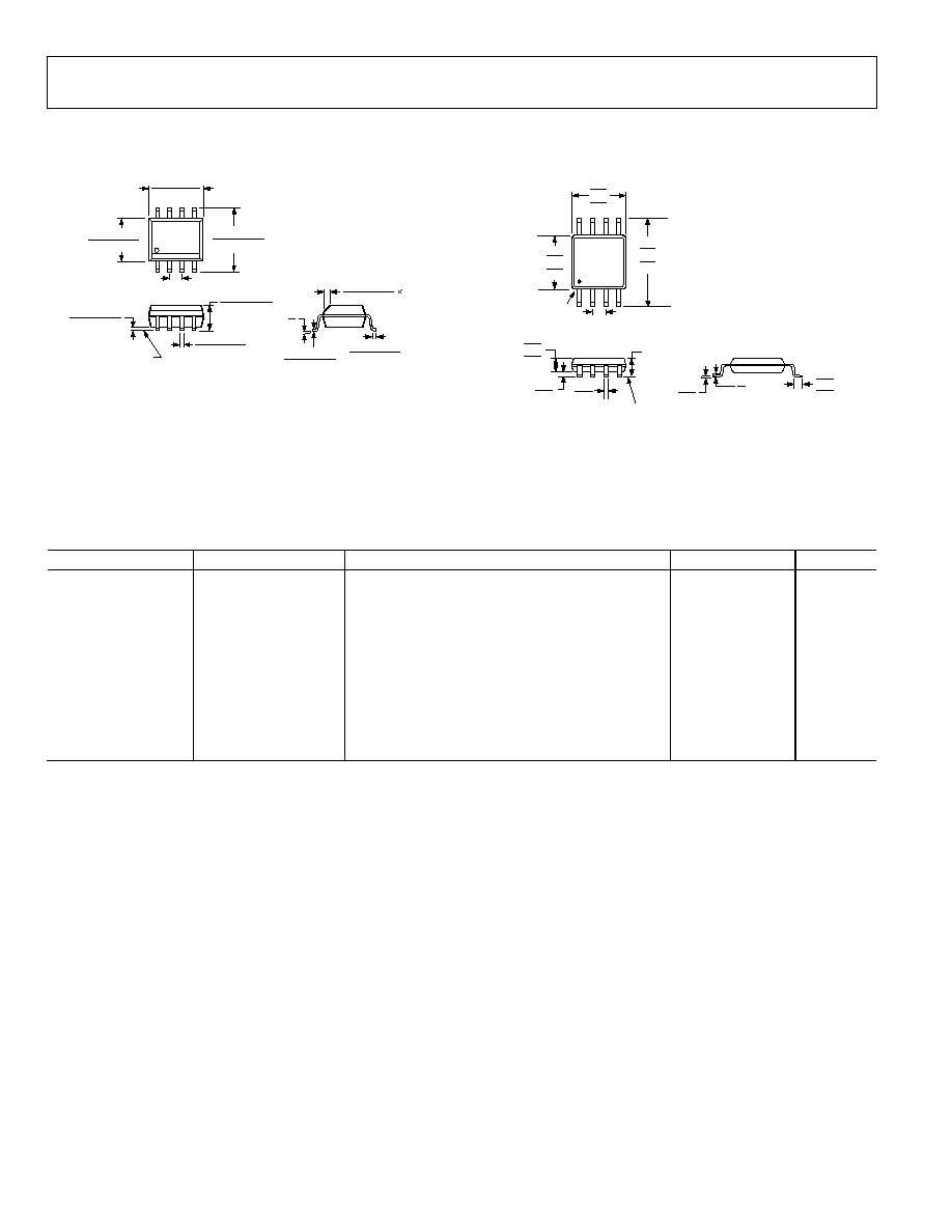
OUTLINE DIMENSIONS
CONTROLLING DIMENSIONS ARE IN MILLIMETERS; INCH DIMENSIONS
(IN PARENTHESES) ARE ROUNDED-OFF MILLIMETER EQUIVALENTS FOR
REFERENCE ONLY AND ARE NOT APPROPRIATE FOR USE IN DESIGN.
COMPLIANT TO JEDEC STANDARDS MS-012-A A
0
605
06-
A
0.25 (0.0098)
0.17 (0.0067)
1.27 (0.0500)
0.40 (0.0157)
0.50 (0.0196)
0.25 (0.0099)
45°
8°
0°
1.75 (0.0688)
1.35 (0.0532)
SEATING
PLANE
0.25 (0.0098)
0.10 (0.0040)
4
1
8
5
5.00 (0.1968)
4.80 (0.1890)
4.00 (0.1574)
3.80 (0.1497)
1.27 (0.0500)
BSC
6.20 (0.2440)
5.80 (0.2284)
0.51 (0.0201)
0.31 (0.0122)
COPLANARITY
0.10
Figure 27. 8-Lead Standard Small Outline Package [SOIC_N]
Narrow Body (R-8)
Dimensions shown in millimeters and (inches)
COMPLIANT TO JEDEC STANDARDS MO-187-AA
0.80
0.60
0.40
8°
0°
4
8
1
5
PIN 1
0.65 BSC
SEATING
PLANE
0.38
0.22
1.10 MAX
3.20
3.00
2.80
COPLANARITY
0.10
0.23
0.08
3.20
3.00
2.80
5.15
4.90
4.65
0.15
0.00
0.95
0.85
0.75
Figure 28. 8-Lead Mini Small Outline Package [MSOP]
(RM-8)
Dimensions shown in millimeters
ORDERING GUIDE
Model
Temperature Range
Package Description
Package Option
Branding
AD8676ARMZ-R2
1
-40°C to +125°C
8-Lead Mini Small Outline Package [MSOP]
RM-8
A13
AD8676ARMZ-REEL
1
-40°C to +125°C
8-Lead Mini Small Outline Package [MSOP]
RM-8
A13
AD8676ARZ
1
-40°C to +125°C
8-Lead Standard Small Outline Package [SOIC_N]
R-8
AD8676ARZ-REEL
1
-40°C to +125°C
8-Lead Standard Small Outline Package [SOIC_N]
R-8
AD8676ARZ-REEL7
1
-40°C to +125°C
8-Lead Standard Small Outline Package [SOIC_N]
R-8
AD8676BRMZ-R2
1
-40°C to +125°C
8-Lead Mini Small Outline Package [MSOP]
RM-8
A1L
AD8676BRMZ-REEL
1
-40°C to +125°C
8-Lead Mini Small Outline Package [MSOP]
RM-8
A1L
AD8676BRZ
1
-40°C to +125°C
8-Lead Standard Small Outline Package [SOIC_N]
R-8
AD8676BRZ-REEL
1
-40°C to +125°C
8-Lead Standard Small Outline Package [SOIC_N]
R-8
AD8676BRZ-REEL7
1
-40°C to +125°C
8-Lead Standard Small Outline Package [SOIC_N]
R-8
1
Z = Pb-free part.

AD8676
Rev. 0 | Page 11 of 12
NOTES

AD8676
Rev. 0 | Page 12 of 12
NOTES
©2006 Analog Devices, Inc. All rights reserved. Trademarks and
registered trademarks are the property of their respective owners.
D05564-0-10/06(0)
Document Outline
- þÿ
- þÿ
- þÿ
- þÿ
- þÿ
- þÿ
- þÿ
- þÿ
- þÿ
- þÿ
- þÿ
- þÿ
- þÿ