 | ÐлекÑÑоннÑй компоненÑ: AD8682ARZ | СкаÑаÑÑ:  PDF PDF  ZIP ZIP |
Äîêóìåíòàöèÿ è îïèñàíèÿ www.docs.chipfind.ru
Dual/Quad Low Power, High Speed
JFET Operational Amplifiers
AD8682/AD8684
Rev. 0
Information furnished by Analog Devices is believed to be accurate and reliable. However, no
responsibility is assumed by Analog Devices for its use, nor for any infringements of patents or other
rights of third parties that may result from its use. Specifications subject to change without notice. No
license is granted by implication or otherwise under any patent or patent rights of Analog Devices.
Trademarks and registered trademarks are the property of their respective owners.
One Technology Way, P.O. Box 9106, Norwood, MA 02062-9106, U.S.A.
Tel: 781.329.4700
www.analog.com
Fax: 781.461.3113
©2006 Analog Devices, Inc. All rights reserved.
FEATURES
Low supply current: 250 A/amp maximum
High slew rate: 9 V/s
Bandwidth: 3.5 MHz typical
Low offset voltage: 1 mV maximum @ 25°C
Low input bias current: 20 pA maximum @ 25°C
CMRR: 90 dB typical
Fast settling time
Unity gain stable
APPLICATIONS
Portable telecommunication
Low power industrial and instrumentation
Loop filters
Active and precision filters
Integrators
Strain gauge amplifiers
Portable medical instrumentation
Supply current monitoring
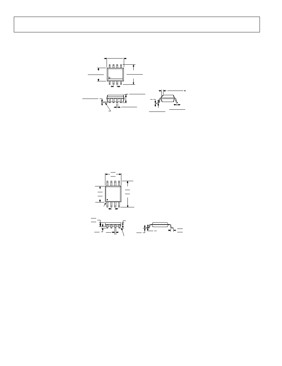
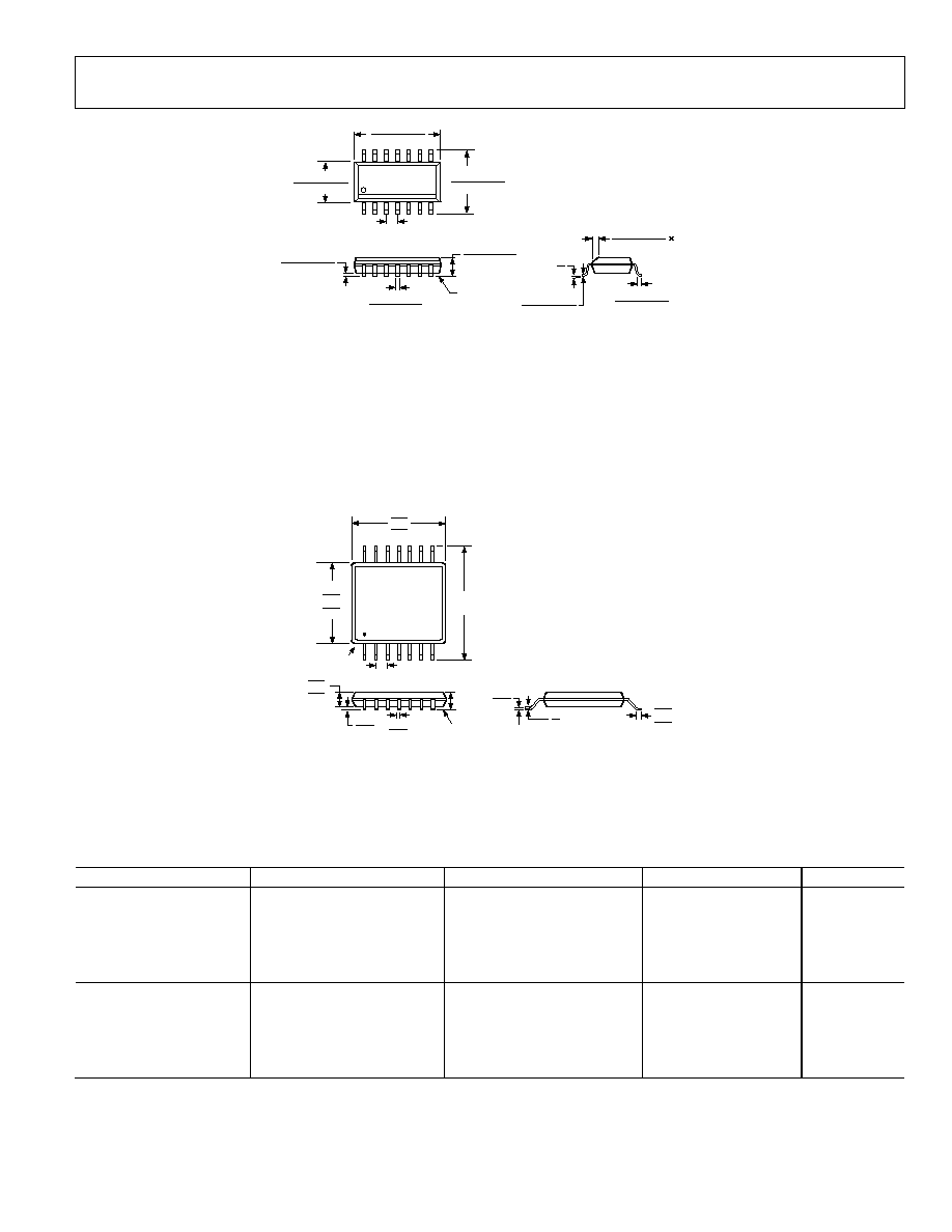
PIN CONFIGURATIONS
OUT A
1
IN A
2
+IN A
3
V
4
V+
8
OUT B
7
IN B
6
+IN B
5
AD8682
TOP VIEW
(Not to Scale)
0
62
78
-
0
01
Figure 1. 8-Lead SOIC_N and 8-Lead MSOP
OUT A
1
IN A
2
+IN A
3
V+
4
OUT D
14
IN D
13
+IN D
12
V
11
+IN B
5
+IN C
10
IN B
6
IN C
9
OUT B
7
OUT C
8
AD8684
TOP VIEW
(Not to Scale)
06
27
8-
0
02
Figure 2. 14-Lead SOIC_N and 14-Lead TSSOP
GENERAL DESCRIPTION
The AD8682 and AD8684 are dual and quad low power, precision
(1 mV) JFET amplifiers featuring excellent speed at low supply
currents. The slew rate is typically 9 V/s with a supply current
under 250 A per amplifier. These unity-gain stable amplifiers
have a typical gain bandwidth of 3.5 MHz. The JFET input stage
ensures bias current is typically a few picoamps and below 125 pA
maximum over the full temperature operating range.
The devices are ideal for portable, low power applications,
especially with high source impedance. The devices are unity gain
stable and can drive higher capacity loads (G = 1, noninverting),
as an example of their excellent dynamic response over a wide
range of conditions, delivering dc precision performance at low
quiescent currents.

AD8682/AD8684
Rev. 0 | Page 2 of 16
TABLE OF CONTENTS
Features .............................................................................................. 1
Applications....................................................................................... 1
Pin Configurations ........................................................................... 1
General Description ......................................................................... 1
Revision History ............................................................................... 2
Specifications..................................................................................... 3
Electrical Characteristics............................................................. 3
Absolute Maximum Ratings............................................................ 4
Thermal Resistance ...................................................................... 4
ESD Caution...................................................................................4
Typical Performance Characteristic................................................5
Applications Information .............................................................. 10
High-Side Signal Conditioning ................................................ 10
Phase Inversion........................................................................... 10
Active Filters ............................................................................... 10
Programmable State Variable Filter ......................................... 11
Outline Dimensions ....................................................................... 12
Ordering Guide .......................................................................... 13
REVISION HISTORY
10/06--Revision 0: Initial Version

AD8682/AD8684
Rev. 0 | Page 3 of 16
SPECIFICATIONS
ELECTRICAL CHARACTERISTICS
V
S
= ±15.0 V, T
A
= 25°C, V
CM
= 0 V, unless otherwise noted.
Table 1.
Parameter Symbol
Conditions
Min
Typ
Max
Unit
INPUT
CHARACTERISTICS
Offset Voltage
V
OS
0.35
1 mV
AD8682:
+25°C
T
A
+85°C
2.5
mV
AD8684:
+25°C
T
A
+85°C
3.5
mV
AD8682:
-40°C
T
A
+25°C
3
mV
AD8684:
-40°C
T
A
+25°C
4
mV
Input Bias Current
I
B
6
20
pA
-40°C
T
A
+85°C
125
pA
Input Offset Current
I
OS
20
pA
-40°C
T
A
+85°C
100
pA
Input Voltage Range
-11
+15
V
Common-Mode Rejection Ratio
CMRR
-11 V V
CM
+15 V, -40°C T
A
+85°C 70 90
dB
Large Signal Voltage Gain
A
VO
R
L
= 10 k
20
V/mV
R
L
= 10 k, -40°C T
A
+85°C
15
V/mV
Offset Voltage Drift
V
OS
/T
10
V/°C
Bias Current Drift
I
B
/T
8
pA/°C
OUTPUT
CHARACTERISTICS
Output Voltage High
V
OH
R
L
= 10 k
+13.5
+13.9
V
Output Voltage Low
V
OL
R
L
= 10 k
-13.9
-13.5
V
Short-Circuit Limit
I
SC
Source
3
10
mA
Sink
-12
-8
mA
Open-Loop Output Impedance
Z
OUT
f = 1 MHz
200
POWER
SUPPLY
Power Supply Rejection Ratio
PSRR
V
S
= ±4.5 V to ±18 V, -40°C T
A
+85°C
92
114
dB
Supply Current/Amplifier
I
SY
V
O
= 0 V, -40°C T
A
+85°C
210
250
A
Supply Voltage Range
V
S
±4.5
±18
V
DYNAMIC
PERFORMANCE
Slew Rate
SR
R
L
= 10 k
7
9
V/s
Full-Power Bandwidth
BW
P
1%
distortion
125
kHz
Settling Time
t
S
To
0.01%
1.6
s
Gain Bandwidth Product
GBP
3.5
MHz
Phase Margin
Ø
O
55
Degrees
NOISE
PERFORMANCE
Voltage Noise
e
n
p-p
0.1 Hz to 10 Hz
1.3
V p-p
Voltage Noise Density
e
n
f = 1 kHz
36
nV/Hz
Current Noise Density
i
n
0.01
pA/Hz
AD8682/AD8684
Rev. 0 | Page 4 of 16
ABSOLUTE MAXIMUM RATINGS
Table 2.
Parameter Rating
Supply Voltage
±18 V
Input Voltage
±18 V
Differential Input Voltage
1
36
V
Output Short-Circuit Duration
Indefinite
Storage Temperature Range
-65°C to +150°C
Operating Temperature Range
-40°C to +85°C
Junction Temperature Range
-65°C to +150°C
Lead Temperature (Soldering, 60 sec)
300°C
1
For supply voltages less than ±18 V, the absolute maximum input voltage is
equal to the supply voltage.
Stresses above those listed under Absolute Maximum Ratings
may cause permanent damage to the device. This is a stress
rating only; functional operation of the device at these or any
other conditions above those indicated in the operational
section of this specification is not implied. Exposure to absolute
maximum rating conditions for extended periods may affect
device reliability.
THERMAL RESISTANCE
Table 3.
Package Type
JA
JC
Unit
8-Lead MSOP [RM-8]
210
45
°C/W
8-Lead SOIC_N [R-8]
158
43
°C/W
14-Lead TSSOP [RU-14]
180
35
°C/W
14-Lead SOIC [R-14]
120
36
°C/W
ESD CAUTION
AD8682/AD8684
Rev. 0 | Page 5 of 16
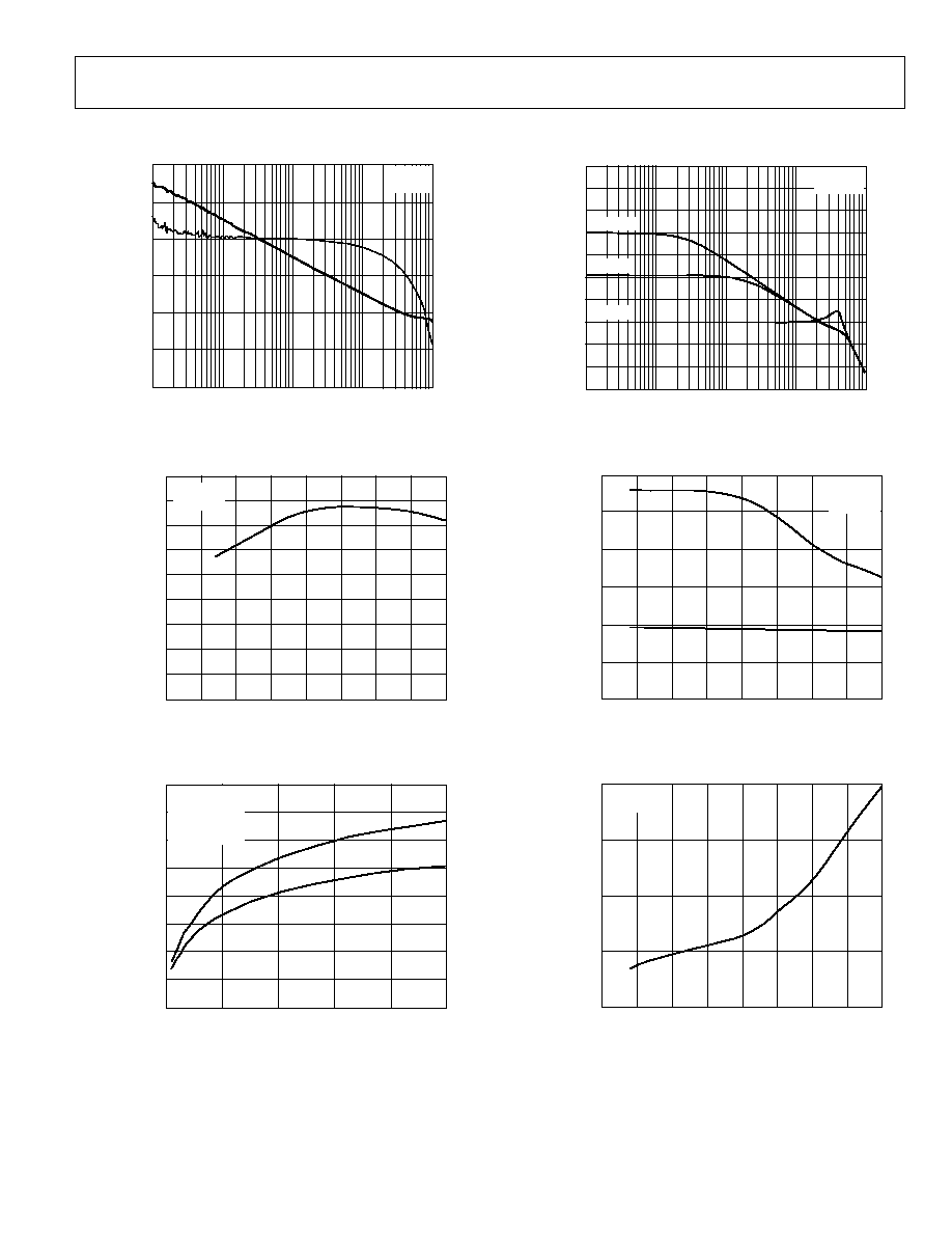
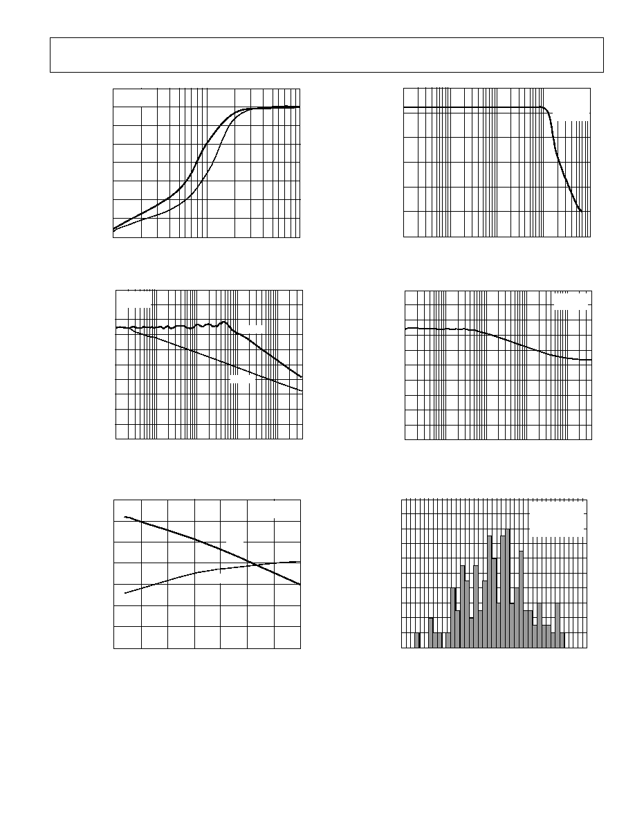
TYPICAL PERFORMANCE CHARACTERISTIC
FREQUENCY (Hz)
OP
E
N
-
L
OO
P
GA
IN
(
d
B
)
1k
40
20
60
80
10k
1M
10M
100k
20
40
0
V
S
= ±15V
T
A
= 25°C
P
HAS
E
(
D
eg
r
e
e
)
45
135
45
90
0
90
180
06
278
-
00
3
Figure 3. AD8682 Open-Loop Gain and Phase vs. Frequency
TEMPERATURE (°C)
OP
E
N
-
L
OO
P
GA
IN
(
V
/m
V
)
75
0
5
35
45
25
100
125
25
15
25
10
20
30
40
75
50
0
50
V
S
= ±15V
R
L
= 10k
06
27
8-
0
04
Figure 4. AD8682 Open-Loop Gain vs. Temperature
LOAD CAPACITANCE (pF)
O
VER
SH
O
O
T
(
%
)
0
0
10
70
80
200
400
500
30
50
20
40
60
300
100
V
S
= ±15V
R
L
= 2k
V
IN
= 100mV p-p
A
VCL
= 1
T
A
= 25°C
+OS
OS
06
27
8-
0
05
Figure 5. Small Signal Overshoot vs. Load Capacitance
FREQUENCY (Hz)
C
L
OS
E
D
-
L
OO
P
GA
IN
(
d
B
)
1k
30
20
60
70
10k
1M
10M
100k
20
40
0
V
S
= ±15V
T
A
= 25°C
10
50
10
30
A
VCL
= 100
A
VCL
= 10
A
VCL
= 1
06
27
8-
0
06
Figure 6. AD8682 Closed-Loop Gain vs. Frequency
TEMPERATURE (°C)
SL
E
W
R
A
TE
(
V
/µs
)
75
0
5
30
25
100
125
25
15
25
10
V
S
= ±15V
R
L
= 10k
C
L
= 50pF
20
75
50
0
50
SR
+SR
06
27
8-
00
7
Figure 7. Slew Rate vs. Temperature
TEMPERATURE (°C)
I
NP
UT
BI
AS
CURRE
NT
(
p
A
)
75
0.1
1000
25
100
125
25
1
100
10
75
50
0
50
V
S
= ±15V
V
CM
= 0V
06
27
8-
00
8
Figure 8. AD8682 Input Bias Current vs. Temperature
AD8682/AD8684
Rev. 0 | Page 6 of 16
FREQUENCY (Hz)
V
O
L
T
AG
E
NO
I
S
E
DE
NS
I
T
Y
(
n
V
/
Hz
)
10
1
1000
100
10k
1k
100
10
V
S
= ±15V
T
A
= 25°C
06
27
8-
0
09
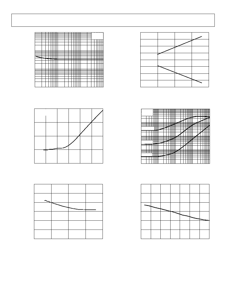
Figure 9. Voltage Noise Density vs. Frequency
COMMON-MODE VOLTAGE (V)
I
NP
UT
B
I
A
S
CURRE
NT
(
p
A
)
15
0.1
1000
10
15
5
1
100
10
5
0
10
V
S
= ±15V
T
A
= 25°C
06
27
8-
0
10
Figure 10. Input Bias Current vs. Common-Mode Voltage
SUPPLY VOLTAGE (V)
S
UP
P
L
Y
C
URRE
NT
(
µ
A
)
0
450
480
±20
±10
455
465
460
±15
±5
T
A
= 25°C
470
475
06
27
8-
0
11
Figure 11. AD8682 Supply Current vs. Supply Voltage
SUPPLY VOLTAGE (V)
O
U
T
P
U
T
VO
L
T
A
G
E SWI
N
G
(
V
)
0
20
20
±20
±10
15
5
10
±15
±5
T
A
= 25°C
R
L
= 10k
0
15
V
OH
V
OL
5
10
06
27
8-
01
2
Figure 12. Output Voltage Swing vs. Supply Voltage
FREQUENCY (Hz)
O
UT
P
UT
I
M
P
E
DAN
CE
(
)
1k
0.1
100
1000
10k
1M
100
100k
1
10
V
S
= ±15V
T
A
= 25°C
A
VCL
= 100
A
VCL
= 10
A
VCL
= 1
06
27
8-
01
3
Figure 13. Closed-Loop Output Impedance vs. Frequency
TEMPERATURE (°C)
S
U
PP
L
Y
C
U
R
R
EN
T
(µA
)
50
450
480
125
25
455
75
0
460
475
465
470
25
50
100
06
27
8-
0
14
Figure 14. AD8682 Supply Current vs. Temperature
AD8682/AD8684
Rev. 0 | Page 7 of 16
LOAD RESISTANCE ()
AB
S
O
L
U
T
E
O
UT
P
UT
V
O
L
T
AG
E
(
V
)
0
6
16
1k
10k
100
2
4
V
S
= ±15V
T
A
= 25°C
V
OL
V
OH
12
8
10
14
06
27
8-
01
5
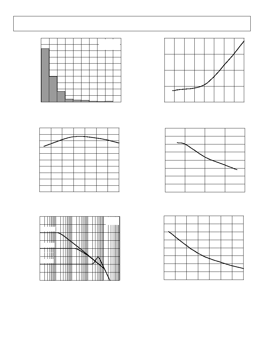
Figure 15. Absolute Output Voltage vs. Load Resistance
FREQUENCY (Hz)
P
S
R
R (
d
B)
1k
60
40
140
10k
1M
100
100k
0
20
40
20
60
100
120
80
PSRR
+PSRR
V
S
= ±15V
T
A
= 25°C
06
27
8-
0
16
Figure 16. AD8682 PSRR vs. Frequency
TEMPERATURE (°C)
SH
O
R
T
-
CI
RCUI
T
CURRE
NT
(
m
A)
50
0
14
125
25
4
75
0
6
12
8
10
25
50
100
2
SINK
SOURCE
V
S
= ±15V
T
A
= 25°C
06
27
8-
0
17
Figure 17. AD8682 Short-Circuit Current vs. Temperature
FREQUENCY (Hz)
MA
XI
MU
M O
U
TPU
T
SW
I
N
G
(V
p
-
p
)
100
0
5
25
30
1k
100k
1M
10k
15
20
10
V
S
= ±15V
T
A
= 25°C
R
L
= 10k
A
VCL
= 1
06
27
8-
0
18
Figure 18. Maximum Output Swing vs. Frequency
FREQUENCY (Hz)
CM
RR (
d
B
)
1k
60
40
140
10k
1M
100
100k
0
20
40
20
60
100
120
80
V
S
= ±15V
T
A
= 25°C
06
27
8-
0
19
Figure 19. AD8682 CMRR vs. Frequency
20
18
16
14
12
10
8
6
4
2
0
UNI
T
S
1.0 0.8 0.6
0.4 0.2
0
0.2
0.4
0.6
0.8
1.0
V
OS
(µV)
06
27
8-
02
0
V
S
= ±15V
T
A
= 25°C
100 ×AD8682
(200 OP AMPS)
Figure 20. AD8682 V
OS
Distribution
AD8682/AD8684
Rev. 0 | Page 8 of 16
TCV
OS
(µV/°C)
UNI
T
S
0
0
400
20
80
16
120
160
40
28
32
36
24
200
280
320
360
240
4
12
8
V
S
= ±15V
300 × OP282
(600 OP AMPS)
06
27
8-
0
21
Figure 21. AD8682 TCV
OS
Distribution SOIC_N Package
50
45
40
35
30
25
20
15
10
5
0
OP
E
N
-
L
OO
P
GA
IN
(
V
/m
V
)
50
25
0
25
50
75
100
125
TEMPERATURE (°C)
06
27
8-
02
2
Figure 22. AD8684 Open-Loop Gain vs. Temperature
FREQUENCY (Hz)
1k
10k
100k
1M
100M
10M
60
CL
O
S
E
D
-
L
O
O
P G
A
I
N
(
d
B)
40
20
10
0
50
30
10
20
V
S
= ±15V
T
A
= 25°C
06
27
8-
0
23
A
VCL
= 10
A
VCL
= 1
A
VCL
= 100
Figure 23. AD8684 Closed-Loop Gain vs. Frequency
06
27
8-
02
4
1000
100
10
1
0.1
I
NP
UT
BI
AS
CU
RRE
N
T
(
p
A)
50
25
0
25
50
75
100
125
TEMPERATURE (°C)
75
Figure 24. AD8684 Input Bias Current vs. Temperature
06
27
8-
02
5
950
945
940
930
925
920
915
910
S
UP
P
L
Y
CUR
RE
NT
(
µ
A)
0
10
20
30
SUPPLY VOLTAGE (V)
935
40
Figure 25. AD8684 Relative Supply Current vs. Supply Voltage
06
278
-
02
6
950
945
940
935
930
925
920
915
910
50
25
0
25
50
75
100
125
S
UP
P
L
Y
C
URRE
N
T
(
µ
A
)
TEMPERATURE (°C)
Figure 26. AD8684 Supply Current vs. Temperature
AD8682/AD8684
Rev. 0 | Page 9 of 16
1k
10k
100k
1M
10M
FREQUENCY (Hz)
PSRR+
PSRR
V
S
= ±15V
140
120
100
80
60
40
20
0
P
S
RR (
d
B)
06
27
8-
0
27
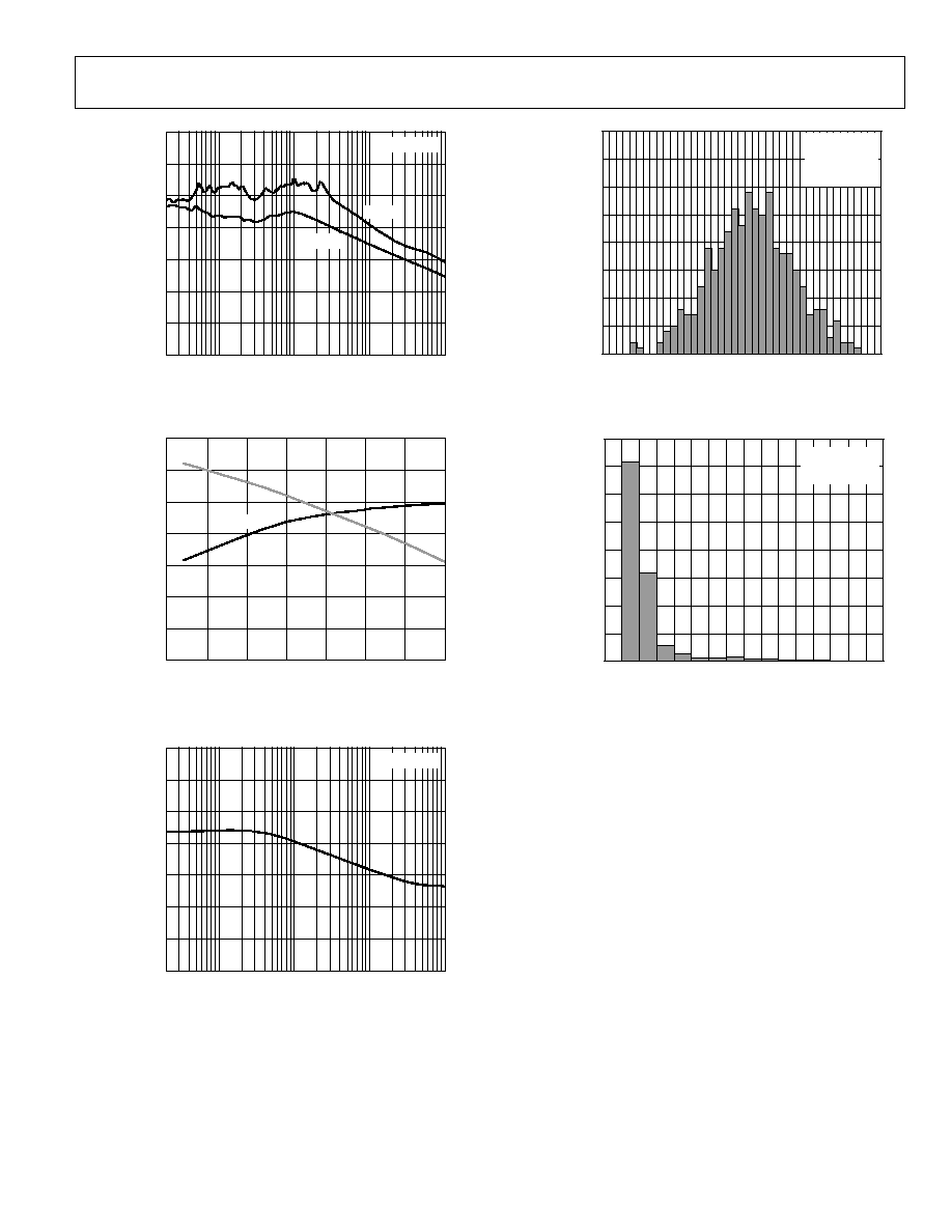
Figure 27. AD8684 PSRR vs. Frequency
14
12
10
8
6
4
2
0
S
HO
R
T
-
CI
RCUI
T
CU
RRE
NT
(
m
A)
50
25
0
25
50
75
100
TEMPERATURE (°C)
06
27
8-
0
28
125
SINK
SOURCE
Figure 28. AD8684 Short-Circuit Current vs. Temperature
1k
10k
100k
1M
10M
FREQUENCY (Hz)
V
S
= ±15V
140
120
100
80
60
40
20
0
CM
RR (
d
B)
06
27
8-
0
29
Figure 29. AD8684 CMRR vs. Frequency
V
S
= ±15V
T
A
= 25°C
100 × AD8684
(400 OP AMPS)
40
35
30
25
20
15
10
5
0
UN
I
T
S
1.0 0.8 0.6
1.0
V
OS
(µV)
06
27
8-
0
30
0.4 0.2
0
0.2
0.4
0.6
0.8
Figure 30. AD8684 V
OS
Distribution Package
06
27
8-
0
31
V
S
= ±15V
300 × OP282
(1200 OP AMPS)
800
700
600
500
400
300
200
100
0
UN
I
T
S
TCV
OS
(µV/°C)
24
60
56
52
48
44
40
36
32
28
20
16
12
8
4
0
Figure 31. AD8684 TCV
OS
Distribution Package
AD8682/AD8684
Rev. 0 | Page 10 of 16
APPLICATIONS INFORMATION
The AD8682 and AD8684 are dual and quad JFET op amps that
are optimized for high speed at low power. This combination
makes these amplifiers excellent choices for battery-powered or
low power applications that require above average performance.
Applications benefiting from this performance combination
include telecommunications, geophysical exploration, portable
medical equipment, and navigational instrumentation.
HIGH-SIDE SIGNAL CONDITIONING
There are many applications requiring the sensing of signals near
the positive rail. The AD8682 and the AD8684 were tested and
are guaranteed over a common-mode range (-11 V V
CM
+15 V) that includes the positive supply.
The AD8682/AD8684 are commonly used in the sensing of
power supply currents and in current sensing applications, such
as the partial circuit shown in Figure 32. In this circuit, the
voltage drop across a low value resistor, such as the 0.1 shown
here, is amplified and compared to 7.5 V. The output can then
be used for current limiting.
1/2
AD8682
100k
500k
100k
500k
0.1
15V
R
L
0
627
8-
0
42
Figure 32. High-Side Signal Conditioning
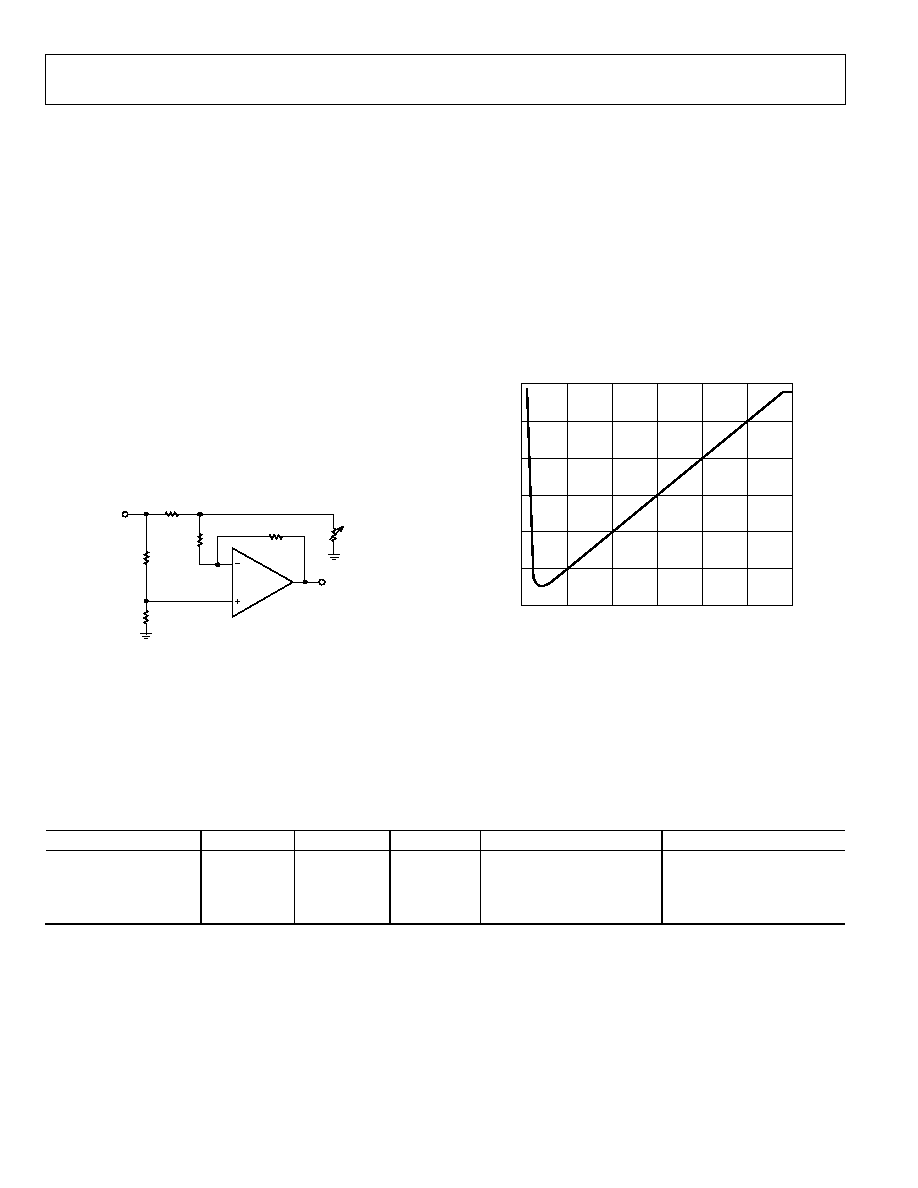
PHASE INVERSION
Most JFET input amplifiers invert the phase of the input signal
if either input exceeds the input common-mode range. For the
AD8682/AD8684, negative signals in excess of approximately
14 V cause phase inversion. This is caused by saturation of the
input stage leading to the forward-biasing of a drain-gate diode.
A simple fix for this in noninverting applications is to place
a resistor in series with the noninverting input. This limits the
amount of current through the forward-biased diode and prevents
shutting down of the output stage. For the AD8682/AD8684,
a value of 200 k has been found to work; however, it adds
a significant amount of noise.
15
10
5
0
5
10
15
V
OU
T
15
10
5
0
5
10
15
V
IN
06
27
8-
04
3
Figure 33. AD8682 Phase Reversal
ACTIVE FILTERS
The wide bandwidth and high slew rates of the AD8682/AD8684
make either one an excellent choice for many filter applications.
There are many active filter configurations, but the four most
popular configurations are: Butterworth, elliptical, Bessel, and
Chebyshev. Each type has a response that is optimized for a
given characteristic, as shown in Table 4.
Table 4.
Type
Selectivity
Overshoot
Phase
Amplitude (Pass Band)
Amplitude (Stop Band)
Butterworth Moderate
Good
Maximum
flat
Chebyshev Good
Moderate
Nonlinear
Equal
ripple
Elliptical
Best
Poor
Equal ripple
Equal ripple
Bessel (Thompson)
Poor
Best
Linear
AD8682/AD8684
Rev. 0 | Page 11 of 16
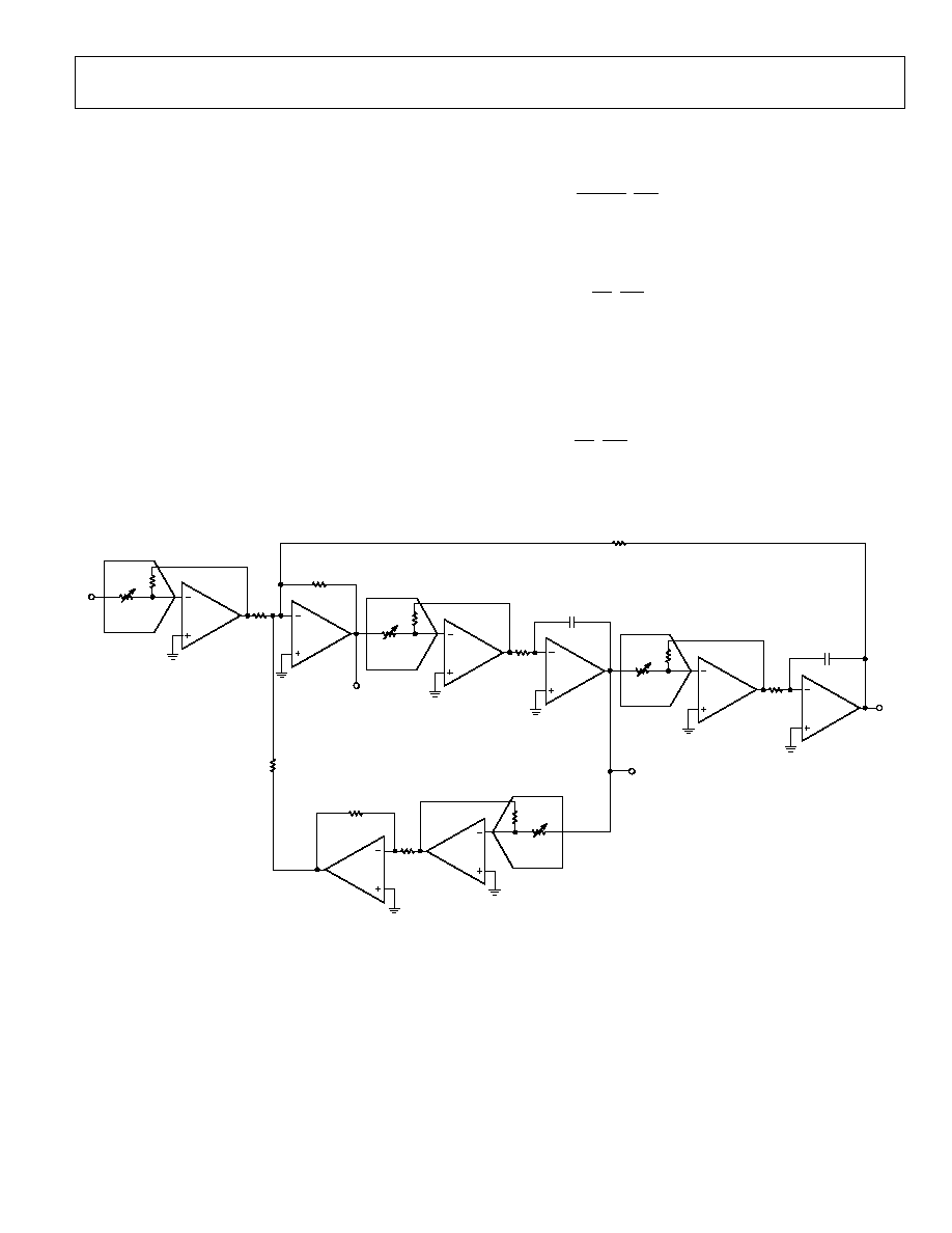
PROGRAMMABLE STATE VARIABLE FILTER
The circuit shown in Figure 34 can be used to accurately program
the Q; the cutoff frequency, f
C
; and the gain of a 2-pole state
variable filter. The AD8684 has been used in this design because
of its high bandwidth, low power, and low noise. This circuit takes
only three packages to build because of the quad configuration
of the op amps and DACs.
The DACs shown are used in voltage mode; therefore, many
values are dependent on the accuracy of the DAC only and not
on the absolute values of the DAC resistive ladders. As a result, this
makes the circuit unusually accurate for a programmable filter.
Adjusting DAC 1 changes the signal amplitude across R1; therefore,
the DAC attenuation × R1 determines the amount of signal current
that charges the integrating capacitor, C1.
This cutoff frequency can be expressed as
=
256
2
1
D1
R1C1
fc
where D1 is the digital code for the DAC.
The gain of this circuit is set by adjusting D3. The gain equation is
=
256
D3
R5
R4
Gain
DAC 2 is used to set the Q of the circuit. Adjusting this DAC
controls the amount of feedback from the band-pass node to
the input summing node. Note that the digital value of the
DAC is in the numerator; therefore, zero code is not a valid
operating point.
=
D2
R3
R2
Q
256
1/4
AD8684
1/4
DAC8408
R5
2k
R4
2k
1/4
AD8684
1/4
AD8684
1/4
DAC8408
R1
2k
C1
1000pF
1/4
AD8684
1/4
AD8684
1/4
DAC8408
R1
2k
C1
1000pF
1/4
AD8684
1/4
DAC8408
R2
2k
R3
2k
1/4
AD8684
1/4
AD8684
R6
2k
HIGH PASS
BAND PASS
LOW
PASS
V
IN
R7
2k
0
62
78-
04
4
Figure 34. Programmable State Variable Filter
AD8682/AD8684
Rev. 0 | Page 12 of 16
OUTLINE DIMENSIONS
CONTROLLING DIMENSIONS ARE IN MILLIMETERS; INCH DIMENSIONS
(IN PARENTHESES) ARE ROUNDED-OFF MILLIMETER EQUIVALENTS FOR
REFERENCE ONLY AND ARE NOT APPROPRIATE FOR USE IN DESIGN.
COMPLIANT TO JEDEC STANDARDS MS-012-AA
06
05
06
-
A
0.25 (0.0098)
0.17 (0.0067)
1.27 (0.0500)
0.40 (0.0157)
0.50 (0.0196)
0.25 (0.0099)
45°
8°
0°
1.75 (0.0688)
1.35 (0.0532)
SEATING
PLANE
0.25 (0.0098)
0.10 (0.0040)
4
1
8
5
5.00 (0.1968)
4.80 (0.1890)
4.00 (0.1574)
3.80 (0.1497)
1.27 (0.0500)
BSC
6.20 (0.2440)
5.80 (0.2284)
0.51 (0.0201)
0.31 (0.0122)
COPLANARITY
0.10
Figure 35. 8-Lead Standard Small Outline Package [SOIC_N]
Narrow Body
(R-8)
Dimensions shown in millimeters and (inches)
COMPLIANT TO JEDEC STANDARDS MO-187-AA
0.80
0.60
0.40
8°
0°
4
8
1
5
PIN 1
0.65 BSC
SEATING
PLANE
0.38
0.22
1.10 MAX
3.20
3.00
2.80
COPLANARITY
0.10
0.23
0.08
3.20
3.00
2.80
5.15
4.90
4.65
0.15
0.00
0.95
0.85
0.75
Figure 36. 8-Lead Mini Small Outline Package [MSOP]
(RM-8)
Dimensions shown in millimeters
AD8682/AD8684
Rev. 0 | Page 13 of 16
CONTROLLING DIMENSIONS ARE IN MILLIMETERS; INCH DIMENSIONS
(IN PARENTHESES) ARE ROUNDED-OFF MILLIMETER EQUIVALENTS FOR
REFERENCE ONLY AND ARE NOT APPROPRIATE FOR USE IN DESIGN.
COMPLIANT TO JEDEC STANDARDS MS-012-AB
06
06
06
-
A
14
8
7
1
6.20 (0.2441)
5.80 (0.2283)
4.00 (0.1575)
3.80 (0.1496)
8.75 (0.3445)
8.55 (0.3366)
1.27 (0.0500)
BSC
SEATING
PLANE
0.25 (0.0098)
0.10 (0.0039)
0.51 (0.0201)
0.31 (0.0122)
1.75 (0.0689)
1.35 (0.0531)
0.50 (0.0197)
0.25 (0.0098)
1.27 (0.0500)
0.40 (0.0157)
0.25 (0.0098)
0.17 (0.0067)
COPLANARITY
0.10
8°
0°
45°
Figure 37. 14-Lead Standard Small Outline Package [SOIC_N]
Narrow Body
(R-14)
Dimensions shown in millimeters and (inches)
4.50
4.40
4.30
14
8
7
1
6.40
BSC
PIN 1
5.10
5.00
4.90
0.65
BSC
SEATING
PLANE
0.15
0.05
0.30
0.19
1.20
MAX
1.05
1.00
0.80
0.20
0.09
8°
0°
0.75
0.60
0.45
COPLANARITY
0.10
COMPLIANT TO JEDEC STANDARDS MO-153-AB-1
Figure 38. 14-Lead Thin Shrink Small Outline Package [TSSOP]
(RU-14)
Dimensions shown in millimeters
ORDERING GUIDE
Model
Temperature Range
Package Description
Package Option
Branding
AD8682ARZ
1
-40°C to +85°C
8-Lead SOIC_N
R-8
AD8682ARZ-REEL
1
-40°C to +85°C
8-Lead SOIC_N
R-8
AD8682ARZ-REEL7
1
-40°C to +85°C
8-Lead SOIC_N
R-8
AD8682ARMZ-R2
1
-40°C to +85°C
8-Lead MSOP
RM-8
A1K
AD8682ARMZ-REEL
1
-40°C to +85°C
8-Lead MSOP
RM-8
A1K
AD8684ARZ
1
-40°C to +85°C
14-Lead SOIC_N
R-14
AD8684ARZ-REEL
1
-40°C to +85°C
14-Lead SOIC_N
R-14
AD8684ARZ-REEL7
1
-40°C to +85°C
14-Lead SOIC_N
R-14
AD8684ARUZ
1
-40°C to +85°C
14-Lead TSSOP
RU-14
AD8684ARUZ_REEL
1
-40°C to +85°C
14-Lead TSSOP
RU-14
1
Z= Pb-free part.

AD8682/AD8684
Rev. 0 | Page 14 of 16
NOTES

AD8682/AD8684
Rev. 0 | Page 15 of 16
NOTES

AD8682/AD8684
Rev. 0 | Page 16 of 16
NOTES
©2006 Analog Devices, Inc. All rights reserved. Trademarks and
registered trademarks are the property of their respective owners.
D06278-0-10/06(0)
Document Outline
- þÿ
- þÿ
- PIN CONFIGURATIONS
- þÿ
- þÿ
- þÿ
- þÿ
- þÿ
- þÿ
- þÿ