 | ÐлекÑÑоннÑй компоненÑ: AD9397 | СкаÑаÑÑ:  PDF PDF  ZIP ZIP |
Äîêóìåíòàöèÿ è îïèñàíèÿ www.docs.chipfind.ru
DVI Display Interface
AD9397
Rev. 0
Information furnished by Analog Devices is believed to be accurate and reliable. However, no
responsibility is assumed by Analog Devices for its use, nor for any infringements of patents or other
rights of third parties that may result from its use. Specifications subject to change without notice. No
license is granted by implication or otherwise under any patent or patent rights of Analog Devices.
Trademarks and registered trademarks are the property of their respective owners.
One Technology Way, P.O. Box 9106, Norwood, MA 02062-9106, U.S.A.
Tel: 781.329.4700
www.analog.com
Fax: 781.461.3113
© 2005 Analog Devices, Inc. All rights reserved.
FEATURES
DVI interface
Supports high-bandwidth digital content protection
RGB to YCbCr 2-way color conversion
1.8 V/3.3 V power supply
100-lead, Pb-free LQFP
RGB and YCbCr output formats
Digital video interface
DVI 1.0
150 MHz DVI receiver
Supports high-bandwidth digital content protection
(HDCP 1.1)
APPLICATIONS
Advanced TVs
HDTVs
Projectors
LCD monitors
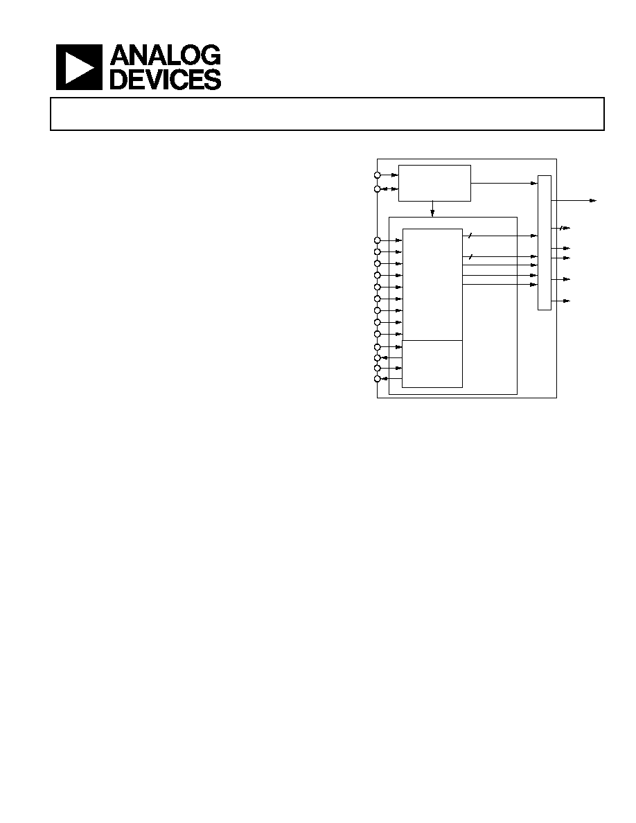
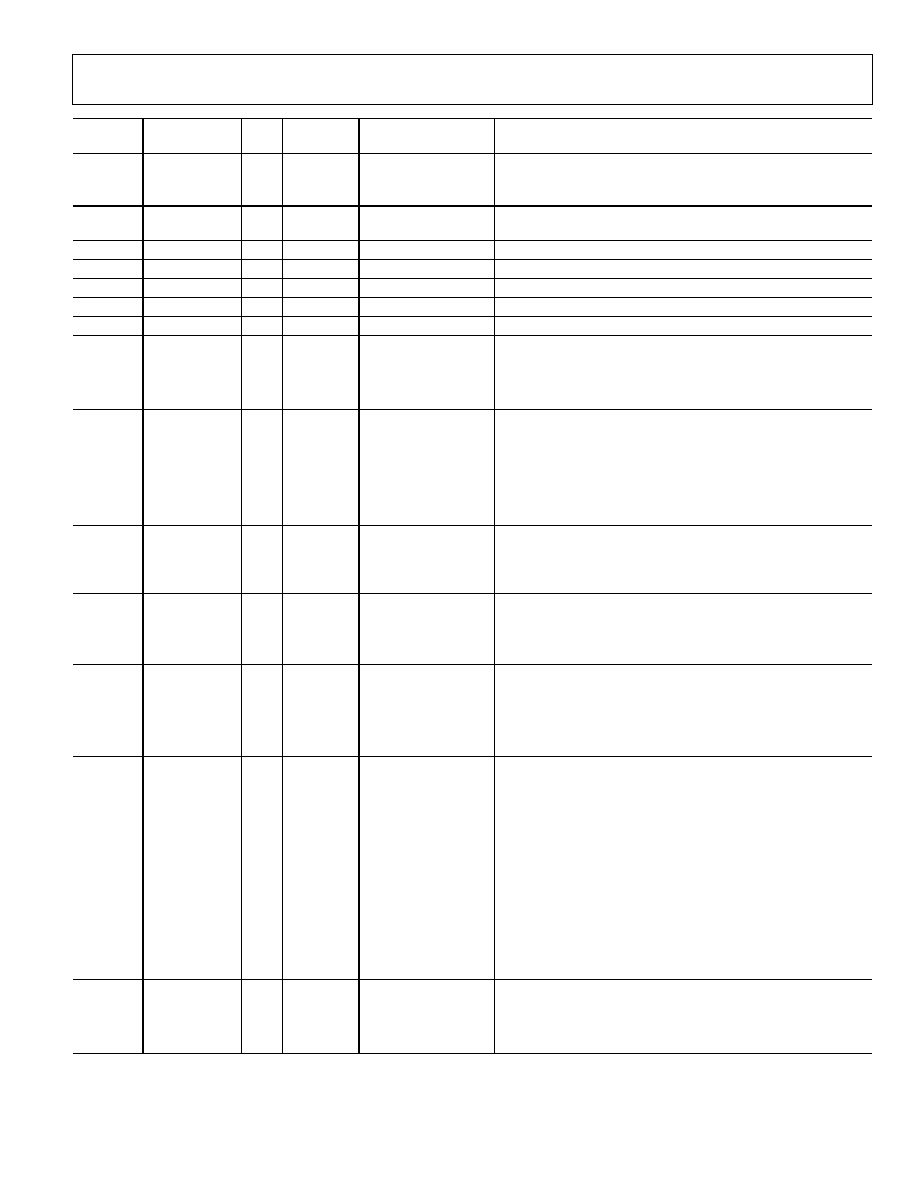
FUNCTIONAL BLOCK DIAGRAM
05691-001
DATACK
DE
VSYNC
2
2
DATACK
HSOUT
SOGOUT
DE
R/G/B 8 × 3
OR YCbCr
YCbCr (4:2:2
OR 4:4:4)
AD9397
Rx1+
Rx1
Rx2+
Rx2
RxC+
RxC
RTERM
Rx0+
Rx0
HSYNC
R/G/B 8 × 3
RGB
Y
C
bCr M
A
TRI
X
MCL
DVI RECEIVER
SERIAL REGISTER
AND
POWER MANAGEMENT
SCL
SDA
MDA
VSOUT
DIGITAL INTERFACE
DDCSCL
DDCSDA
HDCP
Figure 1.
GENERAL DESCRIPTION
The AD9397 is a digital visual interface (DVI) receiver
integrated on a single chip. Also included is support for high
bandwidth digital content protection (HDCP) with internal key
storage.
The AD9397 contains a DVI 1.0-compatible receiver and
supports all HDTV formats (up to 1080p and 720p) and display
resolutions up to SXGA (1280 × 1024 @ 80 Hz). The receiver
features an intrapair skew tolerance of up to one full clock cycle.
With the inclusion of HDCP, displays can receive encrypted
video content. The AD9397 allows for authentication of a video
receiver, decryption of encoded data at the receiver, and
renewability of that authentication during transmission as
specified by the HDCP 1.1 protocol.
Fabricated in an advanced CMOS process, the AD9397 is
provided in a space-saving, 100-lead, surface-mount, Pb-free
plastic LQFP and is specified over the 0°C to 70°C temperature
range.

AD9397
Rev. 0 | Page 2 of 28
TABLE OF CONTENTS
Features .............................................................................................. 1
Applications....................................................................................... 1
Functional Block Diagram .............................................................. 1
General Description ......................................................................... 1
Revision History ............................................................................... 2
Specifications..................................................................................... 3
Electrical Characteristics............................................................. 3
Digital Interface Electrical Characteristics ............................... 4
Absolute Maximum Ratings............................................................ 6
Explanation of Test Levels ........................................................... 6
ESD Caution.................................................................................. 6
Pin Configuration and Function Descriptions............................. 7
Design Guide................................................................................... 10
General Description................................................................... 10
Digital Inputs .............................................................................. 10
Serial Control Port ..................................................................... 10
Output Signal Handling............................................................. 10
Power Management.................................................................... 10
Timing.............................................................................................. 11
HSYNC Timing .......................................................................... 11
VSYNC Filter and Odd/Even Fields ........................................ 11
DVI Receiver............................................................................... 11
DE Generator.............................................................................. 11
4:4:4 to 4:2:2 Filter ...................................................................... 12
Output Data Formats................................................................. 12
2-Wire Serial Register Map ........................................................... 13
2-Wire Serial Control Register Details ........................................ 18
Chip Identification ..................................................................... 18
BT656 Generation ...................................................................... 20
Macrovision................................................................................. 21
Color Space Conversion ............................................................ 21
2-Wire Serial Control Port ............................................................ 23
Data Transfer via Serial Interface............................................. 23
Serial Interface Read/Write Examples ..................................... 24
PCB Layout Recommendations.................................................... 25
Power Supply Bypassing ............................................................ 25
Outputs (Both Data and Clocks).............................................. 25
Digital Inputs .............................................................................. 25
Color Space Converter (CSC) Common Settings...................... 26
Outline Dimensions ....................................................................... 28
Ordering Guide .......................................................................... 28
REVISION HISTORY
10/05--Revision 0: Initial Version
AD9397
Rev. 0 | Page 3 of 28
SPECIFICATIONS
ELECTRICAL CHARACTERISTICS
V
DD
, V
D
= 3.3 V, DV
DD
= PV
DD
= 1.8 V, ADC clock = maximum.
Table 1.
AD9397KSTZ-100 AD9397KSTZ-150
Parameter
Temp
Test
Level
Min Typ
Max
Min Typ
Max
Unit
RESOLUTION
8
8
Bits
Data-to-Clock
Skew
Full
IV
-0.5 +2.0
-0.5 +2.0
ns
Serial
Port
Timing
t
BUFF
Full
VI
4.7
4.7
s
t
STAH
Full
VI
4.0
4.0
s
t
DHO
Full
VI 0
0
s
t
DAL
Full
VI
4.7
4.7
s
t
DAH
Full
VI
4.0
4.0
s
t
DSU
Full
VI
250
250
ns
t
STASU
Full
VI
4.7
4.7
s
t
STOSU
Full
VI
4.0
4.0
s
DIGITAL
INPUTS
(5
V
TOLERANT)
Input Voltage, High (V
IH
) Full
VI
2.6
2.6
V
Input Voltage, Low (V
IL
) Full
VI
0.8
0.8
V
Input Current, High (I
IH
)
Full V
-82
-82
A
Input Current, Low (I
IL
) Full
V 82
82
A
Input
Capacitance
25°C
V 3
3
pF
DIGITAL
OUTPUTS
Output Voltage, High (V
OH
) Full
VI
V
DD
- 0.1
V
DD
- 0.1
V
Output Voltage, Low (V
OL
)
Full
VI
0.4
0.4
V
Duty Cycle, DATACK
Full
V
45
50
55
45
50
55
%
Output
Coding
Binary
Binary
POWER
SUPPLY
V
D
Supply
Voltage
Full
IV
3.15 3.3
3.47
3.15 3.3
3.47
V
DV
DD
Supply
Voltage
Full
IV
1.7 1.8
1.9
1.7 1.8
1.9
V
V
DD
Supply
Voltage
Full
IV
1.7 3.3
3.47
1.7 3.3
3.47
V
PV
DD
Supply
Voltage
Full
IV
1.7 1.8
1.9
1.7 1.8
1.9
V
I
D
Supply Current (V
D
) 25°C
VI 260
300
330
mA
I
DVDD
Supply Current (DV
DD
)
25°C
VI 45
60
85
mA
I
DD
Supply Current (V
DD
)
1
25°C VI
37
100
2
130
2
mA
IP
VDD
Supply Current (P
VDD
)
25°C
VI 10
15
20
mA
Total
Power
Full
VI 1.1
1.4
1.15
1.4
W
Power-Down
Dissipation
Full
VI 130
130
mW
THERMAL
CHARACTERISTICS
JA
Junction to Ambient
V
35
35
°C/W
1
DATACK load = 15 pF, data load = 5 pF.
2
Specified current and power values with a worst-case pattern (on/off).
AD9397
Rev. 0 | Page 4 of 28
DIGITAL INTERFACE ELECTRICAL CHARACTERISTICS
V
DD
= V
D
= 3.3 V, DV
DD
= PV
DD
= 1.8 V, ADC clock = maximum.
Table 2.
Test
AD9397KSTZ-100
AD9397KSTZ-150
Parameter Level
Conditions
Min
Typ
Max
Min
Typ
Max
Unit
RESOLUTION
8
8
Bit
DC DIGITAL I/O SPECIFICATIONS
High Level Input Voltage, (V
IH
) VI
2.5
2.5
V
Low Level Input Voltage, (V
IL
) VI
0.8
0.8
V
High Level Output Voltage, (V
OH
) VI
V
DD
- 0.1
V
Low Level Output Voltage, (V
OL
) VI
V
DD
- 0.1
0.1
0.1
V
DC SPECIFICATIONS
Output High Level
IV
Output drive = high
36
36
mA
I
OHD
, (V
OUT
= V
OH
)
IV
Output drive = low
24
24
mA
Output Low Level
IV
Output drive = high
12
12
mA
I
OLD
, (V
OUT
= V
OL
)
IV
Output drive = low
8
8
mA
DATACK High Level
IV
Output drive = high
40
40
mA
V
OHC
, (V
OUT
= V
OH
)
IV
Output drive = low
20
20
mA
DATACK Low Level
IV
Output drive = high
30
30
mA
V
OLC
, (V
OUT
= V
OL
)
IV
Output drive = low
15
15
mA
Differential Input Voltage, Single-Ended
Amplitude
IV
75 700
75
700
mV
POWER SUPPLY
V
D
Supply Voltage
IV
3.15
3.3
3.47
3.15
3.3
3.47
V
V
DD
Supply Voltage
IV
1.7
3.3
347
1.7
3.3
347
V
DV
DD
Supply Voltage
IV
1.7
1.8
1.9
1.7
1.8
1.9
V
PV
DD
Supply Voltage
IV
1.7
1.8
1.9
1.7
1.8
1.9
V
I
VD
Supply Current (Typical Pattern)
1
V
80
100
80
110
mA
I
VDD
Supply Current (Typical Pattern)
2
V
40
100
3
55
175
3
mA
I
DVDD
Supply Current (Typical Pattern)
1, 4
V
88
110
110
145
mA
I
PVDD
Supply Current (Typical Pattern)
1
V
26
35
30
40
mA
Power-Down Supply Current (I
PD
) VI
130
130
mA
AD9397
Rev. 0 | Page 5 of 28
Test
AD9397KSTZ-100
AD9397KSTZ-150
Parameter Level
Conditions
Min
Typ
Max
Min
Typ
Max
Unit
AC SPECIFICATIONS
Intrapair (+ to -) Differential Input Skew
(T
DPS
)
IV
360
ps
Channel to Channel Differential Input
Skew (T
CCS
)
IV
6 Clock
Period
Low-to-High Transition Time for Data
and Controls (D
LHT
)
IV
Output drive = high;
C
L
= 10 pF
900
ps
IV
Output drive = low;
C
L
= 5 pF
1300
ps
Low-to-High Transition Time for DATACK
(D
LHT
)
IV
Output drive = high;
C
L
= 10 pF
650
ps
IV
Output drive = low;
C
L
= 5 pF
1200
ps
High-to-Low Transition Time for Data
and Controls (D
HLT
)
IV
Output drive = high;
C
L
= 10 pF
850
ps
IV
Output drive = low;
C
L
= 5 pF
1250
ps
High-to-Low Transition Time for DATACK
(D
HLT
)
IV
Output drive = high;
C
L
= 10 pF
800
ps
IV
Output drive = low;
C
L
= 5 pF
1200
ps
Clock to Data Skew
5
(T
SKEW
) IV
-0.5
+2.0
-0.5
+2.0
ns
Duty Cycle, DATACK
5
IV
45 50
55
%
DATACK Frequency (F
CIP
) VI
20
150
MHz
1
The typical pattern contains a gray scale area, output drive = high. Worst-case pattern is alternating black and white pixels.
2
The typical pattern contains a gray scale area, output drive = high.
3
Specified current and power values with a worst-case pattern (on/off).
4
DATACK load = 10 pF, data load = 5 pF.
5
Drive strength = high.
AD9397
Rev. 0 | Page 6 of 28
ABSOLUTE MAXIMUM RATINGS
Table 3.
Stresses above those listed under Absolute Maximum Ratings
may cause permanent damage to the device. This is a stress
rating only; functional operation of the device at these or any
other conditions above those indicated in the operational
section of this specification is not implied. Exposure to absolute
maximum rating conditions for extended periods may affect
device reliability.
EXPLANATION OF TEST LEVELS
Table 4.
Level Test
I
100% production tested.
II
100% production tested at 25°C and sample tested at
specified temperatures.
III
Sample tested only.
IV
Parameter is guaranteed by design and
characterization testing.
V
Parameter is a typical value only.
VI
100% production tested at 25°C; guaranteed by design
and characterization testing.
ESD CAUTION
ESD (electrostatic discharge) sensitive device. Electrostatic charges as high as 4000 V readily accumulate on
the human body and test equipment and can discharge without detection. Although this product features
proprietary ESD protection circuitry, permanent damage may occur on devices subjected to high energy
electrostatic discharges. Therefore, proper ESD precautions are recommended to avoid performance
degradation or loss of functionality.
Parameter Rating
V
D
3.6 V
V
DD
3.6 V
DV
DD
1.98 V
PV
DD
1.98 V
Analog Inputs
V
D
to 0.0 V
Digital Inputs
5 V to 0.0 V
Digital Output Current
20 mA
Operating Temperature Range
-25°C to + 85°C
Storage Temperature Range
-65°C to + 150°C
Maximum Junction Temperature
150°C
Maximum Case Temperature
150°C
AD9397
Rev. 0 | Page 7 of 28
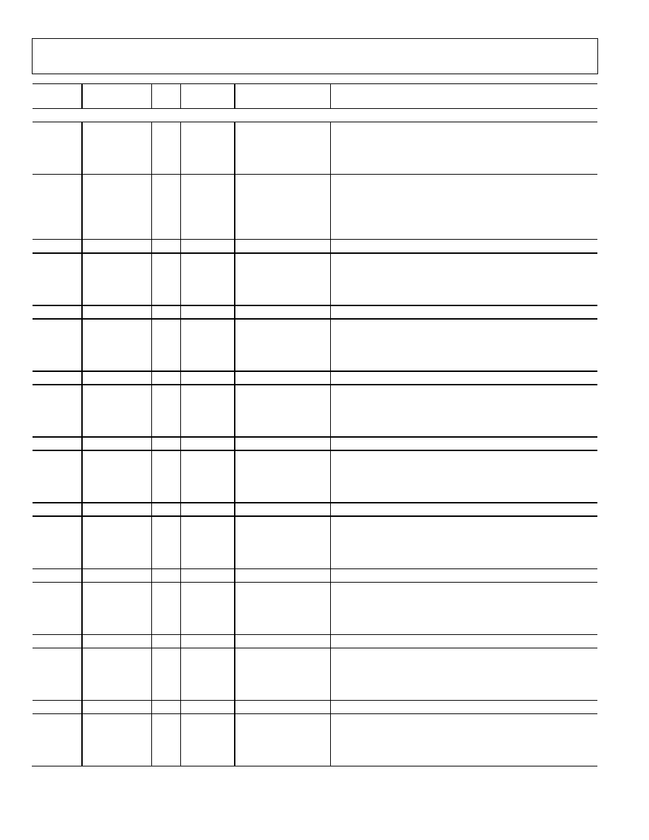
PIN CONFIGURATION AND FUNCTION DESCRIPTIONS
05691-002
V
DD
RE
D 0
RE
D 1
RE
D 2
RE
D 3
RE
D 4
RE
D 5
RE
D 6
RE
D 7
GND
V
DD
DATAC
K
DE
HS
OUT
NC
VSOU
T
FIELD
SD
A
SC
L
P
W
RDN
V
D
NC
GND
NC
V
D
26
CTL1
27
CTL0
28
NC
29
GND
30
DV
DD
31
GND
32
DV
DD
33
V
D
34
R
x0
35
R
x0+
36
GND
37
R
x1
38
R
x1+
39
GND
2
GREEN 7
3
GREEN 6
4
GREEN 5
7
GREEN 2
6
GREEN 3
5
GREEN 4
1
GND
8
GREEN 1
9
GREEN 0
10
V
DD
12
BLUE 7
13
BLUE 6
14
BLUE 5
15
BLUE 4
16
BLUE 3
17
BLUE 2
18
BLUE 1
19
BLUE 0
20
NC
21
NC
22
NC
23
NC
24
CTL3
25
CTL2
11
GND
74
NC
GND
73
NC
72
V
D
69
GND
70
NC
71
NC
75
68
NC
67
V
D
66
NC
64
NC
63
NC
62
NC
61
NC
60
NC
59
PV
DD
58
GND
57
NC
56
PV
DD
55
GND
54
PV
DD
53
GND
52
MDA
51
MCL
65
GND
40
R
x2
41
R
x2+
42
GND
43
Rx
C+
44
Rx
C
45
V
D
46
RTE
R
M
47
GND
48
DV
DD
49
DDCS
CL
50
DDCS
DA
100
99
98
97
96
95
94
93
92
91
90
89
88
87
86
85
84
83
82
81
80
79
78
77
76
PIN 1
AD9397
TOP VIEW
(Not to Scale)
NC = NO CONNECT
Figure 2. Pin Configuration
Table 5. Complete Pinout List
Pin Type
Pin No.
Mnemonic
Function
Value
INPUTS
81
PWRDN
Power-Down Control
3.3 V CMOS
DIGITAL VIDEO DATA INPUTS
35
Rx0+
Digital Input Channel 0 True
TMDS
34
Rx0-
Digital Input Channel 0 Complement
TMDS
38
Rx1+
Digital Input Channel 1 True
TMDS
37
Rx1-
Digital Input Channel 1 Complement
TMDS
41
Rx2+
Digital Input Channel 2 True
TMDS
40
Rx2-
Digital Input Channel 2 Complement
TMDS
DIGITAL VIDEO CLOCK INPUTS
43
RxC+
Digital Data Clock True
TMDS
44
RxC-
Digital Data Clock Complement
TMDS
OUTPUTS
92 to 99
RED [7:0]
Outputs of Red Converter, Bit 7 is MSB
V
DD
2 to 9
GREEN [7:0]
Outputs of Green Converter, Bit 7 is MSB
V
DD
12 to 19
BLUE [7:0]
Outputs of Blue Converter, Bit 7 is MSB
V
DD
89
DATACK
Data Output Clock
V
DD
87
HSOUT
HSYNC Output Clock (Phase-Aligned with DATACK)
V
DD
85
VSOUT
VSYNC Output Clock (Phase-Aligned with DATACK)
V
DD
84
O/E FIELD
Odd/Even Field Output
V
DD
27, 26, 25, 24
CTL(0 to 3)
Control 0, 1, 2, 3
V
DD
AD9397
Rev. 0 | Page 8 of 28
Pin Type
Pin No.
Mnemonic
Function
Value
POWER SUPPLY
80, 76, 72, 67,
45, 33
V
D
Analog Power Supply and DVI Terminators
3.3 V
100, 90, 10
V
DD
Output Power Supply
1.8 V to 3.3 V
59, 56, 54
PV
DD
PLL Power Supply
1.8 V
48, 32, 30
DV
DD
Digital Logic Power Supply
1.8 V
GND
Ground
0
V
CONTROL
83
SDA
Serial Port Data I/O
3.3 V CMOS
82
SCL
Serial Port Data Clock
3.3 V CMOS
HDCP
49
DDCSCL
HDCP Slave Serial Port Data Clock
3.3 V CMOS
50
DDCSDA
HDCP Slave Serial Port Data I/O
3.3 V CMOS
51
MCL
HDCP Master Serial Port Data Clock
3.3 V CMOS
52
MDA
HDCP Master Serial Port Data I/O
3.3 V CMOS
DATA ENABLE
88
DE
Data Enable
3.3 V CMOS
RTERM
46
RTERM
Sets Internal Termination Resistance
500
Table 6. Pin Function Descriptions
Pin Description
INPUTS
Rx0+
Digital Input Channel 0 True.
Rx0-
Digital Input Channel 0 Complement.
Rx1+
Digital Input Channel 1 True.
Rx1-
Digital Input Channel 1 Complement.
Rx2+
Digital Input Channel 2 True.
Rx2-
Digital input Channel 2 Complement.
These six pins receive three pairs of transition minimized differential signaling (TMDS ) pixel data
(at 10× the pixel rate) from a digital graphics transmitter.
RxC+
Digital Data Clock True.
RxC-
Digital Data Clock Complement.
This clock pair receives a TMDS clock at 1× pixel data rate.
PWRDN
Power-Down Control/Three-State Control.
The function of this pin is programmable via Register 0x26 [2:1].
RTERM
RTERM is the termination resistor used to drive the AD9397 internally to a precise 50 termination for
TMDS lines. This should be a 500
1% tolerance resistor.
OUTPUTS
HSOUT Horizontal
Sync
Output.
A reconstructed and phase-aligned version of the HSYNC input. Both the polarity and duration of this
output can be programmed via serial bus registers. By maintaining alignment with DATACK and Data,
data timing with respect to horizontal sync can always be determined.
VSOUT
Vertical Sync Output.
The separated VSYNC from a composite signal or a direct pass through of the VSYNC signal. The polarity
of this output can be controlled via the serial bus bit (Register 0x24 [6]).
FIELD
Odd/Even Field Bit for Interlaced Video. This output identifies whether the current field (in an interlaced
signal) is odd or even. The polarity of this signal is programmable via Register 0x24[4].
DE
Data Enable that defines valid video. Can be received in the signal or generated by the AD9397.
CTL(3-0)
Control 3, Control 2, Control 1, and Control 0 are output from the DVI stream. Refer to the DVI 1.0
specification for explanation.
SERIAL PORT
SDA
Serial Port Data I/O for Programming AD9397 Registers--I
2
C Address is 0x98.
SCL
Serial Port Data Clock for Programming AD9397 Registers.
DDCSDA
Serial Port Data I/O for HDCP Communications to Transmitter--I
2
C Address is 0x74 or 0x76.
DDCSCL
Serial Port Data Clock for HDCP Communications to Transmitter.
MDA
Serial Port Data I/O to EEPROM with HDCP Keys--I
2
C Address is 0xA0.
MCL
Serial Port Data Clock to EEPROM with HDCP Keys.

AD9397
Rev. 0 | Page 9 of 28
Pin Description
DATA OUTPUTS
RED [7:0]
Data Output, Red Channel.
GREEN [7:0]
Data Output, Green Channel.
BLUE [7:0]
Data Output, Blue Channel.
The main data outputs. Bit 7 is the MSB. The delay from pixel sampling time to output is fixed, but is
different if the color space converter is used. When the sampling time is changed by adjusting the phase
register, the output timing is shifted as well. The DATACK and HSOUT outputs are also moved, so the
timing relationship among the signals is maintained.
DATA CLOCK OUTPUT
DATACK
Data Clock Output.
This is the main clock output signal used to strobe the output data and HSOUT into external logic. Four
possible output clocks can be selected with Register 0x25 [7:6]. These are related to the pixel clock (1/2×
pixel clock, 1× pixel clock, 2× frequency pixel clock, and a 90° phase shifted pixel clock). They are
produced either by the internal PLL clock generator or EXTCLK and are synchronous with the pixel
sampling clock. The polarity of DATACK can also be inverted via Register 0x24 [0]. The sampling time of
the internal pixel clock can be changed by adjusting the phase register. When this is changed, the pixel-
related DATACK timing is shifted as well. The DATA, DATACK, and HSOUT outputs are all moved, so the
timing relationship among the signals is maintained.
POWER SUPPLY
1
V
D
(3.3 V)
Analog Power Supply.
These pins supply power to the ADCs and terminators. They should be as quiet and filtered as possible.
V
DD
(1.8 V to 3.3 V)
Digital Output Power Supply.
A large number of output pins (up to 27) switching at high speed (up to 150 MHz) generates many power
supply transients (noise). These supply pins are identified separately from the V
D
pins, so output noise
transferred into the sensitive analog circuitry can be minimized. If the AD9397 is interfacing with lower
voltage logic, V
DD
may be connected to a lower supply voltage (as low as 1.8 V) for compatibility.
PV
DD
(1.8 V)
Clock Generator Power Supply.
The most sensitive portion of the AD9397 is the clock generation circuitry. These pins provide power to
the clock PLL and help the user design for optimal performance. The designer should provide quiet,
noise-free power to these pins.
DV
DD
(1.8 V)
Digital Input Power Supply.
This supplies power to the digital logic.
GND Ground.
The ground return for all circuitry on chip. It is recommended that the AD9397 be assembled on a single
solid ground plane, with careful attention to ground current paths.
1
The supplies should be sequenced such that V
D
and V
DD
are never less than 300 mV below DV
DD
. At no time should DV
DD
be more than 300 mV greater than V
D
or V
DD
.
AD9397
Rev. 0 | Page 10 of 28
DESIGN GUIDE
GENERAL DESCRIPTION
The AD9397 is a fully integrated digital visual interface (DVI )
for receiving RGB or YUV signals for display on flat panel
monitors, projectors or PDPs. This interface is capable of
decoding HDCP-encrypted signals through connection to an
external EEPROM. The circuit is ideal for providing an
interface for HDTV monitors or as the front-end to high
performance video scan converters.
Implemented in a high performance CMOS process, the
interface can capture signals with pixel rates of up to 150 MHz.
The AD9397 includes all necessary input buffering, signal dc
restoration (clamping), offset and gain (brightness and contrast)
adjustment, pixel clock generation, sampling phase control, and
output data formatting. Included in the output formatting is a
color space converter (CSC), which accommodates any input
color space and can output any color space. All controls are
programmable via a 2-wire serial interface. Full integration of
these sensitive analog functions makes system design straight-
forward and less sensitive to the physical and electrical
environments.
DIGITAL INPUTS
All digital control inputs (HSYNC, VSYNC, I
2
C) on the
AD9397 operate to 3.3 V CMOS levels. In addition, all digital
inputs except the TMDS (DVI) inputs are 5 V tolerant.
(Applying 5 V to them does not cause any damage.) TMDS
inputs (Rx0+/Rx0, Rx1+/Rx1, Rx2+/Rx2, and RxC+/RxC)
must maintain a 100 differential impedance (through proper
PCB layout) from the connector to the input where they are
internally terminated (50 to 3.3 V). If additional ESD
protection is desired, use of a California Micro Devices (CMD)
CM1213 (among others) series low capacitance ESD protection
offers 8 kV of protection to the HDMI TMDS lines.
SERIAL CONTROL PORT
The serial control port is designed for 3.3 V logic. However, it is
tolerant of 5 V logic signals.
OUTPUT SIGNAL HANDLING
The digital outputs operate from 1.8 V to 3.3 V (V
DD
).
POWER MANAGEMENT
The AD9397 uses the activity detect circuits, the active interface
bits in the serial bus, the active interface override bits, the
power-down bit, and the power-down pin to determine the
correct power state. There are four power states: full-power,
seek mode, auto power-down, and power-down. Table 7
summarizes how the AD9397 determines which power mode to
be in and which circuitry is powered on/off in each of these
modes. The power-down command has priority and then the
automatic circuitry. The power-down pin (Pin 81--polarity set
by Register 0x26[3]) can drive the chip into four power-down
options. Bit 2 and Bit 1 of Register 0x26 control these four
options. Bit 0 controls whether the chip is powered down or the
outputs are placed in high impedance mode (with the exception
of SOG). Bit 7 to Bit 4 of Register 0x26 control whether the
outputs, SOG, Sony Philips digital interface (S/PDIF), or Inter-
IC sound bus (I
2
S or IIS) outputs are in high impedance mode
or not. See the 2-Wire Serial Control Register Detail section for
more details.
Table 7. Power-Down Mode Descriptions
Inputs
Mode Power-Down
1
Sync Detect
2
Auto PD Enable
3
Power-On or Comments
Full Power
1
1
X
Everything
Seek Mode
1
0
0
Everything
Seek Mode
1
0
1
Serial bus, sync activity detect, SOG, band gap reference
Power-Down
0
X
Serial bus, sync activity detect, SOG, band gap reference
1
Power-down is controlled via Bit 0 in Serial Bus Register 0x26.
2
Sync detect is determined by OR'ing Bit 7 to Bit 2 in Serial Bus Register 0x15.
3
Auto power-down is controlled via Bit 7 in Serial Bus Register 0x27.
AD9397
Rev. 0 | Page 11 of 28
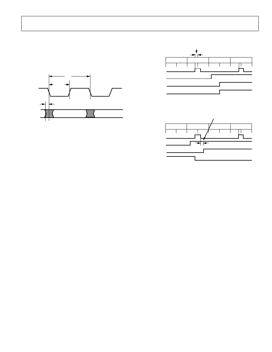
TIMING
The output data clock signal is created so that its rising edge
always occurs between data transitions and can be used to latch
the output data externally.
Figure 3 shows the timing operation of the AD9397.
t
PER
t
DCYCLE
t
SKEW
DATACK
05691-003
DATA
HSOUT
Figure 3. Output Timing
HSYNC TIMING
Horizontal sync (HSYNC) is processed in the AD9397 to
eliminate ambiguity in the timing of the leading edge with
respect to the phase-delayed pixel clock and data.
The HSYNC input is used as a reference to generate the pixel
sampling clock. The sampling phase can be adjusted, with
respect to HSYNC, through a full 360° in 32 steps via the phase
adjust register (to optimize the pixel sampling time). Display
systems use HSYNC to align memory and display write cycles,
so it is important to have a stable timing relationship between
the HSYNC output (HSOUT) and data clock (DATACK).
VSYNC FILTER AND ODD/EVEN FIELDS
The VSYNC filter is used to eliminate spurious VSYNCs,
maintain a consistent timing relationship between the VSYNC
and HSYNC output signals, and generate the odd/even field
output.
The filter works by examining the placement of VSYNC
with respect to HSYNC and, if necessary, slightly shifting
it in time at the VSOUT output. The goal is to keep the
VSYNC and HSYNC leading edges from switching at the
same time, eliminating confusion as to when the first line
of a frame occurs. Enabling the VSYNC filter is done with
Register 0x21[5]. Use of the VSYNC filter is recommended for
all cases, including interlaced video, and is required when using
the HSYNC per VSYNC counter. Figure 4 and Figure 5
illustrate even/odd field determination in two situations.
FIELD 1
FIELD 0
SYNC SEPARATOR THRESHOLD
FIELD 1
FIELD 0
2
3
2
1
4
4
3
1
HSIN
VSIN
VSOUT
O/E FIELD
EVEN FIELD
QUADRANT
05691-004
Figure 4. VSYNC Filter
FIELD 1
FIELD 0
SYNC SEPARATOR THRESHOLD
FIELD 1
FIELD 0
2
3
2
1
4
4
3
1
HSIN
VSIN
VSOUT
O/E FIELD
ODD FIELD
QUADRANT
05691-005
Figure 5. VSYNC Filter--Odd/Even
DVI RECEIVER
The DVI receiver section of the AD9397 allows the reception of
a digital video stream compatible with DVI 1.0. Embedded in
this data stream are HSYNCs, VSYNCs, and display enable
(DE) signals. DVI restricts the received format to RGB, but the
inclusion of a programmable color space converter (CSC)
allows the output to be tailored to any format necessary. With
this, the scaler following the AD9397 can specify that it always
wishes to receive a particular format--for instance, 4:2:2
YCrCb--regardless of the transmitted mode. If RGB is sent, the
CSC can easily convert that to 4:2:2 YCrCb while relieving the
scaler of this task.
DE GENERATOR
The AD9397 has an onboard generator for DE, for start of
active video (SAV), and for end of active video (EAV), all of
which are necessary for describing the complete data stream for
a BT656-compatible output. In addition to this particular
output, it is possible to generate the DE for cases in which a
scaler is not used. This signal alerts the following circuitry as to
which are displayable video pixels.
AD9397
Rev. 0 | Page 12 of 28
4:4:4 TO 4:2:2 FILTER
The AD9397 contains a filter that allows it to convert a signal
from YCrCb 4:4:4 to YCrCb 4:2:2 while maintaining the
maximum accuracy and fidelity of the original signal.
Input Color Space to Output Color Space
The AD9397 can support a wide variety of output formats,
such as:
·
RGB 24-bit
·
4:4:4 YCrCb 8-bit
·
4:2:2 YCrCb 8-bit, 10-bit, and 12-bit
·
Dual 4:2:2 YCrCb 8-bit
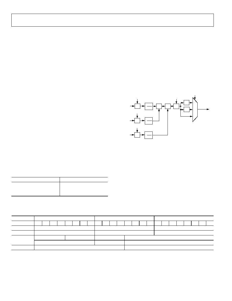
Color Space Conversion (CSC) Matrix
The CSC matrix in the AD9397 consists of three identical
processing channels. In each channel, three input values are
multiplied by three separate coefficients. Also included are an
offset value for each row of the matrix and a scaling multiple
for all values. Each value has a 13-bit, twos complement
resolution to ensure the signal integrity is maintained. The
CSC is designed to run at speeds up to 150 MHz supporting
resolutions up to 1080p at 60 Hz. With any-to-any color space
support, formats such as RGB, YUV, YCbCr, and others are
supported by the CSC.
The main inputs, R
IN
, G
IN
, and B
IN
, come from the 8-bit to 12-bit
inputs from each channel. These inputs are based on the input
format detailed in Table 9. The mapping of these inputs to the
CSC inputs is shown in Table 8.
Table 8. CSC Port Mapping
Input Channel
CSC Input Channel
R/CR R
IN
Gr/Y G
IN
B/CB B
B
IN
One of the three channels is represented in Figure 6. In each
processing channel, the three inputs are multiplied by three
separate coefficients marked a1, a2, and a3. These coefficients
are divided by 4096 to obtain nominal values ranging from
0.9998 to +0.9998. The variable labeled a4 is used as an offset
control. The CSC_Mode setting is the same for all three
processing channels. This multiplies all coefficients and offsets
by a factor of 2
CSC_Mode
.
The functional diagram for a single channel of the CSC, as
shown in Figure 6, is repeated for the remaining G and B
channels. The coefficients for these channels are b1, b2, b3, b4,
c1, c2, c3, and c4.
05691-
006
×2
2
1
0
×
×
×
a1[12:0]
a2[12:0]
a3[12:0]
R
IN
[11:0]
G
IN
[11:0]
B
IN
[11:0]
+
×4
CSC_Mode[1:0]
a4[12:0]
R
OUT
[11:0]
+
1
4096
×
1
4096
×
1
4096
×
+
Figure 6. Single CSC Channel
A programming example and register settings for several
common conversions are listed in the Color Space Converter
(CSC) Common Settings section.
For a detailed functional description and more programming
examples, refer to the Application Note
AN-795, AD9880 Color
Space Converter User's Guide.
OUTPUT DATA FORMATS
The AD9398 supports 4:4:4, 4:2:2, double data-rate (DDR), and
BT656 output formats. Register 0x25[3:0] controls the output
mode. These modes and the pin mapping are illustrated in
Table 8.
Table 9.
Port Red
Green
Blue
Bit
7 6 5 4 3 2 1 0 7 6 5 4 3 2 1 0 7 6 5 4 3 2 1 0
4:4:4
Red/Cr [7:0]
Green/Y [7:0]
Blue/Cb [7:0]
4:2:2
CbCr [7:0]
Y [7:0]
DDR 4:2:2
CbCr
Y, Y
DDR
1
G [3:0]
DDR
B [7:4]
DDR
B [3:0]
DDR 4:2:2
CbCr [11:0]
4:4:4 DDR
DDR
R [7:0]
DDR
G [7:4]
DDR 4:2:2
Y,Y [11:0]
4:2:2 to 12
CbCr[11:0]
Y [11:0]
1
Arrows in the table indicate clock edge. Rising edge of clock =
, falling edge = .
AD9397
Rev. 0 | Page 13 of 28
2-WIRE SERIAL REGISTER MAP
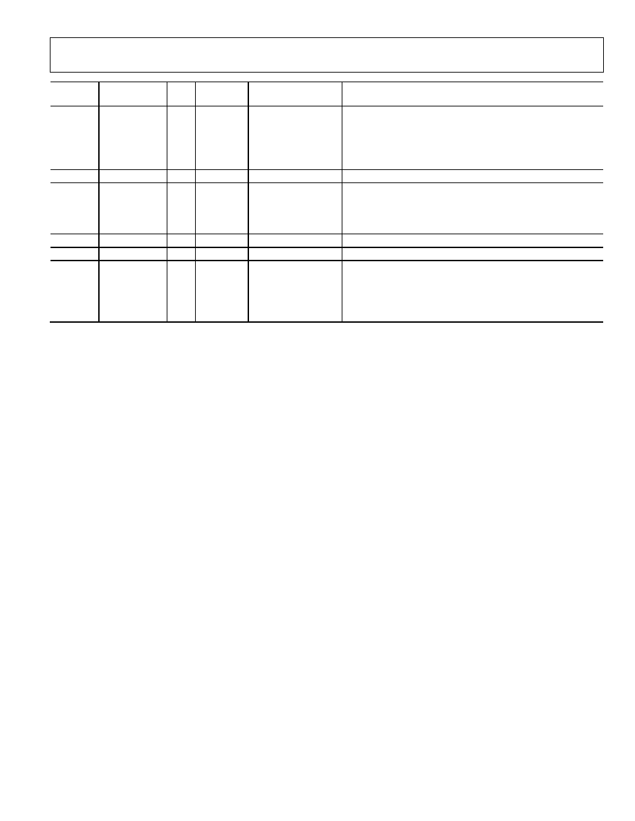
The AD9397 is initialized and controlled by a set of registers that determines the operating modes. An external controller is employed to
write and read the control registers through the 2-wire serial interface port.
Table 10. Control Register Map
Hex
Address
Read/Write
or Read Only
Bits
Default
Value
Register Name
Description
0x00
Read
[7:0]
00000000
Chip Revision
Chip revision ID.
0x11
Read/Write
[7]
0*******
HSYNC Source
0 = HSYNC.
1 = SOG.
[6]
*0******
HSYNC Source
Override
0 = auto HSYNC source.
1 = manual HSYNC source.
[5]
**0*****
VSYNC Source
0 = VSYNC.
1 = VSYNC from SOG.
[4]
***0****
VSYNC Source
Override
0 = auto HSYNC source.
1 = manual HSYNC source.
[3]
****0***
Channel Select
0 = Channel 0.
1 = Channel 1.
[2]
*****0**
Channel Select
Override
0 = autochannel select.
1 = manual channel select.
[1]
******0*
Interface Select
0 = analog interface.
1 = digital interface.
[0]
*******0
Interface Override
0 = auto-interface select.
1 = manual interface select.
0x12
Read/Write
[7]
1*******
Input HSYNC Polarity
0 = active low.
1 = active high.
[6]
*0******
HSYNC Polarity
Override
0 = auto HSYNC polarity.
1 = manual HSYNC polarity.
[5]
**1*****
Input VSYNC Polarity
0 = active low.
1 = active high.
[4]
***0****
VSYNC Polarity
Override
0 = auto VSYNC polarity.
1 = manual VSYNC polarity.
0x17 Read
[3:0]
****0000
HSYNCs per VSYNC
MSB
MSB of HSYNCs per VSYNC.
0x18
Read
[7:0]
00000000
HSYNCs per VSYNC
HSYNCs per VSYNC count.
0x22
Read/Write
[7:0]
4
VSYNC Duration
VSYNC duration.
0x23 Read/Write
[7:0]
32
HSYNC
Duration HSYNC duration. Sets the duration of the output HSYNC in pixel
clocks.
0x24 Read/Write
[7]
1*******
HSYNC Output
Polarity
Output HSYNC polarity.
0 = active low out.
1 = active high out.
[6]
*1******
VSYNC Output
Polarity
Output VSYNC polarity.
0 = active low out.
1 = active high out.
[5]
**1*****
DE Output Polarity
Output DE polarity.
0 = active low out.
1 = active high out.
AD9397
Rev. 0 | Page 14 of 28
Hex
Address
Read/Write
or Read Only
Bits
Default
Value Register
Name Description
[4]
**1****
ield Output Polarity
utput field polarity.
*
F
O
0 = active low out.
1 = active high out.
[0]
******0
utput CLK Invert
out.
*
O
0 = Don't invert clock
1 = Invert clock out.
0x25
Read/Write
:6]
1******
utput CLK Select
use on output pin. 1× CLK is divided
[7
0
O
Selects which clock to
down from TMDS clock input when pixel repetition is in use.
00 = ½× CLK.
01 = 1× CLK.
10 = 2× CLK.
11 = 90° phase 1× CLK.
[5:4]
*11****
utput Drive
f the outputs.
*
O
Strength
Sets the drive strength o
00 = lowest, 11 = highest.
[3:2]
***00**
utput Mode
comes out on.
*
O
Selects which pins the data
00 = 4:4:4 mode (normal).
01 = 4:2:2 + DDR 4:2:2 on blue.
10 = DDR 4:4:4 + DDR 4:2:2 on blue.
[1]
*****1*
rimary Output
*
P
Enable
Enables primary output.
[0]
*******0 ry Output
Enables secondary output (DDR 4:2:2 in Output Mode 1 and
Seconda
Enable
Mode 2).
0x26
Read/Write
[7]
0*******
ee-State
e the outputs.
Output Thr
Three-stat
[5]
**0*****
SPDIF Three-State
Three-state the SPDIF output.
[4]
***0****
I
2
S Three-State
Three-state the I
2
S output and the MCLK out.
[3]
****1***
Power-Down Pin
Polarity
Sets polarity of power-down pin.
0 = active low.
1 = active high.
[2:1]
****00*
ower-Down Pin
wer-down pin.
*
P
Function
Selects the function of the po
00 = power-down.
01 = power-down and three-state SOG.
10 = three-state outputs only.
11 = three-state outputs and SOG.
[0]
******0
ower-Down
*
P
0 = normal.
1 = power-down.
0x27 Read/Write ]
******* uto Power-Down
w power state.
[7
1
A
Enable
0 = disable auto lo
1 = enable auto low power state.
[6]
0******
DCP
A0
HDCP I
2
C. Set to 1 only for a
*
H
Sets the LSB of the address of the
second receiver in a dual-link configuration.
0 = use internally generated MCLK.
1 = use external MCLK input.
[5]
*0*****
CLK External
must be locked to the video clock
*
M
Enable
If an external MCLK is used, it
according to the CTS and N available in the I
2
C. Any mismatch
between the internal MCLK and the input MCLK results in
dropped or repeated audio samples.
[4]
***0****
BT656
EN
into the video output
Enables EAV/SAV codes to be inserted
data.
[3]
****0***
Force DE Generation
use of the internal DE generator in DVI mode.
Allows
[2:0]
n Field 0
*****000
Interlace
Offset
Sets the difference (in HSYNCs) in field length betwee
and Field 1.
AD9397
Rev. 0 | Page 15 of 28
Hex
Address
Read/Write
or Read Only
Bits
Default
Value Register
Name Description
0x28 Read/Write :2]
11000**
S
Delay
ets the delay (in lines) from the VSYNC leading edge to the start
[7
0
V
S
of active video.
[1:0]
******01
HS Delay MSB
29.
MSB, Register 0x
0x29 Read/Write
els) from the HSYNC leading edge to the
[7:0]
00000100
HS
Delay
Sets the delay (in pix
start of active video.
0x2A
Read/Write
[3:0]
****0101
Line Width MSB
MSB, Register 0x2B.
0x2B
Read/Write
[7:0]
00000000
Line Width
Sets the width of the active video line in pixels.
0x2C
Read/Write
[3:0]
****0010
Screen Height MSB
MSB, Register 0x2D.
0x2D
Read/Write
[7:0]
11010000
Screen Height
Sets the height of the active screen in lines.
0x2E
Read/Write
[7]
0*******
Test 1
Must be written to 1 for proper operation.
0x2F
Read
[6]
*0******
TMDS Sync Detect
Detects a TMDS DE.
[5]
**0*****
TMDS Active
Detects a TMDS clock.
[3]
****0***
HDCP Keys Read
EEPROM keys is successful.
Returns 1 when read of
[2:0]
*****000
DVI Quality
Returns quality number based on DE edges.
0x30 Read
se (content is
d.
ar
[6]
*0******
DVI Content
Encrypted
This bit is high when HDCP decryption is in u
protected). The signal goes low when HDCP is not being use
Customers can use this bit to determine whether to allow
copying of the content. The bit should be sampled at regul
intervals because it can change on a frame-by-frame basis.
[5]
**0*****
DVI HSYNC Polarity
Returns DVI HSYNC polarity.
[4]
***0****
DVI VSYNC Polarity
Returns DVI VSYNC polarity.
0x31
Read/Write
]
nc pulse width for Macrovision
[7:4
1001****
MV Pulse Max
Sets the maximum pseudo sy
detection.
[3:0]
****0110
MV Pulse Min
nimum pseudo sync pulse width for Macrovision®
Sets the mi
detection.
0x32 Read/Write
[7]
0*******
MV
Oversample
En
crovision detection engine whether we are
Tells the Ma
oversampling or not.
[6]
*0******
MV Pal En
etection engine to enter PAL mode.
Tells the Macrovision d
[5:0]
unt Start
**001101
MV Line Co
Sets the start line for Macrovision detection.
0x33
Read/Write
[7]
1*******
MV Detect Mode
0 = standard definition.
1 = progressive scan mode.
[6]
0******
V Settings Override
for line counts and pulse widths.
*
M
0 = use hard-coded settings
1 = use I
2
C values for these settings.
[5:0]
*010101
V Line Count End
ection.
*
M
Sets the end line for Macrovision det
0x34
Read/Write
t 3 lines (SD mode
[7:6]
10******
MV Pulse Limit Set
Sets the number of pulses required in the las
only).
[5]
**0*****
Low Freq Mode
dio PLL to low frequency mode. Low frequency mode
Sets au
should only be set for pixel clocks <80 MHz.
[4]
***0****
Low
Freq
Override
frequency mode
Allows the previous bit to be used to set low
rather than the internal auto-detect.
[3]
****0***
Up Conversion Mode
0 = repeat Cr and Cb values.
1 = interpolate Cr and Cb values.
[2]
****0**
rCb Filter Enable
output.
*
C
Enables the FIR filter for 4:2:2 CrCb
[1]
******0*
CSC_Enable Enables the color space converter (CSC). The default settings for
the CSC provide HDTV-to-RGB conversion.
ficients, including
Sets the fixed point position of the CSC coef
the A4, B4, and C4 offsets.
0x35
Read/Write
[6:5]
*01* ****
CSC_Mode
00 = ±1.0, -4096 to +4095.
01 =±2.0, -8192 to +8190.
1× = ±4.0, -16384 to +16380.
[4:0]
**01100
SC_Coeff_A1 MSB
*
C
MSB, Register 0x36.
AD9397
Rev. 0 | Page 16 of 28
Hex
Address
Read/Write
or Read Only
Bits
Default
Value Register
Name Description
0x36
Read/Write
:0]
1010010
SC_Coeff_A1 LSB
olor space converter (CSC) coefficient for equation:
[7
0
C
C
R
OUT
= (A1 × R
IN
) + (A2 × G
IN
) + (A3 × B
IN
) + A4
G
OUT
= (B1 × R
IN
) + (B2 × G
IN
) + (B3 × B
IN
) + B4
B
B
OUT
= (C1 × R
IN
) + (C2 × G
IN
) + (C3 × B
IN
) + C4
0x37
Read/Write
:0]
**01000
SC_Coeff_A2 MSB
[4
*
C
MSB, Register 0x38.
0x38
Read/Write
[7:0]
00000000
CSC_Coeff_A2 LSB
CSC coefficient for equation:
R
OUT
= (A1 × R
IN
+ (A2 × G
IN
) + (A3 × B
IN
) + A4
G
OUT
= (B1 × R
IN
) + (B2 × G
IN
) + (B3 × B
IN
) + B4
B
B
OUT
= (C1 × R
IN
) + (C2 × G
IN
) + (C3 × B
IN
) + C4
0x39
Read/Write
:0]
**00000
SC_Coeff_A3 MSB
[4
*
C
MSB, Register 0x3A.
0x3A
Read/Write
[7:0]
00000000
CSC_Coeff_A3 LSB
CSC coefficient for equation:
R
OUT
= (A1 × R
IN
) + (A2 × G
IN
) + (A3 × B
IN
) + A4
G
OUT
= (B1 × R
IN
) + (B2 × G
IN
) + (B3 × B
IN
) + B4
B
B
OUT
= (C1 × R
IN
) + (C2 × G
IN
) + (C3 × B
IN
) + C4
0x3B
Read/Write
:0]
**11001
SC_Coeff_A4 MSB
[4
*
C
MSB, Register 0x3C.
0x3C
Read/Write
[7:0]
11010111
CSC_Coeff_A4 LSB
CSC coefficient for equation:
R
OUT
= (A1 × R
IN
) + (A2 × G
IN
) + (A3 × B
IN
) + A4
G
OUT
= (B1 × R
IN
) + (B2 × G
IN
) + (B3 × B
IN
) + B4
B
B
OUT
= (C1 × R
IN
) + (C2 × G
IN
) + (C3 × B
IN
) + C4
0x3D
Read/Write
:0]
**11100
SC_Coeff_B1 MSB
[4
*
C
MSB, Register 0x3E.
0x3E
Read/Write
[7:0]
01010100
CSC_Coeff_B1 LSB
CSC coefficient for equation:
R
OUT
= (A1 × R
IN
) + (A2 × G
IN
) + (A3 × B
IN
) + A4
G
OUT
= (B1 × R
IN
) + (B2 × G
IN
) + (B3 × B
IN
) + B4
B
B
OUT
= (C1 × R
IN
) + (C2 × G
IN
) + (C3 × B
IN
) + C4
0x3F
Read/Write
:0]
**01000
SC_Coeff_B2 MSB
[4
*
C
MSB, Register 0x40.
0x40
Read/Write
[7:0]
00000000
CSC_Coeff_B2 LSB
CSC coefficient for equation:
R
OUT
= (A1 × R
IN
) + (A2 × G
IN
) + (A3 × B
IN
) + A4
G
OUT
= (B1 × R
IN
) + (B2 × G
IN
) + (B3 × B
IN
) + B4
B
B
OUT
= (C1 × R
IN
) + (C2 × G
IN
) + (C3 × B
IN
) + C4
0x41
Read/Write
:0]
**11110
SC_Coeff_B3 MSB
[4
*
C
MSB, Register 0x42.
0x42
Read/Write
[7:0]
10001001
CSC_Coeff_B3
CSC coefficient for equation:
R
OUT
= (A1 × R
IN
+ (A2 × G
IN
) + (A3 × B
IN
) + A4
G
OUT
= (B1 × R
IN
) + (B2 × G
IN
) + (B3 × B
IN
) + B4
B
B
OUT
= (C1 × R
IN
) + (C2 × G
IN
) + (C3 × B
IN
) + C4
0x43
Read/Write
:0]
**00010
SC_Coeff_B4 MSB
[4
*
C
MSB, Register 0x44.
0x44
Read/Write
[7:0]
10010010
CSC_Coeff_B4 LSB
CSC coefficient for equation:
R
OUT
= (A1 × R
IN
) + (A2 × R
IN
) + (A3 × B
IN
) + A4
G
OUT
= (B1 × R
IN
) + (B2 × G
IN
) + (B3 × B
IN
) + B4
B
B
OUT
= (C1 × R
IN
) + (C2 × G
IN
) + (C3 × B
IN
) + C4
0x45
Read/Write
:0]
**00000
SC_Coeff_C1 MSB
[4
*
C
MSB, Register 0x46.
0x46
Read/Write
[7:0]
00000000
CSC_Coeff_C1 LSB
CSC coefficient for equation:
R
OUT
= (A1 × R
IN
) + (A2 × G
IN
) + (A3 × B
IN
) + A4
G
OUT
= (B1 × R
IN
) + (B2 × G
IN
) + (B3 × B
IN
) + B4
B
B
OUT
= (C1 × R
IN
) + (C2 × G
IN
) + (C3 × B
IN
) + C4
0x47
Read/Write
:0]
**01000
SC_Coeff_C2 MSB
[4
*
C
MSB, Register 0x48.
0x48
Read/Write
[7:0]
00000000
CSC_Coeff_C2 LSB
CSC coefficient for equation:
R
OUT
= (A1 × R
IN
) + (A2 × G
IN
) + (A3 × B
IN
) + A4
G
OUT
= (B1 × R
IN
) + (B2 × G
IN
) + (B3 × B
IN
) + B4
B
B
OUT
= (C1 × R
IN
) + (C2 × G
IN
) + (C3 × B
IN
) + C4
AD9397
Rev. 0 | Page 17 of 28
Hex
Address
Read/Write
or Read Only
Bits
Default
Value Register
Name Description
0x49
Read/Write
[4:0]
***01110
CSC_Coeff_C3 MSB
MSB, Register 0x4A.
0x4A
Read/Write
[7:0]
10000111
CSC_Coeff_C3 LSB
CSC coefficient for equation:
R
OUT
= (A1 × R
IN
) + (A2 × G
IN
) + (A3 × B
IN
) + A4
G
OUT
= (B1 × R
IN
) + (B2 × G
IN
) + (B3 × B
IN
) + B4
B
B
OUT
= (C1 × R
IN
) + (C2 × G
IN
) + (C3 × B
IN
) + C4
0x4B
Read/Write
[4:0]
***11000
CSC_Coeff_C4 MSB
MSB, Register 0x4C.
0x4C
Read/Write
[7:0]
10111101
CSC_Coeff_C4 LSB
CSC coefficient for equation:
R
OUT
= (A1 × R
IN
) + (A2 × G
IN
) + (A3 × B
IN
) + A4
G
OUT
= (B1 × R
IN
) + (B2 × G
IN
) + (B3 × B
IN
) + B4
B
B
OUT
= (C1 × R
IN
) + (C2 × G
IN
) + (C3 × B
IN
) + C4
0x50
Read/Write
[7:0]
00100000
Test
Must be written to 0x20 for proper operation.
0x56
Read/Write
[7:0]
00001111
Test
Must be written to default of 0x0F for proper operation.
0x59
Read/Write
[6]
MDA/MCL PU
This disables the MDA/MCL pull-ups.
[5]
CLK Term O/R
Clock termination power-down override: 0 = auto, 1 = manual.
[4]
Manual CLK Term
Clock termination: 0 = normal, 1 = disconnected.
[0]
MDA/MCL Three-
State
This bit three-states the MDA/MCL lines.

AD9397
Rev. 0 | Page 18 of 28
2-WIRE SERIAL CONTROL REGISTER DETAILS
CHIP IDENTIFICATION
0x00--Bit[7:0] Chip Revision
An 8-bit value that reflects the current chip revision.
0x11--Bit[7] HSYNC Source
0 = HSYNC, 1 = SOG. The power-up default is 0. These
selections are ignored if Register 0x11, Bit 6 = 0.
0x11--Bit[6] HSYNC Source Override
0 = auto HSYNC source, 1 = manual HSYNC source. Manual
HSYNC source is defined in Register 0x11, Bit 7. The power-up
default is 0.
0x11--Bit[5] VSYNC Source
0 = VSYNC, 1 = VSYNC from SOG. The power-up default is 0.
These selections are ignored if Register 0x11, Bit 4 = 0.
0x11--Bit[4] VSYNC Source Override
0 = auto VSYNC source, 1 = manual VSYNC source. Manual
VSYNC source is defined in Register 0x11, Bit 5. The power-up
default is 0.
0x11--Bit[3] Channel Select
0 = Channel 0, 1 = Channel 1. The power-up default is 0. These
selections are ignored if Register 0x11, Bit 2 = 0.
0x11--Bit[2] Channel Select Override
0 = auto channel select, 1 = manual channel select. Manual
channel select is defined in Register 0x11, Bit 3. The power-up
default is 0.
0x11--Bit[1] Interface Select
0 = analog interface, 1 = digital interface. The power-up default
is 0. These selections are ignored if Register 0x11, Bit 0 = 0.
0x11--Bit[0] Interface Select Override
0 = auto interface select, 1 = manual interface select. Manual
interface select is defined in Register 0x11, Bit 1. The power-up
default is 0.
0x12--Bit[7] Input HSYNC Polarity
0 = active low, 1 = active high. The power-up default is 1. These
selections are ignored if Register 10x2, Bit 6 = 0.
0x12--Bit[6] HSYNC Polarity Override
0 = auto HSYNC polarity, 1 = manual HSYNC polarity. Manual
HSYNC polarity is defined in Register 0x11, Bit 7. The power-
up default is 0.
0x12--Bit[5] Input VSYNC Polarity
0 = active low, 1 = active high. The power-up default is 1. These
selections are ignored if Register 0x11, Bit 4 = 0.
0x12--Bit[4] VSYNC Polarity Override
0 = auto VSYNC polarity, 1 = manual VSYNC polarity. Manual
VSYNC polarity is defined in Register 0x11, Bit 5. The power-
up default is 0.
0x17--Bits[3:0] HSYNCs per VSYNC MSBs
The 4 MSBs of the 12-bit counter that reports the number of
HSYNCs/VSYNC on the active input. This is useful in
determining the mode and aids in setting the PLL divide ratio.
0x18--Bit[7:0] HSYNCs per VSYNC LSBs
The 8 LSBs of the 12-bit counter that reports the number of
HSYNCs/VSYNC on the active input.
0x21--Bit[5] VSYNC Filter Enable
The purpose of the VSYNC filter is to guarantee the position of
the VSYNC edge with respect to the HSYNC edge and to
generate a field signal. The filter works by examining the
placement of VSYNC and regenerating a correctly placed
VSYNC one line later. The VSYNC is first checked to see
whether it occurs in the Field 0 position or the Field 1 position.
This is done by checking the leading edge position against the
sync separator threshold and the HSYNC position. The HSYNC
width is divided into four quadrants with Quadrant 1 starting at
the HSYNC leading edge plus a sync separator threshold. If the
VSYNC leading edge occurs in Quadrant 1 or Quadrant 4, the
field is set to 0 and the output VSYNC is placed coincident with
the HSYNC leading edge. If the VSYNC leading edge occurs in
Quadrant 2 or Quadrant 3, the field is set to 1 and the output
VSYNC leading edge is placed in the center of the line. In this
way, the VSYNC filter creates a predictable relative position
between HSYNC and VSYNC edges at the output.
If the VSYNC occurs near the HSYNC edge, this guarantees
that the VSYNC edge follows the HSYNC edge. This performs
filtering also in that it requires a minimum of 64 lines between
VSYNCs. The VSYNC filter cleans up extraneous pulses that
might occur on the VSYNC. This should be enabled whenever
the HSYNC/VSYNC count is used. Setting this bit to 0 disables
the VSYNC filter. Setting this bit to 1 enables the VSYNC filter.
Power-up default is 0.
0x21--Bit[4] VSYNC Duration Enable
This enables the VSYNC duration block which is designed to
be used with the VSYNC filter. Setting the bit to 0 leaves the
VSYNC output duration unchanged; setting the bit to 1 sets the
VSYNC output duration based on Register 0x22. The power-up
default is 0.
0x22--Bits[7:0] VSYNC Duration
This is used to set the output duration of the VSYNC, and is
designed to be used with the VSYNC filter. This is valid only if
Register 0x21, Bit 4 is set to 1. Power-up default is 4.
AD9397
Rev. 0 | Page 19 of 28
0x23--Bit[7:0] HSYNC Duration
An 8-bit register that sets the duration of the HSYNC output
pulse. The leading edge of the HSYNC output is triggered by
the internally generated, phase-adjusted PLL feedback clock.
The AD9397 then counts a number of pixel clocks equal to the
value in this register. This triggers the trailing edge of the
HSYNC output, which is also phase-adjusted. The power-up
default is 32.
0x24--Bit[7] HSYNC Output Polarity
This bit sets the polarity of the HSYNC output. Setting this bit
to 0 sets the HSYNC output to active low. Setting this bit to 1
sets the HSYNC output to active high. Power-up default setting
is 1.
0x24--Bit[6] VSYNC Output Polarity
This bit sets the polarity of the VSYNC output (both DVI and
analog). Setting this bit to 0 sets the VSYNC output to active
low. Setting this bit to 1 sets the VSYNC output to active high.
Power-up default is 1.
0x24--Bit[5] Display Enable Output Polarity
This bit sets the polarity of the display enable (DE) for both
DVI and analog. 0 = DE output polarity is negative. 1 = DE
output polarity is positive. The power-up default is 1.
0x24--Bit[4] Field Output Polarity
This bit sets the polarity of the field output signal (both DVI
and analog) on Pin 21. 0 = active low out = even field; active
high = odd field. 1 = active high out = odd field; active high =
even field. The power-up default is 1.
0x24--Bit[0] Output Clock Invert
This bit allows inversion of the output clock as specified by
Register 0x25, Bits 7 to 6. 0 = noninverted clock. 1 = inverted
clock. The power-up default setting is 0.
0x25--Bits[7:6] Output Clock Select
These bits select the clock output on the DATACLK pin. They
include 1/2× clock, a 2× clock, a 90° phase shifted clock, or the
normal pixel clock. The power-up default setting is 01.
Table 11. Output Clock Select
Select Result
00
½× pixel clock
01
1× pixel clock
10
2× pixel clock
11
90° phase 1× pixel clock
0x25--Bit[5:4] Output Drive Strength
These two bits select the drive strength for all the high speed
digital outputs (except VSOUT, A0 and O/E field). Higher drive
strength results in faster rise/fall times and in general makes it
easier to capture data. Lower drive strength results in slower
rise/fall times and helps to reduce EMI and digitally generated
power supply noise. The power-up default setting is 11.
Table 12. Output Drive Strength
Output Drive
Result
00
Low output drive strength
01
Medium low output drive strength
10
Medium high output drive strength
11
High output drive strength
0x25--Bits[3:2] Output Mode
These bits choose between four options for the output mode,
one of which is exclusive to an HDMI input. 4:4:4 mode is
standard RGB; 4:2:2 mode is YCrCb, which reduces the number
of active output pins from 24 to 16; 4:4:4 is double data rate
(DDR) output mode; and the data is RGB mode, but changes on
every clock edge. The power-up default setting is 00.
Table 13. Output Mode
Output Mode
Result
00
4:4:4 RGB mode
01
4:2:2 YCrCb mode + DDR 4:2:2 on blue
(secondary)
10
DDR 4:4:4: DDR mode + DDR 4:2:2 on blue
(secondary)
11
12-bit 4:2:2 (HDMI option only)
0x25--Bit[1] Primary Output Enable
This bit places the primary output in active or high impedance
mode. The primary output is designated when using either 4:2:2
or DDR 4:4:4. In these modes, the data on the red and green
output channels is the primary output, while the output data
on the blue channel (DDR YCrCb) is the secondary output.
0 = primary output is in high impedance mode. 1 = primary
output is enabled. The power-up default setting is 1.
0x25--Bit[0] Secondary Output Enable
This bit places the secondary output in active or high
impedance mode. The secondary output is designated when
using either 4:2:2 or DDR 4:4:4. In these modes, the data on
the blue output channel is the secondary output while the
output data on the red and green channels is the primary
output. Secondary output is always a DDR YCrCb data mode.
The power-up default setting is 0. 0 = secondary output is in
high impedance mode. 1 = secondary output is enabled.

AD9397
Rev. 0 | Page 20 of 28
0x26--Bit[7] Output Three-State
When enabled, this bit puts all outputs (except SOGOUT) in a
high impedance state. 0 = normal outputs. 1 = all outputs
(except SOGOUT) in high impedance mode. The power-up
default setting is 0.
0x26--Bit[3] Power-Down Polarity
This bit defines the polarity of the input power-down pin. 0 =
power-down pin is active low. 1 = power-down pin is active
high. The power-up default setting is 1.
0x26--Bits[2:1] Power-Down Pin Function
These bits define the different operational modes of the power-
down pin. These bits are functional only when the power-down
pin is active; when it is not active, the part is powered up and
functioning. 0x = the chip is powered down and all outputs are
in high impedance mode. 1x = the chip remains powered up,
but all outputs are in high impedance mode. The power-up
default setting is 00.
0x26--Bit[0] Power-Down
This bit is used to put the chip in power-down mode. In this
mode, the power dissipation is reduced to a fraction of the
typical power (see Table 1 for exact power dissipation). When in
power-down, the HSOUT, VSOUT, DATACK, and all 30 of the
data outputs are put into a high impedance state. Note that the
SOGOUT output is not put into high impedance. Circuit blocks
that continue to be active during power-down include the
voltage references, sync processing, sync detection, and the
serial register. These blocks facilitate a fast start-up from power-
down. 0 = normal operation. 1 = power-down. The power-up
default setting is 0.
0x27--Bit[7] Auto Power-Down Enable
This bit enables the chip to go into low power mode, or seek
mode if no sync inputs are detected. 0 = auto power-down
disabled. 1 = chip powers down if no sync inputs present. The
power-up default setting is 1.
0x27--Bit[6] HDCP A0 Address
This bit sets the LSB of the address of the HDCP I
2
C. This
should be set to 1 only for a second receiver in a dual-link
configuration. The power-up default is 0.
BT656 GENERATION
0x27--Bit[4] BT656 Enable
This bit enables the output to be BT656 compatible with the
defined start of active video (SAV) and end of active video
(EAV) controls to be inserted. These require specification of the
number of active lines, active pixels per line, and delays to place
these markers. 0 = disable BT656 video mode. 1 = enable BT656
video mode. The power-up default setting is 0.
0x27--Bit[3] Force DE Generation
This bit allows the use of the internal DE generator in DVI
mode. 0 = internal DE generation disabled. 1 = force DE
generation via programmed registers. The power-up default
setting is 0.
0x27--Bits[2:0] Interlace Offset
These bits define the offset in HSYNCs from Field 0 to Field 1.
The power-up default setting is 000.
0x28--Bits[7:2] VSYNC Delay
These bits set the delay (in lines) from the leading edge of
VSYNC to active video. The power-up default setting is 24.
0x28--Bit[1:0] HSYNC Delay MSBs
These 2 bits and the following 8 bits set the delay (in pixels)
from the HSYNC leading edge to the start of active video. The
power-up default setting is 0x104.
0x29--Bits[7:0] HSYNC Delay LSBs
See the HSYNC Delay MSBs section.
0x2A--Bits[3:0] Line Width MSBs
These 4 bits and the following 8 bits set the width of the active
video line (in pixels). The power-up default setting is 0x500.
0x2B--Bits[7:0] Line Width LSBs
See the line width MSBs section.
0x2C--Bits[3:0] Screen Height MSBs
These 4 bits and the following 8 bits set the height of the active
screen (in lines). The power-up default setting is 0x2D0.
0x2D--Bits[7:0] Screen Height LSBs
See the Screen Height MSBs section.
0x2F--Bit[6] TMDS Sync Detect
This read-only bit indicates the presence of a TMDS DE. 0 = no
TMDS DE present. 1 = TMDS DE detected.
0x2F--Bit[5] TMDS Active
This read-only bit indicates the presence of a TMDS clock. 0 =
no TMDS clock present. 1 = TMDS clock detected.
0x2F--Bit[3] HDCP Keys Read
This read-only bit reports if the HDCP keys were read
successfully. 0 = failure to read HDCP keys. 1 = HDCP keys
read.
0x2F--Bits[2:0] DVI Quality
These read-only bits indicate a level of DVI quality based on the
DE edges. A larger number indicates a higher quality.

AD9397
Rev. 0 | Page 21 of 28
0x30--Bit[6] DVI Content Encrypted
This read-only bit is high when HDCP decryption is in use
(content is protected). The signal goes low when HDCP is not
being used. Customers can use this bit to allow copying of the
content. The bit should be sampled at regular intervals because
it can change on a frame-by-frame basis. 0 = HDCP not in use.
1 = HDCP decryption in use.
0x30--Bit[5] DVI HSYNC Polarity
This read-only bit indicates the polarity of the DVI HSYNC. 0 =
DVI HSYNC polarity is low active. 1 = DVI HSYNC polarity is
high active.
0x30--Bit[4] DVI VSYNC Polarity
This read-only bit indicates the polarity of the DVI VSYNC.
0 = DVI VSYNC polarity is low active. 1 = DVI VSYNC polarity
is high active.
MACROVISION
0x31--Bits[7:4] Macrovision Pulse Max
These bits set the pseudo sync pulse width maximum for
Macrovision detection in pixel clocks. This is functional for
13.5 MHz SDTV or 27 MHz progressive scan. Power-up
default is 9.
0x31--Bits[3:0] Macrovision Pulse Min
These bits set the pseudo sync pulse width maximum for
Macrovision detection in pixel clocks. This is functional for
13.5 MHz SDTV or 27 MHz progressive scan. Power up
default is 6.
0x32--Bit[7] Macrovision Oversample Enable
Tells the Macrovision detection engine whether oversampling
is used. This accommodates 27 MHz sampling for SDTV and
54 MHz sampling for progressive scan and is used as a
correction factor for clock counts. Power-up default is 0.
0x32--Bit[6] Macrovision PAL Enable
Tells the Macrovision detection engine to enter PAL mode when
set to 1. Default is 0 for NTSC mode.
0x32--Bits[5:0] Macrovision Line Count Start
Set the start line for Macrovision detection. Along with
Register 0x33, Bits [5:0], they define the region where MV
pulses are expected to occur. The power-up default is Line 13.
0x33--Bit[7] Macrovision Detect Mode
0 = standard definition. 1 = progressive scan mode
0x33--Bit[6] Macrovision Settings Override
This defines whether preset values are used for the MV line
counts and pulse widths or the values stored in I
2
C registers are
used. 0 = use hard-coded settings for line counts and pulse
widths. 1 = use I
2
C values for these settings.
0x33--Bits[5:0] Macrovision Line Count End
Set the end line for Macrovision detection. Along with Register
0x32, Bits [5:0], they define the region where MV pulses are
expected to occur. The power-up default is Line 21.
0x34--Bits[7:6] Macrovision Pulse Limit Select
Set the number of pulses required in the last three lines (SD
mode only). If there is not at least this number of MV pulses,
the engine stops. These two bits define these pulse counts:
00 = 6.
01 = 4.
10 = 5 (default).
11 = 7.
0x34--Bit[5] Low Frequency Mode
Sets whether the audio PLL is in low frequency mode or not.
Low frequency mode should only be set for pixel clocks
<80 MHz.
0x34--Bit[4] Low Frequency Override
Allows the previous bit to be used to set low frequency mode
rather than the internal autodetect.
0x34--Bit[3] Upconversion Mode
0 = repeat Cb/Cr values. 1 = interpolate Cb/Cr values.
0x34--Bit[2] CbCr Filter Enable
Enables the FIR filter for 4:2:2 CbCr output.
COLOR SPACE CONVERSION
The default power-up values for the color space converter
coefficients (R0x35 through R0x4C) are set for ATSC RGB-to-
YCbCr conversion. They are completely programmable for
other conversions.
0x34--Bit[1] Color Space Converter Enable
This bit enables the color space converter. 0 = disable color
space converter. 1 = enable color space converter. The power-up
default setting is 0.
0x35--Bits[6:5] Color Space Converter Mode
These two bits set the fixed-point position of the CSC
coefficients, including the A4, B4, and C4 offsets. Default = 01.
Table 14. CSC Fixed Point Converter Mode
Select Result
00
±1.0, -4096 to +4095
01
±2.0, -8192 to +8190
1×
±4.0, -16384 to +16380

AD9397
Rev. 0 | Page 22 of 28
0x35--Bits[4:0] Color Space Conversion Coefficient A1 MSBs
These 5 bits form the 5 MSBs of the Color Space Conversion
Coefficient A1. This combined with the 8 LSBs of the following
register form a 13-bit, twos complement coefficient which is
user programmable. The equation takes the form of:
R
OUT
= (A1 × R
IN
) + (A2 × G
IN
) + (A3 × B
IN
) + A4
G
OUT
= (B1 × R
IN
) + (B2 × G
IN
) + (B3 × B
IN
) + B4
B
OUT
= (C1 × R
IN
) + (C2 × G
IN
) + (C3 × B
IN
) + C4
The default value for the 13-bit A1 coefficient is 0x0C52.
0x36--Bits[7:0] Color Space Conversion Coefficient A1 LSBs
See the Register 0x35 section.
0x37--Bits[4:0] CSC A2 MSBs
These five bits form the 5 MSBs of the Color Space Conversion
Coefficient A2. Combined with the 8 LSBs of the following
register they form a 13-bit, twos complement coefficient that is
user programmable. The equation takes the form of:
R
OUT
= (A1 × R
IN
) + (A2 × G
IN
) + (A3 × B
IN
) + A4
G
OUT
= (B1 × R
IN
) + (B2 × G
IN
) + (B3 × B
IN
) + B4
B
OUT
= (C1 × R
IN
) + (C2 × G
IN
) + (C3 × B
IN
) + C4
The default value for the 13-bit A2 coefficient is 0x0800.
0x38--Bits[7:0] CSC A2 LSBs
See the Register 0x37 section.
0x39--Bits[4:0] CSC A3 MSBs
The default value for the 13-bit A3 is 0x0000.
0x3A--Bits[7:0] CSC A3 LSBs
0x3B--Bits[4:0] CSC A4 MSBs
The default value for the 13-bit A4 is 0x19D7.
0x3C--Bits[7:0] CSC A4 LSBs
0x3D--Bits[4:0] CSC B1 MSBs
The default value for the 13-bit B1 is 0x1C54.
0x3E--Bits[7:0] CSC B1 LSBs
0x3F--Bits[4:0] CSC B2 MSBs
The default value for the 13-bit B2 is 0x0800.
0x40--Bits[7:0] CSC B2 LSBs
0x41--Bits[4:0] CSC B3 MSBs
The default value for the 13-bit B3 is 0x1E89.
0x42--Bit[7:0] CSC B3 LSBs
0x43--Bit[4:0] CSC B4 MSBs
The default value for the 13-bit B4 is 0x0291.
0x44--Bits[7:0] CSC B4 LSBs
0x45--Bits[4:0] CSC C1 MSBs
The default value for the 13-bit C1 is 0x0000.
0x46--Bits[7:0] CSC C1 LSBs
0x47--Bits[4:0] CSC C2 MSBs
The default value for the 13-bit C2 is 0x0800.
0x48--Bits[7:0] CSC C2 LSBs
0x49--Bits[4:0] CSC C3 MSBs
The default value for the 13-bit C3 is 0x0E87.
0x4A--Bits[7:0] CSC C3 LSBs
0x4B--Bits[4:0] CSC C4 MSBs
The default value for the 13-bit C4 is 0x18BD.
0x4C--Bits[7:0] CSC C4 LSBs
0x59--Bit[6] MDA/MCL PU Disable
This bit disables the inter-MDA/MCL pull-ups.
0x59--Bit[5] CLK Term O/R
This bit allows for overriding during power down.
0 = auto, 1 = manual.
0x59--Bit[4] Manual CLK Term
This bit allows normal clock termination or disconnects this. 0
= normal, 1 = disconnected.
0x59--Bit[0] MDA/MCL Three-State
This bit three-states the MDA/MCL lines to allow in-circuit
programming of the EEPROM.
AD9397
Rev. 0 | Page 23 of 28
2-WIRE SERIAL CONTROL PORT
DATA TRANSFER VIA SERIAL INTERFACE
For each byte of data read or written, the MSB is the first bit of
the sequence.
A 2-wire serial interface control interface is provided in the
AD9397. Up to two AD9397 devices can be connected to the
2-wire serial interface, with a unique address for each device.
If the AD9397 does not acknowledge the master device during a
write sequence, the SDA remains high so the master can gener-
ate a stop signal. If the master device does not acknowledge the
AD9397 during a read sequence, the AD9397 interprets this as
the end of data. The SDA remains high, so the master can
generate a stop signal.
The 2-wire serial interface comprises a clock (SCL) and a
bidirectional data (SDA) pin. The analog flat panel interface
acts as a slave for receiving and transmitting data over the serial
interface. When the serial interface is not active, the logic levels
on SCL and SDA are pulled high by external pull-up resistors.
To write data to specific control registers of the AD9397, the
8-bit address of the control register of interest must be written
after the slave address has been established. This control register
address is the base address for subsequent write operations. The
base address auto-increments by 1 for each byte of data written
after the data byte intended for the base address. If more bytes
are transferred than there are available addresses, the address
does not increment and remains at its maximum value. Any
base address higher than the maximum value does not produce
an acknowledge signal.
Data received or transmitted on the SDA line must be stable for
the duration of the positive-going SCL pulse. Data on SDA must
change only when SCL is low. If SDA changes state while SCL is
high, the serial interface interprets that action as a start or stop
sequence.
There are six components to serial bus operation:
·
Start signal
·
Slave address byte
·
Base register address byte
·
Data byte to read or write
Data are read from the control registers of the AD9397 in a
similar manner. Reading requires two data transfer operations:
·
Stop signal
·
The base address must be written with the R/W bit of the
slave address byte low to set up a sequential read
operation.
·
Acknowledge (Ack)
When the serial interface is inactive (SCL and SDA are high),
communications are initiated by sending a start signal. The start
signal is a high-to-low transition on SDA while SCL is high.
This signal alerts all slave devices that a data transfer sequence
is coming.
·
Reading (the R/W bit of the slave address byte high) begins
at the previously established base address. The address of
the read register auto-increments after each byte is
transferred.
The first 8 bits of data transferred after a start signal comprise a
7-bit slave address (the first 7 bits) and a single R/W bit (the
eighth bit). The R/W bit indicates the direction of data transfer,
read from (1) or write to (0) the slave device. If the transmitted
slave address matches the address of the device (set by the state
of the SA0 input pin as shown in Table 15), the AD9397
acknowledges by bringing SDA low on the 9th SCL pulse. If the
addresses do not match, the AD9397 does not acknowledge.
To terminate a read/write sequence to the AD9397, a stop signal
must be sent. A stop signal comprises a low-to-high transition
of SDA while SCL is high.
A repeated start signal occurs when the master device driving
the serial interface generates a start signal without first genera-
ting a stop signal to terminate the current communication. This
is used to change the mode of communication (read, write)
between the slave and master without releasing the serial
interface lines.
Table 15. Serial Port Addresses
Bit 7
Bit 6
Bit 5
Bit 4
Bit 3
Bit 2
Bit 1
A
6
(MSB)
A
5
A
4
A
3
A
2
A
1
A
0
1
0 0 1 1 0 0
SDA
SCL
t
BUFF
t
STAH
t
DHO
t
DSU
t
DAL
t
DAH
t
STASU
t
STOSU
05691-007
Figure 7. Serial Port Read/Write Timing
AD9397
Rev. 0 | Page 24 of 28
SERIAL INTERFACE READ/WRITE EXAMPLES
Write to one control register:
·
Start signal
·
Slave address byte (R/W bit = low)
·
Base address byte
·
Data byte to base address
·
Stop signal
Write to four consecutive control registers:
·
Start signal
·
Slave address byte (R/W bit = low)
·
Base address byte
·
Data byte to base address
·
Data byte to (base address + 1)
·
Data byte to (base address + 2)
·
Data byte to (base address + 3)
·
Stop signal
Read from one control register:
·
Start signal
·
Slave address byte (R/W bit = low)
·
Base address byte
·
Start signal
·
Slave address byte (R/W bit = high)
·
Data byte from base address
·
Stop signal
Read from four consecutive control registers:
·
Start signal
·
Slave address byte (R/W bit = low)
·
Base address byte
·
Start signal
·
Slave address byte (R/W bit = high)
·
Data byte from base address
·
Data byte from (base address + 1)
·
Data byte from (base address + 2)
·
Data byte from (base address + 3)
·
Stop signal
BIT 7
ACK
BIT 6
BIT 5
BIT 4
BIT 3
BIT 2
BIT 1
BIT 0
SDA
SCL
05691-008
Figure 8. Serial Interface--Typical Byte Transfer

AD9397
Rev. 0 | Page 25 of 28
PCB LAYOUT RECOMMENDATIONS
The AD9397 is a high precision, high speed digital device. To
achieve the maximum performance from the part, it is impor-
tant to have a well laid-out board. The following is a guide for
designing a board using the AD9397.
POWER SUPPLY BYPASSING
It is recommended to bypass each power supply pin with a
0.1 F capacitor. The exception is in the case where two or more
supply pins are adjacent to each other. For these groupings of
powers/grounds, it is only necessary to have one bypass
capacitor. The fundamental idea is to have a bypass capacitor
within about 0.5 cm of each power pin. Also, avoid placing the
capacitor on the opposite side of the PC board from the
AD9397, because that interposes resistive vias in the path.
The bypass capacitors should be physically located between the
power plane and the power pin. Current should flow from the
power plane to the capacitor to the power pin. Do not make the
power connection between the capacitor and the power pin.
Placing a via underneath the capacitor pads down to the power
plane is generally the best approach.
It is particularly important to maintain low noise and good
stability of PV
DD
(the clock generator supply). Abrupt changes
in PV
DD
can result in similarly abrupt changes in sampling clock
phase and frequency. This can be avoided by careful attention to
regulation, filtering, and bypassing. It is highly desirable to
provide separate regulated supplies for each of the analog
circuitry groups (V
D
and PV
DD
).
Some graphic controllers use substantially different levels of
power when active (during active picture time) and when idle
(during HSYNC and VSYNC periods). This can result in a
measurable change in the voltage supplied to the analog supply
regulator, which can in turn produce changes in the regulated
analog supply voltage. This can be mitigated by regulating the
analog supply, or at least PV
DD
, from a different, cleaner power
source (for example, from a 12 V supply).
It is recommended to use a single ground plane for the entire
board. Experience has repeatedly shown that the noise perfor-
mance is the same or better with a single ground plane. Using
multiple ground planes can be detrimental because each sepa-
rate ground plane is smaller and long ground loops can result.
In some cases, using separate ground planes is unavoidable,
so it is recommend to place a single ground plane under the
AD9397. The location of the split should be at the receiver of
the digital outputs. In this case, it is even more important to
place components wisely because the current loops are much
longer (current takes the path of least resistance). An example
of a current loop is: power plane to AD9397 to digital output
trace to digital data receiver to digital ground plane.
OUTPUTS (BOTH DATA AND CLOCKS)
Try to minimize the trace length that the digital outputs have
to drive. Longer traces have higher capacitance, which require
more current that causes more internal digital noise.
Shorter traces reduce the possibility of reflections.
Adding a 50 to 200 series resistor can suppress reflections,
reduce EMI, and reduce the current spikes inside the AD9397.
If series resistors are used, place them as close as possible to the
AD9397 pins (although try not to add vias or extra length to the
output trace to move the resistors closer).
If possible, limit the capacitance that each of the digital outputs
drives to less than 10 pF. This can be accomplished easily by
keeping traces short and by connecting the outputs to only one
device. Loading the outputs with excessive capacitance increases
the current transients inside of the AD9397 and creates more
digital noise on its power supplies.
DIGITAL INPUTS
The digital inputs on the AD9397 were designed to work with
3.3 V signals, but are tolerant of 5.0 V signals. Therefore, no
extra components need to be added if using 5.0 V logic.
Any noise that enters the HSYNC input trace can add jitter to
the system. Therefore, minimize the trace length and do not run
any digital or other high frequency traces near it.
AD9397
Rev. 0 | Page 26 of 28
COLOR SPACE CONVERTER (CSC) COMMON SETTINGS
Table 16. HDTV YCrCb (0 to 255) to RGB (0 to 255) (Default Setting for AD9397)
Register
Red/Cr Coeff 1
Red/Cr Coeff 2
Red/Cr Coeff 3
Red/Cr Offset
Address
0x35 0x36 0x37 0x38 0x39 0x3A 0x3B 0x3C
Value 0x2C 0x52 0x08 0x00 0x00 0x00 0x19 0xD7
Register
Green/Y Coeff 1
Green/Y Coeff 2
Green/Y Coeff 3
Green/Y Offset
Address 0x3D
0x3E
0x3F 0x40 0x41 0x42 0x43 0x44
Value 0x1C 0x54 0x08 0x00 0x3E 0x89 0x02 0x91
Register
Blue/Cb Coeff 1
Blue/Cb Coeff 2
Blue/Cb Coeff 3
Blue/Cb Offset
Address
0x45 0x46 0x47 0x48 0x49 0x4A 0x4B 0x4C
Value 0x00 0x00 0x08 0x00 0x0E 0x87 0x18 0xBD
Table 17. HDTV YCrCb (16 to 235) to RGB (0 to 255)
Register
Red/Cr Coeff 1
Red/Cr Coeff 2
Red/Cr Coeff 3
Red/Cr Offset
Address
0x35 0x36 0x37 0x38 0x39 0x3A 0x3B 0x3C
Value 0x47 0x2C 0x04 0xA8 0x00 0x00 0x1C 0x1F
Register
Green/Y Coeff 1
Green/Y Coeff 2
Green/Y Coeff 3
Green/Y Offset
Address 0x3D
0x3E
0x3F 0x40 0x41 0x42 0x43 0x44
Value 0x1D 0xDD 0x04 0xA8 0x1F 0x26 0x01 0x34
Register
Blue/Cb Coeff 1
Blue/Cb Coeff 2
Blue/Cb Coeff 3
Blue/Cb Offset
Address
0x45 0x46 0x47 0x48 0x49 0x4A 0x4B 0x4C
Value 0x00 0x00 0x04 0xA8 0x08 0x
75 0x1B 0x7B
Table 18. SDTV YCrCb (0 to 255) to RGB (0 to 255)
Register
Red/Cr Coeff 1
Red/Cr Coeff 2
Red/Cr Coeff 3
Red/Cr Offset
Address
0x35 0x36 0x37 0x38 0x39 0x3A 0x3B 0x3C
Value 0x2A 0xF8 0x08 0x00 0x00 0x00 0x1A 0x84
Register
Green/Y Coeff 1
Green/Y Coeff 2
Green/Y Coeff 3
Green/Y Offset
Address 0x3D
0x3E
0x3F 0x40 0x41 0x42 0x43 0x44
Value 0x1A 0x6A 0x08 0x00 0x1D 0x50 0x04 0x23
Register
Blue/Cb Coeff. 1
Blue/Cb Coeff 2
Blue/Cb Coeff 3
Blue/Cb Offset
Address
0x45 0x46 0x47 0x48 0x49 0x4A 0x4B 0x4C
Value 0x00 0x00 0x08 0x00 0x0D 0xDB 0x19 0x12
Table 19. SDTV YCrCb (16 to 235) to RGB (0 to 255)
Register
Red/Cr Coeff 1
Red/Cr Coeff 2
Red/Cr Coeff 3
Red/Cr Offset
Address
0x35 0x36 0x37 0x38 0x39 0x3A 0x3B 0x3C
Value 0x46 0x63 0x04 0xA8 0x00 0x00 0x1C 0x84
Register
Green/Y Coeff 1
Green/Y Coeff 2
Green/Y Coeff 3
Green/Y Offset
Address 0x3D
0x3E
0x3F 0x40 0x41 0x42 0x43 0x44
Value 0x1C 0xC0 0x04 0xA8 0x1E 0x6F 0x02 0x1E
Register
Blue/Cb Coeff 1
Blue/Cb Coeff 2
Blue/Cb Coeff 3
Blue/Cb Offset
Address
0x45 0x46 0x47 0x48 0x49 0x4A 0x4B 0x4C
Value 0x00 0x00 0x04 0xA8 0x08 0x11 0x1B 0xAD
AD9397
Rev. 0 | Page 27 of 28
Table 20. RGB (0 to 255) to HDTV YCrCb (0 to 255)
Register
Red/Cr Coeff 1
Red/Cr Coeff 2
Red/Cr Coeff
Red/Cr Offset
Address
0x35 0x36 0x37 0x38 0x39 0x3A 0x3B 0x3C
Value 0x08 0x2D 0x18 0x93 0x1F 0x3F 0x08 0x00
Register
Green/Y Coeff 1
Green/Y Coeff 2
Green/Y Coeff 3
Green/Y Offset
Address 0x3D
0x3E
0x3F 0x40 0x41 0x42 0x43 0x44
Value 0x03 0x68 0x0B 0x71 0x01 0x27 0x00 0x00
Register
Blue/Cb Coeff 1
Blue/Cb Coeff 2
Blue/Cb Coeff 3
Blue/Cb Offset
Address
0x45 0x46 0x47 0x48 0x49 0x4A 0x4B 0x4C
Value 0x1E 0x21 0x19 0xB2 0x08 0x2D 0x08 0x00
Table 21. RGB (0 to 255) to HDTV YCrCb (16 to 235)
Register
Red/Cr Coeff 1
Red/Cr Coeff 2
Red/Cr Coeff 3
Red/Cr Offset
Address
0x35 0x36 0x37 0x38 0x39 0x3A 0x3B 0x3C
Value 0x07 0x06 0x19 0xA0 0x1F 0x5B 0x08 0x00
Register
Green/Y Coeff 1
Green/Y Coeff 2
Green/Y Coeff 3
Green/Y Offset
Address 0x3D
0x3E
0x3F 0x40 0x41 0x42 0x43 0x44
Value 0x02 0xED 0x09 0xD3 0x00 0xFD 0x01 0x00
Register
Blue/Cb Coeff 1
Blue/Cb Coeff 2
Blue/Cb Coeff 3
Blue/Cb Offset
Address
0x45 0x46 0x47 0x48 0x49 0x4A 0x4B 0x4C
Value 0x1E 0x64 0x1A 0x96 0x07 0x06 0x08 0x00
Table 22. RGB (0 to 255) to SDTV YCrCb (0 to 255)
Register
Red/Cr Coeff 1
Red/Cr Coeff 2
Red/Cr Coeff 3
Red/Cr Offset
Address
0x35 0x36 0x37 0x38 0x39 0x3A 0x3B 0x3C
Value 0x08 0x2D 0x19 0x27 0x1E 0xAC 0x08 0x00
Register
Green/Y Coeff 1
Green/Y Coeff 2
Green/Y Coeff 3
Green/Y Offset
Address 0x3D
0x3E
0x3F 0x40 0x41 0x42 0x43 0x44
Value 0x04 0xC9 0x09 0x64 0x01 0xD3 0x00 0x00
Register
Blue/Cb Coeff 1
Blue/Cb Coeff 2
Blue/Cb Coeff 3
Blue/Cb Offset
Address
0x45 0x46 0x47 0x48 0x49 0x4A 0x4B 0x4C
Value 0x1D 0x3F 0x1A 0x93 0x08 0x2D 0x08 0x00
Table 23. RGB (0 to 255) to SDTV YCrCb (16 to 235)
Register
Red/Cr Coeff 1
Red/Cr Coeff 2
Red/Cr Coeff 3
Red/Cr Offset
Address
0x35 0x36 0x37 0x38 0x39 0x3A 0x3B 0x3C
Value 0x07 0x06 0x1A 0x1E 0x1E 0xDC 0x08 0x00
Register
Green/Y Coeff 1
Green/Y Coeff 2
Green/Y Coeff 3
Green/Y Offset
Address 0x3D
0x3E
0x3F 0x40 0x41 0x42 0x43 0x44
Value 0x04 0x1C 0x08 0x11 0x01 0x91 0x01 0x00
Register
Blue/Cb Coeff 1
Blue/Cb Coeff 2
Blue/Cb Coeff 3
Blue/Cb Offset
Address
0x45 0x46 0x47 0x48 0x49 0x4A 0x4B 0x4C
Value 0x1D 0xA3 0x1B 0x57 0x07 0x06 0x08 0x00
AD9397
Rev. 0 | Page 28 of 28
OUTLINE DIMENSIONS
COMPLIANT TO JEDEC STANDARDS MS-026-BED
TOP VIEW
(PINS DOWN)
1
25
26
51
50
75
76
100
0.50
BSC
LEAD PITCH
0.27
0.22
0.17
1.60 MAX
0.75
0.60
0.45
VIEW A
16.00
BSC SQ
14.00
BSC SQ
PIN 1
1.45
1.40
1.35
0.15
0.05
0.20
0.09
0.08 MAX
COPLANARITY
VIEW A
ROTATED 90° CCW
SEATING
PLANE
7°
3.5°
0°
Figure 9. 100-Lead Low Profile Quad Flat Package [LQFP]
(ST-100)
Dimensions shown in millimeters
ORDERING GUIDE
Max Speeds (MHz)
Temperature
Package
Model Analog
Digital
Range Package
Description
Option
AD9397KSTZ-100
1
100
100
0°C to 70°C
100-Lead Low Profile Quad Flat Package (LQFP)
ST-100
AD9397KSTZ-150
1
150
150
0°C to 70°C
100-Lead Low Profile Quad Flat Package (LQFP)
ST-100
AD9397/PCB
Evaluation
Board
T
1
Z = Pb-free part.
© 2005 Analog Devices, Inc. All rights reserved. Trademarks and
registered trademarks are the property of their respective owners.
D05691-0-10/05(0)
TTT
Document Outline
- þÿ
- þÿ
- þÿ
- þÿ
- þÿ
- þÿ
- þÿ
- þÿ
- þÿ
- þÿ
- þÿ
- þÿ
- þÿ
- þÿ
- þÿ
- þÿ