Äîêóìåíòàöèÿ è îïèñàíèÿ www.docs.chipfind.ru
PRELIMINARY TECHNICAL DATA
a
12-Bit, 170 MSPS
3.3V A/D Converter
Preliminary Technical Data AD9430
FEATURES
SNR = 65dB @ Fin up to 65MHz at 170Msps
ENOB of 10.3 @ Fin up to 65MHz at 170 Msps
(-1dBFs)
SFDR = -80dBc @ Fin up to 65MHz at 170Msps
(-1dBFs)
Excellent Linearity:
- DNL = +/- 1 lsb (typ)
- INL = +/- 1.5 lsb (typ)
Two Output Data options
- Demultiplexed 3.3V CMOS outputs each at 85 Msps
- LVDS at 170Msps
700 MHz Full Power Analog Bandwidth
Onchip reference and track/hold
Power dissipation = 1.25W typical at 170Msps
1.5V Input voltage range
+3.3V Supply Operation
Output data format option
Data Sync input and Data Clock output provided
Interleaved or parallel data output option (CMOS)
Clock Duty Cycle Stabilizer.
APPLICATIONS
Wireless and Wired Broadband Communications
- Wideband carrier frequency systems
-
Cable Reverse Path
Communications Test Equipment
Radar and Satellite sub-systems
Power Amplifier Linearization
PRODUCT DESCRIPTION
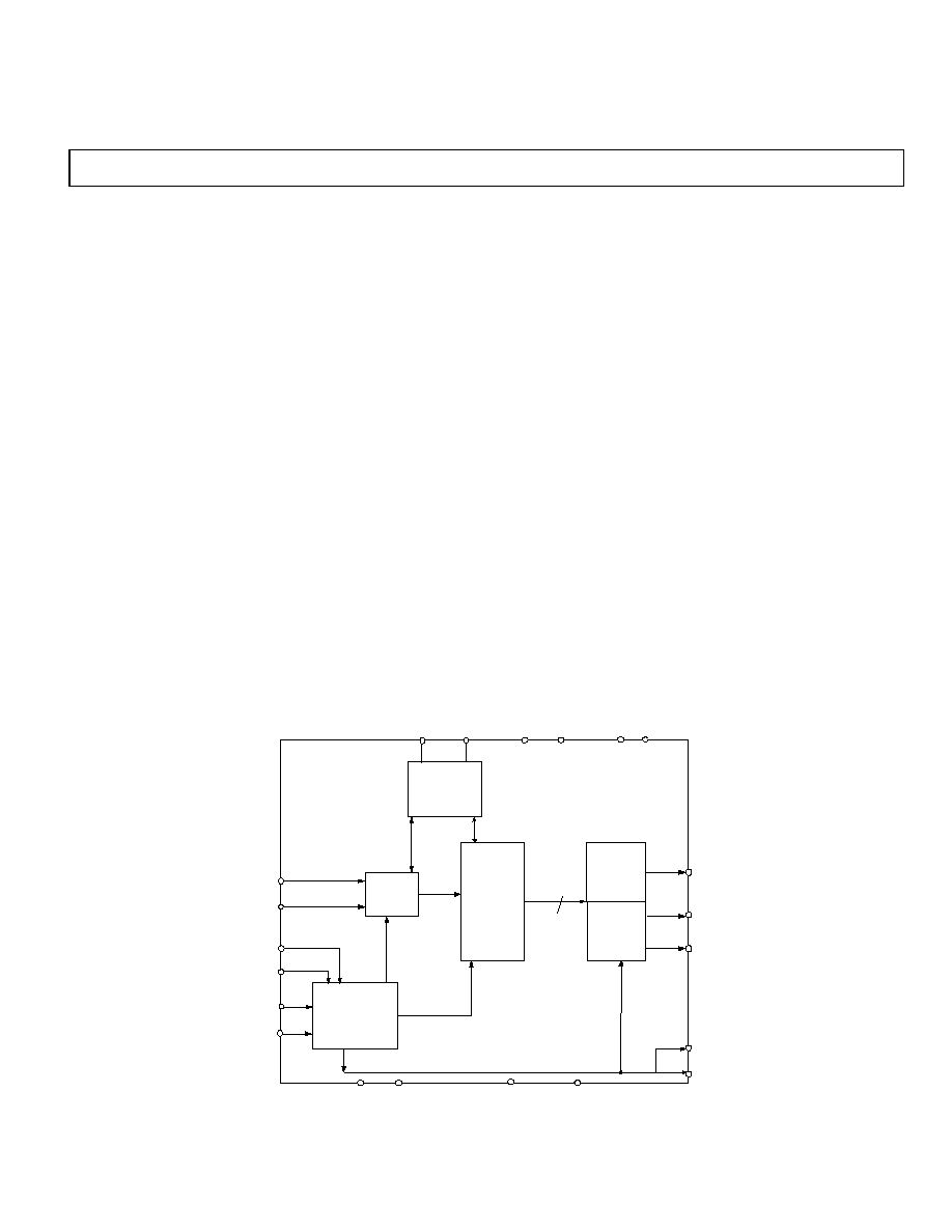
The AD9430 is a 12-bit monolithic sampling analogto
digital converter with an onchip trackandhold circuit and
is optimized for low cost, low power, small size and ease of
use. The product operates up to 170 Msps conversion rate
and is optimized for outstanding dynamic performance in
wideband carrier systems.
The ADC requires a +3.3V power supply and a differential
encode clock for full performance operation. No external
reference or driver components are required for many
applications. The digital outputs are TTL/CMOS or LVDS
compatible. Separate output power supply pins support
interfacing with 3.3V CMOS logic.
An output data format select option of two's complement or
offset binary is supported. In CMOS mode two output buses
support demultiplexed data up to 85 Msps rates. A data sync
input is supported for proper output data port alignment and
a data clock output is available for proper output data timing.
Fabricated on an advanced BiCMOS process, the AD9430 is
available in a 100 pin surface mount plastic package (100
TQFP ePAD) specified over the industrial temperature range
(40°C to +85°C).
LVDS
Outputs
CMOS
Outputs
S2
DrV
DD
AV
DD
DS-
DS+
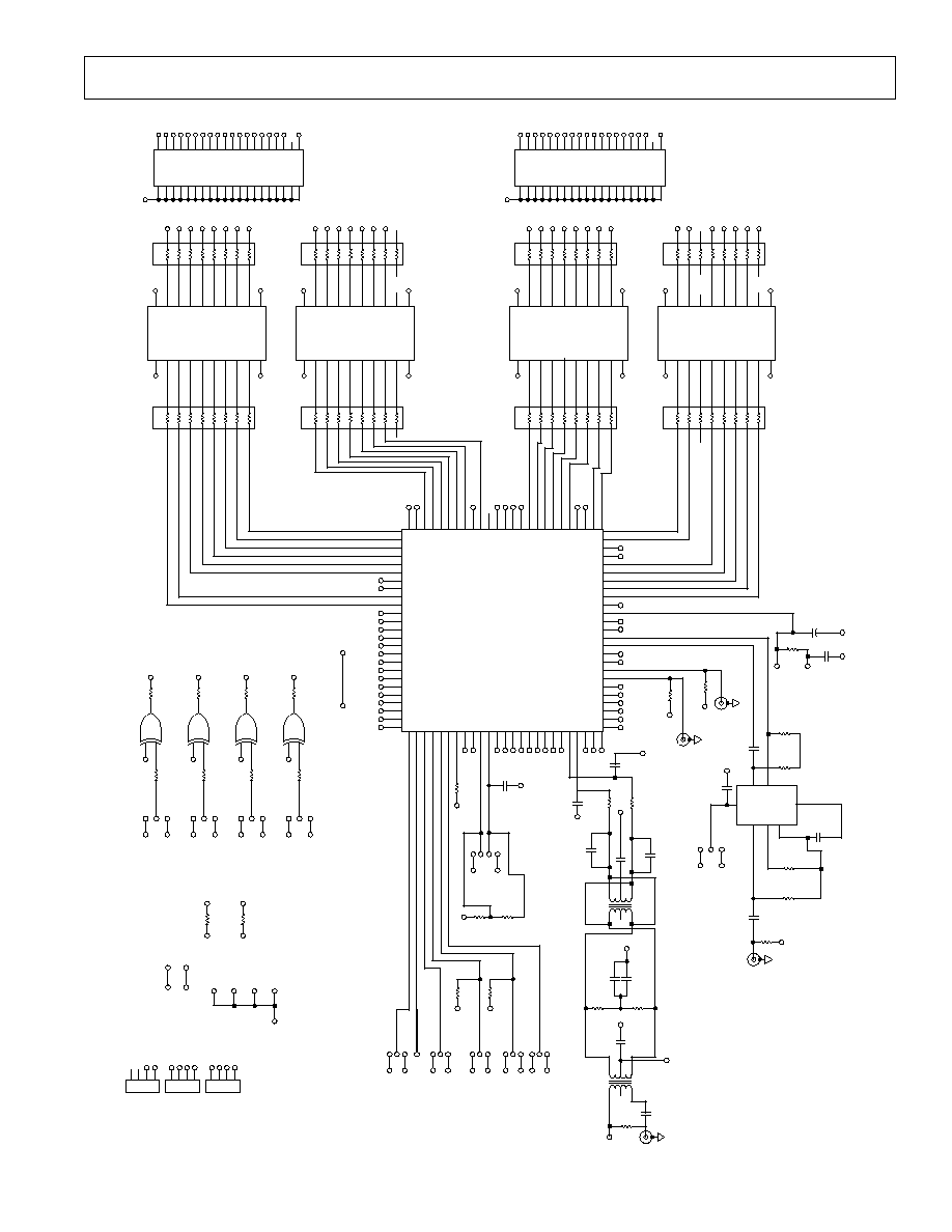
Data(24), OR(2)
12
Scaleable
Reference
ADC
12-bit
Pipeline
Core
Track &
Hold
Clock
Management
AIN+
AIN-
ENC+
ENC-
S4
SENSE
VREF
DrGND
AGND
AD9430
S1
S5
DCO-
DCO+
A port
B port
Data(12), OR(1)
Data(12), OR(1)
Select CMOS or LVDS
AD9430 FUNCTIONAL BLOCK DIAGRAM
REV. PrG 4/01/2002
Information furnished by Analog Devices is believed to be accurate and
reliable.However,no responsibility is assumed by Analog Devices for its use,nor
for any infringements of patents or other rights of third parties that may result from
its use.No license is granted by implication or otherwise under any patent or
patent rights of Analog Devices.
One Technology Way,P.O.Box 9106,Norwood,MA 02062-9106,U.S.A.
Tel:781/329-4700 www.analog.com
Fax:781/326-8703 © Analog Devices, Inc., 2002
PRELIMINARY TECHNICAL DATA
AD9430
-2- 4/01/2002 REV. PrG
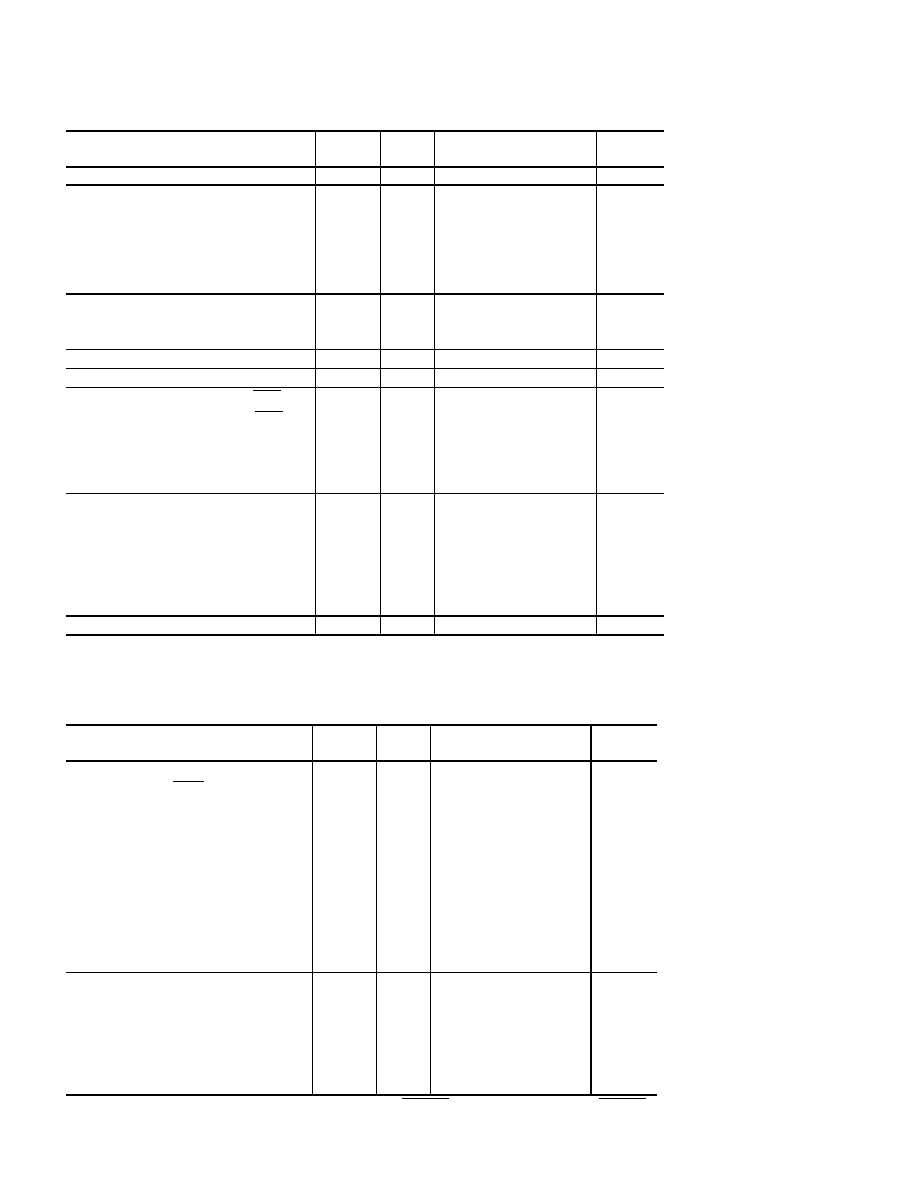
DC SPECIFICATIONS
(AV
DD
= DrV
DD
= 3.3V; T
MIN
= -40
°
C, T
MAX
= +85
°
C, Fin = -0.5dBFS, 1.235V External
reference, LVDS Output Mode
)
Parameter
Temp
Test
Level
AD9430BSV-170
Min Typ Max
Units
RESOLUTION
12
Bits
ACCURACY
No Missing Codes
Offset Error
Gain Error
Differential Nonlinearity (DNL)
Integral Nonlinearity (INL)
Full
25
°
C
25
°
C
25
°
C
25
°
C
I
I
I
I
I
Guaranteed
tbd
tbd
+/- .3
+/- .5
mV
% FS
LSB
LSB
TEMPERATURE DRIFT
Offset Error
Gain Error
Full
Full
V
V
tbd
tbd
ppm/
°
C
ppm/
°
C
POWER SUPPLY REJECTION
Full
V
±
tbd
mV/V
REFERENCE OUT (V
REF
)
Full
V
1.235
V
ANALOG INPUTS (AIN,
AIN
)
Input Voltage Range (AIN
AIN
)
1
Input Common Mode Voltage
Input Resistance
Input Capacitance
Full
Full
Full
Full
V
V
V
V
± .
768
2.8
3
5
V
V
k
pF
POWER SUPPLY
Supply Voltages
AV
DD
DrV
DD
Supply Current
I
ANALOG
(
AV
DD
= 3.3V)
2
I
DIGITAL
(DrVDD = 3.3V)
2
Full
Full
Full
Full
V
V
V
V
3.0 3.3 3.6
3.0 3.3 3.6
335
55
V
V
mA
mA
POWER CONSUMPTION
3
Full V 1.29 W
NOTES
1
Nominal Differential Full Scale = .766 V * 2 = 1.53 V
p-p differential
for S5 = 0; Nominal Differential Full Scale = .766 V
p-p d ifferential
for S5 = 1 (see Fig. X)
2 I
AVDD
and I
DrVDD
are measured with an analog input of 10.3MHz, -0.5dBFs, sine wave, rated Encode rate and in LVDS output mode. See Typical Performance
Characteristics and Applications section for I
DrVDD
. 3 Power Consumption is measured with a DC input at rated Encode rate in LVDS output mode
DIGITAL SPECIFICATIONS
(
AV
DD
= 3.3V, DrV
DD
= 3.3V; T
MIN
= -40
°°
C, T
MAX
= +85
°°
C)
Parameter (Conditions)
Temp
Test
Level
AD9430BSV-170
Min Typ Max
Units
ENCODE AND DATA SYNC
INPUTS (ENC,
ENC
, DS, DS/ )
Differential Input Voltage
1
Encode Common Mode Voltage
Input Resistance
Input Capacitance
LOGIC INPUTS ( S1,S2,S4,S5 )
Logic `1' Voltage
Logic `0' Voltage
Input Resistance
Input Capacitance
Full
Full
Full
Full
Full
Full
Full
Full
IV
IV
IV
IV
IV
IV
IV
IV
0.2
1.5
5.5
4
2.0
.8
30
4
V
V
k
pF
V
V
k
pF
LOGIC OUTPUTS (Demux Mode)
Logic "1" Voltage
2
Logic "0" Voltage
2
LOGIC OUTPUTS (LVDS Mode)
2,3
V
OD
Differential Output Voltage
V
OS
Output Offset Voltage
Output Coding
Full
Full
Full
Full
Full
IV
IV
IV
IV
IV
DrV
DD
-0.05
0.05
247 454
1.125 1.375
Two's Comp or Binary
V
V
mV
V
NOTES
1
All AC specifications tested by driving ENCODE and ENCODE differentially | ENCODE - ENCODE
| > 200mV
2
Digital Output Logic Levels:
DrV
DD
= 3.3V
, C
LOAD
= 5pF.
3
LVDS Rl=100 ohms, LVDS Output Swing Set Resistor = 3.7K
PRELIMINARY TECHNICAL DATA
AD9430
REV. PrG 4/01/2002
-3-
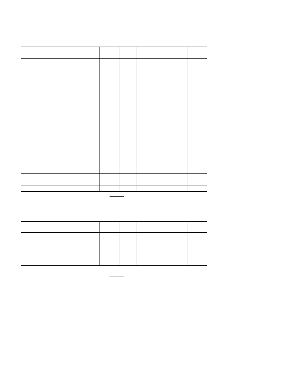
AC SPECIFICATIONS
1
(AV
DD
= 3.3 V, DrV
DD
= 3.3V; ENCODE = Maximum Conversion Rate ; T
MIN
= -40
°
C, T
MAX
= +85
°
C, Internal voltage reference, LVDS Output Mode )
Parameter (Conditions)
Temp
Test
Level
AD9430BSV-170
Min Typ Max
Units
SNR
Analog Input 10 MHz
@ -0.5dBFS 65 MHz
100 MHz
240 MHz
25
°
C
25
°
C
25
°
C
25
°
C
I
I
V
V
65
65
65
64
dB
dB
dB
dB
SINAD
Analog Input 10 MHz
@ -0.5dBFS 65 MHz
100 MHz
240 MHz
25
°
C
25
°
C
25
°
C
25
°
C
I
I
V
V
65
65
64.5
60
dB
dB
dB
dB
Worst Harmonic (2
nd
or 3
rd
)
Analog Input 10 MHz
@ -0.5dBFS 65 MHz
100 MHz
240 MHz
25
°
C
25
°
C
25
°
C
25
°
C
I
I
V
V
-85
-80
-77
-63
dBc
dBc
dBc
dBc
Worst Harmonic (4
th
or higher)
Analog Input 10 MHz
@ -0.5dBFS 65 MHz
100 MHz
240 MHz
25
°
C
25
°
C
25
°
C
25
°
C
I
I
V
V
-87
-87
-77
-63
dBc
dBc
dBc
dBc
Two-tone IMD
2
F1, F2 @ -7 dBFS
Full
V
-75
dBc
Analog Input Bandwidth
25
°
C
V
700
MHz
NOTES
1
All AC specifications tested by driving ENCODE and ENCODE
differentially.
2 F1 = 31.5 MHz, F2 = 32.5 MHz
SWITCHING SPECIFICATIONS
(AV
DD
= 3.3 V, DrV
DD
= 3.3V; ENCODE = Maximum Conversion Rate ;
T
MIN
= -40
°
C, T
MAX
= +85
°
C )
Parameter (Conditions)
Temp
Test
Level
AD9430BSV-170
Min Typ Max
Units
Maximum Conversion Rate
1
Minimum Conversion Rate
1
Encode Pulse Width High (t
EH
)
1
Encode Pulse Width Low (t
EL
)
1
DS Input Setup Time (t
SDS
)
2
DS Input Hold Time (t
HDS
)
2
Full
Full
Full
Full
Full
Full
I
V
V
V
IV
IV
170
40
2
2
.5
1.5
MSPS
MSPS
nS
nS
nS
nS
NOTES
1
All AC specifications tested by driving ENCODE and ENCODE
differentially, LVDS Mode.
2 DS inputs used in CMOS Mode only.
PRELIMINARY TECHNICAL DATA
AD9430
-4- 4/01/2002 REV. PrG
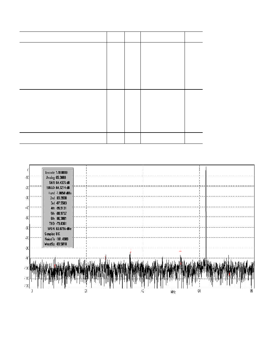
SWITCHING SPECIFICATIONS (cont'd)
Parameter
Temp
Test
Level
AD9430BSV-170
Min Typ Max
Units
OUTPUT Parameters in Demux Mode
Valid Time (t
V
)
Propagation Delay (t
PD
)
Rise Time (t
R
) (20% to 80%)
Fall Time (t
F
) (20% to 80%)
DCO Propagation Delay (t
CPD
)
Data to DCO Skew (t
PD
t
CPD
)
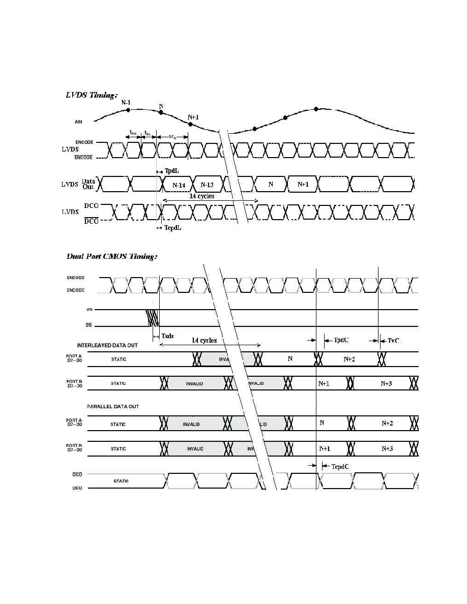
Interleaved Mode (A, B Latency)
Parallel Mode (A, B Latency)
Full
Full
25
°
C
25
°
C
Full
Full
Full
Full
IV
IV
V
V
VI
IV
VI
VI
tbd
3.8
1
1
3.8
0
14/14
14/15
ns
ns
ns
ns
ns
ns
Cycles
Cycles
OUTPUT Parameters in LVDS Mode
Valid Time (t
V
)
Propagation Delay (t
PD
)
Rise Time (t
R
) (20% to 80%)
Fall Time (t
F
) (20% to 80%)
DCO Propagation Delay (t
CPD
)
Data to DCO Skew (t
PD
t
CPD
)
Pipeline Latency
Full
Full
25
°
C
25
°
C
Full
Full
Full
IV
I
V
V
VI
IV
VI
2.0
3.2 4.3
.5
.5
1.8 2.7 3.8
.5
14
ns
ns
ns
ns
ns
ns
Cycles
Aperture Delay (t
A
)
Aperture Uncertainty (Jitter, t
J
)
25
°
C
25
°
C
V
V
1.2
0.25
ps
ps rms
Measured Preliminary Performance : FFT 65MHz Ain at 170MSPS
PRELIMINARY TECHNICAL DATA
AD9430
REV. PrG 4/01/2002 -5-
AD9430 Timing Diagram
PRELIMINARY TECHNICAL DATA
AD9430
-6- 4/01/2002 REV. PrG
ABSOLUTE MAXIMUM RATINGS
AVDD, DRVDD.. .. . . . . . . . . . . . . . . . . . . . . . . . . . . . . . 4 V
Analog Inputs . . . . . . . . . . .. . .. . . 0.5 V to AVDD + 0.5 V
Digital Inputs . . .. . . . . . . . .. . . .. 0.5 V to DRVDD + 0.5 V
REFIN Inputs . . . . . . . . . . . . . . . . 0.5 V to AVDD + 0.5 V
Digital Output Current . . . . . . . . . . . . . . . . . . . . . . . . 20 mA
Operating Temperature . . . . . . . . . . ... . . . . . 55C to +125C
Storage Temperature . . . . . . . . . . . . . ... . . . . 65C to +150C
Maximum Junction Temperature . . . . . . . . . . . . . . . . . 150C
Maximum Case Temperature . . . . . . . . . . . . . . . . . . . ..150C
JA
2
. . . . . . .. . . . . . . . . . . . . . . . . . . . . . . . . 25C/W, 32C/W
NOTES
EXPLANATION OF TEST LEVELS
Test Level
I 100% production tested.
II 100% production tested at 25C and sample tested at
specified temperatures.
III Sample tested only.
IV Parameter is guaranteed by design and characterization
testing.
V Parameter is a typical value only.
VI 100% production tested at 25C; guaranteed by design
and characterization testing for industrial temperature
range; 100% production tested at temperature extremes
for military devices.
1
Stresses above those listed under Absolute Maximum Ratings may
cause
permanent damage to the device. This is a stress rating only; functional
operation of the device at these or any other conditions outside of those
indicated in the operation sections of this specification is not implied.
Exposure to absolute maximum ratings for extended periods may affect
device reliability
.
2
Typical
JA
=
32C/W (heat slug not soldered), Typical
JA
=
25C/W (heat slug soldered), for multilayer board in still air.
CAUTION
ESD (electrostatic discharge) sensitive device. Electrostatic charges as high as 4000 V readily
accumulate on the human body and test equipment and can discharge without detection. Although
the AD9430 features proprietary ESD protection circuitry, permanent damage may occur on
devices subjected to high-energy electrostatic discharges. Therefore, proper ESD precautions are
recommended to avoid performance degradation or loss of functionality
.
ORDERING GUIDE
Model
Temperature Range
Package Option
AD9430BSV-170
40°C to +85°C
TQFP100
AD9430/PCB-CMOS
+25°C
Evaluatio n Board
(CMOS Mode)
Table 1. AD9430 Output Select Coding
S1
(Data
Format
Select)
1
S2
(LVDS/CMOS
Output Mode
Select )
S4
(Select
Interleaved or
Parallel Mode)
2
S5
(Full Scale
Adjust)
Mode
1
X
X
X
2's Complement
0
X
X
X
Offset Binary
X
0
1
X
Dual Mode CMOS Interleaved
X
0
0
X
Dual Mode CMOS Parallel
X
1
X
X
LVDS Mode
X
X
X
1
Full Scale -> .766 V
pp differential
1.533 V
pp
Single- Ended
X
X
X
0
Full Scale -> 1.533 V
pp differential
Notes:
1
X = Don't Care
S1-S5 all have 30K resistive pulldowns on chip
2
In interleaved mode output data on port A is offset from output data changes on port B by ½ output clock cycle.
Interleaved mode
Parallel Mode
PRELIMINARY TECHNICAL DATA
AD9430
REV. PrG 4/01/2002 -7-
AD9430
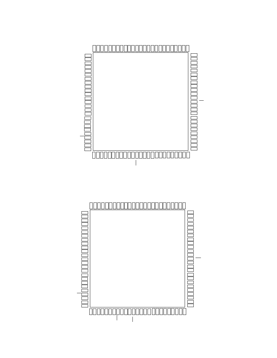
LVDS PINOUT
TOP VIEW
(Not to Scale)
11
S5
S4
AGND
S2
S1
LVDSBIAS
AVDD
AGND
13
4
5
6
7
12
8
9
2
3
14
10
15
1
SENSE
VREF
AGND
AGND
AVDD
16
AVDD
DNC
AGND 17
18
19
20
21
22
23
24
25
AGND
AVDD
AGND
AIN
AIN
AVDD
AGND
AVDD
AGND
DRVDD
D8_T
D8_C
D7_T
D7_C
D6_T
D6_C
DRGND
D5_T
D5_C
DCO
DCO
DRVDD
DRGND
65
63
72
71
70
69
64
68
67
74
73
62
66
61
75
DRGND
60 D4_T
59
D4_C
58 D3_T
57 D3_C
56 D2_T
55 D2_C
54 DRVDD
53 DRGND
52 D1_T
51 D1_C
36
AGND
AVDD
AVDD
AGND
AGND
GND
AVDD
AVDD
AGND
38
29
30
31
32
37
33
34
27
28
39
35
40
26
ENC
AGND
AVDD
AVDD
41
AGND
AVDD
42
43
44
45
46
47
48
49
50
DNC
DNC
DNC
DNC
DNC
DRVDD
DRGND
D0_C
D0_T
ENC
AGND
AVDD
AVDD
AGND
AGND
OR_T
OR_C
DRGND
D11_T
D11_C
D10_T
D10_C
D9_T
81
79
88
87
86
85
80
84
83
90
89
78
82
77
91
AVDD
76
D9_C
97
96
95
94
93
92
99
98
100
AGND
AVDD
AGND
AGND
AVDD
AVDD
AGND
AGND
AVDD
DRVDD
(MSB)
AD9430 LVDS Mode Pinout
AD9430
CMOS PINOUT
TOP VIEW
(Not to Scale)
11
S5
S4
AGND
S2
S1
DNC
AVDD
AGND
13
4
5
6
7
12
8
9
2
3
14
10
15
1
SENSE
VREF
AGND
AGND
AVDD
16
AVDD
DNC
AGND 17
18
19
20
21
22
23
24
25
AGND
AVDD
AGND
AIN
AIN
AVDD
AGND
AVDD
AGND
DRVDD
DA4
DA3
DA2
DA1
DA0
DNC
DRGND
DNC
DNC
DCO
DCO
DRVDD
DRGND
65
63
72
71
70
69
64
68
67
74
73
62
66
61
75
DRGND
60 OR_B
59
DB11
58 DB10
57 DB9
56 DB8
55 DB7
54 DRVDD
53
(MSB)
52 DB6
51 DB5
DRGND
36
AGND
AVDD
AVDD
AGND
AGND
DS
DS
AVDD
AGND
38
29
30
31
32
37
33
34
27
28
39
35
40
26
ENC
AGND
AVDD
AVDD
41
AGND
AVDD
42
43
44
45
46
47
48
49
50
DNC
DNC
DB0
DB1
DB2
DRVDD
DRGND
DB3
DB4
ENC
AGND
AVDD
AVDD
AGND
AGND
DA11
(MSB)
DRVDD
DRGND
DA10
DA9
DA8
DA7
DA6
81
79
88
87
86
85
80
84
83
90
89
78
82
77
91
AVDD
76
DA5
97
96
95
94
93
92
99
98
100
AGND
AVDD
AGND
AGND
AVDD
AVDD
AGND
AGND
AVDD
OR_A
AD9430 CMOS Dual Mode Pinout
PRELIMINARY TECHNICAL DATA
AD9430
-8- 4/01/2002 REV. PrG
PIN FUNCTION DESCRIPTIONS (CMOS mode)
CMOS Mode
Pin Number
Name
Function in CMOS Mode
2,7,42,43,65,66,68
DNC
Do not connect
1
S5
Full Scale Adjust pin : `1' sets FS =
.766 V
pp differential,
`0' sets FS =
1.533 V
pp differential
3
S4
Interlaced or parallel output mode. (only in Dual Port mode
operation) HIGH = data arrives in channel A at falling edge of clock
and data arrives in channel A at rising edge of clock. LOW = data
arrives in channels A and B at rising edge of clock.
5
S2
Output Mode select. Low = Dual Port, CMOS; High = LVDS
6
S1
Data format select. Low = Binary, High = Two's compliment
8,14,15,18,19,24,27,28,29,34,
39,40,88,89,90,94,95,98,99
AV
DD
3.3V analog supply. (3.0V to 3.6V)
4,9,12,13,16,17,20,23,25,26,3
0,31,35,38,41,86,87,91,92,93,
96,97,100
AGND
Analog Ground
10
SENSE
Control Pin for Reference , Full Scale
11
VREF
1.235 Reference I/O - function dependent on REFSENSE
21
VIN+
Analog input true.
22
VIN-
Analog input compliment.
32
DS+
Data sync (input) true. Aligns output channels so that data from
channel A represents a sample that is prior from data in channel B,
taking into account the pipeline delay. (See timing diagram). Tie
LOW if not used.
33
DS-
Data sync (input) compliment. Tie HIGH if not used.
36
ENC+
Clock input true.
37
ENC-
Clock input compliment.
44
DB0
B Port Output Data Bit (LSB)
45
DB1
B Port Output Data Bit
46
DB2
B Port Output Data Bit
49
DB3
B Port Output Data Bit
50
DB4
B Port Output Data Bit
51
DB5
B Port Output Data Bit
52
DB6
B Port Output Data Bit
55
DB7
B Port Output Data Bit
56
DB8
B Port Output Data Bit
57
DB9
B Port Output Data Bit
58
DB10
B Port Output Data Bit
59
DB11
B Port Output Data Bit (MSB)
60
OR_B
B Port Overrange
48,53,61,67,74,82
DrGND
Digital ground.
47,54,62,75,83
DrV
DD
3.3V digital output supply. (3.0V to 3.6V)
63
DCO-
Data Clock output compliment.
64
DCO+
Data Clock output true.
69
DA0
A port Output Data Bit (LSB)
70
DA1
A port Output Data Bit
71
DA2
A port Output Data Bit
72
DA3
A port Output Data Bit
73
DA4
A port Output Data Bit
76
DA5
A port Output Data Bit
77
DA6
A port Output Data Bit
78
DA7
A port Output Data Bit
79
DA8
A port Output Data Bit
80
DA9
A port Output Data Bit
81
DA10
A port Output Data Bit
84
DA11
A port Output Data Bit (MSB)
85
OR_A
A port Overrange

PRELIMINARY TECHNICAL DATA
AD9430
REV. PrG 4/01/2002 -9-
PIN FUNCTION DESCRIPTIONS (LVDS mode )
LVDS Mode
Pin Number
Name
Function in LVDS Mode
2,42,43,44,45,46
DNC
Do not connect
1
S5
Full Scale Adjust pin : `1' sets FS =
.766 V
pp differential,
`0' sets FS =
1.533 V
pp differential
3
S4
Interlaced or parallel output mode. (only in Dual Port mode
operation) HIGH = data arrives in channel A at falling edge of clock
and data arrives in channel A at rising edge of clock. LOW = data
arrives in channels A and B at rising edge of clock.
5
S2
Output Mode select. Low = Dual Port, CMOS; High = LVDS
6
S1
Data format select. Low = Binary, High = Two's compliment
7
LVDSBIAS
Sets LVDS Output Current = 3.5mA
(Place 3.7K RSET resistor from LVDSBIAS to ground)
8,14,15,18,19,24,27,28,29,34,
39,40,88,89,90,94,95,98,99
AV
DD
3.3V analog supply. (3.0V to 3.6V)
4,9,12,13,16,17,20,23,25,26,3
0,31,35,38,41,86,87,91,92,93,
96,97,100
AGND
Analog Ground
10
SENSE
Control Pin for Reference , Full Scale
11
VREF
1.235 Reference I/O - function dependent on REFSENSE
21
VIN+
Analog input true.
22
VIN-
Analog input compliment.
32
DS+
Data sync (input) Not used in LVDS mode.Tie LOW .
33
DS-
Data sync (input) compliment. Not used in LVDS mode.Tie HIGH.
36
ENC+
Clock input true. (LVPECL levels)
37
ENC-
Clock input compliment. (LVPECL levels)
47,54,62,75,83
DrV
DD
3.3V digital output supply.
48,53,61,67,74,82
DrGND
Digital ground.
49
D0_C
D0 complement output bit (LSB) (LVDS Levels)
50
D0_T
D0 true output bit (LSB) (LVDS Levels)
51
D1_C
D1 complement output bit (LVDS Levels)
52
D1_T
D1 true output bit (LVDS Levels)
55
D2_C
D2 complement output bit (LVDS Levels)
56
D2_T
D2 true output bit (LVDS Levels)
57
D3_C
D3 complement output bit (LVDS Levels)
58
D3_T
D3 true output bit (LVDS Levels)
59
D4_C
D4 complement output bit (LVDS Levels)
60
D4_T
D4 true output bit (LVDS Levels)
63
DCO-
Data Clock output compliment. (LVDS Levels)
64
DCO+
Data Clock output true. (LVDS Levels)
65
D5_C
D5 complement output bit (LVDS Levels)
66
D5_T
D5 true output bit (LVDS Levels)
68
D6_C
D6 complement output bit (LVDS Levels)
69
D6_T
D6 true output bit (LVDS Levels)
70
D7_C
D7 complement output bit (LVDS Levels)
71
D7_T
D7 true output bit (LVDS Levels)
72
D8_C
D8 complement output bit (LVDS Levels)
73
D8_T
D8 true output bit (LVDS Levels)
76
D9_C
D9 complement output bit (LVDS Levels)
77
D9_T
D9 true output bit (LVDS Levels)
78
D10_C
D10 complement output bit (LVDS Levels)
79
D10_T
D10 true output bit (LVDS Levels)
80
D11_C
D11 complement output bit (LVDS Levels) MSB
81
D11_T
D11 true output bit (LVDS Levels) MSB
84
OR_C
Overrange complement output bit (LVDS Levels)
85
OR_T
Overrange true output bit (LVDS Levels)

PRELIMINARY TECHNICAL DATA
AD9430
-10- 4/01/2002 REV. PrG
TERMINOLOGY
Analog Bandwidth
The analog input frequency at which the spectral power of
the fundamental frequency (as determined by the FFT
analysis) is reduced by 3 dB.
Aperture Delay
The delay between the 50% point of the rising edge of the
ENCODE command and the instant at which the analog
input is sampled.
Aperture Uncertainty (Jitter)
The sample-to-sample variation in aperture delay.
Crosstalk
Coupling onto one channel being driven by a low level (40
dBFS) signal when the adjacent interfering channel is driven
by a full-scale signal.
Differential Analog Input Resistance, Differential Analog
Input Capacitance and Differential Analog Input
Impedance
The real and complex impedances measured at each analog
input port. The resistance is measured statically and the
capacitance and differential input impedances are measured
with a network analyzer.
Differential Analog Input Voltage Range
The peak-to-peak differential voltage that must be applied to
the converter to generate a full-scale response. Peak
differential voltage is computed by observing the voltage on
a single pin and subtracting the voltage from the other pin,
which is 180 degrees out of phase. Peak-to-peak differential
is computed by rotating the inputs phase 180 degrees and
again taking the peak measurement. The difference is then
computed between both peak measurements.
Differential Nonlinearity
The deviation of any code width from an ideal 1 LSB step.
Effective Number of Bits
The effective number of bits (ENOB) is calculated from the
measured SNR based on the equation:
02
.
6
76
.
1
dB
SNR
ENOB
MEASURED
-
=
ENCODE Pulsewidth / Duty Cycle
Pulsewidth high is the minimum amount of time that the
ENCODE pulse should be left in Logic 1 state to achieve
rated performance; pulsewidth low is the minimum time
ENCODE pulse should be left in low state. See timing
implications of changing t
ENCH
in text. At a given clock rate,
these specifica-tions define an acceptable ENCODE duty
cycle.
Full-Scale Input Power
Expressed in dBm. Computed using the following equation:
=
001
.
log
10
2
Input
Fullscale
Fullscale
Z
V
Power
rms
Gain Error
Gain error is the difference between the measured and ideal
full scale input voltage range of the ADC.
Harmonic Distortion, Second
The ratio of the rms signal amplitude to the rms value of the
second harmonic component, reported in dBc.
Harmonic Distortion, Third
The ratio of the rms signal amplitude to the rms value of the
third harmonic component, reported in dBc.
Integral Nonlinearity
The deviation of the transfer function from a reference line
measured in fractions of 1 LSB using a "best straight line"
determined by a least square curve fit.
Minimum Conversion Rate
The encode rate at which the SNR of the lowest analog
signal frequency drops by no more than 3 dB below the
guaranteed limit.
Maximum Conversion Rate
The encode rate at which parametric testing is performed.
Output Propagation Delay
The delay between a differential crossing of ENCODE and
ENCODE and the time when all output data bits are within
valid logic levels.
Noise (for Any Range within the ADC)
-
-
=
10
10
*
001
.
*
dBFS
dBc
dBm
Signal
SNR
FS
noise
Z
V
Where Z is the input impedance, FS is the full scale of the
device for the frequency in question, SNR is the value for the
particular input level, and Signal is the signal level within
the ADC reported in dB below full scale. This value includes
both thermal and quantization noise.
Power Supply Rejection Ratio
The ratio of a change in input offset voltage to a change in
power supply voltage.
Signal -to-Noise-and-Distortion (SINAD)
The ratio of the rms signal amplitude (set 1 dB below full
scale) to the rms value of the sum of all other spectral
components, including harmonics but excluding dc.
PRELIMINARY TECHNICAL DATA
AD9430
REV. PrG 4/01/2002 -11-
Signal -to-Noise Ratio (without Harmonics)
The ratio of the rms signal amplitude (set at 1 dB below full
scale) to the rms value of the sum of all other spectral
components, excluding the first five harmonics and dc.
Spurious-Free Dynamic Range (SFDR)
The ratio of the rms signal amplitude to the rms value of the
peak spurious spectral component. The peak spurious
component may or may not be a harmonic. May be reported
in dBc (i.e., degrades as signal level is lowered), or dBFS
(always related back to converter full scale).
Two-Tone Intermodulation Distortion Rejection
The ratio of the rms value of either input tone to the rms
value of the worst third order intermodulation product;
reported in dBc.
Two-Tone SFDR
The ratio of the rms value of either input tone to the rms
value of the peak spurious component. The peak spurious
component may or may not be an IMD product. May be
reported in dBc (i.e., degrades as signal level is lowered), or
in dBFS (always related back to converter full scale).
Worst Other Spur
The ratio of the rms signal amplitude to the rms value of the
worst spurious component (excluding the second and third
harmonic) reported in dBc.
Transient Response Time
Transient response is defined as the time it takes for the
ADC to reacquire the analog input after a transient from
10% above negative full scale to 10% below positive full
scale.
Out-of-Range Recovery Time
Out of range recovery time is the time it takes for the ADC
to reacquire the analog input after a transient from 10%
above positive full scale to 10% above negative full scale, or
from 10% below negative full scale to 10% below positive
full scale.
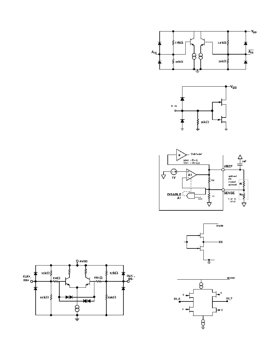
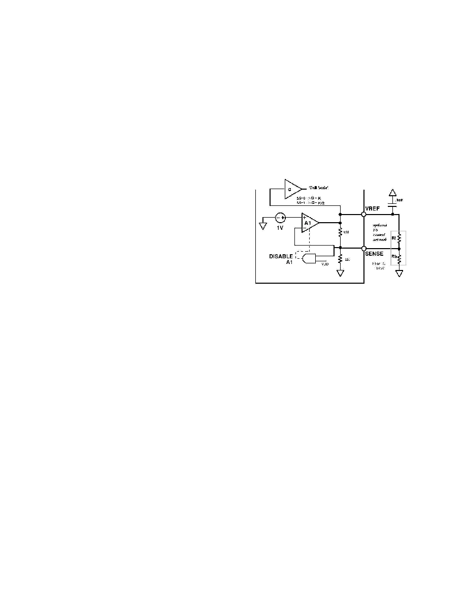
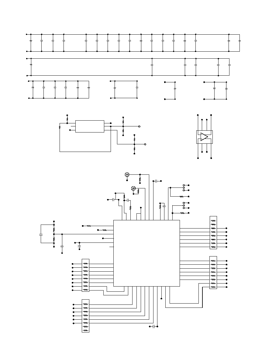
EQUIVALENT CIRCUITS
Figure X Encode and DS Inputs
Figure X Analog Inputs
Figure X S1-S5 Inputs
Figure X VREF, SENSE I/O
Figure X Data Outputs (CMOS Mode)
Figure X Data Outputs (LVDS Mode)
PRELIMINARY TECHNICAL DATA
AD9430
-12- 4/01/2002 REV. PrG
APPLICATION NOTES
THEORY OF OPERATION
The AD9430 architecture is optimized for high speed and
ease of use. The analog inputs drive an integrated high
bandwidth track-and-hold circuit that samples the signal
prior to quantization by the 12-bit core. For ease of use the
part includes an onboard reference and input logic that
accepts TTL, CMOS, or LVPECL levels. The digital outputs
logic levels are user selectable as standard 3V CMOS or
LVDS (ANSI-644 compatible) via pin S2.
USING THE AD9430
ENCODE Input
Any high speed A/D converter is extremely sensitive to the
quality of the sampling clock provided by the user. A
track/hold circuit is essentially a mixer, and any noise,
distortion, or timing jitter on the clock will be combined
with the desired signal at the A/D output. For that reason,
considerable care has been taken in the design of the
ENCODE input of the AD9430, and the user is advised to
give commensurate thought to the clock source.
The AD9430 has an internal clock duty cycle stabilization
circuit that locks to the rising edge of ENCODE (falling
edge of ENCODE if driven differentially), and optimizes
timing internally. This allows for a wide range of input duty
cycles at the input without degrading performance. Jitter in
the rising edge of the input is still of paramount concern, and
is not reduced by the internal stabilization circuit. This
circuit is always on, and cannot be disabled by the user.
The ENCODE and ENCODE inputs are internally biased to
1.5V (nominal), and support either differential or single
ended signals. For best dynamic performance, a differential
signal is recommended. Good performance is obtained
using an MC10EL16 in the circuit to drive the
encode inputs , as illustrated in figure below.
Driving Encode with EL16
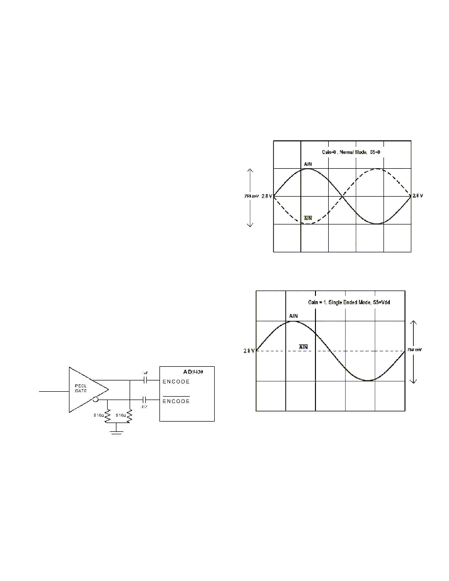
Analog Input
The analog input to the AD9430 is a differential buffer. For
best dynamic performance, impedances at
AIN
and
____
AIN
should match. The analog input has been optimized to
provide superior wideband performance and requires that the
analog inputs be driven differentially. SNR and SINAD
performance will degrade significantly (~6dB) if the analog
input is driven with a single-ended signal. A wideband
transformer such as Minicircuits ADT1-1WT can be used to
provide the
differential analog inputs for applications that require a
single-ended-to-differential conversion. Both analog inputs
are self-biased by an on-chip resistor divider to a nominal
2.8 V. (See Equivalent Circuits section TBD.)
Special care was taken in the design of the Analog Input
section of the AD9430 to prevent damage and corruption of
data when the input is overdriven. The nominal input range
is 1.5 V diff p-p. The nominal differential input range is 768
mV p-p × 2.
Differential Analog Input Range
Single Ended Analog Input Range
PRELIMINARY TECHNICAL DATA
AD9430
REV. PrG 4/01/2002 -13-
Digital Outputs
The off chip drivers on the chip can be configured by the
user to provide CMOS or LVDS compatible output levels
via pin S2.
The CMOS digital outputs (S2=0) are TTL/CMOS-
compatible for lower power consumption. The outputs are
biased from a separate supply (VDD), allowing easy
interface to external logic. The outputs are CMOS devices
which will swing from ground to VDD (with no dc load). It
is recommended to minimize the capacitive load the ADC
drives by keeping the output traces short (<1 inch, for a total
C
LOAD
< 5 pF). When operating in cmos mode it is also
recommended to place low value (220 ohm) series damping
resistors on the data lines to reduce switching transient
effects on performance.
LVDS outputs are available when S2=VDD and a 3.7K
RSET resistor is placed at pin 7 ( LVDSBIAS) to ground .
This resistor sets the output current at each output equal to a
nominal 3.5mA ( 10* I
RSET
) . A 100 ohm differential
termination resistor placed at the lvds receiver inputs results
in a nominal 350mV voltage swing at the receiver. Note that
when operating in LVDS mode the output supply must be at
a dc potential greater than or equal to the analog supply level
(AVDD). This can be accomplished simply by biasing the
two supplies from the same power plane or by tying the two
supplies on the pcb through an inductor. When operating in
CMOS mode this is not required and separate supplies are
recommended.
Clock Outputs (DCO+, DCO-)
The input ENCODE is divided by two (in CMOS mode) and
available off-chip at DCO+ and DCO-. These clocks can
facilitate latching off-chip, providing a low skew clocking
solution (see timing diagram). The on-chip clock buffers
should not drive more than 5 pF of capacitance to limit
switching transient effects on performance.
Note that the Outputs clocks are CMOS levels when CMOS
mode is selected(S2=0) and are LVDS levels when in LVDS
mode(S2=VDD). (Requiring a 100ohm differential
termination at receiver in LVDS mode). The output clock in
LVDS mode switches at the encode rate.
Voltage Reference
A stable and accurate 1.25 V voltage reference is built into
the AD9430 (VREF). The analog input Full Scale Range is
linearly proportional to the voltage at VREF. VREF (and in
turn input full scale ) can be varied by adding an external
resistor network at VREF, SENSE and GROUND. (See
figure X ) . No appreciable degradation in performance
occurs when VREF is adjusted ±5%. Note that an external
reference can be used by connecting the SENSE pin to VDD
(disabling internal reference) and driving VREF with the
external reference source. A .1uF capacitor to ground is
recommended at VREF pin in internal and external reference
applications.
Simplified Voltage Reference Equivalent Circuit
PRELIMINARY TECHNICAL DATA
AD9430
-14- 4/01/2002 REV. PrG
AD9430 EVALUATION BOARD
The AD9430 evaluation board offers an easy way to test the
AD9430. It requires a clock source, an analog input signal, and
a 3.3 V power supply. The clock source is buffered on the board
to provide the clocks for the ADC, an on-board DAC, latches,
and a data ready signal. The digital outputs and output clocks
are available at two 40-pin connectors, P3 and P4. The board
has several different modes of operation, and is shipped in the
following configuration:
· Offset Binary
· Internal Voltage Reference
· CMOS Parallel Timing
· Full-Scale Adjust = Low
Power Connector
Power is supplied to the board via a detachable 12-lead power
strip (three 4-pin blocks).
Table II. Power Connector
AVDD 3.3 V
Analog Supply for ADC (~ 350 mA)
DRVDD 3.3 V
Output Supply for ADC (~ 28 mA)
VDL 3.3 V
Supply for Support Logic and DAC (~350 mA)
EXT_VREF
*
Optional External Reference Input
VCLK/V_XTAL
Supply for Clock Buffer/Optional XTAL
VAMP
Supply for Optional Amp
*LVEL16 clock buffer can be powered from AVDD or VCLK at E47 jumper
(AVDD, DrVDD,VDL are the minimum required power connections).
Analog Inputs
The evaluation board accepts a 1.3 V p-p analog input signal
centered at ground at SMB connector J4. This signal is terminated
to ground through 50
by R16. The input can be alternatively
terminated at T1 transformer secondary by R13, R14. T1 is a
wideband RF transformer providing the single-ended to differential
conversion allowing the ADC to be driven differentially, minimizing
even order harmonics. An optional second transformer T2 can be
placed following T1 if desired. This would provide some perfor-
mance advantage (~12 dB) for high analog input frequencies
(>100 MHz). If T2 is placed, two shorting traces at the pads would
need to be cut. The analog signal is low pass filtered by R41,
C12, and R42, C13 at the ADC input.
Gain
Full scale is set at E17E19, E17E18 sets S5 low, full scale =
1.5 V differential; E17E19 sets S5 high, full scale = 0.75 V
differential.
Encode
The encode clock is terminated to ground through 50
at SMB
connector J5. The input is ac-coupled to a high-speed differential
receiver (LVEL16) which provides the required low-jitter, fast
edge rates needed for optimum performance. J5 input should be
> 0.5 V p-p. Power to the EL16 is set at jumper E47. E47E45
powers the buffer from AVDD, E47E46 powers the buffer from
VCLK/V_XTAL.
Voltage Reference
The AD9430 has an internal 1.23 V voltage reference. The
ADC uses the internal reference as the default when jumpers
E24E27 and E25E26 are left open. The full scale can be
increased by placing optional resistor R3. The required value
would vary with process and needs to be tuned for the specific
application. Full scale can similarly be reduced by placing R4;
tuning would be required here as well. An external reference can
be used by shorting the SENSE pin to 3.3 V (place jumper
E26E25). E27E24 jumper connects the ADC VREF pin to
EXT_VREF pin at the power connector.
Data Format Select
Data Format Select sets the output data format of the ADC. Set-
ting DFS (E1E2) low sets the output format to be offset binary;
setting DFS high (E1E3) sets the output to two's complement.
I/P
Output timing is set at E11E13. E12E11 sets S4 low for
parallel output timing mode. E11E13 sets S4 high for interleaved
timing mode.
Timing Controls
Flexibility in latch clocking and output timing is accomplished
by allowing for clock inversion at the timing controls section of
the PCB. Each buffered clock is buffered by an XOR and can be
inverted by moving the appropriate jumper for that clock.
Data Outputs
The ADC digital outputs are latched on the board by four LVT574s;
the latch outputs are available at the two 40-pin connectors at pins
1133 on P23 (channel A) and pins 1133 on P3 (channel B).
The latch output clocks (data ready) are available at Pin 37 on
P23 (channel A) and Pin 37 on P3 (channel B). The data ready
clocks can be inverted at the timing controls section if needed.
CH1
CH2
CH2
M 5.00nS
1
2
: 4.6nS
C1 FREQ
84.65608MHz
2.00V
2.00V
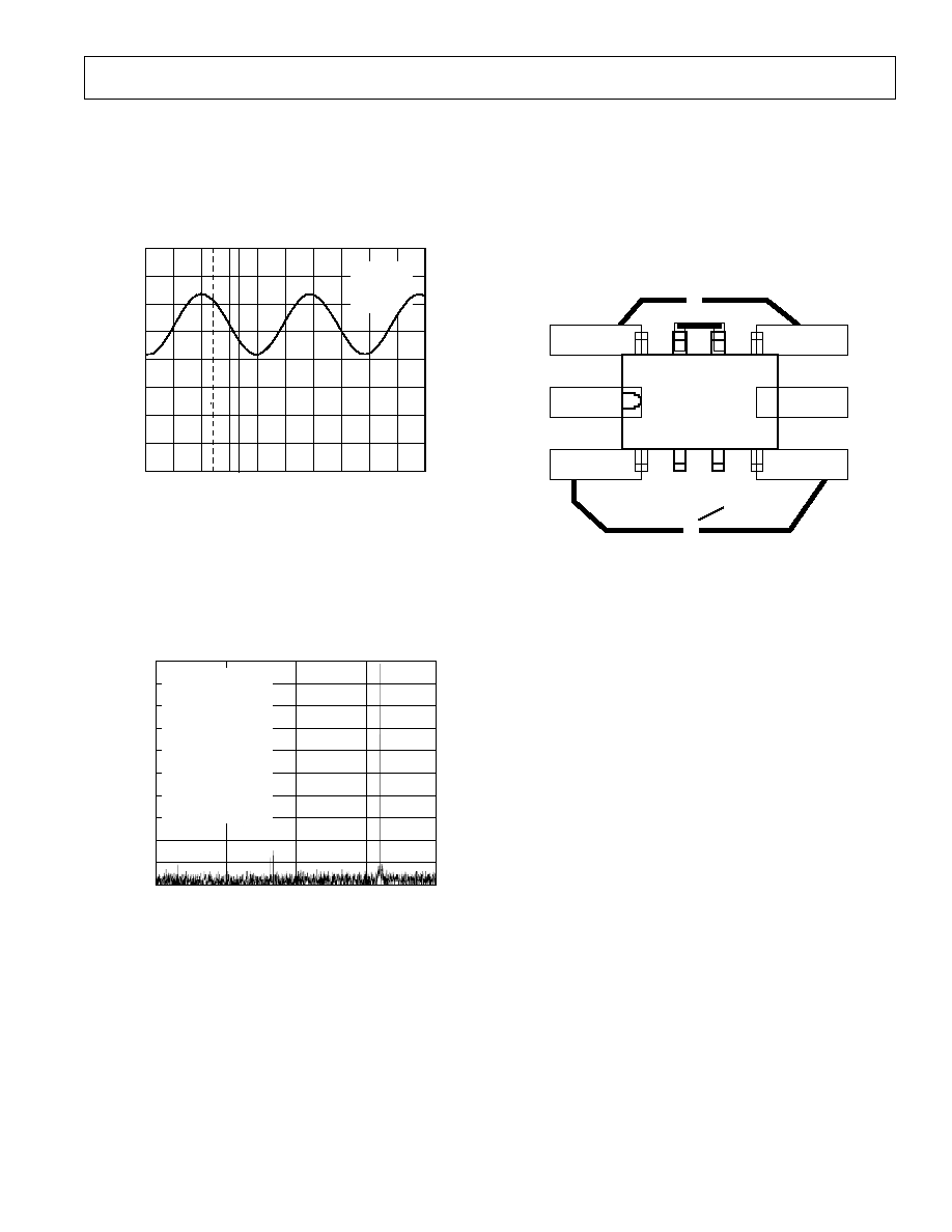
Figure 13. Data Output and Clock @ 80-Pin Connector
PRELIMINARY TECHNICAL DATA
REV. PrG 4/01/2002 -15-
AD9430
DAC Outputs
Each channel is reconstructed by an on-board dual-channel DAC,
an AD9753. This DAC is intended to assist in debug--it should
not be used to measure the performance of the ADC. It is a current
output DAC with on-board 50
termination resistors. The
figure below is representative of the DAC output with a full-scale
analog input. The scope setting is low bandwidth.
CH1
CH1
M 25.0nS
1
C1 FREQ
10.33592MHz
C1 PK-PK
448mV
2.00mV
248mV
Figure 14. DAC Output
Encode Xtal
An optional xtal oscillator can be placed on the board to serve
as a clock source for the PCB. Power to the xtal is through the
VCLK/VXTAL pin at the power connector. If an oscillator is used,
ensure proper termination for best results. The board has been
tested with a Valpey Fisher VF561 and a Vectron JN00158-163.84.
Test results for the VF561 are shown below.
MHz
0
30
0
80
20
dB
40
60
60
80
20
10
50
40
100
90
70
ENCODE 163.84MHz
ANALOG 65.02MHz
SNR 63.93dB
SINAD 63.87dB
FUND 0.45dBFS
2ND 85.62dBc
3RD 91.31dBc
4TH 90.54dBc
5TH 90.56dBc
6TH 91.12dBc
THD 82.21dBc
SFDR 83.93dBc
SAMPLES 8k
NOISEFLR 100.44dBFS
WORSTSP 83.93dBc
Figure 15. FFT--Using VF561 XTAL as Clock Source
Optional Amplifier
The footprint for transformer T2 can be modified to accept a
wideband differential amplifier (AD8350) for low frequency
applications where gain is required. Note that Pin 2 would need
to be lifted and left floating for operation. Input transformer T1
would need to be modified to a 4:1 for impedance matching and
ADC input filtering would enhance performance (see AD8350
data sheet). SNR/SINAD Performance of 61 dB/60 dB is pos-
sible and would start to degrade at about 30 MHz.
CUT TRACE
AD9430
1
CUT TRACE
Figure 16. Using the AD8350 on the AD9430 PCB
PRELIMINARY TECHNICAL DATA
AD9430
-16- 4/01/2002 REV. PrG
Table III. Evaluation Board Bill of Materials
No.
Qty.
Reference Designator
Device
Package
Value
Comments
1
45
C1, C3C11, C15C17,
Capacitor
0603
0.1
µF
C43, C47
C19C29, C31C48,
Not Placed
C58C62
2
0
C2
Capacitor
0603
10 pF
Not Placed
3
0
C12, C13
Capacitor
0603
20 pF
Not Placed
4
1
C14
Capacitor
0603
0.01
µF
5
0
C18
Capacitor
0603
1
µF
6
7
C30, C49, C63C67
Capacitor
CAPL
10
µF
C30 Not Placed
7
9
E3E1E2
3-Pin Header/Jumper
E19E17E18
3-Pin Header/Jumper
E13E11E12
3-Pin Header/Jumper
E26E25E27E24
4-Pin Header
E46E47E45
3-Pin Header/Jumper
E35E33E34
3-Pin Header/Jumper
E32E30E31
3-Pin Header/Jumper
E29E23E28
3-Pin Header/Jumper
E22E16E21
3-Pin Header/Jumper
8
5
J1, J2, J3, J4, J5, J6
SMB
SMB
J1 Not Placed
9
2
P3, P23
40-Pin Header
10
3
P4, P21, P22
4-Pin Power Connector
Post
25.531.3425.0
Wieland
Detachable
Connector
25.602.5453.0
Wieland
11
8
R1, R5, R13, R14, R16,
Resistor
0603
50
R1, R13, R14
Not Placed
R25, R27, R28, R41, R42
12
1
R2, R3, R4
Resistor
0603
3.9 k
R3, R4 Not Placed
13
8
R6R8, R10, R15,
Resistor
0603
100
R15, R21R24, R38
Not Placed
R21R24, R33R36, R38
14
5
R12, R30, R37
Resistor
0603
0
15
4
R17, R18, R19, R20
Resistor
0603
510
16
1
R26
Resistor
0603
2 k
17
1
R29
Resistor
0603
390
18
7
R31, R32, R39, R40, R43,
Resistor
0603
1 k
R44, R45
19
4
RZ1, RZ2, RZ3, RZ4
Resistor Pack 220
SO16RES
742C163221JTR
CTS
20
8
RZ5, RZ6, RZ7, RZ8, RZ9,
Resistor Pack 22
SO16RES
742C163220JTR
CTS
RZ10, RZ11, RZ12
21
1
T1, T2
Transformer
CD542
Minicircuits
T2 Not Placed
ADT11WT
22
1
U1
AD9430BSV
TQFP100
ADC
23
1
U2
MC100LVEL16D
SO8NB
Clock Buffer
24
1
U3
74LCX86
SO14NB
Xor/Buffer
25
4
U4, U5, U6, U7
74LVT574
SO20
Latch
26
1
U9
AD9753AST
LQFP48
DAC
PRELIMINARY TECHNICAL DATA
REV. PrG 4/01/2002 -17-
AD9430
VCC
VEE
DQ
DN
QN
VBB
GND
E45
E46
VCC
VCLK
E47
C36
0.1
F
J5
GND
R27
50
C5
0.15
F
ENCODE
2
3
4
5
6
7
8
C8
0.1
F
R10
510
R17
510
MC100L
VEL 16
U2
GND
R20
510
R19
510
GND
OUT_EN
D0
D1
D2
D3
D4
D5
D6
D7
GND
VCC
Q0
Q1
Q2
Q3
Q4
Q5
Q6
Q7
CLOCK
L
VT574
U7
1
2
3
4
5
6
7
8
9
10
20
19
18
17
16
15
14
13
12
11
CLKLA
T
B
VDL
GND
GND
R1
R2
R3
R4
R5
R6
R7
R8
RZ5 22
1
2
3
4
5
6
7
8
16
15
14
13
12
11
10
9
DY
4
DY
3
DY
2
DY
1
DY
0
DY
A
DY
B
R1
R2
R3
R4
R5
R6
R7
R8
RZ4 220
1
2
3
4
5
6
7
8
16
15
14
13
12
11
10
9
OUT_EN
D0
D1
D2
D3
D4
D5
D6
D7
GND
VCC
Q0
Q1
Q2
Q3
Q4
Q5
Q6
Q7
CLOCK
L
VT574
U6
1
2
3
4
5
6
7
8
9
10
20
19
18
17
16
15
14
13
12
11
CLKLA
T
A
VDL
GND
GND
R1
R2
R3
R4
R5
R6
R7
R8
RZ6 22
1
2
3
4
5
6
7
8
16
15
14
13
12
11
10
9
DR
Y
DY
1
1
DY
1
0
DY
9
DY
8
DY
7
DY
6
DY
5
R1
R2
R3
R4
R5
R6
R7
R8
RZ3 220
1
2
3
4
5
6
7
8
16
15
14
13
12
11
10
9
C4OMS
P3
P40
P38
P36
P34
P32
P30
P28
P26
P24
P22
P20
P18
P16
P14
P12
P10
P8
P6
P4
P2
P39
P37
P35
P33
P31
P29
P27
P25
P23
P21
P19
P17
P15
P13
P11
P9
P7
P5
P3
P1
GND
DRB
GND
DY
1
1
DY
1
0
DY
9
DY
8
DY
7
DY
6
DY
5
DY
4
DY
3
DY
2
DY
1
DY
0
DY
A
DY
B
DR
Y
GND
GND
OUT_EN
D0
D1
D2
D3
D4
D5
D6
D7
GND
VCC
Q0
Q1
Q2
Q3
Q4
Q5
Q6
Q7
CLOCK
L
VT574
U4
1
2
3
4
5
6
7
8
9
10
20
19
18
17
16
15
14
13
12
11
DM8
DM7
DM6
DM5
CLKLA
T
A
VDL
GND
GND
R1
R2
R3
R4
R5
R6
R7
R8
RZ8 22
1
2
3
4
5
6
7
8
16
15
14
13
12
11
10
9
DRX
DX11
DX10
DX9
DX8
DX7
DX6
DX5
R1
R2
R3
R4
R5
R6
R7
R8
RZ1 220
1
2
3
4
5
6
7
8
16
15
14
13
12
11
10
9
C4OMS
P23
P40
P38
P36
P34
P32
P30
P28
P26
P24
P22
P20
P18
P16
P14
P12
P10
P8
P6
P4
P2
P39
P37
P35
P33
P31
P29
P27
P25
P23
P21
P19
P17
P15
P13
P11
P9
P7
P5
P3
P1
GND
DRA
GND
DX11
DX10
DX9
DX8
DX7
DX6
DX5
DX4
DX3
DX2
DX1
DX0
DXA
DXB
DRX
GND
GND
OUT_EN
D0
D1
D2
D3
D4
D5
D6
D7
GND
VCC
Q0
Q1
Q2
Q3
Q4
Q5
Q6
Q7
CLOCK
L
VT574
U5
1
2
3
4
5
6
7
8
9
10
20
19
18
17
16
15
14
13
12
11
CLKLA
T
A
VDL
GND
GND
R1
R2
R3
R4
R5
R6
R7
R8
RZ7 22
1
2
3
4
5
6
7
8
16
15
14
13
12
11
10
9
DX4
DX3
DX2
DX1
DX0
DXA
DXB
R1
R2
R3
R4
R5
R6
R7
R8
RZ2 220
1
2
3
4
5
6
7
8
16
15
14
13
12
11
10
9
P1
P2
P3
P4
1
2
3
4
GND
VA
M
P
P4
PTMICA04
P1
P2
P3
P4
1
2
3
4
GND
VDL
VCLK
/
V
_XT
A
L
EXT_VREF
P21
PTMICA04
P1
P2
P3
P4
1
2
3
4
GND
A
V
DD (VCC
)
GND
DR
VDD
P22
PTMICA04
E20
VDL
E7
DR
VDD
COUT
A
COUT
R9
COUT
AB
COUTB
R11
H4
MTHOLES
H3
MTHOLES
H2
MTHOLES
H2
MTHOLES
GND
U3
3
74LCX86
CLKLA
T
A
R33
100
COUT
A
R10
100
E35
E34
VCC
GND
E33
1
2
U3
6
74LCX86
DRA
R34
100
COUT
A
R8
100
E32
E31
VCC
GND
E30
4
5
U3
8
74LCX86
CLKLA
T
B
R35
100
COUT
AB
R7
100
E29
E28
VCC
GND
E23
9
10
U3
11
74LCX86
DRB
R36
100
COUT
AB
R6
100
E22
E21
VCC
GND
E16
12
13
PLB
GND
GR
OUND P
AD UNDER P
A
R
T
1
2
3
4
5
6
7
8
9
10
11
12
13
14
15
16
17
18
19
20
21
22
23
24
25
75
74
73
72
71
70
69
68
67
66
65
64
63
62
61
60
59
58
57
56
55
54
53
52
51
26
27
28
29
30
31
32
33
34
35
36
37
38
39
40
41
42
43
44
45
46
47
48
49
50
100
99
98
97
96
95
94
93
92
91
90
89
88
87
86
85
84
83
82
81
80
79
78
77
76
AD9430
U1
DR
VDD
GND
GND
COUT
COUTB
DR
VDD
GND
DR
VDD
GND
DRVDD
GND
GND
VCC
VCC
GND
GND
VCC
VCC
GND
GND
GND
VCC
VCC
VCC
GND
GND
GND
DRVDD
GND
GND
VCC
GND
VCC
GND
VCC
VCC
VCC
GND
GND
GND
00
R12
C30
10
F
+
C4
0.1
F
VCC
E36
GND
E14
GND
R5
50
J1
GND
R1
50
J2
J4
ANALOG
1
5
3
4
2
6
PRI
SEC
R16
50
C6
0.1
F
T1
ADT1-1WT
C6
0.1
F
GND
E19
R14
29
R13
25
C3
0.1
F
C2
10pF
GND
1
5
3
4
2
6
PRI
SEC
T2
ADT1-1WT
R13,
R14
OPTIONAL
C47
0.1
F
C11 0.1
F
GND
C43
0.1
F
R41
25
R42
25
C12
20pF
GND
T2
OPTIONAL
GND
C13
20pF
E1
E3
VCC
E2
GND
CLK
CLK+
GND
VCC
GND
GND
VCC
VCC
GND
GND
VCC
VCC
GND
GND
GND
VCC
E11
E13
VCC
E12
GND
E8
E10
VCC
E9
GND
R39
1k
GND
E4
E6
VCC
E5
GND
R39
1k
GND
C1
0.1
F
GND
E27
E26
VCC
E24
EXT_VREF
E29
R4
R3
GND
R41
25
GND
E17
E19
VCC
E18
GND
R3,
R4
OPTIONAL
D
A
T
A
SYNC
R1 NO
T PLA
CED
Figure 17a. Evaluation Board Schematic
PRELIMINARY TECHNICAL DATA
AD9430
-18- 4/01/2002 REV. PrG
8
7
6
5
1
2
3
4
OPIN B
OPIN B
GND GND
IN
OUT
GND
GND
OPTIONAL AMP
AD9430
OPIN
OPIN
IN+
OUT+
ENBL
V
CC
GND VAMP
U10
+
+
+
V
CC
GND
VDL
GND
DRV
DD
GND
C64
10 F
C16
0.1 F
C17
0.1 F
C19
0.1 F
C21
0.1 F
C20
0.1 F
C23
0.1 F
C22
0.1 F
C25
0.1 F
C24
0.1 F
C27
0.1 F
C26
0.1 F
C29
0.1 F
C28
0.1 F
C31
0.1 F
C32
0.1 F
C35
0.1 F
C67
10 F
C44
0.1 F
C42
0.1 F
C41
0.1 F
C15
0.1 F
C37
0.1 F
C65
10 F
C61
0.1 F
C62
0.1 F
C60
0.1 F
C59
0.1 F
C58
0.1 F
C66
10 F
C14
0.01 F
C63
10 F
+
C49
10 F
C48
0.1 F
+
VCLK
GND
VREF
GND
VAMP
GND
R23
100
GND
GND
R15
100
R38
100
1
2
3
E/D
NC
GND
U8
V
CC
OUTPUT B
OUTPUT
6
5
4
VCLK
VCLK
GND
R21
100
R22
100
VCLK
GND
P1
P2
R38 FOR
VF561 CRYSTAL
R24
100
OPTIONAL XTAL
RZ12
9
10
11
12
13
14
15
16
8
7
6
5
4
3
2
1
RZ10
9
10
11
12
13
14
15
16
8
7
6
5
4
3
2
1
R8
R7
R6
R5
R4
R3
R2
R1
36
35
34
33
32
31
30
29
28
27
26
25
24
23
22
21
20
19
18
17
16
15
14
13
DYB
DYA
DY0
DY1
DY2
DY3
DY4
DY5
DY6
DY7
DY8
DY9
DY10
DY11
GND
VOL
C35
0.1U
GND
DX11
DX10
DX9
DX8
DX7
DX6
DX5
DX4
RZ9
1
2
3
4
5
6
7
8
16
15
14
13
12
11
10
9
R1
R2
R3
R4
R5
R6
R7
R8
220
DX3
DX2
DX1
DX0
DXA
DXB
RZ11
1
2
3
4
5
6
7
8
16
15
14
13
12
11
10
9
R1
R2
R3
R4
R5
R6
R7
R8
220
1
2
3
4
5
6
11
12
9
10
7
8
VOL
C48
0.1U
GND
C45
0.1U
GND
GND
VOL
GND
GND
VOL
GND
GND
R44
1k
E4Z
E40
E41
E39
E37
E38
R45
1k
37
38
39
40
41
42
43
44
45
46
47
48
GND
C33
0.1U
R26
2k
C34
0.1U
GND
VOL
GND
R25
50
GND
R28
50
GND
R30
0
VOL
GND
C38
.1U
GND
J3
J6
R37
0
GND
R43
1k
R31
1k
R32
1k
GND
VOL
DRA
C40
0.1U
AD9430
R8
R7
R6
R5
R4
R3
R2
R1
R29
392
220
220
C18
0.1U
Figure 17b. Evaluation Board Schematic
PRELIMINARY TECHNICAL DATA
REV. PrG 4/01/2002 -19-
AD9430
Figure 18. PCB Top Side Silkscreen
Figure 19. PCB Top Side Copper
Figure 20. PCB Ground Layer
Figure 21. PCB Split Power Plane
Figure 22. PCB Bottom Side Copper
Figure 23. PCB Bottom Side Silkscreen
PRELIMINARY TECHNICAL DATA
-20- 4/01/2002 REV. PrG
C026070x/02(0)
PRINTED IN U.S.A.
AD9430
100-Lead TQFP (with Exposed Heat Sink)
(TQFP-100)
7
0
0.011 (0.27)
0.009 (0.22)
0.007 (0.17)
0.0197 (0.50)
BSC
0.041 (1.05)
0.039 (1.00)
0.037 (0.95)
TOP VIEW
(PINS DOWN)
1
25
26
49
76
100
75
50
0.551 (14.00) SQ
0.630 (16.00) SQ
0.030 (0.75)
0.024 (0.60)
0.018 (0.45)
SEATING
PLANE
0.047 (1.20)
MAX
0.006 (0.15)
0.002 (0.05)
BOTTOM VIEW
1
25
26
49
76
100
75
50
CONDUCTIVE
HEAT SINK
0.260 (6.00) NOM
CONTROLLING DIMENSIONS ARE IN MILLIMETERS.
CENTER FIGURES ARE TYPICAL UNLESS
OTHERWISE NOTED.
NOTE:
THE AD9430 HAS A CONDUCTIVE HEAT SLUG TO HELP DISSIPATE HEAT AND ENSURE RELIABLE OPERATION OF
THE DEVICE OVER THE FULL INDUSTRIAL TEMPERATURE RANGE. THE SLUG IS EXPOSED ON THE BOTTOM OF
THE PACKAGE AND ELECTRICALLY CONNECTED TO CHIP GROUND. IT IS RECOMMENDED THAT NO PCB SIGNAL
TRACES OR VIAS BE LOCATED UNDER THE PACKAGE THAT COULD COME IN CONTACT WITH THE CONDUCTIVE
SLUG. ATTACHING THE SLUG TO A GROUND PLANE WILL REDUCE THE JUNCTION TEMPERATURE OF THE DEVICE
WHICH MAY BE BENEFICIAL IN HIGH TEMPERATURE ENVIRONMENTS.
OUTLINE DIMENSIONS
Dimensions shown in inches and (mm).
Troubleshooting
If the board does not seem to be working correctly, try the following:
· Verify power at IC pins.
· Check that all jumpers are in the correct position for the
desired mode of operation.
· Verify VREF is at 1.23 V.
· Try running Encode Clock and Analog Inputs at low speeds
(10 MSPS/1 MHz) and monitor 574, DAC, and ADC outputs
for toggling.
The AD9430 Evaluation Board is provided as a design example
for customers of Analog Devices, Inc. ADI makes no warranties,
express, statutory, or implied, regarding merchantability or
fitness for a particular purpose.
Document Outline
- Specifications
- Pinout
- Package Drawings
- Features
- Applications
- Product Description
- Absolute Maximum Ratings
- Functional Block Diagram
- Pin Function Description
- THEORY OF OPERATION
- AD9430 FUNCTIONAL BLOCK DIAGRAM
- SWITCHING SPECIFICATIONS
- TERMINOLOGY
- EQUIVALENT CIRCUITS
- APPLICATION NOTES THEORY OF OPERATION
- CAUTION
- DIAGRAMS
- AD9430 Timing Diagram
- Analog Inputs
- S1-S5 Inputs
- VREF, SENSE I/O
- Encode and DS Inputs
- Data Outputs (CMOS Mode)
- Data Outputs (LVDS Mode)
- Driving Encode with EL16
- Simplified Voltage Reference Equivalent Circuit
- Using the AD8350 on the AD9430 PCB
- Evaluation Board Schematic
- Evaluation Board Schematic
- PCB Top Side Silkscreen
- PCB Top Side Copper
- PCB Ground Layer
- PCB Split Power Plane
- PCB Bottom Side Copper
- PCB Bottom Side Silkscreen
- USING THE AD9430
- AD9430 EVALUATION BOARD