Äîêóìåíòàöèÿ è îïèñàíèÿ www.docs.chipfind.ru
16-Bit, 80/100 MSPS ADC
AD9446
Rev. 0
Information furnished by Analog Devices is believed to be accurate and reliable. However, no
responsibility is assumed by Analog Devices for its use, nor for any infringements of patents or other
rights of third parties that may result from its use. Specifications subject to change without notice. No
license is granted by implication or otherwise under any patent or patent rights of Analog Devices.
Trademarks and registered trademarks are the property of their respective owners.
One Technology Way, P.O. Box 9106, Norwood, MA 02062-9106, U.S.A.
Tel: 781.329.4700
www.analog.com
Fax: 781.461.3113
© 2005 Analog Devices, Inc. All rights reserved.
FEATURES
100 MSPS guaranteed sampling rate (AD9446-100)
83.6 dBFS SNR with 30 MHz input (3.8 V p-p input, 80 MSPS)
82.6 dBFS SNR with 30 MHz input (3.2 V p-p input, 80 MSPS)
89 dBc SFDR with 30 MHz input (3.2 V p-p input, 80 MSPS)
95 dBFS 2-tone SFDR with 9.8 MHz and 10.8 MHz (100 MSPS)
60 fsec rms jitter
Excellent linearity
DNL = ±0.4 LSB typical
INL = ±3.0 LSB typical
2.0 V p-p to 4.0 V p-p differential full-scale input
Buffered analog inputs
LVDS outputs (ANSI-644 compatible) or CMOS outputs
Data format select (offset binary or twos complement)
Output clock available
3.3 V and 5 V supply operation
APPLICATIONS
MRI receivers
Multicarrier, multimode cellular receivers
Antenna array positioning
Power amplifier linearization
Broadband wireless
Radar
Infrared imaging
Communications instrumentation
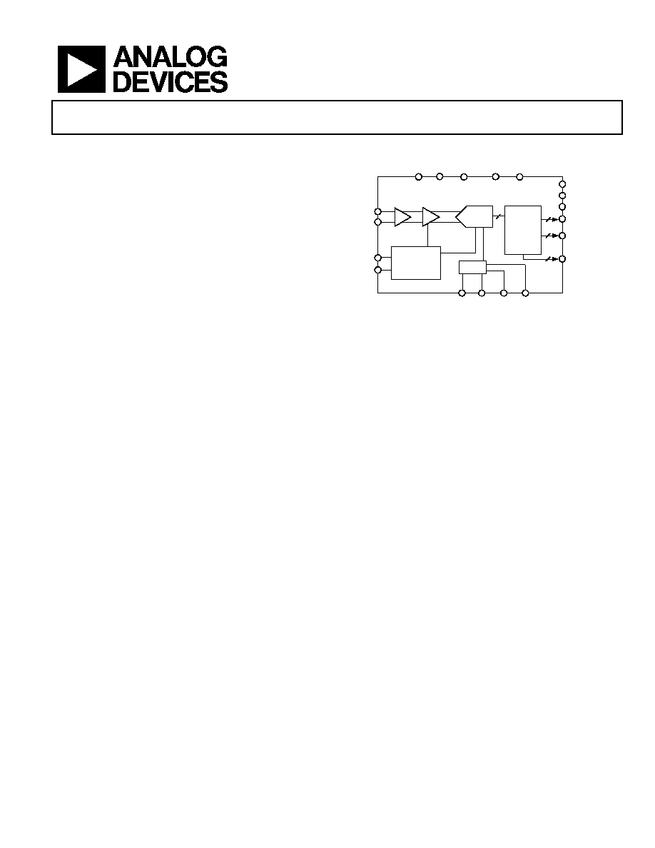
GENERAL DESCRIPTION
The AD9446 is a 16-bit, monolithic, sampling analog-to-digital
converter (ADC) with an on-chip track-and-hold circuit. It is
optimized for performance, small size, and ease of use. The
product operates up to a 100 MSPS, providing superior SNR for
instrumentation, medical imaging, and radar receivers
employing baseband (<100 MHz) IF frequencies.
The ADC requires 3.3 V and 5.0 V power supplies and a low
voltage differential input clock for full performance operation.
No external reference or driver components are required for
many applications. Data outputs are CMOS or LVDS
compatible (ANSI-644 compatible) and include the means to
reduce the overall current needed for short trace distances.
FUNCTIONAL BLOCK DIAGRAM
CMOS
OR
LVDS
OUTPUT
STAGING
CLOCK
AND TIMING
MANAGEMENT
AGND
DRGND DRVDD
VREF
CLK+
VIN+
AD9446
VIN
CLK
DCO
05490-001
AVDD1 AVDD2
DCS MODE
DFS
OUTPUT MODE
T/H
BUFFER
16
PIPELINE
ADC
2
32
2
OR
D15 TO D0
REF
REFB
SENSE REFT
Figure 1.
Optional features allow users to implement various selectable
operating conditions, including input range, data format select,
and output data mode.
The AD9446 is available in a Pb-free, 100-lead, surface-mount,
plastic package (100-lead TQFP/EP) specified over the
industrial temperature range -40°C to +85°C.
PRODUCT HIGHLIGHTS
1.
True 16-bit linearity.
2.
High performance: outstanding SNR performance for
baseband IFs in data acquisition, instrumentation,
magnetic resonance imaging, and radar receivers.
3.
Ease of use: on-chip reference and high input impedance
track-and-hold with adjustable analog input range and an
output clock simplifies data capture.
4.
Packaged in a Pb-free, 100-lead TQFP/EP package.
5.
Clock duty cycle stabilizer (DCS) maintains overall ADC
performance over a wide range of clock pulse widths.
6.
OR (out-of-range) outputs indicate when the signal is
beyond the selected input range.

AD9446
Rev. 0 | Page 2 of 36
TABLE OF CONTENTS
Features .............................................................................................. 1
Applications....................................................................................... 1
General Description ......................................................................... 1
Functional Block Diagram .............................................................. 1
Product Highlights ........................................................................... 1
Revision History ............................................................................... 2
Specifications..................................................................................... 3
DC Specifications ......................................................................... 3
AC Specifications.......................................................................... 4
Digital Specifications ................................................................... 6
Switching Specifications .............................................................. 6
Timing Diagrams.......................................................................... 7
Absolute Maximum Ratings............................................................ 8
Thermal Resistance ...................................................................... 8
ESD Caution.................................................................................. 8
Terminology .......................................................................................9
Pin Configurations and Function Descriptions ......................... 10
Equivalent Circuits......................................................................... 15
Typical Performance Characteristics ........................................... 16
Theory of Operation ...................................................................... 24
Analog Input and Reference Overview ................................... 24
Clock Input Considerations...................................................... 26
Power Considerations................................................................ 27
Digital Outputs ........................................................................... 27
Timing ......................................................................................... 27
Operational Mode Selection ..................................................... 28
Evaluation Board ............................................................................ 29
Outline Dimensions ....................................................................... 36
Ordering Guide .......................................................................... 36
REVISION HISTORY
10/05--Revision 0: Initial Version

AD9446
Rev. 0 | Page 3 of 36
SPECIFICATIONS
DC SPECIFICATIONS
AVDD1 = 3.3 V, AVDD2 = 5.0 V, DRVDD = 3.3 V, LVDS mode, specified minimum sampling rate, 3.2 V p-p differential input, internal
trimmed reference (1.6 V mode), A
IN
= -1.0 dBFS, DCS on, unless otherwise noted.
Table 1.
AD9446BSVZ-80
AD9446BSVZ-100
Parameter
Temp
Min Typ Max Min Typ Max Unit
RESOLUTION Full
16
16
Bits
ACCURACY
No Missing Codes
Full
Guaranteed
Guaranteed
Offset Error
Full
-5
±0.1
+5
-5
±0.1
+5
mV
Gain Error
Full
-3
±0.6
+3
-3
±0.5
+3
% FSR
25°C
-2
±0.3
+2
-2
±0.3
+2
%
FSR
Differential Nonlinearity (DNL)
1
Full -0.75
±0.4
+0.75
-0.85
±0.4
+0.85
LSB
Integral Nonlinearity (INL)
1
25°C
-5
±3.0
+5
-6
±3.0
+6
LSB
VOLTAGE REFERENCE
Output Voltage
1
VREF = 1.6 V (3.2 V p-p Analog Input Range)
Full
1.6
1.6
V
Load Regulation @ 1.0 mA
Full
±2
±2
mV
Reference Input Current (External 1.6 V Reference)
Full
A
INPUT REFERRED NOISE
25°C
1.5
1.9
LSB rms
ANALOG INPUT
Input Span
VREF = 1.6 V
Full
3.2
3.2
V p-p
VREF = 1.0 V (External)
Full
2.0
2.0
V p-p
Internal Input Common-Mode Voltage
Full
3.5
3.5
V
External Input Common-Mode Voltage
Full
3.2
3.8
3.2
3.8
V
Input Resistance
2
Full 1 1 k
Input Capacitance
2
Full 6 6 pF
POWER SUPPLIES
Supply Voltage
AVDD1 Full
3.14
3.3
3.46
3.14
3.3
3.46
V
AVDD2 Full
4.75
5.0
5.25
4.75
5.0
5.25
V
DRVDD--LVDS Outputs
Full
3.0
3.3
3.6
3.0
3.3
3.6
V
DRVDD--CMOS Outputs
Full
3.0
3.3
3.6
3.0
3.3
3.6
V
Supply Current
I
AVDD
1
Full 335 365
368
401
mA
I
AVDD2
1
Full 204 234
223
255
mA
I
DRVDD
1
--LVDS Outputs
Full
68
75
69
75
mA
I
DRVDD
1
--CMOS Outputs
Full
14
14
mA
PSRR
Offset Full
1
1
mV/V
Gain Full
0.2
0.2
%/V
POWER CONSUMPTION
LVDS Outputs
Full
2.4
2.6
2.6
2.8
W
CMOS Outputs (DC Input)
Full
2.2
2.3
W
1
Measured at the maximum clock rate, f
IN
= 15 MHz, full-scale sine wave, with a 100 differential termination on each pair of output bits for LVDS output mode and
approximately 5 pF loading on each output bit for CMOS output mode.
2
Input capacitance or resistance refers to the effective impedance between one differential input pin and AGND. Refer to Figure 6 for the equivalent analog input structure.

AD9446
Rev. 0 | Page 4 of 36
AC SPECIFICATIONS
AVDD1 = 3.3 V, AVDD2 = 5.0 V, DRVDD = 3.3 V, LVDS mode, specified minimum sample rate, 3.2 V p-p differential input, internal
trimmed reference (1.6 V mode), A
IN
= -1 dBFS, DCS on, unless otherwise noted.
Table 2.
AD9446BSVZ-80
AD9446BSVZ-100
Parameter
Temp
Min Typ Max Min Typ Max Unit
SIGNAL-TO-NOISE RATIO (SNR)
f
IN
= 10 MHz
25°C
79.6
81.8
78.4
79.7
dB
f
IN
= 30 MHz
25°C
80.5
81.6
78.3
79.5
dB
Full
79.2
77.9
dB
f
IN
= 70 MHz
25°C
79.0
80.6
77.7
79.0
dB
Full
78.2
77.6
dB
f
IN
= 92 MHz
25°C
80.1
78.9
dB
f
IN
= 125 MHz
25°C
78.8
78.2
dB
f
IN
= 170 MHz
25°C
77.1
77.0
dB
f
IN
= 10 MHz (2 V p-p Input)
25°C
78.3
76.6
dB
f
IN
= 30 MHz (2 V p-p Input)
25°C
78.3
76.6
dB
f
IN
= 70 MHz (2 V p-p Input)
25°C
77.6
76.2
dB
f
IN
= 92 MHz (2 V p-p Input)
25°C
77.5
76
dB
f
IN
= 125 MHz (2 V p-p Input)
25°C
76.7
75.6
dB
f
IN
= 170 MHz (2 V p-p Input)
25°C
75.5
75.1
dB
SIGNAL-TO-NOISE AND DISTORTION (SINAD)
f
IN
= 10 MHz
25°C
77.1
80.5
76.9
78.9
dB
f
IN
= 30 MHz
25°C
75.9
80.4
75.5
78.6
dB
Full
74.9
71.7
dB
f
IN
= 70 MHz
25°C
75.5
78.6
73.8
77.7
dB
Full
74.4
69.1
dB
f
IN
= 92 MHz
25°C
79.2
77.1
dB
f
IN
= 125 MHz
25°C
74.9
76.9
dB
f
IN
= 170 MHz
25°C
66.0
70.5
dB
f
IN
= 10 MHz (2 V p-p Input)
25°C
77.9
76.2
dB
f
IN
= 30 MHz (2 V p-p Input)
25°C
77.8
76.1
dB
f
IN
= 70 MHz (2 V p-p Input)
25°C
77.1
75.9
dB
f
IN
= 92 MHz (2 V p-p Input)
25°C
77.1
75.7
dB
f
IN
= 125 MHz (2 V p-p Input)
25°C
75.7
75.3
dB
f
IN
= 170 MHz (2 V p-p Input)
25°C
72.5
73.6
dB
EFFECTIVE NUMBER OF BITS (ENOB)
f
IN
= 10 MHz
25°C
13.2
13.0
Bits
f
IN
= 30 MHz
25°C
13.2
12.9
Bits
f
IN
= 70 MHz
25°C
12.9
12.8
Bits
f
IN
= 92 MHz
25°C
13.0
12.7
Bits
f
IN
= 125 MHz
25°C
12.3
12.6
Bits
f
IN
= 170 MHz
25°C
10.8
11.6
Bits

AD9446
Rev. 0 | Page 5 of 36
AD9446BSVZ-80
AD9446BSVZ-100
Parameter
Temp
Min Typ Max Min Typ Max Unit
SPURIOUS-FREE DYNAMIC RANGE
(SFDR, Second or Third Harmonic)
f
IN
= 10 MHz
25°C
82
90
82
92
dBc
f
IN
= 30 MHz
25°C
82
89
82
89
dBc
Full
80
79
dBc
f
IN
= 70 MHz
25°C
80
87
81
89
dBc
Full
79
77
dBc
f
IN
= 92 MHz
25°C
84
84
dBc
f
IN
= 125 MHz
25°C
80
83
dBc
f
IN
= 170 MHz
25°C
66
74
dBc
f
IN
= 10 MHz (2 V p-p Input)
25°C
92
94
dBc
f
IN
= 30 MHz (2 V p-p Input)
25°C
93
92
dBc
f
IN
= 70 MHz (2 V p-p Input)
25°C
92
92
dBc
f
IN
= 92 MHz (2 V p-p Input)
25°C
90
89
dBc
f
IN
= 125 MHz (2 V p-p Input)
25°C
85
87
dBc
f
IN
= 170 MHz (2 V p-p Input)
25°C
77
82
dBc
WORST SPUR EXCLUDING SECOND OR
THIRD HARMONICS
f
IN
= 10 MHz
25°C
-98
-89
-96
-91
dBc
f
IN
= 30 MHz
25°C
-97
-89
-97
-89
dBc
Full
-89
-87
dBc
f
IN
= 70 MHz
25°C
-98
-90
-96
-90
dBc
Full
-89
-88
dBc
f
IN
= 92 MHz
25°C
-98
-95
dBc
f
IN
= 125 MHz
25°C
-96
-96
dBc
f
IN
= 170 MHz
25°C
-95
-92
dBc
f
IN
= 10 MHz (2 V p-p Input)
25°C
-97
-93
dBc
f
IN
= 30 MHz (2 V p-p Input)
25°C
-97
-96
dBc
f
IN
= 70 MHz (2 V p-p Input)
25°C
-94
-94
dBc
f
IN
= 92 MHz (2 V p-p Input)
25°C
-97
-99
dBc
f
IN
= 125 MHz (2 V p-p Input)
25°C
-97
-95
dBc
f
IN
= 170 MHz (2 V p-p Input)
25°C
-93
-95
dBc
TWO-TONE SFDR
f
IN
= 10.8 MHz @ -7 dBFS,
9.8 MHz @ -7 dBFS
25°C 96
95
dBFS
f
IN
= 70.3 MHz @ -7 dBFS,
69.3 MHz @ -7 dBFS
25°C 92
92
dBFS
ANALOG BANDWIDTH
Full
325
540
MHz

AD9446
Rev. 0 | Page 6 of 36
DIGITAL SPECIFICATIONS
AVDD1 = 3.3 V, AVDD2 = 5.0 V, DRVDD = 3.3 V, R
LVDS_BIAS
= 3.74 k, unless otherwise noted.
Table 3.
AD9446BSVZ-80
AD9446BSVZ-100
Parameter
Temp
Min Typ
Max Min Typ
Max Unit
CMOS LOGIC INPUTS (DFS, DCS MODE, OUTPUT MODE)
High Level Input Voltage
Full
2.0
2.0
V
Low Level Input Voltage
Full
0.8
0.8
V
High Level Input Current
Full
200
200
A
Low Level Input Current
Full
-10
+10
-10 +10 A
Input Capacitance
Full
2
2
pF
DIGITAL OUTPUT BITS--CMOS MODE (D0 to D15, OTR)
1
DRVDD = 3.3 V
High Level Output Voltage
Full
3.25
3.25
V
Low Level Output Voltage
Full
0.2
0.2
V
DIGITAL OUTPUT BITS--LVDS MODE (D0 to D15, OTR)
V
OD
Differential Output Voltage
2
Full 247
545
247 545 mV
V
OS
Output Offset Voltage
Full
1.125
1.375
1.125
1.375 V
CLOCK INPUTS (CLK+, CLK-)
Differential Input Voltage
Full
0.2
0.2
V
Common-Mode Voltage
Full
1.3
1.5
1.6
1.3 1.5
1.6 V
Input Resistance
Full
1.1
1.4
1.7
1.1 1.4
1.7 k
Input Capacitance
Full
2
2
pF
1
Output voltage levels measured with 5 pF load on each output.
2
LVDS R
TERM
= 100 .
SWITCHING SPECIFICATIONS
AVDD1 = 3.3 V, AVDD2 = 5.0 V, DRVDD = 3.3 V, unless otherwise noted.
Table 4.
AD9446BSVZ-80
AD9446BSVZ-100
Parameter
Temp
Min Typ Max Min Typ Max Unit
CLOCK INPUT PARAMETERS
Maximum Conversion Rate
Full
80
100
MSPS
Minimum Conversion Rate
Full
1
1
MSPS
CLK Period
Full
12.5
10
ns
CLK Pulse Width High
1
(t
CLKH
) Full
5.0
4.0
ns
CLK Pulse Width Low
1
(t
CLKL
) Full
5.0
4.0
ns
DATA OUTPUT PARAMETERS
Output Propagation Delay--CMOS (t
PD
)
2
(Dx, DCO+)
Full
3.35
3.35
ns
Output Propagation Delay--LVDS (t
PD
)
3
(Dx+), (t
CPD
)
3
(DCO+) Full 2.1 3.6 4.8 2.3 3.6 4.8 ns
Pipeline Delay (Latency)
Full
13
13
Cycles
Aperture Delay (t
A
)
Full
ns
Aperture Uncertainty (Jitter, t
J
) Full
60
60
fsec
rms
1
With duty cycle stabilizer (DCS) enabled.
2
Output propagation delay is measured from clock 50% transition to data 50% transition with 5 pF load.
3
LVDS R
TERM
= 100 . Measured from the 50% point of the rising edge of CLK+ to the 50% point of the data transition.
AD9446
Rev. 0 | Page 7 of 36
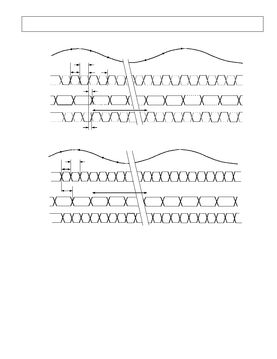
TIMING DIAGRAMS
N 13
N 12
N
N + 1
A
IN
CLK+
CLK
DATA OUT
DCO+
DCO
N
N + 1
N 1
t
CLKH
t
CLKL
1/
f
S
t
PD
13 CLOCK CYCLES
t
CPD
05490-002
Figure 2. LVDS Mode Timing Diagram
N + 1
N + 2
N 1
t
CLKL
13 CLOCK CYCLES
05490-003
N
t
CLKH
t
PD
VIN
CLK+
CLK
DX
DCO+
DCO
N 13
N 12
N 1
N
Figure 3. CMOS Timing Diagram
AD9446
Rev. 0 | Page 8 of 36
ABSOLUTE MAXIMUM RATINGS
Table 5.
Parameter
With
Respect
to
Rating
ELECTRICAL
AVDD1
AGND
-0.3 V to +4 V
AVDD2
AGND
-0.3 V to +6 V
DRVDD
DGND
-0.3 V to +4 V
AGND
DGND
-0.3 V to +0.3 V
AVDD1
DRVDD
-4 V to +4 V
AVDD2
DRVDD
-4 V to +6 V
AVDD2
AVDD1
-4 V to +6 V
D0± to D15±
DGND
0.3 V to DRVDD + 0.3 V
CLK+/CLK-
AGND
0.3 V to AVDD1 + 0.3 V
OUTPUT MODE,
DCS MODE, DFS
AGND
0.3 V to AVDD1 + 0.3 V
VIN+, VIN-
AGND
0.3 V to AVDD2 + 0.3 V
VREF
AGND
0.3 V to AVDD1 + 0.3 V
SENSE
AGND
0.3 V to AVDD1 + 0.3 V
REFT, REFB
AGND
0.3 V to AVDD1 + 0.3 V
ENVIRONMENTAL
Storage Temperature
Range
65°C to +125°C
Operating Temperature
Range
40°C to +85°C
Lead Temperature
(Soldering 10 sec)
300°C
Junction Temperature
150°C
Stresses above those listed under Absolute Maximum Ratings
may cause permanent damage to the device. This is a stress
rating only; functional operation of the device at these or any
other conditions above those indicated in the operational
section of this specification is not implied. Exposure to absolute
maximum rating conditions for extended periods may affect
device reliability.
THERMAL RESISTANCE
The heat sink of the AD9446 package must be soldered to
ground.
Table 6.
Package Type
JA
JB
JC
Unit
100-lead TQFP/EP
19.8
8.3
2
°C/W
Typical
JA
= 19.8°C/W (heat sink soldered) for multilayer
board in still air.
Typical
JB
= 8.3°C/W (heat sink soldered) for multilayer board
in still air.
Typical
JC
= 2°C/W (junction to exposed heat sink) represents
the thermal resistance through heat sink path.
Airflow increases heat dissipation, effectively reducing
JA
. Also,
more metal directly in contact with the package leads from
metal traces through holes, ground, and power planes reduces
the
JA
. It is required that the exposed heat sink be soldered to
the ground plane.
ESD CAUTION
ESD (electrostatic discharge) sensitive device. Electrostatic charges as high as 4000 V readily accumulate on
the human body and test equipment and can discharge without detection. Although this product features
proprietary ESD protection circuitry, permanent damage may occur on devices subjected to high energy
electrostatic discharges. Therefore, proper ESD precautions are recommended to avoid performance
degradation or loss of functionality.

AD9446
Rev. 0 | Page 9 of 36
TERMINOLOGY
Analog Bandwidth (Full Power Bandwidth)
The analog input frequency at which the spectral power of the
fundamental frequency (as determined by the FFT analysis) is
reduced by 3 dB.
Aperture Delay (t
A
)
The delay between the 50% point of the rising edge of the clock
and the instant at which the analog input is sampled.
Aperture Uncertainty (Jitter, t
J
)
The sample-to-sample variation in aperture delay.
Clock Pulse Width and Duty Cycle
Pulse width high is the minimum amount of time that the
clock pulse should be left in the Logic 1 state to achieve rated
performance. Pulse width low is the minimum time the clock
pulse should be left in the low state. At a given clock rate, these
specifications define an acceptable clock duty cycle.
Differential Nonlinearity (DNL, No Missing Codes)
An ideal ADC exhibits code transitions that are exactly 1 LSB
apart. DNL is the deviation from this ideal value. Guaranteed
no missing codes to 16-bit resolution indicates that all 65,536
codes must be present over all operating ranges.
Effective Number of Bits (ENOB)
The effective number of bits for a sine wave input at a given
input frequency can be calculated directly from its measured
SINAD using the following formula:
(
)
6.02
1.76
-
=
SINAD
ENOB
Gain Error
The first code transition should occur at an analog value of
½ LSB above negative full scale. The last transition should occur
at an analog value of 1½ LSB below the positive full scale. Gain
error is the deviation of the actual difference between first and
last code transitions and the ideal difference between first and
last code transitions.
Integral Nonlinearity (INL)
The deviation of each individual code from a line drawn from
negative full scale through positive full scale. The point used as
negative full scale occurs ½ LSB before the first code transition.
Positive full scale is defined as a level 1½ LSB beyond the last
code transition. The deviation is measured from the middle of
each particular code to the true straight line.
Maximum Conversion Rate
The clock rate at which parametric testing is performed.
Minimum Conversion Rate
The clock rate at which the SNR of the lowest analog signal
frequency drops by no more than 3 dB below the guaranteed
limit.
Offset Error
The major carry transition should occur for an analog value of
½ LSB below VIN+ = VIN-. Offset error is defined as the
deviation of the actual transition from that point.
Out-of-Range Recovery Time
The time it takes for the ADC to reacquire the analog input
after a transition from 10% above positive full scale to 10%
above negative full scale, or from 10% below negative full scale
to 10% below positive full scale.
Output Propagation Delay (t
PD
)
The delay between the clock rising edge and the time when all
bits are within valid logic levels.
Power-Supply Rejection Ratio
The change in full scale from the value with the supply at the
minimum limit to the value with the supply at the maximum
limit.
Signal-to-Noise and Distortion (SINAD)
The ratio of the rms input signal amplitude to the rms value of
the sum of all other spectral components below the Nyquist
frequency, including harmonics but excluding dc.
Signal-to-Noise Ratio (SNR)
The ratio of the rms input signal amplitude to the rms value of
the sum of all other spectral components below the Nyquist
frequency, excluding the first six harmonics and dc.
Spurious-Free Dynamic Range (SFDR)
The ratio of the rms signal amplitude to the rms value of the
peak spurious spectral component. The peak spurious component
may be a harmonic. SFDR can be reported in dBc (that is, degrades
as signal level is lowered) or dBFS (always related back to converter
full scale).
Temperature Drift
The temperature drift for offset error and gain error specifies
the maximum change from the initial (25°C) value to the value
at T
MIN
or T
MAX
.
Total Harmonic Distortion (THD)
The ratio of the rms input signal amplitude to the rms value of
the sum of the first six harmonic components.
Two-Tone SFDR
The ratio of the rms value of either input tone to the rms value
of the peak spurious component. The peak spurious component
may or may not be an IMD product.
AD9446
Rev. 0 | Page 10 of 36
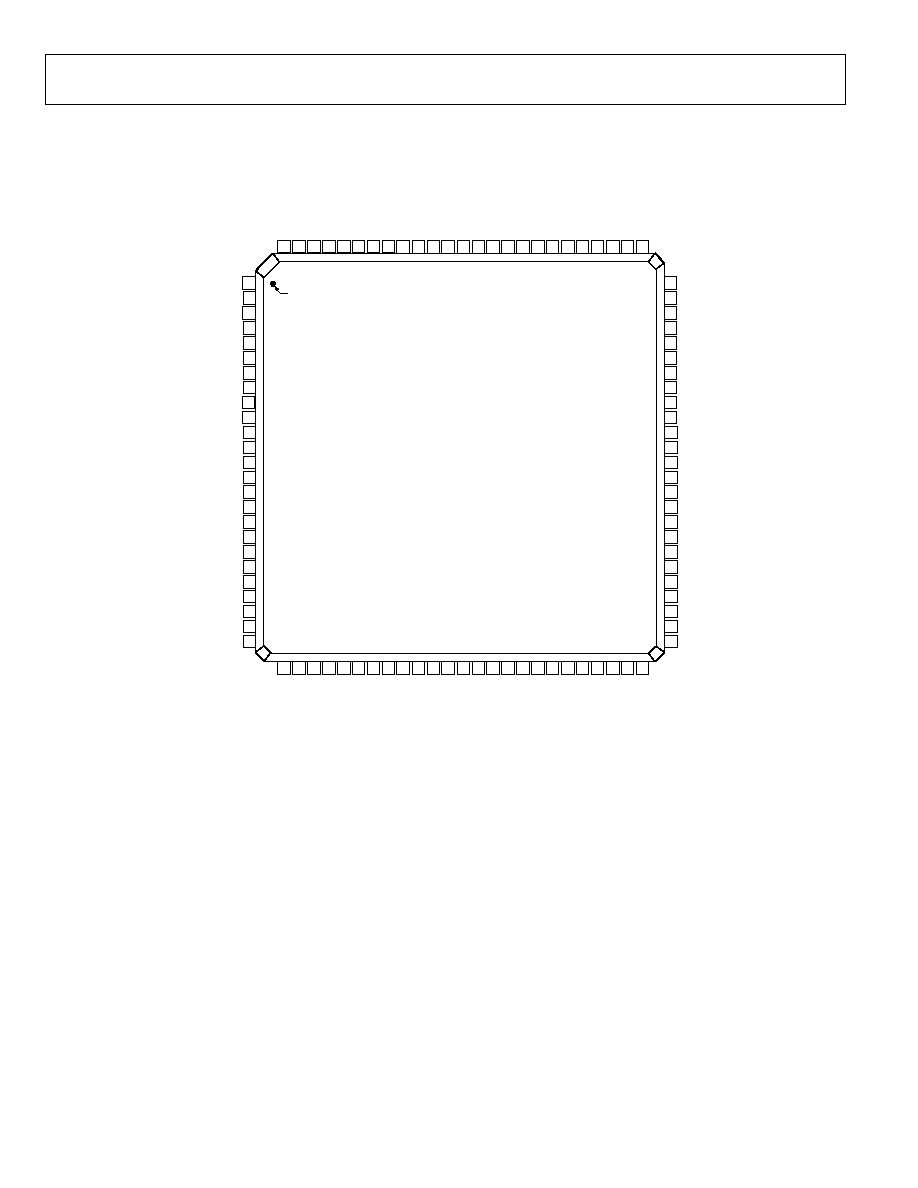
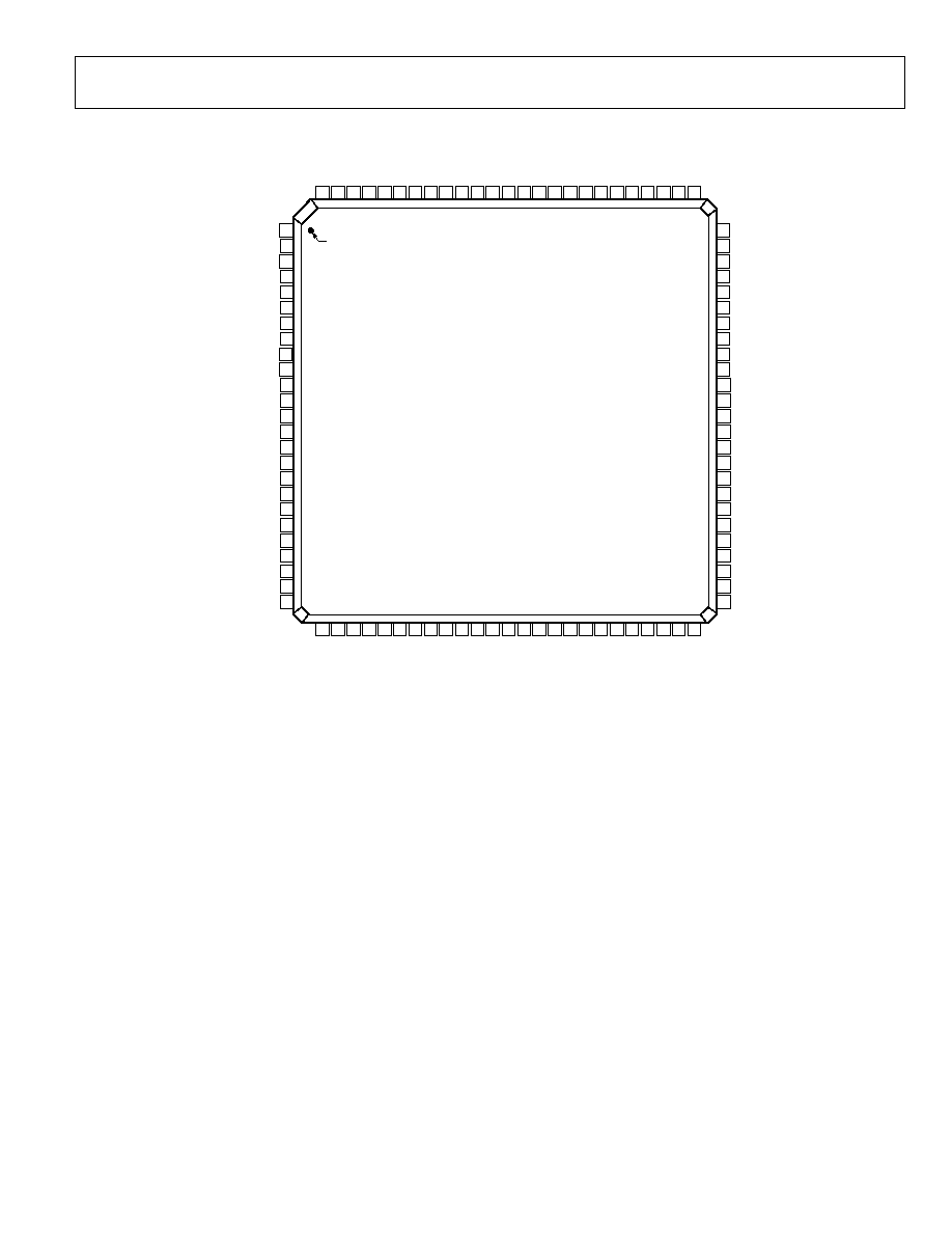
PIN CONFIGURATIONS AND FUNCTION DESCRIPTIONS
74
D10+
73
D10
72
D9+
69
D8
70
D8+
71
D9
75
DRGND
68
DCO+
67
DCO
66
D7+
64
DRVDD
63
DRGND
62
D6+
61
D6
60
D5+
59
D5
58
D4+
57
D4
56
D3+
55
D3
54
D2+
53
D2
52
D1+
51
D1
65
D7
PIN 1
DNC = DO NOT CONNECT
100
AGND
99
AGND
98
AGND
97
AV
DD1
96
AV
DD1
95
AV
DD1
94
AV
DD1
93
AV
DD1
92
AV
DD1
91
AGND
90
OR+
89
OR
88
DRV
DD
87
DRGND
86
D
15+
(
M
S
B
)
85
D1
5
84
D
14+
83
D1
4
82
D
13+
81
D1
3
80
D
12+
79
D1
2
78
D
11+
77
D1
1
76
DRV
DD
26
AV
DD2
27
AV
DD2
28
AV
DD2
29
AV
DD2
30
AV
DD2
31
AV
DD2
32
AV
DD1
33
AV
DD1
34
AV
DD1
35
AV
DD2
36
AV
DD1
37
AV
DD2
38
AV
DD1
39
AGND
40
CLK+
41
CLK
42
AGND
43
AV
DD1
44
AV
DD1
45
AV
DD1
46
AGND
47
DRGND
48
DRV
DD
49
D
0 (
L
SB
)
50
D0
+
2
DNC
3
OUTPUT MODE
4
DFS
7
SENSE
6
AVDD1
5
LVDS_BIAS
1
DCS MODE
8
VREF
9
AGND
10
REFT
12
AVDD2
13
AVDD2
14
AVDD2
15
AVDD2
16
AVDD2
17
AVDD2
18
AVDD1
19
AVDD1
20
AVDD1
21
AGND
22
VIN+
23
VIN
24
AGND
25
AVDD2
11
REFB
AD9446
LVDS MODE
TOP VIEW
(Not to Scale)
05490-004
Figure 4. 100-Lead TQFP/EP Pin Configuration in LVDS Mode
AD9446
Rev. 0 | Page 11 of 36
Table 7. Pin Function Descriptions--100-Lead TQFP/EP in LVDS Mode
Pin No.
Mnemonic
Description
1 DCS
MODE
Clock Duty Cycle Stabilizer (DCS) Control Pin. CMOS compatible. DCS = low (AGND) to enable
DCS (recommended); DCS = high (AVDD1) to disable DCS.
2
DNC
Do Not Connect. These pins should float.
3
OUTPUT
MODE
CMOS-Compatible Output Logic Mode Control Pin. OUTPUT MODE = 0 for CMOS mode;
OUTPUT MODE = 1 (AVDD1) for LVDS outputs.
4 DFS
Data Format Select Pin. CMOS control pin that determines the format of the output data. DFS =
high (AVDD1) for twos complement; DFS = low (ground) for offset binary format.
5
LVDS_BIAS
Set Pin for LVDS Output Current. Place 3.7 k resistor terminated to DRGND.
6, 18 to 20, 32 to 34, 36, 38,
43 to 45, 92 to 97
AVDD1
3.3 V (±5%) Analog Supply.
7 SENSE
Reference Mode Selection. Connect to AGND for internal 1.6 V reference (3.2 V p-p analog
input range); connect to AVDD1 for external reference.
8 VREF
1.6 V Reference I/O. Function dependent on SENSE and external programming resistors.
Decouple to ground with 0.1 F and 10 F capacitors.
9, 21, 24, 39, 42, 46, 91, 98,
99, 100, Exposed Heat Sink
AGND
Analog Ground. The exposed heat sink on the bottom of the package must be connected to
AGND.
10 REFT
Differential Reference Output. Decoupled to ground with 0.1 F capacitor and to REFB (Pin 11)
with 0.1 F and 10 F capacitors.
11 REFB
Differential Reference Output. Decoupled to ground with a 0.1 F capacitor and to REFT
(Pin 10) with 0.1 F and 10 F capacitors.
12 to 17, 25 to 31, 35, 37
AVDD2
5.0 V Analog Supply (±5%).
22 VIN+
Analog
Input--True.
23 VIN-
Analog
Input--Complement.
40 CLK+
Clock
Input--True.
41 CLK-
Clock
Input--Complement.
47, 63, 75, 87,
DRGND
Digital Output Ground.
48, 64, 76, 88
DRVDD
3.3 V Digital Output Supply (3.0 V to 3.6 V).
49
D0- (LSB)
D0 Complement Output Bit (LVDS Levels).
50
D0+
D0 True Output Bit.
51
D1-
D1 Complement Output Bit.
52 D1+
D1
True
Output
Bit.
53
D2-
D2 Complement Output Bit.
54 D2+
D2
True
Output
Bit.
55
D3-
D3 Complement Output Bit.
56 D3+
D3
True
Output
Bit.
57
D4-
D4 Complement Output Bit.
58 D4+
D4
True
Output
Bit.
59
D5-
D5 Complement Output Bit.
60 D5+
D5
True
Output
Bit.
61
D6-
D6 Complement Output Bit.
62 D6+
D6
True
Output
Bit.
65
D7-
D7 Complement Output Bit.
66 D7+
D7
True
Output
Bit.
67
DCO-
Data Clock Output--Complement.
68
DCO+
Data Clock Output--True.
69
D8-
D8 Complement Output Bit.
70 D8+
D8
True
Output
Bit.
71
D9-
D9 Complement Output Bit.
72 D9+
D9
True
Output
Bit.
73
D10-
D10 Complement Output Bit.
74
D10+
D10 True Output Bit.
77
D11-
D11 Complement Output Bit.
78
D11+
D11 True Output Bit.

AD9446
Rev. 0 | Page 12 of 36
Pin No.
Mnemonic
Description
79
D12-
D12 Complement Output Bit.
80
D12+
D12 True Output Bit.
81
D13-
D13 Complement Output Bit
82
D13+
D13 True Output Bit.
83
D14-
D14 Complement Output Bit
84
D14+
D14 True Output Bit.
85
D15-
D15 Complement Output Bit.
86
D15+ (MSB)
D15 True Output Bit.
89
OR-
Out-of-Range Complement Output Bit.
90
OR+
Out-of-Range True Output Bit.
AD9446
Rev. 0 | Page 13 of 36
74
D4+
73
D3+
72
D2+
69
DNC
70
D0+ (LSB)
71
D1+
75
DRGND
68
DCO+
67
DCO
66
DNC
64
DRVDD
63
DRGND
62
DNC
61
DNC
60
DNC
59
DNC
58
DNC
57
DNC
56
DNC
55
DNC
54
DNC
53
DNC
52
DNC
51
DNC
65
DNC
PIN 1
DNC = DO NOT CONNECT
100
AGND
99
AGND
98
AGND
97
AV
DD1
96
AV
DD1
95
AV
DD1
94
AV
DD1
93
AV
DD1
92
AV
DD1
91
AGND
90
OR+
89
D
15+
(
M
SB
)
88
DRV
DD
87
DRGND
86
D
14+
85
D
13+
84
D
12+
83
D
11+
82
D
10+
81
D9
+
80
D8
+
79
D7
+
78
D6
+
77
D5
+
76
DRV
DD
26
AV
DD2
27
AV
DD2
28
AV
DD2
29
AV
DD2
30
AV
DD2
31
AV
DD2
32
AV
DD1
33
AV
DD1
34
AV
DD1
35
AV
DD2
36
AV
DD1
37
AV
DD2
38
AV
DD1
39
AGND
40
CLK+
41
CLK
42
AGND
43
AV
DD1
44
AV
DD1
45
AV
DD1
46
AGND
47
DRGND
48
DRV
DD
49
DNC
50
DNC
2
DNC
3
OUTPUT MODE
4
DFS
7
SENSE
6
AVDD1
5
LVDS_BIAS
1
DCS MODE
8
VREF
9
AGND
10
REFT
12
AVDD2
13
AVDD2
14
AVDD2
15
AVDD2
16
AVDD2
17
AVDD2
18
AVDD1
19
AVDD1
20
AVDD1
21
AGND
22
VIN+
23
VIN
24
AGND
25
AVDD2
11
REFB
AD9446
CMOS MODE
TOP VIEW
(Not to Scale)
05490-005
Figure 5. 100-Lead TQFP/EP Pin Configuration in CMOS Mode

AD9446
Rev. 0 | Page 14 of 36
Table 8. Pin Function Descriptions--100-Lead TQFP/EP in CMOS Mode
Pin No.
Mnemonic
Description
1 DCS
MODE
Clock Duty Cycle Stabilizer (DCS) Control Pin. CMOS compatible. DCS = low (AGND) to
enable DCS (recommended); DCS = high (AVDD1) to disable DCS.
2, 49 to 62, 65 to 66, 69,
DNC
Do Not Connect. These pins should float.
3 OUTPUT
MODE
CMOS-Compatible Output Logic Mode Control Pin. OUTPUT MODE = 0 for CMOS mode;
OUTPUT MODE = 1 (AVDD1) for LVDS outputs.
4 DFS
Data Format Select Pin. CMOS control pin that determines the format of the output data.
DFS = high (AVDD1) for twos complement; DFS = low (ground) for offset binary format.
5
LVDS_BIAS
Set Pin for LVDS Output Current. Place 3.7 k resistor terminated to DRGND.
6, 18 to 20, 32 to 34, 36,
38, 43 to 45, 92 to 97
AVDD1
3.3 V (±5%) Analog Supply.
7 SENSE
Reference Mode Selection. Connect to AGND for internal 1 V reference; connect to AVDD1
for external reference.
8 VREF
1.6 V Reference I/O. Function dependent on SENSE and external programming resistors.
Decouple to ground with 0.1 F and 10 F capacitors.
9, 21, 24, 39, 42, 46, 91, 98,
99, 100, Exposed Heat
Sink
AGND
Analog Ground. The exposed heat sink on the bottom of the package must be connected to
AGND.
10 REFT
Differential Reference Output. Decoupled to ground with 0.1 F capacitor and to REFB (Pin 11)
with 0.1 F and 10 F capacitors.
11 REFB
Differential Reference Output. Decoupled to ground with a 0.1 F capacitor and to REFT (Pin 10)
with 0.1 F and 10 F capacitors.
12 to 17, 25 to 31, 35, 37
AVDD2
5.0 V Analog Supply (±5%).
22 VIN+
Analog
Input--True.
23 VIN-
Analog
Input--Complement.
40 CLK+
Clock
Input--True.
41 CLK-
Clock
Input--Complement.
47, 63, 75, 87,
DRGND
Digital Output Ground.
48, 64, 76, 88
DRVDD
3.3 V Digital Output Supply (3.0 V to 3.6 V).
67
DCO-
Data Clock Output--Complement.
68
DCO+
Data Clock Output--True.
70
D0+ (LSB)
D0 True Output Bit (CMOS levels).
71 D1+
D1
True
Output
Bit.
72 D2+
D2
True
Output
Bit.
73 D3+
D3
True
Output
Bit.
74 D4+
D4
True
Output
Bit.
77 D5+
D5
True
Output
Bit.
78 D6+
D6
True
Output
Bit.
79 D7+
D7
True
Output
Bit.
80 D8+
D8
True
Output
Bit.
81 D9+
D9
True
Output
Bit.
82
D10+
D10 True Output Bit.
83
D11+
D11 True Output Bit.
84
D12+
D12 True Output Bit.
85
D13+
D13 True Output Bit.
86
D14+
D14 True Output Bit.
89
D15+ (MSB)
D15 True Output Bit.
90
OR+
Out-of-Range True Output Bit.
AD9446
Rev. 0 | Page 15 of 36
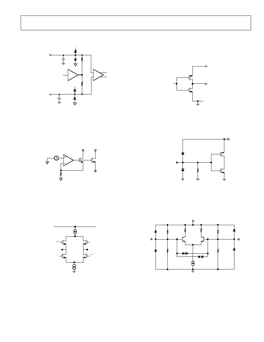
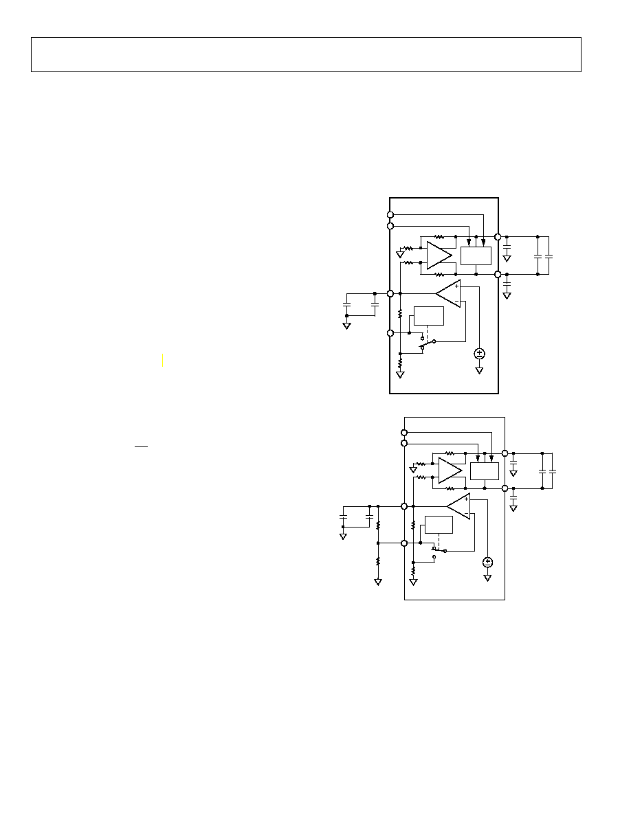
EQUIVALENT CIRCUITS
X1
3.5V
1k
1k
AVDD2
VIN+
VIN
T/H
AVDD2
05490-006
6pF
6pF
Figure 6. Equivalent Analog Input Circuit
05490-007
1.2V
DRVDD
DRVDD
K
3.74k
I
LVDSOUT
LVDSBIAS
Figure 7. Equivalent LVDS_BIAS Circuit
DRVDD
DX
DX+
V
V
V
V
05490-008
Figure 8. Equivalent LVDS Digital Output Circuit
DX
DRVDD
05490-009
Figure 9. Equivalent CMOS Digital Output Circuit
DCS MODE,
OUTPUT MODE,
DFS
VDD
30k
05490-010
Figure 10. Equivalent Digital Input Circuit,
DFS, DCS MODE, OUTPUT MODE
CLK+
3k
2.5k
3k
2.5k
AVDD2
CLK
05490-011
Figure 11. Equivalent Sample Clock Input Circuit
AD9446
Rev. 0 | Page 16 of 36
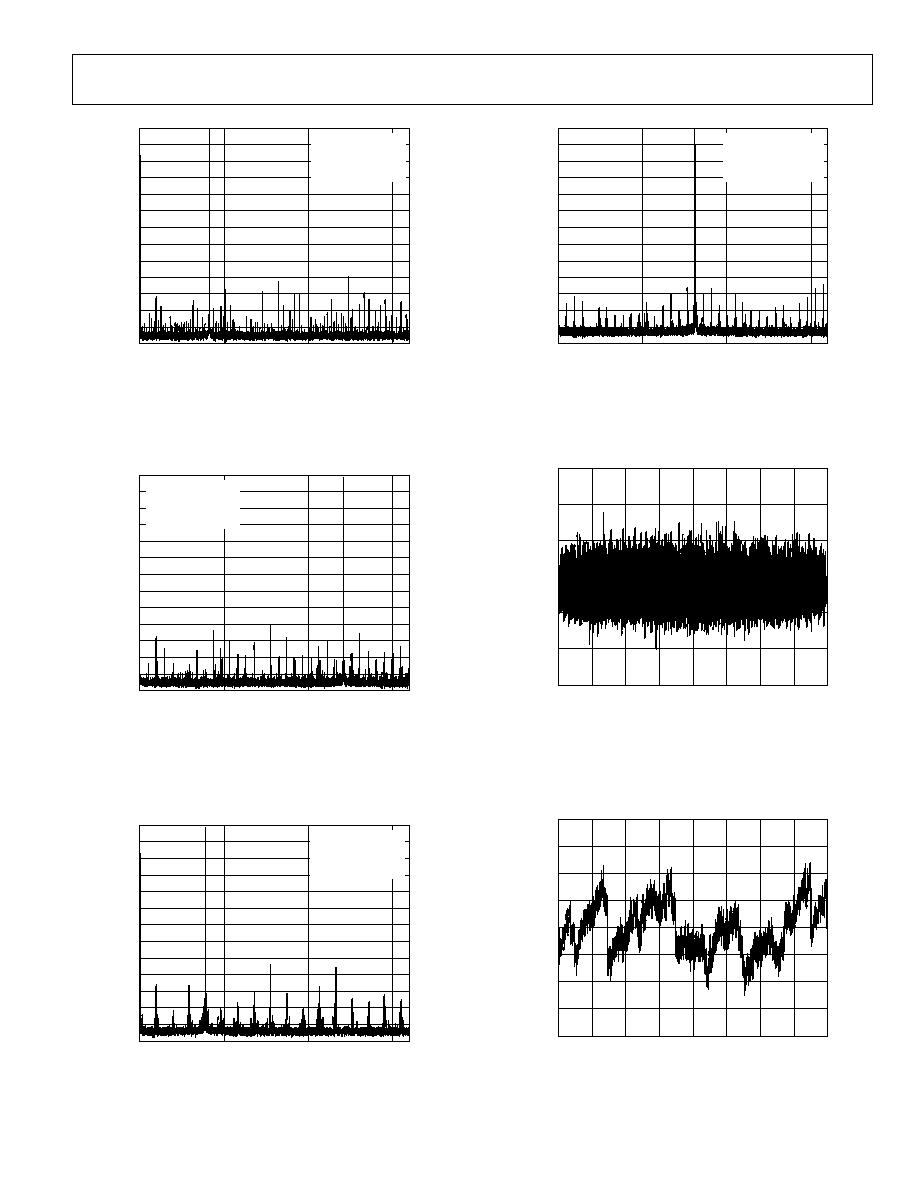
TYPICAL PERFORMANCE CHARACTERISTICS
AVDD1 = 3.3 V, AVDD2 = 5.0 V, DRVDD = 3.3 V, rated sample rate, LVDS mode, DCS enabled, T
A
= 25°C, 3.2 V p-p differential
input, AIN = -1dBFS, internal trimmed reference (nominal VREF = 1.6 V), unless otherwise noted.
0
130
0
50.0
05490-012
FREQUENCY (MHz)
AMP
LITUDE
(dBFS
)
100MSPS
10.3MHz @ 1.0dBFS
SNR = 79.7dB
ENOB = 13.1BITS
SFDR = 90dBc
10
20
30
40
50
60
70
80
90
100
110
120
12.5
25.0
37.5
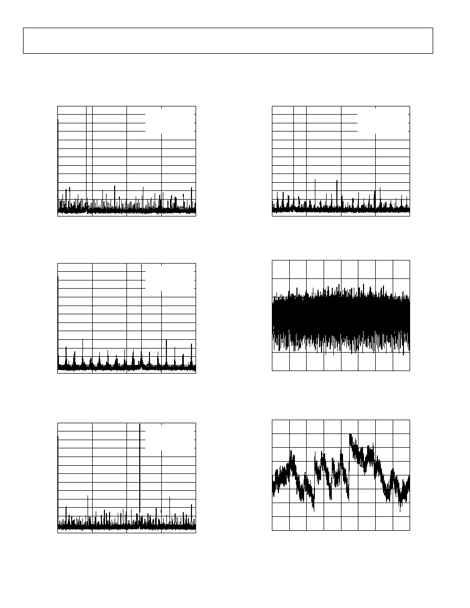
Figure 12. AD9446-100 64k Point Single-Tone FFT/100 MSPS/10.3 MHz
0
130
0
50.0
05490-013
FREQUENCY (MHz)
AMP
LITUDE
(dBFS
)
100MSPS
30.3MHz @ 1.0dBFS
SNR = 79.5dB
ENOB = 12.9BITS
SFDR = 90dBc
10
20
30
40
50
60
70
80
90
100
110
120
12.5
25.0
37.5
Figure 13. AD9446-100 64k Point Single-Tone FFT/100 MSPS/30.3 MHz
0
130
0
50.0
05490-014
FREQUENCY (MHz)
AMP
LITUDE
(dBFS
)
100MSPS
70.3MHz @ 1.0dBFS
SNR = 79.0dB
ENOB = 12.9BITS
SFDR = 86dBc
10
20
30
40
50
60
70
80
90
100
110
120
12.5
25.0
37.5
Figure 14. AD9446-100 64k Point Single-Tone FFT/100 MSPS/70.3 MHz
0
130
0
50.0
05490-015
FREQUENCY (MHz)
AMP
LITUDE
(dBFS
)
100MSPS
92.16MHz @ 1.0dBFS
SNR = 78.9dB
ENOB = 12.7BITS
SFDR = 84dBc
10
20
30
40
50
60
70
80
90
100
110
120
12.5
25.0
37.5
Figure 15. AD9446-100 64k Point Single-Tone FFT/100 MSPS/92.16 MHz
0.6
0.6
0
05490-016
OUTPUT CODE
DNL E
RROR (MS
B
)
0
65536
8192
16384 24576 32768 40960 49152 57344
0.4
0.2
0
0.2
0.4
Figure 16. AD9446-100 DNL Error vs. Output Code, 100 MSPS, 10.3 MHz
4
4
0
05490-017
OUTPUT CODE
INL E
RROR (MS
B
)
0
65536
8192
16384 24576 32768 40960 49152 57344
3
2
1
0
1
2
3
Figure 17. AD9446-100 INL Error vs. Output Code, 100 MSPS, 10.3 MHz
AD9446
Rev. 0 | Page 17 of 36
0
130
0
05490-018
FREQUENCY (MHz)
AMP
LITUDE
(dBFS
)
80MSPS
10.3MHz @ 1.0dBFS
SNR = 81.8dB
ENOB = 13.2BITS
SFDR = 90dBc
10
20
30
40
50
60
70
80
90
100
110
120
12.5
25.0
37.5
Figure 18. AD9446-80 64k Point Single-Tone FFT/80 MSPS/10.3 MHz
0
130
0
05490-019
FREQUENCY (MHz)
AMP
LITUDE
(dBFS
)
80MSPS
30.3MHz @ 1.0dBFS
SNR = 81.6dB
ENOB = 13.2BITS
SFDR = 89dBc
10
20
30
40
50
60
70
80
90
100
110
120
12.5
25.0
37.5
Figure 19. AD9446-80 64k Point Single-Tone FFT/80 MSPS/30.3 MHz
0
130
0
05490-020
FREQUENCY (MHz)
AMP
LITUDE
(dBFS
)
80MSPS
70.3MHz @ 1.0dBFS
SNR = 80.6dB
ENOB = 12.9BITS
SFDR = 85dBc
10
20
30
40
50
60
70
80
90
100
110
120
12.5
25.0
37.5
Figure 20. AD9446-80 64k Point Single-Tone FFT/80 MSPS/70.3 MHz
0
130
0
05490-021
FREQUENCY (MHz)
AMP
LITUDE
(dBFS
)
80MSPS
100.3MHz @ 1.0dBFS
SNR = 79.5dB
ENOB = 12.7BITS
SFDR = 92dBc
10
20
30
40
50
60
70
80
90
100
110
120
12.5
25.0
37.5
Figure 21. AD9446-80 64k Point Single-Tone FFT/80 MSPS/100.3 MHz
0.6
0.6
0
05490-022
OUTPUT CODE
DNL E
RROR (MS
B
)
0
65536
8192
16384 24576 32768 40960 49152 57344
0.4
0.2
0
0.2
0.4
Figure 22. AD9446-80 DNL Error vs. Output Code, 80 MSPS, 10.3 MHz
4
4
0
05490-023
OUTPUT CODE
INL E
RROR (MS
B
)
0
65536
8192
16384 24576 32768 40960 49152 57344
3
2
1
0
1
2
3
Figure 23. AD9446-80 INL Error vs. Output Code, 80 MSPS, 10.3 MHz
AD9446
Rev. 0 | Page 18 of 36
95
70
0
180
05490-024
ANALOG INPUT FREQUENCY (MHz)
(dB)
20
40
60
80
100
120
140
160
90
85
80
75
SFDR (dBc) +85°C
SFDR (dBc) 40°C
SNR (dB) +25°C
SNR (dB) +85°C
SNR (dB) 40°C
SFDR (dBc) +25°C
Figure 24. AD9446-100 SNR/SFDR vs. Analog Input Frequency, 100 MSPS, 3.2 V p-p
95
70
0
180
05490-025
ANALOG INPUT FREQUENCY (MHz)
(dB)
20
40
60
80
100
120
140
160
90
85
80
75
SFDR (dBc) +85°C
SFDR (dBc) 40°C
SNR (dB) +25°C
SNR (dB) +85°C
SNR (dB) 40°C
SFDR (dBc) +25°C
Figure 25. AD9446-100 SNR/SFDR vs. Analog Input Frequency, 100 MSPS,
3.2 V p-p, CMOS Output Mode
120
0
100
0
05490-026
ANALOG INPUT AMPLITUDE (dB)
(dB)
100
80
60
40
20
90
80
70
60
50
40
30
20
10
SNR dB
SNR dBFS
SFDR dBc
SFDR dBFS
Figure 26. AD9446-100 SNR/SFDR vs. Analog Input Level, 100 MSPS
95
70
0
180
05490-027
ANALOG INPUT FREQUENCY (MHz)
(dB)
20
40
60
80
100
120
140
160
90
85
80
75
SFDR (dBc) +85°C
SFDR (dBc) 40°C
SNR (dB) +25°C
SNR (dB) +85°C
SNR (dB) 40°C
SFDR (dBc) +25°C
Figure 27. AD9446-100 SNR/SFDR vs. Analog Input Frequency, 100 MSPS, 2.0 V p-p
86
77
78
1.8
4.2
05490-039
ANALOG INPUT RANGE (V p-p)
(dB)
85
84
83
81
82
80
79
2.0 2.2 2.4 2.6 2.8 3.0 3.2 3.4 3.6 3.8 4.0
80M SNR dBFS
100M SNR dBFS
Figure 28. AD9446-100 SNR vs. Input Range, 30.3 MHz, -30 dBFS
130
0
100
0
05490-029
ANALOG INPUT AMPLITUDE (dB)
(dB)
90
80
70
60
50
40
30
20
10
SNR dB
SNR dBFS
SFDR dBc
SFDR dBFS
110
90
70
50
30
10
Figure 29. AD9446-100 SNR/SFDR vs. Analog Input Level, 100 MSPS,
CMOS Output Mode
AD9446
Rev. 0 | Page 19 of 36
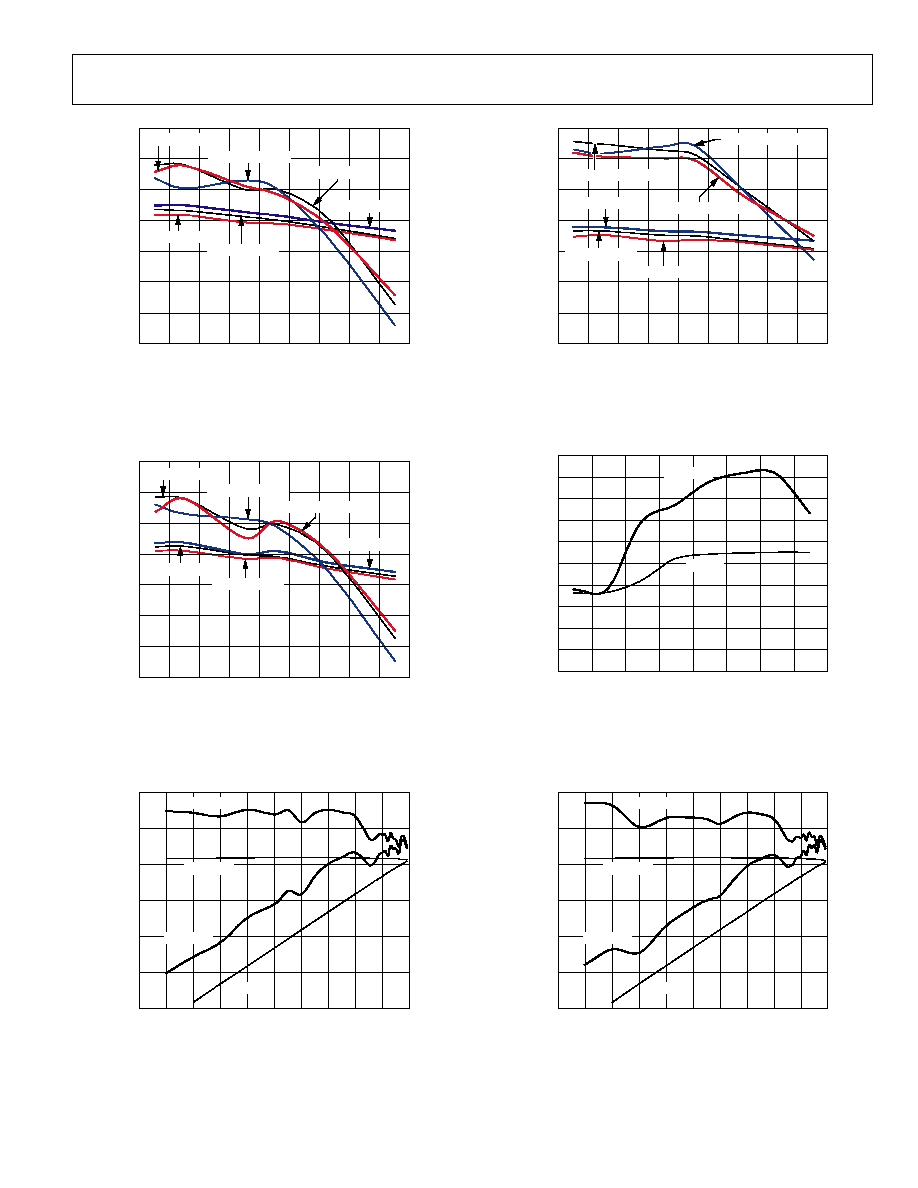
95
60
0
180
05490-030
ANALOG INPUT FREQUENCY (MHz)
(dB)
20
40
60
80
100
120
140
160
90
85
80
75
70
65
SFDR (dBc) +85°C
SFDR (dBc) 40°C
SNR (dB) +25°C
SNR (dB) +85°C
SNR (dB) 40°C
SFDR (dBc) +25°C
Figure 30. AD9446-80 SNR/SFDR vs. Analog Input Frequency, 80 MSPS, 3.2 V p-p
95
60
0
180
05490-031
ANALOG INPUT FREQUENCY (MHz)
(dB)
20
40
60
80
100
120
140
160
90
85
80
75
70
65
SFDR (dBc) +85°C
SFDR (dBc) 40°C
SNR (dB) +25°C
SNR (dB) +85°C
SNR (dB) 40°C
SFDR (dBc) +25°C
Figure 31. AD9446-80 SNR/SFDR vs. Analog Input Frequency, 80 MSPS, 3.2 V p-p,
CMOS Mode
120
0
100
0
05490-032
ANALOG INPUT AMPLITUDE (dB)
(dB)
100
80
60
40
20
90
80
70
60
50
40
30
20
10
SNR dB
SNR dBFS
SFDR dBc
SFDR dBFS
Figure 32. AD9446-80 SNR/SFDR vs. Analog Input Level, 80 MSPS
95
60
0
180
05490-033
ANALOG INPUT FREQUENCY (MHz)
(dB)
20
40
60
80
100
120
140
160
90
85
80
75
70
65
SFDR (dBc) +85°C
SFDR (dBc) 40°C
SNR (dB) +25°C
SNR (dB) +85°C
SNR (dB) 40°C
SFDR (dBc) +25°C
Figure 33. AD9446-80 SNR/SFDR vs. Analog Input Frequency, 80 MSPS, 2.0 V p-p
90
70
72
2.6
2.8
3.0
3.2
3.4
3.6
3.8
4.0
4.2
05490-034
ANALOG INPUT COMMON-MODE VOLTAGE
(dB)
SNR dB
SFDR dBc
88
86
82
84
80
78
76
74
Figure 34. AD9446-80 SNR/SFDR vs. Analog Input Common Mode, 80 MSPS
120
0
100
0
05490-035
ANALOG INPUT AMPLITUDE (dB)
(dB)
100
80
60
40
20
90
80
70
60
50
40
30
20
10
SNR dB
SNR dBFS
SFDR dBc
SFDR dBFS
Figure 35. AD9446-80 SNR/SFDR vs. Analog Input Level, 80 MSPS,
CMOS Output Mode
AD9446
Rev. 0 | Page 20 of 36
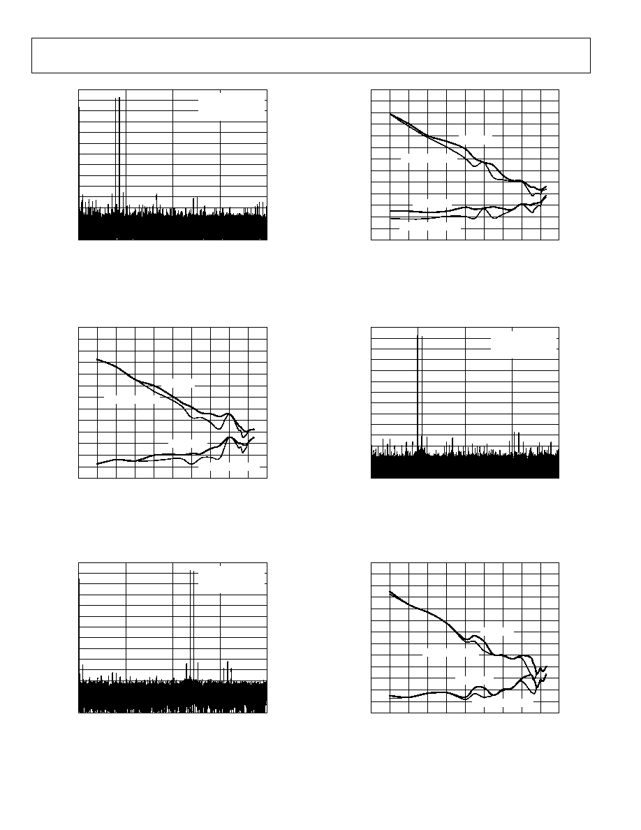
0
140
0
50.0
05490-037
FREQUENCY (MHz)
AMP
LITUDE
(dBFS
)
100MSPS
9.8MHz @ 7.0dBFS
10.8MHz @ 7.0dBFS
SFDR = 95dBc
12.5
25.0
37.5
10
20
30
40
50
60
70
80
90
100
110
120
130
Figure 36. AD9446-100 64k Point Two-Tone FFT/100 MSPS/9.8 MHz, 10.8 MHz
0
130
100
0
05490-038
FUNDAMENTAL LEVEL (dB)
S
P
UR AND IMD3
(dB)
90
80
70
60
50
40
30
20
10
SFDR dBFS
SFDR dBc
WORST IMD3 dBc
WORST IMD3 dBFS
10
20
30
40
50
60
70
80
90
100
110
120
Figure 37. AD9446-100 Two-Tone SFDR vs. Analog Input Level 100 MSPS/
9.8 MHz, 10.8 MHz
0
140
0
50.0
05490-040
FREQUENCY (MHz)
AMP
LITUDE
(dBFS
)
100MSPS
69.3MHz @ 7.0dBFS
70.3MHz @ 7.0dBFS
SFDR = 92dBc
12.5
25.0
37.5
10
20
30
40
50
60
70
80
90
100
110
120
130
Figure 38. AD9446-100 64k Point Two-Tone FFT/100 MSPS/69.3 MHz, 70.3 MHz
0
130
100
0
05490-041
FUNDAMENTAL LEVEL (dB)
S
P
UR AND IMD3
(dB)
90
80
70
60
50
40
30
20
10
SFDR dBFS
SFDR dBc
WORST IMD3 dBc
WORST IMD3 dBFS
10
20
30
40
50
60
70
80
90
100
110
120
Figure 39. AD9446-100 Two-Tone SFDR vs. Analog Input Level 100 MSPS/
69.3 MHz, 70.3 MHz
0
140
0
4
05490-042
FREQUENCY (MHz)
AMP
LITUDE
(dBFS
)
0
80MSPS
9.8MHz @ 7.0dBFS
10.8MHz @ 7.0dBFS
SFDR = 96dBc
10
20
30
10
20
30
40
50
60
70
80
90
100
110
120
130
Figure 40. AD9446-80 64k Point Two-Tone FFT/80 MSPS/9.8 MHz, 10.8 MHz
0
130
100
0
05490-043
FUNDAMENTAL LEVEL (dB)
S
P
UR AND IMD3
(dB)
90
80
70
60
50
40
30
20
10
SFDR dBFS
SFDR dBc
WORST IMD3 dBc
WORST IMD3 dBFS
10
20
30
40
50
60
70
80
90
100
110
120
Figure 41. AD9446-80 Two-Tone SFDR vs. Analog Input Level 80 MSPS/
9.8 MHz, 10.8 MHz
AD9446
Rev. 0 | Page 21 of 36
16000
0
05490-044
OUTPUT CODE
FRE
Q
UE
NCY
N + 7
N + 6
N + 5
N + 4
N + 3
N + 2
N + 1
N
N
1
N
2
N
3
N
4
N
5
N
6
N
7
11 40 315
426
22
80
SAMPLE SIZE = 65538
14000
12000
10000
8000
6000
4000
2000
1192
3424
7277
8376
4073
1458
11927
12619
14296
Figure 42. AD9446-100 Grounded Input Histogram
0
140
0
40
05490-045
FREQUENCY (MHz)
AMP
LITUDE
(dBFS
)
80MSPS
69.3MHz @ 7.0dBFS
70.3MHz @ 7.0dBFS
SFDR = 92dBc
10
20
30
10
20
30
40
50
60
70
80
90
100
110
120
130
Figure 43. AD9446-80 64k Point Two-Tone FFT/80 MSPS/69.3 MHz, 70.3 MHz
0
130
100
0
05490-046
FUNDAMENTAL LEVEL (dB)
S
P
UR AND IMD3
(dB)
90
80
70
60
50
40
30
20
10
SFDR dBFS
SFDR dBc
WORST IMD3 dBc
WORST IMD3 dBFS
10
20
30
40
50
60
70
80
90
100
110
120
Figure 44. AD9446-80 Two-Tone SFDR vs. Analog Input Level 80 MSPS/
69.3 MHz, 70.3 MHz
18000
0
05490-047
OUTPUT CODE
FRE
Q
UE
NCY
N + 6
N + 5
N + 4
N + 3
N + 2
N + 1
N
N
1
N
2
N
3
N
4
N
5
N
6
3
10 146
947
30
198
SAMPLE SIZE = 65538
16000
14000
12000
10000
8000
6000
4000
2000
3916
4393
10145
11027
17090
16450
1181
Figure 45. AD9446-80 Grounded Input Histogram
0
0.8
40
05490-048
TEMPERATURE (°C)
GAIN E
RROR (%FS
R)
0.1
0.2
0.3
0.4
0.5
0.6
0.7
20
0
20
40
60
80
Figure 46. AD9446-100 Gain vs. Temperature
400
0
0
05490-049
SAMPLE RATE (MSPS)
I
SU
PPLY
(mA)
140
350
300
250
200
150
100
50
20
40
60
80
100
120
DRVDD
AVDD2
AVDD1
Figure 47. AD9446-80 Power Supply Current vs. Sample Rate
10.3 MHz @ -1 dBFS
AD9446
Rev. 0 | Page 22 of 36
95
79
1.8
05490-050
ANALOG INPUT RANGE (V p-p)
(dB)
4.2
2.0 2.2 2.4 2.6 2.8 3.0 3.2 3.4 3.6 3.8 4.0
10.3MHz SFDR dBc
30.3MHz SFDR dBc
93
91
89
87
85
83
81
70.3MHz SFDR dBc
Figure 48. AD9446-100/SFDR vs. Analog Input Range,
100 MSPS
1.625
1.620
1.615
1.610
1.605
40
05490-051
TEMPERATURE (°C)
VR
EF
20
0
20
40
60
80
Figure 49. AD9446-100 VREF vs. Temperature
450
400
0
0
05490-063
SAMPLE RATE (MSPS)
I
SU
PPLY
(mA)
140
350
300
250
200
150
100
50
20
40
60
80
100
120
DRVDD
AVDD2
AVDD1
Figure 50. AD9446-100 Power Supply Current vs. Sample Rate
10.3 MHz @ -1 dBFS
82
76
1.8
05490-064
ANALOG INPUT RANGE (V p-p)
(dB)
4.2
2.0 2.2 2.4 2.6 2.8 3.0 3.2 3.4 3.6 3.8 4.0
10.3MHz SFDR dBc
30.3MHz SFDR dBc
81
80
79
78
77
70.3MHz SFDR dBc
Figure 51. AD9446-100 SNR vs. Analog Input Range,
100 MSPS
95
79
1.8
05490-065
ANALOG INPUT RANGE (V p-p)
(dB)
4.2
2.0 2.2 2.4 2.6 2.8 3.0 3.2 3.4 3.6 3.8 4.0
10.3MHz SFDR dBc
30.3MHz SFDR dBc
93
91
89
87
85
83
81
70.3MHz SFDR dBc
Figure 52. AD9446-80 SFDR vs. Analog Input Range,
100 MSPS
84
77
1.8
05490-066
ANALOG INPUT RANGE (V p-p)
(dB)
4.2
10.3MHz SNR dB
30.3MHz SNR dB
70.3MHz SNR dB
83
82
81
80
79
78
2.0 2.2 2.4 2.6 2.8 3.0 3.2 3.4 3.6 3.8 4.0
Figure 53. AD9446-80/SNR vs. Analog Input Range,
80 MSPS
AD9446
Rev. 0 | Page 23 of 36
100
75
0
05490-036
SAMPLE RATE (MSPS)
(dB)
95
90
85
80
20
10
30
40
50
60
70
80
90
100 110
80M SFDR dBc
100M SFDR dBc
100M SNR dB
80M SNR dB
Figure 54. AD9446 Single-Tone SNR/SFDR vs. Sample Rate 2.3 MHz
AD9446
Rev. 0 | Page 24 of 36
THEORY OF OPERATION
The AD9446 architecture is optimized for high speed and ease
of use. The analog inputs drive an integrated, high bandwidth
track-and-hold circuit that samples the signal prior to quantization
by the 16-bit pipeline ADC core. The device includes an on-board
reference and input logic that accepts TTL, CMOS, or LVPECL
levels. The digital output logic levels are user selectable as standard
3 V CMOS or LVDS (ANSI-644 compatible) via the OUTPUT
MODE pin.
ANALOG INPUT AND REFERENCE OVERVIEW
A stable and accurate 0.5 V band gap voltage reference is built
into the AD9446. The input range can be adjusted by varying
the reference voltage applied to the AD9446, using either the
internal reference or an externally applied reference voltage.
The input span of the ADC tracks reference voltage changes
linearly.
Internal Reference Connection
A comparator within the AD9446 detects the potential at the
SENSE pin and configures the reference into three possible states,
which are summarized in Table 9. If SENSE is grounded, the
reference amplifier switch is connected to the internal resistor
divider (see Figure 55), setting VREF to ~1.6 V. If a resistor
divider is connected as shown in Figure 56, the switch again sets
to the SENSE pin. This puts the reference amplifier in a
noninverting mode with the VREF output defined as
+
×
=
R1
R2
V
VREF
1
5
.
0
In all reference configurations, REFT and REFB drive the
analog-to-digital conversion core and establish its input span.
The input range of the ADC always equals twice the voltage at
the reference pin for either an internal or an external reference.
Internal Reference Trim
The internal reference voltage is trimmed during the production
test; therefore, there is little advantage to the user supplying an
external voltage reference to the AD9446. The gain trim is per-
formed with the AD9446 input range set to 3.2 V p-p nominal
(SENSE connected to AGND). Because of this trim and the
maximum ac performance provided by the 3.2 V p-p analog
input range, there is little benefit to using analog input ranges
<2 V p-p. However, reducing the range can improve SFDR
performance in some applications. Likewise, increasing the
range up to 3.8 V p-p can improve SNR. Users are cautioned
that the differential nonlinearity of the ADC varies with the
reference voltage. Configurations that use <2.0 V p-p may
exhibit missing codes and therefore degraded noise and
distortion performance.
10
F
+
0.1
F
VREF
SENSE
0.5V
AD9446
VIN
VIN+
REFT
0.1
F
0.1
F
10
F
0.1
F
REFB
SELECT
LOGIC
ADC
CORE
+
05490-052
Figure 55. Internal Reference Configuration
05490-053
10
F
+
0.1
F
VREF
SENSE
R2
R1
0.5V
AD9446
VIN
VIN+
REFT
0.1
F
0.1
F
10
F
0.1
F
REFB
SELECT
LOGIC
ADC
CORE
+
Figure 56. Programmable Reference Configuration
AD9446
Rev. 0 | Page 25 of 36
Table 9. Reference Configuration Summary
Selected Mode
SENSE Voltage
Resulting VREF (V)
Resulting Differential Span (V p-p)
External Reference
AVDD
N/A
2 × external reference
Programmable Reference
0.2 V to VREF
+
×
R1
R2
1
0.5
(See Figure 56)
2 × VREF
Programmable Reference
(Set for 2 V p-p)
0.2 V to VREF
+
×
R1
R2
1
0.5
, R1 = R2 = 1 k
2.0
Programmable Reference
(Set for 2 V p-p)
0.2 V to VREF
+
×
R1
R2
1
0.5
, R1 = 1 k , R2 = 2.8 k
3.8
Internal Fixed Reference
AGND to 0.2 V
1.6
3.2
External Reference Operation
When the SENSE pin is tied to AVDD, the internal reference is
disabled, allowing the use of an external reference. An internal
reference buffer loads the external reference with an equivalent
7 k load. The internal buffer still generates the positive and
negative full-scale references, REFT and REFB, for the ADC
core. The input span is always twice the value of the reference
voltage; therefore, the external reference must be limited to a
maximum of 2.0 V. See Figure 46 for gain variation vs.
temperature.
Analog Inputs
As with most new high speed, high dynamic range ADCs, the
analog input to the AD9446 is differential. Differential inputs
improve on-chip performance because signals are processed
through attenuation and gain stages. Most of the improvement
is a result of differential analog stages having high rejection of
even-order harmonics. There are also benefits at the PCB level.
First, differential inputs have high common-mode rejection of
stray signals, such as ground and power noise. Second, they
provide good rejection of common-mode signals, such as local
oscillator feedthrough. The specified noise and distortion of the
AD9446 cannot be realized with a single-ended analog input, so
such configurations are discouraged. Contact sales for
recommendations of other 16-bit ADCs that support single-
ended analog input configurations.
With the 1.6 V reference, which is the nominal value (see the
Internal Reference Trim section), the differential input range of
the AD9446 analog input is nominally 3.2 V p-p or 1.6 V p-p on
each input (VIN+ or VIN-).
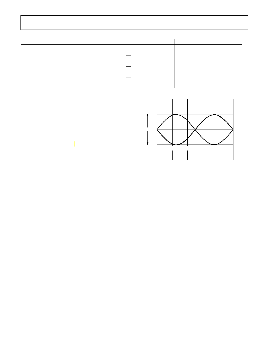
3.5V
VIN+
VIN
1.6V p-p
DIGITAL OUT = ALL 1s
DIGITAL OUT = ALL 0s
05490-054
Figure 57. Differential Analog Input Range for VREF = 1.6 V
The AD9446 analog input voltage range is offset from ground
by 3.5 V. Each analog input connects through a 1 k resistor to
the 3.5 V bias voltage and to the input of a differential buffer. The
internal bias network on the input properly biases the buffer for
maximum linearity and range (see the Equivalent Circuits
section). Therefore, the analog source driving the AD9446
should be ac-coupled to the input pins. The recommended
method for driving the analog input of the AD9446 is to use an
RF transformer to convert single-ended signals to differential
(see Figure 58). Series resistors between the output of the
transformer and the AD9446 analog inputs help isolate the
analog input source from switching transients caused by the
internal sample-and-hold circuit. The series resistors, along
with the 1 k resisters connected to the internal 3.5 V bias,
must be considered in impedance matching the transformer
input. For example, if R
T
is set to 51 , R
S
is set to 33 and
there is a 1:1 impedance ratio transformer, the input will match a
50 source with a full-scale drive of 16.0 dBm. The 50
impedance matching can also be incorporated on the secondary
side of the transformer, as shown in the evaluation board
schematic (see Figure 61).
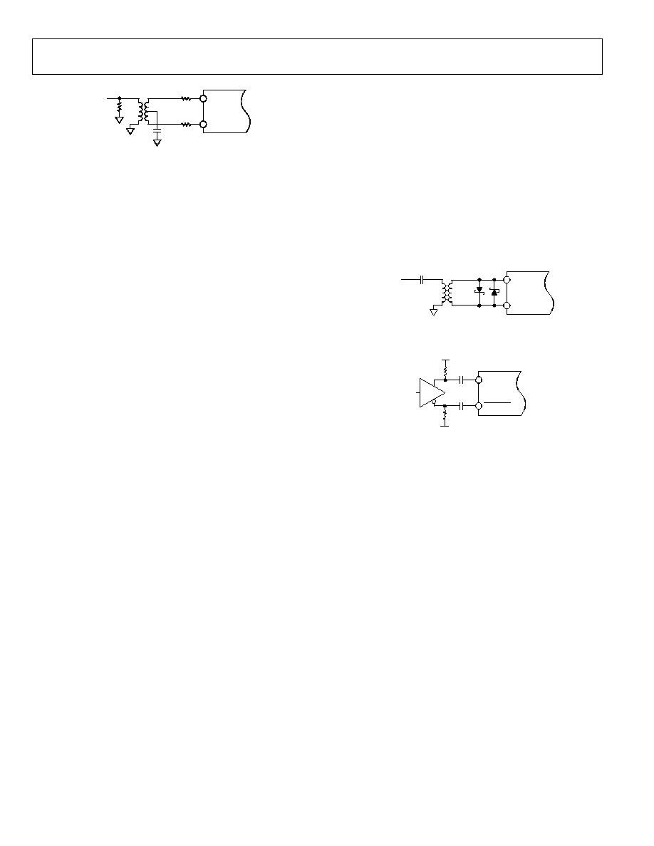
AD9446
Rev. 0 | Page 26 of 36
05490-055
0.1
F
R
T
AD9446
VIN+
VIN
R
S
R
S
ADT11WT
ANALOG
INPUT
SIGNAL
Figure 58. Transformer-Coupled Analog Input Circuit
CLOCK INPUT CONSIDERATIONS
Any high speed ADC is extremely sensitive to the quality of the
sampling clock provided by the user. A track-and-hold circuit is
essentially a mixer, and any noise, distortion, or timing jitter on
the clock is combined with the desired signal at the analog-to-
digital output. For that reason, considerable care was taken in
the design of the clock inputs of the AD9446, and the user is
advised to give careful thought to the clock source.
Typical high speed ADCs use both clock edges to generate a
variety of internal timing signals and, as a result, may be sensitive
to the clock duty cycle. Commonly a 5% tolerance is required on
the clock duty cycle to maintain dynamic performance charac-
teristics. The AD9446 contains a clock duty cycle stabilizer (DCS)
that retimes the nonsampling edge, providing an internal clock
signal with a nominal ~50% duty cycle. Noise and distortion per-
formance are nearly flat for a 30% to 70% duty cycle with the DCS
enabled. The DCS circuit locks to the rising edge of CLK+ and
optimizes timing internally. This allows for a wide range of input
duty cycles at the input without degrading performance. Jitter in
the rising edge of the input is still of paramount concern and is
not reduced by the internal stabilization circuit. The duty cycle
control loop does not function for clock rates of less than 30 MHz
nominally. The loop is associated with a time constant that
should be considered in applications where the clock rate can
change dynamically, requiring a wait time of 1.5 s to 5 s after a
dynamic clock frequency increase or decrease before the DCS
loop is relocked to the input signal. During the time that the
loop is not locked, the DCS loop is bypassed, and the internal
device timing is dependent on the duty cycle of the input clock
signal. In such an application, it may be appropriate to disable the
duty cycle stabilizer. In all other applications, enabling the DCS
circuit is recommended to maximize ac performance.
The DCS circuit is controlled by the DCS MODE pin; a CMOS
logic low (AGND) on DCS MODE enables the duty cycle stabilizer,
and logic high (AVDD1 = 3.3 V) disables the controller.
The AD9446 input sample clock signal must be a high quality,
extremely low phase noise source to prevent degradation of per-
formance. Maintaining 16-bit accuracy places a premium on the
encode clock phase noise. SNR performance can easily degrade
by 3 dB to 4 dB with 70 MHz analog input signals when using a
high jitter clock source. (See the
AN-501 Application Note
,
"Aperture Uncertainty and ADC System Performance.") For
optimum performance, the AD9446 must be clocked differentially.
The sample clock inputs are internally biased to ~1.5 V, and the
input signal is usually ac-coupled into the CLK+ and CLK- pins
via a transformer or capacitors. Figure 59 shows one preferred
method for clocking the AD9446. The clock source (low jitter)
is converted from single-ended to differential using an RF trans-
former. The back-to-back Schottky diodes across the secondary
of the transformer limit clock excursions into the AD9446 to
approximately 0.8 V p-p differential. This helps prevent the large
voltage swings of the clock from feeding through to other portions
of the AD9446 and limits the noise presented to the sample
clock inputs.
If a low jitter clock is available, it may help to band-pass filter
the clock reference before driving the ADC clock inputs. Another
option is to ac couple a differential ECL/PECL signal to the encode
input pins, as shown in Figure 60.
05490-056
0.1
F
AD9446
CLK+
CLK
HSMS2812
DIODES
CRYSTAL
SINE
SOURCE
ADT11WT
Figure 59. Crystal Clock Oscillator, Differential Encode
05490-057
0.1
F
AD9446
ENCODE
ENCODE
0.1
F
VT
VT
ECL/
PECL
Figure 60. Differential ECL for Encode
Jitter Considerations
High speed, high resolution ADCs are sensitive to the quality
of the clock input. The degradation in SNR at a given input
frequency (f
INPUT
) and rms amplitude due only to aperture jitter
(t
J
) can be calculated using the following equation:
SNR
= 20 log[2f
INPUT
× t
J
]
In the equation, the rms aperture jitter represents the root-mean-
square of all jitter sources, which includes the clock input, analog
input signal, and ADC aperture jitter specification. IF under-
sampling applications are particularly sensitive to jitter
The clock input should be treated as an analog signal in cases
where aperture jitter may affect the dynamic range of the AD9446.
Power supplies for clock drivers should be separated from the
ADC output driver supplies to avoid modulating the clock signal
with digital noise. Low jitter crystal-controlled oscillators make
the best clock sources. If the clock is generated from another type
of source (by gating, dividing, or another method), it should be
synchronized by the original clock during the last step.

AD9446
Rev. 0 | Page 27 of 36
POWER CONSIDERATIONS
Care should be taken when selecting a power source. The use of
linear dc supplies is highly recommended. Switching supplies
tend to have radiated components that may be received by the
AD9446. Each of the power supply pins should be decoupled as
closely to the package as possible using 0.1 F chip capacitors.
The AD9446 has separate digital and analog power supply pins.
The analog supplies are denoted AVDD1 (3.3 V) and AVDD2
(5 V), and the digital supply pins are denoted DRVDD. Although
the AVDD1 and DRVDD supplies can be tied together, best per-
formance is achieved when the supplies are separate. This is
because the fast digital output swings can couple switching
current back into the analog supplies. Note that both AVDD1
and AVDD2 must be held within 5% of the specified voltage.
The DRVDD supply of the AD9446 is a dedicated supply for the
digital outputs in either LVDS or CMOS output mode. When in
LVDS mode, the DRVDD should be set to 3.3 V. In CMOS mode,
the DRVDD supply can be connected from 2.5 V to 3.6 V for
compatibility with the receiving logic.
DIGITAL OUTPUTS
LVDS Mode
The off-chip drivers on the chip can be configured to provide
LVDS-compatible output levels via Pin 3 (OUTPUT MODE).
LVDS outputs are available when OUTPUT MODE is CMOS
logic high (or AVDD1 for convenience) and a 3.74 k R
SET
resistor is placed at Pin 5 (LVDS_BIAS) to ground. Dynamic
performance, including both SFDR and SNR, is maximized
when the AD9446 is used in LVDS mode; designers are
encouraged to take advantage of this mode. The AD9446
outputs include complimentary LVDS outputs for each data bit
(Dx+/Dx-), the overrange output (OR+/OR-), and the output
data clock output (DCO+/DCO-). The R
SET
resistor current is
multiplied on-chip, setting the output current at each output
equal to a nominal 3.5 mA (11 × I
RSET
). A 100 differential
termination resistor placed at the LVDS receiver inputs results
in a nominal 350 mV swing at the receiver. LVDS mode
facilitates interfacing with LVDS receivers in custom ASICs and
FPGAs that have LVDS capability for superior switching
performance in noisy environments. Single point-to-point net
topologies are recommended, with a 100 termination resistor
located as close to the receiver as possible. It is recommended to
keep the trace length less than 2 inches and to keep differential
output trace lengths as equal as possible.
CMOS Mode
In applications that can tolerate a slight degradation in dynamic
performance, the AD9446 output drivers can be configured to
interface with 2.5 V or 3.3 V logic families by matching
DRVDD to the digital supply of the interfaced logic. CMOS
outputs are available when OUTPUT MODE is CMOS logic
low (or AGND for convenience). In this mode, the output data
bits, Dx, are single-ended CMOS, as is the overrange output,
OR+. The output clock is provided as a differential CMOS
signal, DCO+/DCO-. Lower supply voltages are recommended
to avoid coupling switching transients back to the sensitive
analog sections of the ADC. The capacitive load to the CMOS
outputs should be minimized, and each output should be
connected to a single gate through a series resistor (220 ) to
minimize switching transients caused by the capacitive loading.
TIMING
The AD9446 provides latched data outputs with a pipeline delay
of 13 clock cycles. Data outputs are available one propagation
delay (t
PD
) after the rising edge of CLK+. Refer to Figure 2 and
Figure 3 for detailed timing diagrams.

AD9446
Rev. 0 | Page 28 of 36
OPERATIONAL MODE SELECTION
Data Format Select
The data format select (DFS) pin of the AD9446 determines
the coding format of the output data. This pin is 3.3 V CMOS
compatible, with logic high (or AVDD1, 3.3 V) selecting twos
complement and DFS logic low (AGND) selecting offset binary
format. Table 10 summarizes the output coding.
Output Mode Select
The OUPUT MODE pin controls the logic compatibility,
as well as the pinout of the digital outputs. This pin is a CMOS-
compatible input. With OUTPUT MODE = 0 (AGND), the
AD9446 outputs are CMOS compatible, and the pin assignment
for the device is as defined in Table 8. With OUTPUT MODE = 1
(AVDD1, 3.3 V), the AD9446 outputs are LVDS compatible, and
the pin assignment for the device is as defined in Table 7.
Duty Cycle Stabilizer
The DCS circuit is controlled by the DCS MODE pin; a CMOS
logic low (AGND) on DCS MODE enables the DCS, and logic
high (AVDD1, 3.3 V) disables the controller.
Table 10. Digital Output Coding
Code
VIN+ - VIN-
Input Span = 3.2 V p-p (V)
VIN+ - VIN-
Input Span = 2 V p-p (V)
Digital Output
Offset Binary (D15······D0)
Digital Output
Twos Complement (D15······D0)
65,536 +1.600
+1.000
1111 1111 1111 1111
0111 1111 1111 1111
32,768
0
0
1000 0000 0000 0000
0000 0000 0000 0000
32,767
-0.0000488
-0.000122
0111 1111 1111 1111
1111 1111 1111 1111
0
-1.60
-1.00
0000 0000 0000 0000
1000 0000 0000 0000

AD9446
Rev. 0 | Page 29 of 36
EVALUATION BOARD
Evaluation boards are offered to configure the AD9446 in either
CMOS or LVDS mode only. This design represents a recom-
mended configuration for using the device over a wide range of
sampling rates and analog input frequencies. These evaluation
boards provide all the support circuitry required to operate
the ADC in its various modes and configurations. Complete
schematics are shown in Figure 61 through Figure 64. Gerber
files are available from engineering applications demonstrating
the proper routing and grounding techniques that should be
applied at the system level.
It is critical that signal sources with very low phase noise
(<60 fsec rms jitter) be used to realize the ultimate performance
of the converter. Proper filtering of the input signal to remove
harmonics and lower the integrated noise at the input is also
necessary to achieve the specified noise performance.
The evaluation boards are shipped with a 115 V ac to 6 V dc
power supply. The evaluation boards include low dropout
regulators to generate the various dc supplies required by the
AD9446 and its support circuitry. Separate power supplies are
provided to isolate the DUT from the support circuitry. Each
input configuration can be selected by proper connection of
various jumpers (see Figure 61).
The LVDS mode evaluation boards include an LVDS-to-CMOS
translator, making them compatible with the high speed ADC
FIFO evaluation kit (HSC-ADC-EVALA-SC). The kit includes a
high speed data capture board that provides a hardware solution
for capturing up to 32 kB samples of high speed ADC output
data in a FIFO memory chip (user upgradeable to 256 kB
samples). Software is provided to enable the user to download
the captured data to a PC via the USB port. This software also
includes a behavioral model of the AD9446 and many other
high speed ADCs.
Behavioral modeling of the AD9446 is also available at
www.analog.com/ADIsimADC. The ADIsimADCTM software
supports virtual ADC evaluation using ADI proprietary behavioral
modeling technology. This allows rapid comparison between the
AD9446 and other high speed ADCs with or without hardware
evaluation boards.
The user can choose to remove the translator and terminations
to access the LVDS outputs directly.
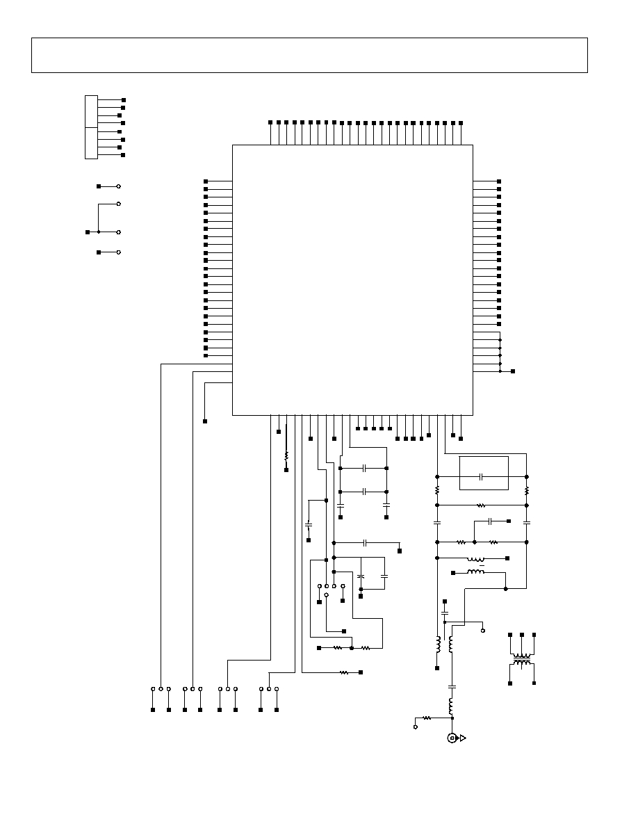
AD9446
Rev. 0 | Page 30 of 36
OPTIONAL
15
20
23
97
96
86
12
21
22
16
95
24
25
26
27
34
92
93
94
28
29
30
31
40
39
19
41
42
35
38
90
91
87
18
9
64
63
43
44
72
73
76
77
78
79
80
81
45
46
49
50
51
52
55
56
57
58
59
60
65
66
68
69
70
71
6
88
84
85
48
53
61
67
74
82
47
54
62
75
83
32
33
100
89
36
37
101
98
7
14
13
10
99
11
17
2
3
4
5
8
1
R11 1k
VCC
GND
R3
3.74k
DRGND
DRVDD
E24
EXTREF
D0_C (LSB)
D0_T
D1_C
D1_T
D3_C
D3_T
D4_C
D4_T
D5_C
D5_T
D7_C
D7_T
DR
D8_C/D0_Y
D8_T/D1_Y
D9_C/D2_Y
D9_T/D3_Y
D10_C/D4_Y
C98
DNP
GND
D15_C/D14_Y
E41
E25
E27
E26
VCC
GND
E6
E5
E4
GND
C3
0.1
F
C9
0.1
F
C86
0.1
F
R1
DNP
GND
5V
VCC
D14_C/D12_Y
DRGND
D6_T
D2_T
DRGND
D13_T/D11_Y
D10_T/D5_Y
DRB
D6_C
D2_C
DRVDD
D14_T/D13_Y
GND
VCC
D13_C/D10_Y
D12_T/D9_Y
D12_C/D8_Y
D11_T/D7_Y
D11_C/D6_Y
DRVDD
VCC
VCC
GND
VCC
VCC
VCC
5V
VCC
ENCB
GND
ENC
GND
VCC
5V
VCC
5V
GND
VCC
5V
5V
5V
5V
5V
GND
SCLK
VCC
VCC
GND
VCC
GND
5V
C13
DNP
R35
33
R28
33
R9
DNP
C91
0.1
F
C8
0.1
F
GND
GND
VCC
GND
VCC
EPAD
A
D
9445/
A
D
9446
U1
R4
36
P1
P2
P3
P22
PTMICRO4
VCC
5V
GND
GND
P4
1
2
3
4
P1
P2
P3
P21
PTMICRO4
EXTREF
DRVDD
XTALPWR
DRGND
P4
1
2
3
4
DCS MODE
DNC
OUTPUT MODE
DFS
LVDSBIAS
AVDD1
SENSE
VREF
AGND
REFT
REFB
AVDD2
AVDD2
AVDD2
AVDD2
AVDD2
AVDD2
AVDD1
AVDD1
AVDD1
AGND
VIN+
VIN
AGND
AVDD2
VCC
DRGND
DOR_C
DOR_T/DOR_Y
GND
VCC
VCC
DRVDD
(MSB) D15_T/D15_Y
E1
E9
E10
GND
VCC
E14
E2
E3
GND
VCC
E66
E18
E19
GND
VCC
C12
0.1
F
C5
0.1
F
J4
SMBMST
R5
DNP
GND
TINB
GND
ANALOG
L1
10nH
E15
R6
36
R2
DNP
C51
10
F
C2
0.1
F
C40
0.1
F
GND
GND
05490-
059
DRGND
D10_T
D10_C
D9_T
D9_C
D8_T
D8_C
DCO
DCOB
D7_T
D7_C
DRVDD
DRGND
D6_T
D6_C
D5_T
D5_C
D4_T
D4_C
D3_T
D3_C
D2_T
D2_C
D1_T
D1_C
D12_T
D12_C
D11_T
D11_C
DRVDD
AGND
AGND
AGND
AVDD1
AVDD1
AVDD1
AVDD1
OR_C
OR_T
AGND
AVDD1
AVDD1
DRVDD
DRGND
D15_T
D15_C
D14_T
D14_C
D13_T
D13_C
AVDD2
AVDD2
AVDD2
AVDD2
AVDD2
AVDD2
AVDD1
AVDD1
AVDD1
AVDD2
AVDD1
AVDD2
AVDD1
ENC
AGND
ENCB
AGND
AVDD1
AVDD1
AVDD1
AGND
DRGND
DRVDD
D0_C
D0_T
H4
MTHOLE6
GND
DRGND
H3
MTHOLE6
H1
MTHOLE6
H2
MTHOLE6
GND
C39
10
F
+
TOUT
CT
TOUTB
C7
0.1
F
PRI
SEC
GND
GND
T5
ADT1-1WT
T2
1 5
3
6
2
4
NC
GND
GND
TINB
TOUTB
TOUT
CT
PRI
SEC
ETC1-1-13
3
4
1
2
5
PRI
SEC
T1
ETC1-1-13
15
34
2
Figure 61. AD9446 Evaluation Board Schematic
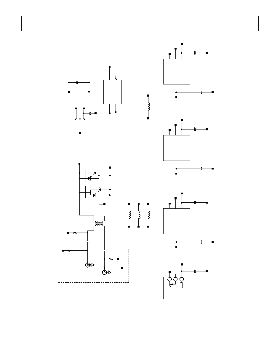
AD9446
Rev. 0 | Page 31 of 36
IN
OUT
OUT1
5V
C3
4
10
F
C8
9
10
F
3
4
2
1
ADP3338
U1
4
GND
GND
GND
5VX
5VX
5VX
5V
GND
VIN
GND
+
+
IN
OUT
OUT1
3.3V
L3
FERRITE
C6
10
F
C8
7
10
F
3
4
2
1
ADP3338
U7
GND
GND
V
CCX
V
CCX
GND
VIN
GND
+
+
IN
OUT
OUT1
3.3V
C4
10
F
C8
8
10
F
3
4
2
1
ADP3338
U3
DRGND
DRGND
DRV
DD
X
DRV
DDX
DRGND
VIN
GND
+
+
PJ-
102A
C3
3
10
F
1
3
2
P4
GND
VIN
+
1
3
2
POWER OPT
I
ONS
A
D
T
1-
1W
T
PR
I
SEC
NC
EN
C
E
NCB
GND
J5
SM
B
M
ST
R7
DNP
DNP
R3
9
0
R8
50
C2
6
0.1
F
C3
6
DNP
1
2
3
5
6
T3
2
3
1
CR2
CR1
C4
2
0.1
F
GND
XTA
L
IN
PU
T
GND
CR2
TO MAKE
LAY
O
UT AND P
ARAS
ITIC
LOADING S
Y
MME
TRICAL
4
J1
SM
B
M
ST
1
3
2
ENCODE
GND
OUT
VC
C
VEE
~
O
U
T
+
GND
GND
XTA
L
IN
PU
T
E30
C1
10
F
E31
8
14
7
U6
EC
LOSC
E20
VXTA
L
GND
5V
XTA
L
PW
R
VXTA
L
VXTA
L
1
+
C4
4
10
F
C4
1
0.1
F
OPTIONAL ENCODE CIRCUITS
V
CCX
VC
C
L4
FERRITE
DRV
DDX
DRV
DD
L5
FERRITE
DRGND
GND
L2
DNP
05490-060
Figure 62. AD9446 Evaluation Board Schematic (Continued)
AD9446
Rev. 0 | Page 32 of 36
C96
0.1
F
C97
0.1
F
C84
0.1
F
C46
0.1
F
C22
0.1
F
C59
0.1
F
C93
0.1
F
C94
0.1
F
C95
0.1
F
5V
GND
C60
0.1
F
C10
0.1
F
C61
0.1
F
C75
0.1
F
C27
0.1
F
C90
0.1
F
C50
0.1
F
C30
0.01
F
C28
0.1
F
C35
0.1
F
C32
0.1
F
VCC
BYPASS CAPACITORS
GND
C31
XX
C38
XX
C29
XX
C19
XX
C17
XX
C16
XX
C15
XX
C11
XX
C14
XX
VCC
GND
C37
0.1
F
C48
0.1
F
C18
0.1
F
C53
0.1
F
C52
0.1
F
C58
0.01
F
C56
10
F
+
C85
0.1
F
5V
GND
C110
XX
C108
XX
C109
XX
C72
XX
C73
XX
5V
GND
C21
0.1
F
C20
0.1
F
C65
10
F
+
C47
0.1
F
C23
0.1
F
DRVDD
DRGND
C64
10
F
+
C43
0.1
F
C45
XX
C49
XX
C69
XX
C70
XX
DRVDD
DRGND
C55
10
F
+
EXTREF
GND
05490-061
Figure 63. AD9446 Evaluation Board Schematic (Continued)
AD9446
Rev. 0 | Page 33 of 36
05490-062
R
SO16ISO
220
R8
R7
R6
R5
R4
R3
R1
R2
R
SO16ISO
220
8
7
6
5
4
3
1
2
16
15
14
13
12
11
10
9
RZ4
8
7
6
5
4
3
1
2
16
15
14
13
12
11
10
9
RZ5
D1
O
D0
O
D2
O
D4
O
D5
O
D6
O
D7
O
D3
O
D8
O
D9
O
D
10O
D
11O
D
12O
D
13O
D
14O
D
15O
GND5
V
CC6
V
CC5
GND4
EN
D
D4
Y
D3
Y
D2
Y
D1
Y
EN
C
C4
Y
C3
Y
C2
Y
C1
Y
GND3
V
CC4
V
CC3
GND2
B4
Y
B3
Y
B2
Y
B1
Y
EN
B
A4
Y
A3
Y
A2
Y
A1
Y
EN
A
GND1
V
CC2
V
CC1
GND
D4
B
D4
A
D3
B
D3
A
D2
B
D2
A
D1
B
D1
A
C4
B
C4
A
C3
B
C3
A
C2
B
C2
A
C1
B
C1
A
B4
B
B4
A
B3
B
B3
A
B2
B
B2
A
B1
B
B1
A
A4
B
A4
A
A3
B
A3
A
A2
B
A2
A
A1
B
A1
A
33
34
35
36
37
38
39
40
41
42
43
44
45
46
47
48
49
50
51
52
53
54
55
56
57
58
59
60
61
62
63
64
32
31
30
29
28
27
26
25
24
23
22
21
20
19
18
17
16
15
14
13
12
11
10
9
8
7
6
5
4
3
2
1
U8
SN
75LVD
S386
D
15_C
/D
14_Y
D
14_C
/D
12_Y
D
13_C
/D
10_Y
D
12_C
/D
8_Y
D
11_C
/D
6_Y
D
10_C
/D
4_Y
D
9_C
/D
2_Y
D
3_C
D
15_T/D
14_Y
D
14_T/D
13_Y
D
13_T/D
11_Y
D
12_T/D
9_Y
D
11_T/D
7_Y
D
10_T/D
5_Y
D
9_T/D
3_Y
D
8_T/D
1_Y
D
8_C
/D
0_Y
D
7_T
D
7_C
D
6_T
D
6_C
D
5_C
D
5_T
D
4_T
D
4_C
D
3_T
D
2_T
D
2_C
D
1_T
D
1_C
D
0_T
D
0_C
DRV
DD
DRV
DD
DRGND
DRGND
DRGND
DRV
DD
DRV
DD
DRGND
DRV
DD
DRV
DD
DRGND
DRV
DD
DRV
DD
DRV
DD
DRV
DD
DRGND
P1
P3
P5
P7
P9
P11
P13
P15
P17
P19
P21
P23
P25
P27
P29
P31
P33
P35
P37
P39
P2
P4
P6
P8
P10
P12
P14
P16
P18
P20
P22
P24
P26
P28
P30
P32
P34
P36
P38
P40
P6
C
40M
S
1
3
5
7
9
11
13
15
17
19
21
23
25
27
29
31
33
35
37
39
2
4
6
8
10
12
14
16
18
20
22
24
26
28
30
32
34
36
38
40
D
14_C
/D
12_Y
D
12_C
/D
8_Y
D
10_C
/D
4_Y
D8_C/DO_Y
DRB
D
7_C
D
4_C
D
3_C
D
2_C
D
5_C
D
6_C
D
9_C
/D
2_Y
D
11_C
/D
6_Y
D
13_C
/D
10_Y
D
1_C
DOR_
C
DRGND
D
15_C
/D
14_Y
DRGND
D
0_C
D
14_T/D
13_Y
D
12_T/D
9_Y
D
10_T/D
5_Y
D
8_T/D
1_Y
DR
D
7_T
D
4_T
D
3_T
D
2_T
D
5_T
D
6_T
D
9_T/D
3_Y
D
11_T/D
7_Y
D
13_T/D
11_Y
D
1_T
DOR_
T/DOR_
Y
DRGND
D
15_T/D
15_Y
DRGND
D
0_T
R8
R7
R6
R5
R4
R3
R1
R2
EN
_3_4
4Y
3Y
GND
VC
C
2Y
1Y
EN
_1_2
4B
4A
3B
3A
2B
2A
1B
1A
9
10
11
12
13
14
15
16
8
7
6
5
4
3
2
1
U1
5
SN
75LVD
T390
R1
9
0
R2
0
0
DRB
DOR_
C
DR
DRO_T/DOR_Y
DRO
DRV
DD
DRV
DD
DRGND
ORO
DRV
DD
C7
6
0.1
F
C8
2
0.1
F
C7
7
0.1
F
C7
8
0.1
F
GND
GND
P1
P3
P5
P7
P9
P11
P13
P15
P17
P19
P21
P23
P25
P27
P29
P31
P33
P35
P37
P39
P2
P4
P6
P8
P10
P12
P14
P16
P18
P20
P22
P24
P26
P28
P30
P32
P34
P36
P38
P40
P7
C
40M
S
1
3
5
7
9
11
13
15
17
19
21
23
25
27
29
31
33
35
37
39
2
4
6
8
10
12
14
16
18
20
22
24
26
28
30
32
34
36
38
40
D
15O
D
13O
D
11O
D9
O
D8
O
D7
O
D4
O
D3
O
D2
O
D5
O
D6
O
D
10O
D
12O
D
14O
D1
O
DRO
DRGND
DRGND
GND??
DRGND
ORO
DRGND
D0
O
Figure 64. AD9446 Evaluation Board Schematic (Continued)
AD9446
Rev. 0 | Page 34 of 36
Table 11. AD9446 Customer Evaluation Board Bill of Material
Item Qty.
Reference
Designator Description
Package
Value
Manufacturer
Mfg.
Part
No.
1 7 C4, C6, C33, C34, C87,
C88, C89
Capacitor
TAJD
10 F
Digi-Key Corporation
478-1699-2
2 44
C2, C3, C5, C7, C8,
C9, C10, C11, C12,
C15, C20, C21, C22,
C23, C26, C27, C28,
C32, C35, C38, C40,
C42, C43, C46, C47,
C48, C50, C52, C53,
C59, C60, C76, C77,
C78, C82, C84, C85,
C86, C90, C91, C94,
C95, C96, C97
Capacitor
402
0.1 F
Digi-Key Corporation
PCC2146CT-ND
3
2
C30, C58
Capacitor
201
0.01 F
Digi-Key Corporation
445-1796-1-ND
4
4
C39, C56, C64, C65
Capacitor
TAJD
10 F
Digi-Key Corporation
478-1699-2
5
1
C51
Capacitor
805
10 F
Digi-Key Corporation
490-1717-1-ND
6 1 CR1
Diode
SOT23M5
Digi-Key
Corporation
MA3X71600LCT-
ND
7 1 CR2
Diode
SOT23M5
Digi-Key
Corporation
MA3X71600LCT-
ND
8 20
E1, E2, E3, E4, E5, E6,
E9, E10, E14, E18, E19,
E20, E24, E25, E26, E27,
E30, E31, E36, E41
Header EHOLE
Mouser
Electronics
517-6111TG
9
2
J1, J4
SMA
SMA
Digi-Key Corporation
ARFX1231-ND
10
1
L1
Inductor
0603A
10 nH
Coilcraft, Inc.
0603CS-10NXGBU
11
3
L3, L4, L5
EMIFIL®
BLM31PG500SN1L
1206MIL
Mouser
Electronics 81-BLM31P500S
12 1 P4
PJ-002A
PJ-002A
Digi-Key
Corporation
CP-002A-ND
13 1 P7
Header
C40MS
Samtec,
Inc.
TSW-120-08-L-D-
RA
14
1
R3
Resistor
402
3.74 k
Digi-Key Corporation
P3.74KLCT-ND
15
1
R8
Resistor
402
50
Digi-Key Corporation
P49.9LCT-ND
16
4
R10, R19, R39, L2
Resistor
402
0
Digi-Key Corporation
P0.0JCT-ND
17
1
R11
BRES402
402
1 k
Digi-Key Corporation
P1.0KLCT-ND
18
2
R28, R35
Resistor
402
33
Digi-Key Corporation
P33JCT-ND
19
2
RZ4, RZ5
Resistor array
16PIN
22
Digi-Key Corporation
742C163220JCT-
ND
20 2 T3,
T5
Transformer
ADT1-1WT
Mini-Circuits
ADT1-1WT
21
1
U1
AD9445BSVZ-125
SV-100-3
Analog Devices, Inc.
AD9445BSVZ-100
22 1 U14
ADP3338-5
SOT-
223HS
Analog Devices, Inc.
ADP3338-5
23 2 U3,
U7
ADP3338-3.3
SOT-
223HS
Analog Devices, Inc.
ADP3338-33
24 1 U8
SN75LVDT386
TSSOP64
Arrow
Electronics,
Inc.
SN75LVDT386
25 1 U15
SN75LVDT390
SOIC16PW
Arrow
Electronics,
Inc.
SN75LVDT390
26
2
R4, R6
Resistor
402
36
Digi-Key Corporation
P36JCT-ND
27
2
C1, C44, C55
1
Capacitor
TAJD
10 F
Digi-Key Corporation
478-1699-2
28 23 C13, C14, C16, C17,
C18, C19, C29, C31,
C36, C37, C41, C45,
C49, C61, C69, C70,
C72, C73, C75, C93,
C108, C109, C110
1
CAP402 402
XX
29 1 C98
1
Capacitor
805
10 F
Digi-Key Corporation
490-1717-1-ND
AD9446
Rev. 0 | Page 35 of 36
Item Qty.
Reference
Designator Description
Package
Value
Manufacturer
Mfg.
Part
No.
30 E15
1
Header EHOLE
Mouser
Electronics
517-6111TG
31 J5
1
SMA SMA
Digi-Key
Corporation
ARFX1231-ND
32 P6
1
Header C40MS
Samtec,
Inc.
TSW-120-08-L-D-
RA
33 2 R1,
R2
1
BRES402 402
XX
34
3
R5, R7, R9
1
BRES402 402
XX
35 1 U2
1
ECLOSC DIP4(14)
36
4
H1, H2, H3, H4
1
MTHOLE6 MTHOLE6
37 2 T1,
T2
1
Balun transformer
SM-22
M/A-COM
ETC1-1-13
38 2 P21,
P22
1
Term strip
PTMICRO4
Newark Electronics
1
Parts not populated.
AD9446
Rev. 0 | Page 36 of 36
OUTLINE DIMENSIONS
COMPLIANT TO JEDEC STANDARDS MS-026-AED-HD
0.27
0.22
0.17
1
25
26
49
76
100
75
50
14.00 BSC SQ
16.00 BSC SQ
0.50 BSC
LEAD PITCH
0.75
0.60
0.45
1.20
MAX
1
25
26
50
76
100
75
51
1.05
1.00
0.95
0.20
0.09
0.08 MAX
COPLANARITY
VIEW A
ROTATED 90
°
CCW
SEATING
PLANE
0° MIN
7°
3.5°
0°
0.15
0.05
VIEW A
PIN 1
TOP VIEW
(PINS DOWN)
BOTTOM VIEW
(PINS UP)
9.50 SQ
EXPOSED
PAD
NOTES
1. CENTER FIGURES ARE TYPICAL UNLESS OTHERWISE NOTED.
2. THE PACKAGE HAS A CONDUCTIVE HEAT SLUG TO HELP DISSIPATE HEAT AND ENSURE RELIABLE OPERATION OF
THE DEVICE OVER THE FULL INDUSTRIAL TEMPERATURE RANGE. THE SLUG IS EXPOSED ON THE BOTTOM OF
THE PACKAGE AND ELECTRICALLY CONNECTED TO CHIP GROUND. IT IS RECOMMENDED THAT NO PCB SIGNAL
TRACES OR VIAS BE LOCATED UNDER THE PACKAGE THAT COULD COME IN CONTACT WITH THE CONDUCTIVE
SLUG. ATTACHING THE SLUG TO A GROUND PLANE WILL REDUCE THE JUNCTION TEMPERATURE OF THE
DEVICE WHICH MAY BE BENEFICIAL IN HIGH TEMPERATURE ENVIRONMENTS.
Figure 65. 100-Lead Thin Quad Flat Package, Exposed Pad [TQFP_EP]
(SV-100-3)
Dimensions shown in millimeters
ORDERING GUIDE
Model
Temperature Range
Package Description
Package Option
AD9446BSVZ-80
1
40°C to +85°C
100-Lead TQFP_EP
SV-100-3
AD9446BSVZ-100
1
40°C to +85°C
100-Lead TQFP_EP
SV-100-3
AD9446-100LVDS/PCB
AD9446-100 LVDS Mode Evaluation Board
AD9446-80LVDS/PCB
AD9446-80 LVDS Mode Evaluation Board
1
Z = Pb-free part.
© 2005 Analog Devices, Inc. All rights reserved. Trademarks and
registered trademarks are the property of their respective owners.
D05490010/05(0)
Document Outline
- þÿ
- þÿ
- þÿ
- FUNCTIONAL BLOCK DIAGRAM
- þÿ
- þÿ
- þÿ
- þÿ
- þÿ
- þÿ
- þÿ
- þÿ
- þÿ
- þÿ
- þÿ
- þÿ