 | –≠–ª–µ–∫—Ç—Ä–æ–Ω–Ω—ã–π –∫–æ–º–ø–æ–Ω–µ–Ω—Ç: AD9744-EB | –°–∫–∞—á–∞—Ç—å:  PDF PDF  ZIP ZIP |
Document Outline
- FEATURES
- APPLICATIONS
- GENERAL DESCRIPTION
- FUNCTIONAL BLOCK DIAGRAM
- PRODUCT HIGHLIGHTS
- SPECIFICATIONS
- DC SPECIFICATIONS
- DYNAMIC SPECIFICATIONS
- DIGITAL SPECIFICATIONS
- ABSOLUTE MAXIMUM RATINGS
- THERMAL CHARACTERISTICS
- ORDERING GUIDE
- PIN CONFIGURATION
- PIN FUNCTION DESCRIPTIONS
- DEFINITIONS OF SPECIFICATIONS
- Linearity Error (Also Called Integral Nonlinearity or INL)
- Differential Nonlinearity (or DNL)
- Monotonicity
- Offset Error
- Gain Error
- Output Compliance Range
- Temperature Drift
- Power Supply Rejection
- Settling Time
- Glitch Impulse
- Spurious-Free Dynamic Range
- Total Harmonic Distortion (THD)
- Multitone Power Ratio
- Typical Performance Characteristics
- FUNCTIONAL DESCRIPTION
- REFERENCE OPERATION
- REFERENCE CONTROL AMPLIFIER
- DAC TRANSFER FUNCTION
- ANALOG OUTPUTS
- DIGITAL INPUTS
- CLOCK INPUT
- SOIC/TSSOP Packages
- LFCSP Package
- DAC TIMING
- Input Clock and Data Timing Relationship
- Sleep Mode Operation
- POWER DISSIPATION
- APPLYING THE AD9744
- DIFFERENTIAL COUPLING USING A TRANSFORMER
- DIFFERENTIAL COUPLING USING AN OP AMP
- SINGLE-ENDED UNBUFFERED VOLTAGE OUTPUT
- SINGLE-ENDED, BUFFERED VOLTAGE OUTPUT CONFIGURATION
- POWER AND GROUNDING CONSIDERATIONS, POWER SUPPLY REJECTION
- EVALUATION BOARD
- OUTLINE DIMENSIONS
- Revision History
REV. A
Information furnished by Analog Devices is believed to be accurate and
reliable. However, no responsibility is assumed by Analog Devices for its
use, nor for any infringements of patents or other rights of third parties that
may result from its use. No license is granted by implication or otherwise
under any patent or patent rights of Analog Devices. Trademarks and
registered trademarks are the property of their respective companies.
One Technology Way, P.O. Box 9106, Norwood, MA 02062-9106, U.S.A.
Tel: 781/329-4700
www.analog.com
Fax: 781/326-8703
© 2003 Analog Devices, Inc. All rights reserved.
AD9744
*
14-Bit, 165 MSPS
TxDAC
Æ
D/A Converter
*Protected by U.S. Patent Numbers 5568145, 5689257, and 5703519.
FEATURES
High Performance Member of Pin Compatible
TxDAC Product Family
Excellent Spurious-Free Dynamic Range Performance
SFDR to Nyquist:
83 dBc @ 5 MHz Output
80 dBc @ 10 MHz Output
73 dBc @ 20 MHz Output
SNR @ 5 MHz Output, 125 MSPS: 77 dB
Twos Complement or Straight Binary Data Format
Differential Current Outputs: 2 mA to 20 mA
Power Dissipation: 135 mW @ 3.3 V
Power-Down Mode: 15 mW @ 3.3 V
On-Chip 1.2 V Reference
CMOS Compatible Digital Interface
28-Lead SOIC, 28-Lead TSSOP, and 32-Lead LFCSP
Packages
Edge-Triggered Latches
APPLICATIONS
Wideband Communication Transmit Channel:
Direct IF
Base Stations
Wireless Local Loop
Digital Radio Link
Direct Digital Synthesis (DDS)
Instrumentation
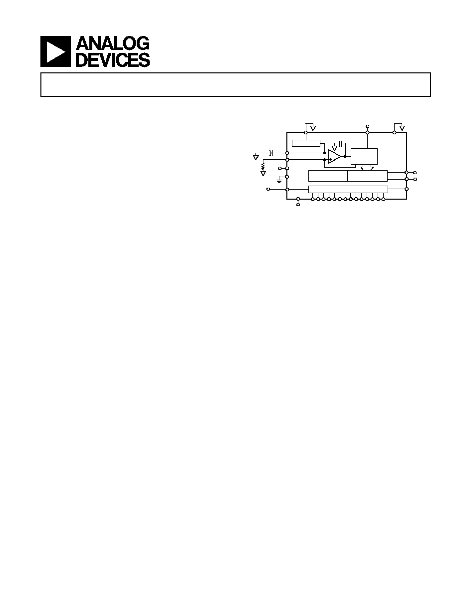
FUNCTIONAL BLOCK DIAGRAM
150pF
+1.2V REF
AVDD
ACOM
REFLO
CURRENT
SOURCE
ARRAY
3.3V
SEGMENTED
SWITCHES
LSB
SWITCHES
REFIO
FS ADJ
DVDD
DCOM
CLOCK
3.3V
R
SET
0.1 F
CLOCK
IOUTA
IOUTB
LATCHES
AD9744
SLEEP
DIGITAL DATA INPUTS (DB13≠DB0)
MODE
GENERAL DESCRIPTION
The AD9744 is a 14-bit resolution, wideband, third generation
member of the TxDAC series of high performance, low power
CMOS digital-to-analog converters (DACs). The TxDAC family,
consisting of pin compatible 8-, 10-, 12-, and 14-bit DACs, is
specifically optimized for the transmit signal path of communi-
cation systems. All of the devices share the same interface options,
small outline package, and pinout, providing an upward or down-
ward component selection path based on performance, resolution,
and cost. The AD9744 offers exceptional ac and dc performance
while supporting update rates up to 165 MSPS.
The AD9744's low power dissipation makes it well suited for
portable and low power applications. Its power dissipation can
be further reduced to a mere 60 mW with a slight degradation
in performance by lowering the full-scale current output. Also,
a power-down mode reduces the standby power dissipation to
approximately 15 mW. A segmented current source architec-
ture is combined with a proprietary switching technique to
reduce spurious components and enhance dynamic performance.
Edge-triggered input latches and a 1.2 V temperature compen-
sated band gap reference have been integrated to provide a
complete monolithic DAC solution. The digital inputs support
3 V CMOS logic families.
PRODUCT HIGHLIGHTS
1. The AD9744 is the 14-bit member of the pin compatible
TxDAC family, which offers excellent INL and DNL
performance.
2. Data input supports twos complement or straight binary
data coding.
3. High speed, single-ended CMOS clock input supports
165 MSPS conversion rate.
4. Low power: Complete CMOS DAC function operates on
135 mW from a 2.7 V to 3.6 V single supply. The DAC
full-scale current can be reduced for lower power operation,
and a sleep mode is provided for low power idle periods.
5. On-chip voltage reference: The AD9744 includes a 1.2 V
temperature compensated band gap voltage reference.
6. Industry-standard 28-lead SOIC, 28-lead TSSOP, and 32-lead
LFCSP packages.

REV. A
≠2≠
AD9744≠SPECIFICATIONS
(T
MIN
to T
MAX
, AVDD = 3.3 V, DVDD = 3.3 V, CLKVDD = 3.3 V, I
OUTFS
= 20 mA, unless otherwise noted.)
DC SPECIFICATIONS
Parameter
Min
Typ
Max
Unit
RESOLUTION
14
Bits
DC ACCURACY
1
Integral Linearity Error (INL)
≠5
±0.8
+5
LSB
Differential Nonlinearity (DNL)
≠3
±0.5
+3
LSB
ANALOG OUTPUT
Offset Error
≠0.02
+0.02
% of FSR
Gain Error (Without Internal Reference)
≠0.5
±0.1
+0.5
% of FSR
Gain Error (With Internal Reference)
≠0.5
±0.1
+0.5
% of FSR
Full-Scale Output Current
2
2
20
mA
Output Compliance Range
≠1
+1.25
V
Output Resistance
100
k
W
Output Capacitance
5
pF
REFERENCE OUTPUT
Reference Voltage
1.14
1.20
1.26
V
Reference Output Current
3
100
nA
REFERENCE INPUT
Input Compliance Range
0.1
1.25
V
Reference Input Resistance (Ext. Reference)
1
M
W
Small Signal Bandwidth
0.5
MHz
TEMPERATURE COEFFICIENTS
Offset Drift
0
ppm of FSR/
C
Gain Drift (Without Internal Reference)
±50
ppm of FSR/
C
Gain Drift (With Internal Reference)
±100
ppm of FSR/
C
Reference Voltage Drift
±50
ppm/
C
POWER SUPPLY
Supply Voltages
AVDD
2.7
3.3
3.6
V
DVDD
2.7
3.3
3.6
V
CLKVDD
2.7
3.3
3.6
V
Analog Supply Current (I
AVDD
)
33
36
mA
Digital Supply Current (I
DVDD
)
4
8
9
mA
Clock Supply Current (I
CLKVDD
)
5
6
mA
Supply Current Sleep Mode (I
AVDD
)
5
6
mA
Power Dissipation
4
135
145
mW
Power Dissipation
5
145
mW
Power Supply Rejection Ratio--AVDD
6
≠1
+1
% of FSR/V
Power Supply Rejection Ratio--DVDD
6
≠0.04
+0.04
% of FSR/V
OPERATING RANGE
≠40
+85
C
NOTES
1
Measured at IOUTA, driving a virtual ground.
2
Nominal full-scale current, I
OUTFS
, is 32 times the I
REF
current.
3
An external buffer amplifier with input bias current <100 nA should be used to drive any external load.
4
Measured at f
CLOCK
= 25 MSPS and f
OUT
= 1 MHz.
5
Measured as unbuffered voltage output with I
OUTFS
= 20 mA and 50
W R
LOAD
at IOUTA and IOUTB, f
CLOCK
= 100 MSPS and f
OUT
= 40 MHz.
6
±5% power supply variation.
Specifications subject to change without notice.
REV. A
AD9744
≠3≠
DYNAMIC SPECIFICATIONS
Parameter
Min
Typ
Max
Unit
DYNAMIC PERFORMANCE
Maximum Output Update Rate (f
CLOCK
)
165
MSPS
Output Settling Time (t
ST
) (to 0.1%)
1
11
ns
Output Propagation Delay (t
PD
)
1
ns
Glitch Impulse
5
pV-s
Output Rise Time (10% to 90%)
1
2.5
ns
Output Fall Time (10% to 90%)
1
2.5
ns
Output Noise (I
OUTFS
= 20 mA)
2
50
pA/
˜Hz
Output Noise (I
OUTFS
= 2 mA)
2
30
pA/
˜Hz
Noise Spectral Density
3
≠155
dBm/Hz
AC LINEARITY
Spurious-Free Dynamic Range to Nyquist
f
CLOCK
= 25 MSPS; f
OUT
= 1.00 MHz
0 dBFS Output
77
90
dBc
≠6 dBFS Output
87
dBc
≠12 dBFS Output
82
dBc
≠18 dBFS Output
82
dBc
f
CLOCK
= 65 MSPS; f
OUT
= 1.00 MHz
85
dBc
f
CLOCK
= 65 MSPS; f
OUT
= 2.51 MHz
84
dBc
f
CLOCK
= 65 MSPS; f
OUT
= 10 MHz
80
dBc
f
CLOCK
= 65 MSPS; f
OUT
= 15 MHz
75
dBc
f
CLOCK
= 65 MSPS; f
OUT
= 25 MHz
74
dBc
f
CLOCK
= 165 MSPS; f
OUT
= 21 MHz
73
dBc
f
CLOCK
= 165 MSPS; f
OUT
= 41 MHz
60
dBc
Spurious-Free Dynamic Range within a Window
f
CLOCK
= 25 MSPS; f
OUT
= 1.00 MHz; 2 MHz Span
84
90
dBc
f
CLOCK
= 50 MSPS; f
OUT
= 5.02 MHz; 2 MHz Span
90
dBc
f
CLOCK
= 65 MSPS; f
OUT
= 5.03 MHz; 2.5 MHz Span
87
dBc
f
CLOCK
= 125 MSPS; f
OUT
= 5.04 MHz; 4 MHz Span
87
dBc
Total Harmonic Distortion
f
CLOCK
= 25 MSPS; f
OUT
= 1.00 MHz
≠86
≠77
dBc
f
CLOCK
= 50 MSPS; f
OUT
= 2.00 MHz
≠77
dBc
f
CLOCK
= 65 MSPS; f
OUT
= 2.00 MHz
≠77
dBc
f
CLOCK
= 125 MSPS; f
OUT
= 2.00 MHz
≠77
dBc
Signal-to-Noise Ratio
f
CLOCK
= 65 MSPS; f
OUT
= 5 MHz; I
OUTFS
= 20 mA
82
dB
f
CLOCK
= 65 MSPS; f
OUT
= 5 MHz; I
OUTFS
= 5 mA
88
dB
f
CLOCK
= 125 MSPS; f
OUT
= 5 MHz; I
OUTFS
= 20 mA
77
dB
f
CLOCK
= 125 MSPS; f
OUT
= 5 MHz; I
OUTFS
= 5 mA
78
dB
f
CLOCK
= 165 MSPS; f
OUT
= 5 MHz; I
OUTFS
= 20 mA
70
dB
f
CLOCK
= 165 MSPS; f
OUT
= 5 MHz; I
OUTFS
= 5 mA
70
dB
Multitone Power Ratio (8 Tones at 400 kHz Spacing)
f
CLOCK
= 78 MSPS; f
OUT
= 15.0 MHz to 18.2 MHz
0 dBFS Output
66
dBc
≠6 dBFS Output
68
dBc
≠12 dBFS Output
62
dBc
≠18 dBFS Output
61
dBc
NOTES
1
Measured single-ended into 50
W load.
2
Output noise is measured with a full-scale output set to 20 mA with no conversion activity. It is a measure of the thermal noise only.
3
Noise spectral density is the average noise power normalized to a 1 Hz bandwidth, with the DAC converting and producing an output tone.
Specifications subject to change without notice.
(T
MIN
to T
MAX
, AVDD = 3.3 V, DVDD = 3.3 V, CLKVDD = 3.3 V, I
OUTFS
= 20 mA, differential
transformer coupled output, 50 doubly terminated, unless otherwise noted.)
REV. A
≠4≠
AD9744
(T
MIN
to T
MAX
, AVDD = 3.3 V, DVDD = 3.3 V, CLKVDD = 3.3 V, I
OUTFS
= 20 mA, unless otherwise noted.)
DIGITAL SPECIFICATIONS
Parameter
Min
Typ
Max
Unit
DIGITAL INPUTS
1
Logic 1 Voltage
2.1
3
V
Logic 0 Voltage
0
0.9
V
Logic 1 Current
≠10
+10
mA
Logic 0 Current
≠10
+10
mA
Input Capacitance
5
pF
Input Setup Time (t
S
)
2.0
ns
Input Hold Time (t
H
)
1.5
ns
Latch Pulsewidth (t
LPW
)
1.5
ns
CLK INPUTS
2
Input Voltage Range
0
3
V
Common-Mode Voltage
0.75
1.5
2.25
V
Differential Voltage
0.5
1.5
V
NOTES
1
Includes CLOCK pin on SOIC/TSSOP packages and CLK+ pin on LFCSP package in single-ended clock input mode.
2
Applicable to CLK+ and CLK≠ inputs when configured for differential or PECL clock input mode.
Specifications subject to change without notice.
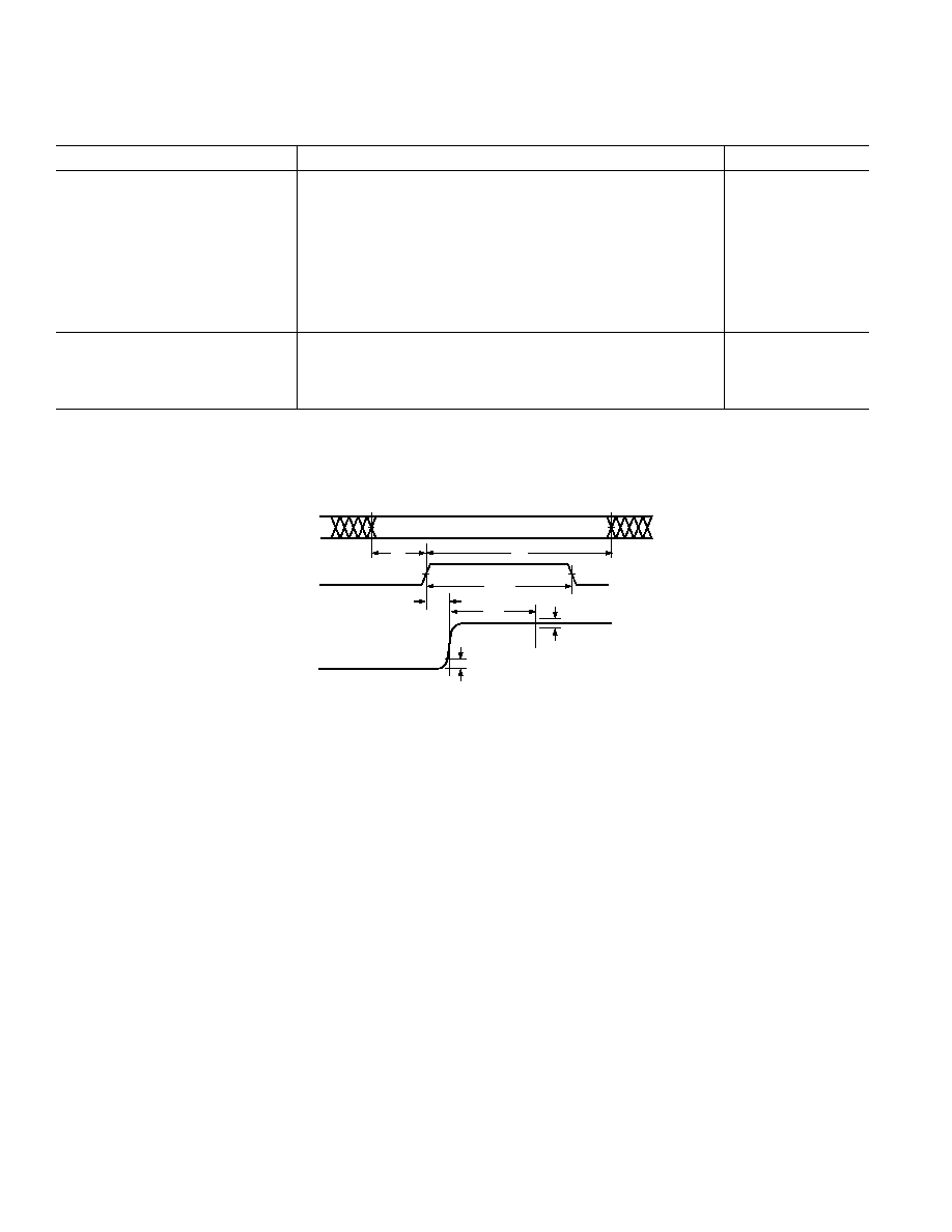
0.1%
0.1%
t
S
t
H
t
PD
t
ST
DB0≠DB13
CLOCK
IOUTA
OR
IOUTB
t
LPW
Figure 1. Timing Diagram
REV. A
AD9744
≠5≠
CAUTION
ESD (electrostatic discharge) sensitive device. Electrostatic charges as high as 4000 V readily
accumulate on the human body and test equipment and can discharge without detection. Although the
AD9744 features proprietary ESD protection circuitry, permanent damage may occur on devices
subjected to high energy electrostatic discharges. Therefore, proper ESD precautions are recommended
to avoid performance degradation or loss of functionality.
ABSOLUTE MAXIMUM RATINGS
*
With
Parameter
Respect to Min
Max
Unit
AVDD
ACOM
≠0.3
+3.9
V
DVDD
DCOM
≠0.3
+3.9
V
CLKVDD
CLKCOM ≠0.3
+3.9
V
ACOM
DCOM
≠0.3
+0.3
V
ACOM
CLKCOM ≠0.3
+0.3
V
DCOM
CLKCOM ≠0.3
+0.3
V
AVDD
DVDD
≠3.9
+3.9
V
AVDD
CLKVDD
≠3.9
+3.9
V
DVDD
CLKVDD
≠3.9
+3.9
V
CLOCK, SLEEP
DCOM
≠0.3
DVDD + 0.3
V
Digital Inputs, MODE
DCOM
≠0.3
DVDD + 0.3
V
IOUTA, IOUTB
ACOM
≠1.0
AVDD + 0.3
V
REFIO, REFLO, FS ADJ
ACOM
≠0.3
AVDD + 0.3
V
CLK+, CLK≠, CMODE
CLKCOM ≠0.3
CLKVDD + 0.3 V
Junction Temperature
150
C
Storage Temperature
≠65
+150
C
Lead Temperature (10 sec)
300
C
*Stresses above those listed under Absolute Maximum Ratings may cause perma-
nent damage to the device. This is a stress rating only; functional operation of the
device at these or any other conditions above those indicated in the operational
sections of this specification is not implied. Exposure to absolute maximum ratings
for extended periods may effect device reliability.
THERMAL CHARACTERISTICS
*
Thermal Resistance
28-Lead 300-Mil SOIC
JA
= 55.9
C/W
28-Lead TSSOP
JA
= 67.7
C/W
32-Lead LFCSP
JA
= 32.5
C/W
*Thermal impedance measurements were taken on a 4-layer board in still air,
in accordance with EIA/JESD51-7.
ORDERING GUIDE
Model
Temperature Range
Package Description
Package Options
*
AD9744AR
≠40
C to +85C
28-Lead 300-Mil SOIC
R-28
AD9744ARRL
≠40
C to +85C
28-Lead 300-Mil SOIC
R-28
AD9744ARU
≠40
C to +85C
28-Lead TSSOP
RU-28
AD9744ARURL7
≠40
C to +85C
28-Lead TSSOP
RU-28
AD9744ACP
≠40
C to +85C
32-Lead LFCSP
CP-32
AD9744ACPRL7
≠40
C to +85C
32-Lead LFCSP
CP-32
AD9744-EB
Evaluation Board (SOIC)
AD9744ACP-PCB
Evaluation Board (LFCSP)
*R = Small Outline IC; RU = Thin Shrink Small Outline Package; CP = Lead Frame Chip Scale Package
REV. A
≠6≠
AD9744
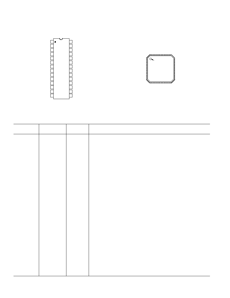
PIN CONFIGURATION
28-Lead SOIC and TSSOP
14
13
12
11
17
16
15
20
19
18
10
9
8
1
2
3
4
7
6
5
TOP VIEW
(Not to Scale)
28
27
26
25
24
23
22
21
AD9744
NC = NO CONNECT
DB9
DB8
DB7
DB6
DB5
DB4
DB3
DB2
DB1
(LSB) DB0
CLOCK
DVDD
DCOM
MODE
AVDD
RESERVED
IOUTA
IOUTB
ACOM
NC
FS ADJ
REFIO
REFLO
SLEEP
DB10
DB11
DB12
(MSB) DB13
PIN FUNCTION DESCRIPTIONS
SOIC/TSSOP
LFCSP
Pin No.
Pin No.
Mnemonic
Description
1
27
DB13
Most Significant Data Bit (MSB).
2≠13
28≠32, 1, 2, 4≠8
DB12≠DB1
Data Bits 12≠1.
14
9
DB0
Least Significant Data Bit (LSB).
15
25
SLEEP
Power-Down Control Input. Active high. Contains active pull-down circuit;
it may be left unterminated if not used.
16
N/A
REFLO
Reference Ground when Internal 1.2 V Reference Used. Connect to AVDD to
disable internal reference.
17
23
REFIO
Reference Input/Output. Serves as reference input when internal reference disabled
(i.e., tie REFLO to AVDD). Serves as 1.2 V reference output when internal
reference activated (i.e., tie REFLO to ACOM). Requires 0.1
mF capacitor to
ACOM when internal reference activated.
18
24
FS ADJ
Full-Scale Current Output Adjust.
19
N/A
NC
No Internal Connection.
20
19, 22
ACOM
Analog Common.
21
20
IOUTB
Complementary DAC Current Output. Full-scale current when all data bits are 0s.
22
21
IOUTA
DAC Current Output. Full-scale current when all data bits are 1s.
23
N/A
RESERVED Reserved. Do Not Connect to Common or Supply.
24
17, 18
AVDD
Analog Supply Voltage (3.3 V).
25
16
MODE
Selects Input Data Format. Connect to DCOM for straight binary, DVDD for
twos complement.
N/A
15
CMODE
Clock Mode Selection. Connect to CLKCOM for single-ended clock receiver
(drive CLK+ and float CLK≠). Connect to CLKVDD for differential receiver.
Float for PECL receiver (terminations on-chip).
26
10, 26
DCOM
Digital Common.
27
3
DVDD
Digital Supply Voltage (3.3 V).
28
N/A
CLOCK
Clock Input. Data latched on positive edge of clock.
N/A
12
CLK+
Differential Clock Input.
N/A
13
CLK≠
Differential Clock Input.
N/A
11
CLKVDD
Clock Supply Voltage (3.3 V).
N/A
14
CLKCOM
Clock Common.
32-Lead LFCSP
PIN 1
INDICATOR
TOP VIEW
24 FS ADJ
23 REFIO
22 ACOM
21 IOUTA
DB7 1
DB6 2
DVDD 3
32 DB8
20 IOUTB
19 ACOM
18 AVDD
17 AVDD
(
LSB) DB0 9
DCOM 10
CLKVDD 11
CLK
12
CLK
13
CLKCOM 14
CMODE 15
MODE 16
DB5 4
DB4 5
DB3 6
DB2 7
DB1 8
31 DB9
30 DB10
29 DB11
27 DB13 (MSB)
26 DCOM
25 SLEEP
AD9744
28 DB12
NC = NO CONNECT
REV. A
AD9744
≠7≠
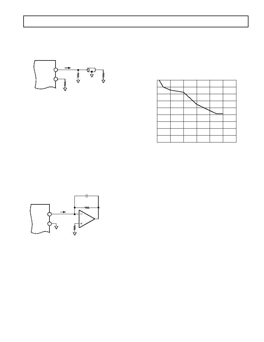
DEFINITIONS OF SPECIFICATIONS
Linearity Error (Also Called Integral Nonlinearity or INL)
Linearity error is defined as the maximum deviation of the
actual analog output from the ideal output, determined by a
straight line drawn from zero to full scale.
Differential Nonlinearity (or DNL)
DNL is the measure of the variation in analog value, normalized
to full scale, associated with a 1 LSB change in digital input code.
Monotonicity
A D/A converter is monotonic if the output either increases or
remains constant as the digital input increases.
Offset Error
The deviation of the output current from the ideal of zero is
called the offset error. For IOUTA, 0 mA output is expected
when the inputs are all 0s. For IOUTB, 0 mA output is expected
when all inputs are set to 1s.
Gain Error
The difference between the actual and ideal output span. The
actual span is determined by the output when all inputs are set
to 1s minus the output when all inputs are set to 0s.
Output Compliance Range
The range of allowable voltage at the output of a current output
DAC. Operation beyond the maximum compliance limits may
cause either output stage saturation or breakdown, resulting in
nonlinear performance.
Temperature Drift
Temperature drift is specified as the maximum change from the
ambient (25
C) value to the value at either T
MIN
or T
MAX
. For
offset and gain drift, the drift is reported in ppm of full-scale
range (FSR) per
C. For reference drift, the drift is reported in
ppm per
C.
Power Supply Rejection
The maximum change in the full-scale output as the supplies
are varied from nominal to minimum and maximum specified
voltages.
Settling Time
The time required for the output to reach and remain within a
specified error band about its final value, measured from the
start of the output transition.
Glitch Impulse
Asymmetrical switching times in a DAC give rise to undesired
output transients that are quantified by a glitch impulse. It is
specified as the net area of the glitch in pV-s.
Spurious-Free Dynamic Range
The difference, in dB, between the rms amplitude of the output
signal and the peak spurious signal over the specified bandwidth.
Total Harmonic Distortion (THD)
THD is the ratio of the rms sum of the first six harmonic compo-
nents to the rms value of the measured input signal. It is expressed
as a percentage or in decibels (dB).
Multitone Power Ratio
The spurious-free dynamic range containing multiple carrier
tones of equal amplitude. It is measured as the difference between
the rms amplitude of a carrier tone to the peak spurious signal
in the region of a removed tone.
150pF
+1.2V REF
AVDD
ACOM
REFLO
PMOS
CURRENT SOURCE
ARRAY
SEGMENTED SWITCHES
FOR DB13≠DB5
LSB
SWITCHES
REFIO
FS ADJ
DVDD
DCOM
CLOCK
3.3V
R
SET
2k
0.1 F
DVDD
DCOM
IOUTA
IOUTB
AD9744
SLEEP
50
RETIMED
CLOCK
OUTPUT*
LATCHES
DIGITAL
DATA
TEKTRONIX AWG-2021
WITH OPTION 4
LECROY 9210
PULSE GENERATOR
CLOCK
OUTPUT
50
50
RHODE & SCHWARZ
FSEA30
SPECTRUM
ANALYZER
MINI-CIRCUITS
T1-1T
*AWG2021 CLOCK RETIMED
SO THAT THE DIGITAL DATA
TRANSITIONS ON FALLING EDGE
OF 50% DUTY CYCLE CLOCK.
3.3V
MODE
Figure 2. Basic AC Characterization Test Set-Up (SOIC/TSSOP Packages)
REV. A
≠8≠
AD9744≠Typical Performance Characteristics
95
80
85
90
70
75
1
10
f
OUT
(MHz)
SFDR (dBc)
100
55
60
65
45
50
65MSPS
125MSPS
165MSPS
125MSPS (LFCSP)
165MSPS (LFCSP)
TPC 1. SFDR vs. f
OUT
@ 0 dBFS
90
75
80
85
65
70
0
10
20
30
f
OUT
(MHz)
SFDR (dBc)
40
50
60
55
65
60
50
45
0dBFS (LFCSP)
≠6dBFS (LFCSP)
≠12dBFS (LFCSP)
≠6dBFS
0dBFS
≠12dBFS
TPC 4. SFDR vs. f
OUT
@ 165 MSPS
95
90
85
80
75
70
65
60
≠25
≠20
≠15
≠10
A
OUT
(dBFS)
SFDR (dBc)
≠5
0
55
50
45
65MSPS
125MSPS
125MSPS (LFCSP)
165MSPS
165MSPS (LFCSP)
TPC 7. Single-Tone SFDR vs. A
OUT
@ f
OUT
= f
CLOCK
/5
0
5
25
10
15
20
45
50
55
60
65
70
75
80
85
90
95
0dBFS
≠6dBFS
f
OUT
(MHz)
SFDR (dBc)
≠12dBFS
TPC 2. SFDR vs. f
OUT
@ 65 MSPS
0
5
25
10
15
20
45
50
55
60
65
70
75
80
85
90
95
f
OUT
(MHz)
SFDR (dBc)
20mA
10mA
5mA
TPC 5. SFDR vs. f
OUT
and I
OUTFS
@ 65 MSPS and 0 dBFS
80
70
75
65
25
45
65
85
f
CLOCK
(MSPS)
SNR (dB)
105
125
145
165
60
55
50
20mA SOIC
20mA LFCSP
10mA SOIC
10mA LFCSP
5mA SOIC
5mA LFCSP
TPC 8. SNR vs. f
CLOCK
and I
OUTFS
@ f
OUT
= 5 MHz and 0 dBFS
0
5
45
10
15
35
45
50
55
60
65
70
75
80
85
90
95
0dBFS
≠6dBFS
≠12dBFS
f
OUT
(MHz)
SFDR (dBc)
40
30
20
25
TPC 3. SFDR vs. f
OUT
@ 125 MSPS
45
50
55
60
65
70
75
80
85
90
95
SFDR (dBc)
0
≠5
≠25
≠10
≠15
≠20
A
OUT
(dBFS)
65MSPS
125MSPS
165MSPS
TPC 6. Single-Tone SFDR vs. A
OUT
@ f
OUT
= f
CLOCK
/11
0
≠5
≠25
≠10
≠15
≠20
45
50
55
60
65
70
75
80
85
90
95
A
OUT
(dBFS)
SFDR (dBc)
65MSPS (8.3,10.3)
78MSPS (10.1, 12.1)
125MSPS (16.9, 18.9)
165MSPS (22.6, 24.6)
TPC 9. Dual-Tone IMD vs. A
OUT
@ f
OUT
= f
CLOCK
/7
REV. A
AD9744
≠9≠
4096
8192
12288
16384
≠1.0
≠0.5
0
0.5
1.0
CODE
ERR
OR (LSB)
0
≠1.5
1.5
TPC 10. Typical INL
1
6
26
11
16
21
≠100
FREQUENCY (MHz)
MA
GNITUDE (dBm)
31
f
CLOCK
= 78MSPS
f
OUT
= 15.0MHz
SFDR = 79dBc
AMPLITUDE = 0dBFS
36
≠90
≠80
≠70
≠60
≠50
≠40
≠20
0
≠10
≠30
TPC 13. Single-Tone SFDR
CENTER 33.22MHz
≠120
≠110
≠100
≠90
≠80
≠70
≠60
≠40
≠20
≠30
≠50
3MHz
SPAN 30MHz
CU1
C0
C0
C11
C11
C12
C12
CU1
CU2
CU2
≠39.01dBm
29.38000000MHz
CH PWR ≠19.26dBm
ACP UP ≠64.98dB
ACP LOW +0.55dB
ALT1 UP ≠66.26dB
ALT1 LOW ≠64.23dB
MA
GNITUDE (dBm)
TPC 16. Two-Carrier UMTS
Spectrum (ACLR = 64 dB)
0
4096
1.0
0.8
≠0.6
0.4
0.2
0
CODE
ERR
OR (LSB)
≠0.2
≠1.0
≠0.8
≠0.4
0.6
8192
12288
16384
TPC 11. Typical DNL
1
6
26
11
16
21
≠100
FREQUENCY (MHz)
MA
GNITUDE (dBm)
31
f
CLOCK
= 78MSPS
f
OUT1
= 15.0MHz
f
OUT2
= 15.4MHz
SFDR = 77dBc
AMPLITUDE = 0dBFS
36
≠90
≠80
≠70
≠60
≠50
≠40
≠20
0
≠10
≠30
TPC 14. Dual-Tone SFDR
≠40
≠20
60
0
20
40
50
55
60
65
70
75
80
85
90
4MHz
19MHz
34MHz
TEMPERATURE ( C)
SFDR (dBc)
80
49MHz
95
45
TPC 12. SFDR vs. Temperature
@ 165 MSPS, 0 dBFS
1
6
26
11
16
21
≠100
FREQUENCY (MHz)
MA
GNITUDE (dBm)
31
f
CLOCK
= 78MSPS
f
OUT1
= 15.0MHz
f
OUT2
= 15.4MHz
f
OUT3
= 15.8MHz
f
OUT4
= 16.2MHz
SFDR = 75dBc
AMPLITUDE = 0dBFS
36
≠90
≠80
≠70
≠60
≠50
≠40
≠20
0
≠10
≠30
TPC 15. Four-Tone SFDR
REV. A
≠10≠
AD9744
FUNCTIONAL DESCRIPTION
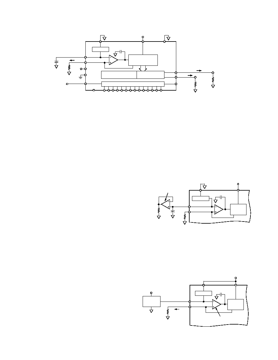
Figure 3 shows a simplified block diagram of the AD9744. The
AD9744 consists of a DAC, digital control logic, and full-scale
output current control. The DAC contains a PMOS current
source array capable of providing up to 20 mA of full-scale
current (I
OUTFS
). The array is divided into 31 equal currents
that make up the five most significant bits (MSBs). The next
four bits, or middle bits, consist of 15 equal current sources
whose value is 1/16th of an MSB current source. The remaining
LSBs are binary weighted fractions of the middle bits current
sources. Implementing the middle and lower bits with current
sources, instead of an R-2R ladder, enhances its dynamic per-
formance for multitone or low amplitude signals and helps
maintain the DAC's high output impedance (i.e., >100 k
W).
All of these current sources are switched to one or the other of
the two output nodes (i.e., IOUTA or IOUTB) via PMOS
differential current switches. The switches are based on the
architecture that was pioneered in the AD9764 family, with
further refinements to reduce distortion contributed by the
switching transient. This switch architecture also reduces vari-
ous timing errors and provides matching complementary drive
signals to the inputs of the differential current switches.
The analog and digital sections of the AD9744 have separate
power supply inputs (i.e., AVDD and DVDD) that can operate
independently over a 2.7 V to 3.6 V range. The digital section,
which is capable of operating at a rate of up to 165 MSPS, consists
of edge-triggered latches and segment decoding logic circuitry.
The analog section includes the PMOS current sources, the asso-
ciated differential switches, a 1.2 V band gap voltage reference,
and a reference control amplifier.
The DAC full-scale output current is regulated by the reference
control amplifier and can be set from 2 mA to 20 mA via an
external resistor, R
SET
, connected to the full-scale adjust (FS ADJ)
pin. The external resistor, in combination with both the refer-
ence control amplifier and voltage reference V
REFIO
, sets the
reference current I
REF
, which is replicated to the segmented
current sources with the proper scaling factor. The full-scale
current, I
OUTFS
, is 32 times I
REF
.
DIGITAL DATA INPUTS (DB13≠DB0)
150pF
+1.2V REF
AVDD
ACOM
REFLO
PMOS
CURRENT SOURCE
ARRAY
3.3V
SEGMENTED SWITCHES
FOR DB13≠DB5
LSB
SWITCHES
REFIO
FS ADJ
DVDD
DCOM
CLOCK
3.3V
R
SET
2k
0.1 F
IOUTA
IOUTB
AD9744
SLEEP
LATCHES
I
REF
V
REFIO
CLOCK
IOUTB
IOUTA
R
LOAD
50
V
OUTB
V
OUTA
R
LOAD
50
V
DIFF
= V
OUTA
≠ V
OUTB
MODE
Figure 3. Simplified Block Diagram (SOIC/TSSOP Packages)
REFERENCE OPERATION
The AD9744 contains an internal 1.2 V band gap reference. The
internal reference can be disabled by raising REFLO to AVDD.
It can also be easily overridden by an external reference with no
effect on performance. REFIO serves as either an input or an
output depending on whether the internal or an external reference
is used. To use the internal reference, simply decouple the REFIO
pin to ACOM with a 0.1
mF capacitor and connect REFLO to
ACOM via a resistance less than 5
W. The internal reference volt-
age will be present at REFIO. If the voltage at REFIO is to be
used anywhere else in the circuit, an external buffer amplifier with
an input bias current of less than 100 nA should be used. An
example of the use of the internal reference is shown in Figure 4.
150pF
+1.2V REF
AVDD
REFLO
CURRENT
SOURCE
ARRAY
3.3V
REFIO
FS ADJ
2k
0.1 F
AD9744
ADDITIONAL
LOAD
OPTIONAL
EXTERNAL
REF BUFFER
Figure 4. Internal Reference Configuration
An external reference can be applied to REFIO, as shown in
Figure 5. The external reference may provide either a fixed
reference voltage to enhance accuracy and drift performance or
a varying reference voltage for gain control. Note that the 0.1
mF
compensation capacitor is not required since the internal refer-
ence is overridden, and the relatively high input impedance of
REFIO minimizes any loading of the external reference.
150pF
+1.2V REF
AVDD
REFLO
CURRENT
SOURCE
ARRAY
3.3V
REFIO
FS ADJ
R
SET
AD9744
EXTERNAL
REF
I
REF
=
V
REFIO
/R
SET
AVDD
REFERENCE
CONTROL
AMPLIFIER
V
REFIO
Figure 5. External Reference Configuration

REV. A
AD9744
≠11≠
REFERENCE CONTROL AMPLIFIER
The AD9744 contains a control amplifier that is used to regu-
late the full-scale output current, I
OUTFS
. The control amplifier
is configured as a V-I converter, as shown in Figure 4, so that its
current output, I
REF
, is determined by the ratio of the V
REFIO
and an external resistor, R
SET
, as stated in Equation 4. I
REF
is
copied to the segmented current sources with the proper scale
factor to set I
OUTFS,
as stated in Equation 3.
The control amplifier allows a wide (10:1) adjustment span of
I
OUTFS
over a 2 mA to 20 mA range by setting I
REF
between
62.5
mA and 625 mA. The wide adjustment span of I
OUTFS
pro-
vides several benefits. The first relates directly to the power
dissipation of the AD9744, which is proportional to I
OUTFS
(refer to the Power Dissipation section). The second relates to
the 20 dB adjustment, which is useful for system gain control
purposes.
The small signal bandwidth of the reference control amplifier is
approximately 500 kHz and can be used for low frequency small
signal multiplying applications.
DAC TRANSFER FUNCTION
Both DACs in the AD9744 provide complementary current
outputs, IOUTA and IOUTB. IOUTA provides a near full-
scale current output, I
OUTFS
, when all bits are high (i.e., DAC
CODE = 16383), while IOUTB, the complementary output,
provides no current. The current output appearing at IOUTA
and IOUTB is a function of both the input code and I
OUTFS
and
can be expressed as
IOUTA
DAC CODE
I
OUTFS
=
(
)
•
/ 16384
(1)
IOUTB
DAC CODE
I
OUTFS
=
(
)
•
16383
16384
≠
/
(2)
where DAC CODE = 0 to 16383 (i.e., decimal representation).
As mentioned previously, I
OUTFS
is a function of the reference
current I
REF
, which is nominally set by a reference voltage,
V
REFIO
, and external resistor, R
SET
. It can be expressed as
I
I
OUTFS
REF
=
•
32
(3)
where
I
V
R
REF
REFIO
SET
=
/
(4)
The two current outputs will typically drive a resistive load
directly or via a transformer. If dc coupling is required, IOUTA
and IOUTB should be directly connected to matching resistive
loads, R
LOAD
, that are tied to analog common, ACOM. Note
that R
LOAD
may represent the equivalent load resistance seen by
IOUTA or IOUTB as would be the case in a doubly terminated
50
W or 75 W cable. The single-ended voltage output appearing
at the IOUTA and IOUTB nodes is simply
V
IOUTA
R
OUTA
LOAD
=
•
(5)
V
IOUTB
R
OUTB
LOAD
=
•
(6)
Note that the full-scale value of V
OUTA
and V
OUTB
should not
exceed the specified output compliance range to maintain speci-
fied distortion and linearity performance.
V
IOUTA
IOUTB
R
DIFF
LOAD
=
(
)
•
≠
(7)
Substituting the values of IOUTA, IOUTB, I
REF
, and V
DIFF
can
be expressed as
V
DAC CODE
R
R
V
DIFF
LOAD
SET
REFIO
=
•
(
)
{
}
•
(
)
•
2
16383 16384
32
≠
/
/
(8)
Equations 7 and 8 highlight some of the advantages of operating
the AD9744 differentially. First, the differential operation helps
cancel common-mode error sources associated with IOUTA and
IOUTB, such as noise, distortion, and dc offsets. Second, the
differential code dependent current and subsequent voltage, V
DIFF
,
is twice the value of the single-ended voltage output (i.e., V
OUTA
or V
OUTB
), thus providing twice the signal power to the load.
Note that the gain drift temperature performance for a single-
ended (V
OUTA
and V
OUTB
) or differential output (V
DIFF
) of the
AD9744 can be enhanced by selecting temperature tracking
resistors for R
LOAD
and R
SET
due to their ratiometric relation-
ship, as shown in Equation 8.
ANALOG OUTPUTS
The complementary current outputs in each DAC, IOUTA,
and IOUTB may be configured for single-ended or differential
operation. IOUTA and IOUTB can be converted into comple-
mentary single-ended voltage outputs, V
OUTA
and V
OUTB
, via a
load resistor, R
LOAD
, as described in the DAC Transfer Func-
tion section by Equations 5 through 8. The differential voltage,
V
DIFF
, existing between V
OUTA
and V
OUTB
, can also be con-
verted to a single-ended voltage via a transformer or differential
amplifier configuration. The ac performance of the AD9744 is
optimum and specified using a differential transformer-coupled
output in which the voltage swing at IOUTA and IOUTB is
limited to
±0.5 V.
The distortion and noise performance of the AD9744 can be
enhanced when it is configured for differential operation. The
common-mode error sources of both IOUTA and IOUTB can
be significantly reduced by the common-mode rejection of a
transformer or differential amplifier. These common-mode error
sources include even-order distortion products and noise. The
enhancement in distortion performance becomes more signifi-
cant as the frequency content of the reconstructed waveform
increases and/or its amplitude decreases. This is due to the first
order cancellation of various dynamic common-mode distortion
mechanisms, digital feedthrough, and noise.
Performing a differential-to-single-ended conversion via a trans-
former also provides the ability to deliver twice the reconstructed
signal power to the load (assuming no source termination).
Since the output currents of IOUTA and IOUTB are comple-
mentary, they become additive when processed differentially. A
properly selected transformer will allow the AD9744 to provide
the required power and voltage levels to different loads.
The output impedance of IOUTA and IOUTB is determined by
the equivalent parallel combination of the PMOS switches asso-
ciated with the current sources and is typically 100 k
W in parallel
with 5 pF. It is also slightly dependent on the output voltage
(i.e., V
OUTA
and V
OUTB
) due to the nature of a PMOS device.
As a result, maintaining IOUTA and/or IOUTB at a virtual
ground via an I-V op amp configuration will result in the opti-
mum dc linearity. Note that the INL/DNL specifications for the
AD9744 are measured with IOUTA maintained at a virtual
ground via an op amp.
REV. A
≠12≠
AD9744
IOUTA and IOUTB also have a negative and positive voltage
compliance range that must be adhered to in order to achieve
optimum performance. The negative output compliance range
of ≠1 V is set by the breakdown limits of the CMOS process.
Operation beyond this maximum limit may result in a breakdown
of the output stage and affect the reliability of the AD9744.
The positive output compliance range is slightly dependent on the
full-scale output current, I
OUTFS
. It degrades slightly from its
nominal 1.2 V for an I
OUTFS
= 20 mA to 1 V for an I
OUTFS
=
2 mA. The optimum distortion performance for a single-
ended or differential output is achieved when the maximum
full-scale signal at IOUTA and IOUTB does not exceed 0.5 V.
DIGITAL INPUTS
The AD9744 digital section consists of 14 input bit channels
and a clock input. The 14-bit parallel data inputs follow stan-
dard positive binary coding, where DB13 is the most significant
bit (MSB) and DB0 is the least significant bit (LSB). IOUTA
produces a full-scale output current when all data bits are at
Logic 1. IOUTB produces a complementary output with the
full-scale current split between the two outputs as a function of
the input code.
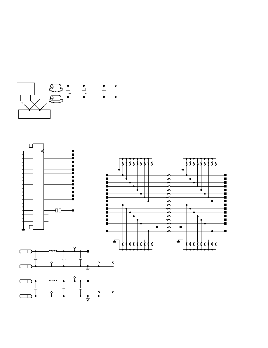
DVDD
DIGITAL
INPUT
Figure 6. Equivalent Digital Input
The digital interface is implemented using an edge-triggered
master/slave latch. The DAC output updates on the rising edge
of the clock and is designed to support a clock rate as high as
165 MSPS. The clock can be operated at any duty cycle that
meets the specified latch pulsewidth. The setup and hold times
can also be varied within the clock cycle as long as the specified
minimum times are met, although the location of these transition
edges may affect digital feedthrough and distortion performance.
Best performance is typically achieved when the input data
transitions on the falling edge of a 50% duty cycle clock.
CLOCK INPUT
SOIC/TSSOP Packages
The 28-lead package options have a single-ended clock input
(CLOCK) that must be driven to rail-to-rail CMOS levels. The
quality of the DAC output is directly related to the clock qual-
ity, and jitter is a key concern. Any noise or jitter in the clock
will translate directly into the DAC output. Optimal perfor-
mance will be achieved if the CLOCK input has a sharp rising
edge, since the DAC latches are positive edge triggered.
LFCSP Package
A configurable clock input is available in the LFCSP package,
which allows for one single-ended and two differential modes. The
mode selection is controlled by the CMODE input, as summa-
rized in Table I. Connecting CMODE to CLKCOM selects the
single-ended clock input. In this mode, the CLK+ input is driven
with rail-to-rail swings and the CLK≠ input is left floating. If
CMODE is connected to CLKVDD, the differential receiver
mode is selected. In this mode, both inputs are high impedance.
The final mode is selected by floating CMODE. This mode is
also differential, but internal terminations for positive emitter-
coupled logic (PECL) are activated. There is no significant
performance difference among any of the three clock input modes.
Table I. Clock Mode Selection
CMODE Pin
Clock Input Mode
CLKCOM
Single-Ended
CLKVDD
Differential
Float
PECL
The single-ended input mode operates in the same way as the
CLOCK input in the 28-lead packages, as described previously.
In the differential input mode, the clock input functions as a
high impedance differential pair. The common-mode level of
the CLK+ and CLK≠ inputs can vary from 0.75 V to 2.25 V,
and the differential voltage can be as low as 0.5 V p-p. This mode
can be used to drive the clock with a differential sine wave since
the high gain bandwidth of the differential inputs will convert
the sine wave into a single-ended square wave internally.
The final clock mode allows for a reduced external component
count when the DAC clock is distributed on the board using
PECL logic. The internal termination configuration is shown in
Figure 7. These termination resistors are untrimmed and can
vary up to
±20%. However, matching between the resistors
should generally be better than
±1%
CLK+
TO DAC CORE
CLK≠
V
TT
= 1.3V NOM
50
50
AD9744
CLOCK
RECEIVER
Figure 7. Clock Termination in PECL Mode
DAC TIMING
Input Clock and Data Timing Relationship
Dynamic performance in a DAC is dependent on the relation-
ship between the position of the clock edges and the time at
REV. A
AD9744
≠13≠
which the input data changes. The AD9744 is rising edge triggered,
and so exhibits dynamic performance sensitivity when the data
transition is close to this edge. In general, the goal when apply-
ing the AD9744 is to make the data transition close to the falling
clock edge. This becomes more important as the sample rate
increases. Figure 8 shows the relationship of SFDR to clock
placement with different sample rates. Note that at the lower
sample rates, more tolerance is allowed in clock placement, while
at higher rates, more care must be taken.
≠3
≠2
2
≠1
0
1
65
75
ns
dB
3
55
45
35
60
70
50
40
50MHz SFDR
20MHz SFDR
50MHz SFDR
Figure 8. SFDR vs. Clock Placement @ f
OUT
= 20 MHz
and 50 MHz
Sleep Mode Operation
The AD9744 has a power-down function that turns off the
output current and reduces the supply current to less than 6 mA
over the specified supply range of 2.7 V to 3.6 V and tempera-
ture range. This mode can be activated by applying a logic level
1 to the SLEEP pin. The SLEEP pin logic threshold is equal to
0.5
• AVDD. This digital input also contains an active pull-
down circuit that ensures that the AD9744 remains enabled if
this input is left disconnected. The AD9744 takes less than
50 ns to power down and approximately 5
ms to power back up.
POWER DISSIPATION
The power dissipation, P
D
, of the AD9744 is dependent on
several factors that include:
The power supply voltages (AVDD, CLKVDD, and DVDD)
The full-scale current output I
OUTFS
The update rate f
CLOCK
The reconstructed digital input waveform
The power dissipation is directly proportional to the analog
supply current, I
AVDD
, and the digital supply current, I
DVDD
.
I
AVDD
is directly proportional to I
OUTFS
, as shown in Figure 9,
and is insensitive to f
CLOCK
. Conversely, I
DVDD
is dependent on
both the digital input waveform, f
CLOCK
, and digital supply
DVDD. Figure 10 shows I
DVDD
as a function of full-scale sine
wave output ratios (f
OUT
/f
CLOCK
) for various update rates with
DVDD = 3.3 V.
I
OUTFS
(mA)
35
0
2
I
AV
D
D
(mA)
30
25
20
15
10
4
6
8
10
12
14
16
18
20
Figure 9. I
AVDD
vs. I
OUTFS
RATIO (
f
OUT
/
f
CLOCK
)
16
0.01
1
0.1
I
DV
D
D
(mA)
14
12
10
8
6
4
2
0
165MSPS
125MSPS
65MSPS
Figure 10. I
DVDD
vs. Ratio @ DVDD = 3.3 V
50
100
150
0
1
2
3
4
5
6
7
8
9
10
f
CLOCK
(MSPS)
I
CLKVDD
(
mA)
200
0
DIFF
PECL
SE
Figure 11. I
CLKVDD
vs. f
CLOCK
and Clock Mode
REV. A
≠14≠
AD9744
APPLYING THE AD9744
Output Configurations
The following sections illustrate some typical output configura-
tions for the AD9744. Unless otherwise noted, it is assumed
that I
OUTFS
is set to a nominal 20 mA. For applications requir-
ing the optimum dynamic performance, a differential output
configuration is suggested. A differential output configuration
may consist of either an RF transformer or a differential op amp
configuration. The transformer configuration provides the opti-
mum high frequency performance and is recommended for any
application that allows ac coupling. The differential op amp
configuration is suitable for applications requiring dc coupling,
a bipolar output, signal gain, and/or level shifting within the
bandwidth of the chosen op amp.
A single-ended output is suitable for applications requiring a
unipolar voltage output. A positive unipolar output voltage will
result if IOUTA and/or IOUTB is connected to an appropriately
sized load resistor, R
LOAD
, referred to ACOM. This configura-
tion may be more suitable for a single-supply system requiring a
dc-coupled, ground referred output voltage. Alternatively, an
amplifier could be configured as an I-V converter, thus convert-
ing IOUTA or IOUTB into a negative unipolar voltage. This
configuration provides the best dc linearity since IOUTA or
IOUTB is maintained at a virtual ground.
DIFFERENTIAL COUPLING USING A TRANSFORMER
An RF transformer can be used to perform a differential-to-single-
ended signal conversion, as shown in Figure 12. A differentially
coupled transformer output provides the optimum distortion
performance for output signals whose spectral content lies within
the transformer's pass band. An RF transformer, such as the
Mini-Circuits T1≠1T, provides excellent rejection of common-
mode distortion (i.e., even-order harmonics) and noise over a
wide frequency range. It also provides electrical isolation and the
ability to deliver twice the power to the load. Transformers with
different impedance ratios may also be used for impedance match-
ing purposes. Note that the transformer provides ac coupling only.
R
LOAD
AD9744
22
21
MINI-CIRCUITS
T1-1T
OPTIONAL R
DIFF
IOUTA
IOUTB
Figure 12. Differential Output Using a Transformer
The center tap on the primary side of the transformer must be
connected to ACOM to provide the necessary dc current path
for both IOUTA and IOUTB. The complementary voltages
appearing at IOUTA and IOUTB (i.e., V
OUTA
and V
OUTB
)
swing symmetrically around ACOM and should be maintained
with the specified output compliance range of the AD9744. A
differential resistor, R
DIFF
, may be inserted in applications where
the output of the transformer is connected to the load, R
LOAD
,
via a passive reconstruction filter or cable. R
DIFF
is determined
by the transformer's impedance ratio and provides the proper
source termination that results in a low VSWR. Note that approxi-
mately half the signal power will be dissipated across R
DIFF
.
DIFFERENTIAL COUPLING USING AN OP AMP
An op amp can also be used to perform a differential-to-single-
ended conversion, as shown in Figure 13. The AD9744 is
configured with two equal load resistors, R
LOAD
, of 25
W. The
differential voltage developed across IOUTA and IOUTB is conver-
ted to a single-ended signal via the differential op amp configuration.
An optional capacitor can be installed across IOUTA and IOUTB,
forming a real pole in a low-pass filter. The addition of this
capacitor also enhances the op amp's distortion performance by
preventing the DAC's high slewing output from overloading the
op amp's input.
AD9744
22
IOUTA
IOUTB
21
C
OPT
500
225
225
500
25
25
AD8047
Figure 13. DC Differential Coupling Using an Op Amp
The common-mode rejection of this configuration is typically
determined by the resistor matching. In this circuit, the differ-
ential op amp circuit using the AD8047 is configured to provide
some additional signal gain. The op amp must operate off a dual
supply since its output is approximately
±1 V. A high speed
amplifier capable of preserving the differential performance of the
AD9744 while meeting other system level objectives (e.g., cost
or power) should be selected. The op amp's differential gain, gain
setting resistor values, and full-scale output swing capabilities
should all be considered when optimizing this circuit.
The differential circuit shown in Figure 14 provides the neces-
sary level shifting required in a single-supply system. In this case,
AVDD, which is the positive analog supply for both the AD9744
and the op amp, is also used to level-shift the differential output
of the AD9744 to midsupply (i.e., AVDD/2). The AD8041 is a
suitable op amp for this application.
AD9744
22
IOUTA
IOUTB
21
C
OPT
500
225
225
1k
25
25
AD8041
1k
AVDD
Figure 14. Single Supply DC Differential Coupled Circuit
SINGLE-ENDED UNBUFFERED VOLTAGE OUTPUT
Figure 15 shows the AD9744 configured to provide a unipolar
output range of approximately 0 V to 0.5 V for a doubly termi-
nated 50
W cable since the nominal full-scale current, I
OUTFS
, of
20 mA flows through the equivalent R
LOAD
of 25
W. In this case,
R
LOAD
represents the equivalent load resistance seen by IOUTA
or IOUTB. The unused output (IOUTA or IOUTB) can be
connected to ACOM directly or via a matching R
LOAD
. Different
REV. A
AD9744
≠15≠
values of I
OUTFS
and R
LOAD
can be selected as long as the positive
compliance range is adhered to. One additional consideration in
this mode is the integral nonlinearity (INL), discussed in the
Analog Output section. For optimum INL performance, the
single-ended, buffered voltage output configuration is suggested.
AD9744
IOUTA
IOUTB
21
50
25
50
V
OUTA
= 0V TO 0.5V
I
OUTFS
= 20mA
22
Figure 15. 0 V to 0.5 V Unbuffered Voltage Output
SINGLE-ENDED, BUFFERED VOLTAGE OUTPUT
CONFIGURATION
Figure 16 shows a buffered single-ended output configuration in
which the op amp U1 performs an I-V conversion on the AD9744
output current. U1 maintains IOUTA (or IOUTB) at a virtual
ground, minimizing the nonlinear output impedance effect on
the DAC's INL performance as described in the Analog Output
section. Although this single-ended configuration typically provides
the best dc linearity performance, its ac distortion performance
at higher DAC update rates may be limited by U1's slew rate
capabilities. U1 provides a negative unipolar output voltage, and
its full-scale output voltage is simply the product of R
FB
and
I
OUTFS
. The full-scale output should be set within U1's voltage
output swing capabilities by scaling I
OUTFS
and/or R
FB
. An
improvement in ac distortion performance may result with a
reduced I
OUTFS
since the signal current U1 will be required to
sink less signal current.
AD9744
22
IOUTA
IOUTB
21
C
OPT
200
U1
V
OUT
= I
OUTFS
R
FB
I
OUTFS
= 10mA
R
FB
200
Figure 16. Unipolar Buffered Voltage Output
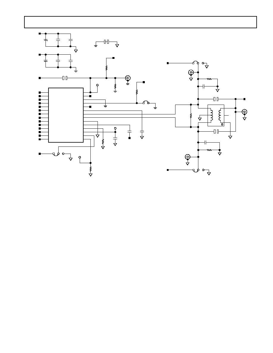
POWER AND GROUNDING CONSIDERATIONS, POWER
SUPPLY REJECTION
Many applications seek high speed and high performance under
less than ideal operating conditions. In these application circuits,
the implementation and construction of the printed circuit board
is as important as the circuit design. Proper RF techniques must
be used for device selection, placement, and routing as well as
power supply bypassing and grounding to ensure optimum per-
formance. Figures 21 to 24 illustrate the recommended printed
circuit board ground, power, and signal plane layouts implemented
on the AD9744 evaluation board.
One factor that can measurably affect system performance is the
ability of the DAC output to reject dc variations or ac noise
superimposed on the analog or digital dc power distribution.
This is referred to as the power supply rejection ratio (PSRR).
For dc variations of the power supply, the resulting performance
of the DAC directly corresponds to a gain error associated
with the DAC's full-scale current, I
OUTFS
. AC noise on the dc
supplies is common in applications where the power distribution
is generated by a switching power supply. Typically, switching
power supply noise will occur over the spectrum from tens of
kHz to several MHz. The PSRR versus frequency of the AD9744
AVDD supply over this frequency range is shown in Figure 17.
FREQUENCY (MHz)
85
40
12
6
0
PSRR (dB)
80
75
70
65
60
55
50
2
4
8
10
45
Figure 17. Power Supply Rejection Ratio (PSRR)
Note that the ratio in Figure 17 is calculated as amps out/volts in.
Noise on the analog power supply has the effect of modulating
the internal switches, and therefore the output current. The
voltage noise on AVDD, therefore, will be added in a nonlinear
manner to the desired IOUT. Due to the relative different size
of these switches, the PSRR is very code dependent. This can
produce a mixing effect that can modulate low frequency power
supply noise to higher frequencies. Worst-case PSRR for either
one of the differential DAC outputs will occur when the full-scale
current is directed toward that output. As a result, the PSRR
measurement in Figure 17 represents a worst-case condition in
which the digital inputs remain static and the full-scale output
current of 20 mA is directed to the DAC output being measured.
An example serves to illustrate the effect of supply noise on the
analog supply. Suppose a switching regulator with a switch-
ing frequency of 250 kHz produces 10 mV of noise and, for
simplicity's sake (ignoring harmonics), all of this noise is con-
centrated at 250 kHz. To calculate how much of this undesired
noise will appear as current noise superimposed on the DAC's
full-scale current, I
OUTFS
, one must determine the PSRR in dB
using Figure 17 at 250 kHz. To calculate the PSRR for a given
R
LOAD
, such that the units of PSRR are converted from A/V to
V/V, adjust the curve in Figure 17 by the scaling factor 20
• log
(R
LOAD
). For instance, if R
LOAD
is 50
W, the PSRR is reduced by
34 dB (i.e., PSRR of the DAC at 250 kHz, which is 85 dB in
Figure 17, becomes 51 dB V
OUT
/V
IN
).
Proper grounding and decoupling should be a primary objec-
tive in any high speed, high resolution system. The AD9744
features separate analog and digital supplies and ground pins to
optimize the management of analog and digital ground currents
in a system. In general, AVDD, the analog supply, should be
decoupled to ACOM, the analog common, as close to the chip
REV. A
≠16≠
AD9744
2
R1
3
R2
4
R3
5
R4
6
R5
7
R6
8
R7
9
R8
10
R9
RP5
OPT
1
DCOM
16
1 RP3
22
DB13
DB12
DB11
DB10
DB9
DB8
DB7
DB6
DB5
DB4
DB3
DB2
DB1
DB0
DB13X
DB12X
DB11X
DB10X
DB9X
DB8X
DB7X
DB6X
DB5X
DB4X
DB3X
DB2X
DB1X
DB0X
15
2 RP3
22
14
3 RP3
22
13
4 RP3
22
12
5 RP3
22
11
6 RP3
22
10
7 RP3
22
9
8 RP3
22
16
1 RP4
22
15
2 RP4
22
14
3 RP4
22
13
4 RP4
22
12
5 RP4
22
11
6 RP4
22
9
8 RP4
22
10
7 RP4
22
CKEXT
CKEXTX
2
R1
3
R2
4
R3
5
R4
6
R5
7
R6
8
R7
9
R8
10
R9
RP6
OPT
1
DCOM
2
R1
3
R2
4
R3
5
R4
6
R5
7
R6
8
R7
9
R8
10
R9
RP1
OPT
1
DCOM
2
R1
3
R2
4
R3
5
R4
6
R5
7
R6
8
R7
9
R8
10
R9
RP2
OPT
1
DCOM
2
1
DB13X
4
3
DB12X
6
5
DB11X
8
7
DB10X
10
9
DB9X
12
11
DB8X
14
13
DB7X
16
15
DB6X
18
17
DB5X
20
19
DB4X
22
21
DB3X
24
23
DB2X
26
25
DB1X
28
27
DB0X
30
29
32
31
34
33
CKEXTX
36
35
38
37
40
39
JP3
J1
RIBBON
TB1 1
TB1 2
L2
BEAD
C7
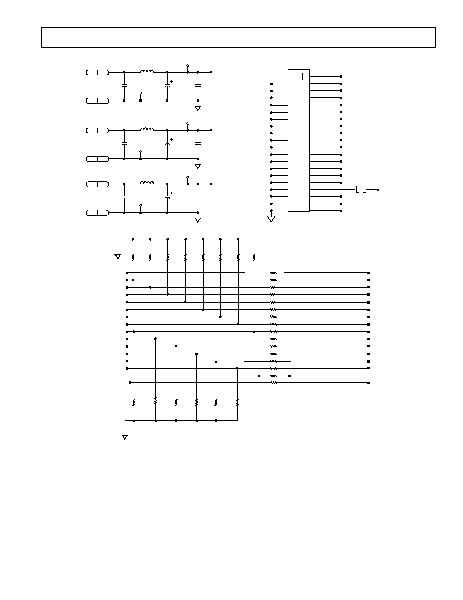
0.1 F
TP4
BLK
+
DVDD
TP7
C6
0.1 F
C4
10 F
25V
BLK
BLK
TP8
TP2
RED
TB1 3
TB1 4
L3
BEAD
C9
0.1 F
TP6
BLK
+
AVDD
TP10
C8
0.1 F
C5
10 F
25V
BLK
BLK
TP9
TP5
RED
Figure 19. SOIC Evaluation Board--Power Supply and Digital Inputs
as physically possible. Similarly, DVDD, the digital supply, should
be decoupled to DCOM as close to the chip as physically possible.
For those applications that require a single 3.3 V supply for both
the analog and digital supplies, a clean analog supply may be
generated using the circuit shown in Figure 18. The circuit
consists of a differential LC filter with separate power supply
and return lines. Lower noise can be attained by using low ESR
type electrolytic and tantalum capacitors.
100 F
ELECT.
0.1 F
CER.
TTL/CMOS
LOGIC
CIRCUITS
3.3V
POWER SUPPLY
FERRITE
BEADS
AVDD
ACOM
10 F≠22 F
TANT.
Figure 18. Differential LC Filter for Single 3.3 V Applications
EVALUATION BOARD
General Description
The TxDAC family evaluation boards allow for easy setup and
testing of any TxDAC product in the SOIC and LFCSP
packages. Careful attention to layout and circuit design, com-
bined with a prototyping area, allows the user to evaluate the
AD9744 easily and effectively in any application where high
resolution, high speed conversion is required.
This board allows the user the flexibility to operate the AD9744
in various configurations. Possible output configurations include
transformer coupled, resistor terminated, and single and differ-
ential outputs. The digital inputs are designed to be driven from
various word generators, with the on-board option to add a
resistor network for proper load termination. Provisions are also
made to operate the AD9744 with either the internal or external
reference or to exercise the power-down feature.
REV. A
AD9744
≠17≠
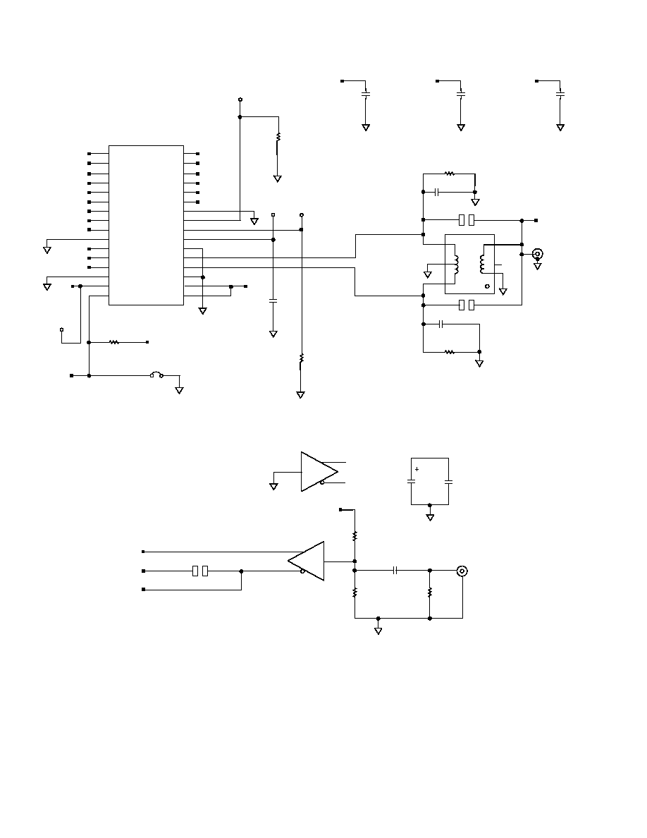
R6
OPT
S2
IOUTA
2
A
B
JP10
1
3
IX
R11
50
C13
OPT
JP8
IOUT
S3
4
5
6
3
2
1
T1
T1-1T
JP9
C12
OPT
R10
50
S1
IOUTB
1
2
3
A
B
JP11
IY
1
EXT
2
3
INT
A
B
JP5
REF
+
+
C14
10 F
16V
C16
0.1 F
C17
0.1 F
AVDD
DVDD
CKEXT
DB13
DB12
DB11
DB10
DB9
DB8
DB7
DB6
DB5
DB4
DB3
DB2
DB1
DB0
AVDD
C15
10 F
16V
C18
0.1 F
C19
0.1 F
CUT
UNDER DUT
JP6
JP4
R5
OPT
DVDD
R4
50
CLOCK
S5
CLOCK
TP1
WHT
DVDD
AVDD
DVDD
R2
10k
JP2
MODE
TP3
WHT
REF
C2
0.1 F
C1
0.1 F
C11
0.1 F
R1
2k
28
27
26
25
24
23
22
21
20
19
18
17
16
15
1
2
3
4
5
6
7
8
9
10
11
12
13
14
U1
AD9744
SLEEP
TP11
WHT
R3
10k
CLOCK
DVDD
DCOM
MODE
AVDD
RESERVED
IOUTA
IOUTB
ACOM
NC
FS ADJ
REFIO
REFLO
SLEEP
DB13
DB12
DB11
DB10
DB9
DB8
DB7
DB6
DB5
DB4
DB3
DB2
DB1
DB0
AVDD
Figure 20. SOIC Evaluation Board--Output Signal Conditioning
REV. A
≠18≠
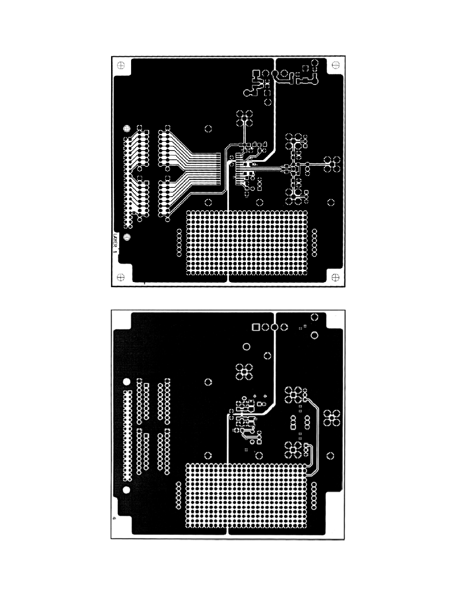
AD9744
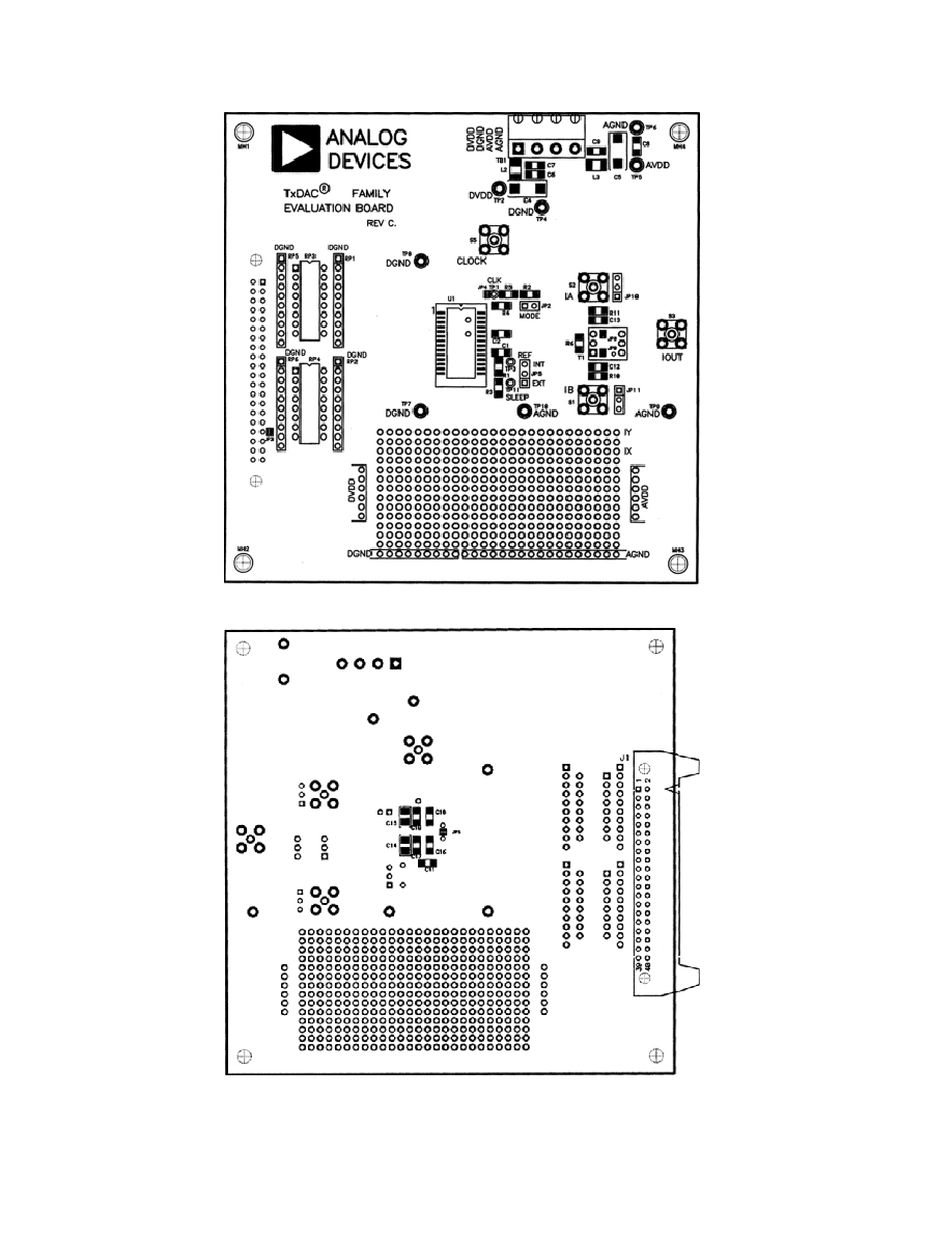
Figure 21. SOIC Evaluation Board≠Primary Side
Figure 22. SOIC Evaluation Board--Secondary Side
REV. A
AD9744
≠19≠
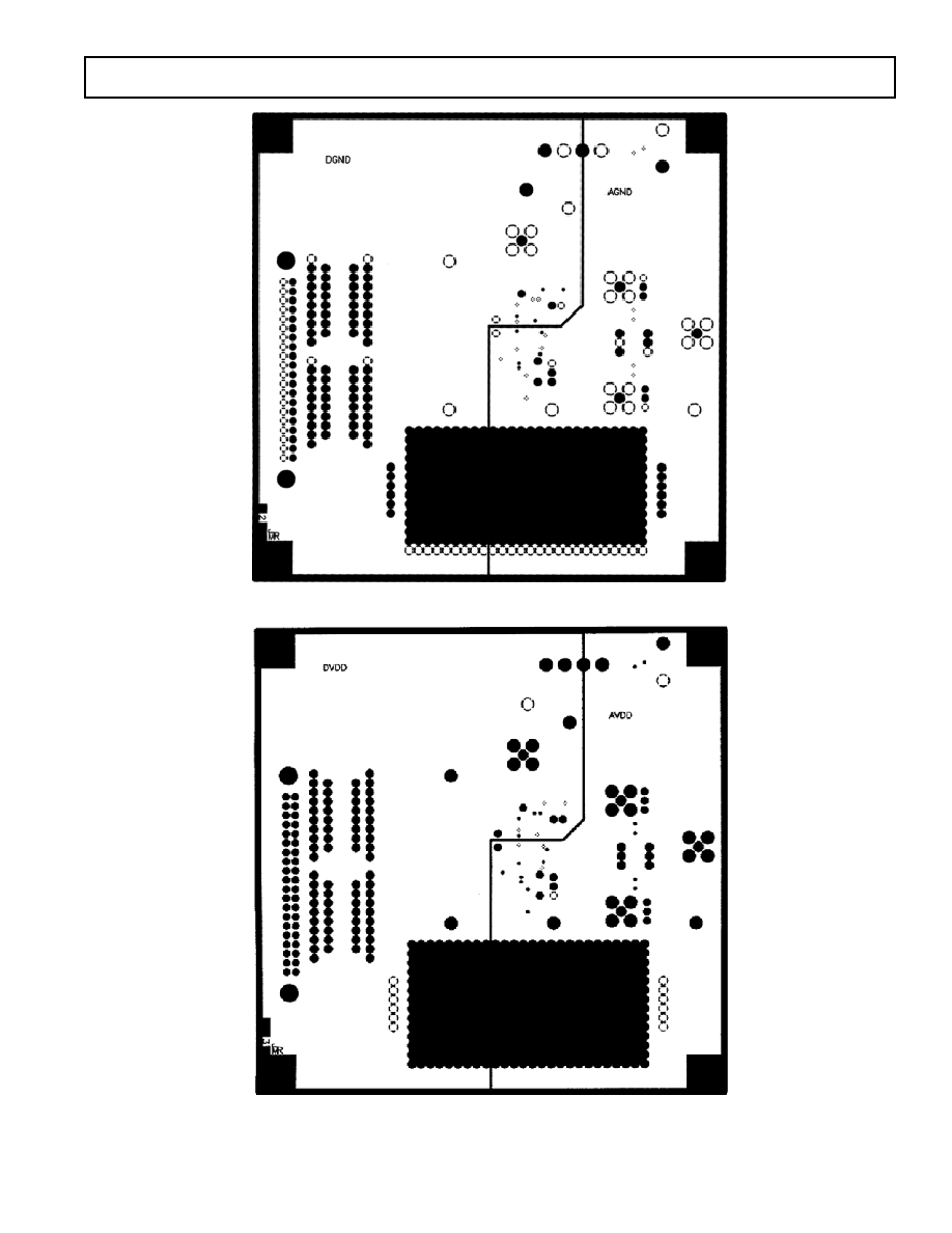
Figure 23. SOIC Evaluation Board≠Ground Plane
Figure 24. SOIC Evaluation Board--Power Plane
REV. A
≠20≠
AD9744
Figure 25. SOIC Evaluation Board Assembly--Primary Side
Figure 26. SOIC Evaluation Board Assembly--Secondary Side
REV. A
AD9744
≠21≠
CVDD
RED
TP12
BEAD
TB1
1
TB1
2
C7
0.1 F
C9
0.1 F
C3
0.1 F
BLK
TP2
TP4
TP6
BLK
BLK
C6
0.1 F
C8
0.1 F
C10
0.1 F
C2
10 F
6.3V
C4
10 F
6.3V
C5
10 F
6.3V
L1
DVDD
RED
TP13
BEAD
TB3
1
TB3
2
L2
AVDD
RED
TP5
BEAD
TB4
1
TB4
2
L3
J1
13
11
9
7
5
3
1
40
38
36
34
32
30
28
26
24
22
20
18
16
14
12
10
8
6
4
2
39
37
35
33
31
29
27
25
23
21
19
17
15
HEADER STRAIGHT UP MALE NO SHROUD
JP3
CKEXTX
CKEXT
CKEXTX
R21
100
R24
100
R25
100
R26
100
R27
100
R28
100
DB0X
DB1X
DB2X
DB3X
DB4X
DB5X
DB6X
DB7X
DB8X
DB9X
DB10X
DB11X
DB12X
DB13X
DB0X
DB1X
DB2X
DB3X
DB4X
DB5X
DB6X
DB7X
DB8X
DB9X
DB10X
DB11X
DB12X
DB13X
DB13
DB12
DB11
DB10
DB9
DB8
DB7
DB6
DB5
DB4
DB3
DB2
DB1
DB0
22
16
22
15
22
14
22
13
22
12
22
11
22
10
22
9
22
16
22
15
22
14
22
13
22
12
22
11
22
10
22
9
R20
100
R19
100
R18
100
R17
100
R16
100
R15
100
R4
100
R3
100
1 RP3
2 RP3
3 RP3
4 RP3
5 RP3
6 RP3
7 RP3
8 RP3
1 RP4
2 RP4
3 RP4
4 RP4
5 RP4
6 RP4
7 RP4
8 RP4
Figure 27. LFCSP Evaluation Board Schematic--Power Supply and Digital Inputs
REV. A
≠22≠
AD9744
CVDD
CVDD
DB8
DB9
DB10
DB11
CLKB
DB5
DVDD
DB6
DB7
CLK
DB0
DB1
DB2
DB3
DB4
DB13
DB12
IOUT
AVDD
DVDD
CVDD
AVDD
DB8
DB9
DB10
DB11
IB
FS ADJ
CLKB
DB5
DVDD
DB6
DB7
CLK
CVDD
DCOM
DB0
DB1
DB2
DB3
DB4
DCOM1
DB13
ACOM1
AVDD
ACOM
IA
REFIO
AVDD1
SLEEP
DB12
CCOM
CMODE
MODE
CMODE
MODE
T1≠1T
T1
JP8
JP9
4
3
2
1
5
6
S3
AGND: 3, 4, 5
R11
50
R10
50
DNP
C13
DNP
C12
28
25
17
23
21
22
18
19
27
26
24
20
29
30
31
32
C11
0.1 F
R1
2k
0.1%
R30
10k
R29
10k
C17
0.1 F
C19
0.1 F
C32
0.1 F
U1
AD9744LFCSP
WHT
TP1
WHT
TP11
JP1
WHT
TP3
TP7
WHT
SLEEP
16
15
14
13
12
11
10
9
8
7
6
5
4
3
2
1
Figure 28. LFCSP Evaluation Board Schematic--Output Signal Conditioning
U4
U4
JP2
AGND: 5
CVDD: 8
4
3
6
CVDD: 8
C35
0.1 F
C20
10 F
16V
S5
AGND: 3, 4, 5
C34
0.1 F
CKEXT
CLK
CLKB
R5
120
R2
120
R6
50
CVDD
AGND: 5
2
1
7
CVDD
Figure 29. LFCSP Evaluation Board Schematic--Clock Input
REV. A
AD9744
≠23≠
Figure 30. LFCSP Evaluation Board Layout--Primary Side
Figure 31. LFCSP Evaluation Board Layout--Secondary Side
REV. A
≠24≠
AD9744
Figure 32. LFCSP Evaluation Board Layout--Ground Plane
Figure 33. LFCSP Evaluation Board Layout--Power Plane
REV. A
AD9744
≠25≠
Figure 34. LFCSP Evaluation Board Layout Assembly--Primary Side
Figure 35. LFCSP Evaluation Board Layout Assembly--Secondary Side
REV. A
≠26≠
AD9744
OUTLINE DIMENSIONS
28-Lead Thin Shrink Small Outline Package [TSSOP]
(RU-28)
Dimensions shown in millimeters
4.50
4.40
4.30
28
15
14
1
9.80
9.70
9.60
6.40 BSC
PIN 1
SEATING
PLANE
0.15
0.05
0.30
0.19
0.65
BSC
1.20
MAX
0.20
0.09
0.75
0.60
0.45
8
0
COMPLIANT TO JEDEC STANDARDS MO-153AE
COPLANARITY
0.10
28-Lead Standard Small Outline Package [SOIC]
Wide Body
(R-28)
Dimensions shown in millimeters and (inches)
CONTROLLING DIMENSIONS ARE IN MILLIMETERS; INCH DIMENSIONS
(IN PARENTHESES) ARE ROUNDED-OFF MILLIMETER EQUIVALENTS FOR
REFERENCE ONLY AND ARE NOT APPROPRIATE FOR USE IN DESIGN
COMPLIANT TO JEDEC STANDARDS MS-013AE
0.32 (0.0126)
0.23 (0.0091)
8
0
0.75 (0.0295)
0.25 (0.0098)
45
1.27 (0.0500)
0.40 (0.0157)
SEATING
PLANE
0.30 (0.0118)
0.10 (0.0039)
0.51 (0.0201)
0.33 (0.0130)
2.65 (0.1043)
2.35 (0.0925)
1.27 (0.0500)
BSC
28
15
14
1
18.10 (0.7126)
17.70 (0.6969)
10.65 (0.4193)
10.00 (0.3937)
7.60 (0.2992)
7.40 (0.2913)
COPLANARITY
0.10
32-Lead Lead Frame Chip Scale Package [LFCSP]
(CP-32)
Dimensions shown in millimeters
COMPLIANT TO JEDEC STANDARDS MO-220-VHHD-2
0.30
0.23
0.18
12
MAX
0.20 REF
0.05 MAX
0.02 NOM
COPLANARITY
0.08
1.00 MAX
0.65 NOM
1.00
0.90
0.80
1
32
8
9
25
24
16
17
BOTTOM
VIEW
0.50
0.40
0.30
3.50
REF
0.50
BSC
PIN 1
INDICATOR
TOP
VIEW
5.00
BSC SQ
4.75
BSC SQ
SQ
3.25
3.10
2.95
PIN 1
INDICATOR
0.60 MAX
0.60 MAX
SEATING
PLANE

REV. A
AD9744
≠27≠
Revision History
Location
Page
5/03--Data Sheet changed from REV. 0 to REV. A.
Added 32-Lead LFCSP Package . . . . . . . . . . . . . . . . . . . . . . . . . . . . . . . . . . . . . . . . . . . . . . . . . . . . . . . . . . . . . . . . . . UNIVERSAL
Edits to FEATURES . . . . . . . . . . . . . . . . . . . . . . . . . . . . . . . . . . . . . . . . . . . . . . . . . . . . . . . . . . . . . . . . . . . . . . . . . . . . . . . . . . . . . 1
Edits to PRODUCT HIGHLIGHTS . . . . . . . . . . . . . . . . . . . . . . . . . . . . . . . . . . . . . . . . . . . . . . . . . . . . . . . . . . . . . . . . . . . . . . . . 1
Edits to DC SPECIFICATIONS . . . . . . . . . . . . . . . . . . . . . . . . . . . . . . . . . . . . . . . . . . . . . . . . . . . . . . . . . . . . . . . . . . . . . . . . . . . 2
Edits to DYNAMIC SPECIFICATIONS . . . . . . . . . . . . . . . . . . . . . . . . . . . . . . . . . . . . . . . . . . . . . . . . . . . . . . . . . . . . . . . . . . . . . 3
Edits to DIGITAL SPECIFICATIONS . . . . . . . . . . . . . . . . . . . . . . . . . . . . . . . . . . . . . . . . . . . . . . . . . . . . . . . . . . . . . . . . . . . . . . 4
Edits to ABSOLUTE MAXIMUM RATINGS . . . . . . . . . . . . . . . . . . . . . . . . . . . . . . . . . . . . . . . . . . . . . . . . . . . . . . . . . . . . . . . . . 5
Edits to THERMAL CHARACTERISTICS . . . . . . . . . . . . . . . . . . . . . . . . . . . . . . . . . . . . . . . . . . . . . . . . . . . . . . . . . . . . . . . . . . . 5
Edits to ORDERING GUIDE . . . . . . . . . . . . . . . . . . . . . . . . . . . . . . . . . . . . . . . . . . . . . . . . . . . . . . . . . . . . . . . . . . . . . . . . . . . . . . 5
Edits to PIN CONFIGURATION . . . . . . . . . . . . . . . . . . . . . . . . . . . . . . . . . . . . . . . . . . . . . . . . . . . . . . . . . . . . . . . . . . . . . . . . . . 6
Edits to PIN FUNCTION DESCRIPTIONS . . . . . . . . . . . . . . . . . . . . . . . . . . . . . . . . . . . . . . . . . . . . . . . . . . . . . . . . . . . . . . . . . . 6
Edits to Figure 2 . . . . . . . . . . . . . . . . . . . . . . . . . . . . . . . . . . . . . . . . . . . . . . . . . . . . . . . . . . . . . . . . . . . . . . . . . . . . . . . . . . . . . . . . 7
Replaced TPCs 1, 4, 7, and 8 . . . . . . . . . . . . . . . . . . . . . . . . . . . . . . . . . . . . . . . . . . . . . . . . . . . . . . . . . . . . . . . . . . . . . . . . . . . . . . 8
Edits to Figure 3 . . . . . . . . . . . . . . . . . . . . . . . . . . . . . . . . . . . . . . . . . . . . . . . . . . . . . . . . . . . . . . . . . . . . . . . . . . . . . . . . . . . . . . . 10
Edits to FUNCTIONAL DESCRIPTION . . . . . . . . . . . . . . . . . . . . . . . . . . . . . . . . . . . . . . . . . . . . . . . . . . . . . . . . . . . . . . . . . . . 10
Added CLOCK INPUT section . . . . . . . . . . . . . . . . . . . . . . . . . . . . . . . . . . . . . . . . . . . . . . . . . . . . . . . . . . . . . . . . . . . . . . . . . . . 12
Added new Figure 7 . . . . . . . . . . . . . . . . . . . . . . . . . . . . . . . . . . . . . . . . . . . . . . . . . . . . . . . . . . . . . . . . . . . . . . . . . . . . . . . . . . . . 12
Edits to DAC TIMING section . . . . . . . . . . . . . . . . . . . . . . . . . . . . . . . . . . . . . . . . . . . . . . . . . . . . . . . . . . . . . . . . . . . . . . . . . . . . 12
Edits to Sleep Mode Operation section . . . . . . . . . . . . . . . . . . . . . . . . . . . . . . . . . . . . . . . . . . . . . . . . . . . . . . . . . . . . . . . . . . . . . . 13
Edits to POWER DISSIPATION section . . . . . . . . . . . . . . . . . . . . . . . . . . . . . . . . . . . . . . . . . . . . . . . . . . . . . . . . . . . . . . . . . . . . 13
Renumbered Figures 8≠26 . . . . . . . . . . . . . . . . . . . . . . . . . . . . . . . . . . . . . . . . . . . . . . . . . . . . . . . . . . . . . . . . . . . . . . . . . . . . . . . . 13
Added Figure 11 . . . . . . . . . . . . . . . . . . . . . . . . . . . . . . . . . . . . . . . . . . . . . . . . . . . . . . . . . . . . . . . . . . . . . . . . . . . . . . . . . . . . . . . 13
Added Figures 27≠35 . . . . . . . . . . . . . . . . . . . . . . . . . . . . . . . . . . . . . . . . . . . . . . . . . . . . . . . . . . . . . . . . . . . . . . . . . . . . . . . . . . . . 21
Updated OUTLINE DIMENSIONS . . . . . . . . . . . . . . . . . . . . . . . . . . . . . . . . . . . . . . . . . . . . . . . . . . . . . . . . . . . . . . . . . . . . . . . 26

C02913≠0≠5/03(A)
≠28≠