Document Outline
- FEATURES
- APPLICATIONS
- FUNCTIONAL BLOCK DIAGRAM
- TABLE OF CONTENTS
- ˛ˇ
- ˛ˇ
- ˛ˇ
- ˛ˇ
- ˛ˇ
- ˛ˇ
- ˛ˇ
- ˛ˇ
- ˛ˇ
400 MSPS 14-Bit, 1.8 V CMOS
Direct Digital Synthesizer
AD9952
Rev. 0
Information furnished by Analog Devices is believed to be accurate and reliable.
However, no responsibility is assumed by Analog Devices for its use, nor for any
infringements of patents or other rights of third parties that may result from its use.
Specifications subject to change without notice. No license is granted by implication
or otherwise under any patent or patent rights of Analog Devices. Trademarks and
registered trademarks are the property of their respective owners.
One Technology Way, P.O. Box 9106, Norwood, MA 02062-9106, U.S.A.
Tel: 781.329.4700
www.analog.com
Fax: 781.326.8703
© 2003 Analog Devices, Inc. All rights reserved.
FEATURES
400 MSPS internal clock speed
Integrated 14-bit DAC
32-bit tuning word
Phase noise ≠120 dBc/Hz @ 1 kHz offset (DAC output)
Excellent dynamic performance
>80 dB SFDR @ 160 MHz (±100 kHz offset) A
OUT
Serial I/O control
1.8 V power supply
Software and hardware controlled power-down
48-lead TQFP/EP package
Support for 5 V input levels on most digital inputs
PLL REFCLK multiplier (4◊ to 20◊)
Internal oscillator, can be driven by a single crystal
Phase modulation capability
Multichip synchronization
High speed comparator (200 MHz toggle rate)
APPLICATIONS
Agile LO frequency synthesis
Programmable clock generators
Test and measurement equipment
Acousto-optic device drivers
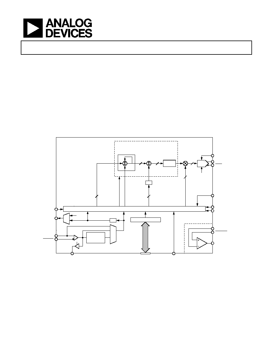
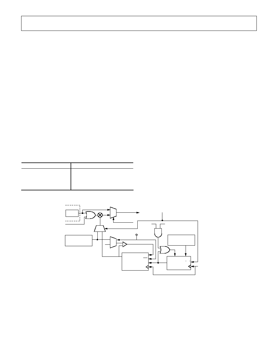
FUNCTIONAL BLOCK DIAGRAM
COS(X)
CONTROL REGISTERS
OSCILLATOR/BUFFER
SYNC
ENABLE
I/O UPDATE
DAC_R
SET
DDS CORE
PHASE
OFFSET
PHASE
ACCUMULATOR
Z
≠1
Z
≠1
IOUT
IOUT
OSK
PWRDWNCTL
REFCLK
REFCLK
CRYSTAL OUT
I/O PORT
DDS
CLOCK
FREQUENCY TUNING WORD
CLE
AR P
HAS
E
ACCUMULATOR
AMP
L
ITUDE
SC
A
L
E FA
C
T
OR
DAC
SYSTEM
CLOCK
SYSTEM
CLOCK
SYNC_IN
SYNC_CLK
RESET
TIMING AND CONTROL LOGIC
4
◊
≠20
◊
CLOCK
MULTIPLIER
˜ 4
AD9952
32
32
14
14
19
14
0
M
U
X
M
U
X
03358-0-001
COMPARATOR
COMP_OUT
COMP_IN
COMP_IN
Figure 1.

AD9952
Rev. 0 | Page 2 of 28
TABLE OF CONTENTS
General Description ......................................................................... 3
AD9952--Electrical Specifications ................................................ 4
Absolute Maximum Ratings............................................................ 7
Pin Configuration............................................................................. 8
Pin Function Descriptions .............................................................. 9
Typical Performance Characteristics ........................................... 10
Theory of Operation ...................................................................... 13
Component Blocks ..................................................................... 13
Modes of Operation ................................................................... 18
Programming AD9952 Features............................................... 18
Serial Port Operation ................................................................. 21
Instruction Byte .......................................................................... 23
Serial Interface Port Pin Description....................................... 23
MSB/LSB Transfers .................................................................... 23
Suggested Application Circuits..................................................... 25
Outline Dimensions ....................................................................... 26
ESD Caution................................................................................ 26
Ordering Guide .......................................................................... 26
REVISION HISTORY
Revision 0: Initial Version

AD9952
Rev. 0 | Page 3 of 28
GENERAL DESCRIPTION
The AD9952 is a direct digital synthesizer (DDS) featuring a
14-bit DAC operating up to 400 MSPS. The AD9952 uses
advanced DDS technology, coupled with an internal high speed,
high performance DAC to form a digitally programmable,
complete high frequency synthesizer capable of generating a
frequency-agile analog output sinusoidal waveform at up to
200 MHz. The AD9952 is designed to provide fast frequency
hopping and fine tuning resolution (32-bit frequency tuning
word). The frequency tuning and control words are loaded into
the AD9952 via a serial I/O port.
The AD9952 is specified to operate over the extended industrial
temperature range of ≠40∞C to +105∞C.

AD9952
Rev. 0 | Page 4 of 28
ELECTRICAL SPECIFICATIONS
Table 1. Unless otherwise noted, AVDD, DVDD = 1.8 V ± 5%, DVDD_I/O = 3.3 V ± 5%, R
SET
= 3.92 k, External Reference Clock
Frequency = 20 MHz with REFCLK Multiplier Enabled at 20◊. DAC Output Must Be Referenced to AVDD, Not AGND.
Parameter Temp
Min
Typ
Max
Unit
REF CLOCK INPUT CHARACTERISTICS
Frequency Range
REFCLK Multiplier Disabled
FULL
1
400
MHz
REFCLK Multiplier Enabled at 4◊
FULL
20
100
MHz
REFCLK Multiplier Enabled at 20◊
FULL
4
20
MHz
Input Capacitance
25∞C
3
pF
Input Impedance
25∞C
1.5
k
Duty Cycle
25∞C
50
%
Duty Cycle with REFCLK Multiplier Enabled
25∞C
35
65
%
REFCLK Input Power
1
FULL
≠15
0
+3
dBm
DAC OUTPUT CHARACTERISTICS
Resolution
14
Bits
Full-Scale Output Current
25∞C
5
10
15
mA
Gain Error
25∞C
≠10
+10
%FS
Output Offset
25∞C
0.6
µA
Differential Nonlinearity
25∞C
1
LSB
Integral Nonlinearity
25∞C
2
LSB
Output Capacitance
25∞C
5
pF
Residual Phase Noise @ 1 kHz Offset, 40 MHz A
OUT
REFCLK Multiplier Enabled @ 20◊
25∞C
≠105
dBc/Hz
REFCLK Multiplier Enabled @ 4◊
25∞C
≠115
dBc/Hz
REFCLK Multiplier Disabled
25∞C
≠132
dBc/Hz
Voltage Compliance Range
25∞C
AVDD ≠ 0.5
AVDD + 0.5
V
Wideband SFDR
1 MHz to 10 MHz Analog Out
25∞C
73
dBc
10 MHz to 40 MHz Analog Out
25∞C
67
dBc
40 MHz to 80 MHz Analog Out
25∞C
62
dBc
80 MHz to 120 MHz Analog Out
25∞C
58
dBc
120 MHz to 160 MHz Analog Out
25∞C
52
dBc
Narrow-Band SFDR
40 MHz Analog Out (±1 MHz)
25∞C
87
dBc
40 MHz Analog Out (±250 kHz)
25∞C
89
dBc
40 MHz Analog Out (±50 kHz)
25∞C
91
dBc
40 MHz Analog Out (±10 kHz)
25∞C
93
dBc
80 MHz Analog Out (±1 MHz)
25∞C
85
dBc
80 MHz Analog Out (±250 kHz)
25∞C
87
dBc
80 MHz Analog Out (±50 kHz)
25∞C
89
dBc
80 MHz Analog Out (±10 kHz)
25∞C
91
dBc
120 MHz Analog Out (±1 MHz)
25∞C
83
dBc
120 MHz Analog Out (±250 kHz)
25∞C
85
dBc
120 MHz Analog Out (±50 kHz)
25∞C
87
dBc
120 MHz Analog Out (±10 kHz)
25∞C
89
dBc
160 MHz Analog Out (±1 MHz)
25∞C
81
dBc
160 MHz Analog Out (±250 kHz)
25∞C
83
dBc
160 MHz Analog Out (±50 kHz)
25∞C
85
dBc
160 MHz Analog Out (±10 kHz)
25∞C
87
dBc

AD9952
Rev. 0 | Page 5 of 28
Parameter Temp
Min
Typ
Max
Unit
COMPARATOR INPUT CHARACTERISTICS
Input Capacitance
25∞C
3
pF
Input Resistance
25∞C
500
k
Input Current
25∞C
±12
µA
Hysteresis 25∞C
30
45
mA
COMPARATOR OUTPUT CHARACTERISTICS
Logic 1 Voltage, High Z Load
FULL
1.6
V
Logic 0 Voltage, High Z Load
FULL
0.4
V
Propagation Delay
25∞C
3
ns
Output Duty Cycle Error
25∞C
±5
%
Rise/Fall Time, 5 pF Load
25∞C
1
ns
Toggle Rate, High Z Load
25∞C
200
MHz
Output Jitter
2
25∞C
1
ps
rms
COMPARATOR NARROW-BAND SFDR
10 MHz (1 MHz)
25∞C
80
dBc
10 MHz (250 kHz)
25∞C
85
dBc
10 MHz (50 kHz)
25∞C
90
dBc
10 MHz (10 kHz)
25∞C
95
dBc
70 MHz (1 MHz)
25∞C
80
dBc
70 MHz (250 kHz)
25∞C
85
dBc
70 MHz (50 kHz)
25∞C
90
dBc
70 MHz (10 kHz)
25∞C
95
dBc
110 MHz (1 MHz)
25∞C
80
dBc
110 MHz (250 kHz)
25∞C
85
dBc
110 MHz (50 kHz)
25∞C
90
dBc
110 MHz (10 kHz)
25∞C
95
dBc
140 MHz (1 MHz)
25∞C
80
dBc
140 MHz (250 kHz)
25∞C
85
dBc
140 MHz (50 kHz)
25∞C
90
dBc
140 MHz (10 kHz)
25∞C
95
dBc
160 MHz (1 MHz)
25∞C
80
dBc
160 MHz (250 kHz)
25∞C
85
dBc
160 MHz (50 kHz)
25∞C
90
dBc
160 MHz (10 kHz)
25∞C
95
dBc
CLOCK GENERATOR OUTPUT JITTER
3
5 MHz A
OUT
25∞C
100
ps rms
10 MHz A
OUT
25∞C
60
ps
rms
40 MHz A
OUT
25∞C
50
ps
rms
80 MHz A
OUT
25∞C
50
ps
rms
120 MHz A
OUT
25∞C
50
ps
rms
140 MHz A
OUT
25∞C
50
ps
rms
160 MHz A
OUT
25∞C
50
ps
rms
TIMING CHARACTERISTICS
Serial Control Bus
Maximum Frequency
FULL
25
Mbps
Minimum Clock Pulse Width Low
FULL
7
ns
Minimum Clock Pulse Width High
FULL
7
ns
Maximum Clock Rise/Fall Time
FULL
2
ns
Minimum Data Setup Time DVDD_I/O = 3.3 V
FULL
3
ns
Minimum Data Setup Time DVDD_I/O = 1.8 V
FULL
5
ns
Minimum Data Hold Time
FULL
0
ns
Maximum Data Valid Time
FULL
25
ns

AD9952
Rev. 0 | Page 6 of 28
Parameter Temp
Min
Typ
Max
Unit
Wake-Up Time
4
FULL
1
ms
Minimum Reset Pulse Width High
FULL
5
SYSCLK Cycles
5
I/O UPDATE to SYNC_CLK Setup Time DVDD_I/O = 3.3 V
FULL
4
ns
I/O UPDATE to SYNC_CLK Setup Time DVDD_I/O = 3.3 V
FULL
6
ns
I/O UPDATE, SYNC_CLK Hold Time
FULL
0
ns
Latency
I/O UPDATE to Frequency Change Prop Delay
25∞C
24
SYSCLK Cycles
I/O UPDATE to Phase Offset Change Prop Delay
25∞C
24
SYSCLK Cycles
I/O UPDATE to Amplitude Change Prop Delay
25∞C
16
SYSCLK Cycles
CMOS LOGIC INPUTS
Logic 1 Voltage @ DVDD_I/O (Pin 43) = 1.8 V
25∞C
1.25
V
Logic 0 Voltage @ DVDD_I/O (Pin 43) = 1.8 V
25∞C
0.6
V
Logic 1 Voltage @ DVDD_I/O (Pin 43) = 3.3 V
25∞C
2.2
V
Logic 0 Voltage @ DVDD_I/O (Pin 43) = 3.3 V
25∞C
0.8
V
Logic 1 Current
25∞C
3
12
µA
Logic 0 Current
25∞C
12
µA
Input Capacitance
25∞C
2
pF
CMOS LOGIC OUTPUTS (1 mA Load) DVDD_I/O = 1.8 V
Logic 1 Voltage
25∞C
1.35
V
Logic 0 Voltage
25∞C
0.4
V
CMOS LOGIC OUTPUTS (1 mA Load) DVDD_I/O = 3.3 V
Logic 1 Voltage
25∞C
2.8
V
Logic 0 Voltage
25∞C
0.4
V
POWER CONSUMPTION (AVDD = DVDD = 1.8 V)
Single-Tone Mode
25∞C
162
171
mW
Rapid Power-Down Mode
25∞C
150
160
mW
Full-Sleep Mode
25∞C
20
27
mW
SYNCHRONIZATION FUNCTION
6
Maximum SYNC Clock Rate (DVDD_I/O = 1.8 V)
25∞C
62.5
MHz
Maximum SYNC Clock Rate (DVDD_I/O = 3.3 V)
25∞C
100
MHz
SYNC_CLK Alignment Resolution
7
25∞C
±1
SYSCLK
Cycles
1
To achieve the best possible phase noise, the largest amplitude clock possible should be used. Reducing the clock input amplitude will reduce the phase noise
performance of the device.
2
Represents the cycle-to-cycle residual jitter from the comparator alone.
3
Represents the cycle-to-cycle residual jitter from the DDS core driving the comparator.
4
Wake-up time refers to the recovery from analog power-down modes (see the Power-Down Functions of the AD9952 section). The longest time required is for the
reference clock multiplier PLL to relock to the reference. The wake-up time assumes there is no capacitor on DACBP and that the recommended PLL loop filter values
are used.
5
SYSCLK cycle refers to the actual clock frequency used on-chip by the DDS. If the reference clock multiplier is used to multiply the external reference clock frequency,
the SYSCLK frequency is the external frequency multiplied by the reference clock multiplication factor. If the reference clock multiplier is not used, the SYSCLK
frequency is the same as the external reference clock frequency.
6
SYNC_CLK = º SYSCLK rate. For SYNC_CLK rates
50 MHz, the high speed sync enable bit, CFR2<11>, should be set.
7
This parameter indicates that the digital synchronization feature cannot overcome phase delays (timing skew) between system clock rising edges. If the system clock
edges are aligned, the synchronization function should not increase the skew between the two edges.
AD9952
Rev. 0 | Page 7 of 28
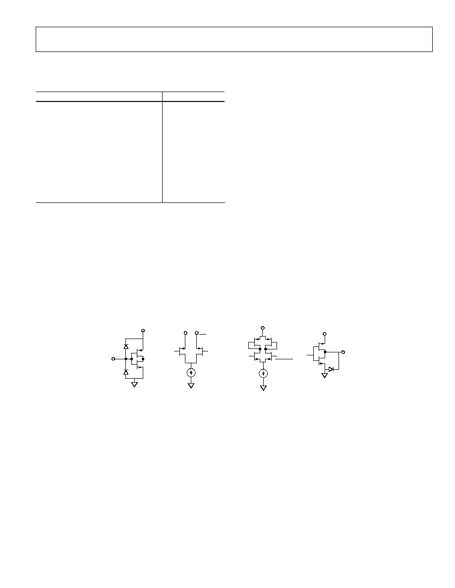
ABSOLUTE MAXIMUM RATINGS
Table 2.
Parameter Rating
Maximum Junction Temperature
150∞C
DVDD_I/O (Pin 43)
4 V
AVDD, DVDD
2 V
Digital Input Voltage (DVDD_I/O = 3.3 V)
≠0.7 V to +5.25 V
Digital Input Voltage (DVDD_I/O = 1.8 V)
≠0.7 V to +2.2 V
Digital Output Current
5 mA
Storage Temperature
≠65∞C to +150∞C
Operating Temperature
≠40∞C to +105∞C
Lead Temperature (10 sec Soldering)
300∞C
JA
38∞C/W
JC
15∞C/W
Stresses above those listed under Absolute Maximum Ratings
may cause permanent damage to the device. This is a stress
rating only and functional operation of the device at these or
any other conditions above those indicated in the operational
section of this specification is not implied. Exposure to absolute
maximum rating conditions for extended periods may affect
device reliability.
03
3
7
4-
0-
03
2
IOUT
IOUT
MUST TERMINATE
OUTPUTS TO AVDD FOR
CURRENT FLOW. DO
NOT EXCEED THE
OUTPUT VOLTAGE
COMPLIANCE RATING.
DAC OUTPUTS
AVDD
COMPARATOR
OUTPUT
DVDD_I/O
INPUT
DIGITAL
INPUTS
AVOID OVERDRIVING
DIGITAL INPUTS.
FORWARD BIASING
ESD DIODES MAY
COUPLE DIGITAL NOISE
ONTO POWER PINS.
AVDD
COMP IN
COMP IN
COMPARATOR
INPUTS
Figure 2. Equivalent Input and Output Circuits
AD9952
Rev. 0 | Page 8 of 28
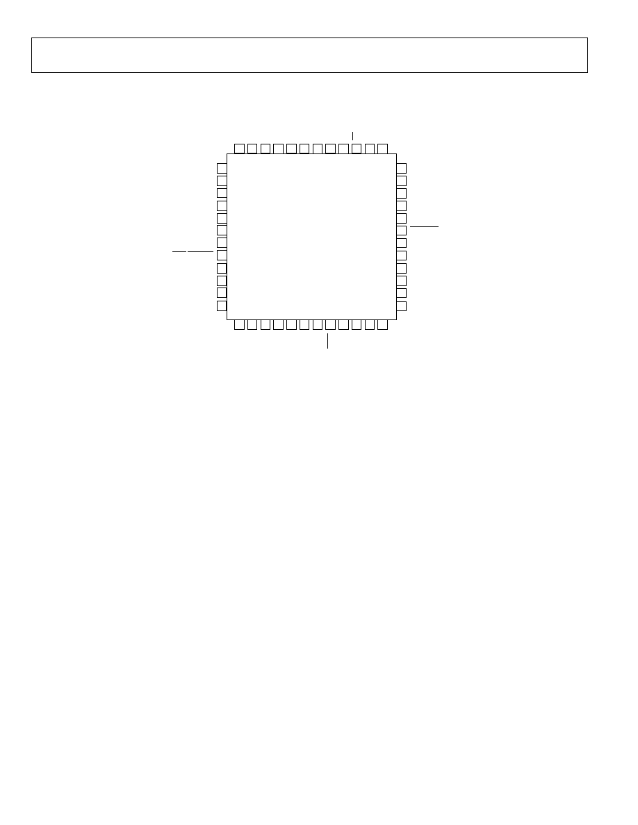
PIN CONFIGURATION
43
42
41
40
39
38
37
48
47
46
45
44
13
15
16
17
18
19
20
21
22
23
24
I/O UPDATE
DVDD
DGND
AVDD
AGND
AVDD
AGND
OSC/REFCLK
OSC/REFCLK
CRYSTAL OUT
CLKMODESELECT
LOOP_FILTER
AGND
AV
DD
AGND
AV
DD
AGND
AV
DD
IOUT
AV
DD
IOUT
DACBP
AGND
OSK
DV
DD
DV
DD
S
Y
NC_
CL
K
S
Y
NC_
IN
DV
DD_
I/O
SC
LK
DGND
SD
IO
SD
O
CS
IOSYN
C
RESET
PWRDWNCTL
DVDD
DGND
AGND
COMP_IN
COMP_IN
AVDD
COMP_OUT
AVDD
AGND
AVDD
AD9952
TOP VIEW
(Not to Scale)
14
1
2
3
4
5
6
7
8
9
10
11
12
36
35
34
33
32
31
30
29
28
27
26
25
03358-0-002
DAC_
R
SET
Figure 3. 48-Lead TQFP/EP
Note that the exposed paddle on the bottom of the package forms an electrical connection for the DAC and must be attached to
analog ground. Note that Pin 43, DVDD_I/O, can be powered to 1.8 V or 3.3 V; however, the DVDD pins (Pin 2 and Pin 34) can only
be powered to 1.8 V.
AD9952
Rev. 0 | Page 9 of 28
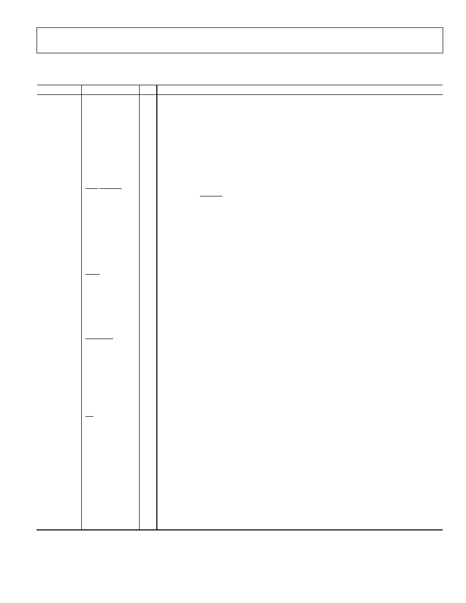
PIN FUNCTION DESCRIPTIONS
Table 3. 48-Lead TQFP/EP
Pin No.
Mnemonic
I/O
Description
1 I/O
UPDATE
I
The rising edge transfers the contents of the internal buffer memory to the I/O registers. This pin
must be set up and held around the SYNC_CLK output signal.
2, 34
DVDD
I
Digital Power Supply Pins (1.8 V).
3, 33, 42,
47, 48
DGND
I
Digital Power Ground Pins.
4, 6, 13,
16, 18, 19,
25, 27, 29
AVDD
I
Analog Power Supply Pins (1.8 V).
5, 7, 14,
15, 17, 22,
26, 32
AGND
I
Analog Power Ground Pins.
8
OSC/REFCLK
I
Complementary Reference Clock/Oscillator Input. When the REFCLK port is operated in single-
ended mode, REFCLK should be decoupled to AVDD with a 0.1 µF capacitor.
9 OSC/REFCLK
I
Reference Clock/Oscillator Input. See Clock Input section for details on the OSCILLATOR/REFCLK
operation.
10
CRYSTAL OUT
O
Output of the Oscillator Section.
11 CLKMODESELECT
I
Control Pin for the Oscillator Section. When high, the oscillator section is enabled. When low, the
oscillator section is bypassed.
12 LOOP_FILTER
I
This pin provides the connection for the external zero compensation network of the REFCLK
multiplier's PLL loop filter. The network consists of a 1 k resistor in series with a 0.1 µF capacitor
tied to AVDD.
20
IOUT
O
Complementary DAC Output. Should be biased through a resistor to AVDD, not AGND.
21
IOUT
O
DAC Output. Should be biased through a resistor to AVDD, not AGND.
23
DACBP
I
DAC Biasline Decoupling Pin.
24 DAC_R
SET
I
A resistor (3.92 k nominal) connected from AGND to DAC_R
SET
establishes the reference current
for the DAC.
28 COMP_OUT
O
Comparator
Output.
30 COMP_IN
I
Compator
Input.
31
COMP_IN
I
Compartor Complementary Input
35
PWRDWNCTL
I
Input Pin Used as an External Power-Down Control (see Table 8 for details).
36 RESET I
Active High Hardware Reset Pin. Assertion of the RESET pin forces the AD9952 to the initial state,
as described in the I/O port register map.
37 IOSYNC I
Asynchronous Active High Reset of the Serial Port Controller. When high, the current I/O
operation is immediately terminated, enabling a new I/O operation to commence once IOSYNC is
returned low. If unused, ground this pin; do not allow this pin to float.
38 SDO
O
When operating the I/O port as a 3-wire serial port, this pin serves as the serial data output. When
operated as a 2-wire serial port, this pin is unused and can be left unconnected.
39
CS
I
This pin functions as an active low chip select that allows multiple devices to share the I/O bus.
40
SCLK
I
This pin functions as the serial data clock for I/O operations.
41 SDIO
I/O
When operating the I/O port as a 3-wire serial port, this pin serves as the serial data input only.
When operated as a 2-wire serial port, this pin is the bidirectional serial data pin.
43
DVDD_I/O
I
Digital Power Supply (for I/O Cells Only, 3.3 V).
44 SYNC_IN
I
Input Signal Used to Synchronize Multiple AD9952s. This input is connected to the SYNC_CLK
output of a master AD9952.
45
SYNC_CLK
O
Clock Output Pin that Serves as a Synchronizer for External Hardware.
46 OSK
I
Input Pin Used to Control the Direction of the Shaped On-Off Keying Function when
Programmed for Operation. OSK is synchronous to the SYNC_CLK pin. When OSK is not
programmed, this pin should be tied to DGND.
<49> AGND
I
The exposed paddle on the bottom of the package is a ground connection for the DAC and must
be attached to AGND in any board layout.
AD9952
Rev. 0 | Page 10 of 28
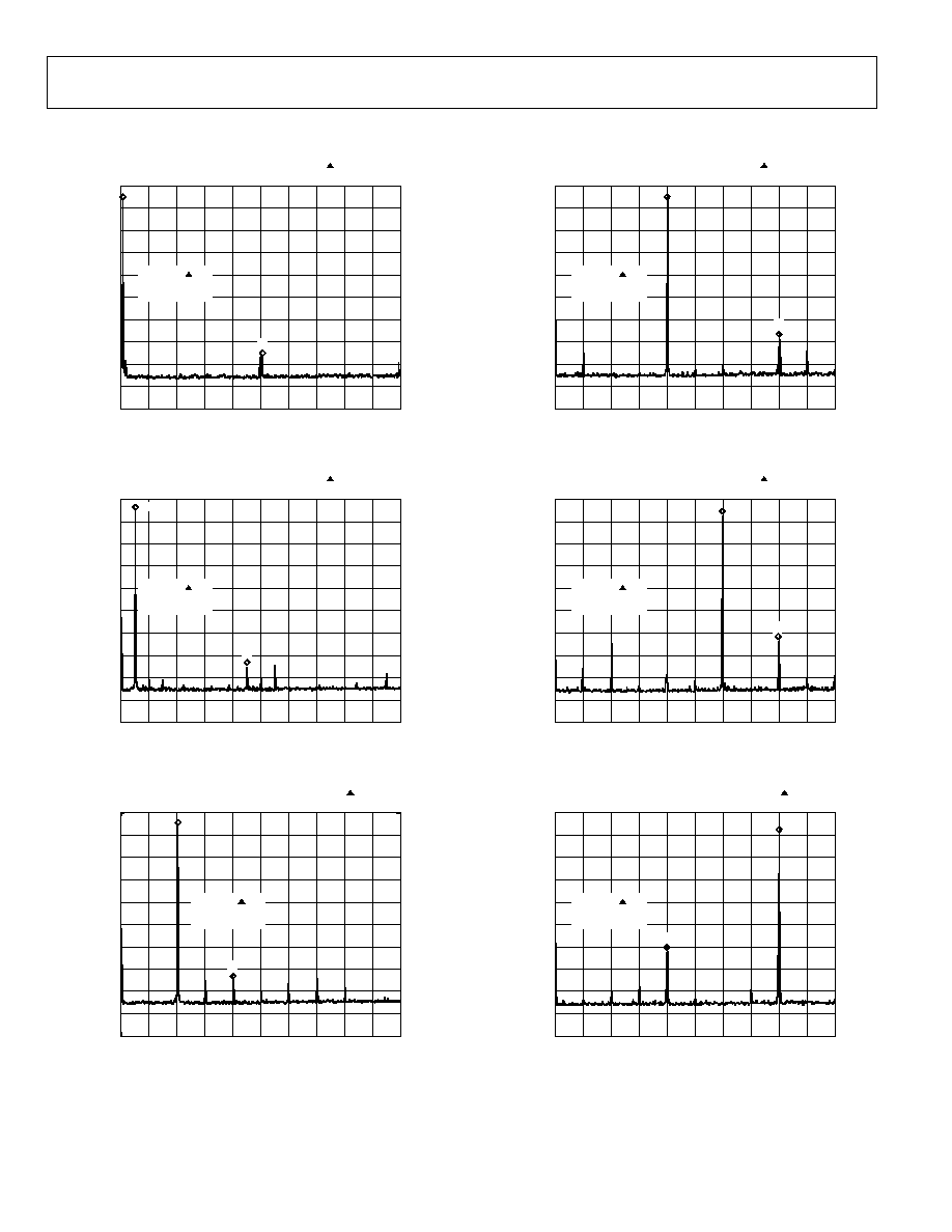
TYPICAL PERFORMANCE CHARACTERISTICS
CENTER 100MHz
#RES BW 3kHz
≠100
≠90
≠80
≠70
≠60
≠50
≠40
≠30
≠20
≠10
0
VBW 3kHz
SPAN 200MHz
SWEEP 55.56 s (401 PTS)
W1 S2
S3 FC
AA
REF 0dBm
PEAK
LOG
10dB/
ATTEN 10dB
MKR1 98.0MHz
≠70.68dB
1
1R
03374-0-016
MARKER
100.000000MHz
≠70.68dB
Figure 4. F
OUT
= 1 MHz FCLK = 400 MSPS, WBSFDR
CENTER 100MHz
#RES BW 3kHz
≠100
≠90
≠80
≠70
≠60
≠50
≠40
≠30
≠20
≠10
0
VBW 3kHz
SPAN 200MHz
SWEEP 55.56 s (401 PTS)
W1 S2
S3 FC
AA
REF 0dBm
PEAK
LOG
10dB/
ATTEN 10dB
MKR1 80.0MHz
≠69.12dB
1
1R
03374-0-017
MARKER
80.000000MHz
≠69.12dB
Figure 5. F
OUT
= 10 MHz, FCLK = 400 MSPS, WBSFDR
CENTER 100MHz
#RES BW 3kHz
≠100
≠90
≠80
≠70
≠60
≠50
≠40
≠30
≠20
≠10
0
VBW 3kHz
SPAN 200MHz
SWEEP 55.56 s (401 PTS)
W1 S2
S3 FC
AA
REF 0dBm
PEAK
LOG
10dB/
ATTEN 10dB
MKR1 0Hz
≠68.44dB
1
1R
03374-0-018
MARKER
40.000000MHz
≠68.44dB
Figure 6. F
OUT
= 40 MHz, FCLK = 400 MSPS, WBSFDR
CENTER 100MHz
#RES BW 3kHz
≠100
≠90
≠80
≠70
≠60
≠50
≠40
≠30
≠20
≠10
0
VBW 3kHz
SPAN 200MHz
SWEEP 55.56 s (401 PTS)
W1 S2
S3 FC
AA
REF 0dBm
PEAK
LOG
10dB/
ATTEN 10dB
MKR1 80.0MHz
≠61.55dB
1
1R
03374-0-019
MARKER
80.000000MHz
≠61.55dB
Figure 7. F
OUT
= 80 MHz FCLK = 400 MSPS, WBSFDR
CENTER 100MHz
#RES BW 3kHz
≠100
≠90
≠80
≠70
≠60
≠50
≠40
≠30
≠20
≠10
0
VBW 3kHz
SPAN 200MHz
SWEEP 55.56 s (401 PTS)
W1 S2
S3 FC
AA
REF 0dBm
PEAK
LOG
10dB/
ATTEN 10dB
MKR1 40.0MHz
≠56.2dB
1
1R
03374-0-020
MARKER
40.000000MHz
≠56.2dB
Figure 8. F
OUT
= 120 MHz, FCLK = 400 MSPS, WBSFDR
CENTER 100MHz
#RES BW 3kHz
≠100
≠90
≠80
≠70
≠60
≠50
≠40
≠30
≠20
≠10
0
VBW 3kHz
SPAN 200MHz
SWEEP 55.56 s (401 PTS)
W1 S2
S3 FC
AA
REF 0dBm
PEAK
LOG
10dB/
ATTEN 10dB
MKR1 0Hz
≠53.17dB
1
1R
03374-0-021
MARKER
80.000000MHz
≠53.17dB
Figure 9. F
OUT
= 160 MHz, FCLK = 400 MSPS, WBSFDR
AD9952
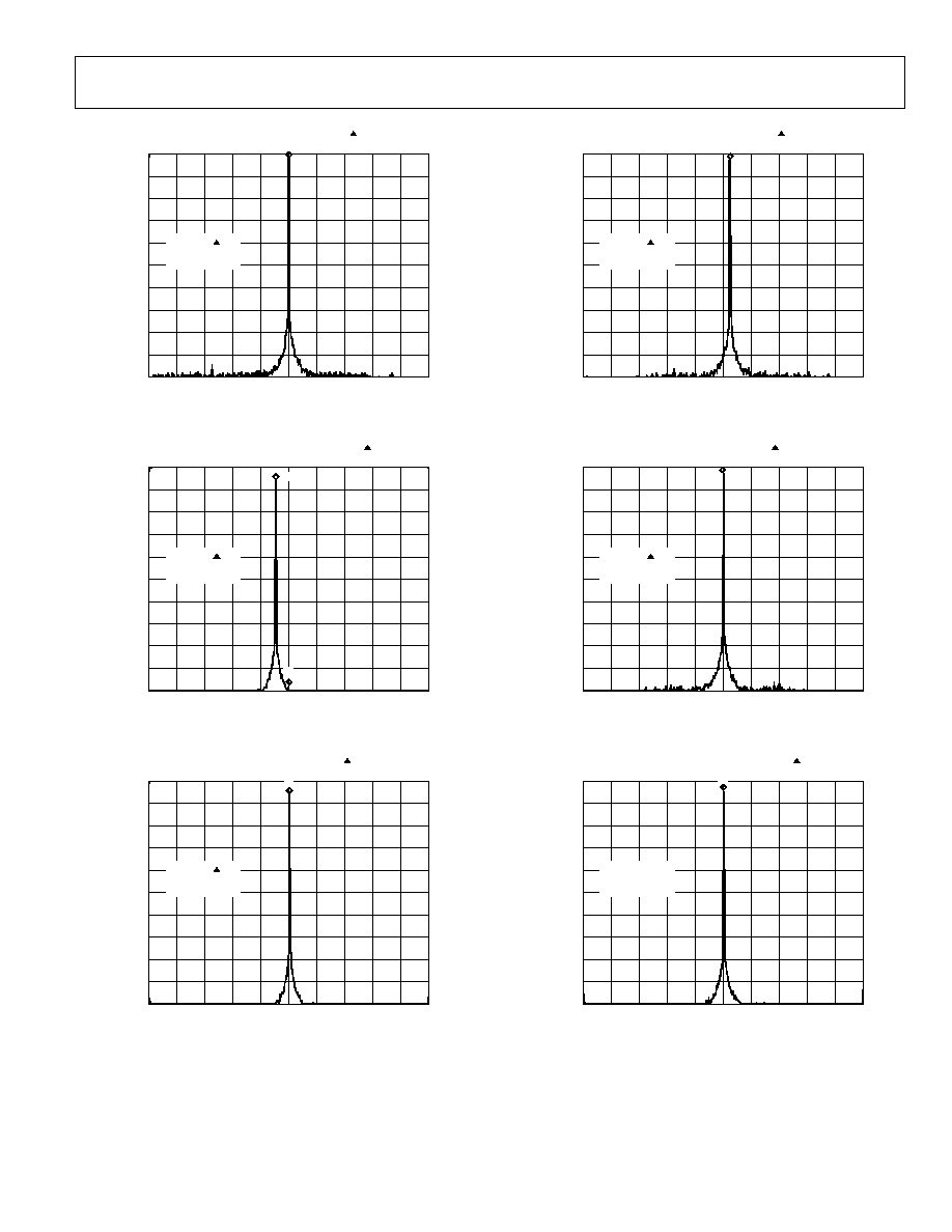
Rev. 0 | Page 11 of 28
CENTER 1.105MHz
#RES BW 30Hz
≠100
≠90
≠80
≠70
≠60
≠50
≠40
≠30
≠20
≠10
0
VBW 30Hz
SPAN 2MHz
SWEEP 199.2 s (401 PTS)
W1 S2
S3 FC
AA
ST
REF ≠4dBm
PEAK
LOG
10dB/
ATTEN 10dB
MKR1 1.105MHz
≠5.679dBm
1
03374-0-022
MARKER
1.105000MHz
≠5.679dBm
Figure 10. F
OUT
= 1.1 MHz, FCLK = 400 MSPS, NBSFDR, ±1 MHz
CENTER 10MHz
#RES BW 30Hz
≠100
≠90
≠80
≠70
≠60
≠50
≠40
≠30
≠20
≠10
0
VBW 30Hz
SPAN 2MHz
SWEEP 199.2 s (401 PTS)
W1 S2
S3 FC
AA
REF 0dBm
PEAK
LOG
10dB/
ATTEN 10dB
MKR1 85kHz
≠93.01dB
1
1R
03374-0-023
MARKER
40.000000MHz
≠56.2dB
Figure 11. F
OUT
= 10 MHz, FCLK = 400 MSPS, NBSFDR, ±1 MHz
CENTER 39.9MHz
#RES BW 30Hz
≠100
≠90
≠80
≠70
≠60
≠50
≠40
≠30
≠20
≠10
0
VBW 30Hz
SPAN 2MHz
SWEEP 199.2 s (401 PTS)
W1 S2
S3 FC
AA
REF 0dBm
PEAK
LOG
10dB/
ATTEN 10dB
MKR1 39.905MHz
≠5.347dBm
1
03374-0-024
MARKER
39.905000MHz
≠5.347dBm
Figure 12. F
OUT
= 39.9 MHz, FCLK = 400 MSPS, NBSFDR, ±1 MHz
CENTER 80.25MHz
#RES BW 30Hz
≠100
≠90
≠80
≠70
≠60
≠50
≠40
≠30
≠20
≠10
0
VBW 30Hz
SPAN 2MHz
SWEEP 199.2 s (401 PTS)
W1 S2
S3 FC
AA
ST
REF ≠4dBm
PEAK
LOG
10dB/
ATTEN 10dB
MKR1 80.301MHz
≠6.318dBm
1
03374-0-025
MARKER
80.301000MHz
≠6.318dBm
Figure 13. F
OUT
= 80.3 MHz, FCLK = 400 MSPS, NBSFDR, ±1 MHz
CENTER 120.2MHz
#RES BW 30Hz
≠100
≠90
≠80
≠70
≠60
≠50
≠40
≠30
≠20
≠10
0
VBW 30Hz
SPAN 2MHz
SWEEP 199.2 s (401 PTS)
W1 S2
S3 FC
AA
ST
REF ≠4dBm
PEAK
LOG
10dB/
ATTEN 10dB
MKR1 120.205MHz
≠6.825dBm
1
03374-0-026
MARKER
120.205000MHz
≠6.825dBm
Figure 14. F
OUT
= 120.2 MHz, FCLK = 400 MSPS, NBSFDR, ±1 MHz
CENTER 160.5MHz
#RES BW 30Hz
≠100
≠90
≠80
≠70
≠60
≠50
≠40
≠30
≠20
≠10
0
VBW 30Hz
SPAN 2MHz
SWEEP 199.2 s (401 PTS)
W1 S2
S3 FC
AA
ST
REF ≠4dBm
PEAK
LOG
10dB/
ATTEN 10dB
MKR1 600kHz
≠0.911dB
1
03374-0-027
CENTER
160.5000000MHz
Figure 15. F
OUT
= 160 MHz, FCLK = 400 MSPS, NBSFDR, ±1 MHz
AD9952
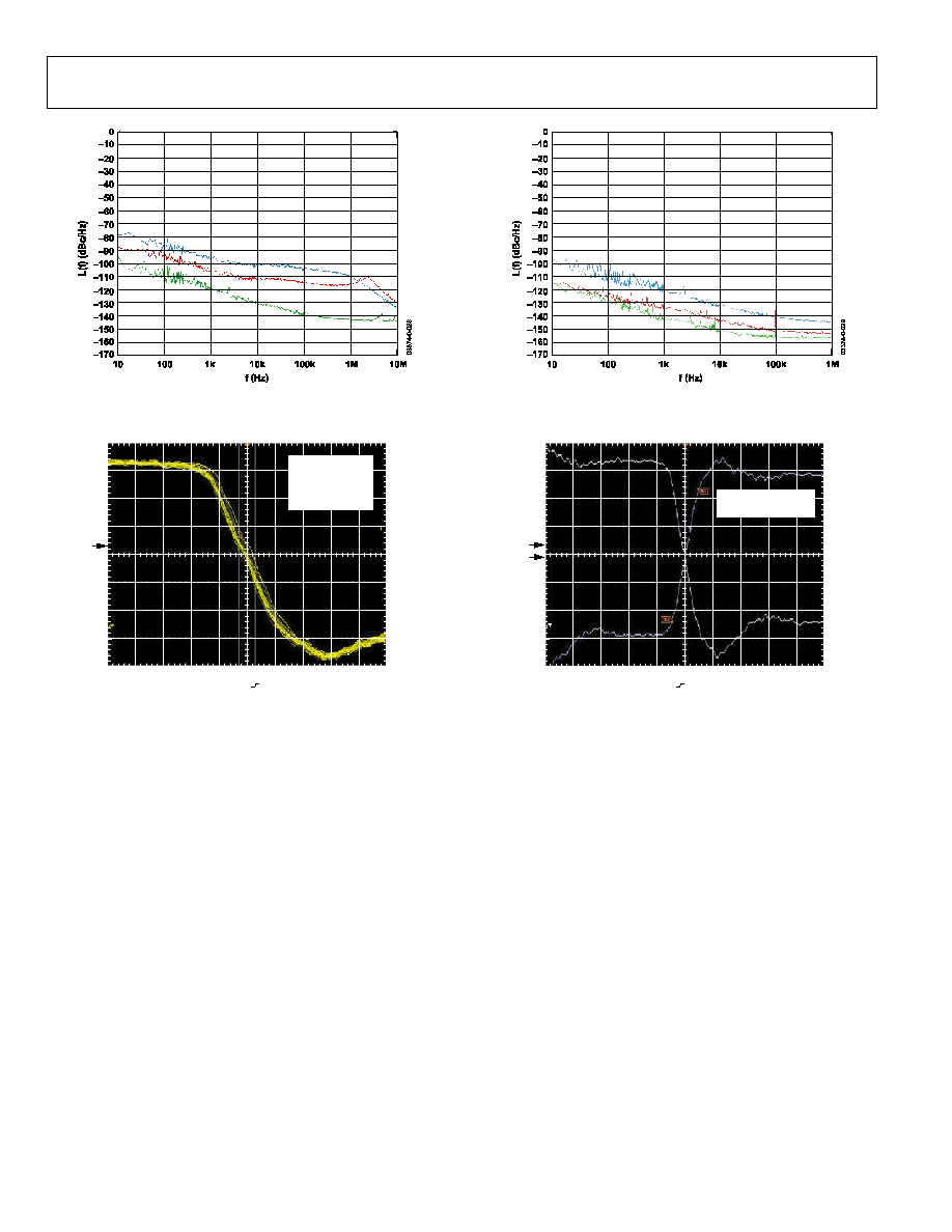
Rev. 0 | Page 12 of 28
Figure 16. Residual Phase Noise with F
OUT
= 159.5 MHz, F
CLK
= 400 MSPS
(Green), 4 ◊ 100 MSPS (Red), and 20 ◊ 20 MSPS (Blue)
CH1 200mV
1
IT 4.0PS/PT 3.1ns
M 200PS 20.0GS/S
A CH1 708mV
03374-0-031
t
1 = 3.156ns
t
2 = 3.04ns
t =
≠116.0PS
1/
t =
≠8.621GHz
Figure 17. Residual Peak-to-Peak Jitter of DDS
and Comparator Operating Together at 160 MHz
Figure 18. Residual Phase Noise with F
OUT
= 9.5 MHz, F
CLK
= 400 MSPS (Green),
4 ◊100 MSPS (Red), and 20 ◊ 20 MSPS (Blue)
REF2 200mV 500ns
R2
R1
IT 10.0PS/PT ≠100PS
M 500PS 20.0GS/S
A CH1 708mV
03374-0-030
FALL (R1) = 396.4PS
RISE(R2) = 464.3PS
Figure 19. Comparator Rise and Fall Time at 160 MHz

AD9952
Rev. 0 | Page 13 of 28
THEORY OF OPERATION
COMPONENT BLOCKS
DDS Core
The output frequency (f
O
) of the DDS is a function of the
frequency of the system clock (SYSCLK), the value of the
frequency tuning word (FTW), and the capacity of the
accumulator (2
32
, in this case). The exact relationship is given
below with f
S
defined as the frequency of SYSCLK.
(
)
( )
31
32
2
0
2
/
=
FTW
with
f
FTW
f
S
O
(
)
(
)
1
≠
2
2
2
/
≠
1
32
31
32
<
<
◊
=
FTW
with
FTW
f
f
S
O
The value at the output of the phase accumulator is translated to
an amplitude value via the COS(x) functional block and routed
to the DAC.
In certain applications, it is desirable to force the output signal
to zero phase. Simply setting the FTW to 0 does not accomplish
this; it only results in the DDS core holding its current phase
value. Thus, a control bit is required to force the phase accumu-
lator output to zero.
At power-up, the clear phase accumulator bit is set to Logic 1,
but the buffer memory for this bit is cleared (Logic 0). There-
fore, upon power-up, the phase accumulator will remain clear
until the first I/O UPDATE is issued.
Phase-Locked Loop (PLL)
The PLL allows multiplication of the REFCLK frequency. Con-
trol of the PLL is accomplished by programming the 5-bit
REFCLK multiplier portion of Control Function Register No. 2,
Bits <7:3>.
When programmed for values ranging from 0x04 to 0x14
(4 decimal to 20 decimal), the PLL multiplies the REFCLK input
frequency by the corresponding decimal value. However, the
maximum output frequency of the PLL is restricted to
400 MHz. Whenever the PLL value is changed, the user should
be aware that time must be allocated to allow the PLL to lock
(approximately 1 ms).
The PLL is bypassed by programming a value outside the range
of 4 to 20 (decimal). When bypassed, the PLL is shut down to
conserve power.
Clock Input
The AD9952 supports various clock methodologies. Support for
differential or single-ended input clocks and enabling of an
on-chip oscillator and/or a phase-locked loop (PLL) multiplier
is all controlled via user programmable bits. The AD9952 may
be configured in one of six operating modes to generate the
system clock. The modes are configured using the CLKMODE-
SELECT pin, CFR1<4>, and CFR2<7:3>. Connecting the exter-
nal pin CLKMODESELECT to Logic High enables the on-chip
crystal oscillator circuit. With the on-chip oscillator enabled,
users of the AD9952 connect an external crystal to the REFCLK
and REFCLKB inputs to produce a low frequency reference
clock in the range of 20 MHz to 30 MHz. The signal generated
by the oscillator is buffered before it is delivered to the rest of
the chip. This buffered signal is available via the CRYSTAL
OUT pin. Bit CFR1<4> can be used to enable or disable the
buffer, turning on or off the system clock. The oscillator itself is
not powered down in order to avoid long start-up times associ-
ated with turning on a crystal oscillator. Writing CFR2<9> to
Logic High enables the crystal oscillator output buffer. Logic
Low at CFR2<9> disables the oscillator output buffer.
Connecting CLKMODESELECT to Logic Low disables the
on-chip oscillator and the oscillator output buffer. With the
oscillator disabled, an external oscillator must provide the
REFCLK and/or REFCLKB signals. For differential operation,
these pins are driven with complementary signals. For single-
ended operation, a 0.1 µF capacitor should be connected
between the unused pin and the analog power supply. With the
capacitor in place, the clock input pin bias voltage is 1.35 V. In
addition, the PLL may be used to multiply the reference
frequency by an integer value in the range of 4 to 20. Table 4
summarizes the clock modes of operation. Note that the PLL
multiplier is controlled via the CFR2<7:3> bits, independent of
the CFR1<4> bit.
Table 4.Clock Input Modes of Operation
CFR1<4> CLKMODESELECT CFR2<7:3>
Oscillator
Enabled?
System Clock
Frequency Range (MHz)
Low
High
3 < M < 21
Yes
F
CLK
= F
OSC
◊ M
80 < F
CLK
< 400
Low
High
M < 4 or M > 20
Yes
F
CLK
= F
OSC
20 < F
CLK
< 30
Low
Low
3 < M < 21
No
F
CLK
= F
OSC
◊ M
80 < F
CLK
< 400
Low
Low
M < 4 or M > 20
No
F
CLK
= F
OSC
10 < F
CLK
< 400
High X
X
No
F
CLK
= 0
N/A

AD9952
Rev. 0 | Page 14 of 28
DAC Output
The AD9952 incorporates an integrated 14-bit current output
DAC. Unlike most DACs, this output is referenced to AVDD,
not AGND.
Two complementary outputs provide a combined full-scale
output current (I
OUT
). Differential outputs reduce the amount of
common-mode noise that might be present at the DAC output,
offering the advantage of an increased signal-to-noise ratio. The
full-scale current is controlled by an external resistor (R
SET
)
connected between the DAC_R
SET
pin and the DAC ground
(AGND_DAC). The full-scale current is proportional to the
resistor value as follows:
OUT
SET
I
R
/
19
.
39
=
The maximum full-scale output current of the combined DAC
outputs is 15 mA, but limiting the output to 10 mA provides the
best spurious-free dynamic range (SFDR) performance. The DAC
output compliance range is AVDD + 0.5 V to AVDD ≠ 0.5 V.
Voltages developed beyond this range will cause excessive DAC
distortion and could potentially damage the DAC output circuitry.
Proper attention should be paid to the load termination to keep the
output voltage within this compliance range.
Comparator
Many applications require a square wave signal rather than a
sine wave. For example, in most clocking applications a high
slew rate helps to reduce phase noise and jitter. To support these
applications, the AD9952 includes an on-chip comparator. The
comparator has a bandwidth greater than 200 MHz and a
common-mode input range of 1.3 V to 1.8 V. By setting the
comparator power-down bit, CFR1<6>, the comparator can be
turned off to save on power consumption.
Serial IO Port
The AD9952 serial port is a flexible, synchronous serial communi-
cations port that allows easy interface to many industry-standard
microcontrollers and microprocessors. The serial I/O port is com-
patible with most synchronous transfer formats, including both the
Motorola 6905/11 SPIÆ and IntelÆ 8051 SSR protocols.
The interface allows read/write access to all registers that configure
the AD9952. MSB first or LSB first transfer formats are supported.
The AD9952's serial interface port can be configured as a single pin
I/O (SDIO), which allows a 2-wire interface or two unidirectional
pins for in/out (SDIO/SDO), which in turn enables a 3-wire inter-
face. Two optional pins, IOSYNC and CS, enable greater flexibility
for system design in the AD9952.
Register Map and Descriptions
The register map is listed in Table 5.
AD9952
Rev. 0 | Page 15 of 28
Table 5. Register Map
Register
Name
(Serial
Address)
Bit
Range
(MSB)
Bit 7
Bit 6
Bit 5
Bit 4
Bit 3
Bit 2
Bit 1
(LSB)
Bit 0
Default
Value
<7:0>
Digital
Power-
Down
Comparator
Power-
Down
DAC
Power-
Down
Clock Input
Power-
Down
External
Power-
Down
Mode
Not Used
SYNC_CLK
Out
Disable
Not
Used
0x00
<15:8>
Not Used
Not Used
AutoClr
Phase
Accum.
Enable SINE
Output
Not
Used
Clear
Phase
Accum.
SDIO
Input
Only
LSB First
0x00
<23:16>
Automatic
Sync
Enable
Software
Manual
Sync
Not Used
0x00
Control
Function
Register
No.1
(CFR1)
(0x00)
<31:24> Not
Used
Load ARR
@ I/O UD
OSK
Enable
Auto
OSK
Keying
0x00
<7:0>
REFCLK Multiplier
0x00 or 0x01, or 0x02 or 0x03: Bypass Multiplier
0x04 to 0x14: 4◊ to 20◊ Multiplication
VCO
Range
Charge Pump Current
<1:0>
0x00
<15:8> Not
Used
High
Speed
Sync
Enable
Hardware
Manual
Sync
Enable
CRYSTAL
OUT Pin
Active
Not
Used
0x00
Control
Function
Register
No. 2
(CFR2)
(0x01)
<23:16> Not
Used 0x00
<7:0>
Amplitude Scale Factor Register <7:0>
0x00
Amplitude
Scale
Factor
(ASF)
(0x02)
<15:8>
Auto Ramp Rate Speed
Control <1:0>
Amplitude Scale Factor Register <13:8>
0x00
Amplitude
Ramp Rate
(ARR)
(0x03)
<7:0>
Amplitude Ramp Rate Register <7:0>
0x00
<7:0>
Frequency Tuning Word No. 0 <7:0>
0x00
<15:8>
Frequency Tuning Word No. 0 <15:8>
0x00
<23:16>
Frequency Tuning Word No. 0 <23:16>
0x00
Frequency
Tuning
Word
(FTW0)
(0x04)
<31:24>
Frequency Tuning Word No. 0 <31:24>
0x00
<7:0>
Phase Offset Word No. 0 <7:0>
0x00
Phase
Offset
Word
(POW0)
(0x05)
<15:8> Not
Used<1:0>
Phase
Offset Word No. 0 <13:8>
0x00

AD9952
Rev. 0 | Page 16 of 28
Control Register Bit Descriptions
Control Function Register No. 1 (CFR1)
The CFR1 is used to control the various functions, features,
and modes of the AD9952. The functionality of each bit is
detailed below.
CFR1<31:27>: Not Used
CFR1<26>: Amplitude Ramp Rate Load Control Bit
CFR1<26> = 0 (default). The amplitude ramp rate timer is
loaded only upon timeout (timer == 1) and is not loaded due to
an I/O UPDATE input signal.
CFR1<26> = 1. The amplitude ramp rate timer is loaded upon
timeout (timer == 1) or at the time of an I/O UPDATE input signal.
CFR1<25>: Shaped On-Off Keying Enable Bit
CFR1<25> = 0 (default). Shaped on-off keying is bypassed.
CFR1<25> = 1. Shaped on-off keying is enabled. When enabled,
CFR1<24> controls the mode of operation for this function.
CFR1<24>: Auto Shaped On-Off Keying Enable Bit (Only Valid
when CFR1<25> Is Active High)
CFR1<24> = 0 (default). When CFR1<25> is active, a Logic 0
on CFR1<24> enables the manual shaped on-off keying opera-
tion. Each amplitude sample sent to the DAC is multiplied by
the amplitude scale factor. See the Shaped On-Off Keying sec-
tion for details.
CFR1<24> = 1. When CFR1<25> is active, a Logic 1 on
CFR1<24> enables the auto shaped on-off keying operation.
Toggling the OSK pin high will cause the output scalar to ramp
up from zero scale to the amplitude scale factor at a rate deter-
mined by the amplitude ramp rate. Toggling the OSK pin low
will cause the output to ramp down from the amplitude scale
factor to zero scale at the amplitude ramp rate. See the Shaped
On-Off Keying section for details.
CFR1<23>: Automatic Synchronization Enable Bit
CFR1<23> = 0 (default). The automatic synchronization feature
of multiple AD9952s is inactive.
CFR1<23> = 1. The automatic synchronization feature of mul-
tiple AD9952s is active. The device will synchronize its internal
synchronization clock (SYNC_CLK) to align to the signal pre-
sent on the SYNC_IN input. See the Synchronizing Multiple
AD9952s section for details.
CFR1<22>: Software Manual Synchronization of Multiple
AD9952s.
CFR1<22> = 0 (default). The manual synchronization feature is
inactive.
CFR1<22> = 1. The software controlled manual synchroniza-
tion feature is executed. The SYNC_CLK rising edge is
advanced by one SYNC_CLK cycle and this bit is cleared. To
advance the rising edge multiple times, this bit needs to be set
for each advance. See the Synchronizing Multiple AD9952s sec-
tion for details.
CFR1<21:14>: Not Used
CFR1<13>: Auto-Clear Phase Accumulator Bit
CFR1<13> = 0 (default). The current state of the phase accumu-
lator remains unchanged when the frequency tuning word is
applied.
CFR1<13> = 1. This bit automatically synchronously clears
(loads 0s into) the phase accumulator for one cycle upon recep-
tion of an I/O UPDATE signal.
CFR1<12>: Sine/Cosine Select Bit
CFR1<12> = 0 (default). The angle-to-amplitude conversion
logic employs a COSINE function.
CFR1<12> = 1. The angle-to-amplitude conversion logic
employs a SINE function.
CFR1<11>: Not Used
CFR1<10>: Clear Phase Accumulator
CFR1<10> = 0 (default). The phase accumulator functions as
normal.
CFR1<10> = 1. The phase accumulator memory elements are
cleared and held clear until this bit is cleared.
CFR1<9>: SDIO Input Only
CFR1<9> = 0 (default). The SDIO pin has bidirectional opera-
tion (2-wire serial programming mode).
CFR1<9> = 1. The serial data I/O pin (SDIO) is configured as
an input only pin (3-wire serial programming mode).
CFR1<8>: LSB First
CFR1<8> = 0 (default). MSB first format is active.
CFR1<8> = 1. The serial interface accepts serial data in LSB first
format.
CFR1<7>: Digital Power-Down Bit
CFR1<7> = 0 (default). All digital functions and clocks are active.
CFR1<7> = 1. All non-IO digital functionality is suspended,
lowering the power significantly.

AD9952
Rev. 0 | Page 17 of 28
CFR1<6>: Comparator Power-Down Bit
CFR1<6> = 0 (default). The comparator is enabled for operation.
CFR1<6> = 1. The comparator is disabled and is in its lowest
power dissipation state.
CFR1<5>: DAC Power-Down Bit
CFR1<5> = 0 (default). The DAC is enabled for operation.
CFR1<5> = 1. The DAC is disabled and is in its lowest power
dissipation state.
CFR1<4>: Clock Input Power-Down Bit
CFR1<4> = 0 (default). The clock input circuitry is enabled for
operation.
CFR1<4> = 1. The clock input circuitry is disabled and the
device is in its lowest power dissipation state.
CFR1<3>: External Power-Down Mode
CFR1<3> = 0 (default). The external power-down mode
selected is the rapid recovery power-down mode. In this mode,
when the PWRDWNCTL input pin is high, the digital logic
and the DAC digital logic are powered down. The DAC bias
circuitry, PLL, oscillator, and clock input circuitry are not
powered down.
CFR1<3> = 1. The external power-down mode selected is the
full power-down mode. In this mode, when the PWRDWNCTL
input pin is high, all functions are powered down. This includes
the DAC and PLL, which take a significant amount of time to
power up.
CFR1<2>: Not Used
CFR1<1>: SYNC_CLK Disable Bit
CFR1<1> = 0 (default). The SYNC_CLK pin is active.
CFR1<1> = 1. The SYNC_CLK pin assumes a static Logic 0
state to keep noise generated by the digital circuitry at a mini-
mum. However, the synchronization circuitry remains active
(internally) to maintain normal device timing.
CFR1<0>: Not Used, Leave at 0
Control Function Register No. 2 (CFR2)
The CFR2 is used to control the various functions, features, and
modes of the AD9952, primarily related to the analog sections
of the chip.
CFR2<23:12>: Not Used
CFR2<11>: High Speed Sync Enable Bit
CFR2<11> = 0 (default). The high speed sync enhancement is off.
CFR2<11> = 1. The high speed sync enhancement is on. This
bit should be set when attempting to use the auto-
synchronization feature for SYNC_CLK inputs beyond 50 MHz,
(200 MSPS SYSCLK). See the Synchronizing Multiple AD9952s
section for details.
CFR2<10>: Hardware Manual Sync Enable Bit
CFR2<10> = 0 (default). The hardware manual sync function is off.
CFR2<10> = 1. The hardware manual sync function is enabled.
While this bit is set, a rising edge on the SYNC_IN pin will
cause the device to advance the SYNC_CLK rising edge by one
REFCLK cycle. Unlike the software manual sync enable bit, this
bit does not self-clear. Once the hardware manual sync mode is
enabled, it will stay enabled until this bit is cleared. See the
Synchronizing Multiple AD9952s section for details.
CFR2<9>: CRYSTAL OUT Enable Bit
CFR2<9> = 0 (default). The CRYSTAL OUT pin is inactive.
CFR2<9> = 1. The CRYSTAL OUT pin is active. When active,
the crystal oscillator circuitry output drives the CRYSTAL OUT
pin, which can be connected to other devices to produce a refer-
ence frequency. The oscillator will respond to crystals in the
range of 20 MHz to 30 MHz.
CFR2<8>: Not Used
CFR2<7:3>: Reference Clock Multiplier Control Bits
This 5-bit word controls the multiplier value out of the clock-
multiplier (PLL) block. Valid values are decimal 4 to 20 (0x04 to
0x14). Values entered outside this range will bypass the clock
multiplier. See the Phase-Locked Loop (PLL) section for details.
CFR2<2>: VCO Range Control Bit
This bit is used to control the range setting on the VCO.
When CFR2<2> == 0 (default), the VCO operates in a range of
100 MHz to 250 MHz. When CFR2<2> == 1, the VCO operates
in a range of 250 MHz to 400 MHz.
CFR2<1:0>: Charge Pump Current Control Bits
These bits are used to control the current setting on the charge
pump. The default setting, CFR2<1:0>, sets the charge pump
current to the default value of 75 µA. For each bit added (01, 10,
11), 25 µA of current is added to the charge pump current:
100 µA, 125 µA, and 150 µA.

AD9952
Rev. 0 | Page 18 of 28
Other Register Descriptions
Amplitude Scale Factor (ASF)
The ASF register stores the 2-bit auto ramp rate speed value
and the 14-bit amplitude scale factor used in the output shaped
keying (OSK) operation. In auto OSK operation, ASF <15:14>
tells the OSK block how many amplitude steps to take for each
increment or decrement. ASF<13:0> sets the maximum value
achievable by the OSK internal multiplier. In manual OSK
mode, ASF<15:14> has no effect. ASF <13:0> provides the
output scale factor directly. If the OSK enable bit is cleared,
CFR1<25> = 0, this register has no effect on device operation.
Amplitude Ramp Rate (ARR)
The ARR register stores the 8-bit amplitude ramp rate used in
the auto OSK mode. This register programs the rate at which
the amplitude scale factor counter increments or decrements. If
the OSK is set to manual mode, or if OSK enable is cleared, this
register has no effect on device operation.
Frequency Tuning Word 0 (FTW0)
The frequency tuning word is a 32-bit register that controls the
rate of accumulation in the phase accumulator of the DDS core.
Its specific role is dependent on the device mode of operation.
Phase Offset Word (POW)
The phase offset word is a 14-bit register that stores a phase
offset value. This offset value is added to the output of the phase
accumulator to offset the current phase of the output signal. The
exact value of phase offset is given by the following formula:
∞
◊
=
360
2
14
POW
MODES OF OPERATION
Single-Tone Mode
In single-tone mode, the DDS core uses a single tuning word.
Whatever value is stored in FTW0 is supplied to the phase
accumulator. This value can only be changed manually, which is
done by writing a new value to FTW0 and by issuing an I/O
UPDATE. Phase adjustment is possible through the phase
offset register.
PROGRAMMING AD9952 FEATURES
Phase Offset Control
A 14-bit phase offset () may be added to the output of the phase
accumulator by means of the control registers. This feature provides
the user with two different methods of phase control.
The first method is a static phase adjustment, where a fixed
phase offset is loaded into the appropriate phase offset register
and left unchanged. The result is that the output signal is offset
by a constant angle relative to the nominal signal. This allows
the user to phase align the DDS output with some external
signal, if necessary.
The second method of phase control is where the user regularly
updates the phase offset register via the I/O port. By properly
modifying the phase offset as a function of time, the user can
implement a phase modulated output signal. However, both the
speed of the I/O port and the frequency of SYSCLK limit the
rate at which phase modulation can be performed.
The AD9952 allows for a programmable continuous zeroing of
the phase accumulator as well as a clear and release or auto-
matic zeroing function. Each feature is individually controlled
via the CFR1 bits. CFR1<13> is the automatic clear phase ac-
cumulator bit. CFR1<10> clears the phase accumulator and
holds the value to zero.
Continuous Clear Bit
The continuous clear bit is simply a static control signal that,
when active high, holds the phase accumulator at zero for the
entire time the bit is active. When the bit goes low, inactive, the
phase accumulator is allowed to operate.
Clear and Release Function
When set, the auto-clear phase accumulator clears and releases
the phase accumulator upon receiving an I/O UPDATE. The
automatic clearing function is repeated for every subsequent
I/O UPDATE until the appropriate auto-clear control bit is
cleared.
Shaped On-Off Keying
The shaped on-off keying function of the AD9952 allows the
user to control the ramp-up and ramp-down time of an on-off
emission from the DAC. This function is used in burst trans-
missions of digital data to reduce the adverse spectral impact of
short, abrupt bursts of data.
Auto and manual shaped on-off keying modes are supported.
The auto mode generates a linear scale factor at a rate deter-
mined by the amplitude ramp rate (ARR) register controlled by
an external pin (OSK). Manual mode allows the user to directly
control the output amplitude by writing the scale factor value
into the amplitude scale factor (ASF) register.
The shaped on-off keying function may be bypassed (disabled)
by clearing the OSK enable bit (CFR1<25> = 0).
The modes are controlled by two bits located in the most sig-
nificant byte of the control function register (CFR). CFR1<25>
is the shaped on-off keying enable bit. When CFR1<25> is set,
the output scaling function is enabled and CFR1<25> bypasses
the function. CFR1<24> is the internal shaped on-off keying
active bit. When CFR1<24> is set, internal shaped on-off keying
mode is active; CFR1<24> is cleared, external shaped on-off
keying mode is active. CFR1<24> is a Don't Care if the shaped
on-off keying enable bit (CFR1<25>) is cleared. The power up
condition is shaped on-off keying disabled (CFR1<25> = 0).
Figure 20 shows the block diagram of the OSK circuitry.
AD9952
Rev. 0 | Page 19 of 28
AUTO Shaped On-Off Keying Mode Operation
The auto shaped on-off keying mode is active when CFR1<25>
and CFR1<24> are set. When auto shaped on-off keying mode
is enabled, a single-scale factor is internally generated and
applied to the multiplier input for scaling the output of the DDS
core block (see Figure 20). The scale factor is the output of a
14-bit counter that increments/decrements at a rate determined
by the contents of the 8-bit output ramp rate register. The scale
factor increases if the OSK pin is high and decreases if the OSK
pin is low. The scale factor is an unsigned value such that all 0s
multiply the DDS core output by 0 (decimal) and 0x3FFF mul-
tiplies the DDS core output by 16383 (decimal).
For those users who use the full amplitude (14-bits) but need
fast ramp rates, the internally generated scale factor step size
is controlled via the ASF<15:14> bits. Table 6 describes the
increment/decrement step size of the internally generated scale
factor per the ASF<15:14> bits.
A special feature of this mode is that the maximum output
amplitude allowed is limited by the contents of the amplitude
scale factor register. This allows the user to ramp to a value less
than full scale.
Table 6. Auto-Scale Factor Internal Step Size
ASF<15:14> (Binary)
Increment/Decrement Size
00 1
01 2
10 4
11 8
OSK Ramp Rate Timer
The OSK ramp rate timer is a loadable down counter, which
generates the clock signal to the 14-bit counter that generates
the internal scale factor. The ramp rate timer is loaded with the
value of the ASFR every time the counter reaches 1 (decimal).
This load and countdown operation continues for as long as the
timer is enabled, unless the timer is forced to load before reach-
ing a count of 1.
If the load OSK timer bit (CFR1<26>) is set, the ramp rate timer
is loaded upon an I/O UPDATE or upon reaching a value of 1.
The ramp timer can be loaded before reaching a count of 1 by
three methods.
The first method of loading is by changing the OSK input pin.
When the OSK input pin changes state, the ASFR value is
loaded into the ramp rate timer, which then proceeds to count
down as normal.
The second method in which the sweep ramp rate timer can be
loaded before reaching a count of 1 is if the load OSK timer bit
(CFR1<26>) is set and an I/O UPDATE is issued.
The last method in which the sweep ramp rate timer can be
loaded before reaching a count of 1 is when going from the
inactive auto shaped on-off keying mode to the active auto
shaped on-off keying mode; that is, when the sweep enable bit is
being set.
03374-0-005
OSK PIN
LOAD OSK TIMER
CFR1<26>
SYNC_CLK
AUTO DESK
ENABLE
CFR1<24>
TO DAC
AUTO SCALE
FACTOR GENERATOR
RAMP RATE TIMER
CLOCK
DDS CORE
OSK ENABLE
CFR<25>
AMPLITUDE SCALE
FACTOR REGISTER
(ASF)
0
0
1
01
0
1
HOLD
INC/DEC ENABLE
OUT
COS(X)
AMPLITUDE RAMP
RATE REGISTER
(ASF)
UP/DN
DATA
LOAD
EN
Figure 20. On-Off Shaped Keying, Block Diagram
AD9952
Rev. 0 | Page 20 of 28
External Shaped On-Off Keying Mode Operation
The external shaped on-off keying mode is enabled by writing
CFR1<25> to a Logic 1 and writing CFR1<24> to a Logic 0.
When configured for external shaped on-off keying, the
content of the ASFR becomes the scale factor for the data path.
The scale factors are synchronized to SYNC_CLK via the
I/O UPDATE functionality.
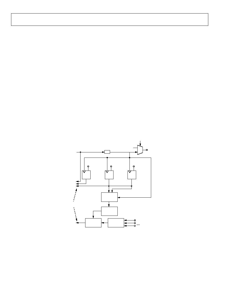
Synchronization; Register Updates (I/O UPDATE)
Functionality of the SYNC_CLK and I/O UPDATE
Data into the AD9952 is synchronous to the SYNC_CLK signal
(supplied externally to the user on the SYNC_CLK pin). The
I/O UPDATE pin is sampled on the rising edge of the
SYNC_CLK.
Internally, SYSCLK is fed to a divide-by-4 frequency divider to
produce the SYNC_CLK signal. The SYNC_CLK signal is pro-
vided to the user on the SYNC_CLK pin. This enables synchro-
nization of external hardware with the device's internal clocks.
This is accomplished by forcing any external hardware to obtain
its timing from SYNC_CLK. The I/O UPDATE signal coupled
with SYNC_CLK is used to transfer internal buffer contents
into the control registers of the device. The combination of the
SYNC_CLK and I/O UPDATE pins provides the user with
constant latency relative to SYSCLK, and also ensures phase
continuity of the analog output signal when a new tuning word
or phase offset value is asserted. Figure 21 demonstrates an I/O
UPDATE timing cycle and synchronization.
Notes to synchronization logic:
1)
The I/O UPDATE signal is edge detected to generate a
single rising edge clock signal that drives the register bank
flops. The I/O UPDATE signal has no constraints on duty
cycle. The minimum low time on I/O UPDATE is one
SYNC_CLK clock cycle.
2)
The I/O UPDATE pin is set up and held around the rising
edge of SYNC_CLK and has zero hold time and 4 ns setup
time.
03374-0-006
SYSCLK
SDI
SYNC_CLK
DISABLE
10
0
SCLK
TO CORE LOGIC
CS
OSK
D
Q
PROFILE<1:0>
D
Q
I/O UPDATE
D
Q
˜ 4
SYNC_CLK
GATING
EDGE
DETECTION
LOGIC
REGISTER
MEMORY
I/O BUFFER
LATCHES
Figure 21. I/O Synchronization Block Diagram
AD9952
Rev. 0 | Page 21 of 28
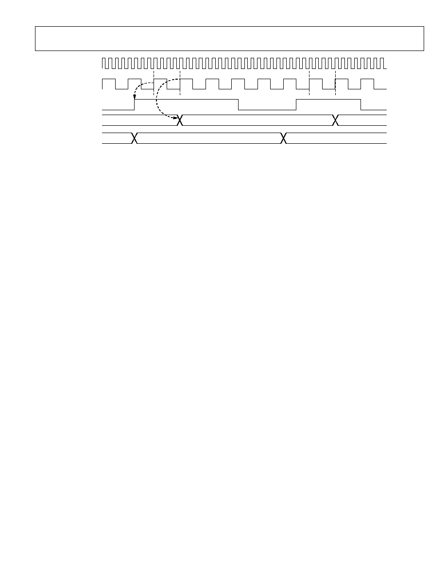
SYNC_CLK
SYSCLK
A
B
DATA 2
DATA 3
DATA 1
DATA IN
REGISTERS
DATA IN
I/O BUFFERS
DATA 1
DATA 2
DATA 3
I/O UPDATE
THE DEVICE REGISTERS AN I/O UPDATE AT POINT A. THE DATA IS TRANSFERRED FROM THE ASYNCHRONOUSLY LOADED I/O BUFFERS AT POINT B.
03374-0-007
Figure 22. I/O Synchronization Timing Diagram
Synchronizing Multiple AD9952s
The AD9952 product allows easy synchronization of multiple
AD9952s. There are three modes of synchronization available
to the user: an automatic synchronization mode, a software
controlled manual synchronization mode, and a hardware
controlled manual synchronization mode. In all cases, when a
user wants to synchronize two or more devices, the following
considerations must be observed. First, all units must share a
common clock source. Trace lengths and path impedance of the
clock tree must be designed to keep the phase delay of the dif-
ferent clock branches as closely matched as possible. Second, the
I/O UPDATE signal's rising edge must be provided synchro-
nously to all devices in the system. Finally, regardless of the
internal synchronization method used, the DVDD_I/O supply
should be set to 3.3 V for all devices that are to be synchronized.
AVDD and DVDD should be left at 1.8 V.
In automatic synchronization mode, one device is chosen as a
master; the other device(s) will be slaved to this master. When
configured in this mode, the slaves will automatically synchro-
nize their internal clocks to the SYNC_CLK output signal of the
master device. To enter automatic synchronization mode, set the
slave device's automatic synchronization bit (CFR1<23> = 1).
Connect the SYNC_IN input(s) to the master SYNC_CLK
output. The slave device will continuously update the phase
relationship of its SYNC_CLK until it is in phase with the
SYNC_IN input, which is the SYNC_CLK of the master device.
When attempting to synchronize devices running at SYSCLK
speeds beyond 250 MSPS, the high speed sync enhancement
enable bit should be set (CFR2<11> = 1).
In software manual synchronization mode, the user forces the
device to advance the SYNC_CLK rising edge one SYSCLK
cycle (1/4 SYNC_CLK period). To activate the manual synchro-
nization mode, set the slave device's software manual synchroni-
zation bit (CFR1<22> = 1). The bit (CFR1<22>) will be cleared
immediately. To advance the rising edge of the SYNC_CLK multi-
ple times, this bit will need to be set multiple times.
In hardware manual synchronization mode, the SYNC_IN
input pin is configured such that it will now advance the rising
edge of the SYNC_CLK signal each time the device detects a
rising edge on the SYNC_IN pin. To put the device into hard-
ware manual synchronization mode, set the hardware manual
synchronization bit (CFR2<10> = 1). Unlike the software man-
ual synchronization bit, this bit does not self-clear. Once the
hardware manual synchronization mode is enabled, all rising
edges detected on the SYNC_IN input will cause the device to
advance the rising edge of the SYNC_CLK by one SYSCLK
cycle until this enable bit is cleared (CFR2<10> = 0).
Using a Single Crystal to Drive Multiple AD9952 Clock
Inputs
The AD9952 crystal oscillator output signal is available on the
CRYSTAL OUT pin, enabling one crystal to drive multiple
AD9952s. In order to drive multiple AD9952s with one crystal,
the CRYSTAL OUT pin of the AD9952 using the external crystal
should be connected to the REFCLK input of the other AD9952.
The CRYSTAL OUT pin is static until the CFR2<9> bit is set,
enabling the output. The drive strength of the CRYSTAL OUT
pin is typically very low, so this signal should be buffered prior
to using it to drive any loads.
SERIAL PORT OPERATION
With the AD9952, the instruction byte specifies read/write
operation and the register address. Serial operations on the
AD9952 occur only at the register level, not the byte level. For
the AD9952, the serial port controller recognizes the instruction
byte register address and automatically generates the proper
register byte address. In addition, the controller expects that all
bytes of that register will be accessed. It is required that all bytes
of a register be accessed during serial I/O operations,
with one exception. The IOSYNC function can be used to
abort an I/O operation, thereby allowing some, but not all bytes
to be accessed.
AD9952
Rev. 0 | Page 22 of 28
There are two phases to a communication cycle with the
AD9952. Phase 1 is the instruction cycle, which is the writing of
an instruction byte into the AD9952, coincident with the first
eight SCLK rising edges. The instruction byte provides the
AD9952 serial port controller with information regarding the
data transfer cycle, which is Phase 2 of the communication cycle.
The Phase 1 instruction byte defines whether the upcoming data
transfer is read or write and the serial address of the register
being accessed. (Note that the serial address of the register
being accessed is NOT the same address as the bytes to be
written. See the Example Operation section for details.)
The first eight SCLK rising edges of each communication cycle
are used to write the instruction byte into the AD9952. The
remaining SCLK edges are for Phase 2 of the communication
cycle. Phase 2 is the actual data transfer between the AD9952
and the system controller. The number of bytes transferred
during Phase 2 of the communication cycle is a function of the
register being accessed. For example, when accessing the Control
Function Register No. 2, which is three bytes wide, Phase 2 requires
that three bytes be transferred. If accessing the frequency tuning
word, which is four bytes wide, Phase 2 requires that four bytes
be transferred. After transferring all data bytes per the instruc-
tion, the communication cycle is completed.
At the completion of any communication cycle, the AD9952
serial port controller expects the next eight rising SCLK edges
to be the instruction byte of the next communication cycle. All
data input to the AD9952 is registered on the rising edge of
SCLK. All data is driven out of the AD9952 on the falling edge
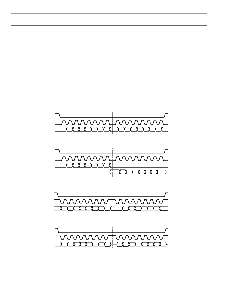
of SCLK. Figure 23 through Figure 26 are useful in understand-
ing the general operation of the AD9952 serial port.
03374-0-008
I
6
I
5
I
4
I
3
I
2
I
1
D
5
D
4
D
3
D
2
D
1
D
0
I
0
D
7
D
6
I
7
INSTRUCTION CYCLE
SCLK
SDIO
DATA TRANSFER CYCLE
CS
Figure 23. Serial Port Write Timing≠Clock Stall Low
03374-0-009
I
6
I
5
I
4
I
3
I
2
I
1
I
0
DON'T CARE
I
7
INSTRUCTION CYCLE
SCLK
SDIO
DATA TRANSFER CYCLE
D
O 5
D
O 4
D
O 3
D
O 2
D
O 1
D
O 0
D
O 7
D
O 6
SDO
CS
Figure 24. 3-Wire Serial Port Read Timing≠Clock Stall Low
03374-0-010
I
6
I
5
I
4
I
3
I
2
I
1
D
5
D
4
D
3
D
2
D
1
D
0
I
0
D
7
D
6
I
7
INSTRUCTION CYCLE
SCLK
SDIO
DATA TRANSFER CYCLE
CS
Figure 25. Serial Port Write Timing≠Clock Stall High
03374-0-011
I
6
I
5
I
4
I
3
I
2
I
1
D
O 5
D
O 4
D
O 3
D
O 2
D
O 1
D
O 0
I
0
D
O 7
D
O 6
I
7
INSTRUCTION CYCLE
SCLK
SDIO
DATA TRANSFER CYCLE
CS
Figure 26. 2-Wire Serial Port Read Timing--Clock Stall High

AD9952
Rev. 0 | Page 23 of 28
INSTRUCTION BYTE
The instruction byte contains the following information:
Table 7.
MSB
D6 D5 D4 D3 D2 D1 LSB
R/W
X X A4 A3 A2 A1 A0
R/W--Bit 7 of the instruction byte determines whether a read
or write data transfer will occur after the instruction byte write.
Logic High indicates read operation. Logic 0 indicates a write
operation.
X, X--Bits 6 and 5 of the instruction byte are Don't Care.
A4, A3, A2, A1, A0--Bits 4, 3, 2, 1, 0 of the instruction byte
determine which register is accessed during the data transfer
portion of the communications cycle.
SERIAL INTERFACE PORT PIN DESCRIPTION
SCLK--Serial Clock. The serial clock pin is used to synchronize
data to and from the AD9952 and to run the internal state
machines. SCLK maximum frequency is 25 MHz.
CSB--Chip Select Bar. CSB is active low input that allows more
than one device on the same serial communications line. The
SDO and SDIO pins will go to a high impedance state when this
input is high. If driven high during any communications cycle,
that cycle is suspended until CS is reactivated low. Chip select
can be tied low in systems that maintain control of SCLK.
SDIO--Serial Data I/O. Data is always written into the AD9952
on this pin. However, this pin can be used as a
bidirectional data line. Bit 7 of Register Address 0x00 controls
the configuration of this pin. The default is Logic 0, which
configures the SDIO pin as bidirectional.
SDO--Serial Data Out. Data is read from this pin for protocols
that use separate lines for transmitting and receiving data. In the
case where the AD9952 operates in a single bidirectional I/O
mode, this pin does not output data and is set to a high imped-
ance state.
IOSYNC--It synchronizes the I/O port state machines without
affecting the addressable register's contents. An active high in-
put on the IOSYNC pin causes the current communication
cycle to abort. After IOSYNC returns low (Logic 0), another
communication cycle may begin, starting with the instruction
byte write.
MSB/LSB TRANSFERS
The AD9952 serial port can support both most significant bit
(MSB) first or least significant bit (LSB) first data formats. This
functionality is controlled by the Control Register 0x00 <8> bit.
The default value of Control Register 0x00 <8> is low (MSB
first). When Control Register 0x00 <8> is set high, the AD9952
serial port is in LSB first format. The instruction byte must be
written in the format indicated by Control Register 0x00 <8>. If
the AD9952 is in LSB first mode, the instruction byte must be
written from least significant bit to most significant bit.
For MSB first operation, the serial port controller will generate
the most significant byte (of the specified register) address first
followed by the next lesser significant byte addresses until the
I/O operation is complete. All data written to (read from) the
AD9952 must be (will be) in MSB first order. If the LSB mode is
active, the serial port controller will generate the least signifi-
cant byte address first followed by the next greater significant byte
addresses until the I/O operation is complete. All data written to
(read from) the AD9952 must be (will be) in LSB first order.
Example Operation
To write the amplitude scale factor register in MSB first format,
apply an instruction byte of 0x02 [serial address is 00010(b)].
From this instruction, the internal controller will generate an
internal byte address of 0x07 (see the register map) for the first
data byte written and an internal address of 0x08 for the next
byte written. Since the amplitude scale factor register is two
bytes wide, this ends the communication cycle.
To write the amplitude scale factor register in LSB first format,
apply an instruction byte of 0x40. From this instruction, the
internal controller will generate an internal byte address of
0x08 (see the register map) for the first data byte written and an
internal address of 0x07for the next byte written. Since the
amplitude scale factor register is two bytes wide, this ends the
communication cycle.
Power-Down Functions of the AD9952
The AD9952 supports an externally controlled or hardware
power-down feature as well as the more common software pro-
grammable power-down bits found in previous ADI DDS products.
The software control power-down allows the DAC, comparator,
PLL, input clock circuitry, and digital logic to be individually
powered down via unique control bits (CFR1<7:4>). With the
exception of CFR1<6>, these bits are not active when the exter-
nally controlled power-down pin (PWRDWNCTL) is high.
External power-down control is supported on the AD9952 via
the PWRDWNCTL input pin. When the PWRDWNCTL input
pin is high, the AD9952 will enter a power-down mode based
on the CFR1<3> bit. When the PWRDWNCTL input pin is low,
the external power-down control is inactive.

AD9952
Rev. 0 | Page 24 of 28
When the CFR1<3> bit is 0 and the PWRDWNCTL input pin is
high, the AD9952 is put into a fast recovery power-down mode.
In this mode, the digital logic and the DAC digital logic are
powered down. The DAC bias circuitry, comparator, PLL, oscil-
lator, and clock input circuitry is not powered down. The com-
parator can be individually powered down by setting the com-
parator power-down bit, CFR1<6> = 1.
When the CFR1<3> bit is high, and the PWRDWNCTL input
pin is high, the AD9952 is put into the full power-down mode.
In this mode, all functions are powered down. This includes the
DAC and PLL, which take a significant amount of time to
power up.
When the PWRDWNCTL input pin is high, the individual
power-down bits (CFR1<7>, <5:4>) are invalid (Don't Care)
and unused. When the PWRDWNCTL input pin is low, the
individual power-down bits control the power-down modes of
operation.
Note that the power-down signals are all designed such that a
Logic 1 indicates the low power mode and a Logic 0 indicates
the active or power-up mode.
Table 8 indicates the logic level for each power-down bit that
drives out of the AD9952 core logic to the analog section and
the digital clock generation section of the chip for the external
power-down operation.
Layout Considerations
For the best performance, the following layout guidelines
should be observed. Always provide the analog power supply
(AVDD) and the digital power supply (DVDD) on separate
supplies, even if just from two different voltage regulators
driven by a common supply. Likewise, the ground connections
(AGND, DGND) should be kept separate as far back to the
source as possible (i.e., separate the ground planes on a local-
ized board, even if the grounds connect to a common point in
the system). Bypass capacitors should be placed as close to the
device pin as possible. Usually, a multitiered bypassing scheme
consisting of a small high frequency capacitor (100 pF) placed
close to the supply pin and progressively larger capacitors (0.1 µF,
10 µF) placed further away from the actual supply source works
best.
Table 8. Power-Down Control Functions
Control Mode
Active
Description
PWRDWNCTL = 0 CFR1<3> Don't Care
Software Control
Digital Power-Down = CFR1<7>
Comparator Power-Down = CFR1<6>
DAC Power-Down = CFR1<5>
Input Clock Power-Down = CFR1<4>
PWRDWNCTL = 1 CFR1<3> = 0
External Control,
Fast Recovery Power-Down Mode
Digital Power-Down = 1'b1
Comparator Power-Down = 1'b0 or CFR1<6>
DAC Power-Down = 1'b0
Input Clock Power-Down = 1'b0
PWRDWNCTL = 1 CFR1<3> = 1
External Control,
Full Power-Down Mode
Digital Power-Down = 1'b1
Comparator Power-Down = 1'b1
DAC Power-Down = 1'b1
Input Clock Power-Down = 1'b1
AD9952
Rev. 0 | Page 25 of 28
SUGGESTED APPLICATION CIRCUITS
03358-0-003
LPF
AD9952
REFCLK
RF/IF INPUT
MODULATED/
DEMODULATED
SIGNAL
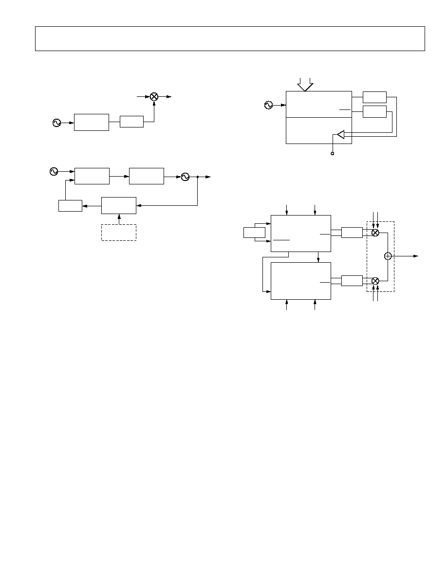
Figure 27. Synchronized LO for Upconversion/Down Conversion
03358-0-004
FILTER
PHASE
COMPARATOR
LOOP
FILTER
AD9952
TUNING
WORLD
REF
SIGNAL
VCO
Figure 28. Digitally Programmable Divide-by-N Function in PLL
03358-0-006
TUNING WORD
CMOS LEVEL CLOCK
AD9952 DDS
AD9952
ON-CHIP
COMPARATOR
IOUT
IOUT
LPF
LPF
Figure 29. Frequency Agile Clock Generator
03358-
0-
005
SAW
CRYSTAL
FREQUENCY
TUNING
WORD
PHASE
OFFSET
WORD 2
I/I-BAR
BASEBAND
FREQUENCY
TUNING
WORD
PHASE
OFFSET
WORD 1
Q/Q-BAR
BASEBAND
SYNC IN
AD9952 DDS
REFCLK
REFCLK
REFCLK
LPF
SYNC OUT
CRYSTAL OUT
AD9952 DDS
IOUT
IOUT
LPF
IOUT
IOUT
RF OUT
Figure 30. Two AD9952s Synchronized to Provide I and
Q Carriers with Independent Phase Offsets for Nulling

AD9952
Rev. 0 | Page 26 of 28
OUTLINE DIMENSIONS
BOTTOM VIEW
(PINS UP)
TOP VIEW
(PINS DOWN)
0.50
BSC
0.27
0.22
0.17
9.00
BSC SQ
7.00
BSC SQ
37
48
1
13
12
24
25
36
VIEW A
0.75
0.60
0.45
VIEW A
1.05
1.00
0.95
7∞
3.5∞
0∞
SEATING
PLANE
0.15
0.05
EXPOSED
PAD
2.00
SQ
1.20
MAX
COMPLIANT TO JEDEC STANDARDS MS-026-ABC
Figure 31. 48-Lead Thin Plastic Quad Flat Package, Exposed Pad [TQFP/EP] (SV-48)--Dimensions shown in millimeters
ESD CAUTION
ESD (electrostatic discharge) sensitive device. Electrostatic charges as high as 4000 V readily accumulate on the
human body and test equipment and can discharge without detection. Although this product features
proprietary ESD protection circuitry, permanent damage may occur on devices subjected to high energy
electrostatic discharges. Therefore, proper ESD precautions are recommended to avoid performance
degradation or loss of functionality.
WARNING--Please note that this device in its current form does not meet Analog Devices' standard requirements for ESD as
measured against the charged device model (CDM). As such, special care should be used when handling this product, especially in
a manufacturing environment. Analog Devices will provide a more ESD-hardy product in the near future at which time this warn-
ing will be removed from this data sheet.
ORDERING GUIDE
Model
Temperature Range
Package Description
Package Outline
AD9952YSV
≠40∞C to +105∞C
48-Lead Thin Plastic Quad Flat Package, Exposed Pad, TQFP/EP
SV-48
AD9952YSV-REEL7
≠40∞C to +105∞C
48-Lead TQFP/EP (500 Piece REEL7)
SV-48
AD9952/PCB
Evaluation
Board

AD9952
Rev. 0 | Page 27 of 28
NOTES

AD9952
Rev. 0 | Page 28 of 28
NOTES
© 2003 Analog Devices, Inc. All rights reserved. Trademarks and regis-
tered trademarks are the property of their respective owners.
D03358-0-12/03(0)