REV. A
Information furnished by Analog Devices is believed to be accurate and
reliable. However, no responsibility is assumed by Analog Devices for its
use, nor for any infringements of patents or other rights of third parties
which may result from its use. No license is granted by implication or
otherwise under any patent or patent rights of Analog Devices.
a
LC
2
MOS Precision
Mini-DIP Analog Switch
ADG419
FEATURES
44 V Supply Maximum Ratings
V
SS
to V
DD
Analog Signal Range
Low On Resistance (< 35 )
Ultralow Power Dissipation (< 35 W)
Fast Transition Time (160 ns max)
Break-Before-Make Switching Action
Plug-In Replacement for DG419
APPLICATIONS
Precision Test Equipment
Precision Instrumentation
Battery Powered Systems
Sample Hold Systems
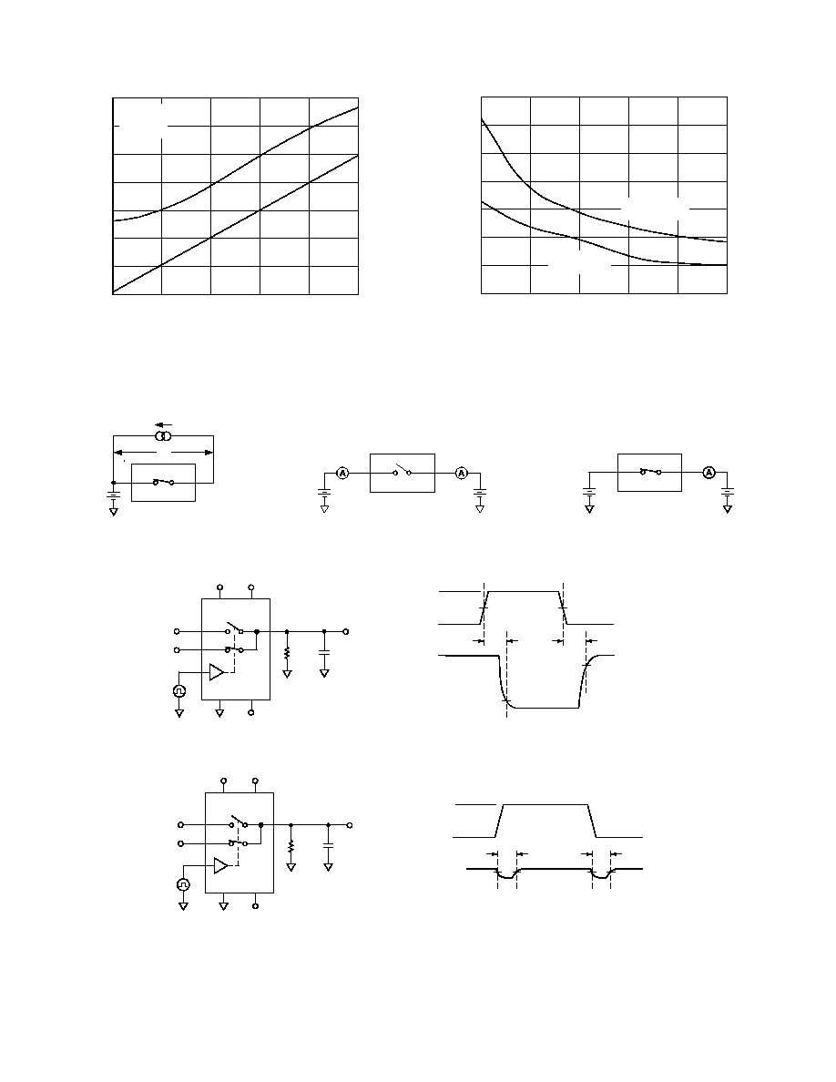
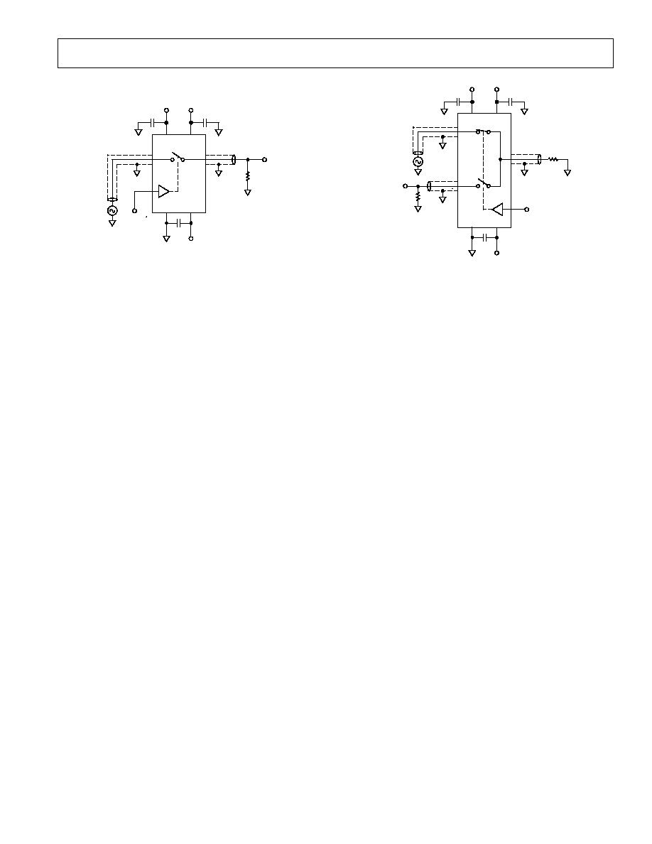
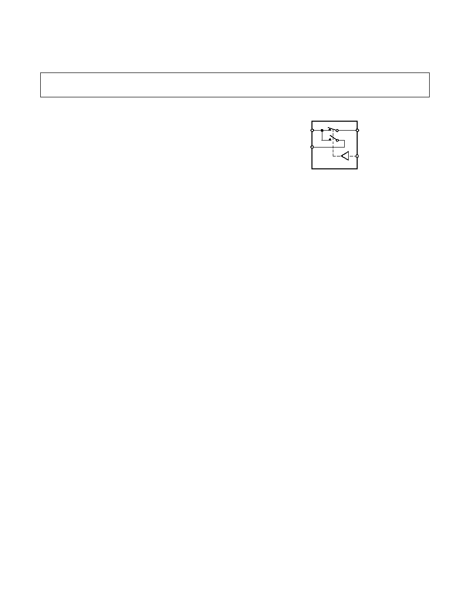
FUNCTIONAL BLOCK DIAGRAM
ADG419
D
S1
S2
IN
SWITCH SHOWN FOR A
LOGIC "1" INPUT
GENERAL DESCRIPTION
The ADG419 is a monolithic CMOS SPDT switch. This
switch is designed on an enhanced LC
2
MOS process that pro-
vides low power dissipation yet gives high switching speed, low
on resistance and low leakage currents.
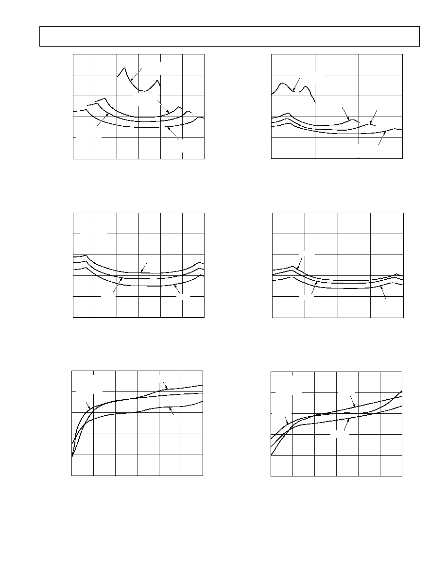
The on resistance profile of the ADG419 is very flat over the full
analog input range, ensuring excellent linearity and low distor-
tion. The part also exhibits high switching speed and high signal
bandwidth. CMOS construction ensures ultralow power dissipa-
tion, making the parts ideally suited for portable and battery
powered instruments.
Each switch of the ADG419 conducts equally well in both
directions when ON and has an input signal range that extends
to the supplies. In the OFF condition, signal levels up to the
supplies are blocked. The ADG419 exhibits break-before-
make switching action.
PRODUCT HIGHLIGHTS
1. Extended Signal Range
The ADG419 is fabricated on an enhanced LC
2
MOS pro-
cess, giving an increased signal range that extends to the
supply rails.
2. Ultralow Power Dissipation
3. Low R
ON
4. Single Supply Operation
For applications where the analog signal is unipolar, the
ADG419 can be operated from a single rail power supply.
The part is fully specified with a single +12 V power supply
and will remain functional with single supplies as low as
+5 V.
One Technology Way, P.O. Box 9106, Norwood, MA 02062-9106, U.S.A.
Tel: 781/329-4700
World Wide Web Site: http://www.analog.com
Fax: 781/326-8703
© Analog Devices, Inc., 1998

REV. A
≠4≠
ADG419
ABSOLUTE MAXIMUM RATINGS
1
(T
A
= +25
∞
C unless otherwise noted)
V
DD
to V
SS
. . . . . . . . . . . . . . . . . . . . . . . . . . . . . . . . . . . +44 V
V
DD
to GND . . . . . . . . . . . . . . . . . . . . . . . . . . ≠0.3 V to +25 V
V
SS
to GND . . . . . . . . . . . . . . . . . . . . . . . . . . +0.3 V to ≠25 V
V
L
to GND . . . . . . . . . . . . . . . . . . . . . . ≠0.3 V to V
DD
+ 0.3 V
Analog, Digital Inputs
2
. . . . . . . . . . . . V
SS
≠ 2 V to V
DD
+ 2 V
or 30 mA, Whichever Occurs First
Continuous Current, S or D . . . . . . . . . . . . . . . . . . . . . 30 mA
Peak Current, S or D . . . . . . . . . . . . . . . . . . . . . . . . . 100 mA
(Pulsed at 1 ms, 10% Duty Cycle Max)
Operating Temperature Range
Industrial (B Version) . . . . . . . . . . . . . . . . . ≠40
∞
C to +85
∞
C
Extended (T Version) . . . . . . . . . . . . . . . . ≠55
∞
C to +125
∞
C
Storage Temperature Range . . . . . . . . . . . . . ≠65
∞
C to +150
∞
C
Junction Temperature . . . . . . . . . . . . . . . . . . . . . . . . . +150
∞
C
Cerdip Package, Power Dissipation . . . . . . . . . . . . . . . 600 mW
JA
, Thermal Impedance . . . . . . . . . . . . . . . . . . . . 110
∞
C/W
Lead Temperature, Soldering (10 sec) . . . . . . . . . . . +300
∞
C
Plastic Package, Power Dissipation . . . . . . . . . . . . . . . 400 mW
JA
, Thermal Impedance . . . . . . . . . . . . . . . . . . . . 100
∞
C/W
Lead Temperature, Soldering (10 sec) . . . . . . . . . . . +260
∞
C
SOIC Package, Power Dissipation . . . . . . . . . . . . . . . . 400 mW
JA
, Thermal Impedance . . . . . . . . . . . . . . . . . . . . 155
∞
C/W
µ
SOIC Package, Power Dissipation . . . . . . . . . . . . . . . 315 mW
JA
, Thermal Impedance . . . . . . . . . . . . . . . . . . . . 205
∞
C/W
Lead Temperature, Soldering
Vapor Phase (60 sec). . . . . . . . . . . . . . . . . . . . . . . +215
∞
C
Infrared (15 sec) . . . . . . . . . . . . . . . . . . . . . . . . . . +220
∞
C
NOTES
1
Stresses above those listed under Absolute Maximum Ratings may cause perma-
nent damage to the device. This is a stress rating only; functional operation of the
device at these or any other conditions above those listed in the operational
sections of this specification is not implied. Exposure to absolute maximum rating
conditions for extended periods may affect device reliability. Only one absolute
maximum rating may be applied at any one time.
2
Overvoltages at IN, S or D will be clamped by internal diodes. Current should be
limited to the maximum ratings given.
C
D
, C
S
(ON)
"ON" switch capacitance.
t
TRANSITION
Delay time between the 50% and 90% points
of the digital inputs and the switch "ON"
condition when switching from one address
state to another.
t
D
"OFF" time or "ON" time measured be-
tween the 90% points of both switches
when switching from one address state
to the other.
V
INL
Maximum input voltage for logic "0."
V
INH
Minimum input voltage for logic "1."
I
INL
(I
INH
)
Input current of the digital input.
Crosstalk
A measure of unwanted signal which is
coupled through from one channel to
another as a result of parasitic capacitance.
Off Isolation
A measure of unwanted signal coupling
through an "OFF" channel.
I
DD
Positive supply current.
I
SS
Negative supply current.
TERMINOLOGY
V
DD
Most positive power supply potential.
V
SS
Most negative power supply potential in dual
supplies. In single supply applications, it
may be connected to GND.
V
L
Logic power supply (+5 V).
GND
Ground (0 V) reference.
S
Source terminal. May be an input or an
output.
D
Drain terminal. May be an input or an
output.
IN
Logic control input.
R
ON
Ohmic resistance between D and S.
I
S
(OFF)
Source leakage current with the switch
"OFF."
I
D
(OFF)
Drain leakage current with the switch
"OFF."
I
D
, I
S
(ON)
Channel leakage current with the switch
"ON."
V
D
(V
S
)
Analog voltage on terminals D, S.
C
S
(OFF)
"OFF" switch source capacitance.
CAUTION
ESD (electrostatic discharge) sensitive device. Electrostatic charges as high as 4000 V readily
accumulate on the human body and test equipment and can discharge without detection.
Although the ADG419 features proprietary ESD protection circuitry, permanent damage may
occur on devices subjected to high energy electrostatic discharges. Therefore, proper ESD
precautions are recommended to avoid performance degradation or loss of functionality.
WARNING!
ESD SENSITIVE DEVICE