REV. B
Information furnished by Analog Devices is believed to be accurate and
reliable. However, no responsibility is assumed by Analog Devices for its
use, nor for any infringements of patents or other rights of third parties
which may result from its use. No license is granted by implication or
otherwise under any patent or patent rights of Analog Devices.
a
ADSP-2106x SHARC
Æ
DSP Microcomputer Family
ADSP-21061/ADSP-21061L
Pin-Compatible with ADSP-21060 (4 Mbit) and
ADSP-21062 (2 Mbit)
Flexible Data Formats and 40-Bit Extended Precision
32-Bit Single-Precision and 40-Bit Extended-Precision
IEEE Floating-Point Data Formats
32-Bit Fixed-Point Data Format, Integer and Fractional,
with 80-Bit Accumulators
Parallel Computations
Single-Cycle Multiply and ALU Operations in Parallel with
Dual Memory Read/Writes and Instruction Fetch
Multiply with Add and Subtract for Accelerated FFT
Butterfly Computation
1024-Point Complex FFT Benchmark: 0.37 ms (18,221 Cycles)
1 Megabit Configurable On-Chip SRAM
Dual-Ported for Independent Access by Core Processor
and DMA
Configurable as 32K Words Data Memory (32-Bit), 16K
Words Program Memory (48-Bit) or Combinations of
Both Up to 1 Mbit
Off-Chip Memory Interfacing
4-Gigawords Addressable (32-Bit Address)
Programmable Wait State Generation, Page-Mode DRAM
Support
SUMMARY
High Performance Signal Computer for Speech, Sound,
Graphics and Imaging Applications
Super Harvard Architecture Computer (SHARC)--
Four Independent Buses for Dual Data, Instructions,
and I/O
32-Bit IEEE Floating-Point Computation Units--
Multiplier, ALU and Shifter
1 Megabit On-Chip SRAM Memory and Integrated I/O
Peripherals--A Complete System-On-A-Chip
Integrated Multiprocessing Features
KEY FEATURES
50 MIPS, 20 ns Instruction Rate, Single-Cycle Instruction
Execution
120 MFLOPS Peak, 80 MFLOPS Sustained Performance
Dual Data Address Generators with Modulo and Bit-
Reverse Addressing
Efficient Program Sequencing with Zero-Overhead
Looping: Single-Cycle Loop Setup
IEEE JTAG Standard 1149.1 Test Access Port and
On-Chip Emulation
240-Lead MQFP Package
225-Ball Plastic Ball Grid Array (PBGA)
SHARC is a registered trademark of Analog Devices, Inc.
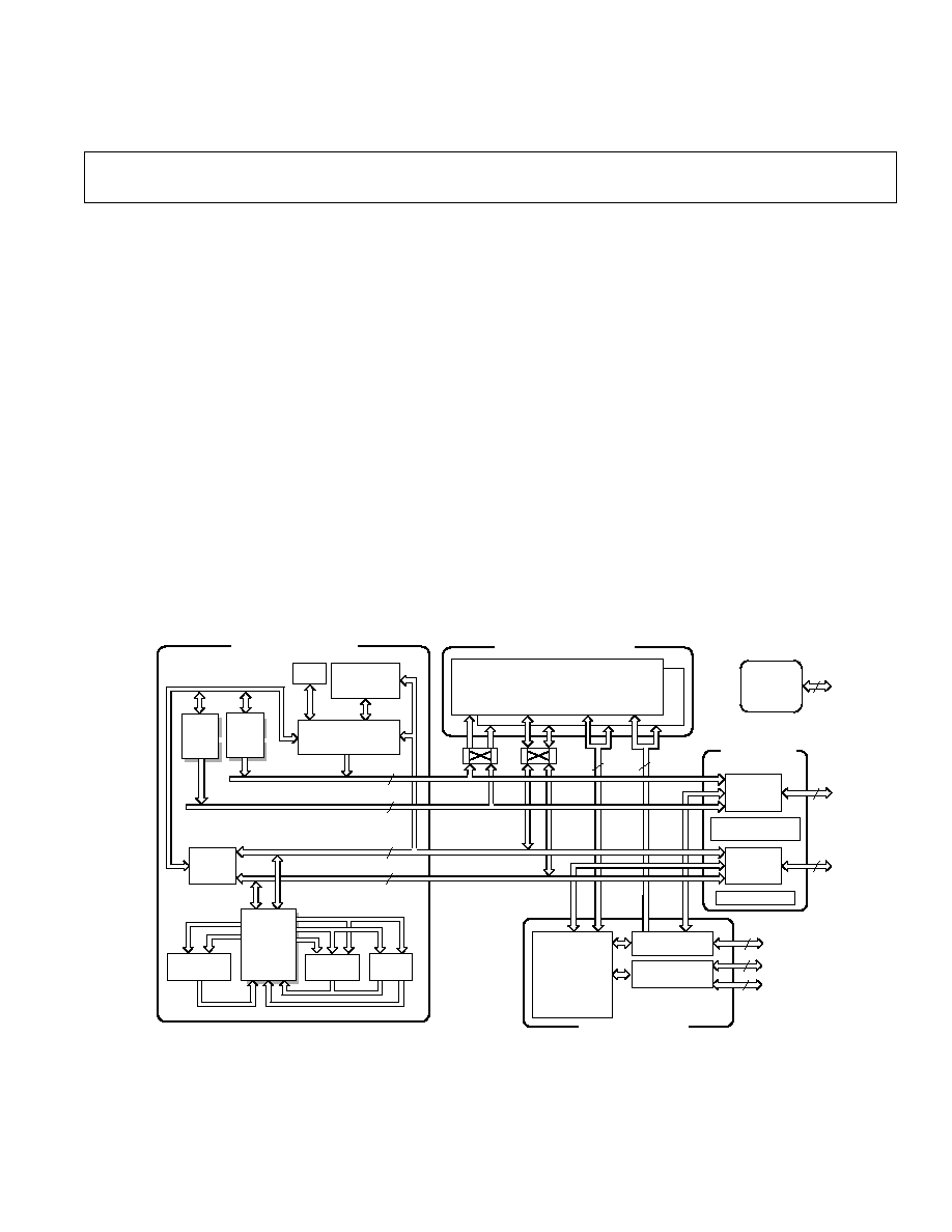
6
4
6
IOP
REGISTERS
(
MEMORY MAPPED)
CONTROL,
STATUS &
DATA BUFFERS
I/O PROCESSOR
TIMER
INSTRUCTION
CACHE
32 x 48-BIT
ADDR
DATA
DATA
DATA
ADDR
ADDR
DATA
ADDR
TWO INDEPENDENT
DUAL-PORTED BLOCKS
PROCESSOR PORT
I/O PORT
BLOCK 0
BLOCK 1
JTAG
TEST &
EMULATION
7
HOST PORT
ADDR BUS
MUX
IOA
17
IOD
48
MULTIPROCESSOR
INTERFACE
DUAL-PORTED SRAM
EXTERNAL
PORT
DATA BUS
MUX
48
32
24
PM ADDRESS BUS
DM ADDRESS BUS
PM DATA BUS
DM DATA BUS
BUS
CONNECT
(PX)
DATA
REGISTER
FILE
16 x 40-BIT
BARREL
SHIFTER
ALU
MULTIPLIER
DAG1
8 x 4 x 32
32
48
40/32
CORE PROCESSOR
DMA
CONTROLLER
PROGRAM
SEQUENCER
DAG2
8 x 4 x 24
SERIAL PORTS
(2)
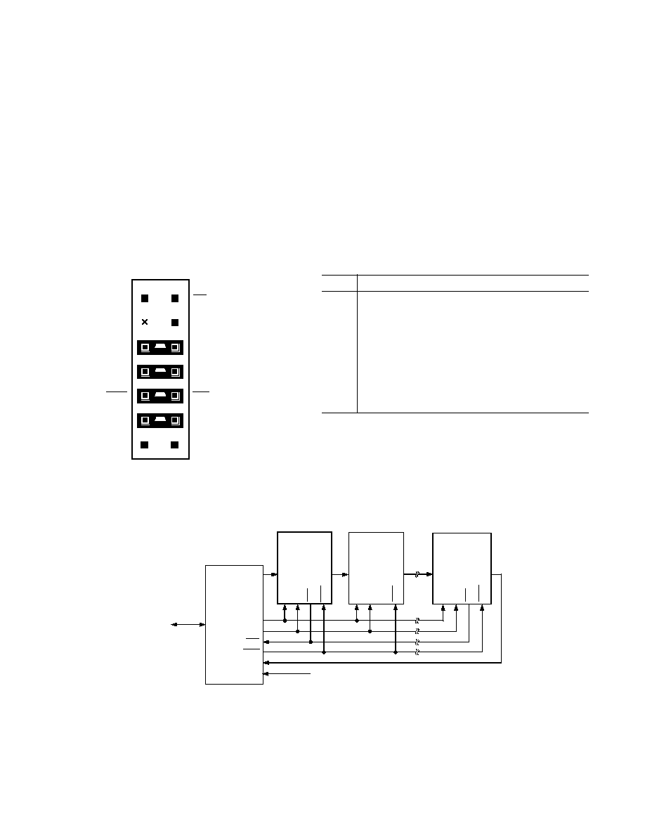
Figure 1. ADSP-21061/ADSP-21061L Block Diagram
One Technology Way, P.O. Box 9106, Norwood, MA 02062-9106, U.S.A.
Tel: 781/329-4700
World Wide Web Site: http://www.analog.com
Fax: 781/326-8703
© Analog Devices, Inc., 2000

≠2≠
ADSP-21061/ADSP-21061L
REV. B
DMA Controller
6 DMA Channels
Background DMA Transfers at 50 MHz, in Parallel with
Full-Speed Processor Execution
Performs Transfers Between ADSP-21061 Internal Memory
and External Memory, External Peripherals, Host
Processor, or Serial Ports
Host Processor Interface
Efficient Interface to 16- and 32-Bit Microprocessors
Host can Directly Read/Write ADSP-21061 Internal Memory
Multiprocessing
Glueless Connection for Scalable DSP Multiprocessing
Architecture
Distributed On-Chip Bus Arbitration for Parallel Bus
Connect of Up To Six ADSP-21061s Plus Host
300 Mbytes/s Transfer Rate Over Parallel Bus
Serial Ports
Two 40 Mbit/s Synchronous Serial Ports
Independent Transmit and Receive Functions
3- to 32-Bit Data Word Width
-Law/A-Law Hardware Companding
TDM Multichannel Mode
Multichannel Signaling Protocol
TABLE OF CONTENTS
GENERAL DESCRIPTION . . . . . . . . . . . . . . . . . . . . . . . . . 3
ADSP-21000 FAMILY CORE ARCHITECTURE . . . . . . . 4
ADSP-21061 FEATURES . . . . . . . . . . . . . . . . . . . . . . . . . . 4
DEVELOPMENT TOOLS . . . . . . . . . . . . . . . . . . . . . . . . . . 8
ADDITIONAL INFORMATION . . . . . . . . . . . . . . . . . . . . . 8
PIN DESCRIPTIONS . . . . . . . . . . . . . . . . . . . . . . . . . . . . . 9
TARGET BOARD CONNECTOR FOR EZ-ICE
Æ
PROBE . . . . . . . . . . . . . . . . . . . . . . . . . . . . . . . . . . . . . . 12
RECOMMENDED OPERATING CONDITIONS (5 V) . 14
ELECTRICAL CHARACTERISTICS (5 V) . . . . . . . . . . . 14
POWER DISSIPATION ADSP-21061 (5 V) . . . . . . . . . . . . 15
RECOMMENDED OPERATING CONDITIONS (3.3 V) 16
ELECTRICAL CHARACTERISTICS (3.3 V) . . . . . . . . . . 16
POWER DISSIPATION ADSP-21061L (3.3 V) . . . . . . . . . 17
ABSOLUTE MAXIMUM RATINGS . . . . . . . . . . . . . . . . 18
TIMING SPECIFICATIONS . . . . . . . . . . . . . . . . . . . . . . . 18
Memory Read--Bus Master . . . . . . . . . . . . . . . . . . . . . . . 21
Memory Write--Bus Master . . . . . . . . . . . . . . . . . . . . . . 22
Synchronous Read/Write--Bus Master . . . . . . . . . . . . . . 23
Synchronous Read/Write--Bus Slave . . . . . . . . . . . . . . . . 25
Multiprocessor Bus Request and Host Bus Request . . . . . 26
Asynchronous Read/Write--Host to ADSP-21061 . . . . . . 28
Three-State Timing--Bus Master, Bus Slave,
HBR, SBTS . . . . . . . . . . . . . . . . . . . . . . . . . . . . . . . . . 30
DMA Handshake . . . . . . . . . . . . . . . . . . . . . . . . . . . . . . . 32
Serial Ports . . . . . . . . . . . . . . . . . . . . . . . . . . . . . . . . . . . . 34
JTAG Test Access Port and Emulation . . . . . . . . . . . . . . . 37
OUTPUT DRIVE CURRENTS . . . . . . . . . . . . . . . . . . . . . 38
POWER DISSIPATION . . . . . . . . . . . . . . . . . . . . . . . . . . . 38
TEST CONDITIONS . . . . . . . . . . . . . . . . . . . . . . . . . . . . 38
ENVIRONMENTAL CONDITIONS . . . . . . . . . . . . . . . . 41
240-LEAD METRIC MQFP PIN CONFIGURATIONS . . 42
OUTLINE DIMENSIONS . . . . . . . . . . . . . . . . . . . . . . 43, 44
ADSP-21061L 225-Ball Plastic Ball Grid Array (PBGA)
Package Pinout . . . . . . . . . . . . . . . . . . . . . . . . . . . . . . . . . 45
225-Ball Plastic Ball Grid Array (PBGA) Package Pinout . . . . . 46
OUTLINE DIMENSIONS . . . . . . . . . . . . . . . . . . . . . . . . . 47
ORDERING GUIDE . . . . . . . . . . . . . . . . . . . . . . . . . . . . . 47
FIGURES
Figure 1. ADSP-21061/ADSP-21061L Block Diagram . . . . 1
Figure 2. ADSP-21061/ADSP-21061L System . . . . . . . . . . . 4
Figure 3. Multiprocessing System . . . . . . . . . . . . . . . . . . . . . 6
Figure 4. ADSP-21061/ADSP-21061L Memory Map . . . . . 7
Figure 5. Target Board Connector For ADSP-21061/
EZ-ICE is a registered trademark of Analog Devices, Inc.
ADSP-21061L EZ-ICE Emulator (Jumpers in Place) . . . 12
Figure 6. JTAG Scan Path Connections for Multiple
ADSP-21061/ADSP-21061L Systems . . . . . . . . . . . . . . . 12
Figure 7. JTAG Clocktree for Multiple ADSP-21061/
ADSP-21061L Systems . . . . . . . . . . . . . . . . . . . . . . . . . . 13
Figure 8. Clock Input . . . . . . . . . . . . . . . . . . . . . . . . . . . . . 19
Figure 9. Reset . . . . . . . . . . . . . . . . . . . . . . . . . . . . . . . . . . 19
Figure 10. Interrupts . . . . . . . . . . . . . . . . . . . . . . . . . . . . . . 20
Figure 11. Timer . . . . . . . . . . . . . . . . . . . . . . . . . . . . . . . . 20
Figure 12. Flags . . . . . . . . . . . . . . . . . . . . . . . . . . . . . . . . . 20
Figure 13. Memory Read--Bus Master . . . . . . . . . . . . . . . . 21
Figure 14. Memory Write--Bus Master . . . . . . . . . . . . . . . 22
Figure 15. Synchronous Read/Write--Bus Master . . . . . . . 24
Figure 16. Synchronous Read/Write--Bus Slave . . . . . . . . . 25
Figure 17. Multiprocessor Bus Request and Host Bus
Request . . . . . . . . . . . . . . . . . . . . . . . . . . . . . . . . . . . . . . 27
Figure 18a. Synchronous REDY Timing . . . . . . . . . . . . . . 28
Figure 18b. Asynchronous Read/Write--Host to
ADSP-21061/ADSP-21061L . . . . . . . . . . . . . . . . . . . . . . 29
Figure 19a. Three-State Timing (Bus Transition Cycle,
SBTS Assertion) . . . . . . . . . . . . . . . . . . . . . . . . . . . . . . . 31
Figure 19b. Three-State Timing (Host Transition Cycle) . . 31
Figure 20. DMA Handshake Timing . . . . . . . . . . . . . . . . . 33
Figure 21. Serial Ports . . . . . . . . . . . . . . . . . . . . . . . . . . . . 35
Figure 22. External Late Frame Sync . . . . . . . . . . . . . . . . . 36
Figure 23. JTAG Test Access Port and Emulation . . . . . . . 37
Figure 24. Output Enable/Disable . . . . . . . . . . . . . . . . . . . 39
Figure 25. Equivalent Device Loading for AC Measurements
(Includes All Fixtures) . . . . . . . . . . . . . . . . . . . . . . . . . . . 39
Figure 26. Voltage Reference Levels for AC Measurements
(Except Output Enable/Disable) . . . . . . . . . . . . . . . . . . . . 39
Figure 27. ADSP-2106x Typical Drive Currents
(V
DD
= 5 V) . . . . . . . . . . . . . . . . . . . . . . . . . . . . . . . . . . . 40
Figure 28. Typical Output Rise Time (10%≠90% V
DD
) vs.
Load Capacitance (V
DD
= 5 V) . . . . . . . . . . . . . . . . . . . . 40
Figure 29. Typical Output Rise Time (0.8 V≠2.0 V) vs. Load
Capacitance (V
DD
= 5 V) . . . . . . . . . . . . . . . . . . . . . . . . . 40
Figure 30. Typical Output Delay or Hold vs. Load Capacitance
(at Maximum Case Temperature) (V
DD
= 5 V) . . . . . . . . 40
Figure 31. ADSP-2106x Typical Drive Currents
(V
DD
= 3.3 V) . . . . . . . . . . . . . . . . . . . . . . . . . . . . . . . . . . 40
Figure 32. Typical Output Rise Time (10%≠90% V
DD
) vs.
Load Capacitance (V
DD
= 3.3 V) . . . . . . . . . . . . . . . . . . . 40
Figure 33. Typical Output Rise Time (0.8 V≠2.0 V) vs. Load
Capacitance (V
DD
= 3.3 V) . . . . . . . . . . . . . . . . . . . . . . . 41
Figure 34. Typical Output Delay or Hold vs. Load Capacitance
(at Maximum Case Temperature) (V
DD
= 3.3 V) . . . . . . . 41

ADSP-21061/ADSP-21061L
≠3≠
REV. B
Figure 1 shows a block diagram of the ADSP-21061/ADSP-
21061L, illustrating the following architectural features:
Computation Units (ALU, Multiplier and Shifter) with a
Shared Data Register File
Data Address Generators (DAG1, DAG2)
Program Sequencer with Instruction Cache
Interval Timer
1 Mbit On-Chip SRAM
External Port for Interfacing to Off-Chip Memory and
Peripherals
Host Port & Multiprocessor Interface
DMA Controller
Serial Ports
JTAG Test Access Port
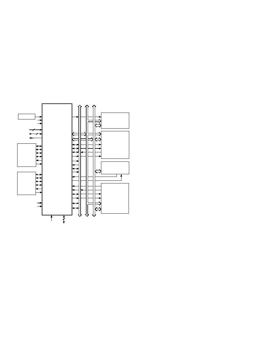
Figure 2 shows a typical single-processor system. A multi-
processing system is shown in Figure 3.
Table I. ADSP-21061/ADSP-21061L Benchmarks (@ 50 MHz)
1024-Pt. Complex FFT
0.37 ms
18,221 Cycles
(Radix 4, with Digit Reverse)
FIR Filter (per Tap)
20 ns
1 Cycle
IIR Filter (per Biquad)
80 ns
4 Cycles
Divide (y/x)
120 ns
6 Cycles
Inverse Square Root (1/
x)
180 ns
9 Cycles
DMA Transfer Rate
300 Mbytes/s
GENERAL NOTE
This data sheet represents production released specifications
for the ADSP-21061 5 V and ADSP-21061L 3.3 V proces-
sors. ADSP-21061 is used throughout this data sheet to refer to
both devices unless expressly noted.
GENERAL DESCRIPTION
The ADSP-21061 is a member of the powerful SHARC family
of floating point processors. The SHARC--Super Harvard
Architecture Computer--are signal processing microcomputers
that offer new capabilities and levels of integration and perfor-
mance. The ADSP-21061 is a 32-bit processor optimized for
high performance DSP applications. The ADSP-21061 com-
bines the ADSP-21000 DSP core with a dual-ported on-chip
SRAM and an I/O processor with a dedicated I/O bus to form a
complete system-in-a-chip.
Fabricated in a high-speed, low-power CMOS process, the
ADSP-21061 has a 20 ns instruction cycle time operating at up
to 50 MIPS. With its on-chip instruction cache, the processor can
execute every instruction in a single cycle. Table I shows perfor-
mance benchmarks for the ADSP-21061/ADSP-21061L.
The ADSP-21061 SHARC
combines a high-performance float-
ing-point DSP core with integrated, on-chip system features,
including a 1 Mbit SRAM memory, host processor interface,
DMA controller, serial ports and parallel bus connectivity for
glueless DSP multiprocessing.
S
Æ
≠4≠
ADSP-21061/ADSP-21061L
REV. B
ADSP-21000 FAMILY CORE ARCHITECTURE
The ADSP-21061 includes the following architectural features
of the ADSP-21000 family core. The ADSP-21061 is code and
function compatible with the ADSP-21060/ADSP-21062 and
the ADSP-21020.
Independent, Parallel Computation Units
The arithmetic/logic unit (ALU), multiplier and shifter all per-
form single-cycle instructions. The three units are arranged in
parallel, maximizing computational throughput. Single multi-
function instructions execute parallel ALU and multiplier op-
erations. These computation units support IEEE 32-bit single-
precision floating-point, extended precision 40-bit floating-
point and 32-bit fixed-point data formats.
3
4
RESET
JTAG
7
ADSP-21061/
ADSP-21061L
BMS
ADDR
31-0
DATA
47-0
CONTROL
ADDRESS
DATA
SERIAL
DEVICE
(OPTIONAL)
SERIAL
DEVICE
(OPTIONAL)
CS
ADDR
DATA
BOOT
EPROM
(OPTIONAL)
ADDR
ACK
CS
MEMORY
AND
PERIPHERALS
(OPTIONAL)
OE
WE
DATA
DMA DEVICE
(OPTIONAL)
DATA
ADDR
DATA
HOST
PROCESSOR
INTERFACE
(OPTIONAL)
1x CLOCK
CS
HBR
HBG
REDY
RD
WR
PAGE
ADRCLK
ACK
MS
3-0
SBTS
SW
BR
1-6
CPA
DMAR
1-2
DMAG
1-2
CLKIN
EBOOT
LBOOT
IRQ
2-0
FLAG
3-0
TIMEXP
TCLK0
RCLK0
TFS0
RSF0
DT0
DR0
TCLK1
RCLK1
TFS1
RSF1
DT1
DR1
RPBA
ID
2-0
TO GND
Figure 2. ADSP-21061/ADSP-21061L System
Data Register File
A general purpose data register file is used for transferring data
between the computation units and the data buses, and for
storing intermediate results. This 10-port, 32-register (16 pri-
mary, 16 secondary) register file, combined with the ADSP-
21000 Harvard architecture, allows unconstrained data flow
between computation units and internal memory.
Single-Cycle Fetch of Instruction and Two Operands
The ADSP-21061 features an enhanced Harvard architecture in
which the data memory (DM) bus transfers data and the pro-
gram memory (PM) bus transfers both instructions and data
(see Figure 1). With its separate program and data memory
buses and on-chip instruction cache, the processor can simulta-
neously fetch two operands and an instruction (from the cache),
all in a single cycle.
Instruction Cache
The ADSP-21061 includes an on-chip instruction cache that
enables three-bus operation for fetching an instruction and two
data values. The cache is selective--only the instructions whose
fetches conflict with PM bus data accesses are cached. This
allows full-speed execution of core, looped operations such as
digital filter multiply-accumulates and FFT butterfly processing.
Data Address Generators with Hardware Circular Buffers
The ADSP-21061's two data address generators (DAGs) imple-
ment circular data buffers in hardware. Circular buffers allow
efficient programming of delay lines and other data structures
required in digital signal processing, and are commonly used in
digital filters and Fourier transforms. The ADSP-21061 two
DAGs contain sufficient registers to allow the creation of up to
32 circular buffers (16 primary register sets, 16 secondary). The
DAGs automatically handle address pointer wraparound, reduc-
ing overhead, increasing performance and simplifying imple-
mentation. Circular buffers can start and end at any memory
location.
Flexible Instruction Set
The 48-bit instruction word accommodates a variety of parallel
operations, for concise programming. For example, the ADSP-
21061 can conditionally execute a multiply, an add, a subtract
and a branch, all in a single instruction.
ADSP-21061 FEATURES
Augmenting the ADSP-21000 family core, the ADSP-21061
adds the following architectural features:
Dual-Ported On-Chip Memory
The ADSP-21061 contains 1 megabit of on-chip SRAM, orga-
nized as two banks of 0.5 Mbits each. Each bank has eight 16-
bit columns with 4K 16-bit words per column. Each memory
block is dual-ported for single-cycle, independent accesses by
the core processor and I/O processor or DMA controller. The
dual-ported memory and separate on-chip buses allow two data
transfers from the core and one from I/O, all in a single cycle
(see Figure 4 for the ADSP-21061 Memory Map).
On the ADSP-21061, the memory can be configured as a maxi-
mum of 32K words of 32-bit data, 64K words for 16-bit data,
16K words of 48-bit instructions (and 40-bit data) or combina-
tions of different word sizes up to 1 megabit. All the memory
can be accessed as 16-bit, 32-bit or 48-bit.
A 16-bit floating-point storage format is supported that effec-
tively doubles the amount of data that may be stored on chip.
Conversion between the 32-bit floating-point and 16-bit floating-
point formats is done in a single instruction.
While each memory block can store combinations of code and
data, accesses are most efficient when one block stores data,
using the DM bus for transfers, and the other block stores in-
structions and data, using the PM bus for transfers. Using the
DM and PM buses in this way, with one dedicated to each
memory block, assures single-cycle execution with two data
transfers. In this case, the instruction must be available in the
cache. Single-cycle execution is also maintained when one of the
data operands is transferred to or from off-chip, via the ADSP-
21061's external port.

ADSP-21061/ADSP-21061L
≠5≠
REV. B
Off-Chip Memory and Peripherals Interface
The ADSP-21061's external port provides the processor's inter-
face to off-chip memory and peripherals. The 4-gigaword off-
chip address space is included in the ADSP-21061's unified
address space. The separate on-chip buses--for program
memory, data memory and I/O--are multiplexed at the external
port to create an external system bus with a single 32-bit address
bus and a single 48-bit (or 32-bit) data bus. The on-chip
Super Harvard Architecture provides three-bus performance,
while the off-chip unified address space gives flexibility to the
designer.
Addressing of external memory devices is facilitated by on-chip
decoding of high order address lines to generate memory bank
select signals. Separate control lines are also generated for sim-
plified addressing of page-mode DRAM. The ADSP-21061
provides programmable memory wait states and external memory
acknowledge controls to allow interfacing to DRAM and peripher-
als with variable access, hold and disable time requirements.
Host Processor Interface
The ADSP-21061's host interface allows easy connection to
standard microprocessor buses, both 16-bit and 32-bit, with
little additional hardware required. Asynchronous transfers at
speeds up to the full clock rate of the processor are supported.
The host interface is accessed through the ADSP-21061's exter-
nal port and is memory-mapped into the unified address space.
Two channels of DMA are available for the host interface; code
and data transfers are accomplished with low software overhead.
The host processor requests the ADSP-21061's external bus
with the host bus request (
HBR), host bus grant (HBG) and
ready (REDY) signals. The host can directly read and write the
internal memory of the ADSP-21061, and can access the
DMA channel setup and mailbox registers. Vector interrupt
support is provided for efficient execution of host commands.
DMA Controller
The ADSP-21061's on-chip DMA controller allows zero-
overhead, nonintrusive data transfers without processor inter-
vention. The DMA controller operates independently and
invisibly to the processor core, allowing DMA operations to
occur while the core is simultaneously executing its program
instructions.
DMA transfers can occur between the ADSP-21061's internal
memory and either external memory, external peripherals, or a
host processor. DMA transfers can also occur between the
ADSP-21061's internal memory and its serial ports. DMA
transfers between external memory and external peripheral
devices are another option. External bus packing to 16-, 32-
or 48-bit words is performed during DMA transfers.
Six channels of DMA are available on the ADSP-21061--four
via the serial ports, and two via the processor's external port (for
either host processor, other ADSP-21061s, memory or I/O
transfers). Programs can be downloaded to the ADSP-21061
using DMA transfers. Asynchronous off-chip peripherals can
control two DMA channels using DMA Request/Grant lines
(
DMAR
1-2
,
DMAG
1-2
). Other DMA features include interrupt
generation upon completion of DMA transfers and DMA chain-
ing for automatic linked DMA transfers.
Serial Ports
The ADSP-21061 features two synchronous serial ports that
provide an inexpensive interface to a wide variety of digital and
mixed-signal peripheral devices. The serial ports can operate at
the full clock rate of the processor, providing each with a maxi-
mum data rate of 40 Mbit/s. Independent transmit and receive
functions provide greater flexibility for serial communications.
Serial port data can be automatically transferred to and from
on-chip memory via DMA. Each of the serial ports offers TDM
multichannel mode.
The serial ports can operate with little-endian or big-endian
transmission formats, with word lengths selectable from three
bits to 32 bits. They offer selectable synchronization and trans-
mit modes as well as optional
µ-law or A-law companding.
Serial port clocks and frame syncs can be internally or externally
generated. The serial ports also include keyword and keymask
features to enhance interprocessor communication.
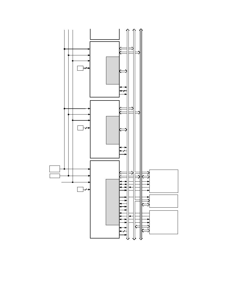
Multiprocessing
The ADSP-21061 offers powerful features tailored to multipro-
cessing DSP systems. The unified address space allows direct
interprocessor accesses of each ADSP-21061's internal memory.
Distributed bus arbitration logic is included on-chip for simple,
glueless connection of systems containing up to six ADSP-21061s
and a host processor. Master processor changeover incurs only
one cycle of overhead. Bus arbitration is selectable as either
fixed or rotating priority. Bus lock allows indivisible read-modify-
write sequences for semaphores. A vector interrupt is provided
for interprocessor commands. Maximum throughput for inter-
processor data transfer is 500 Mbytes/sec over the external port.
Broadcast writes allow simultaneous transmission of data to
all ADSP-21061s and can be used to implement reflective
semaphores.
Program Booting
The internal memory of the ADSP-21061 can be booted at
system power-up from either an 8-bit EPROM or a host proces-
sor. Selection of the boot source is controlled by the
BMS (Boot
Memory Select), EBOOT (EPROM Boot), and LBOOT (Host
Boot) pins. 32-bit and 16-bit host processors can be used for
booting. See the
BMS pin in the Pin Function Descriptions
section of this data sheet.
≠6≠
ADSP-21061/ADSP-21061L
REV. B
ADDR
31-0
DATA
47-0
CONTROL
ADSP-2106x #1
5
CONTROL
ADSP-2106x #2
ADDR
31-0
DATA
47-0
CONTROL
ADSP-2106x #3
5
3
011
ID
2-0
RPBA
CLKIN
ADSP-2106x #6
ADSP-2106x #5
ADSP-2106x #4
CONTROL
ADDRESS
DATA
1x
CLOCK
ADDR
DATA
HOST
PROCESSOR
INTERFACE
(OPTIONAL)
GLOBAL
MEMORY
AND
PERIPHERALS
(OPTIONAL)
BOOT
EPROM
(OPTIONAL)
ADDR
31-0
DATA
47-0
5
3
010
ID
2-0
RPBA
CLKIN
ID
2-0
RPBA
CLKIN
3
001
CONTROL
ADDRESS
DATA
RESET
RESET
RESET
RESET
CPA
BR
1-2
,
BR
4-6
BR
3
CPA
BR
1
,
BR
3-6
BR
2
CPA
BR
2-6
BR
1
RD
WR
ACK
MS
3-0
BMS
PAGE
SBTS
SW
ADRCLK
CS
HBR
HBG
REDY
CS
ADDR
DATA
ADDR
DATA
OE
WE
ACK
CS
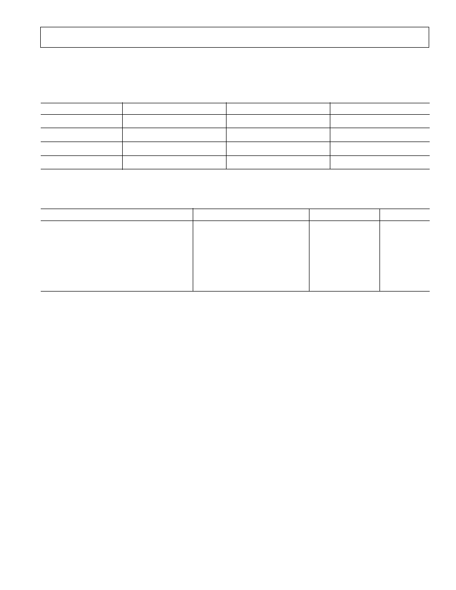
Figure 3. Multiprocessing System
ADSP-21061/ADSP-21061L
≠7≠
REV. B
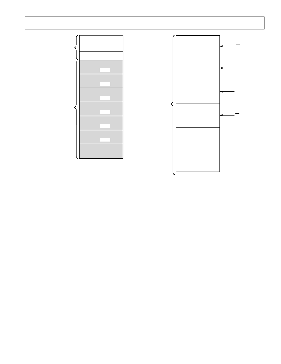
IOP REGISTERS
NORMAL WORD ADDRESSING
0x0000 0000
0x0002 0000
0x0004 0000
0x0008 0000
0x0010 0000
0x0018 0000
0x0020 0000
0x0028 0000
0x0030 0000
0x0038 0000
INTERNAL
MEMORY
SPACE
0x003F FFFF
SHORT WORD ADDRESSING
INTERNAL MEMORY SPACE
OF ADSP-2106x
WITH ID=010
INTERNAL MEMORY SPACE
OF ADSP-2106x
WITH ID=001
INTERNAL MEMORY SPACE
OF ADSP-2106x
WITH ID=011
INTERNAL MEMORY SPACE
OF ADSP-2106x
WITH ID=100
INTERNAL MEMORY SPACE
OF ADSP-2106x
WITH ID=101
INTERNAL MEMORY SPACE
OF ADSP-2106x
WITH ID=110
BROADCAST WRITE
TO ALL
ADSP-2106xs
MULTIPROCESSOR
MEMORY SPACE
NORMAL WORD ADDRESSING: 32-BIT DATA WORDS
48-BIT INSTRUCTION WORDS
SHORT WORD ADDRESSING: 16-BIT DATA WORDS
BANK 0
0x0040 0000
0xFFFF FFFF
BANK 1
BANK 2
DRAM
(OPTIONAL)
BANK 3
NONBANKED
MS
3
BANK SIZE IS
SELECTED BY
MSIZE BIT FIELD OF
SYSCON
REGISTER.
EXTERNAL
MEMORY
SPACE
MS
2
MS
1
MS
0
Figure 4. ADSP-21061/ADSP-21061L Memory Map

≠8≠
ADSP-21061/ADSP-21061L
REV. B
Porting Code from ADSP-21060 or ADSP-21062 to the
ADSP-21061
The ADSP-21061 is pin compatible with the ADSP-21060/
ADSP-21061/ADSP-21062 processors. The ADSP-21061 pins
that correspond to the Link Port pins of the ADSP-21060/
ADSP-21062 are no-connects.
The ADSP-21061 is object code compatible with the ADSP-
21060/ADSP-21062 except for the following functional
changes:
The ADSP-21061 memory is organized into two blocks
with eight columns that are 4K deep per block. The
ADSP-21060/ADSP-21062 memory has 16 columns per block.
Link port functions are not available.
Handshake external port DMA pins
DMAR2 and DMAG2
are assigned to external port DMA Channel 6 instead of
Channel 8.
2-D DMA capability of the SPORT is not available.
The modify registers in SPORT DMA are not programmable.
On the ADSP-21061, Block 0 starts at the beginning of internal
memory, normal word address 0x0002 0000. Block 1 starts at
the end of Block 0, with contiguous addresses. The remaining
addresses in internal memory are divided into blocks that alias
into Block 1. This allows any code or data stored in Block 1 on
the ADSP-21062 to retain the same addresses on the ADSP-
21061--these addresses will alias into the actual Block 1 of each
processor.
If you develop your application using the ADSP-21062, but will
migrate to the ADSP-21061, use only the first eight columns of
each memory bank. Limit your application to 8K of instructions
or up to 16K of data in each bank of the ADSP-21062, or any
combinations of instructions or data that does not exceed the
memory bank.
DEVELOPMENT TOOLS
The ADSP-21061 is supported with a complete set of software
and hardware development tools, including an EZ-ICE
In-
Circuit Emulator, EZ-Kit Lite, and development software. The
SHARC
EZ-Kit Lite (ADDS-2106x-EZ-Lite) is a complete low
cost package for DSP evaluation and prototyping. The EZ-Kit
Lite contains an evaluation board with an ADSP-21061 (5 V)
processor and provides a serial connection to your PC. The EZ-
Kit Lite also includes an optimizing compiler, assembler, in-
struction level simulator, run-time libraries, diagnostic utilities
and a complete set of example programs.
CBUG and SHARCPAC are trademarks of Analog Devices, Inc.
The same EZ-ICE hardware can be used for the ADSP-21060/
ADSP-21062, to fully emulate the ADSP-21061, with the excep-
tion of displaying and modifying the two new SPORTS
registers. The emulator will not display these two registers,
but your code can use them.
Analog Devices ADSP-21000 Family Development Software
includes an easy to use Assembler based on an algebraic syntax,
Assembly Library/Librarian, Linker, instruction-level Simulator,
an ANSI C optimizing Compiler, the CBUGTM C Source--
Level Debugger and a C Runtime Library including DSP and
mathematical functions. The Optimizing Compiler includes
Numerical C extensions based on the work of the ANSI Nu-
merical C Extensions Group. Numerical C provides extensions
to the C language for array selections, vector math operations,
complex data types, circular pointers and variably dimensioned
arrays. The ADSP-21000 Family Development Software is
available for both the PC and Sun platforms.
The EZ-ICE
Emulator uses the IEEE 1149.1 JTAG test access
port of the ADSP-21061 processor to monitor and control the
target board processor during emulation. The EZ-ICE
provides
full-speed emulation, allowing inspection and modification of
memory, registers, and processor stacks. Nonintrusive in-circuit
emulation is assured by the use of the processor's JTAG inter-
face--the emulator does not affect target system loading or
timing.
Further details and ordering information are available in the
ADSP-21000 Family Hardware and Software Development Tools
data sheet (ADDS-210xx-TOOLS). This data sheet can be
requested from any Analog Devices sales office or distributor.
In addition to the software and hardware development tools
available from Analog Devices, third parties provide a wide
range of tools supporting the SHARC
processor family. Hard-
ware tools include SHARC
PC plug-in cards multiprocessor
SHARC
VME boards, and daughter and modules with multiple
SHARCs and additional memory. These modules are based on
the SHARCPACTM module specification. Third Party software
tools include an Ada compiler, DSP libraries, operating systems
and block diagram design tools.
ADDITIONAL INFORMATION
This data sheet provides a general overview of the ADSP-21061
architecture and functionality. For detailed information on the
ADSP-21000 Family core architecture and instruction set, refer to
the ADSP-2106x SHARC User's Manual, Second Edition.

ADSP-21061/ADSP-21061L
≠9≠
REV. B
PIN DESCRIPTIONS
ADSP-21061 pin definitions are listed below. Inputs identified
as synchronous (S) must meet timing requirements with respect
to CLKIN (or with respect to TCK for TMS, TDI). Inputs
identified as asynchronous (A) can be asserted asynchronously
to CLKIN (or to TCK for
TRST).
Unused inputs should be tied or pulled to IVDD or IGND,
except for ADDR
31-0
, DATA
47-0
, FLAG
3-0
,
SW and inputs that
have internal pull-up or pull-down resistors (
CPA, ACK, DTx,
DRx, TCLKx, RCLKx, TMS and TDI)--these pins can be left
floating. These pins have a logic-level hold circuit that prevents
the input from floating internally.
I = Input
S = Synchronous
P = Power Supply
(O/D) = Open Drain
O = Output
A = Asynchronous
G = Ground
(A/D) = Active Drive
T = Three-State (when
SBTS is asserted, or when the
ADSP-2106x is a bus slave)
PIN FUNCTION DESCRIPTIONS
Pin
Type
Function
ADDR
31-0
I/O/T
External Bus Address. The ADSP-21061 outputs addresses for external memory and peripherals
on these pins. In a multiprocessor system the bus master outputs addresses for read/writes of the
internal memory or IOP registers of other ADSP-2106xs. The ADSP-21061 inputs addresses when a
host processor or multiprocessing bus master is reading or writing its internal memory or IOP registers.
DATA
47-0
I/O/T
External Bus Data. The ADSP-21061 inputs and outputs data and instructions on these pins.
The external data bus transfers 32-bit single-precision floating-point data and 32-bit fixed-point
data over Bits 47-16. 40-bit extended-precision floating-point data is transferred over Bits 47-8 of
the bus. 16-bit short word data is transferred over Bits 31-16 of the bus. Pull-up resistors on un-
used DATA pins are not necessary.
MS
3-0
O/T
Memory Select Lines. These lines are asserted (low) as chip selects for the corresponding banks
of external memory. Memory bank size must be defined in the ADSP-21061's system control regis-
ter (SYSCON). The
MS
3-0
lines are decoded memory address lines that change at the same time as
the other address lines. When no external memory access is occurring the
MS
3-0
lines are inactive;
they are active, however, when a conditional memory access instruction is executed, whether or not the
condition is true.
MS
0
can be used with the PAGE signal to implement a bank of DRAM memory
(Bank 0). In a multiprocessor system the
MS
3-0
lines are output by the bus master.
RD
I/O/T
Memory Read Strobe. This pin is asserted (low) when the ADSP-21061 reads from external
memory devices or from the internal memory of other ADSP-21061s. External devices (including
other ADSP-21061s) must assert
RD to read from the ADSP-21061's internal memory. In a multi-
processor system
RD is output by the bus master and is input by all other ADSP-21061s.
WR
I/O/T
Memory Write Strobe. This pin is asserted (low) when the ADSP-21061 writes to external memory
devices or to the internal memory of other ADSP-21061s. External devices must assert
WR to write to
the ADSP-21061's internal memory. In a multiprocessor system
WR is output by the bus master and is
input by all other ADSP-21061s.
PAGE
O/T
DRAM Page Boundary. The ADSP-21061 asserts this pin to signal that an external DRAM page
boundary has been crossed. DRAM page size must be defined in the ADSP-21061's memory con-
trol register (WAIT). DRAM can only be implemented in external memory Bank 0; the PAGE
signal can only be activated for Bank 0 accesses. In a multiprocessor system PAGE is output by the
bus master.
ADRCLK
O/T
Address Clock for synchronous external memories. Addresses on ADDR
31-0
are valid before the
rising edge of ADRCLK. In a multiprocessing system ADRCLK is output by the bus master.
SW
I/O/T
Synchronous Write Select. This signal is used to interface the ADSP-2106x to synchronous memory
devices (including other ADSP-21061s). The ADSP-21061 asserts
SW (low) to provide an early indica-
tion of an impending write cycle, which can be aborted if
WR is not later asserted (e.g. in a conditional
write instruction). In a multiprocessor system,
SW is output by the bus master and is input by all other
ADSP-21061s to determine if the multiprocessor memory access is a read or write.
SW is asserted at the
same time as the address output. A host processor using synchronous writes must assert this pin when
writing to the ADSP-21061(s).
ACK
I/O/S
Memory Acknowledge. External devices can deassert ACK (low) to add wait states to an external
memory access. ACK is used by I/O devices, memory controllers or other peripherals to hold off
completion of an external memory access. The ADSP-21061 deasserts ACK as an output to add
wait states to a synchronous access of its internal memory. In a multiprocessor system, a slave
ADSP-21061 deasserts the bus master's ACK input to add wait state(s) to an access of its internal
memory. The bus master has a keeper latch on its ACK pin that maintains the input at the level it
was last driven to.

≠10≠
ADSP-21061/ADSP-21061L
REV. B
Pin
Type
Function
SBTS
I/S
Suspend Bus Three-State. External devices can assert
SBTS (low) to place the external bus address,
data, selects, and strobes in a high impedance state for the following cycle. If the ADSP-21061
attempts to access external memory while
SBTS is asserted, the processor will halt and the memory
access will not be completed until
SBTS is deasserted. SBTS should only be used to recover from
PAGE faults or host processor/ADSP-21061 deadlock.
IRQ
2-0
I/A
Interrupt Request Lines. May be either edge-triggered or level-sensitive.
FLAG
3-0
I/O/A
Flag Pins. Each is configured via control bits as either an input or an output. As an input, it can be
tested as a condition. As an output, it can be used to signal external peripherals.
TIMEXP
O
Timer Expired. Asserted for four cycles when the timer is enabled and TCOUNT decrements to
zero.
HBR
I/A
Host Bus Request. Must be asserted by a host processor to request control of the ADSP-21061's
external bus. When
HBR is asserted in a multiprocessing system, the ADSP-21061 that is bus master
will relinquish the bus and assert
HBG. To relinquish the bus, the ADSP-21061 places the address,
data, select, and strobe lines in a high impedance state.
HBR has priority over all ADSP-21061 bus
requests (
BR
6-1
) in a multiprocessing system.
HBG
I/O
Host Bus Grant. Acknowledges an
HBR bus request, indicating that the host processor may take
control of the external bus.
HBG is asserted (held low) by the ADSP-21061 until HBR is released. In a
multiprocessing system,
HBG is output by the ADSP-21061 bus master and is monitored by all others.
CS
I/A
Chip Select. Asserted by host processor to select the ADSP-21061.
REDY (O/D)
O
Host Bus Acknowledge. The ADSP-2106x deasserts REDY (low) to add wait states to an asynchro-
nous access of its internal memory or IOP registers by a host. Open drain output (O/D) by default; can
be programmed in ADREDY bit of SYSCON register to be active drive (A/D). REDY will only be
output if the
CS and HBR inputs are asserted.
DMAR1
I/A
DMA Request 1 (DMA Channel 7).
DMAR2
I/A
DMA Request 2 (DMA Channel 6).
DMAG1
O/T
DMA Grant 1 (DMA Channel 7).
DMAG2
O/T
DMA Grant 2 (DMA Channel 6).
BR
6-1
I/O/S
Multiprocessing Bus Requests. Used by multiprocessing ADSP-21061s to arbitrate for bus master-
ship. An ADSP-21061 only drives its own
BRx line (corresponding to the value of its ID
2-0
inputs) and
monitors all others. In a multiprocessor system with less than six ADSP-21061s, the unused
BRx pins
should be tied high; the processor's own
BRx line must not be tied high or low because it is an output.
ID
2-0
I
Multiprocessing ID. Determines which multiprocessing bus request (
BR1≠BR6) is used by ADSP-
21061. ID = 001 corresponds to
BR1, ID = 010 corresponds to BR2, etc. ID = 000 in single-processor
systems. These lines are a system configuration selection which should be hardwired or only changed at
reset.
RPBA
I/S
Rotating Priority Bus Arbitration Select. When RPBA is high, rotating priority for multiprocessor
bus arbitration is selected. When RPBA is low, fixed priority is selected. This signal is a system con-
figuration selection which must be set to the same value on every ADSP-21061. If the value of RPBA is
changed during system operation, it must be changed in the same CLKIN cycle on every ADSP-21061.
CPA (O/D)
I/O
Core Priority Access. Asserting its
CPA pin allows the core processor of an ADSP-21061 bus slave
to interrupt background DMA transfers and gain access to the external bus.
CPA is an open drain
output that is connected to all ADSP-2106Ls in the system. The
CPA pin has an internal 5 k
pull-up
resistor. If core access priority is not required in a system, the
CPA pin should be left unconnected.
DTx
O
Data Transmit (Serial Ports 0, 1). Each DT pin has a 50 k
internal pull-up resistor.
DRx
I
Data Receive (Serial Ports 0, 1). Each DR pin has a 50 k
internal pull-up resistor.
TCLKx
I/O
Transmit Clock (Serial Ports 0, 1). Each TCLK pin has a 50 k
internal pull-up resistor.
RCLKx
I/O
Receive Clock (Serial Ports 0, 1). Each RCLK pin has a 50 k
internal pull-up resistor.

ADSP-21061/ADSP-21061L
≠11≠
REV. B
Pin
Type
Function
TFSx
I/O
Transmit Frame Sync (Serial Ports 0, 1).
RFSx
I/O
Receive Frame Sync (Serial Ports 0, 1).
EBOOT
I
EPROM Boot Select. When EBOOT is high, the ADSP-21061 is configured for booting from an 8-
bit EPROM. When EBOOT is low, the LBOOT and
BMS inputs determine booting mode. See table
below. This signal is a system configuration selection which should be hardwired.
LBOOT
I
Link Boot--Must be tied to GND.
BMS
I/O/T*
Boot Memory Select. Output: Used as chip select for boot EPROM devices (when EBOOT = 1,
LBOOT = 0). In a multiprocessor system,
BMS is output by the bus master. Input: When low, indi-
cates that no booting will occur and that ADSP-21061 will begin executing instructions from external
memory. See table below. This input is a system configuration selection which should be hardwired.
*Three-statable only in EPROM boot mode (when
BMS is an output).
EBOOT
LBOOT
BMS
Booting Mode
1
0
Output
EPROM (Connect
BMS to EPROM chip select.)
0
0
1 (Input)
Host Processor
0
0
0 (Input)
No Booting. Processor executes from external memory.
CLKIN
I
Clock In. External clock input to the ADSP-21061. The instruction cycle rate is equal to CLKIN.
CLKIN may not be halted, changed, or operated below the specified frequency.
RESET
I/A
Processor Reset. Resets the ADSP-21061 to a known state and begins execution at the program
memory location specified by the hardware reset vector address. This input must be asserted (low) at
power-up.
TCK
I
Test Clock (JTAG). Provides an asynchronous clock for JTAG boundary scan.
TMS
I/S
Test Mode Select (JTAG). Used to control the test state machine. TMS has a 20 k
internal pull-up
resistor.
TDI
I/S
Test Data Input (JTAG). Provides serial data for the boundary scan logic. TDI has a 20 k
internal
pull-up resistor.
TDO
O
Test Data Output (JTAG). Serial scan output of the boundary scan path.
TRST
I/A
Test Reset (JTAG). Resets the test state machine.
TRST must be asserted (pulsed low) after power-
up or held low for proper operation of the ADSP-21061.
TRST has a 20 k
internal pull-up resistor.
EMU
O
Emulation Status. Must be connected to the ADSP-21061 EZ-ICE
target board connector only.
ICSA
O
Reserved, leave unconnected.
VDD
P
Power Supply; nominally +3.3 V dc for ADSP-21061L, +5.0 V dc for ADSP-21061.
GND
G
Power Supply Return.
NC
Do Not Connect. Reserved pins which must be left open and unconnected.
≠12≠
ADSP-21061/ADSP-21061L
REV. B
The 14-pin, 2-row pin strip header is keyed at the Pin 3 location --
Pin 3 must be removed from the header. The pins must be
0.025 inch square and at least 0.20 inch in length. Pin spacing
should be 0.1
◊ 0.1 inches. Pin strip headers are available from
vendors such as 3M, McKenzie and Samtec.
The BTMS, BTCK,
BTRST and BTDI signals are provided so
the test access port can also be used for board-level testing.
When the connector is not being used for emulation, place
jumpers between the Bxxx pins and the xxx pins. If the test
access port will not be used for board testing, tie
BTRST to GND
and tie or pull BTCK up to VDD. The
TRST pin must be
asserted after power-up (through
BTRST on the connector) or
held low for proper operation of the ADSP-2106x. None of the
Bxxx pins (Pins 5, 7, 9, 11) are connected on the EZ-ICE
probe.
The JTAG signals are terminated on the EZ-ICE probe as
follows:
Signal
Termination
TMS
Driven through 22
Resistor (16 mA Driver)
TCK
Driven at 10 MHz through 22
Resistor (16 mA
Driver)
TRST* Active Low Driven through 22
Resistor (16 mA
Driver) (Pulled Up by On-Chip 20 k
Resistor)
TDI
Driven by 22
Resistor (16 mA Driver)
TDO
One TTL Load, Split Termination (160/220)
CLKIN One TTL Load, Split Termination (160/220)
EMU
Active Low 4.7 k
Pull-Up Resistor, One TTL Load
(Open-Drain Output from the DSP)
*
TRST is driven low until the EZ-ICE
probe is turned on by the emulator at
software start-up. After software start-up,
TRST is driven high.
Figure 6 shows JTAG scan path connections for systems that
contain multiple ADSP-2106x processors.
TARGET BOARD CONNECTOR FOR EZ-ICE
PROBE
The ADSP-2106x EZ-ICE Emulator uses the IEEE 1149.1
JTAG test access port of the ADSP-2106x to monitor and control
the target board processor during emulation. The EZ-ICE
probe requires the ADSP-2106x's CLKIN, TMS, TCK,
TRST, TDI, TDO, EMU, and GND signals be made acces-
sible on the target system via a 14-pin connector (a 2 row
◊ 7
pin strip header) such as that shown in Figure 5. The EZ-ICE
probe plugs directly onto this connector for chip-on-board
emulation. You must add this connector to your target board
design if you intend to use the ADSP-2106x EZ-ICE. The total
trace length between the EZ-ICE connector and the furthest
device sharing the EZ-ICE JTAG pins should be limited to 15
inches maximum for guaranteed operation. This length restric-
tion must include EZ-ICE JTAG signals that are routed to one
or more ADSP-2106x devices, or a combination of ADSP-
2106x devices and other JTAG devices on the chain.
TOP VIEW
13
14
11
12
9
10
9
7
8
5
6
3
4
1
2
EMU
CLKIN (OPTIONAL)
TMS
TCK
TRST
TDI
TDO
GND
KEY (NO PIN)
BTMS
BTCK
BTRST
BTDI
GND
Figure 5. Target Board Connector For ADSP-21061/ADSP-
21061L EZ-ICE
Emulator (Jumpers in Place)
ADSP-2106x
#1
JTAG
DEVICE
(OPTIONAL)
ADSP-2106x
#n
TDI
EZ-ICE
JTAG
CONNECTOR
OTHER
JTAG
CONTROLLER
OPTIONAL
TCK
TMS
EMU
TMS
TCK
TDO
CLKIN
TRST
TCK
TMS
TCK
TMS
TDI
TDO
TDI
TDO
TDO
TDI
EMU
TRST
EMU
TRST
TRST
Figure 6. JTAG Scan Path Connections for Multiple ADSP-21061/ADSP-21061L Systems
ADSP-21061/ADSP-21061L
≠13≠
REV. B
Connecting CLKIN to Pin 4 of the EZ-ICE
header is optional.
The emulator only uses CLKIN when directed to perform op-
erations such as starting, stopping and single-stepping multiple
ADSP-2106x in a synchronous manner. If you do not need these
operations to occur synchronously on the multiple processors,
simply tie Pin 4 of the EZ-ICE
header to ground.
If synchronous multiprocessor operations are needed and
CLKIN is connected, clock skew between the multiple ADSP-
21061x processors and the CLKIN pin on the EZ-ICE
header
must be minimal. If the skew is too large, synchronous operations
may be off by one or more cycles between processors. For syn-
chronous multiprocessor operation TCK, TMS, CLKIN and
EMU should be treated as critical signals in terms of skew, and
should be laid out as short as possible on your board. If TCK,
TMS and CLKIN are driving a large number of ADSP-2106x
(more than eight) in your system, then treat them as a clock tree
using multiple drivers to minimize skew. (See Figure 7, JTAG
Clock Tree, and Clock Distribution in the High Frequency
Design Considerations section of the ADSP-2106x User's
Manual, Second Edition.)
If synchronous multiprocessor operations are not needed (i.e.,
CLKIN is not connected), just use appropriate parallel termina-
tion on TCK and TMS. TDI, TDO,
EMU and TRST are not
critical signals in terms of skew.
For complete information on the SHARC EZ-ICE, see the ADSP-
21000 Family JTAG EZ-ICE User's Guide and Reference.
SYSTEM
CLKIN
5k
*
TDI
TDO
5k
*
TDI
EMU
TMS
TCK
TDO
TRST
CLKIN
*
OPEN DRAIN DRIVER OR EQUIVALENT, i.e.,
TDI
TDO
TDI
TDO
TDI
TDO
TDI
TDO
TDI
TDO
EMU
Figure 7. JTAG Clocktree for Multiple ADSP-21061/ADSP-21061L Systems

REV. B
≠14≠
ADSP-21061/ADSP-21061L
ADSP-21061≠SPECIFICATIONS
RECOMMENDED OPERATING CONDITIONS (5 V)
K Grade
Parameter
Test Conditions
Min
Max
Unit
V
DD
Supply Voltage
4.75
5.25
V
T
CASE
Case Operating Temperature
0
+85
∞C
V
IH1
High Level Input Voltage
1
@ V
DD
= max
2.0
V
DD
+ 0.5
V
V
IH2
High Level Input Voltage
2
@ V
DD
= max
2.2
V
DD
+ 0.5
V
V
IL
Low Level Input Voltage
1, 2
@ V
DD
= min
≠0.5
0.8
V
NOTES
1
Applies to input and bidirectional pins: DATA
47-0
, ADDR
31-0
,
RD, WR, SW, ACK, SBTS, IRQ
2-0
, FLAG
3-0
,
HBG, CS, DMAR1, DMAR2, BR
6-1
, ID
2-0
, RPBA,
CPA, TFS0, TFS1, RFS0, RFS1, LxDAT
3-0
, LxCLK, LxACK, EBOOT, LBOOT,
BMS, TMS, TDI, TCK, HBR, DR0, DR1, TCLK0, TCLK1, RCLK0, RCLK1.
2
Applies to input pins: CLKIN,
RESET, TRST.
ELECTRICAL CHARACTERISTICS (5 V)
Parameter
Test Conditions
Min
Max
Unit
V
OH
High Level Output Voltage
1
@ V
DD
= min, I
OH
= ≠2.0 mA
2
4.1
V
V
OL
Low Level Output Voltage
1
@ V
DD
= min, I
OL
= 4.0 mA
2
0.4
V
I
IH
High Level Input Current
3, 4
@ V
DD
= max, V
IN
= V
DD
max
10
µA
I
IL
Low Level Input Current
3
@ V
DD
= max, V
IN
= 0 V
10
µA
I
ILP
Low Level Input Current
4
@ V
DD
= max, V
IN
= 0 V
150
µA
I
OZH
Three-State Leakage Current
5, 6, 7, 8
@ V
DD
= max, V
IN
= V
DD
max
10
µA
I
OZL
Three-State Leakage Current
5, 9
@ V
DD
= max, V
IN
= 0 V
10
µA
I
OZHP
Three-State Leakage Current
9
@ V
DD
= max, V
IN
= V
DD
max
350
µA
I
OZLC
Three-State Leakage Current
7
@ V
DD
= max, V
IN
= 0 V
1.5
mA
I
OZLA
Three-State Leakage Current
10
@ V
DD
= max, V
IN
= 1.5 V
350
µA
I
OZLAR
Three-State Leakage Current
8
@ V
DD
= max, V
IN
= 0 V
4.2
mA
I
OZLS
Three-State Leakage Current
6
@ V
DD
= max, V
IN
= 0 V
150
µA
C
IN
Input Capacitance
11, 12
f
IN
= 1 MHz, T
CASE
= 25
∞C, V
IN
= 2.5 V
4.7
pF
NOTES
1
1
Applies to output and bidirectional pins: DATA
47-0
, ADDR
31-0
,
MS
3-0
,
RD, WR, PAGE, ADRCLK, SW, ACK, FLAG
3-0
, TIMEXP,
HBG, REDY, DMAG1,
DMAG2, BR
6-1
,
CPA, DT0, DT1, TCLK0, TCLK1, RCLK0, RCLK1, TFS0, TFS1, RFS0, RFS1, LxDAT
3-0
, LxCLK, LxACK,
BMS, TDO, EMU, ICSA.
1
2
See Output Drive Currents section for typical drive current capabilities.
1
3
Applies to input pins: ACK
SBTS, IRQ
2-0
,
HBR, CS, DMAR1, DMAR2, ID
2-0
, RPBA, EBOOT, LBOOT, CLKIN,
RESET, TCK. Note that ACK is pulled up
internally with 2 k
during reset in a multiprocessor system, when ID2≠0 = 001 and another ADSP-2106x is not requesting bus mastership.)
1
4
Applies to input pins with internal pull-ups: DR0, DR1,
TRST, TMS, TDI.
1
5
Applies to three-statable pins: DATA
47-0
, ADDR
31-0
,
MS
3-0
,
RD, WR, PAGE, ADRCLK, SW, ACK, FLAG
3-0
, REDY,
HBG, DMAG1, DMAG2, BMS, BR
6≠1
,
TFS
X
, RFS
X
, TDO,
EMU. (Note that ACK is pulled up internally with 2 k
during reset in a multiprocessor system, when ID
2-0
= 001 and another ADSP-2106x is
not requesting bus mastership.)
1
6
Applies to three-statable pins with internal pull-ups: DT0, DT1, TCLK0, TCLK1, RCLK0, RCLK1.
1
7
Applies to
CPA pin.
1
8
Applies to ACK pin when pulled up. (Note that ACK is pulled up internally with 2 k
during reset in a multiprocessor system, when ID
2-0
= 001 and another
ADSP-21061x is not requesting bus mastership).
1
9
Applies to three-statable pins with internal pull-downs: LxDAT
3-0
, LxCLK, LxACK.
10
Applies to ACK pin when keeper latch enabled.
11
Applies to all signal pins.
12
Guaranteed but not tested.
Specifications subject to change without notice.

ADSP-21061/ADSP-21061L
≠15≠
REV. B
POWER DISSIPATION ADSP-21061 (5 V)
These specifications apply to the internal power portion of V
DD
only. See the Power Dissipation section of this data sheet for calcula-
tion of external supply current and total supply current. For a complete discussion of the code used to measure power dissipation, see
the technical note "SHARC Power Dissipation Measurements."
Specifications are based on the following operating scenarios:
Operation
Peak Activity (I
DDINPEAK
)
High Activity (I
DDINHIGH
)
Low Activity (I
DDINLOW
)
Instruction Type
Multifunction
Multifunction
Single Function
Instruction Fetch
Cache
Internal Memory
Internal Memory
Core Memory Access
2 per Cycle (DM and PM)
1 per Cycle (DM)
None
Internal Memory DMA
1 per Cycle
1 per 2 Cycles
1 per 2 Cycles
To estimate power consumption for a specific application, use the following equation where % is the amount of time your program
spends in that state:
%PEAK
◊ I
DDINPEAK
+ %HIGH
◊ I
DDINHIGH
+ %LOW
◊ I
DDINLOW
+ %IDLE
◊ I
DDIDLE
+ %IDLE16
◊ I
DDIDLE16
= power consumption
Parameter
Test Conditions
Max
Unit
I
DDINPEAK
Supply Current (Internal)
1
t
CK
= 30 ns, V
DD
= max
595
mA
t
CK
= 25 ns, V
DD
= max
680
mA
t
CK
= 20 ns, V
DD
= max
850
mA
I
DDINHIGH
Supply Current (Internal)
2
t
CK
= 30 ns, V
DD
= max
460
mA
t
CK
= 25 ns, V
DD
= max
540
mA
t
CK
= 20 ns, V
DD
= max
670
mA
I
DDINLOW
Supply Current (Internal)
3
t
CK
= 30 ns, V
DD
= max
270
mA
t
CK
= 25 ns, V
DD
= max
320
mA
t
CK
= 20 ns, V
DD
= max
390
mA
I
DDIDLE
Supply Current (Idle)
4
V
DD
= max
200
mA
I
DDIDLE16
Supply Current (Idle16)
5
V
DD
= max
55
mA
NOTES
1
The test program used to measure I
DDINPEAK
represents worst case processor operation and is not sustainable under normal application conditions. Actual internal
power measurements made using typical applications are less than specified.
2
I
DDINHIGH
is a composite average based on a range of high activity code.
3
I
DDINLOW
is a composite average based on a range of low activity code.
4
Idle denotes ADSP-21061 state during execution of IDLE instruction.
5
Idle16 denotes ADSP-21061 state during execution of IDLE16 instruction.

REV. B
≠16≠
ADSP-21061/ADSP-21061L
ADSP-21061L≠SPECIFICATIONS
RECOMMENDED OPERATING CONDITIONS (3.3 V)
A Grade
K Grade
Parameter
Test Conditions
Min
Max
Min
Max
Unit
V
DD
Supply Voltage
3.15
3.45
3.15
3.45
V
T
CASE
Case Operating Temperature
≠40
+85
0
+85
∞C
V
IH1
High Level Input Voltage
1
@ V
DD
= max
2.0
V
DD
+ 0.5
2.0
V
DD
+ 0.5
V
V
IH2
High Level Input Voltage
2
@ V
DD
= max
2.2
V
DD
+ 0.5
2.2
V
DD
+ 0.5
V
V
IL
Low Level Input Voltage
1, 2
@ V
DD
= min
≠0.5
0.8
≠0.5
0.8
V
NOTES
1
Applies to input and bidirectional pins: DATA
47-0
, ADDR
31-0
,
RD, WR, SW, ACK, SBTS, IRQ
2-0
, FLAG
3-0
,
HBG, CS, DMAR1, DMAR2, BR
6-1
, ID
2-0
, RPBA,
CPA, TFS0, TFS1, RFS0, RFS1, LxDAT
3-0
, LxCLK, LxACK, EBOOT, LBOOT,
BMS, TMS, TDI, TCK, HBR, DR0, DR1, TCLK0, TCLK1, RCLK0, RCLK1.
2
Applies to input pins: CLKIN,
RESET, TRST.
ELECTRICAL CHARACTERISTICS (3.3 V)
Parameter
Test Conditions
Min
Max
Unit
V
OH
High Level Output Voltage
1
@ V
DD
= min, I
OH
= ≠2.0 mA
2
2.4
V
V
OL
Low Level Output Voltage
1
@ V
DD
= min, I
OL
= 4.0 mA
2
0.4
V
I
IH
High Level Input Current
3, 4
@ V
DD
= max, V
IN
= V
DD
max
10
µA
I
IL
Low Level Input Current
3
@ V
DD
= max, V
IN
= 0 V
10
µA
I
ILP
Low Level Input Current
4
@ V
DD
= max, V
IN
= 0 V
150
µA
I
OZH
Three-State Leakage Current
5, 6, 7, 8
@ V
DD
= max, V
IN
= V
DD
max
10
µA
I
OZL
Three-State Leakage Current
5, 9
@ V
DD
= max, V
IN
= 0 V
10
µA
I
OZHP
Three-State Leakage Current
9
@ V
DD
= max, V
IN
= V
DD
max
350
µA
I
OZLC
Three-State Leakage Current
7
@ V
DD
= max, V
IN
= 0 V
1.5
mA
I
OZLA
Three-State Leakage Current
10
@ V
DD
= max, V
IN
= 1.5 V
350
µA
I
OZLAR
Three-State Leakage Current
8
@ V
DD
= max, V
IN
= 0 V
4.2
mA
I
OZLS
Three-State Leakage Current
6
@ V
DD
= max, V
IN
= 0 V
150
µA
C
IN
Input Capacitance
11, 12
f
IN
= 1 MHz, T
CASE
= 25
∞C, V
IN
= 2.5 V
4.7
pF
NOTES
1
1
Applies to output and bidirectional pins: DATA
47-0
, ADDR
31-0
,
MS
3-0
,
RD, WR, PAGE, ADRCLK, SW, ACK, FLAG
3-0
, TIMEXP,
HBG, REDY, DMAG1,
DMAG2, BR
6-1
,
CPA, DT0, DT1, TCLK0, TCLK1, RCLK0, RCLK1, TFS0, TFS1, RFS0, RFS1, LxDAT
3-0
, LxCLK, LxACK,
BMS, TDO, EMU, ICSA.
1
2
See "Output Drive Currents" for typical drive current capabilities.
1
3
Applies to input pins: ACK
SBTS, IRQ
2-0
,
HBR, CS, DMAR1, DMAR2, ID
2-0
, RPBA, EBOOT, LBOOT, CLKIN,
RESET, TCK. Note that ACK is pulled up
internally with 2 k
during reset in a multiprocessor system, when ID2≠0 = 001 and another ADSP-2106x is not requesting bus mastership.)
1
4
Applies to input pins with internal pull-ups: DR0, DR1,
TRST, TMS, TDI.
1
5
Applies to three-statable pins: DATA
47-0
, ADDR
31-0
,
MS
3-0
,
RD, WR, PAGE, ADRCLK, SW, ACK, FLAG
3-0
, REDY,
HBG, DMAG1, DMAG2, BMS, BR
6≠1
,
TFS
X
, RFS
X
, TDO,
EMU. (Note that ACK is pulled up internally with 2 k
during reset in a multiprocessor system, when ID
2-0
= 001 and another ADSP-2106x is
not requesting bus mastership.)
1
6
Applies to three-statable pins with internal pull-ups: DT0, DT1, TCLK0, TCLK1, RCLK0, RCLK1.
1
7
Applies to
CPA pin.
1
8
Applies to ACK pin when pulled up. (Note that ACK is pulled up internally with 2 k
during reset in a multiprocessor system, when ID
2-0
= 001 and another
ADSP-21061L is not requesting bus mastership).
1
9
Applies to three-statable pins with internal pull-downs: LxDAT
3-0
, LxCLK, LxACK.
10
Applies to ACK pin when keeper latch enabled.
11
Applies to all signal pins.
12
Guaranteed but not tested.
Specifications subject to change without notice.
ADSP-21061/ADSP-21061L
≠17≠
REV. B
POWER DISSIPATION ADSP-21061L (3.3 V)
These specifications apply to the internal power portion of V
DD
only. See the Power Dissipation section of this data sheet for calcula-
tion of external supply current and total supply current. For a complete discussion of the code used to measure power dissipation,
see the technical note "SHARC Power Dissipation Measurements."
Specifications are based on the following operating scenarios:
Operation
Peak Activity (I
DDINPEAK
)
High Activity (I
DDINHIGH
)
Low Activity (I
DDINLOW
)
Instruction Type
Multifunction
Multifunction
Single Function
Instruction Fetch
Cache
Internal Memory
Internal Memory
Core Memory Access
2 per Cycle (DM and PM)
1 per Cycle (DM)
None
Internal Memory DMA
1 per Cycle
1 per 2 Cycles
1 per 2 Cycles
To estimate power consumption for a specific application, use the following equation where % is the amount of time your program
spends in that state:
%PEAK
◊ I
DDINPEAK
+ %HIGH
◊ I
DDINHIGH
+ %LOW
◊ I
DDINLOW
+ %IDLE
◊ I
DDIDLE
+ %IDLE16
◊ I
DDIDLE16
= power consumption
Parameter
Test Conditions
Max
Unit
I
DDINPEAK
Supply Current (Internal)
1
t
CK
= 25 ns, V
DD
= max
480
mA
t
CK
= 22.5 ns, V
DD
= max
535
mA
I
DDINHIGH
Supply Current (Internal)
2
t
CK
= 25 ns, V
DD
= max
380
mA
t
CK
= 22.5 ns, V
DD
= max
425
mA
I
DDINLOW
Supply Current (Internal)
3
t
CK
= 25 ns, V
DD
= max
220
mA
t
CK
= 22.5 ns, V
DD
= max
245
mA
I
DDIDLE
Supply Current (Idle)
4
V
DD
= max
180
mA
I
DDIDLE16
Supply Current (Idle16)
5
V
DD
= max
50
mA
NOTES
1
The test program used to measure I
DDINPEAK
represents worst case processor operation and is not sustainable under normal application conditions. Actual internal
power measurements made using typical applications are less than specified.
2
I
DDINHIGH
is a composite average based on a range of high activity code.
3
I
DDINLOW
is a composite average based on a range of low activity code.
4
Idle denotes ADSP-21061L state during execution of IDLE instruction.
5
Idle16 denotes ADSP-21061L state during execution of IDLE16 instruction.

≠18≠
ADSP-21061/ADSP-21061L
REV. B
TIMING SPECIFICATIONS
GENERAL NOTES
The following timing specifications are target specifications and
are based on device simulation only.
The timing specifications shown are based on a CLKIN frequency
of 40 MHz (t
CK
= 25 ns). The DT derating allows specifications
at other CLKIN frequencies (within the min≠max range of the
t
CK
specification; see Clock Input below). DT is the differ-
ence between the actual CLKIN period and a CLKIN period
of 25 ns:
DT = t
CK
≠ 25 ns
Use the exact timing information given. Do not attempt to
derive parameters from the addition or subtraction of others.
While addition or subtraction would yield meaningful results for
an individual device, the values given in this data sheet reflect
statistical variations and worst cases. Consequently, you cannot
meaningfully add parameters to derive longer times.
See Figure 26 under Test Conditions for voltage reference
levels.
Switching Characteristics specify how the processor changes its
signals. You have no control over this timing--circuitry external
to the processor must be designed for compatibility with these
signal characteristics. Switching characteristics tell you what the
processor will do in a given circumstance. You can also use switch-
ing characteristics to ensure that any timing requirement of a de-
vice connected to the processor (such as memory) is satisfied.
Timing Requirements apply to signals that are controlled by
circuitry external to the processor, such as the data input for a
read operation. Timing requirements guarantee that the proces-
sor operates correctly with other devices.
(O/D) = Open Drain
(A/D) = Active Drive
ABSOLUTE MAXIMUM RATINGS (3.3 V DEVICE)*
Supply Voltage . . . . . . . . . . . . . . . . . . . . . . . ≠0.3 V to +4.6 V
Input Voltage . . . . . . . . . . . . . . . . . . . . ≠0.5 V to V
DD
+ 0.5 V
Output Voltage Swing . . . . . . . . . . . . . ≠0.5 V to V
DD
+ 0.5 V
Load Capacitance . . . . . . . . . . . . . . . . . . . . . . . . . . . . 200 pF
Junction Temperature Under Bias . . . . . . . . . . . . . . . . 130
∞C
Storage Temperature Range . . . . . . . . . . . . ≠65
∞C to +150∞C
Lead Temperature (5 seconds) . . . . . . . . . . . . . . . . . +280
∞C
*Stresses greater than those listed above may cause permanent damage to the
device. These are stress ratings only; functional operation of the device at these or
any other conditions greater than those indicated in the operational sections of this
specification is not implied. Exposure to absolute maximum rating conditions for
extended periods may affect device reliability.
ABSOLUTE MAXIMUM RATINGS (5 V DEVICE)*
Supply Voltage . . . . . . . . . . . . . . . . . . . . . . . . . ≠0.3 V to +7 V
Input Voltage . . . . . . . . . . . . . . . . . . . . ≠0.5 V to V
DD
+ 0.5 V
Output Voltage Swing . . . . . . . . . . . . . ≠0.5 V to V
DD
+ 0.5 V
Load Capacitance . . . . . . . . . . . . . . . . . . . . . . . . . . . . 200 pF
Junction Temperature Under Bias . . . . . . . . . . . . . . . . 130
∞C
Storage Temperature Range . . . . . . . . . . . . ≠65
∞C to +150∞C
Lead Temperature (5 seconds) . . . . . . . . . . . . . . . . . +280
∞C
*Stresses greater than those listed above may cause permanent damage to the
device. These are stress ratings only; functional operation of the device at these or
any other conditions greater than those indicated in the operational sections of this
specification is not implied. Exposure to absolute maximum rating conditions for
extended periods may affect device reliability.
ESD SENSITIVITY
ESD (electrostatic discharge) sensitive device. Electrostatic charges as high as 4000 V readily
accumulate on the human body and test equipment and can discharge without detection. Although
the ADSP-2106x features proprietary ESD protection circuitry, permanent damage may occur on
devices subjected to high-energy electrostatic discharges. Therefore, proper ESD precautions are
recommended to avoid performance degradation or loss of functionality.
WARNING!
ESD SENSITIVE DEVICE
ADSP-21061/ADSP-21061L
≠19≠
REV. B
ADSP-21061 (5 V)
33 MHz
40 MHz 50 MHz
Parameter
Min
Max
Min
Max
Min
Max
Unit
Clock Input
Timing Requirements:
t
CK
CLKIN Period
30
100
25
100
20
100
ns
t
CKL
CLKIN Width Low
7
7
7
ns
t
CKH
CLKIN Width High
5
5
5
ns
t
CKRF
CLKIN Rise/Fall (0.4 V≠2.0 V)
3
3
3
ns
ADSP-21061L (3.3 V)
40 MHz
44 MHz
Parameter
Min
Max
Min
Max
Unit
Clock Input
Timing Requirements:
t
CK
CLKIN Period
25
100
22.5
100
ns
t
CKL
CLKIN Width Low
7
7
ns
t
CKH
CLKIN Width High
5
5
ns
t
CKRF
CLKIN Rise/Fall (0.4 V≠2.0 V)
3
3
ns
CLKIN
t
CKH
t
CK
t
CKL
Figure 8. Clock Input
ADSP-21061 (5 V)
ADSP-21061L (3.3 V)
Parameter
Min
Max
Min
Max
Unit
Reset
Timing Requirements:
t
WRST
RESET Pulsewidth Low
1
4t
CK
4t
CK
ns
t
SRST
RESET Setup before CLKIN High
2
14 + DT/2
t
CK
14 + DT/2
t
CK
ns
NOTES
1
Applies after the power-up sequence is complete. At power-up, the processor's internal phase-locked loop requires no more than 2000 CLKIN cycles while RESET is
low, assuming stable V
DD
and CLKIN (not including start-up time of external clock oscillator).
2
Only required if multiple ADSP-2106xs must come out of reset synchronous to CLKIN with program counters (PC) equal (i.e., for a SIMD system). Not required
for multiple ADSP-2106xs communicating over the shared bus (through the external port), because the bus arbitration logic automatically synchronizes itself after reset.
CLKIN
RESET
t
WRST
t
SRST
Figure 9. Reset
ADSP-21061 (5 V)
ADSP-21061L (3.3 V)
Parameter
Min
Max
Min
Max
Unit
Interrupts
Timing Requirements:
t
SIR
IRQ2-0 Setup before CLKIN High
1
18 + 3DT/4
18 + 3DT/4
ns
t
HIR
IRQ2-0 Hold before CLKIN High
1
12 + 3DT/4
12 + 3DT/4
ns
t
IPW
IRQ2-0 Pulsewidth
2
2 + t
CK
2 + t
CK
ns
NOTES
1
Only required for
IRQx recognition in the following cycle.
2
Applies only if t
SIR
and t
HIR
requirements are not met.
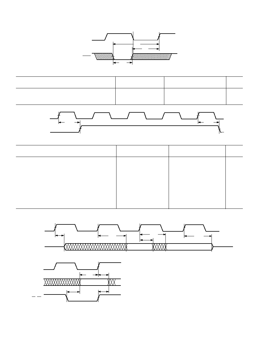
≠20≠
ADSP-21061/ADSP-21061L
REV. B
CLKIN
IRQ2-0
t
IPW
t
SIR
t
HIR
Figure 10. Interrupts
ADSP-21061 (5 V)
ADSP-21061L (3.3 V)
Parameter
Min
Max
Min
Max
Unit
Timer
Switching Characteristics:
t
DTEX
CLKIN High to TIMEXP
15
15
ns
CLKIN
t
DTEX
t
DTEX
TIMEXP
Figure 11. Timer
ADSP-21061 (5 V)
ADSP-21061L (3.3 V)
Parameter
Min
Max
Min
Max
Unit
Timing Requirements:
t
SFI
FLAG3-0
IN
Setup before CLKIN High
1
8 + 5DT/16
8 + 5DT/16
ns
t
HFI
FLAG3-0
IN
Hold after CLKIN High
1
0 ≠ 5DT/16
0 ≠ 5DT/16
ns
t
DWRFI
FLAG3-0
IN
Delay after
RD/WR Low
1
5 + 7DT/16
5 + 7DT/16
ns
t
HFIWR
FLAG3-0
IN
Hold after
RD/WR Deasserted
1
0
0
ns
Switching Characteristics:
t
DFO
FLAG3-0
OUT
Delay after CLKIN High
16
16
ns
t
HFO
FLAG3-0
OUT
Hold after CLKIN High
4
4
ns
t
DFOE
CLKIN High to FLAG3-0
OUT
Enable
3
3
ns
t
DFOD
CLKIN High to FLAG3-0
OUT
Disable
14
14
ns
NOTE
1
Flag inputs meeting these setup and hold times will affect conditional instructions in the following instruction cycle.
CLKIN
FLAG3-0
OUT
FLAG OUTPUT
t
DFO
t
HFO
t
DFO
t
DFOD
t
DFOE
CLKIN
RD, WR
FLAG INPUT
t
SFI
t
HFI
t
HFIWR
t
DWRFI
FLAG3-0
I N
Figure 12. Flags
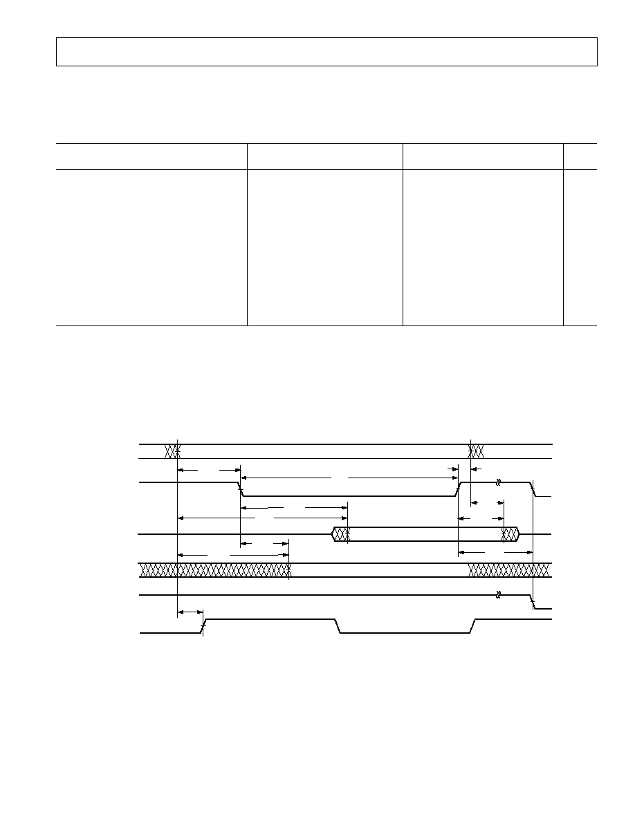
ADSP-21061/ADSP-21061L
≠21≠
REV. B
ADSP-21061 (5 V)
ADSP-21061L (3.3 V)
Parameter
Min
Max
Min
Max
Unit
Timing Requirements:
t
DAD
Address, Selects Delay to Data Valid
1, 2
18 + DT + W
18 + DT + W
ns
t
DRLD
RD Low to Data Valid
1
12 + 5DT/8 + W
12 + 5DT/8 + W
ns
t
HDA
Data Hold from Address, Selects
3
0.5
0.5
ns
t
HDRH
Data Hold from
RD High
3
2.0
2.0
ns
t
DAAK
ACK Delay from Address, Selects
2,
4
15 + 7DT/8 + W
15 + 7DT/8 + W
ns
t
DSAK
ACK Delay from
RD Low
4
8 + DT/2 + W
8 + DT/2 + W
ns
Switching Characteristics:
t
DRHA
Address, Selects Hold after
RD High
0 + H
0 + H
ns
t
DARL
Address, Selects to
RD Low
2
2 + 3DT/8
2 + 3DT/8
ns
t
RW
RD Pulsewidth
12.5 + 5DT/8 + W
12.5 + 5DT/8 + W
ns
t
RWR
RD High to WR, RD, DMAGx Low
8 + 3DT/8 + HI
8 + 3DT/8 + HI
ns
t
SADADC
Address, Selects Setup before
ADRCLK High
2
0 + DT/4
0 + DT/4
ns
W = (number of wait states specified in WAIT register)
◊ t
CK
.
HI = t
CK
(if an address hold cycle or bus idle cycle occurs, as specified in WAIT register; otherwise HI = 0).
H = t
CK
(if an address hold cycle occurs as specified in WAIT register; otherwise H = 0).
NOTES
1
Data Delay/Setup: User must meet t
DAD
or t
DRLD
or synchronous specification t
SSDATI
.
2
The falling edge of
MSx, SW, and BMS is referenced.
3
Data Hold: User must meet t
HDA
or t
HDRH
or synchronous specification t
HSDATI
. See System Hold Time Calculation under Test Conditions for the calculation of hold
times given capacitive and dc loads.
4
ACK Delay/Setup: User must meet t
DAAK
or t
DSAK
or synchronous specification t
SACKC
for deassertion of ACK (Low), all three specifications must be met for asser-
tion of ACK (High).
WR, DMAG
ACK
DATA
RD
ADDRESS
MSx, SW
BMS
t
DARL
t
RW
t
DAD
t
SADADC
t
DAAK
t
HDRH
t
HDA
t
RWR
t
DRLD
ADRCLK
(OUT)
t
DRHA
t
DSAK
Figure 13. Memory Read--Bus Master
Memory Read--Bus Master
Use these specifications for asynchronous interfacing to memo-
ries (and memory-mapped peripherals) without reference to
CLKIN. These specifications apply when the ADSP-21061 is
the bus master accessing external memory space. These switching
characteristics also apply for bus master synchronous read/write
timing (see Synchronous Read/Write--Bus Master). If these
timing requirements are met, the synchronous read/write timing
can be ignored (and vice versa).
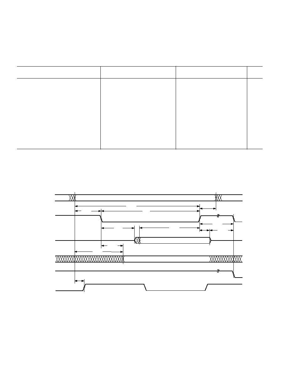
≠22≠
ADSP-21061/ADSP-21061L
REV. B
ADSP-21061 (5 V)
ADSP-21061L (3.3 V)
Parameter
Min
Max
Min
Max
Unit
Timing Requirements:
t
DAAK
ACK Delay from Address, Selects
1, 2
15 + 7DT/8 + W
15 + 7DT/8 + W
ns
t
DSAK
ACK Delay from
WR Low
1
8 + DT/2 + W
8 + DT/2 + W
ns
Switching Characteristics:
t
DAWH
Address, Selects to
WR Deasserted
2
17 + 15DT/16 + W
17 + 15DT/16 + W
ns
t
DAWL
Address, Selects to
WR Low
2
3 + 3DT/8
3 + 3DT/8
ns
t
WW
WR Pulsewidth
13 + 9DT/16 + W
13 + 9DT/16 + W
ns
t
DDWH
Data Setup before
WR High
7 + DT/2 + W
7 + DT/2 + W
ns
t
DWHA
Address Hold after
WR Deasserted
1 + DT/16 + H
0.5 + DT/16 + H
ns
t
DATRWH
Data Disable after
WR Deasserted
3
1 + DT/16 + H
6 + DT/16 + H
1 + DT/16 + H
6 + DT/16 + H
ns
t
WWR
WR High to WR, RD, DMAGx Low
8 + 7DT/16 + H
8 + 7DT/16 + H
ns
t
DDWR
Data Disable before
WR or RD Low
5 + 3DT/8 + I
5 + 3DT/8 + I
ns
t
WDE
WR Low to Data Enabled
≠1 + DT/16
≠1 + DT/16
ns
t
SADADC
Address, Selects to ADRCLK High
2
0 + DT/4
0 + DT/4
ns
W = (number of wait states specified in WAIT register)
◊ t
CK
.
H = t
CK
(if an address hold cycle occurs, as specified in WAIT register; otherwise H = 0).
I = t
CK
(if a bus idle cycle occurs, as specified in WAIT register; otherwise I = 0).
NOTES
1
ACK Delay/Setup: User must meet t
DAAK
or t
DSAK
or synchronous specification t
SACKC
for deassertion of ACK (Low), all three specifications must be met for asser-
tion of ACK (High)
2
The falling edge of
MSx, SW, and BMS is referenced.
3
See System Hold Time Calculation under Test Conditions for calculation of hold times given capacitive and dc loads.
RD, DMAG
ACK
DATA
WR
ADDRESS
MSx , SW
BMS
t
DAWL
t
WW
t
SADADC
t
DAAK
t
WWR
t
WDE
ADRCLK
(OUT)
t
DDWR
t
DATRWH
t
DWHA
t
DDWH
t
DAWH
t
DSAK
Figure 14. Memory Write--Bus Master
Memory Write--Bus Master
Use these specifications for asynchronous interfacing to memo-
ries (and memory-mapped peripherals) without reference to
CLKIN. These specifications apply when the ADSP-21061 is
the bus master accessing external memory space. These switching
characteristics also apply for bus master synchronous read/write
timing (see Synchronous Read/Write--Bus Master). If these
timing requirements are met, the synchronous read/write timing
can be ignored (and vice versa).

ADSP-21061/ADSP-21061L
≠23≠
REV. B
Synchronous Read/Write--Bus Master
Use these specifications for interfacing to external memory
systems that require CLKIN--relative timing or for accessing a
slave ADSP-21061 (in multiprocessor memory space). These
synchronous switching characteristics are also valid during
asynchronous memory reads and writes (see Memory Read--
Bus Master and Memory Write--Bus Master).
When accessing a slave ADSP-2106x, these switching character-
istics must meet the slave's timing requirements for synchronous
read/writes (see Synchronous Read/Write--Bus Slave). The
slave ADSP-21061 must also meet these (bus master) timing
requirements for data and acknowledge setup and hold times.
ADSP-21061 (5 V)
ADSP-21061L (3.3 V)
Parameter
Min
Max
Min
Max
Unit
Timing Requirements:
t
SSDATI
Data Setup before CLKIN
2 + DT/8
2 + DT/8
ns
t
SSDATI
(50 MHz) Data Setup before CLKIN,
t
CK
= 20 ns
1
1.5 + DT/8
ns
t
HSDATI
Data Hold after CLKIN
3.5 ≠ DT/8
3.5 ≠ DT/8
ns
t
DAAK
ACK Delay after Address,
MSx,
SW, BMS
2, 3
15 + 7 DT/8 + W
15 + 7 DT/8 + W
ns
t
SACKC
ACK Setup before CLKIN
2
6.5 + DT/4
6.5 + DT/4
ns
t
HACK
ACK Hold after CLKIN
≠1 ≠ DT/4
≠1 ≠ DT/4
ns
Switching Characteristics:
t
DADRO
Address,
MSx, BMS, SW Delay
after CLKIN
2
6.5 ≠ DT/8
6.5 ≠ DT/8
ns
t
HADRO
Address,
MSx, BMS, SW Hold
after CLKIN
≠1 ≠ DT/8
≠1 ≠ DT/8
ns
t
DPGC
PAGE Delay after CLKIN
9 + DT/8
16 + DT/8
9 + DT/8
16 + DT/8
ns
t
DRDO
RD High Delay after CLKIN
≠1.5 ≠ DT/8
4 ≠ DT/8
≠1.5 ≠ DT/8
4 ≠ DT/8
ns
t
DWRO
WR High Delay after CLKIN
≠2.5 ≠ 3DT/16
4 ≠ 3DT/16
≠2.5 ≠ 3DT/16
4 ≠ 3DT/16
ns
t
DWRO
(50 MHz)
WR High Delay after CLKIN,
t
CK
= 20 ns
1
≠1.5 ≠ 3DT/16
4 ≠ 3DT/16
ns
t
DRWL
RD/WR Low Delay after CLKIN
8 + DT/4
12 + DT/4
8 + DT/4
12 + DT/4
ns
t
SDDATO
Data Delay after CLKIN
19 + 5DT/16
19 + 5DT/16
ns
t
DATTR
Data Disable after CLKIN
4
0 ≠ DT/8
7 ≠ DT/8
0 ≠ DT/8
7 ≠ DT/8
ns
t
DADCCK
ADRCLK Delay after CLKIN
4 + DT/8
10 + DT/8
4 + DT/8
10 + DT/8
ns
t
ADRCK
ADRCLK Period
t
CK
t
CK
ns
t
ADRCKH
ADRCLK Width High
(t
CK
/2 ≠ 2)
(t
CK
/2 ≠ 2)
ns
t
ADRCKL
ADRCLK Width Low
(t
CK
/2 ≠ 2)
(t
CK
/2 ≠ 2)
ns
W = (number of Wait states specified in WAIT register)
◊ t
CK
.
NOTES
1
This specification applies to the ADSP-21061KS-200 (5 V, 50 MHz) operating at t
CK
< 25 ns. For all other devices, use the preceding timing specification of the
same name.
2
ACK Delay/Setup: User must meet t
DAAK
or t
DSAK
or synchronous specification t
SACKC
for deassertion of ACK (Low), all three specifications must be met for assertion
of ACK (High).
3
Data Hold: User must meet t
HDA
or t
HDRH
or synchronous specification t
HDATI
. See System Hold Time Calculation under Test Conditions for the calculation of hold
times given capacitive and dc loads.
4
See System Hold Time Calculation under Test Conditions for calculation of hold times given capacitive and dc loads.
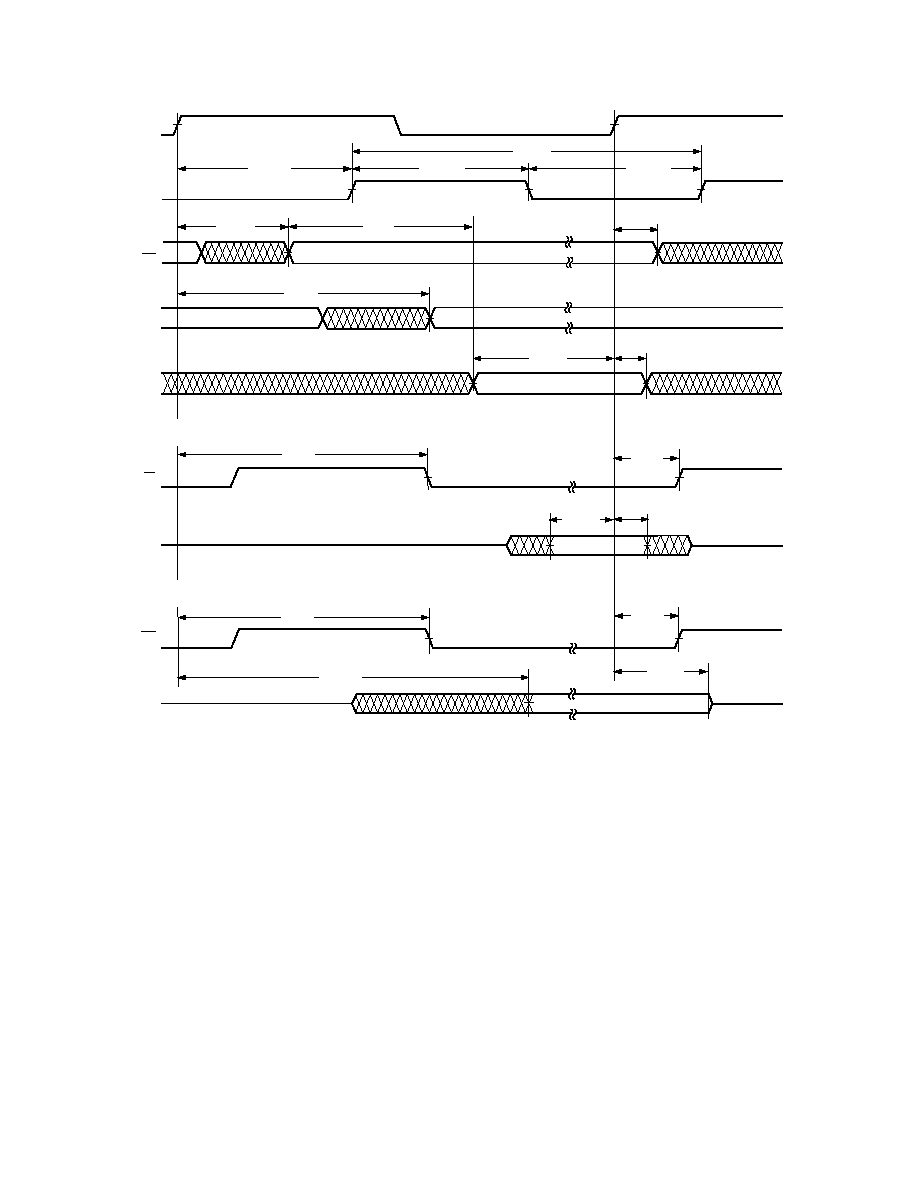
≠24≠
ADSP-21061/ADSP-21061L
REV. B
CLKIN
ADRCLK
ADDRESS
SW
ACK
(IN)
PAGE
RD
DATA
(OUT)
WR
t
DADCCK
t
ADRCK
t
ADRCKL
t
HADRO
t
DAAK
t
DPGC
t
DRWL
t
SACKC
t
HACK
t
HSDATI
t
SSDATI
t
DRDO
t
DWRO
t
DATTR
t
SDDATO
t
DRWL
DATA
(IN)
t
DADRO
t
ADRCKH
WRITE CYCLE
READ CYCLE
Figure 15. Synchronous Read/Write--Bus Master
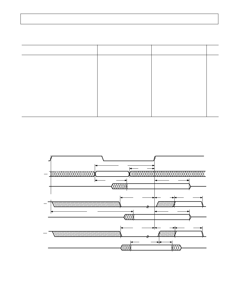
ADSP-21061/ADSP-21061L
≠25≠
REV. B
Synchronous Read/Write --Bus Slave
Use these specifications for ADSP-21061 bus master accesses of
a slave's IOP registers or internal memory (in multiprocessor
memory space). The bus master must meet these (bus slave)
timing requirements.
ADSP-21061 (5 V)
ADSP-21061L (3.3 V)
Parameter
Min
Max
Min
Max
Unit
Timing Requirements:
t
SADRI
Address,
SW Setup before CLKIN
14 + DT/2
14 + DT/2
ns
t
HADRI
Address,
SW Hold before CLKIN
5 + DT/2
5 + DT/2
ns
t
SRWLI
RD/WR Low Setup before CLKIN
1
8.5 + 5DT/16
8.5 + 5DT/16
ns
t
HRWLI
RD/WR Low Hold after CLKIN
≠4 ≠ 5DT/16
8 + 7DT/16
≠4 ≠ 5DT/16
8 + 7DT/16
ns
t
HRWLI
RD/WR Low Hold after CLKIN
44 MHz/50 MHz
2
≠3.5 ≠ 5DT/16
8 + 7DT/16
≠3.5 ≠ 5DT/16
8 + 7DT/16
ns
t
RWHPI
RD/WR Pulse High
3
3
ns
t
SDATWH
Data Setup before
WR High
3
3
ns
t
HDATWH
Data Hold after
WR High
1
1
ns
Switching Characteristics:
t
SDDATO
Data Delay after CLKIN
19 + 5DT/16
19 + 5DT/16
ns
t
DATTR
Data Disable after CLKIN
3
0 ≠ DT/8
7 ≠ DT/8
0 ≠ DT/8
7 ≠ DT/8
ns
t
DACKAD
ACK Delay after Address,
SW
4
8
8
ns
t
ACKTR
ACK Disable after CLKIN
4
≠1 ≠ DT/8
6 ≠ DT/8
≠1 ≠ DT/8
6 ≠ DT/8
ns
NOTES
1
t
SRWLI
(min) = 9.5 + 5DT/16 when Multiprocessor Memory Space Wait State (MMSWS bit in WAIT register) is disabled; when MMSWS is enabled, t
SRWLI
(min)
= 4 + DT/8.
2
This specification applies to the ADSP-21061LKS-176 (3.3 V, 44 MHz) and the ADSP-21061KS-200 (5 V, 50 MHz), o perating at t
CK
<25 ns. For all other devices,
use the preceding timing specification of the same name.
3
See System Hold Time Calculation under Test Conditions for calculation of hold times given capacitive and dc loads.
4
t
DACKAD
is true only if the address and
SW inputs have setup times (before CLKIN) greater than 10 + DT/8 and less than 19 + 3DT/4. If the address and SW inputs have
setup times greater than 19 + 3DT/4, then ACK is valid 15.5 + DT/4 (max) after CLKIN. A slave that sees an address with an M field match will respond with ACK
regardless of the state of MMSWS or strobes. A slave will three-state ACK every cycle with t
ACKTR
.
CLKIN
ADDRESS
SW
ACK
RD
DATA
(OUT)
WR
WRITE ACCESS
t
SADRI
t
HADRI
t
DACKAD
t
ACKTR
t
RWHPI
t
HRWLI
t
SRWLI
t
SDDATO
t
DATTR
t
SRWLI
t
HRWLI
t
RWHPI
t
HDATWH
t
SDATWH
DATA
(IN)
READ ACCESS

≠26≠
ADSP-21061/ADSP-21061L
REV. B
ADSP-21061 (5 V)
ADSP-21061L (3.3 V)
Parameter
Min
Max
Min
Max
Unit
Timing Requirements:
t
HBGRCSV
HBG Low to RD/WR/CS Valid
1
20+ 5DT/4
20 + 5DT/4
ns
t
SHBRI
HBR Setup before CLKIN
2
20 + 3DT/4
20 + 3DT/4
ns
t
HHBRI
HBR Hold before CLKIN
2
14 + 3DT/4
14 + 3DT/4
ns
t
SHBGI
HBG Setup before CLKIN
13 + DT/2
13 + DT/2
ns
t
HHBGI
HBG Hold before CLKIN High
6 + DT/2
6 + DT/2
ns
t
SBRI
BRx, CPA Setup before CLKIN
3
13 + DT/2
13 + DT/2
ns
t
HBRI
BRx, CPA Hold before CLKIN High
6 + DT/2
6 + DT/2
ns
t
SRPBAI
RPBA Setup before CLKIN
20 + 3DT/4
20 + 3DT/4
ns
t
HRPBAI
RPBA Hold before CLKIN
12 + 3DT/4
12 + 3DT/4
ns
Switching Characteristics:
t
DHBGO
HBG Delay after CLKIN
7 ≠ DT/8
7 ≠ DT/8
ns
t
HHBGO
HBG Hold after CLKIN
≠2 ≠ DT/8
≠2 ≠ DT/8
ns
t
DBRO
BRx Delay after CLKIN
5.5 ≠ DT/8
5.5 ≠ DT/8
ns
t
HBRO
BRx Hold after CLKIN
≠2 ≠ DT/8
≠2 ≠ DT/8
ns
t
DCPAO
CPA Low Delay after CLKIN
6.5 ≠ DT/8
8.5 ≠ DT/8
ns
t
TRCPA
CPA Disable after CLKIN
≠2 ≠ DT/8
4.5 ≠ DT/8
≠2 ≠ DT/8
4.5 ≠ DT/8
ns
t
DRDYCS
REDY (O/D) or (A/D) Low from
CS and HBR Low
4
8
12
ns
t
TRDYHG
REDY (O/D) Disable or REDY (A/D)
High from
HBG
4
44 + 27DT/16
40 + 27DT/16
ns
t
ARDYTR
REDY (A/D) Disable from
CS or
HBR High
4
10
10
ns
NOTES
1
For first asynchronous access after
HBR and CS asserted, ADDR
31-0
must be a non-MMS value 1/2 t
CK
before
RD or WR goes low or by t
HBGRCSV
after HBG goes
low. This is easily accomplished by driving an upper address signal high when
HBG is asserted. See the Host Processor Control of the ADSP-2106x section in the
ADSP-2106x SHARC User's Manual, Second Edition.
2
Only required for recognition in the current cycle.
3
CPA assertion must meet the setup to CLKIN; deassertion does not need to meet the setup to CLKIN.
4
(O/D) = open drain, (A/D) = active drive.
Multiprocessor Bus Request and Host Bus Request
Use these specifications for passing of bus mastership between
multiprocessing ADSP-21061s (
BRx) or a host processor
(
HBR, HBG).
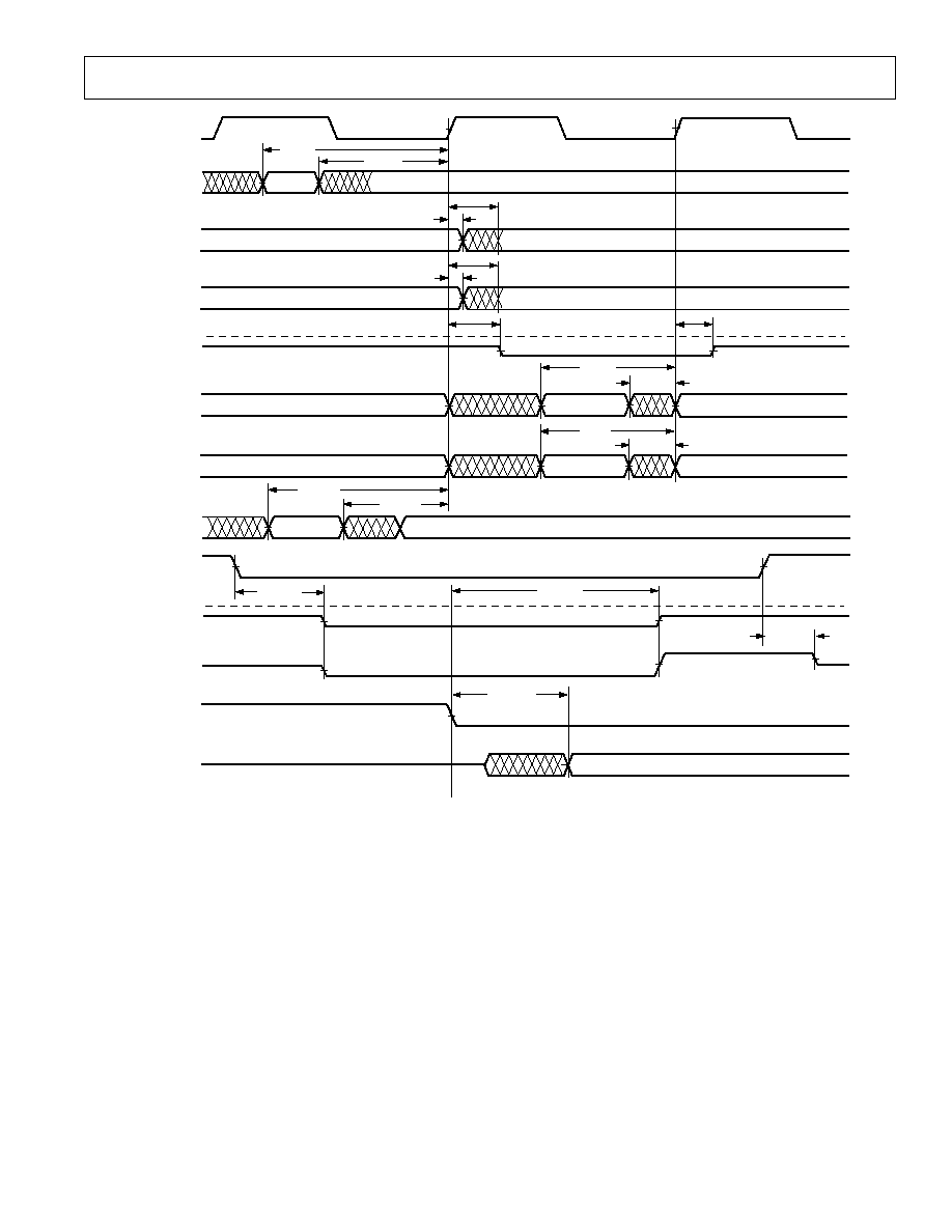
ADSP-21061/ADSP-21061L
≠27≠
REV. B
CLKIN
HBR
HBG
(OUT)
BRx
(OUT)
HBG (IN)
BRx (IN)
HBR
REDY (O/D)
CS
HBG (OUT)
t
DRDYCS
t
HBGRCSV
t
TRDYHG
REDY (A/D)
t
ARDYTR
RD
WR
CS
t
SRPBAI
t
HRPBAI
RPBA
t
SHBRI
t
HHBRI
t
HHBGO
t
DHBGO
t
HBRO
t
DBRO
t
DCPAO
t
TRCPA
t
SHBGI
t
SBRI
CPA (OUT)
(O/D)
CPA (IN) (O/D)
t
HHBGI
t
HBRI
O/D = OPEN DRAIN, A/D = ACTIVE DRIVE
Figure 17. Multiprocessor Bus Request and Host Bus Request
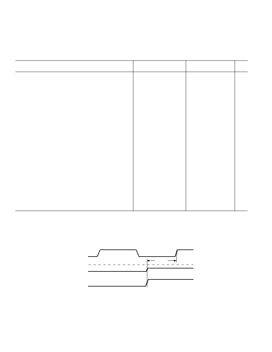
≠28≠
ADSP-21061/ADSP-21061L
REV. B
ADSP-21061 (5 V)
ADSP-21061L (3.3 V)
Parameter
Min
Max
Min
Max
Unit
Read Cycle
Timing Requirements:
t
SADRDL
Address Setup/
CS Low before RD Low
1
0
0
ns
t
HADRDH
Address Hold/
CS Hold Low after RD
0
0
ns
t
WRWH
RD/WR High Width
6
6
ns
t
DRDHRDY
RD High Delay after REDY (O/D) Disable
0
0
ns
t
DRDHRDY
RD High Delay after REDY (A/D) Disable
0
0
ns
Switching Characteristics:
t
SDATRDY
Data Valid before REDY Disable from Low
2
2
ns
t
DRDYRDL
REDY (O/D) or (A/D) Low Delay after
RD Low
10
13.5
ns
t
RDYPRD
REDY (O/D) or (A/D) Low Pulsewidth for Read
45 + DT
45 + DT
ns
t
HDARWH
Data Disable after
RD High
2
8
2
8
ns
Write Cycle
Timing Requirements:
t
SCSWRL
CS Low Setup before WR Low
0
0
ns
t
HCSWRH
CS Low Hold after WR High
0
0
ns
t
SADWRH
Address Setup before
WR High
5
5
ns
t
HADWRH
Address Hold after
WR High
2
2
ns
t
WWRL
WR Low Width
8
8
ns
t
WRWH
RD/WR High Width
6
6
ns
t
DWRHRDY
WR High Delay after REDY (O/D) or (A/D) Disable
0
0
ns
t
SDATWH
Data Setup before
WR High
3
3
ns
t
SDATWH
(50 MHz) Data Setup before
WR High, t
CK
= 20 ns
2
2.5
ns
t
HDATWH
Data Hold after
WR High
1
1
ns
Switching Characteristics:
t
DRDYWRL
REDY (O/D) or (A/D) Low Delay after
WR/CS Low
11
13.5
ns
t
RDYPWR
REDY (O/D) or (A/D) Low Pulsewidth for Write
15
15
ns
t
SRDYCK
REDY (O/D) or (A/D) Disable to CLKIN
1 + 7DT/16
8 + 7DT/16
1 + 7DT/16
8 + 7DT/16
ns
NOTES
1
Not required if
RD and address are valid t
HBGRCSV
after
HBG goes low. For first access after HBR asserted, ADDR
31-0
must be a non-MMS value 1/2 t
CLK
before
RD
or
WR goes low or by t
HBGRCSV
after
HBG goes low. This is easily accomplished by driving an upper address signal high when HBG is asserted. See the Host Proces-
sor Control of the ADSP-2106x section in the ADSP-2106x SHARC User's Manual, Second Edition.
2
This specification applies to the ADSP-21061KS-200 (5 V, 50 MHz) operating at t
CK
< 25 ns. For all other devices, use the preceding timing specification of the
same name.
Asynchronous Read/Write--Host to ADSP-21061
Use these specifications for asynchronous host processor accesses
of an ADSP-21061, after the host has asserted
CS and HBR
(low). After
HBG is returned by the ADSP-21061, the host can
drive the
RD and WR pins to access the ADSP-21061's internal
memory or IOP registers.
HBR and HBG are assumed low for
this timing.
CLKIN
REDY (O/D)
O/D = OPEN DRAIN, A/D = ACTIVE DRIVE
t
SRDYCK
REDY (A/D)
Figure 18a. Synchronous REDY Timing
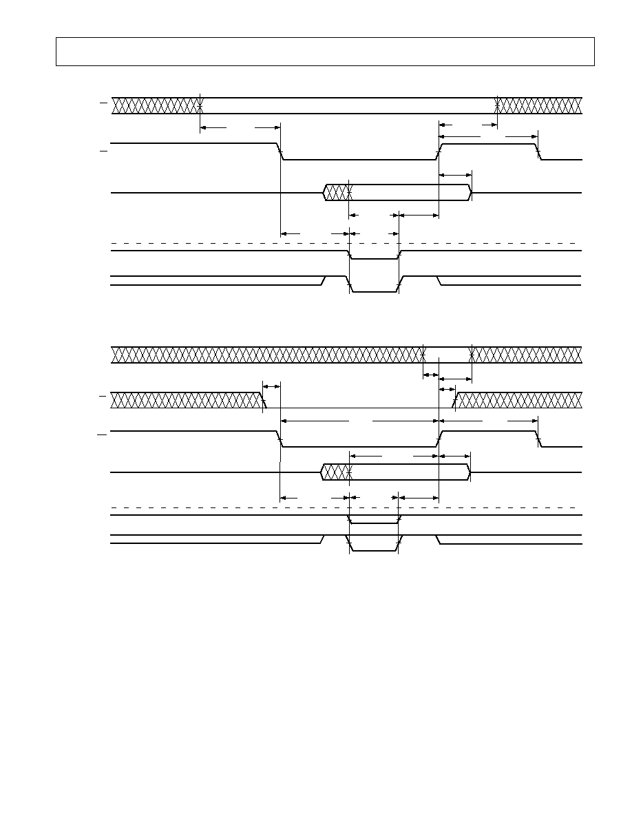
ADSP-21061/ADSP-21061L
≠29≠
REV. B
t
SADRDL
REDY (O/D)
RD
t
DRDYRDL
t
WRWH
t
HADRDH
t
HDARWH
t
RDYPRD
t
DRDHRDY
t
SDATRDY
READ CYCLE
ADDRESS/CS
DATA (OUT)
REDY (A/D)
O/D = OPEN DRAIN, A/D = ACTIVE DRIVE
t
SDATWH
t
HDATWH
t
WWRL
REDY (O/D)
WR
t
DRDYWRL
t
WRWH
t
HADWRH
t
RDYPWR
t
DWRHRDY
WRITE CYCLE
t
SADWRH
DATA (IN)
ADDRESS
REDY (A/D)
t
SCSWRL
CS
t
HCSWRH
Figure 18b. Asynchronous Read/Write--Host to ADSP-2106x

≠30≠
ADSP-21061/ADSP-21061L
REV. B
ADSP-21061 (5 V)
ADSP-21061L (3.3 V)
Parameter
Min
Max
Min
Max
Unit
Timing Requirements:
t
STSCK
SBTS Setup before CLKIN
12 + DT/2
12 + DT/2
ns
t
HTSCK
SBTS Hold before CLKIN
6 + DT/2
6 + DT/2
ns
Switching Characteristics:
t
MIENA
Address/Select Enable after CLKIN
≠1 ≠ DT/8
≠1 ≠ DT/8
ns
t
MIENS
Strobes Enable after CLKIN
1
≠1.5 ≠ DT/8
≠1.5 ≠ DT/8
ns
t
MIENHG
HBG Enable after CLKIN
≠1.5 ≠ DT/8
≠1.5 ≠ DT/8
ns
t
MITRA
Address/Select Disable after CLKIN
0 ≠ DT/4
0 ≠ DT/4
ns
t
MITRS
Strobes Disable after CLKIN
1
1.5 ≠ DT/4
1.5 ≠ DT/4
ns
t
MITRHG
HBG Disable after CLKIN
2 ≠ DT/4
2 ≠ DT/4
ns
t
DATEN
Data Enable after CLKIN
2
9 + 5DT/16
9 + 5DT/16
ns
t
DATTR
Data Disable after CLKIN
2
0 ≠ DT/8
7 ≠ DT/8
0 ≠ DT/8
7 ≠ DT/8
ns
t
ACKEN
ACK Enable after CLKIN
2
7.5 + DT/4
7.5 + DT/4
ns
t
ACKTR
ACK Disable after CLKIN
2
≠1 ≠ DT/8
6 ≠ DT/8
≠1 ≠ DT/8
6 ≠ DT/8
ns
t
ADCEN
ADRCLK Enable after CLKIN
≠2 ≠ DT/8
≠2 ≠ DT/8
ns
t
ADCTR
ADRCLK Disable after CLKIN
8 ≠ DT/4
8 ≠ DT/4
ns
t
MTRHBG
Memory Interface Disable before
HBG Low
3
0 + DT/8
0 + DT/8
ns
t
MENHBG
Memory Interface Enable after
HBG High
3
19 + DT
19 + DT
ns
NOTES
1
Strobes =
RD, WR, MSx, SW, PAGE, DMAG, BMS.
2
In addition to bus master transition cycles, these specifications also apply to bus master and bus slave synchronous read/write.
3
Memory Interface = Address,
RD, WR, MSx, SW, HBG, PAGE, DMAGx, BMS (in EPROM boot mode).
Three-State Timing--Bus Master, Bus Slave,
HBR, SBTS
These specifications show how the memory interface is disabled
(stops driving) or enabled (resumes driving) relative to CLKIN
and the
SBTS pin. This timing is applicable to bus master tran-
sition cycles (BTC) and host transition cycles (HTC) as well as
the
SBTS pin.

ADSP-21061/ADSP-21061L
≠31≠
REV. B
CLKIN
SBTS
ACK
t
MITRA,
t
MITRS,
t
MITRHG
t
STSCK
t
HTSCK
t
DATTR
t
DATEN
t
ACKTR
t
ACKEN
t
ADCTR
t
ADCEN
ADRCLK
DATA
t
MIEN
MEMORY
INTERFACE
Figure 19a. Three-State Timing (Bus Transition Cycle,
SBTS Assertion)
MEMORY
INTERFACE
t
MENHBG
t
MTRHBG
HBG
MEMORY INTERFACE = ADDRESS,
RD, WR, MSx, SW, PAGE, DMAGx. BMS (IN EPROM BOOT MODE)
Figure 19b. Three-State Timing (Host Transition Cycle)

≠32≠
ADSP-21061/ADSP-21061L
REV. B
ADSP-21061 (5 V)
ADSP-21061L (3.3 V)
Parameter
Min
Max
Min
Max
Unit
Timing Requirements:
t
SDRLC
DMARx Low Setup before CLKIN
1
5
5
ns
t
SDRHC
DMARx High Setup before CLKIN
1
5
5
ns
t
WDR
DMARx Width Low (Nonsynchronous)
6
6
ns
t
SDATDGL
Data Setup after
DMAGx Low
2
10 + 5DT/8
10 + 5DT/8
ns
t
HDATIDG
Data Hold after
DMAGx High
2
2
ns
t
DATDRH
Data Valid after
DMARx High
2
16 + 7DT/8
16 + 7DT/8
ns
t
DMARLL
DMAGx Low Edge to Low Edge
23 + 7DT/8
23.5 + 7DT/8
ns
t
DMARH
DMAGx Width High
6
6
ns
Switching Characteristics:
t
DDGL
DMAGx Low Delay after CLKIN
9 + DT/4
15 + DT/4
9 + DT/4
15 + DT/4
ns
t
WDGH
DMAGx High Width
6 + 3DT/8
6 + 3DT/8
ns
t
WDGL
DMAGx Low Width
12 + 5DT/8
12 + 5DT/8
ns
t
HDGC
DMAGx High Delay after CLKIN
≠2 ≠ DT/8
6 ≠ DT/8
≠2 ≠ DT/8
6 ≠ DT/8
ns
t
DADGH
Address Select Valid to
DMAGx High
17 + DT
17 + DT
ns
t
DDGHA
Address Select Hold to
DMAGx High
≠0.5
≠1.0
ns
t
VDATDGH
Data Valid before
DMAGx High
3
8 + 9DT/16
8 + 9DT/16
ns
t
DATRDGH
Data Disable after
DMAGx High
4
0
7
0
7
ns
t
DGWRL
WR Low before DMAGx Low
0
2
0
2
ns
t
DGWRH
DMAGx Low before WR High
10 + 5DT/8 + W
10 + 5DT/8 + W
ns
t
DGWRR
WR High before DMAGx High
1 + DT/16
3 + DT/16
1 + DT/16
3 + DT/16
ns
t
DGRDL
RD Low before DMAGx Low
0
2
0
2
ns
t
DRDGH
RD Low before DMAGx High
11 + 9DT/16 + W
11 + 9DT/16 + W
ns
t
DGRDR
RD High before DMAGx High
0
3
0
3
ns
t
DGWR
DMAGx High to WR, RD, DMAGx Low
5 + 3DT/8 + HI
5 + 3DT/8 + HI
ns
W = (number of wait states specified in WAIT register)
◊ t
CK
.
HI = t
CK
(if an address hold cycle or bus idle cycle occurs, as specified in WAIT register; otherwise HI = 0).
NOTES
1
Only required for recognition in the current cycle.
2
t
SDATDGL
is the data setup requirement if
DMARx is not being used to hold off completion of a write. Otherwise, if DMARx low holds off completion of the write, the
data can be driven t
DATDRH
after
DMARx is brought high.
3
t
VDATDGH
is valid if
DMARx is not being used to hold off completion of a read. If DMARx is used to prolong the read, then t
VDATDGH
= 8 + 9DT/16 + (n
◊ t
CK
) where
n equals the number of extra cycles that the access is prolonged.
4
See System Hold Time Calculation under Test Conditions for calculation of hold times given capacitive and dc loads.
transfer is controlled by ADDR
31-0
,
RD, WR, MS
3-0
and ACK
(not
DMAG). For Paced Master mode, the Memory Read≠Bus
Master, Memory Write≠Bus Master, and Synchronous Read/
Write≠Bus Master timing specifications for ADDR
31-0
,
RD,
WR, MS
3-0
,
SW, PAGE, DATA
47-0
and ACK also apply.
DMA Handshake
These specifications describe the three DMA handshake modes.
In all three modes DMAR is used to initiate transfers. For hand-
shake mode, DMAG controls the latching or enabling of data
externally. For external handshake mode, the data transfer is
controlled by the ADDR
31-0
,
RD, WR, SW, PAGE, MS
3-0
,
ACK and
DMAG signals. For Paced Master mode, the data
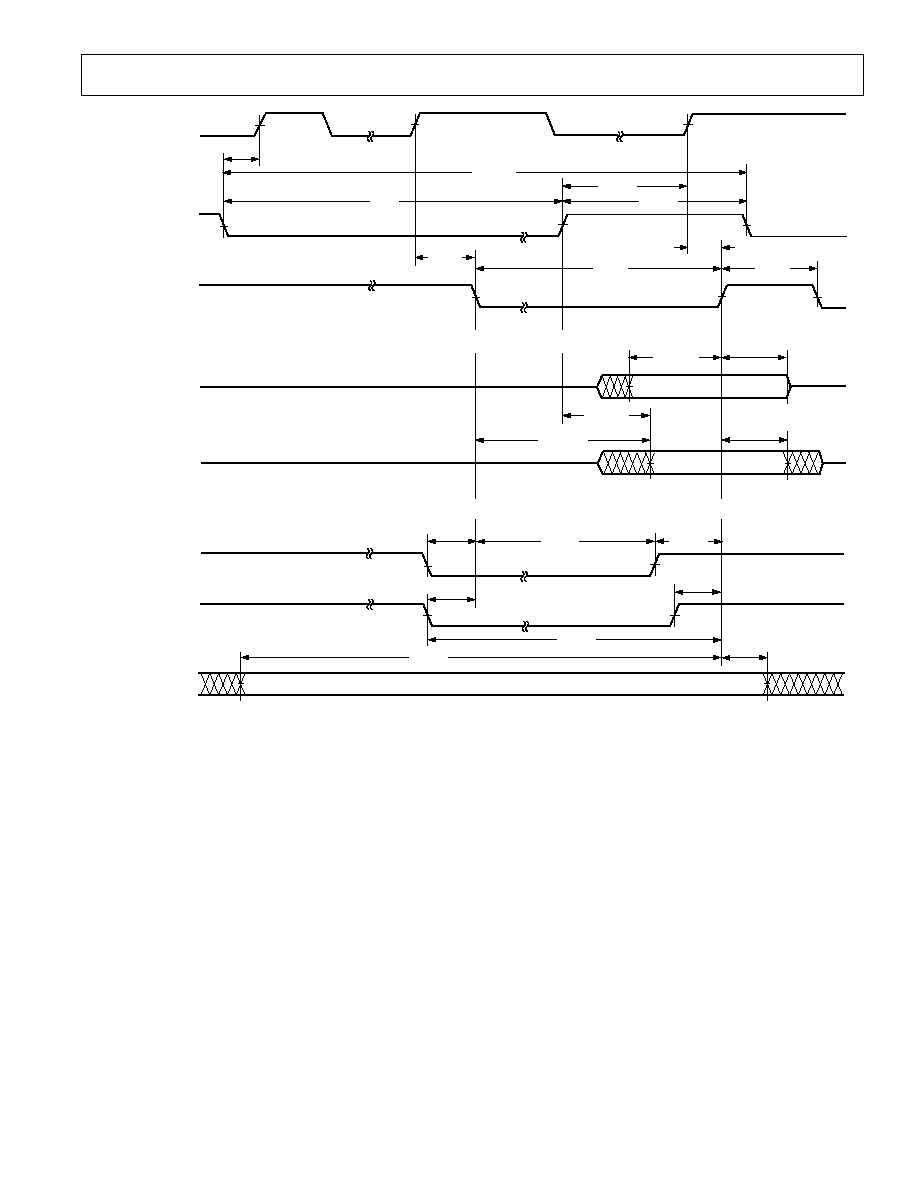
ADSP-21061/ADSP-21061L
≠33≠
REV. B
CLKIN
t
SDRLC
DMARx
DATA (FROM
ADSP-2106x TO
EXTERNAL DRIVE)
DATA (FROM
EXTERNAL DRIVE
TO ADSP-2106x)
RD
(EXTERNAL
MEMORY TO
EXTERNAL DEVICE)
WR
(EXTERNAL DEVICE
TO EXTERNAL
MEMORY)
t
WDR
t
SDRHC
t
DMARH
t
DMARLL
t
HDGC
t
WDGH
t
DDGL
t
WDGL
DMAGx
t
VDATDGH
t
DATDRH
t
DATRDGH
t
HDATIDG
t
DGWRL
t
DGWRH
t
DGWRR
t
DGRDL
t
DRDGH
t
DGRDR
t
SDATDGL
*
"MEMORY READ ≠ BUS MASTER," "MEMORY WRITE ≠ BUS MASTER" AND "SYNCHRONOUS READ/WRITE ≠ BUS MASTER"
TIMING SPECIFICATIONS FOR ADDR
31-0
,
RD, WR, SW, MS
3-0
AND ACK ALSO APPLY HERE.
TRANSFERS BETWEEN ADSP-2106x INTERNAL MEMORY AND EXTERNAL DEVICE
TRANSFERS BETWEEN EXTERNAL DEVICE AND EXTERNAL MEMORY* (EXTERNAL HANDSHAKE MODE)
t
DDGHA
ADDRESS
SW, MSx
t
DADGH
Figure 20. DMA Handshake Timing

≠34≠
ADSP-21061/ADSP-21061L
REV. B
Serial Ports
ADSP-21061 (5 V)
ADSP-21061L (3.3 V)
Parameter
Min
Max
Min
Max
Unit
External Clock
Timing Requirements:
t
SFSE
TFS/RFS Setup before TCLK/RCLK
1
3.5
3.5
ns
t
HFSE
TFS/RFS Hold after TCLK/RCLK
1, 2
4
4
ns
t
SDRE
Receive Data Setup before RCLK
1
1.5
1.5
ns
t
HDRE
Receive Data Hold after RCLK
1
4
4
ns
t
SCLKW
TCLK/RCLK Width
9
9
ns
t
SCLK
TCLK/RCLK Period
t
CK
t
CK
ns
Internal Clock
Timing Requirements:
t
SFSI
TFS Setup before TCLK
1
; RFS Setup before RCLK
1
8
8
ns
t
HFSI
TFS/RFS Hold after TCLK/RCLK
1, 2
1
1
ns
t
SDRI
Receive Data Setup before RCLK
1
3
3
ns
t
HDRI
Receive Data Hold after RCLK
1
3
3
ns
External or Internal Clock
Switching Characteristics:
t
DFSE
RFS Delay after RCLK (Internally Generated RFS)
3
13
13
ns
t
HOFSE
RFS Hold after RCLK (Internally Generated RFS)
3
3
3
ns
External Clock
Switching Characteristics:
t
DFSE
TFS Delay after TCLK (Internally Generated TFS)
3
13
13
ns
t
HOFSE
TFS Hold after TCLK (Internally Generated TFS)
3
3
3
ns
t
DDTE
Transmit Data Delay after TCLK
3
16
16
ns
t
HODTE
Transmit Data Hold after TCLK
3
5
5
ns
Internal Clock
Switching Characteristics:
t
DFSI
TFS Delay after TCLK (Internally Generated TFS)
3
4.5
4.5
ns
t
HOFSI
TFS Hold after TCLK (Internally Generated TFS)
3
≠1.5
≠1.5
ns
t
DDTI
Transmit Data Delay after TCLK
3
7.5
7.5
ns
t
HDTI
Transmit Data Hold after TCLK
3
0
0
ns
t
SCLKIW
TCLK/RCLK Width
(t
SCLK
/2) ≠ 2.5
(t
SCLK
/2) + 2.5
(t
SCLK
/2) ≠ 2.5
(t
SCLK
/2) + 2.5
ns
Enable and Three-State
Switching Characteristics:
t
DDTEN
Data Enable from External TCLK
3
4.5
3.5
ns
t
DDTTE
Data Disable from External TCLK
3
10.5
10.5
ns
t
DDTIN
Data Enable from Internal TCLK
3
0
≠0.5
ns
t
DDTTI
Data Disable from Internal TCLK
3
3
3
ns
t
DCLK
TCLK/RCLK Delay from CLKIN
22 + 3DT/8
22 + 3DT/8
ns
t
DPTR
SPORT Disable after CLKIN
17
17
ns
External Late Frame Sync
Switching Characteristics:
t
DDTLFSE
Data Delay from Late External TFS or
12
12
ns
External RFS with MCE = 1, MFD = 0
4
t
DDTENFS
Data Enable from late FS or MCE = 1, MFD = 0
4
3.5
3.5
ns
To determine whether communication is possible between two devices at clock speed n, the following specifications must be confirmed: 1) frame sync delay and frame
sync setup and hold, 2) data delay and data setup and hold, and 3) SCLK width.
NOTES
1
Referenced to sample edge.
2
RFS hold after RCK when MCE = 1, MFD = 0 is 0 ns minimum from drive edge. TFS hold after TCK for late external. TFS is 0 ns minimum from drive edge.
3
Referenced to drive edge.
4
MCE = 1, TFS enable and TFS valid follow t
DDTLFSE
and t
DDTENFS
.
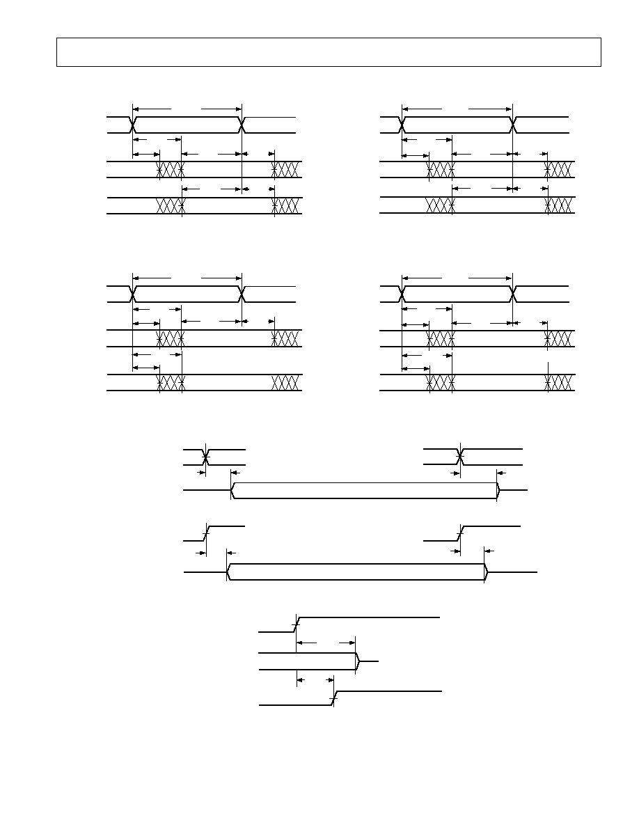
ADSP-21061/ADSP-21061L
≠35≠
REV. B
DT
t
DDTTI
t
DDTIN
DRIVE
EDGE
DRIVE
EDGE
TCLK / RCLK
TCLK (INT)
TFS ("LATE", INT)
DT
t
DDTTE
t
DDTEN
DRIVE
EDGE
DRIVE
EDGE
TCLK / RCLK
TCLK (EXT)
TFS ("LATE" EXT)
t
SDRI
RCLK
RFS
DR
DRIVE
EDGE
SAMPLE
EDGE
t
HDRI
t
SFSI
t
HFSI
t
DFSE
t
HOFSE
t
SCLKIW
DATA RECEIVE≠ INTERNAL CLOCK
t
SDRE
DATA RECEIVE≠ EXTERNAL CLOCK
RCLK
RFS
DR
DRIVE
EDGE
SAMPLE
EDGE
t
HDRE
t
SFSE
t
HFSE
t
DFSE
t
SCLKW
t
HOFSE
NOTE: EITHER THE RISING EDGE OR FALLING EDGE OF RCLK, TCLK CAN BE USED AS THE ACTIVE SAMPLING EDGE.
t
DDTI
t
HDTI
TCLK
TFS
DT
DRIVE
EDGE
SAMPLE
EDGE
t
SFSI
t
HFSI
t
SCLKIW
t
DFSI
t
HOFSI
DATA TRANSMIT≠ INTERNAL CLOCK
t
DDTE
t
HDTE
TCLK
TFS
DT
DRIVE
EDGE
SAMPLE
EDGE
t
SFSE
t
HFSE
t
DFSE
t
SCLKW
t
HOFSE
DATA TRANSMIT≠ EXTERNAL CLOCK
CLKIN
SPORT ENABLE AND
THREE-STATE
LATENCY
IS TWO CYCLES
t
DPTR
t
DCLK
LOW TO HIGH ONLY
TCLK (INT)
RCLK (INT)
TCLK, RCLK
TFS, RFS, DT
NOTE: EITHER THE RISING EDGE OR FALLING EDGE OF RCLK, TCLK CAN BE USED AS THE ACTIVE SAMPLING EDGE.
SPORT DISABLE DELAY
FROM INSTRUCTION
Figure 21. Serial Ports
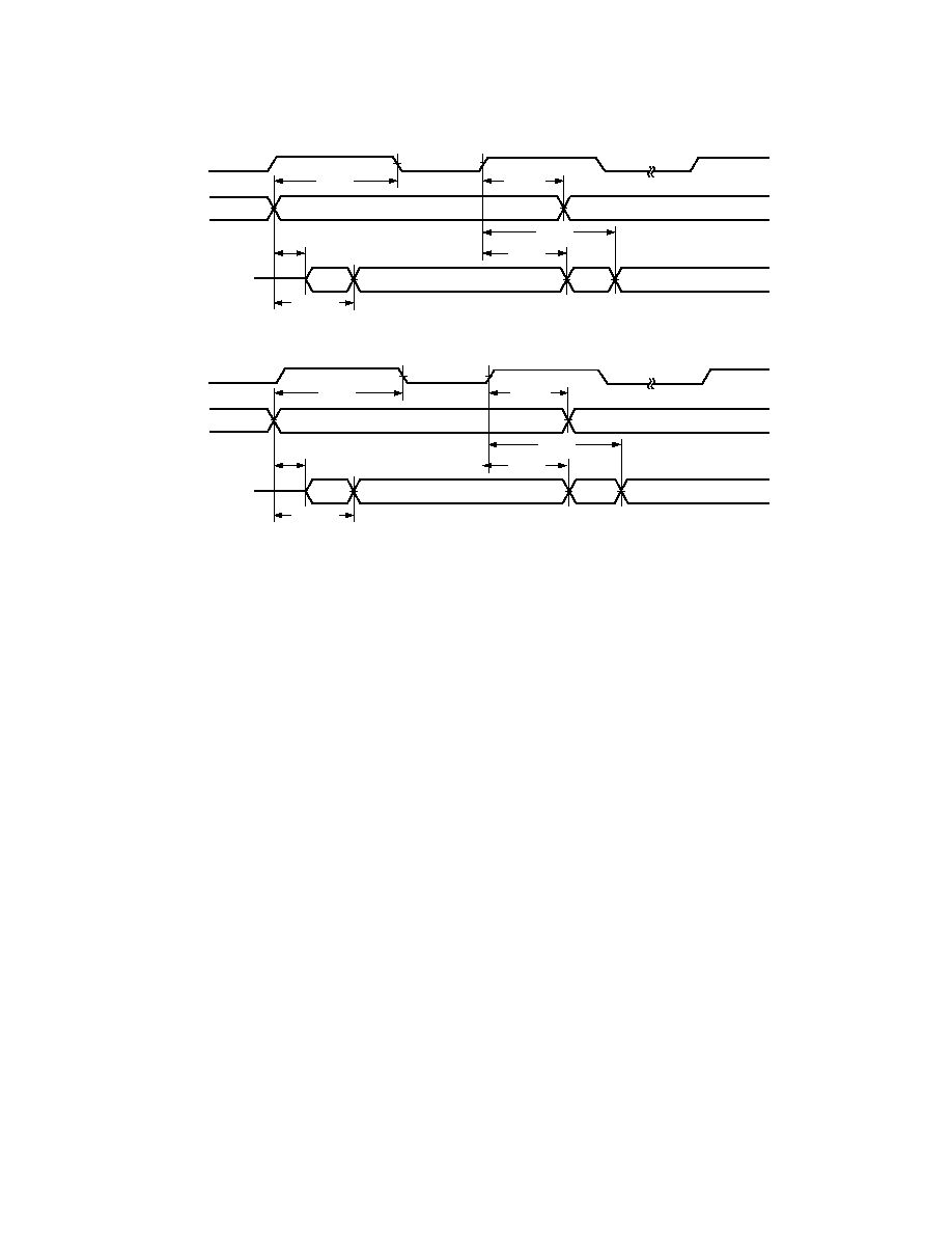
≠36≠
ADSP-21061/ADSP-21061L
REV. B
EXTERNAL RFS WITH MCE = 1, MFD = 0
LATE EXTERNAL TFS
t
HFSE /I
t
SFSE / I
t
DDTENFS
t
DDTE/I
t
HDTE/I
t
DDTLFSE
2ND BIT
DRIVE
SAMPLE
DRIVE
1ST BIT
RCLK
RFS
DT
t
HFSE/I
t
SFSE / I
t
DDTENFS
t
DDTE/I
t
HDTE/I
t
DDTLFSE
2ND BIT
DRIVE
SAMPLE
DRIVE
1ST BIT
TCLK
TFS
DT
*
*
*RFS HOLD AFTER RCK WHEN MCE = 1, MFD = 0 IS 0ns MINIMUM FROM DRIVE EDGE.
TFS HOLD AFTER TCK FOR LATE EXTERNAL. TFS IS 0ns MINIMUM FROM DRIVE EDGE.
Figure 22. External Late Frame Sync
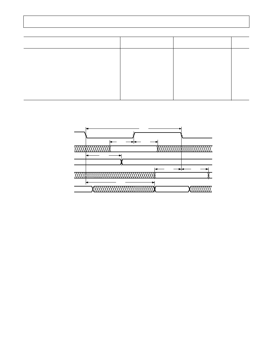
ADSP-21061/ADSP-21061L
≠37≠
REV. B
JTAG Test Access Port and Emulation
ADSP-21061 (5 V)
ADSP-21061L (3.3 V)
Parameter
Min
Max
Min
Max
Unit
Timing Requirements:
t
TCK
TCK Period
t
CK
t
CK
ns
t
STAP
TDI, TMS Setup before TCK High
t
CK
t
CK
ns
t
HTAP
TDI, TMS Hold after TCK High
6
6
ns
t
SSYS
System Inputs Setup before TCK Low
1
7
7
ns
t
HSYS
System Inputs Hold after TCK Low
1
18
18
ns
t
TRSTW
TRST Pulsewidth
4t
CK
4t
CK
ns
Switching Characteristics:
t
DTDO
TDO Delay from TCK Low
13
13
ns
t
DSYS
System Outputs Delay after TCK Low
2
18.5
18.5
ns
NOTES
1
System Inputs = DATA
47-0
, ADDR
31-0
,
RD, WR, ACK, SBTS, SW, HBR, HBG, CS, DMAR1, DMAR2, BR
6-1
, ID
2-0
, RPBA,
IRQ
2-0
, FLAG
3-0
, DR0, DR1,
TCLK0, TCLK1, RCLK0, RCLK1, TFS0, TFS1, RFS0, RFS1, EBOOT, LBOOT,
BMS, CLKIN, RESET.
2
System Outputs = DATA
47-0
, ADDR
31-0
,
MS
3-0
,
RD, WR, ACK, PAGE, ADRCLK, SW, HBG, REDY, DMAG1, DMAG2, BR
6-1
,
CPA, FLAG
3-0
, TIMEXP, DT0,
DT1, TCLK0, TCLK1, RCLK0, RCLK1, TFS0, TFS1, RFS0, RFS1,
BMS.
TCK
t
STAP
t
TCK
t
HTAP
t
DTDO
t
SSYS
t
HSYS
t
DSYS
TMS
TDI
TDO
SYSTEM
INPUTS
SYSTEM
OUTPUTS
Figure 23. JTAG Test Access Port and Emulation
≠38≠
ADSP-21061/ADSP-21061L
REV. B
OUTPUT DRIVE CURRENTS
Figure 27 shows typical I-V characteristics for the output drivers
of the ADSP-2106x. The curves represent the current drive
capability of the output drivers as a function of output voltage.
POWER DISSIPATION
Total power dissipation has two components, one due to inter-
nal circuitry and one due to the switching of external output
drivers. Internal power dissipation is dependent on the instruc-
tion execution sequence and the data operands involved. Inter-
nal power dissipation is calculated in the following way:
P
INT
= I
DDIN
◊ V
DD
The external component of total power dissipation is caused by
the switching of output pins. Its magnitude depends on:
≠ the number of output pins that switch during each cycle (O)
≠ the maximum frequency at which they can switch (f)
≠ their load capacitance (C)
≠ their voltage swing (V
DD
)
and is calculated by:
P
EXT
= O
◊ C ◊ V
DD
2
◊ f
The load capacitance should include the processor's package
capacitance (C
IN
). The switching frequency includes driving the
load high and then back low. Address and data pins can drive
high and low at a maximum rate of 1/(2t
CK
). The write strobe
can switch every cycle at a frequency of 1/t
CK
. Select pins switch
at 1/(2t
CK
), but selects can switch on each cycle.
Example:
Estimate P
EXT
with the following assumptions:
≠A system with one bank of external data memory RAM (32-bit)
≠Four 128K
◊ 8 RAM chips are used, each with a load of 10 pF
≠External data memory writes occur every other cycle, a rate
of 1/(4t
CK
), with 50% of the pins switching
≠The instruction cycle rate is 40 MHz (t
CK
= 25 ns).
The P
EXT
equation is calculated for each class of pins that can
drive:
Table II. External Power Calculations (5 V Device)
Pin
# of
%
Type
Pins
Switching
C
f
V
DD
2
= P
EXT
Address
15
50
◊ 44.7 pF ◊ 10 MHz ◊ 25 V = 0.084 W
MS0
1
0
◊ 44.7 pF ◊ 10 MHz ◊ 25 V = 0.000 W
WR
1
≠
◊ 44.7 pF ◊ 20 MHz ◊ 25 V = 0.022 W
Data
32
50
◊ 14.7 pF ◊ 10 MHz ◊ 25 V = 0.059 W
ADDRCLK
1
≠
◊ 4.7 pF
◊ 20 MHz ◊ 25 V = 0.002 W
P
EXT
= 0.167 W
Table III. External Power Calculations (3.3 V Device)
Pin
# of
%
Type
Pins
Switching
C
f
V
DD
2
= P
EXT
Address
15
50
◊ 44.7 pF ◊ 10 MHz ◊ 10.9 V = 0.037 W
MS0
1
0
◊ 44.7 pF ◊ 10 MHz ◊ 10.9 V = 0.000 W
WR
1
≠
◊ 44.7 pF ◊ 20 MHz ◊ 10.9 V = 0.010 W
Data
32
50
◊ 14.7 pF ◊ 10 MHz ◊ 10.9 V = 0.026 W
ADDRCLK
1
≠
◊ 4.7 pF
◊ 20 MHz ◊ 10.9 V = 0.001 W
P
EXT
= 0.074 W
A typical power consumption can now be calculated for these
conditions by adding a typical internal power dissipation:
P
TOTAL
= P
EXT
+ (I
DDIN2
◊ 5.0 V )
Note that the conditions causing a worst-case P
EXT
are different
from those causing a worst-case P
INT
. Maximum P
INT
cannot
occur while 100% of the output pins are switching from all ones
to all zeros. Note also that it is not common for an application to
have 100% or even 50% of the outputs switching simultaneously.
TEST CONDITIONS
Output Disable Time
Output pins are considered to be disabled when they stop driv-
ing, go into a high impedance state, and start to decay from
their output high or low voltage. The time for the voltage on the
bus to decay by
V is dependent on the capacitive load, C
L
and
the load current, I
L
. This decay time can be approximated by
the following equation:
t
DECAY
=
C
L
V
I
L
The output disable time t
DIS
is the difference between t
MEASURED
and t
DECAY
as shown in Figure 24. The time t
MEASURED
is the
interval from when the reference signal switches to when the
output voltage decays
V from the measured output high or
output low voltage. t
DECAY
is calculated with test loads C
L
and
I
L
, and with
V equal to 0.5 V.
Output Enable Time
Output pins are considered to be enabled when they have made
a transition from a high impedance state to when they start
driving. The output enable time t
ENA
is the interval from when a
reference signal reaches a high or low voltage level to when the
output has reached a specified high or low trip point, as shown
in the Output Enable/Disable diagram (Figure 24). If multiple
pins (such as the data bus) are enabled, the measurement value
is that of the first pin to start driving.
ADSP-21061/ADSP-21061L
≠39≠
REV. B
Example System Hold Time Calculation
To determine the data output hold time in a particular system,
first calculate t
DECAY
using the equation given above. Choose
V
to be the difference between the ADSP-2106x's output voltage
and the input threshold for the device requiring the hold time. A
typical
V will be 0.4 V. C
L
is the total bus capacitance (per
data line), and I
L
is the total leakage or three-state current (per
data line). The hold time will be t
DECAY
plus the minimum
disable time (i.e., t
DATRWH
for the write cycle).
REFERENCE
SIGNAL
t
DIS
OUTPUT STARTS
DRIVING
V
OH (MEASURED)
≠ V
V
OL (MEASURED)
+ V
t
MEASURED
V
OH (MEASURED)
V
OL (MEASURED)
2.0V
1.0V
V
OH (MEASURED)
V
OL (MEASURED)
HIGH-IMPEDANCE STATE.
TEST CONDITIONS CAUSE
THIS VOLTAGE TO BE
APPROXIMATELY 1.5V
OUTPUT STOPS
DRIVING
t
ENA
t
DECAY
OUTPUT
Figure 24. Output Enable/Disable
+1.5V
50pF
TO
OUTPUT
PIN
I
OL
I
OH
Figure 25. Equivalent Device Loading for AC Measure-
ments (Includes All Fixtures)
Capacitive Loading
Output delays and holds are based on standard capacitive loads:
50 pF on all pins (see Figure 25). The delay and hold specifica-
tions given should be derated by a factor of 1.5 ns/50 pF for
loads other than the nominal value of 50 pF. Figures 28≠29,
32≠33 show how output rise time varies with capacitance. Fig-
ures 30, 34 show graphically how output delays and holds vary
with load capacitance. (Note that this graph or derating does
not apply to output disable delays; see the previous section
Output Disable Time under Test Conditions.) The graphs of
Figures 28, 29 and 30 may not be linear outside the ranges
shown.
INPUT OR
OUTPUT
1.5V
1.5V
Figure 26. Voltage Reference Levels for AC Measure-
ments (Except Output Enable/Disable)
≠40≠
ADSP-21061/ADSP-21061L
REV. B
SOURCE VOLTAGE ≠ V
100
≠75
≠150
0
5.25
SOURCE CURRENT
≠
mA
0.75
1.50
2.25
3.00
3.75
4.50
75
≠50
≠100
≠125
25
≠25
50
0
≠175
≠200
4.75V, +85 C
5.0V, +25 C
5.25V, ≠40 C
4.75V, +85 C
5.0V, +25 C
5.25V, ≠40 C
Figure 27. ADSP-2106x Typical Drive Currents (V
DD
= 5 V)
LOAD CAPACITANCE ≠ pF
16.0
8.0
0
0
200
20
40
60
80
100
120
140
160
180
14.0
12.0
4.0
2.0
10.0
6.0
FALL TIME
RISE TIME
RISE AND FALL TIMES
≠
ns
(0.5V
≠
4.5V, 10%
≠
90%)
Y = 0.005X + 3.7
Y = 0.0031X + 1.1
Figure 28. Typical Output Rise Time (10%≠90% V
DD
) vs.
Load Capacitance (V
DD
= 5 V)
3.5
0
RISE AND FALL TIMES
≠
ns (0.8V
≠
2.0V)
3.0
2.5
2.0
1.5
1.0
0.5
LOAD CAPACITANCE ≠ pF
0
200
20
40
60
80
100
120
140
160
180
FALL TIME
RISE TIME
Y = 0.009X + 1.1
Y = 0.005X + 0.6
Figure 29. Typical Output Rise Time (0.8 V≠2.0 V) vs.
Load Capacitance (V
DD
= 5 V)
LOAD CAPACITANCE ≠ pF
OUTPUT DELAY OR HOLD
≠
ns
5
≠1
25
200
50
75
100
125
150
175
4
3
2
1
NOMINAL
Y = 0.03X ≠1.45
Figure 30. Typical Output Delay or Hold vs. Load Capaci-
tance (at Maximum Case Temperature) (V
DD
= 5 V)
SOURCE VOLTAGE ≠ Volts
≠120
0
3.6
0.5
SOURCE CURRENT
≠
mA
1
1.5
2
2.5
3
60
≠40
≠60
≠80
≠100
20
≠20
40
0
120
80
100
3.0V +85 C
3.3V +25 C
3.6V ≠40 C
V
OH
3.0V +85 C
3.3V +25 C
3.6V ≠40 C
V
OL
Figure 31. ADSP-2106x Typical Drive Currents (V
DD
= 3.3 V)
LOAD CAPACITANCE ≠ pF
0
2
0
20
40
60
80
100
120
Y = 0.0796X + 1.17
Y = 0.0467X + 0.55
RISE TIME
FALL TIME
140
160
180
200
4
6
8
10
12
14
16
18
RISE AND FALL TIMES
≠
ns (10%
≠
90%)
Figure 32. Typical Output Rise Time (10%≠90% V
DD
) vs.
Load Capacitance (V
DD
= 3.3 V)
ADSP-21061/ADSP-21061L
≠41≠
REV. B
ENVIRONMENTAL CONDITIONS
Thermal Characteristics
The ADSP-21061KS (5 V) device is packaged in a 240-lead
thermally enhanced MQFP. The top surface of the package
contains a copper slug from which most of the die heat is dissi-
pated. The slug is flush with the top surface of the package.
Note that the copper slug is internally connected to GND
through the device substrate. The ADSP-21061LKS is packaged
in a 240-lead MQFP without a copper heat slug. The ADSP-
21061L is also available in a 225-Ball PBGA package. The
PBGA has a
JC
of 1.7
∞C/W. The ADSP-2106x is specified for a
case temperature (T
CASE
). To ensure that the T
CASE
data sheet
specification is not exceeded, a heatsink and/or an air flow
source may be used. A heatsink should be attached with a ther-
mal adhesive.
T
CASE
=
T
AMB
+
( PD
◊
CA
)
T
CASE
= Case temperature (measured on top surface of package)
PD =
Power dissipation in W (this value depends upon the
specific application; a method for calculating PD is
shown under Power Dissipation).
CA
=
Value from tables below.
ADSP-21061 (5 V MQFP Package)
JC
= 0.3 C/W
Airflow
(Linear Ft./Min.)
0
100
200
400
600
CA
(
∞C/W)
10
9
8
7
6
NOTES
This represents thermal resistance at total power of 5 W.
With air flow, no variance is seen in
CA
with power.
CA
at 0 LFM varies with power: at 2W,
CA
= 14
∞C/W, at 3W
CA
= 11
∞C/W.
ADSP-21061L (3.3 V MQFP Package)
JC
= 6.3 C/W
Airflow
(Linear Ft./Min.)
0
100
200
400
600
CA
(
∞C/W)
19.6
17.6
15.6
13.9
12.2
NOTE
With air flow, no variance is seen in
CA
with power.
ADSP-21061L (3.3 V PBGA Package)
JC
= 1.7 C/W
Airflow
(Linear Ft./Min.)
0
200
400
CA
(
∞C/W)
19.0
13.6
11.2
NOTE
With air flow, no variance is seen in
CA
with power.
LOAD CAPACITANCE ≠ pF
0
0
20
40
60
80
100
120
Y = 0.0391X + 0.36
Y = 0.0305X + 0.24
RISE TIME
FALL TIME
140
160
180
200
RISE AND FALL TIMES
≠
ns (0.8V
≠
2.0V)
1
2
3
4
5
6
7
8
9
Figure 33. Typical Output Rise Time (0.8 V≠2.0 V) vs.
Load Capacitance (V
DD
= 3.3 V)
LOAD CAPACITANCE ≠ pF
OUTPUT DELAY OR HOLD
≠
ns
5
≠1
25
200
50
75
100
125
150
175
4
3
2
1
NOMINAL
Y = 0.0329X ≠1.65
Figure 34. Typical Output Delay or Hold vs. Load Capaci-
tance (at Maximum Case Temperature) (V
DD
= 3.3 V)
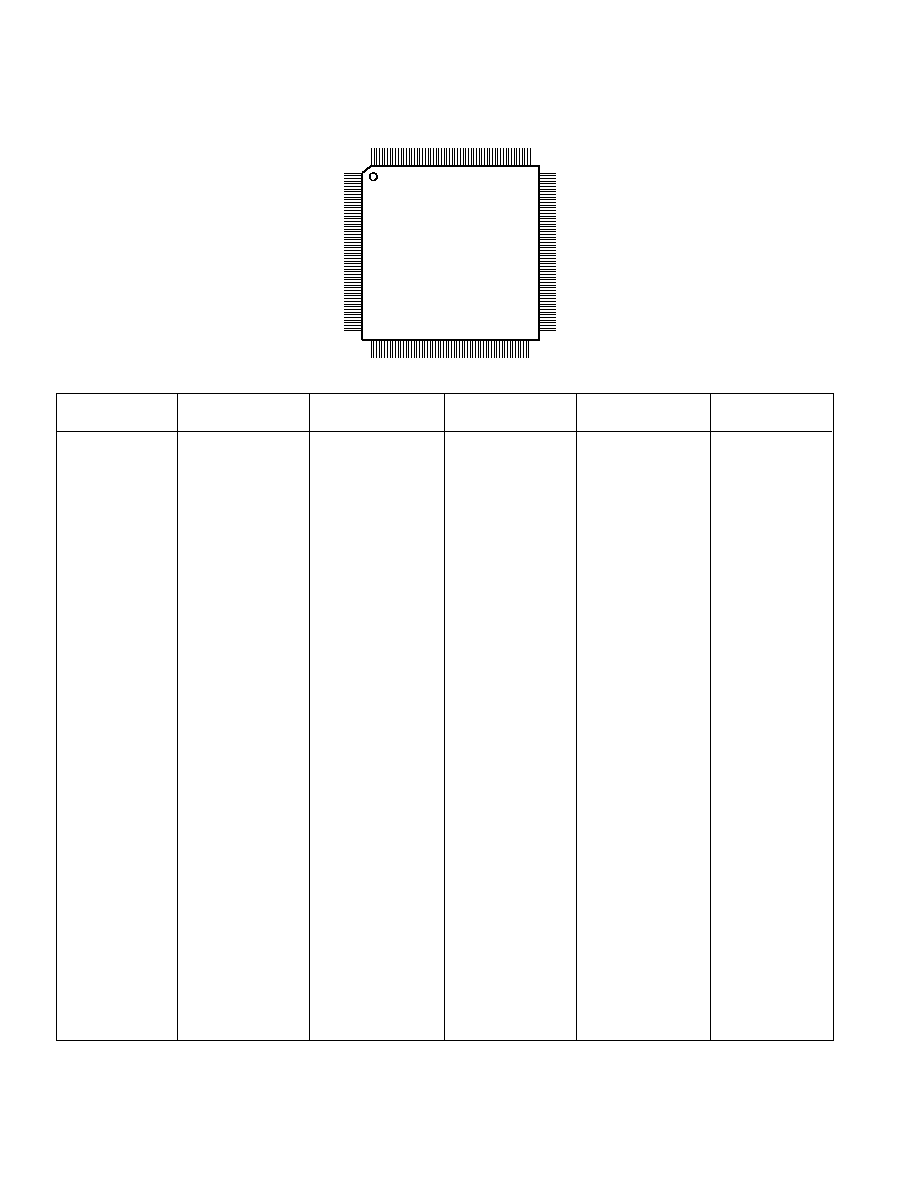
≠42≠
ADSP-21061/ADSP-21061L
REV. B
240-LEAD METRIC MQFP PIN CONFIGURATIONS
1
240
60
61
120
121
180
181
TOP VIEW
Pin
Pin
No.
Name
1
TDI
2
TRST
3
VDD
4
TDO
5
TIMEXP
6
EMU
7
ICSA
8
FLAG3
9
FLAG2
10
FLAG1
11
FLAG0
12
GND
13
ADDR0
14
ADDR1
15
VDD
16
ADDR2
17
ADDR3
18
ADDR4
19
GND
20
ADDR5
21
ADDR6
22
ADDR7
23
VDD
24
ADDR8
25
ADDR9
26
ADDR10
27
GND
28
ADDR11
29
ADDR12
30
ADDR13
31
VDD
32
ADDR14
33
ADDR15
34
GND
35
ADDR16
36
ADDR17
37
ADDR18
38
VDD
39
VDD
40
ADDR19
Pin
Pin
No.
Name
121
DATA41
122
DATA40
123
DATA39
124
VDD
125
DATA38
126
DATA37
127
DATA36
128
GND
129
NC
130
DATA35
131
DATA34
132
DATA33
133
VDD
134
VDD
135
GND
136
DATA32
137
DATA31
138
DATA30
139
GND
140
DATA29
141
DATA28
142
DATA27
143
VDD
144
VDD
145
DATA26
146
DATA25
147
DATA24
148
GND
149
DATA23
150
DATA22
151
DATA21
152
VDD
153
DATA20
154
DATA19
155
DATA18
156
GND
157
DATA17
158
DATA16
159
DATA15
160
VDD
Pin
Pin
No.
Name
81
TCLK0
82
TFS0
83
DR0
84
RCLK0
85
RFS0
86
VDD
87
VDD
88
GND
89
ADRCLK
90
REDY
91
HBG
92
CS
93
RD
94
WR
95
GND
96
VDD
97
GND
98
CLKIN
99
ACK
100
DMAG2
101
DMAG1
102
PAGE
103
VDD
104
BR6
105
BR5
106
BR4
107
BR3
108
BR2
109
BR1
110
GND
111
VDD
112
GND
113
DATA47
114
DATA46
115
DATA45
116
VDD
117
DATA44
118
DATA43
119
DATA42
120
GND
Pin Pin
No. Name
201 NC
202 NC
203 NC
204 NC
205 VDD
206 NC
207 NC
208 NC
209 NC
210 NC
211 NC
212 GND
213 NC
214 NC
215 NC
216 NC
217 NC
218 NC
219 VDD
220 GND
221 VDD
222 NC
223 NC
224 NC
225 NC
226 NC
227 NC
228 GND
229 ID2
230 ID1
231 ID0
232 LBOOT
233 RPBA
234
RESET
235 EBOOT
236
IRQ2
237
IRQ1
238
IRQ0
239 TCK
240 TMS
Pin
Pin
No.
Name
161
DATA14
162
DATA13
163
DATA12
164
GND
165
DATA11
166
DATA10
167
DATA9
168
VDD
169
DATA8
170
DATA7
171
DATA6
172
GND
173
DATA5
174
DATA4
175
DATA3
176
VDD
177
DATA2
178
DATA1
179
DATA0
180
GND
181
GND
182
NC
183
NC
184
NC
185
NC
186
NC
187
NC
188
VDD
189
NC
190
NC
191
NC
192
NC
193
NC
194
NC
195
GND
196
GND
197
VDD
198
NC
199
NC
200
NC
Pin
Pin
No.
Name
41
ADDR20
42
ADDR21
43
GND
44
ADDR22
45
ADDR23
46
ADDR24
47
VDD
48
GND
49
VDD
50
ADDR25
51
ADDR26
52
ADDR27
53
GND
54
MS3
55
MS2
56
MS1
57
MS0
58
SW
59
BMS
60
ADDR28
61
GND
62
VDD
63
VDD
64
ADDR29
65
ADDR30
66
ADDR31
67
GND
68
SBTS
69
DMAR2
70
DMAR1
71
HBR
72
DT1
73
TCLK1
74
TFS1
75
DR1
76
RCLK1
77
RFS1
78
GND
79
CPA
80
DT0
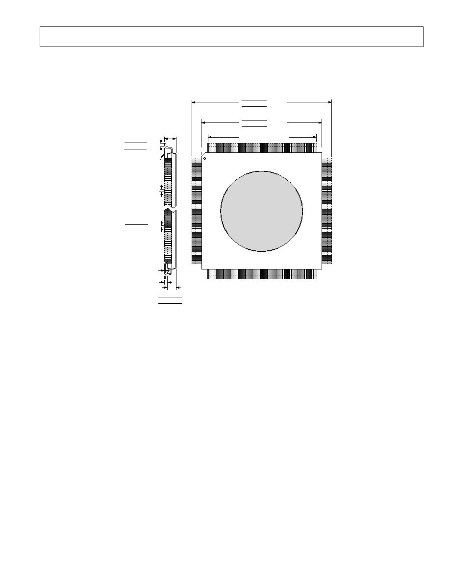
ADSP-21061/ADSP-21061L
≠43≠
REV. B
OUTLINE DIMENSIONS
Dimensions shown in inches and (mm).
240-Lead Metric Thermally Enhanced MQFP (5 V Device Only)
1
181
180
121
120
61
60
GND
HEAT
SLUG
240 LEAD METRIC MQFP
TOP VIEW (PINS DOWN)
INCHES (MILLIMETERS)
240
1.372 (34.85)
1.362 (34.60) TYP SQ
1.352 (34.35)
1.264 (32.10)
1.260 (32.00) TYP SQ
1.256 (31.90)
1.161 (29.50) BSC SQ
THE THERMALLY ENHANCED MQFP PACKAGE CONTAINS A
COPPER HEAT SLUG FLUSH WITH ITS TOP SURFACE; THE
SLUG IS EITHER CONNECTED TO GROUND OR FLOATING.
THE HEAT SLUG DIAMETER IS 24.1 (0.949) mm.
SEATING
PLANE
0.161 (4.10)
MAX
0.030 (0.75)
0.024 (0.60) TYP
0.020 (0.50)
0.003 (0.08)
MAX
0.010 (0.25)
MIN
0.011 (0.27)
0.009 (0.22) TYP
0.007 (0.17)
LEAD PITCH
0.01969 (0.50)
TYP
LEAD WIDTH
0.138 (3.50)
0.134 (3.40) TYP
0.130 (3.30)
NOTE:
THE ACTUAL POSITION OF EACH LEAD IS WITHIN (0.08)
0.0032 FROM ITS IDEAL POSITION WHEN MEASURED IN THE
LATERAL DIRECTION.
CENTER FIGURES ARE TYPICAL UNLESS OTHERWISE NOTED.
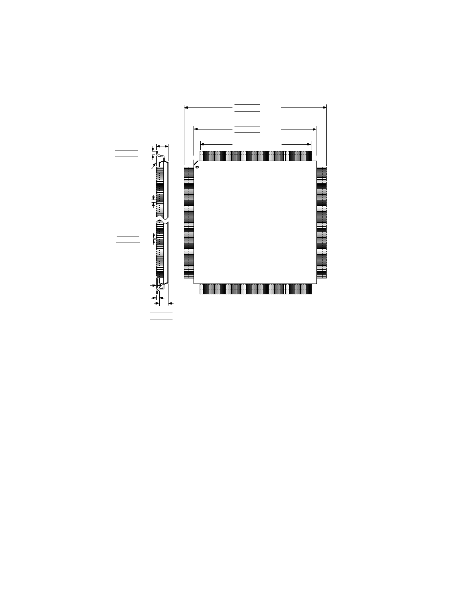
≠44≠
ADSP-21061/ADSP-21061L
REV. B
OUTLINE DIMENSIONS
Dimensions shown in inches and (mm).
240-Lead Metric MQFP (3.3 V Device Only)
1
181
180
121
120
61
60
240 LEAD METRIC MQFP
TOP VIEW (PINS DOWN)
240
INCHES (MILLIMETERS)
1.372 (34.85)
1.362 (34.60) TYP SQ
1.352 (34.35)
1.264 (32.10)
1.260 (32.00) TYP SQ
1.256 (31.90)
1.161 (29.50) BSC SQ
SEATING
PLANE
0.161 (4.10)
MAX
0.030 (0.75)
0.024 (0.60) TYP
0.020 (0.50)
0.003 (0.08)
MAX
0.010 (0.25)
MIN
0.138 (3.50)
0.134 (3.40) TYP
0.130 (3.30)
0.011 (0.27)
0.009 (0.22) TYP
0.007 (0.17)
LEAD PITCH
0.01969 (0.50)
TYP
LEAD WIDTH
NOTE:
THE ACTUAL POSITION OF EACH LEAD IS WITHIN (0.08)
0.0032 FROM ITS IDEAL POSITION WHEN MEASURED IN THE
LATERAL DIRECTION.
CENTER FIGURES ARE TYPICAL UNLESS OTHERWISE NOTED.

ADSP-21061/ADSP-21061L
≠45≠
REV. B
ADSP-21061L 225-Ball Plastic Ball Grid Array (PBGA) Package Pinout
Ball #
Name
Ball #
Name
Ball #
Name
Ball #
Name
Ball #
Name
A01
BMS
D01
ADDR25
G01
ADDR14
K01
ADDR6
N01
EMU
A02
ADDR30
D02
ADDR26
G02
ADDR15
K02
ADDR5
N02
TDO
A03
DMAR2
D03
MS2
G03
ADDR16
K03
ADDR3
N03
IRQ0
A04
DT1
D04
ADDR29
G04
ADDR19
K04
ADDR0
N04
IRQ1
A05
RCLK1
D05
DMAR1
G05
GND
K05
ICSA
N05
ID2
A06
TCLK0
D06
TFS1
G06
VDD
K06
GND
N06
NC
A07
RCLK0
D07
CPA
G07
VDD
K07
VDD
N07
NC
A08
ADRCLK
D08
HBG
G08
VDD
K08
VDD
N08
NC
A09
CS
D09
DMAG2
G09
VDD
K09
VDD
N09
NC
A10
CLKIN
D10
BR5
G10
VDD
K10
GND
N10
NC
A11
PAGE
D11
BR1
G11
GND
K11
GND
N11
NC
A12
BR3
D12
DATA40
G12
DATA22
K12
DATA8
N12
NC
A13
DATA47
D13
DATA37
G13
DATA25
K13
DATA11
N13
NC
A14
DATA44
D14
DATA35
G14
DATA24
K14
DATA13
N14
DATA1
A15
DATA42
D15
DATA34
G15
DATA23
K15
DATA14
N15
DATA3
B01
MS0
E01
ADDR21
H01
ADDR12
L01
ADDR2
P01
TRST
B02
SW
E02
ADDR22
H02
ADDR11
L02
ADDR1
P02
TMS
B03
ADDR31
E03
ADDR24
H03
ADDR13
L03
FLAG0
P03
EBOOT
B04
HBR
E04
ADDR27
H04
ADDR10
L04
FLAG3
P04
ID0
B05
DR1
E05
GND
H05
GND
L05
RPBA
P05
NC
B06
DT0
E06
GND
H06
VDD
L06
GND
P06
NC
B07
DR0
E07
GND
H07
VDD
L07
GND
P07
NC
B08
REDY
E08
GND
H08
VDD
L08
GND
P08
NC
B09
RD
E09
GND
H09
VDD
L09
GND
P09
NC
B10
ACK
E10
GND
H10
VDD
L10
GND
P10
NC
B11
BR6
E11
NC
H11
GND
L11
NC
P11
NC
B12
BR2
E12
DATA33
H12
DATA18
L12
DATA4
P12
NC
B13
DATA45
E13
DATA30
H13
DATA19
L13
DATA7
P13
NC
B14
DATA43
E14
DATA32
H14
DATA21
L14
DATA9
P14
NC
B15
DATA39
E15
DATA31
H15
DATA20
L15
DATA10
P15
DATA0
C01
MS3
F01
ADDR17
J01
ADDR9
M01
FLAG1
R01
TCK
C02
MS1
F02
ADDR18
J02
ADDR8
M02
FLAG2
R02
IRQ2
C03
ADDR28
F03
ADDR20
J03
ADDR7
M03
TIMEXP
R03
RESET
C04
SBTS
F04
ADDR23
J04
ADDR4
M04
TDI
R04
ID1
C05
TCLK1
F05
GND
J05
GND
M05
GND
R05
NC
C06
RFS1
F06
GND
J06
VDD
M06
NC
R06
NC
C07
TFS0
F07
VDD
J07
VDD
M07
NC
R07
NC
C08
RFS0
F08
VDD
J08
VDD
M08
NC
R08
NC
C09
WR
F09
VDD
J09
VDD
M09
NC
R09
NC
C10
DMAG1
F10
GND
J10
VDD
M10
NC
R10
NC
C11
BR4
F11
GND
J11
GND
M11
NC
R11
NC
C12
DATA46
F12
DATA29
J12
DATA12
M12
NC
R12
NC
C13
DATA41
F13
DATA26
J13
DATA15
M13
DATA2
R13
NC
C14
DATA38
F14
DATA28
J14
DATA16
M14
DATA5
R14
NC
C15
DATA36
F15
DATA27
J15
DATA17
M15
DATA6
R15
NC

≠46≠
ADSP-21061/ADSP-21061L
REV. B
225-Ball Plastic Ball Grid Array (PBGA) Package Pinout
Bottom View
15
14
13
12
11
10
9
8
7
6
5
4
3
2
1
A
B
C
D
E
F
G
H
J
K
L
M
N
P
R
ADRCLK
BMS
ADDR30
DMAR2
DT1
RCLK1
TCLK0
RCLK0
CS
CLKIN
PAGE
BR3
DATA47
DATA44
DATA42
MS0
SW
ADDR31
HBR
DR1
DT0
DR0
REDY
RD
ACK
BR6
BR2
DATA45
DATA43
DATA39
MS3
MS1
ADDR28
SBTS
TCLK1
RFS1
TFS0
RFS0
WR
DMAG1
BR4
DATA46
DATA41
DATA38
DATA36
ADDR25
ADDR26
MS2
ADDR29
DMAR1
TFS1
CPA
HBG
DMAG2
BR5
BR1
DATA40
DATA37
DATA35
DATA34
ADDR21
ADDR22
ADDR24
ADDR27
GND
GND
GND
GND
GND
GND
NC
DATA33
DATA30
DATA32
DATA31
ADDR17
ADDR18
ADDR20
ADDR23
GND
GND
VDD
VDD
VDD
GND
GND
DATA29
DATA26
DATA28
DATA27
ADDR14
ADDR15
ADDR16
ADDR19
GND
VDD
VDD
VDD
VDD
VDD
GND
DATA22
DATA25
DATA24
DATA23
ADDR12
ADDR11
ADDR13
ADDR10
GND
VDD
VDD
VDD
VDD
VDD
GND
DATA18
DATA19
DATA21
DATA20
ADDR9
ADDR8
ADDR7
ADDR4
GND
VDD
VDD
VDD
VDD
VDD
GND
DATA12
DATA15
DATA16
DATA17
ADDR6
ADDR5
ADDR3
ADDR0
ICSA
GND
VDD
VDD
VDD
GND
GND
DATA8
DATA11
DATA13
DATA14
ADDR2
ADDR1
FLAG0
FLAG3
RPBA
GND
GND
GND
GND
GND
NC
DATA4
DATA7
DATA9
DATA10
FLAG1
FLAG2
TIMEXP
TDI
GND
NC
NC
NC
NC
NC
NC
NC
DATA2
DATA5
DATA6
EMU
TDO
IRQ0
IRQ1
ID2
NC
NC
NC
NC
NC
NC
NC
NC
DATA1
DATA3
TRST
TMS
EBOOT
ID0
NC
NC
NC
NC
NC
NC
NC
NC
NC
NC
DATA0
TCK
IRQ2
RESET
ID1
NC
NC
NC
NC
NC
NC
NC
NC
NC
NC
NC
NC = NO CONNECT
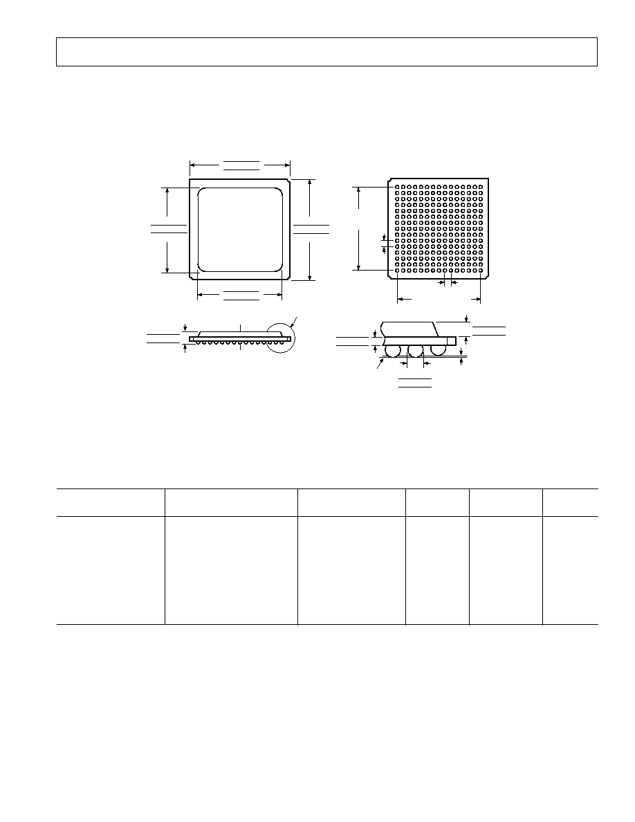
ADSP-21061/ADSP-21061L
≠47≠
REV. B
OUTLINE DIMENSIONS
Dimensions shown in inches and (mm).
Plastic Ball Grid Array (PBGA)
1
2
3
4
5
6
7
8
9
10
11
12
14
15
13
R
P
N
M
L
K
J
H
G
F
E
D
C
B
A
0.050
(1.27)
BSC
0.700
(17.78)
BSC
0.050 (1.27) BSC
0.700 (17.78) BSC
0.913 (23.20)
0.906 (23.00)
0.898 (22.80)
0.913 (23.20)
0.906 (23.00)
0.898 (22.80)
0.791 (20.10)
0.787 (20.00)
0.783 (19.90)
0.791 (20.10)
0.787 (20.00)
0.783 (19.90)
TOP VIEW
0.101 (2.57)
0.091 (2.32)
0.081 (2.06)
DETAIL A
SEATING
PLANE
0.051 (1.30)
0.047 (1.20)
0.043 (1.10)
0.006 (0.15) MAX
0.026 (0.65)
0.024 (0.61)
0.022 (0.57)
DETAIL A
0.035 (0.90)
0.030 (0.75)
0.024 (0.60)
BALL DIAMETER
NOTE
THE ACTUAL POSITION OF THE BALL GRID IS WITHIN
0.012 (0.30) OF ITS IDEAL POSITION RELATIVE TO THE PACKAGE
EDGES. THE ACTUAL POSITION OF EACH BALL IS WITHIN 0.004 (0.10)
OF ITS IDEAL POSITION RELATIVE TO THE BALL GRID.
ORDERING GUIDE
Case Temperature
On-Chip
Operating
Package
Part Number
Range
Instruction Rate
SRAM
Voltage
Option
ADSP-21061KS-133
0
∞C to +85∞C
33 MHz
1 Mbit
5 V
MQFP
ADSP-21061KS-160
0
∞C to +85∞C
40 MHz
1 Mbit
5 V
MQFP
ADSP-21061KS-200
0
∞C to +85∞C
50 MHz
1 Mbit
5 V
MQFP
ADSP-21061LKS-160
0
∞C to +85∞C
40 MHz
1 Mbit
3.3 V
MQFP
ADSP-21061LKS-176
0
∞C to +85∞C
44 MHz
1 Mbit
3.3 V
MQFP
ADSP-21061LAS-160
≠40
∞C Case to +85∞C Case
40 MHz
1 Mbit
3.3 V
MQFP
ADSP-21061LAS-176
≠40
∞C Case to +85∞C Case
44 MHz
1 Mbit
3.3 V
MQFP
ADSP-21061LKB-160
0
∞C to +85∞C
40 MHz
1 Mbit
3.3 V
PBGA
ADSP-21061LKB-176
0
∞C to +85∞C
44 MHz
1 Mbit
3.3 V
PBGA
The package options are as follows: the ADSP-21061 (5 V) is available in the 240-lead thermally enhanced package and the ADSP-21061L (3.3 V) is available in the
240-lead standard (no heat slug) package, and 225-Ball PBGA.
PRINTED IN U.S.A.
C3244b≠2.5≠6/00 (rev. B) 00170