ADSP-21161N DSP Microcomputer
a
Preliminary Technical Data
ADSP-21161N
DSP
Microcomputer
This information applies to a product under development. Its characteristics and
specifications are subject to change without notice. Analog Devices assumes no
obligation regarding future manufacturing unless otherwise agreed to in writing.
One Technology Way
http://www.analog.com/dsp
P.O. Box 9106
Tel: 1-800-ANALOG-D
Norwood MA 02062-9106
Fax: 1-781-461-3010
U.S.A.
Analog Devices Inc., 2000
REV. PrA
SUMMARY
·
High performance 32-bit DSP--applications in
audio, medical, military, wireless communica-
tions, graphics, imaging, motor-control, and te-
lephony
·
Super Harvard Architecture--four independent
buses for dual data fetch, instruction fetch, and
nonintrusive, zero-overhead I/O
·
Code-compatible to all other SHARC Family
DSPs
·
Single-Instruction-Multiple-Data (SIMD) com-
putational architecture--two 32-bit IEEE float-
ing-point computation units, each with a
multiplier, ALU, shifter, and register file
·
Serial ports offer I
2
S support via 8 programma-
ble and simultaneous receive and transmit pins,
which supports up to 16 transmit or 16 receive
channels of audio
·
Integrated peripherals--integrated I/O proces-
sor, 1 Mbit on-chip dual-ported SRAM,
SDRAM controller, glueless multiprocessing
features, and I/O ports (serial, link, external bus,
SPI, & JTAG)
·
ADSP-21161N supports 32-bit fixed, 32-bit
float, and 40-bit floating point formats.
KEY FEATURES
·
100 MHz (10 ns) core instruction rate
·
Single-cycle instruction execution, including
SIMD operations in both computational units
·
600 MFLOPS peak and 400 MFLOPs sustained
performance
·
225-ball 17x17mm PBGA package
·
1 Mbit on-chip dual-ported SRAM (0.5 Mbit
block 0, 0.5 Mbit block 1) for independent ac-
cess by core processor and DMA
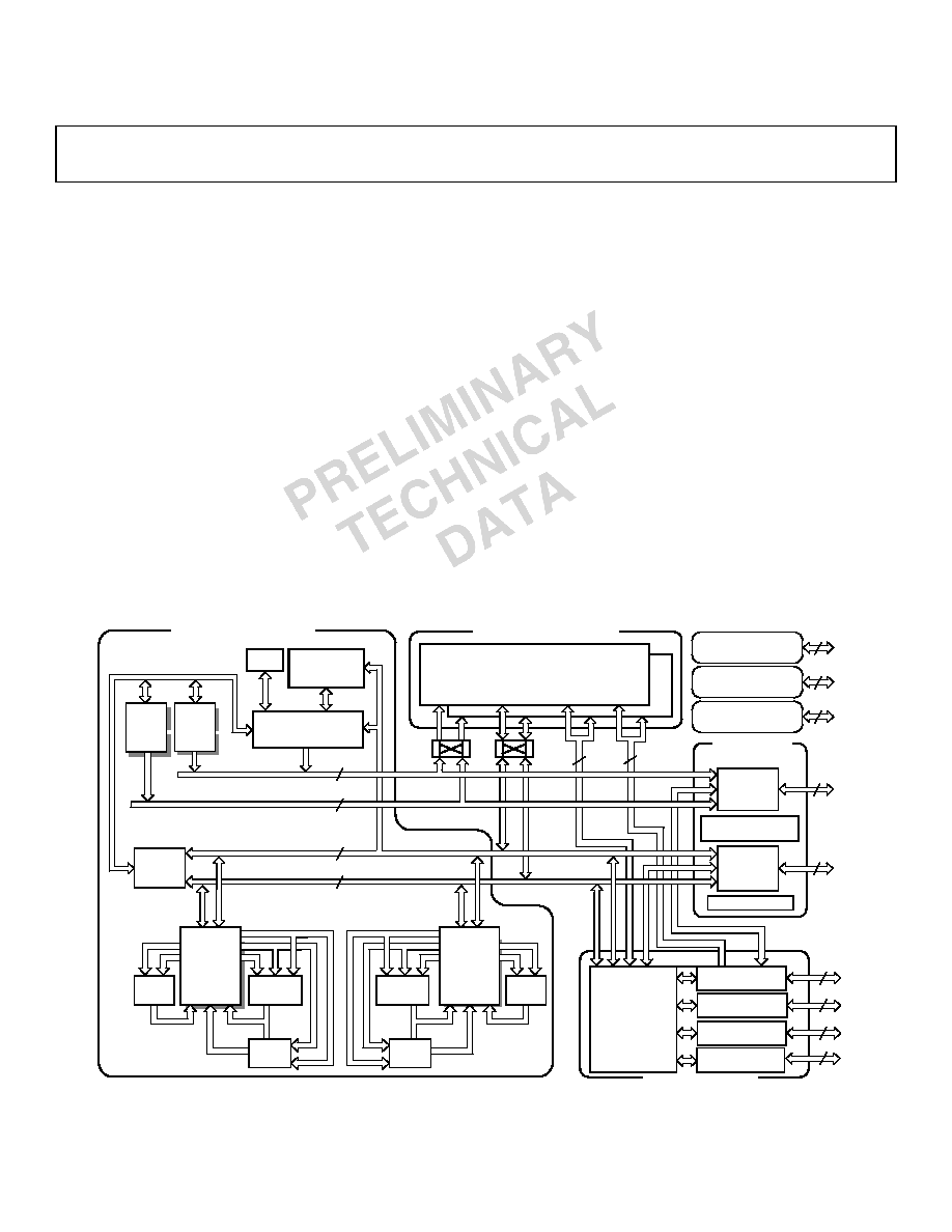
Figure 1 ADSP-21161N Functional Block Diagram
S P I P O R T S
( 1 )
S E R I A L P O R T S
( 4 )
L I N K P O R T S
( 2 )
D M A
C ON T R OL L E R
M U L T
A L U
B A R R E L
S H I F T E R
D A T A
R E G I S T E R
F I L E
(P E y )
16 x 4 0 - B I T
M U L T
A L U
B A R R E L
S H I F T E R
D A T A
R E G I S T E R
F I L E
( P E x )
16 x 4 0 - B I T
5
1 6
2 0
4
I O P
R E G I S T E R S
(
MEMORY MAPPED)
C O N T R O L ,
S T A T U S , &
D A T A B U F F E R S
I / O P R O C ES S O R
T I M E R
I N S T R U C T I ON
C A C H E
3 2 x 4 8 - BI T
A D D R
D A T A
D A TA
D A T A
A D D R
A D D R
D A T A
A D D R
T W O I N D E P E N D E N T
D U A L - P OR T E D B L O C K S
PR O C ES S O R PO R T
I / O PO R T
B
L
O
C
K
0
B
L
O
C
K
1
D U A L - P O R T E D S R A M
H OS T P OR T
A D D R B U S
M U X
I O A
1 8
I O D
6 4
MULTIPROCESSOR
INTERFACE
E X T E R N A L
P O R T
D A T A B U S
M U X
3 2
2 4
3 2
P M A D D R E S S B U S
D M A D D R E S S B U S
P M D A T A B U S
D M D A T A B U S
B U S
C O N N E C T
( P X )
D A G 1
8 x 4 x 3 2
3 2
6 4
6 4
C O R E P R O C E S SO R
P R O GR A M
S E Q U E N C E R
D A G 2
8 x 4 x 3 2
J T A G
T E S T & E M U L A T I ON
6
GP I O
F L A G S
S D R A M
C ON T R OL L E R
12
8

July 2000
ADSP-21161N Preliminary Data Sheet
For current information contact Analog Devices at (781) 461-3881
This information applies to a product under development. Its characteristics and specifications are subject to change with-
out notice. Analog Devices assumes no obligation regarding future manufacturing unless otherwise agreed to in writing.
2
REV. PrA
KEY FEATURES (continued)
·
400 million fixed-point MACs sustained performance
·
Dual Data Address Generators (DAGs) with modulo and bit-reverse addressing
·
Zero-overhead looping with single-cycle loop setup, providing efficient program sequencing
·
IEEE 1149.1 JTAG standard test access port and on-chip emulation
·
Single Instruction Multiple Data (SIMD) architecture provides:
·
Two computational processing elements
·
Concurrent execution--Each processing element executes the same instruction, but oper-
ates on different data
·
Code compatibility--At assembly level, uses the same instruction set as other SHARC
DSPs
·
Parallelism in busses and computational units allows:
·
Single-cycle execution (with or without SIMD) of: a multiply operation, an ALU opera-
tion, a dual memory read or write, and an instruction fetch
·
Transfers between memory and core at up to four 32-bit floating- or fixed-point words
per cycle, sustained 1.6 Gigabytes/second bandwidth
·
Accelerated FFT butterfly computation through a multiply with add and subtract
·
DMA Controller supports:
·
14 zero-overhead DMA channels for transfers between ADSP-21161N internal memory
and external memory, external peripherals, host processor, serial ports, link ports or Serial
Peripheral Interface (SPI) interface
·
64-bit background DMA transfers at core clock speed, in parallel with full-speed proces-
sor execution
·
800 Mbytes/s transfer rate over IOP bus
·
Host processor interface to 8-, 16- and 32-bit microprocessors, the host can directly
read/write ADSP-21161N IOP registers.
·
32-bit (or up to 48-bit) wide synchronous External Port provides:
·
Glueless connection to asynchronous, SBSRAM and SDRAM external memories
·
Memory interface supports programmable wait state generation and wait mode for
off-chip memory
·
Up to 50 MHz operation for non-SDRAM accesses
·
1:2, 1:3, 1:4, 1:6, 1:8 clock in to Core Clock frequency multiply ratios
·
24-bit address, 32-bit data bus. 16 additional data lines via multiplexed link port data
pins allow complete 48-bit wide data bus for single-cycle external instruction execution
·
Direct reads and writes of IOP registers from host or other 21161N DSPs
·
64 Mega-word address range for off-chip SRAM and SBSRAM memories
·
32-48, 16-48, 8-48 execution packing for executing instruction directly from 32-bit,
16-bit, or 8-bit wide external memories
·
32-48, 16-48, 8-48, 32-32/64, 16-32/64, 8-32/64, data packing for DMA transfers di-
rectly from 32-bit, 16-bit, or 8-bit wide external memories to and from internal 32-, 48-,
or 64-bit internal memory
·
Can be configured to have 48-bit wide external data bus possible, if link ports are not

This information applies to a product under development. Its characteristics and specifications are subject to change with-
out notice. Analog Devices assumes no obligation regarding future manufacturing unless otherwise agreed to in writing.
ADSP-21161N Preliminary Data Sheet
July 2000
For current information contact Analog Devices at (781) 461-3881
3
REV. PrA
used. The link port data lines are multiplexed with the data lines D0 to D15 and is en-
abled through control bits in SYSCON
·
SDRAM Controller for glueless interface to low cost external memory
·
Zero wait state, 100 MHz operation for most accesses
·
Extended external memory banks (64 M-words) for SDRAM accesses
·
Page sizes up to 2048 words
·
An SDRAM controller supports SDRAM in any and all memory banks
·
Support for interface to run at core clock & half the core clock frequency
·
Support for 16 Mbits, 64 Mbits, 128 Mbits, and 256 Mbits with SDRAM data bus con-
figurations of x4, x8 and x16
·
254 Mega-word address range for off-chip SDRAM memory
·
Multiprocessing support provides:
·
Glueless connection for scalable DSP multiprocessing architecture
·
Distributed on-chip bus arbitration for parallel bus connect of up to six ADSP-21161Ns,
global memory and a host
·
Two 8-bit wide link ports for point-to-point connectivity and array multiprocessing be-
tween ADSP-21161Ns
·
400 Mbytes/s transfer rate over parallel bus
·
200 Mbytes/s transfer rate over link ports
·
Serial Ports provide:
·
Four 50 Mbit/s synchronous serial ports with companding hardware
·
8 bi-directional serial data pins, configurable as either a transmitter or receiver
·
I
2
S Support, programmable direction for 8 simultaneous Receive and Transmit channels,
or up to either 16 Transmit channels or 16 Receive channels.
·
TDM support for T1 and E1 interfaces, and 128 TDM channel support for newer tele-
phony interfaces such as H.100/H.110
·
Companding selection on a per channel basis in TDM mode
·
Serial Peripheral Interface (SPI)
·
Slave Serial boot through SPI from a Master SPI device
·
Full-duplex operation
·
Master-Slave mode multi-master support
·
Open drain outputs
·
Programmable baud rates, clock polarities and phases
·
12 Programmable I/O pins
July 2000
ADSP-21161N Preliminary Data Sheet
For current information contact Analog Devices at (781) 461-3881
This information applies to a product under development. Its characteristics and specifications are subject to change with-
out notice. Analog Devices assumes no obligation regarding future manufacturing unless otherwise agreed to in writing.
4
REV. PrA
GENERAL DESCRIPTION
The ADSP-21161N SHARC DSP is the first low-cost derivative of the ADSP-21160 featuring Analog
Devices' Super Harvard Architecture. Easing portability, the ADSP-21161N is source code compatible
with the ADSP-21160 and with first generation ADSP-2106x SHARCs in SISD (Single Instruction,
Single Data) mode. Like other SHARCs, the ADSP-21161N is a 32-bit processor that is optimized for
high performance DSP applications. The ADSP-21161N includes a 100 MHz core, a dual-ported
on-chip SRAM, an integrated I/O processor with multiprocessing support, and multiple internal busses
to eliminate I/O bottlenecks.
The ADSP-21161N offers a Single-Instruction-Multiple-Data (SIMD) architecture, which was first
offered in the ADSP-21160. Using two computational units (ADSP-2106x SHARCs have one), the
ADSP-21161N can double cycle performance versus the ADSP-2106x on a range of DSP algorithms.
Fabricated in a state of the art, high speed, low power CMOS process, the ADSP-21161N has a 10 ns
instruction cycle time. With its SIMD computational hardware running at 100 MHz, the
ADSP-21161N can perform 600 million math operations per second.
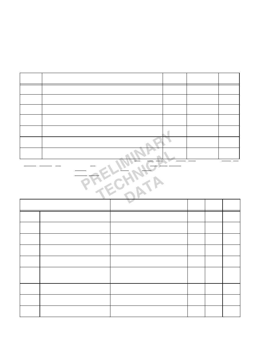
Table 1
shows performance
benchmarks for the ADSP-21161N.
The ADSP-21161N continues SHARC's industry leading standards of integration for DSPs,
combining a high performance 32-bit DSP core with integrated, on-chip system features. These
features include a 1 Mbit dual ported SRAM memory, host processor interface, I/O processor that
supports 14 DMA channels, four serial ports, two link ports, SDRAM controller, SPI interface, external
parallel bus, and glueless multiprocessing.
Figure 1 on page 1
shows a block diagram of the ADSP-21161N, illustrating the following architectural
features:
·
Two processing elements, each made up of an ALU, Multiplier, Shifter and Data Register File
·
Data Address Generators (DAG1, DAG2)
·
Program sequencer with instruction cache
·
PM and DM buses capable of supporting four 32-bit data transfers between memory and the core
every core processor cycle
·
Interval timer
Table 1 ADSP-21161N Benchmarks (at 100 MHz)
Benchmark Algorithm
Speed (at 100 MHz)
1024 Point Complex FFT (Radix 4, with reversal)
92 s
FIR Filter (per tap)
5 ns
IIR Filter (per biquad)
20 ns
Matrix Multiply (pipelined)
[3x3] * [3x1]
[4x4] * [4x1]
45 ns
80 ns
Divide (y/x)
30 ns
Inverse Square Root
45 ns
This information applies to a product under development. Its characteristics and specifications are subject to change with-
out notice. Analog Devices assumes no obligation regarding future manufacturing unless otherwise agreed to in writing.
ADSP-21161N Preliminary Data Sheet
July 2000
For current information contact Analog Devices at (781) 461-3881
5
REV. PrA
·
On-Chip SRAM (1 Mbit)
·
SDRAM Controller for glueless interface to SDRAMs
·
External port that supports:
·
Interfacing to off-chip memory peripherals
·
Glueless multiprocessing support for six ADSP-21161N SHARCs
·
Host port read/write of IOP registers
·
DMA controller
·
Four serial ports
·
Two link ports
·
SPI-compatible interface
·
JTAG test access port
·
12 General Purpose I/O Pins
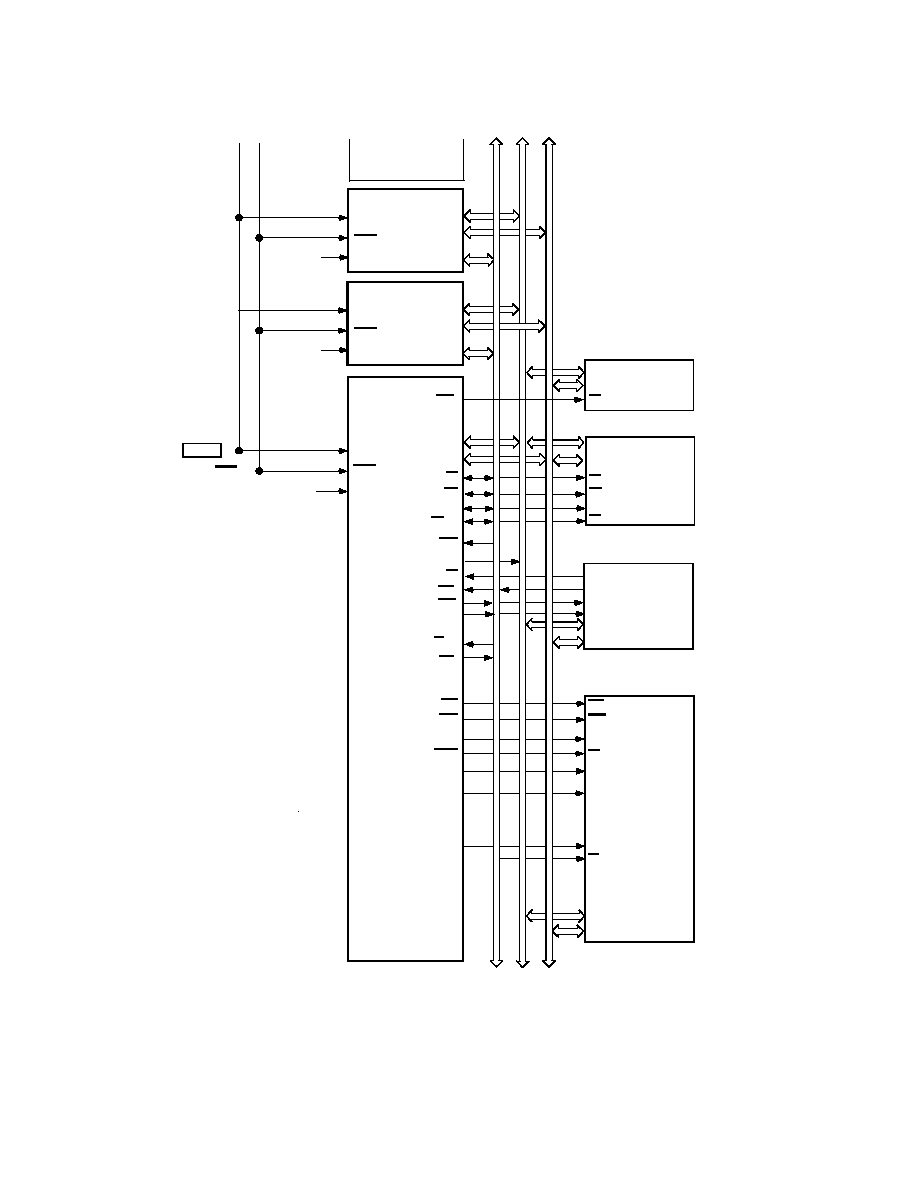
Figure 2
shows a typical single-processor system. A multi-processing system appears in
Figure 5 on
page 11
.
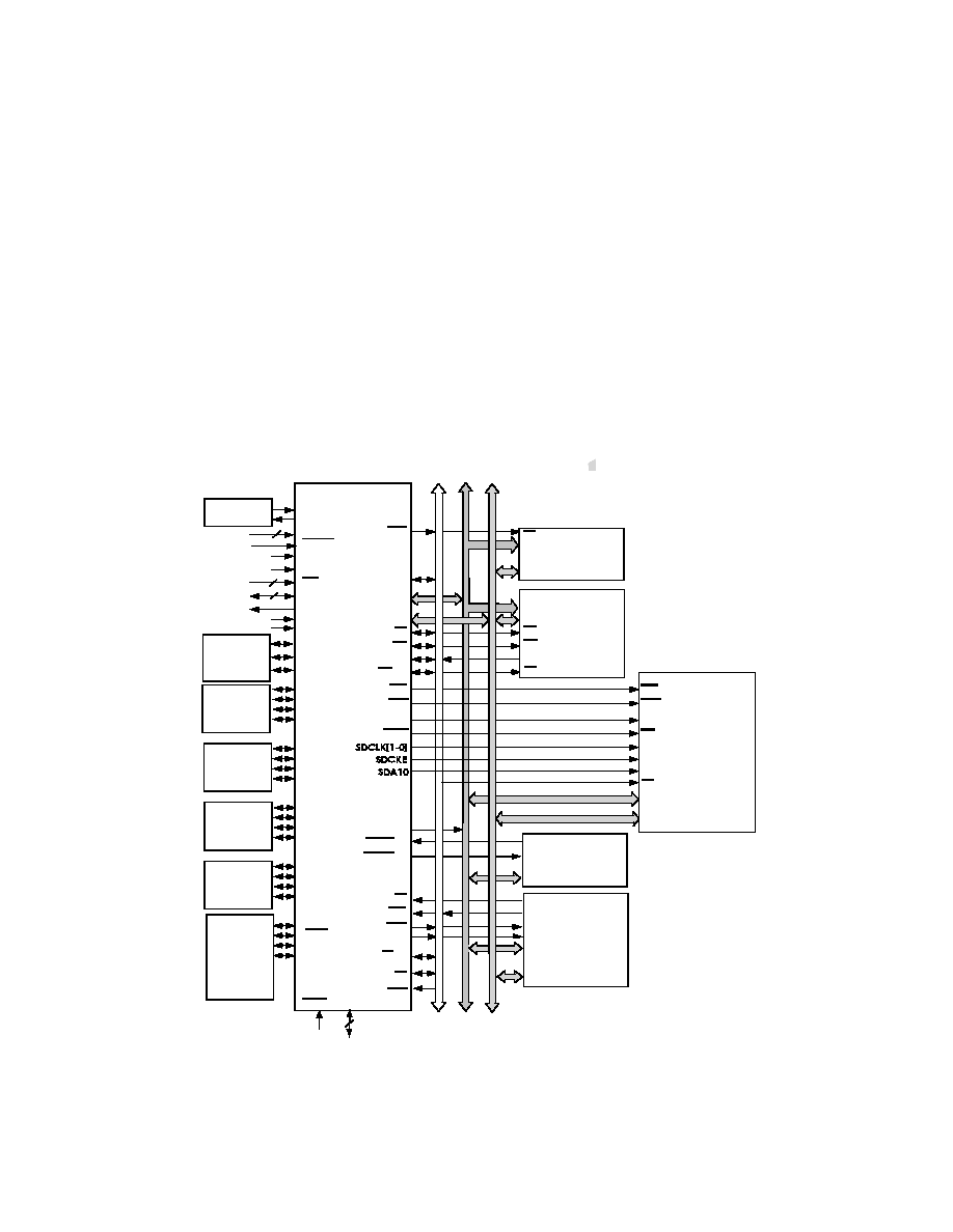
Figure 2 ADSP-21161N System
DMA DEVICE
(OPTIONAL)
D A TA
C LK O U T
DMAR1-2
DMAG1-2
R E D Y
A D D R
D A TA
H O S T
P R O C E S S O R
IN TE R F A C E
( O P T IO N A L )
3
1 2
C LO C K
C LK IN
X TA L
IRQ2-0
2
C LK _ C F G 1 -0
E B O O T
LB O O T
F LA G 1 1 -0
TIM E X P
CLKDBL
RESET
J TA G
7
SBTS
A D S P - 2 1 1 6 1 N
BMS
LIN K
D E V IC E S
(2 M A X )
( O P T IO N A L )
Lx C LK
Lx A C K
L x D A T7 -0
SC LK 0
D 0 B
D 0 A
F S0
S E R IA L
D E V IC E
( O P T IO N A L )
CS
B O O T
E P R O M
( O P T IO N A L )
A D D R
M E M O R Y
A N D
P E R IP H E R A LS
( O P T IO N A L )
OE
D A TA
CS
RD
RAS
A C K
BR1-6
R P BA
ID 2 -0
PA
HBG
HBR
SDWE
MS3-0
WR
D A TA 4 7 -1 6
D A TA
A D D R
CS
A C K
WE
A D D R 2 3 -0
DA
T
A
C
ON
T
R
OL
A
DD
R
E
S
S
B R S T
S D R A M
( O P T IO N A L )
S C LK 1
D 1 B
D 1 A
F S 1
S E R IA L
D E V IC E
( O P T IO N A L )
S C LK 2
D 2 B
D 2 A
F S 2
S E R IA L
D E V IC E
( O P T IO N A L )
S C LK 3
D 3 B
D 3 A
F S 3
S E R IA L
D E V IC E
( O P T IO N A L )
S P IC LK
M IS O
M O S I
SPDS
SPI-
C O M P A TIB LE
D E V IC E
(H O S T O R
S L A V E )
( O P T IO N A L )
D A TA
CAS
RAS
D Q M
WE
A D D R
CS
A 1 0
C K E
C LK
D Q M
CAS

July 2000
ADSP-21161N Preliminary Data Sheet
For current information contact Analog Devices at (781) 461-3881
This information applies to a product under development. Its characteristics and specifications are subject to change with-
out notice. Analog Devices assumes no obligation regarding future manufacturing unless otherwise agreed to in writing.
6
REV. PrA
ADSP-21161N Family Core Architecture
The ADSP-21161N includes the following architectural features of the ADSP-21100 family core. The
ADSP-21161N is code compatible at the assembly level with the ADSP-21160, ADSP-21060,
ADSP-21061, and ADSP-21062 and ADSP-21065L.
SIMD Computational Engine
The ADSP-21161N contains two computational processing elements that operate as a Single
Instruction Multiple Data (SIMD) engine. The processing elements are referred to as PEX and PEY
and each contains an ALU, multiplier, shifter and register file. PEX is always active, and PEY may be
enabled by setting the PEYEN mode bit in the MODE1 register. When this mode is enabled, the same
instruction is executed in both processing elements, but each processing element operates on different
data. This architecture is efficient at executing math intensive DSP algorithms.
Entering SIMD mode also has an effect on the way data is transferred between memory and the
processing elements. When in SIMD mode, twice the data bandwidth is required to sustain
computational operation in the processing elements. Because of this requirement, entering SIMD mode
also doubles the bandwidth between memory and the processing elements. When using the DAGs to
transfer data in SIMD mode, two data values are transferred with each access of memory or the register
file.
Independent, Parallel Computation Units
Within each processing element is a set of computational units. The computational units consist of an
arithmetic/logic unit (ALU), multiplier and shifter. These units perform single-cycle instructions. The
three units within in each processing element are arranged in parallel, maximizing computational
throughput. Single multi-function instructions execute parallel ALU and multiplier operations. In
SIMD mode, the parallel ALU and multiplier operations occur in both processing elements. These
computation units support IEEE 32-bit single-precision floating-point, 40-bit extended precision
floating-point, and 32-bit fixed-point data formats.
Data Register File
A general purpose data register file is contained in each processing element. The register files transfer
data between the computation units and the data buses, and store intermediate results. These 10-port,
32-register (16 primary, 16 secondary) register files, combined with the ADSP-21100 enhanced
Harvard architecture, allow unconstrained data flow between computation units and internal memory.
The registers in PEX are referred to as R0-R15 and in PEY as S0-S15.
Single-Cycle Fetch of Instruction and Four Operands
The ADSP-21161N features an enhanced Harvard architecture in which the data memory (DM) bus
transfers data and the program memory (PM) bus transfers both instructions and data (see
Figure 1 on
page 1
). With the ADSP-21161N's separate program and data memory buses and on-chip instruction
cache, the processor can simultaneously fetch four operands (two over each data bus) and an instruction
(from the cache), all in a single cycle.
Instruction Cache
The ADSP-21161N includes an on-chip instruction cache that enables three-bus operation for fetching
an instruction and four data values. The cache is selective--only the instructions whose fetches conflict
with PM bus data accesses are cached. This cache allows full-speed execution of core, looped operations
such as digital filter multiply-accumulates and FFT butterfly processing.

This information applies to a product under development. Its characteristics and specifications are subject to change with-
out notice. Analog Devices assumes no obligation regarding future manufacturing unless otherwise agreed to in writing.
ADSP-21161N Preliminary Data Sheet
July 2000
For current information contact Analog Devices at (781) 461-3881
7
REV. PrA
Data Address Generators With Hardware Circular Buffers
The ADSP-21161N's two data address generators (DAGs) are used for indirect addressing and let you
implement circular data buffers in hardware. Circular buffers allow efficient programming of delay lines
and other data structures required in digital signal processing, and are commonly used in digital filters
and Fourier transforms. The two DAGs of the ADSP-21161N contain sufficient registers to allow the
creation of up to 32 circular buffers (16 primary register sets, 16 secondary). The DAGs automatically
handle address pointer wrap-around, reducing overhead, increasing performance, and simplifying
implementation. Circular buffers can start and end at any memory location.
Flexible Instruction Set
The 48-bit instruction word accommodates a variety of parallel operations, for concise programming.
For example, the ADSP-21161N can conditionally execute a multiply, an add, and a subtract in both
processing elements, while branching, all in a single instruction.
ADSP-21161N Memory and I/O Interface Features
Augmenting the ADSP-21100 family core, the ADSP-21161N adds the following architectural
features:
Dual-Ported On-Chip Memory
The ADSP-21161N contains one megabit of on-chip SRAM, organized as two blocks of 0.5 Mbits
each, which can be configured for different combinations of code and data storage. Each memory block
is dual-ported for single-cycle, independent accesses by the core processor and I/O processor. The
dual-ported memory in combination with three separate on-chip buses allow two data transfers from
the core and one from the I/O processor, in a single cycle. On the ADSP-21161N, the memory can be
configured as a maximum of 32K words of 32-bit data, 64K words of 16-bit data, 21.25K words of
48-bit instructions (or 40-bit data), or combinations of different word sizes up to one megabit. All of
the memory can be accessed as 16-bit, 32-bit, 48-bit, or 64-bit words. A 16-bit floating-point storage
format is supported that effectively doubles the amount of data that may be stored on-chip. Conversion
between the 32-bit floating-point and 16-bit floating-point formats is done in a single instruction.
While each memory block can store combinations of code and data, accesses are most efficient when
one block stores data, using the DM bus for transfers, and the other block stores instructions and data,
using the PM bus for transfers. Using the DM bus and PM bus in this way, with one dedicated to each
memory block, assures single-cycle execution with two data transfers. In this case, the instruction must
be available in the cache.
July 2000
ADSP-21161N Preliminary Data Sheet
For current information contact Analog Devices at (781) 461-3881
This information applies to a product under development. Its characteristics and specifications are subject to change with-
out notice. Analog Devices assumes no obligation regarding future manufacturing unless otherwise agreed to in writing.
8
REV. PrA
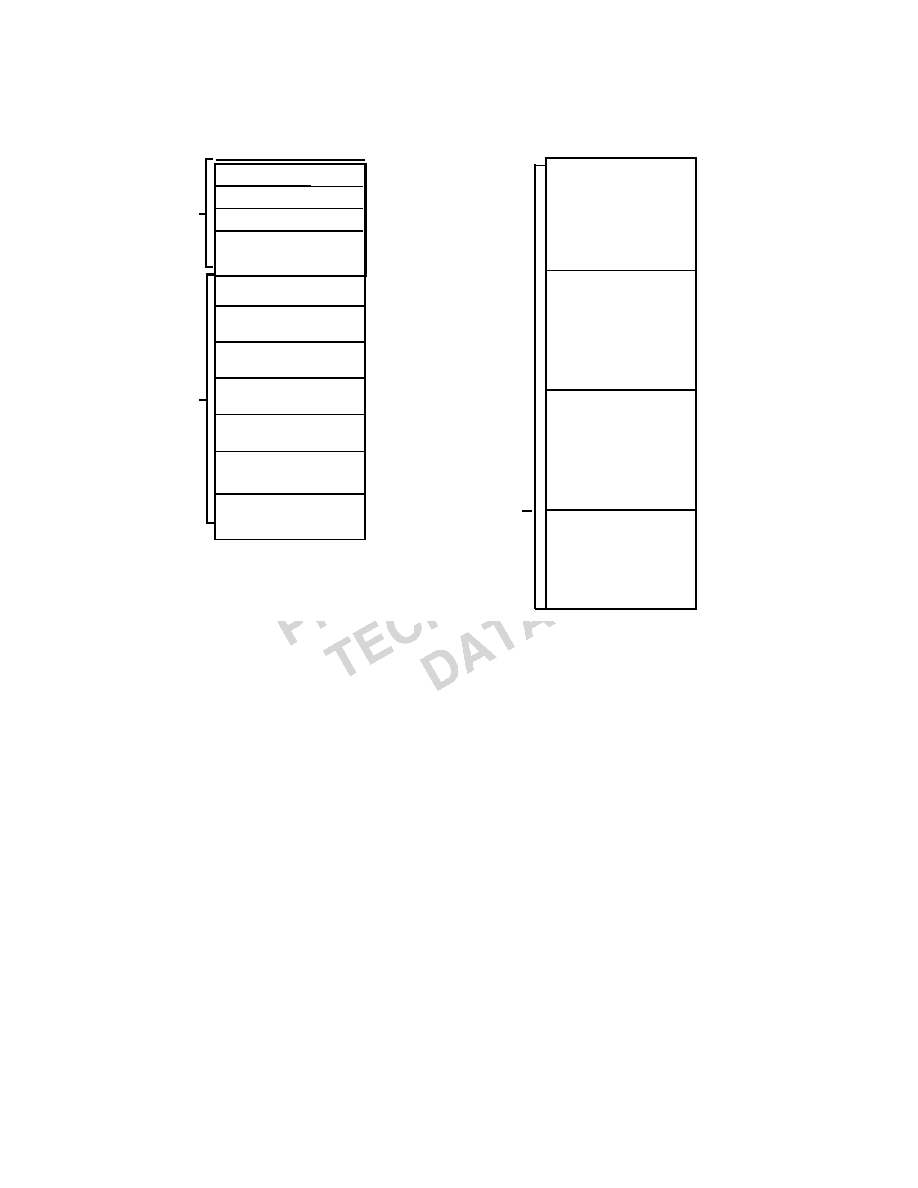
Figure 3 ADSP-21161N Memory Map
Off-Chip Memory and Peripherals Interface
The ADSP-21161N's external port provides the processor's interface to off-chip memory and
peripherals. The 64-megaword off-chip address space (254-megaword if all SDRAM) is included in the
ADSP-21161N's unified address space. The separate on-chip buses--for PM addresses, PM data, DM
addresses, DM data, I/O addresses, and I/O data--are multiplexed at the external port to create an
external system bus with a single 24-bit address bus and a single 32-bit data bus. Every access to external
memory is based on an address that fetches a 32-bit word. When fetching an instruction from external
memory, two 32-bit data locations are being accessed for packed instructions. Unused link port lines
can also be used as additional data lines DATA[0]-DATA[15], allowing single cycle execution of
instructions from external memory at up to 100 MHz.
Figure 4 on page 10
shows the alignment of
various accesses to external memory.
The external port supports asynchronous, synchronous, and synchronous burst accesses. Synchronous
burst SRAM can be interfaced gluelessly. The ADSP-21161N also can interface gluelessly to SDRAM.
Addressing of external memory devices is facilitated by on-chip decoding of high-order address lines to
generate memory bank select signals. Separate control lines are also generated for simplified addressing
of page-mode DRAM. The ADSP-21161N provides programmable memory wait states and external
memory acknowledge controls to allow interfacing to memory and peripherals with variable access,
hold, and disable time requirements.
0x000A 0000 - 0x000A 7F FF (Blk 1)
0x0002 8000 - 0x0002 9FFF (Blk 1)
0x0005 0000 - 0x0005 3FFF (Blk 1)
0x0010 0000 - 0x0011 FF FF
0x0004 0000 - 0x0004 3FFF (Blk 0)
0x0008 0000 - 0x0008 7FFF (Blk 0)
0x0012 0000 - 0x0013 FF FF
0x0014 0000 - 0x0015 FF FF
0x0016 0000 - 0x0017 FF FF
0x001A 0000 - 0x001B FFFF
0x001F FFFF
0x001C FFFF
0x0000 0000 - 0x0001 FFFF
0x0002 0000 - 0x0002 1FFF (Blk 0)
0x0020 0000
Bank 1
!
!
!
! MS0*
Bank 2
!
!
!
! MS1*
Bank 3
!
!
!
! MS2*
!
!
!
! MS
3
*
M em ory
Internal
M em ory
Space
IO P REG IST ERS
IO P R egisters o f
ADS P-21161N with ID=001
Long Wo rd Add ressin g
Sho rt Word Add ressin g
IO P R egisters o f
ADS P-21161N with ID=010
IO P R egisters o f
ADS P-21161N with ID=100
IO P R egisters o f
ADS P-21161N with ID=011
IO P R egisters o f
ADS P-21161N with ID=101
IO P R egisters o f
ADS P-21161N with ID=110
Normal Word Ad dressin g
ADDRE SS
Reserved
M ulti-
processor
Space
Bank 0
0x03FF FFFF (S DRAM )
0x00FF FFFF (Non-S DRAM )
0x0400 0000
0x07FF FFFF (S DRAM )
0x04FF FFFF (Non-S DRAM )
0x0800 0000
0x0BFF FFFF (S DRAM )
0x08FF FFFF (Non-S DRAM )
0x0C00 0000
0x0FFF FFFF (SDRAM )
0x0CFF FFFF (Non-S DRAM )
External
M em ory
Space
*Bank S izes Are Fixed

This information applies to a product under development. Its characteristics and specifications are subject to change with-
out notice. Analog Devices assumes no obligation regarding future manufacturing unless otherwise agreed to in writing.
ADSP-21161N Preliminary Data Sheet
July 2000
For current information contact Analog Devices at (781) 461-3881
9
REV. PrA
SDRAM Interface
The SDRAM interface enables the ADSP-21161N to transfer data to and from synchronous DRAM
(SDRAM) at the core clock frequency or one-half the core clock frequency. The synchronous approach,
coupled with the core clock frequency, supports data transfer at a high throughput--up to 400
Mbytes/sec. for x32 transfers and 600 Mbytes/sec. for x48 transfers.
The SDRAM interface provides a glueless interface with standard SDRAMs--16 Mb, 64 Mb, 128 Mb,
and 256 Mb--and includes options to support additional buffers between the ADSP-21161N and
SDRAM. The SDRAM interface is extremely flexible and provides capability for connecting SDRAMs
to any one of the ADSP-21161N's four external memory banks, with up to all four banks mapped to
SDRAM.
Systems with several SDRAM devices connected in parallel may require buffering to meet overall
system timing requirements. The ADSP-21161N supports pipelining of the address and control signals
to enable such buffering between itself and multiple SDRAM devices.
DMA Controller
The ADSP-21161N's on-chip DMA controller allows zero-overhead data transfers without processor
intervention. The DMA controller operates independently and invisibly to the processor core, allowing
DMA operations to occur while the core is simultaneously executing its program instructions. DMA
transfers can occur between the ADSP-21161N's internal memory and external memory, external
peripherals, or a host processor. DMA transfers can also occur between the ADSP-21161N's internal
memory and its serial ports, link ports, or the Serial Peripheral Interface (SPI)-compatible port.
External bus packing and unpacking of 16-, 32-, 48-, or 64-bit words in internal memory is
performed during DMA transfers from either 8-, 16-, or 32-bit wide external memory. Fourteen
channels of DMA are available on the ADSP-21161N--two are shared between the SPI interface and
the link ports, eight via the serial ports, and four via the processor's external port (for either host
processor, other ADSP-21161Ns, memory or I/O transfers). Programs can be downloaded to the
ADSP-21161N using DMA transfers. Asynchronous off-chip peripherals can control two DMA
channels using DMA Request/Grant lines (DMAR
1-2
, DMAG
1-2
). Other DMA features include
interrupt generation upon completion of DMA transfers, two-dimensional DMA, and DMA chaining
for automatic linked DMA transfers.
July 2000
ADSP-21161N Preliminary Data Sheet
For current information contact Analog Devices at (781) 461-3881
This information applies to a product under development. Its characteristics and specifications are subject to change with-
out notice. Analog Devices assumes no obligation regarding future manufacturing unless otherwise agreed to in writing.
10
REV. PrA
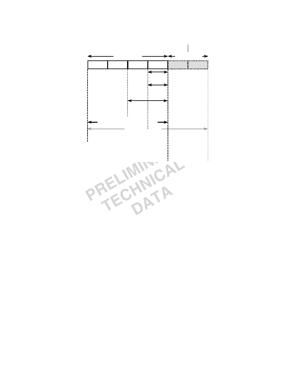
Figure 4 ADSP-21161N External Data Alignment Options
Multiprocessing
The ADSP-21161N offers powerful features tailored to multi-processing DSP systems. The external
port and link ports provide integrated glueless multiprocessing support.
The external port supports a unified address space (see
Figure 3 on page 8
) that allows direct
interprocessor accesses of each ADSP-21161N's internal memory-mapped (I/O processor) registers. All
other internal memory can be indirectly accessed via DMA transfers initiated via the programming of
the IOP DMA parameter and control registers. Distributed bus arbitration logic is included on-chip
for simple, glueless connection of systems containing up to six ADSP-21161Ns and a host processor.
Master processor change over incurs only one cycle of overhead. Bus arbitration is selectable as either
fixed or rotating priority. Bus lock allows indivisible read-modify-write sequences for semaphores. A
vector interrupt is provided for interprocessor commands. Maximum throughput for interprocessor
data transfer is 400 Mbytes/s over the external port.
Two link ports provide for a second method of multiprocessing communications. Each link port can
support communications to another ADSP-21161N. A large multiprocessor system can be constructed
in a 2D fashion, using the link ports. The ADSP-21161N running at 100 MHz has a maximum
throughput for interprocessor communications over the links of 200 Mbytes per second. You can use
the link ports and cluster multiprocessing concurrently or independently.
47
48-bit Instruction Fetch
(No Packing)
Extra Data Lines
DATA[15-0] Are Only
Accessible If Link Ports
Are Disabled. Enable
These Additional Data
Lines By setting
IPACK[1:0] = 01 In
SYSCON.
0
7
8
15
16
23
24
31
32
39
40
Float or Fixed, D31-D0, 32-bit Packed
16-bit Packed DMA Data
16-bit Packed Instruction Execution
PROM
BOOT
DATA 47-16
L1DATA[7:0] L0DATA[7:0]
DATA 15-8 DATA 7-0
8-bit Packed DMA Data
8-bit Packed Instruction Execution
32-bit Packed Instruction
DATA 15-0
This information applies to a product under development. Its characteristics and specifications are subject to change with-
out notice. Analog Devices assumes no obligation regarding future manufacturing unless otherwise agreed to in writing.
ADSP-21161N Preliminary Data Sheet
July 2000
For current information contact Analog Devices at (781) 461-3881
11
REV. PrA
Figure 5 ADSP-21161N Shared Memory Multiprocessing System
A C K
OE
A DDR
DATA
CS
WE
G LO BAL
M EM ORY
A ND
PERIPH ERA LS
(O P TIO N A L)
CO
N
T
R
O
L
A DSP-2116X #1
A DDR23-0
DATA47-16
C O NTRO L
A DSP-21161 #3
ID2-0
RESET
C LK IN
3
A DSP-21161 #4
C LO C K
A DDR
DATA
SDRA M
(O P TIO N A L)
CS
A DDR
DATA
BO O T
EPROM
(O P TIO N A L)
ID2-0
RESET
C LK IN
CO
N
T
R
O
L
AD
D
R
E
S
S
DA
T
A
CO
N
T
R
O
L
AD
D
R
E
S
S
DA
T
A
A DDR23-0
DATA47-16
C O NTRO L
A DSP-21161 #2
ID2-0
RESET
C LK IN
2
1
A DDR
DATA
H O ST
PRO CESSO R
IN TERFA CE
(O P TIO N A L)
WE
RAS
CAS
DQ M
CLK
A10
CKE
CS
DATA47-16
SDWE
RAS
CAS
DQ M
SDCLK[1-0]
SDA10
SDCKE
BR6-2
RD
MS3-0
SBTS
C LK O UT
CS
A C K
BR1
REDY
HBG
HBR
WR
BMS
A DDR23-0
RESET

July 2000
ADSP-21161N Preliminary Data Sheet
For current information contact Analog Devices at (781) 461-3881
This information applies to a product under development. Its characteristics and specifications are subject to change with-
out notice. Analog Devices assumes no obligation regarding future manufacturing unless otherwise agreed to in writing.
12
REV. PrA
Link Ports
The ADSP-21161N features two 8-bit link ports that provide additional I/O capabilities. With the
capability of running at 100 MHz rates, each link port can support 100 Mbytes/s. Link port I/O is
especially useful for point-to-point interprocessor communication in multiprocessing systems. The link
ports can operate independently and simultaneously, with a maximum data throughput of 200
Mbytes/s. Link port data is packed into 48- or 32-bit words and can be directly read by the core
processor or DMA-transferred to on-chip memory. Each link port has its own double-buffered input
and output registers. Clock/acknowledge handshaking controls link port transfers. Transfers are
programmable as either transmit or receive.
Serial Ports
The ADSP-21161N features four synchronous serial ports that provide an inexpensive interface to a
wide variety of digital and mixed-signal peripheral devices. Each serial port is made up of two data lines,
a clock and frame sync. The data lines can be programmed to be either transmit or receive.
The serial ports can operate up to half the clock rate of the core, providing each with a maximum data
rate of 50 Mbit/s. The serial data pins can be programmable as either a transmitter or receiver,
providing greater flexibility for serial communications. Serial port data can be automatically transferred
to and from on-chip memory via a dedicated DMA. Each of the serial ports offers a Time Division
Multiplex (TDM) multichannel mode, where two serial ports are TDM transmitters and two serial
ports are TDM receivers (SPORT0 RX paired with SPORT2 TX, SPORT1 RX paired with SPORT3
TX). Each of the serial ports also support the I
2
S protocol (an industry standard interface commonly
used by audio codecs, ADCs and DACs), with two data pins, allowing four I
2
S channels (using 2 I
2
S
stereo devices) per serial port, with a maximum of up to 16 I
2
S channels. The serial ports can operate
with little-endian or big-endian transmission formats, with word lengths selectable from 3 bits to 32
bits. For I
2
S mode, data-word lengths are selectable between 8 bits and 32 bits. They offer selectable
synchronization and transmit modes as well as optional
µ
-law or A-law companding. Serial port clocks
and frame syncs can be internally or externally generated.
Serial Peripheral (Compatible) Interface
Serial Peripheral Interface (SPI) is an industry standard synchronous serial link, enabling the
ADSP-21161N SPI-compatible port to communicate with other SPI-compatible devices. SPI is a
4-wire interface consisting of two data pins, one device select pin, and one clock pin. It is a full-duplex
synchronous serial interface, supporting both master and slave modes. It can operate in a multi-master
environment by interfacing with up to 4 other SPI-compatible devices, either acting as a master or slave
device. The ADSP-21161N SPI-compatible peripheral implementation also supports programmable
baud rate and clock phase/polarities. The ADSP-21161N SPI-compatible port supports the use of open
drain drivers to support the multi-master scenario and to avoid data contention.
Host Processor Interface
The ADSP-21161N host interface allows easy connection to standard microprocessor buses, either
8-bit, 16-bit, or 32-bit, with little additional hardware required. The host interface is accessed through
the ADSP-21161N's external port and is memory-mapped into the unified address space. Four
channels of DMA are available for the host interface; code and data transfers are accomplished with low
software overhead. The host processor requests the ADSP-21161N's external bus with the host bus
request (HBR), host bus grant (HBG), and ready (REDY) signals. The host can directly read and write
the internal IOP registers of the ADSP-21161N, and can access the DMA channel setup and mailbox
registers. DMA setup via a host would allow it to access any internal memory address via DMA
transfers. Vector interrupt support provides efficient execution of host commands.
This information applies to a product under development. Its characteristics and specifications are subject to change with-
out notice. Analog Devices assumes no obligation regarding future manufacturing unless otherwise agreed to in writing.
ADSP-21161N Preliminary Data Sheet
July 2000
For current information contact Analog Devices at (781) 461-3881
13
REV. PrA
General Purpose I/O Ports
The ADSP-21161N also contains twelve programmable, general purpose I/O pins that can function as
either input or output. As output, these pins can signal peripheral devices; as input, these pins can
provide the test for conditional branching.
Program Booting
The internal memory of the ADSP-21161N can be booted at system power-up from either an 8-bit
EPROM, a host processor, the SPI interface, or through one of the link ports. Selection of the boot
source is controlled by the Boot Memory Select (BMS), EBOOT (EPROM Boot), and Link/Host Boot
(LBOOT) pins. 8-, 16-, or 32-bit host processors can also be used for booting.
Phased Locked Loop and CLKIN Double Enable
The ADSP-21161N uses an on-chip Phase Locked Loop (PLL) to generate the internal clock for the
core. The CLK_CFG[1:0] pins are used to select ratios of 2:1, 3:1, and 4:1. In addition to the PLL
ratios, an additional CLKDBL pin can be used for additional clock ratio options. The (1x/2x CLKIN)
rate set by the CLKDBL pin determines the rate of the PLL input clock and the rate at which the
synchronous external port operates. With the combination of CLK_CFG[1:0] and CLKDBL, ratios of
2:1, 3:1, 4:1, 6:1, and 8:1 between the core and CLKIN are supported. See also
Figure 8 on page 28
.
Power Supplies
The ADSP-21161N has separate power supply connections for the internal (VDDINT), external
(VDDEXT), and analog (AVDD/AGND) power supplies. The internal and analog supplies must meet
the 1.8V requirement. The external supply must meet the 3.3V requirement. All external supply pins
must be connected to the same supply
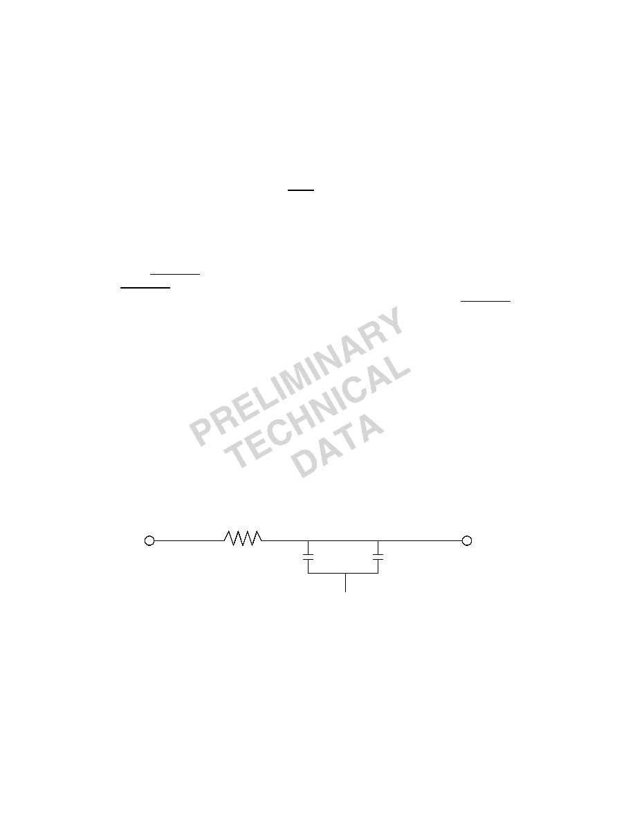
Note that the analog supply (AV
DD
) powers the ADSP-21161N's clock generator PLL. To produce a
stable clock, you must provide an external circuit to filter the power input to the AV
DD
pin. Place the
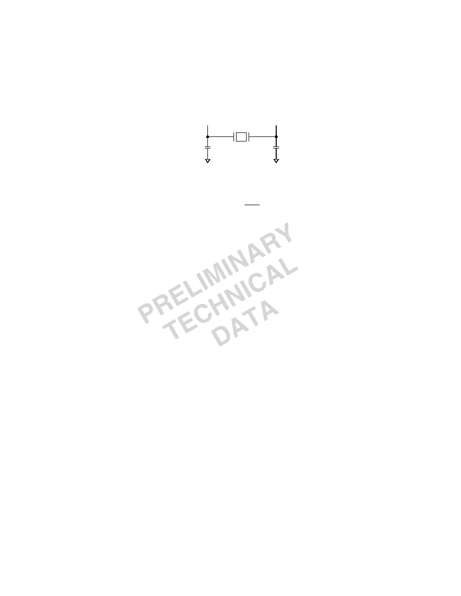
filter as close as possible to the pin. For an example circuit, see Figure 6. To prevent noise coupling, use
a wide trace for the analog ground (AGND) signal and install a decoupling capacitor as close as possible
to the pin.
Figure 6 Analog Power (AV
DD
) Filter Circuit
Development Tools
The ADSP-21161N is supported by a complete set of VisualDSP® software and hardware development
tools, including the Analog Devices White Mountain line of JTAG emulator and development
software. The same Analog Devices White Mountain line of JTAG emulator hardware that you use for
the ADSP-21060/62/61/65L and ADSP-21160, also fully emulates the ADSP-21161N.
V
DDINT
AV
DD
AGND
0.01
µ
F
0.1
µ
F
10

July 2000
ADSP-21161N Preliminary Data Sheet
For current information contact Analog Devices at (781) 461-3881
This information applies to a product under development. Its characteristics and specifications are subject to change with-
out notice. Analog Devices assumes no obligation regarding future manufacturing unless otherwise agreed to in writing.
14
REV. PrA
Both the SHARC Development Tools family and the VisualDSP integrated project management and
debugging environment support the ADSP-21161N. The VisualDSP project management
environment enables you to develop and debug an application from within a single, integrated program.
The SHARC Development Tools include an easy to use Assembler that is based on an algebraic syntax;
an Assembly library/librarian; a linker; a loader; a cycle-accurate, instruction-level simulator; a C
compiler; and a C run-time library that includes DSP and mathematical functions.
Debugging both C and Assembly programs with the Visual DSP debugger, enables you to:
·
View mixed C and Assembly code
·
Insert break points
·
Set conditional breakpoints on registers, memory, and stacks
·
Trace instruction execution
·
Profile program execution
·
Fill and dump memory
·
Perform source-level debugging
·
Create custom debugger windows
The VisualDSP IDE lets you define and manage DSP software development. Its dialog boxes and
property pages enable you to configure and manage all of the SHARC Development Tools, including
the syntax highlighting in the VisualDSP editor. This capability lets you:
·
Control how the development tools process inputs and generate outputs.
·
Maintain a one-to-one correspondence with the tool's command line switches.
Analog Devices White Mountain line of JTAG emulators use the IEEE 1149.1 JTAG test access port
of the ADSP-21161N processor to monitor and control the target board processor during emulation.
JTAG emulators provide emulation at full processor speed, allowing inspection and modification of
memory, registers, and processor stacks. The processor's JTAG interface ensures the emulator will not
affect target system loading or timing.
In addition to the software and hardware development tools available from Analog Devices, third
parties provide a wide range of tools supporting the SHARC processor family. Hardware tools include
SHARC PC plug-in cards, multiprocessor SHARC VME boards, a daughter board, and modules with
multiple SHARCs and additional memory. Third Party software tools include DSP libraries, real-time
operating systems, and block diagram design tools.
ADDITIONAL INFORMATION
This data sheet provides a general overview of the ADSP-21161N architecture and functionality. For
detailed information on the ADSP-21100 Family core architecture and instruction set, refer to the
ADSP-21161N Technical Specification.
PIN FUNCTION DESCRIPTIONS
ADSP-21161N pin definitions are listed below. Inputs identified as synchronous (S) must meet timing
requirements with respect to CLKIN (or with respect to TCK for TMS, TDI). Inputs identified as
asynchronous (A) can be asserted asynchronously to CLKIN (or to TCK for TRST).
Unused inputs should be tied or pulled to VDDINT or GND, except for ADDR
23-0
, DATA
47-16
,
FLAG
11-0
, and inputs that have internal pull-up or pull-down resistors (PA, ACK, BRST, CLKOUT,
This information applies to a product under development. Its characteristics and specifications are subject to change with-
out notice. Analog Devices assumes no obligation regarding future manufacturing unless otherwise agreed to in writing.
ADSP-21161N Preliminary Data Sheet
July 2000
For current information contact Analog Devices at (781) 461-3881
15
REV. PrA
MS
3-0
, RD, WR, DMAR
x
, DMAG
x
, DxA, DxB, SCLKx, LxDAT
7-0
, LxCLK, LxACK, TMS, TRST
and TDI)--these pins can be left floating. These pins have a logic-level hold circuit (only enabled on
the ADSP-21161N with ID2-0=00x) that prevents input from floating internally.
The following symbols appear in the Type column of
Table 2
: A = Asynchronous, G = Ground,
I = Input, O = Output, P = Power Supply, S = Synchronous, (A/D) = Active Drive, (O/D) = Open
Drain, and T = Three-State (when SBTS is asserted or when the ADSP-21161N is a bus slave).
Table 2 Pin Descriptions
Pin Type
Function
ADDR
23-0
I/O/T
External Bus Address. The ADSP-21161N outputs addresses for external
memory and peripherals on these pins. In a multiprocessor system the bus
master outputs addresses for read/writes of the IOP registers of other
ADSP-21161Ns while all other internal memory resources can be
accessed indirectly via DMA control (that is, accessing IOP DMA param-
eter registers). The ADSP-21161N inputs addresses when a host proces-
sor or multiprocessing bus master is reading or writing its IOP registers. A
keeper latch on the DSP's ADDR
23-0
pins maintains the input at the
level it was last driven (only enabled on the ADSP-21161N with
ID2-0=00x).
DATA
47-16
I/O/T
External Bus Data. The ADSP-21161N inputs and outputs data and
instructions on these pins. Pull-up resistors on unused data pins are not
necessary. A keeper latch on the DSP's DATA
47-16
pins maintains the
input at the level it was last driven (only enabled on the ADSP-21161N
with ID2-0=00x).
Note: DATA[15:8] pins (multiplexed with L1DATA[7:0]) can also be
used to extend the data bus if the link ports are disabled and will not be
used. In addition, DATA[7:0] pins (multiplexed with L0DATA[7:0]) can
also be used to extend the data bus if the link ports are not used. This allows
execution of 48-bit instructions from external SBSRAM (system clock
speed-external port), SRAM (system clock speed-external port) and
SDRAM (core clock or one-half the core clock speed). The IPACKx
Instruction Packing Mode Bits in SYSCON should be set correctly
(IPACK
1-0
= 0x1) to enable this full instruction Width/No-packing Mode
of operation.
MS
3-0
I/O/T
Memory Select Lines. These outputs are asserted (low) as chip selects for
the corresponding banks of external memory. Memory bank sizes are
fixed to 16 Mwords for non-SDRAM and 64 Mwords for SDRAM. The
MS
3-0
outputs are decoded memory address lines. In asynchronous access
mode, the MS
3-0
outputs transition with the other address outputs. In
synchronous access modes, the MS
3-0
outputs assert with the other
address lines; however, they de-assert after the first CLKIN cycle in which
ACK is sampled asserted. In a multiprocessor systems, the MS
x
signals are
tracked by slave SHARCs.
July 2000
ADSP-21161N Preliminary Data Sheet
For current information contact Analog Devices at (781) 461-3881
This information applies to a product under development. Its characteristics and specifications are subject to change with-
out notice. Analog Devices assumes no obligation regarding future manufacturing unless otherwise agreed to in writing.
16
REV. PrA
RD
I/O/T
Memory Read Strobe. RD is asserted whenever ADSP-21161N reads a
word from external memory or from the IOP registers of other
ADSP-21161Ns. External devices, including other ADSP-21161Ns,
must assert RD for reading from a word of the ADSP-21161N IOP regis-
ter memory. In a multiprocessing system, RD is driven by the bus master.
WR
I/O/T
Memory Write Low Strobe. WR is asserted when ADSP-21161N writes
a word to external memory or IOP registers of other ADSP-21161Ns.
External devices must assert WR for writing to ADSP-21161N's IOP
registers. In a multiprocessing system, WR is driven by the bus master.
BRST
I/O/T
Sequential Burst Access. BRST is asserted by ADSP-21161N to indicate
that data associated with consecutive addresses is being read or written. A
slave device samples the initial address and increments an internal address
counter after each transfer. The incremented address is not pipelined on
the bus. A master ADSP-21161N in a multiprocessor environment can
read slave external port buffers (EPBx) using the burst protocol. BRST is
asserted after the initial access of a burst transfer. It is asserted for every
cycle after that, except for the last data request cycle (denoted by RD or
WR asserted and BRST negated). A keeper latch on the DSP's BRST pin
maintains the input at the level it was last driven (only enabled on the
ADSP-21161N with ID2-0=00x).
ACK
I/O/S
Memory Acknowledge. External devices can de-assert ACK (low) to add
wait states to an external memory access. ACK is used by I/O devices,
memory controllers, or other peripherals to hold off completion of an
external memory access. The ADSP-21161N deasserts ACK as an output
to add wait states to a synchronous access of its IOP registers.
SBTS
I/S
Suspend Bus & Three-State. External devices can assert SBTS (low) to
place the external bus address, data, selects, and strobes in a high imped-
ance state for the following cycle. If the ADSP-21161N attempts to
access external memory while SBTS is asserted, the processor will halt and
the memory access will not be completed until SBTS is de-asserted. SBTS
should only be used to recover from host processor/ADSP-21161N dead-
lock.
CAS
I/O/T
SDRAM Column Access Strobe. In conjunction with RAS, MSx,
SDWE, SDCLKx, and sometimes SDA10, defines the operation for the
SDRAM to perform.
RAS
I/O/T
SDRAM Row Access Strobe. In conjunction with CAS, MSx, SDWE,
SDCLKx, and sometimes SDA10, defines the operation for the SDRAM
to perform.
SDWE
I/O/T
SDRAM Write Enable. In conjunction with CAS, RAS, MSx,
SDCLKx, and sometimes SDA10, defines the operation for the SDRAM
to perform.
Table 2 Pin Descriptions (Continued)
Pin Type
Function
This information applies to a product under development. Its characteristics and specifications are subject to change with-
out notice. Analog Devices assumes no obligation regarding future manufacturing unless otherwise agreed to in writing.
ADSP-21161N Preliminary Data Sheet
July 2000
For current information contact Analog Devices at (781) 461-3881
17
REV. PrA
DQM
O/T
SDRAM Data Mask. In write mode, DQM has a latency of zero and is
used during a precharge command and during SDRAM power-up initial-
ization.
SDCLK0
I/O/S/T
SDRAM Clock Output 0. Clock for SDRAM devices.
SDCLK1
O/S/T
SDRAM Clock Output 1. Additional clock for SDRAM devices. For
systems with multiple SDRAM devices, handles the increased clock load
requirements, eliminating need of off-chip clock buffers. Either SDCLK1
or both SDCLKx pins can be three-stated.
SDCKE
I/O/T
SDRAM Clock Enable. Enables and disables the CLK signal. For
details, see the data sheet supplied with your SDRAM device.
SDA10
O/T
SDRAM A10 Pin. Enables applications to refresh an SDRAM in paral-
lel with a non-SDRAM accesses or host accesses.
IRQ2-0
I/A
Interrupt Request Lines. These are sampled on the rising edge of
CLKIN and may be either edge-triggered or level-sensitive.
FLAG11-0
I/O/A
Flag Pins. Each is configured via control bits as either an input or output.
As an input, it can be tested as a condition. As an output, it can be used
to signal external peripherals.
TIMEXP
O
Timer Expired. Asserted for four CLKIN cycles when the timer is
enabled and TCOUNT decrements to zero.
HBR
I/A
Host Bus Request. Must be asserted by a host processor to request con-
trol of the ADSP-21161N's external bus. When HBR is asserted in a
multiprocessing system, the ADSP-21161N that is bus master will relin-
quish the bus and assert HBG. To relinquish the bus, the ADSP-21161N
places the address, data, select, and strobe lines in a high impedance state.
HBR has priority over all ADSP-21161N bus requests (BR6-1) in a mul-
tiprocessing system.
HBG
I/O
Host Bus Grant. Acknowledges an HBR bus request, indicating that the
host processor may take control of the external bus. HBG is asserted
(held low) by the ADSP-21161N until HBR is released. In a multipro-
cessing system, HBG is output by the ADSP-21161N bus master and is
monitored by all others.
CS
I/A
Chip Select. Asserted by host processor to select the ADSP-21161N.
REDY O
(O/D)
Host Bus Acknowledge. The ADSP-21161N de-asserts REDY (low) to
add waitstates to a host access of its IOP registers when CS and HBR
inputs are asserted.
DMAR1
I/A
DMA Request 1 (DMA Channel 11). Asserted by external port devices
to request DMA services.
Table 2 Pin Descriptions (Continued)
Pin Type
Function
July 2000
ADSP-21161N Preliminary Data Sheet
For current information contact Analog Devices at (781) 461-3881
This information applies to a product under development. Its characteristics and specifications are subject to change with-
out notice. Analog Devices assumes no obligation regarding future manufacturing unless otherwise agreed to in writing.
18
REV. PrA
DMAR2
I/A
DMA Request 2 (DMA Channel 12). Asserted by external port devices
to request DMA services.
DMAG1
O/T
DMA Grant 1 (DMA Channel 11). Asserted by ADSP-21161N to indi-
cate that the requested DMA starts on the next cycle. Driven by bus mas-
ter only.
DMAG2
O/T
DMA Grant 2 (DMA Channel 12). Asserted by ADSP-21161N to indi-
cate that the requested DMA starts on the next cycle. Driven by bus mas-
ter only.
BR
6-1
I/O/S
Multiprocessing Bus Requests. Used by multiprocessing
ADSP-21161Ns to arbitrate for bus mastership. An ADSP-21161N only
drives its own BRx line (corresponding to the value of its ID2-0 inputs)
and monitors all others. In a multiprocessor system with less than six
ADSP-21161Ns, the unused BRx pins should be pulled high; the proces-
sor's own BRx line must not be pulled high or low because it is an output.
BMSTR
O
Bus Master Output. In a multiprocessor system, indicates whether the
ADSP-21161N is current bus master of the shared external bus. The
ADSP-21161N drives BMSTR high only while it is the bus master. In a
single-processor system (ID = 000), the processor drives this pin high.
ID2-0
I
Multiprocessing ID. Determines which multiprocessing bus request
(BR1 - BR6) is used by ADSP-21161N. ID = 001 corresponds to BR1,
ID = 010 corresponds to BR2, and so on. Use ID = 000 or ID = 001 in
single-processor systems. These lines are a system configuration selection
that should be hardwired or only changed at reset.
RPBA
I/S
Rotating Priority Bus Arbitration Select. When RPBA is high, rotating
priority for multiprocessor bus arbitration is selected. When RPBA is low,
fixed priority is selected. This signal is a system configuration selection
that must be set to the same value on every ADSP-21161N. If the value
of RPBA is changed during system operation, it must be changed in the
same CLKIN cycle on every ADSP-21161N.
PA
I/O/T
Priority Access. Asserting its PA pin allows an ADSP-21161N bus slave
to interrupt background DMA transfers and gain access to the external
bus. PA is connected to all ADSP-21161Ns in the system. If access prior-
ity is not required in a system, the PA pin should be left unconnected.
DxA
I/O
Data Transmit or Receive Channel A (Serial Ports 0, 1, 2, 3). Each
DxA pin has a 50 k
internal pull-up resistor. Bidirectional data pin.
This signal can be configured as an output to transmit serial data, or as an
input to receive serial data.
DxB
I/O
Data Transmit or Receive Channel B (Serial Ports 0, 1, 2, 3). Each
DxB pin has a 50 k
internal pull-up resistor. Bidirectional data pin.
This signal can be configured as an output to transmit serial data, or as an
input to receive serial data.
Table 2 Pin Descriptions (Continued)
Pin Type
Function
This information applies to a product under development. Its characteristics and specifications are subject to change with-
out notice. Analog Devices assumes no obligation regarding future manufacturing unless otherwise agreed to in writing.
ADSP-21161N Preliminary Data Sheet
July 2000
For current information contact Analog Devices at (781) 461-3881
19
REV. PrA
SCLKx
I/O
Transmit/Receive Serial Clock (Serial Ports 0, 1, 2, 3). Each SCLK pin
has a 50 k
internal pull-up resistor. This signal can be either internally
or externally generated.
FSx
I/O
Transmit or Receive Frame Sync (Serial Ports 0, 1, 2, 3). The frame
sync pulse initiates shifting of serial data. This signal is either generated
internally or externally. It can be active high or low or an early or a late
frame sync, in reference to the shifting of serial data.
SPICLK
I/O
Serial Peripheral Interface Clock Signal. Driven by the master, this sig-
nal controls the rate at which data is transferred. The master may trans-
mit data at a variety of baud rates. SPICLK cycles once for each bit
transmitted. SPICLK is a gated clock that is active during data transfers,
only for the length of the transferred word. Slave devices ignore the serial
clock if the slave select input is driven inactive (HIGH). SPICLK is used
to shift out and shift in the data driven on the MISO and MOSI lines.
The data is always shifted out on one clock edge of the clock and sampled
on the opposite edge of the clock. Clock polarity and clock phase relative
to data are programmable into the SPICTL control register and define
the transfer format.
SPIDS
I
Serial Peripheral Interface Slave Device Select. An active low signal
used to enable slave devices. This input signal behaves like a chip select,
and is provided by the master device for the slave devices. In multi-master
mode SPIDS signal can be asserted to a master device to signal that an
error has occurred, as some other device is also trying to be the master
device. If asserted low when the device is in master mode, it is considered
a multi-master error. For a Single-Master, Multiple-Slave configuration
where FLAG
3-0
are used, this pin must be tied high to VDDINT. For
ADSP-21161N to ADSP-21161N SPI interaction, any of the master
ADSP-21161N's FLAG
3-0
pins can be used to drive the SPIDS signal on
the ADSP-21161N SPI slave device.
MOSI
I/O
SPI Master Out Slave. If the ADSP-21161N is configured as a master,
the MOSI pin becomes a data transmit (output) pin, transmitting output
data. If the ADSP-21161N is configured as a slave, the MOSI pin
becomes a data receive (input) pin, receiving input data. In an
ADSP-21161N SPI interconnection, the data is shifted out from the
MOSI output pin of the master and shifted into the MOSI input(s) of
the slave(s).
MISO
I/O
SPI Master In Slave Out. If the ADSP-21161N is configured as a mas-
ter, the MISO pin becomes a data receive (input) pin, receiving input
data. If the ADSP-21161N is configured as a slave, the MISO pin
becomes a data transmit (output) pin, transmitting output data. In an
ADSP-21161N SPI interconnection, the data is shifted out from the
MISO output pin of the slave and shifted into the MISO input pin of the
master.
Note: Only one slave is allowed to transmit data at any given time.
Table 2 Pin Descriptions (Continued)
Pin Type
Function
July 2000
ADSP-21161N Preliminary Data Sheet
For current information contact Analog Devices at (781) 461-3881
This information applies to a product under development. Its characteristics and specifications are subject to change with-
out notice. Analog Devices assumes no obligation regarding future manufacturing unless otherwise agreed to in writing.
20
REV. PrA
LxDAT7-0
[DATA15-0]
I/O
[I/O/T]
Link Port Data (Link Ports 0-1). Each LxDAT pin has a 50 k
internal
pull-down resistor that is enabled or disabled by the LPDRD bit of the
LCTL0-1 register.
Note: L1DATA[7:0] are multiplexed with the DATA[15:8]
pinsL0DATA[7:0] are multiplexed with the DATA[7:0] pins. If link ports
are disabled and are not be used, then these pins can be used as additional
data lines for executing instructions at up to the full clock rate from external
memory. See DATA
47:16
on
page 15
for more information.
LxCLK
I/O
Link Port Clock (Link Ports 0-1). Each LxCLK pin has a 50 k
internal
pull-down resistor that is enabled or disabled by the LPDRD bit of the
LCTL register.
LxACK
I/O
Link Port Acknowledge (Link Ports 0-1). Each LxACK pin has a 50 k
internal pull-down resistor that is enabled or disabled by the LPDRD bit
of the LCOM register.
EBOOT
I
EPROM Boot Select. For a description of how this pin operates, see the
table in the BMS pin description. This signal is a system configuration
selection that should be hardwired.
LBOOT
I
Link Boot. For a description of how this pin operates, see the table in the
BMS pin description. This signal is a system configuration selection that
should be hardwired.
BMS
I/O/T
Boot Memory Select. Serves as an output or input as selected with the
EBOOT and LBOOT pins; see table below. This input is a system con-
figuration selection that should be hardwired.
EBOOT LBOOT
BMS
Booting Mode
1
0
Output
EPROM (Connect BMS to
EPROM chip select.)
0
0
1 (Input)
Host Processor
0
1
0 (Input)
Serial Boot via SPI
0
1
1 (Input)
Link Port
0
0
0 (Input)
No Booting. Processor executes
from external memory.
1
1
x (Input)
Reserved
For Host and PROM boot, DMA channel 10 (EPB0) is used. For Link
Boot and SPI boot, DMA channel 8 is used.
*Three-statable only in EPROM boot mode (when BMS is an output).
Table 2 Pin Descriptions (Continued)
Pin Type
Function
This information applies to a product under development. Its characteristics and specifications are subject to change with-
out notice. Analog Devices assumes no obligation regarding future manufacturing unless otherwise agreed to in writing.
ADSP-21161N Preliminary Data Sheet
July 2000
For current information contact Analog Devices at (781) 461-3881
21
REV. PrA
CLKIN
I
Local Clock In. Used in conjunction with XTAL. CLKIN is the
ADSP-21161N clock input. It configures the ADSP-21161N to use
either its internal clock generator or an external clock source. Connecting
the necessary components to CLKIN and XTAL enables the internal
clock generator. Connecting the external clock to CLKIN while leaving
XTAL unconnected configures the ADSP-21161N to use the external
clock source such as an external clock oscillator.The ADSP-21161N
external port cycles at the frequency of CLKIN. The instruction cycle rate
is a multiple of the CLKIN frequency; it is programmable at power-up
via the CLK_CFG1-0 pins. CLKIN may not be halted, changed, or oper-
ated below the specified frequency.
XTAL
O
Crystal Oscillator Terminal 2. Used in conjunction with CLKIN to
enable the ADSP-21161N's internal clock generator or to disable it to use
an external clock source. See CLKIN.
CLK_CFG1-0
I
Core/CLKIN Ratio Control. ADSP-21161N core clock (instruction
cycle) rate is equal to n x PLLICLK where n is user selectable to 2, 3, or 4,
using the CLK_CFG1-0 inputs. These pins can also be used in combina-
tion with the CLKDBL pin to generate additional core clock rates of 6 x
CLKIN and 8 x CLKIN (see
Table 3- Clock Rate Ratios
below).
Table 2 Pin Descriptions (Continued)
Pin Type
Function
July 2000
ADSP-21161N Preliminary Data Sheet
For current information contact Analog Devices at (781) 461-3881
This information applies to a product under development. Its characteristics and specifications are subject to change with-
out notice. Analog Devices assumes no obligation regarding future manufacturing unless otherwise agreed to in writing.
22
REV. PrA
CLKDBL
I
Clock Double Mode Enable. This pin is used to enable the 2x clock dou-
ble circuitry, where CLKOUT can be configured as either 1x or 2x the
rate of CLKIN. The 2x clock mode is enabled (during RESET low) by
tying CLKDBL to GND, otherwise it is connected to VDDEXT for 1x
clock mode. This is mainly intended for external crystals to increase exter-
nal port clock rate operation. For example, this allows the use of a 25
MHz crystal to enable 100 MHz core clock rates and a 50 MHz external
port operation when CLK_CFG1='0', CLK_CFG1 = '0' and CLKDBL =
'0'. This pin can also be used to generate different clock rate ratios for
external clock oscillators as well. The possible clock rate ratio options (up
to 100 MHz) for either CLKIN (external clock oscillator) or XTAL (crys-
tal input) are as follows:
Table 3 Clock Rate Ratios
An 8:1 ratio allows the use of a 12.5 MHz crystal to generate a 100 MHz
core (instruction clock) rate and a 25 MHz CLKOUT (external port)
clock rate. See also
Figure 8 on page 28
.
Note: When using an external crystal, the maximum crystal frequency cannot
exceed 25 Mhz. For all other external clock sources, the maximum CLKIN
frequency is 50 MHz.
CLKOUT
O/T
Local Clock Out. CLKOUT is 1x or 2x and is driven at either 1x or 2x
the frequency of CLKIN frequency by the current bus master. The fre-
quency is determined by the CLKDBL pin. This output is three-stated
when the ADSP-21161N is not the bus master or when the host controls
the bus (HBG asserted). A keeper latch on the DSP's CLKOUT pin
maintains the output at the level it was last driven (only enabled on the
ADSP-21161N with ID2-0=00x).
If CLKDBL enabled, CLKOUT = 2xCLKIN
If CLKDBL disabled, CLKOUT = 1xCLKIN
Note: CLKOUT is only controlled by the CLKDBL pin and operates at
either 1xCLKIN or 2xCLKIN.
RESET
I/A
Processor Reset. Resets the ADSP-21161N to a known state and begins
execution at the program memory location specified by the hardware
reset vector address. The RESET input must be asserted (low) at
power-up.
Table 2 Pin Descriptions (Continued)
Pin Type
Function
CLKDBL CLK_CFG1
CLK_CFG0
Core Clock Ratio
EP Clock Ratio
1
0
0
2:1
1x
1
0
1
3:1
1x
1
1
0
4:1
1x
0
0
0
4:1
2x
0
0
1
6:1
2x
0
1
0
8:1
2x
This information applies to a product under development. Its characteristics and specifications are subject to change with-
out notice. Analog Devices assumes no obligation regarding future manufacturing unless otherwise agreed to in writing.
ADSP-21161N Preliminary Data Sheet
July 2000
For current information contact Analog Devices at (781) 461-3881
23
REV. PrA
TCK
I
Test Clock (JTAG). Provides a clock for JTAG boundary scan.
TMS
I/S
Test Mode Select (JTAG). Used to control the test state machine. TMS
has a 20 k
internal pull-up resistor.
TDI
I/S
Test Data Input (JTAG). Provides serial data for the boundary scan
logic. TDI has a 20 k
internal pull-up resistor.
TDO
O
Test Data Output (JTAG). Serial scan output of the boundary scan path.
TRST
I/A
Test Reset (JTAG). Resets the test state machine. TRST must be asserted
(pulsed low) after power-up or held low for proper operation of the
ADSP-21161N. TRST has a 20 k
internal pull-up resistor.
EMU
O (O/D)
Emulation Status. Must be connected to the ADSP-21161N Analog
Devices White Mountain line of JTAG emulators target board connector
only. EMU has a 50 k
internal pullup resistor.
VDDINT
P
Core Power Supply. Nominally +1.8 V dc and supplies the DSP's core
processor (14 pins).
VDDEXT
P
I/O Power Supply; Nominally +3.3 V dc. (13 pins).
AVDD
P
Analog Power Supply; Nominally +1.8 V dc and supplies the DSP's
internal PLL (clock generator). This pin has the same specifications as
VDDINT, except that added filtering circuitry is required.
For more
information, see "Power Supplies" on page 13.
AGND
G
Analog Power Supply Return.
GND
G
Power Supply Return (26 pins).
NC
Do Not Connect. Reserved pins that must be left open and unconnected.
(5 pins).
Table 2 Pin Descriptions (Continued)
Pin Type
Function
July 2000
ADSP-21161N Preliminary Data Sheet
For current information contact Analog Devices at (781) 461-3881
This information applies to a product under development. Its characteristics and specifications are subject to change with-
out notice. Analog Devices assumes no obligation regarding future manufacturing unless otherwise agreed to in writing.
24
REV. PrA
CLOCK SIGNALS
The ADSP-21161N can use an external clock or a crystal. See CLKIN pin description. You can
configure the ADSP-21161N to use its internal clock generator by connecting the necessary
components to CLKIN and XTAL.
Figure 7
shows the component connections used for a crystal
operating in fundamental mode.
Figure 7 100 MHz Operation (Fundamental Mode Crystal)
Target Board JTAG Emulator Connector
Analog Devices White Mountain line of JTAG emulators uses the IEEE 1149.1 JTAG test access port
of the ADSP-21161N processor to monitor and control the target board processor during emulation.
Analog Devices White Mountain line of JTAG emulators provides emulation at full processor speed,
allowing inspection and modification of memory, registers, and processor stacks. The processor's JTAG
interface ensures that the emulator will not affect target system loading or timing.
For complete information on SHARC Analog Devices White Mountain line of JTAG emulator
operation, see the appropriate "ICE
TM
Emulator Hardware User's Guide". For detailed information
on the interfacing of Analog Devices JTAG emulators with Analog Devices DSP products with JTAG
emulation ports, please refer to Engineer to Engineer Note EE-68, "Analog Devices JTAG Emulation
Technical Reference". Both of these documents can be found on the Analog Devices web-site:
http://www.analog.com/dsp/tech_docs.html
C L K I N
X 1
X T A L
C 1
C 2
S U G G E S T E D C O M P O N E N T S F O R 1 0 0
E C L I P T E K E C 2 S M -2 5 . 0 0 0 M
C 1 = 2 7 p F
C 2 = 2 7 p F
N O T E : C 1 A N D C 2 A R E S P E C I F I C T O C R Y S T A L S P E C I F I E D F O R X 1 .
C O N T A C T C R Y S T A L M A N U F A C T U R E R F O R D E T A I L S .
2 7 p F
2 7 p F
T H I S 2 5 M H z C R Y S T A L G E N E R A T E S A 1 0 0 M H z C C L K
A N D 5 0 M H z E P C L O C K W I T H C L K D B L E N A B L E D A N D A
2 : 1 P L L M U L T I P L Y R A T I O .
M H z O P E R A T I O N :
( S U R F A C E M O U N T P A C K A G E )
E C L I P T E K E C - 2 5 . 0 0 0 M ( T H R U - H O L E P A C K A G E )
x 1
This information applies to a product under development. Its characteristics and specifications are subject to change with-
out notice. Analog Devices assumes no obligation regarding future manufacturing unless otherwise agreed to in writing.
ADSP-21161N Preliminary Data Sheet
July 2000
For current information contact Analog Devices at (781) 461-3881
25
REV. PrA
ADSP-21161N SPECIFICATIONS AND TIMINGS
ADSP-21161N-Specifications
Note that component specifications are subject to change without notice.
Table 4 Recommended Operating Conditions
Signal
K Grade Parameter
Min
Max
Units
V
DDINT
Internal (Core) Supply Voltage
1.71
1.89
V
AV
DD
Analog (PLL) Supply Voltage
1.71
1.89
V
V
DDEXT
External (I/O) Supply Voltage
3.13
3.47
V
V
IH1
High Level Input Voltage
1
, @ VDDEXT = max
1. Applies to input and bidirectional pins: DATA
47-16
, ADDR
23-0
, MS
3-0
, RD, WR, ACK, SBTS, IRQ
2-0
, FLAG
11-0
, HBG, CS,
DMAR
1
, DMAR
2
, BR
6-1
, ID
2-0
, RPBA, PA, BRST, FSx, DxA, DxB, SCLKx, RAS, CAS, SDWE, SDCLK
0
, LxDAT3-0, LxCLK, Lx-
ACK, SPICLK, MOSI, MISO, SPIDS, EBOOT, LBOOT, BMS, TDO, EMU.
2.0
V
DDEXT
+0.5
V
V
IH2
High Level Input Voltage
2
, @ VDDEXT = max
2. Applies to input pins: CLKIN, RESET, TRST.
2.2
V
DDEXT
+0.5
V
V
IL
Low Level Input Voltage
1,2
, @ VDDEXT = min
-0.5
0.8
V
T
CASE
Case Operating Temperature
3
3. See
"Environmental Conditions" on page 72
for information on thermal specifications.
0
+85
°
C
Table 5 Electrical Characteristics
Parameter
Test Conditions
Min
Max
Units
V
OH
High Level Output Voltage
1
@
V
DDEXT
= min, I
OH
= -2.0 mA
2
2.4
V
V
OL
Low Level Output Voltage
1
@ V
DDEXT
= min, I
OL
= 4.0 mA
2
0.4
V
I
IH
High Level Input Current
3,4
@ V
DDEXT
= max, V
IN
= V
DDEXT
max
10
µA
I
IL
Low Level Input Current
3
@ V
DDEXT
= max, V
IN
= 0 V
10
µA
I
ILP
Low Level Input Current
4
@ V
DDEXT
= max, V
IN
= 0 V
150
µA
I
OZH
Three-State Leakage
Current
5,6,7,8
@ V
DDEXT
= max, V
IN
= V
DDEXT
max
10
µA
I
OZL
Three-State Leakage Current
5,9
@ V
DDEXT
= max, V
IN
= 0 V
10
µA
I
OZHP
Three-State Leakage Current
9
@ V
DDEXT
= max, V
IN
= V
DDEXT
max
350
µA
I
OZLAR
Three-State Leakage Current
8
@ V
DDEXT
= max, V
IN
= 0 V
4.2
mA
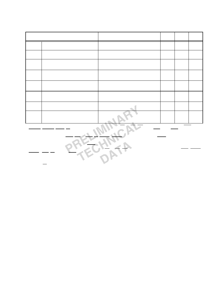
July 2000
ADSP-21161N Preliminary Data Sheet
For current information contact Analog Devices at (781) 461-3881
This information applies to a product under development. Its characteristics and specifications are subject to change with-
out notice. Analog Devices assumes no obligation regarding future manufacturing unless otherwise agreed to in writing.
26
REV. PrA
I
OZLA
Three-State Leakage Current
10
@ V
DDEXT
= max, V
IN
= 1.5 V
350
µA
I
OZLS
Three-State Leakage Current
6
@ V
DDEXT
= max, V
IN
= 0 V
150
µA
I
DD-
INPEAK
Supply Current (Internal)
11
t
CCLK
= 10.0 ns, V
DDINT
= max
TBD
mA
I
DD-
INHIGH
Supply Current (Internal)
12
t
CCLK
= 10.0 ns, V
DDINT
= max
TBD
mA
I
DD-
INLOW
Supply Current (Internal)
13
t
CCLK
= 10.0 ns, V
DDINT
= max
TBD
mA
I
DD-
IDLE
Supply Current (Idle)
14
V
DDINT
= max
TBD
mA
AI
DD
Supply Current (Analog)
15
@AV
DD
= max
10
mA
C
IN
Input Capacitance
16,17
f
IN
=1 MHz, T
CASE
=25°C,
V
IN
=1.8V
4.7
pF
1. Applies to output and bidirectional pins: DATA
47-16
, ADDR
23-0
, MS
3-0
, RD, WR, ACK, FLAG
11-0
, TIMEXP, HBG, REDY,
DMAG1, DMAG2, BR6-1, PA, BRST, LxDAT7-0, LxCLK, LxACK, SPICLK, MOSI, MISO, BMS, TDO, EMU.
2. See
"Output Drive Currents" on page 67
for typical drive current capabilities.
3. Applies to input pins: ACK, SBTS, IRQ
2-0
, HBR, CS, DMAR
1
, DMAR
2
, ID2-0, RPBA, EBOOT, SPIDS, LBOOT, CLKIN, RESET,
TCK.
4. Applies to input pins with internal pull-ups: TRST, TMS, TDI.
5. Applies to three-statable pins: DATA
47-16
, ADDR
24-0
, MS
3-0
, RD, WR, CLKOUT, ACK, FLAG
11-0
, REDY, HBG, DMAG
1
,
DMAG
2
, BMS, BR
6-1
, TDO, EMU. (Note that ACK is pulled up internally with 2 k
during reset in a multiprocessor system, when
ID2-0 = 001 and another ADSP-21161N is not requesting bus mastership.)
6. Applies to three-statable pins with internal pull-ups: DxA, DxB, SCLKx, SPICLK.
7. Applies to PA pin.
8. Applies to ACK pin when pulled up. (Note that ACK is pulled up internally with 2 k
during reset in a multiprocessor system, when
ID2-0 = 001 and another ADSP-21161N is not requesting bus mastership).
9. Applies to three-statable pins with internal pull-downs: LxDAT7-0, LxCLK, LxACK.
10.Applies to ACK pin when keeper latch enabled.
11.The test program used to measure I
DDINPEAK
represents worst case processor operation and is not sustainable under normal application
conditions. Actual internal power measurements made using typical applications are less than specified.
For more information, see
"Power Dissipation" on page 67.
12.I
DDINHIGH
is a composite average based on a range of high activity code.
For more information, see "Power Dissipation" on page 67.
13.I
DDINLOW
is a composite average based on a range of low activity code.
For more information, see "Power Dissipation" on page 67.
14.Idle denotes ADSP-21161N state during execution of IDLE instruction.
For more information, see "Power Dissipation" on page 67.
15.Characterized, but not tested.
16.Applies to all signal pins.
17.Guaranteed, but not tested.
Table 5 Electrical Characteristics (Continued)
Parameter
Test Conditions
Min
Max
Units
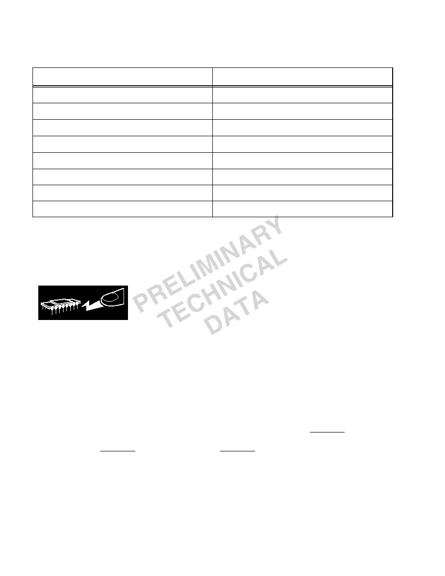
This information applies to a product under development. Its characteristics and specifications are subject to change with-
out notice. Analog Devices assumes no obligation regarding future manufacturing unless otherwise agreed to in writing.
ADSP-21161N Preliminary Data Sheet
July 2000
For current information contact Analog Devices at (781) 461-3881
27
REV. PrA
ESD Sensitivity
CAUTION: ESD (electrostatic discharge) sensitive device. Electrostatic
charges as high as 4000V readily accumulate on the human body and test
equipment and can discharge without detection. Although the
ADSP-21161N features proprietary ESD protection circuitry,
permanent damage may occur on devices subjected to high energy
electrostatic discharges. Therefore, proper ESD precautions are
recommended to avoid performance degradation or loss of functionality.
Timing Specifications
The ADSP-21161N's internal clock switches at higher frequencies than the system input clock
(CLKIN). To generate the internal clock, the DSP uses an internal phase-locked loop (PLL). This
PLL-based clocking minimizes the skew between the system clock (CLKIN) signal and the DSP's
internal clock (the clock source for the external port logic and I/O pads).
The ADSP-21161N's internal clock (a multiple of CLKIN) provides the clock signal for timing internal
memory, processor core, link ports, serial ports, and external port (as required for read/write strobes in
asynchronous access mode). During reset, program the ratio between the DSP's internal clock
frequency and external (CLKIN) clock frequency with the CLK_CFG1-0 and CLKDBL pins. Even
though the internal clock is the clock source for the external port, it is behaves as described on the Clock
Rate Ratio chart in CLKDBL pin description (see the CLKDBL description on
page 22
). To determine
switching frequencies for the serial and link ports, divide down the internal clock, using the
programmable divider control of each port (DIVx for the serial ports and LxCLKD1-0 for the link
ports).
Note the following definitions of various clock periods that are a function of CLKIN and the
appropriate ratio control.
Table 6 Absolute Maximum Ratings
1
Parameter
Absolute Maximum Rating
Internal (Core) Supply Voltage (V
DDINT
)
-0.3 V to +2.2 V
Analog (PLL) Supply Voltage (AV
DD
)
-0.3 V to +2.2 V
External (I/O) Supply Voltage (V
DDEXT
)
-0.3 V to +4.6 V
Input Voltage
-0.5 V to V
DDEXT
+ 0.5 V TBD
Output Voltage Swing
-0.5 V to V
DDEXT
+ 0.5 V TBD
Load Capacitance
200 pF
Storage Temperature Range
-65
°
C to +150
°
C
Lead Temperature (5 seconds)
+185
°
C
1. Stresses greater than those listed above may cause permanent damage to the device. These are stress ratings only, and functional oper-
ation of the device at these or any other conditions greater than those indicated in the operational sections of this specification is not
implied. Exposure to absolute maximum rating conditions for extended periods may affect device reliability.
W
A R NI NG
E S
D S
E N
S
I T I V E D E V I C
E
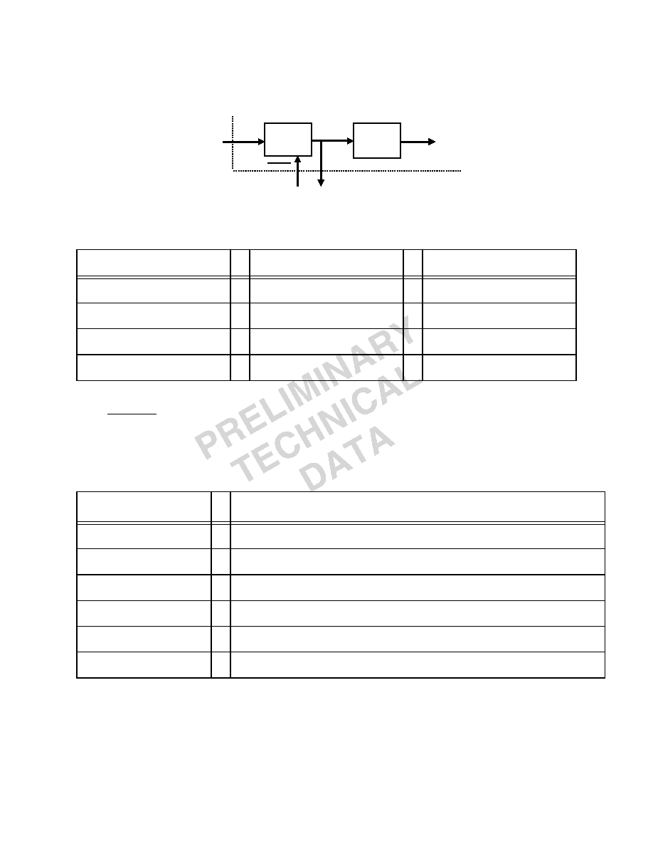
July 2000
ADSP-21161N Preliminary Data Sheet
For current information contact Analog Devices at (781) 461-3881
This information applies to a product under development. Its characteristics and specifications are subject to change with-
out notice. Analog Devices assumes no obligation regarding future manufacturing unless otherwise agreed to in writing.
28
REV. PrA
Figure 8, "Core Clock and System Clock Relationship to CLKIN"
allows Core-to-CLKIN ratios of 1:1,
2:1, 3:1, 4:1, 6:1, and 8:1 with external oscillator or crystal:
Figure 8 Core Clock and System Clock Relationship to CLKIN
Notes:
1. If CLKDBL is enabled (tied low at reset), then CLKOUT = PLLICLK = 2xCLKIN. Otherwise, CLK-
OUT = PLLICLK = CLKIN.
2. CCLK = Core Clock = PLLICLK x PLL Multiply Ratio (determined by CLK_CFG pins).
Table 8 Clock Relationships
Table 7 ADSP-21161N CLKOUT and CCLK Clock Generation Operation
Timing Requirements
Calculation
Description
CLKIN =
1/t
CKIN
=
Input
Clock
CLKOUT
=
1/t
TCK
=
External Port System Clock
PLLICLK
=
1/t
PLLIN
=
PLL Input Clock
CCLK
=
1/t
CCLK
=
Core Clock
Timing Requirements
Description
1
t
CK
=
CLKOUT Clock Period
t
CCLK
=
(Processor) Core Clock Period
t
LCLK
=
Link Port Clock Period = (t
CCLK
) * LR
t
SCLK
=
Serial Port Clock Period = (t
CCLK
) * SR
t
SDK
=
SDRAM Clock Period = (t
CCLK
) * SDCKR
t
SPICLK
=
SPI Clock Period = (t
CCLK
) * SPIR
CLKIN
CLKDBL
CLKOUT (EP System Clock Rate)
1x/2x Input
Clock Doubler
1:1, 2:1
Phase-Locked
Loop
2:1, 3:1, 4:1
CCLK
(Core Clock)
Tie to GND
to enable 2x
operation
PLLICLK
(PLL INPUT
CLOCK)
Crystal or
Clock
Oscillator

This information applies to a product under development. Its characteristics and specifications are subject to change with-
out notice. Analog Devices assumes no obligation regarding future manufacturing unless otherwise agreed to in writing.
ADSP-21161N Preliminary Data Sheet
July 2000
For current information contact Analog Devices at (781) 461-3881
29
REV. PrA
Use the exact timing information given. Do not attempt to derive parameters from the addition or
subtraction of others. While addition or subtraction would yield meaningful results for an individual
device, the values given in this data sheet reflect statistical variations and worst cases. Consequently, it
is not meaningful to add parameters to derive longer times.
See
Figure 37 on page 70
under Test Conditions for voltage reference levels.
Switching Characteristics specify how the processor changes its signals. Circuitry external to the
processor must be designed for compatibility with these signal characteristics. Switching characteristics
describe what the processor will do in a given circumstance. Use switching characteristics to ensure that
any timing requirement of a device connected to the processor (such as memory) is satisfied.
Timing Requirements apply to signals that are controlled by circuitry external to the processor, such as
the data input for a read operation. Timing requirements guarantee that the processor operates correctly
with other devices.
1. where:
LR = link port-to-core clock ratio (1, 2, 3, or 1:4, determined by LxCLKD)
SR = serial port-to-core clock ratio (wide range, determined by CLKDIV)
SDCKR = SDRAM-to-Core Clock Ratio (1:1 or 1:2, determined by SDCTL register)
SPIR = SPI-to-Core Clock Ratio (wide range, determined by SPICTL register)
LCLK = Link Port Clock
SCLK = Serial Port Clock
SDK = SDRAM Clock
SPICLK = SPI Clock
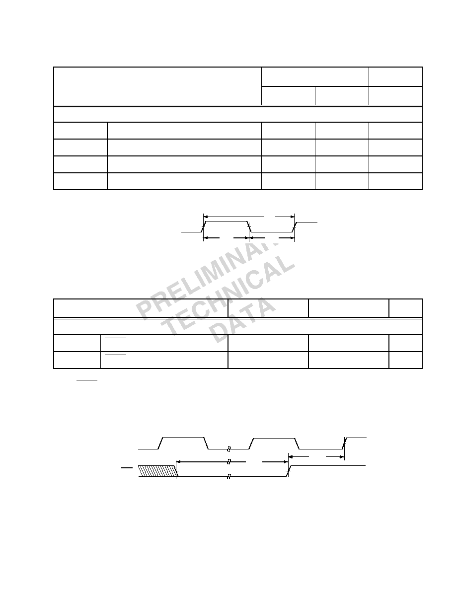
July 2000
ADSP-21161N Preliminary Data Sheet
For current information contact Analog Devices at (781) 461-3881
This information applies to a product under development. Its characteristics and specifications are subject to change with-
out notice. Analog Devices assumes no obligation regarding future manufacturing unless otherwise agreed to in writing.
30
REV. PrA
Figure 9 Clock Input
Figure 10 Reset
Table 9 Clock Input
Parameter
100 MHz
Min
Max
Units
Timing Requirements
t
CK
CLKIN Period
20
TBD
ns
t
CKL
CLKIN Width Low
8
40
ns
t
CKH
CLKIN Width High
8
40
ns
t
CKRF
CLKIN Rise/Fall (0.4V-2.0V)
3
ns
Table 10 Reset
Parameter
Min
Max
Units
Timing Requirements
t
WRST
RESET Pulse Width Low
1
1. Applies after the power-up sequence is complete. At power-up, the processor's internal phase-locked loop requires no more than 100
µ
s
while RESET is low, assuming stable VDD and CLKIN (not including start-up time of external clock oscillator).
4t
CK
ns
t
SRST
RESET Setup Before CLKIN High
2
2. Only required if multiple ADSP-21161Ns must come out of reset synchronous to CLKIN with program counters (PC) equal. Not
required for multiple ADSP-21161Ns communicating over the shared bus (through the external port), because the bus arbitration logic
synchronizes itself automatically after reset.
7.3
ns
C L K IN
t
C K H
t
C K
t
C K L
C LKIN
RESET
t
W RST
t
SRST
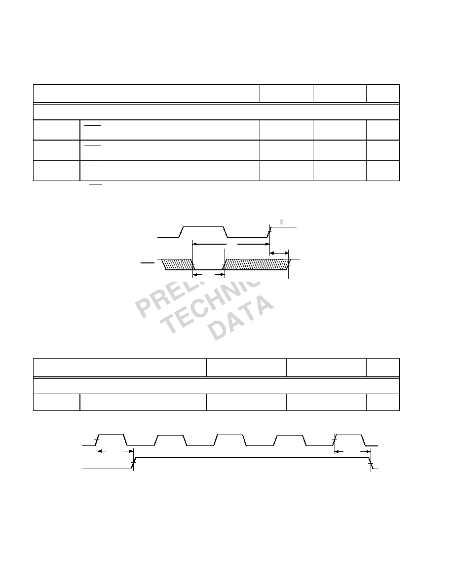
This information applies to a product under development. Its characteristics and specifications are subject to change with-
out notice. Analog Devices assumes no obligation regarding future manufacturing unless otherwise agreed to in writing.
ADSP-21161N Preliminary Data Sheet
July 2000
For current information contact Analog Devices at (781) 461-3881
31
REV. PrA
Figure 11 Interrupts
Timer
Figure 12 Timer
Table 11 Interrupts
Parameter
Min
Max
Units
Timing Requirements
t
SIR
IRQ
2-0
Setup Before CLKOUT High
1
1. Only required for IRQ
x
recognition in the following cycle.
8.3
ns
t
HIR
IRQ
2-0
Hold After CLKOUT High
1
-1.6
ns
t
IPW
IRQ
2-0
Pulse Width
2
2. Applies only if t
SIR
and t
HIR
requirements are not met.
2 + t
CK
ns
Table 12 Timer
Parameter
Min
Max Units
Switching Characteristic
t
DTEX
CLKOUT High to TIMEXP
-0.9
5.2
ns
C LKO UT
IRQ2-0
t
IPW
t
SIR
t
H IR
C LKO UT
TIM EX P
t
DTEX
t
DTEX
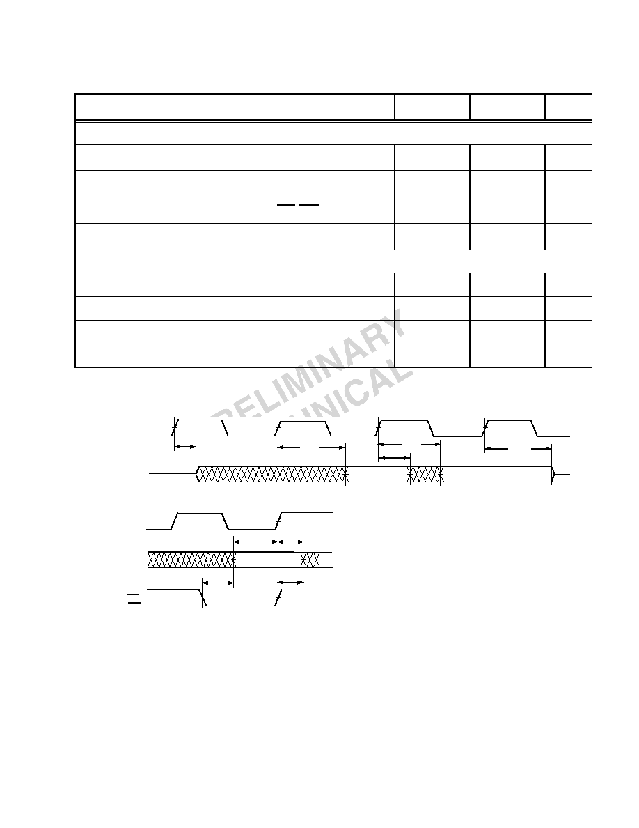
July 2000
ADSP-21161N Preliminary Data Sheet
For current information contact Analog Devices at (781) 461-3881
This information applies to a product under development. Its characteristics and specifications are subject to change with-
out notice. Analog Devices assumes no obligation regarding future manufacturing unless otherwise agreed to in writing.
32
REV. PrA
Figure 13 Flags
Table 13 Flags
Parameter
Min
Max
Units
Timing Requirement
t
SFI
FLAG11-0IN Setup Before CLKOUT High
1
6.3
ns
t
HFI
FLAG11-0IN Hold After CLKOUT High
1
-0.6
ns
t
DWRFI
FLAG11-0IN Delay After RD/WR Low
1
TBD
ns
t
HFIWR
FLAG11-0IN Hold After RD/WR Deasserted
1
TBD
ns
Switching Characteristics
t
DFO
FLAG11-0OUT Delay After CLKOUT High
7.2
ns
t
HFO
FLAG11-0OUT Hold After CLKOUT High
-0.9
ns
t
DFOE
CLKOUT High to FLAG11-0OUT Enable
-0.9
ns
t
DFOD
CLKOUT High to FLAG11-0OUT Disable
3.2
ns
1. Flag inputs meeting these setup and hold times for instruction cycle N will affect conditional instructions in instruction cycle N+2.
C LKO UT
FLA G 11-0OUT
FLA G O UTPUT
C LK O UT
RDX
,
WRX
FLA G IN PUT
FLA G 11-0IN
t
DFO
t
HFO
t
DFO
t
DF O D
t
DFO E
t
SFI
t
HFI
t
HFIW R
t
DW RFI
This information applies to a product under development. Its characteristics and specifications are subject to change with-
out notice. Analog Devices assumes no obligation regarding future manufacturing unless otherwise agreed to in writing.
ADSP-21161N Preliminary Data Sheet
July 2000
For current information contact Analog Devices at (781) 461-3881
33
REV. PrA
Memory Read--Bus Master
Use these specifications for asynchronous interfacing to memories (and memory-mapped peripherals)
without reference to CLKOUT. These specifications apply when the ADSP-21161N is the bus master
accessing external memory space in asynchronous access mode. Note that timing for ACK, DATA, RD,
WR, and DMAG strobe timing parameters only apply to asynchronous access mode.
Table 14 Memory Read--Bus Master
Parameter
Min
Max
Units
Timing Requirements:
t
DAD
Address, Selects Delay to Data
Valid
1,2
1. Data Delay/Setup: User must meet t
DAD
, t
DRLD
, or t
SDS.
2. The falling edge of MS
x
, BMS is referenced.
t
CK
.25t
CCLK
11+W
ns
t
DRLD
RD Low to Data Valid
1,3
3. Note that timing for ACK, DATA, RD, WR, and DMAG strobe timing parameters only apply to asynchronous access mode.
.75t
CK
11+W
ns
t
HDA
Data Hold from Address, Selects
4
0
ns
t
SDS
Data Setup to RD High
2
ns
t
HDRH
Data Hold from RD High
3,4
1
ns
t
DAAK
ACK Delay from Address,
Selects
2,5
t
CK
.5t
CCLK
12+W
ns
t
DSAK
ACK Delay from RD Low
3,5
t
CK
.75t
CCLK
11+W
ns
t
SAKC
ACK Setup to CLKOUT
3,5
.5t
CCLK
+5.3
ns
t
HAKC
ACK Hold After CLKOUT
3
-0.6
ns
Switching Characteristics
t
DRHA
Address Selects Hold After RD
High
3
.25t
CCLK
1+H
ns
t
DARL
Address Selects to RD Low
2
.25t
CCLK
1
ns
t
RW
RD Pulse Width
3
t
CK
.5t
CCLK
1+W
ns
t
RWR
RD High to WR, RD, DMAG
x
Low
3
.5t
CCLK
1+HI
ns
W = (number of wait states specified in WAIT register)
×
t
CK
.
HI = t
CK
(if an address hold cycle or bus idle cycle occurs, as specified in WAIT register; otherwise HI = 0).
H = t
CK
(if an address hold cycle occurs as specified in WAIT register; otherwise H = 0).
July 2000
ADSP-21161N Preliminary Data Sheet
For current information contact Analog Devices at (781) 461-3881
This information applies to a product under development. Its characteristics and specifications are subject to change with-
out notice. Analog Devices assumes no obligation regarding future manufacturing unless otherwise agreed to in writing.
34
REV. PrA
Figure 14 Memory Read--Bus Master
4. Data Hold: User must meet t
HDA
or t
HDRH
in asynchronous access mode. See
"Example System Hold Time Calculation" on page 69
for
the calculation of hold times given capacitive and dc loads.
5. ACK Delay/Setup: User must meet t
DAAK
, t
DSAK
, or t
SAKC
for deassertion of ACK (Low), all three specifications must be met for as-
sertion of ACK (High).
WR
,
DMAG
A C K
DA TA
RD
A DDRESS
MS
X,
BMS
t
DA RL
t
RW
t
DA D
t
DA A K
t
HDRH
t
HDA
t
RW R
t
DRLD
t
DRH A
t
DSA K
t
SDS
t
SAKC
t
HA KC
C LKO UT
This information applies to a product under development. Its characteristics and specifications are subject to change with-
out notice. Analog Devices assumes no obligation regarding future manufacturing unless otherwise agreed to in writing.
ADSP-21161N Preliminary Data Sheet
July 2000
For current information contact Analog Devices at (781) 461-3881
35
REV. PrA
Memory Write--Bus Master
Use these specifications for asynchronous interfacing to memories (and memory-mapped peripherals)
without reference to CLKOUT. These specifications apply when the ADSP-21161N is the bus master
accessing external memory space in asynchronous access mode. Note that timing for ACK, DATA, RD,
WR, and DMAG strobe timing parameters only apply to asynchronous access mode.
Table 15 Memory Write--Bus Master
Parameter
Min
Max
Units
Timing Requirements
t
DAAK
ACK Delay from Address,
Selects
1,2
t
CK
.5t
CCLK
12+W
ns
t
DSAK
ACK Delay from WR Low
1,3
t
CK
.75t
CCLK
11+W
ns
t
SAKC
ACK Setup to CLKOUT
1,3
.5t
CCLK
+5.3
ns
t
HAKC
ACK Hold After CLKOUT
1,3
-0.6
ns
Switching Characteristics
t
DAWH
Address Selects to WR
Deasserted
2,3
t
CK
.25t
CCLK
2+W
ns
t
DAWL
Address Selects to WR Low
2
.25t
CCLK
2
ns
t
WW
WR Pulse Width
3
t
CK
.5t
CCLK
1+W
ns
t
DDWH
Data Setup before WR High
3
t
CK
.25t
CCLK
12.5+W
ns
t
DWHA
Address Hold after WR
Deasserted
3
.25t
CCLK
1+H
ns
t
DWHD
Data Hold after WR Deasserted
3
.25t
CCLK
1+H
ns
t
DATRWH
Data Disable after WR
Deasserted
3,4
.25t
CCLK
1+H
.25t
CCLK
+2+H
ns
t
WWR
WR High to WR, RD, DMAGx
Low
3
.5t
CCLK
1+HI
ns
t
DDWR
Data Disable before WR or RD
Low
.25t
CCLK
1+I
ns
t
WDE
WR Low to Data Enabled
.25t
CCLK
1
ns
July 2000
ADSP-21161N Preliminary Data Sheet
For current information contact Analog Devices at (781) 461-3881
This information applies to a product under development. Its characteristics and specifications are subject to change with-
out notice. Analog Devices assumes no obligation regarding future manufacturing unless otherwise agreed to in writing.
36
REV. PrA
Figure 15 Memory Write--Bus Master
W = (number of wait states specified in WAIT register)
×
t
CK
.
H = t
CK
(if an address hold cycle occurs, as specified in WAIT register; otherwise H = 0).
HI = t
CK
(if an address hold cycle or bus idle cycle occurs, as specified in WAIT register; otherwise HI = 0).
I = t
CK
(if a bus idle cycle occurs, as specified in WAIT register; otherwise I = 0).
1. ACK Delay/Setup: User must meet t
DAAK
or t
DSAK
or t
SAKC
for deassertion of ACK (Low), all three specifications must be met for
assertion of ACK (High).
2. The falling edge of MS
x
, BMS is referenced.
3. Note that timing for ACK, DATA, RD, WR, and DMAG strobe timing parameters only apply to asynchronous access mode.
4. See
"Example System Hold Time Calculation" on page 69
for calculation of hold times given capacitive and dc loads.
Table 15 Memory Write--Bus Master
Parameter
Min
Max
Units
t
DA TRW H
RD
,
DMAG
A C K
DA TA
WR
A DDRESS
MS
X ,
BMS
t
DA W L
t
W W
t
DA A K
t
W W R
t
W DE
t
DDW R
t
DW HA
t
DA W H
t
DSA K
t
DDW H
t
DW HD
t
SAKC
t
HA KC
C LK O UT
This information applies to a product under development. Its characteristics and specifications are subject to change with-
out notice. Analog Devices assumes no obligation regarding future manufacturing unless otherwise agreed to in writing.
ADSP-21161N Preliminary Data Sheet
July 2000
For current information contact Analog Devices at (781) 461-3881
37
REV. PrA
Synchronous Read/Write--Bus Master
Use these specifications for interfacing to external memory systems that require CLKOUT, relative to
timing or for accessing a slave ADSP-21161N (in multiprocessor memory space). These synchronous
switching characteristics are also valid during asynchronous memory reads and writes except where
noted (see
"Memory Read--Bus Master" on page 33
and
"Memory Write--Bus Master" on page 35
).
When accessing a slave ADSP-21161N, these switching characteristics must meet the slave's timing
requirements for synchronous read/writes (see
"Synchronous Read/Write--Bus Slave" on page 39
). The
slave ADSP-21161N must also meet these (bus master) timing requirements for data and acknowledge
setup and hold times.
Table 16 Synchronous Read/Write--Bus Master
Parameter
Min
Max
Units
Timing Requirements
t
SSDATI
Data Setup Before CLKOUT
N
1
1. Note that timing for ACK, DATA, RD, WR, and DMAG strobe timing parameters only applies to synchronous access mode.
6.8
ns
t
HSDATI
Data Hold After CLKOUT
N
1
-0.6
ns
t
SACKC
ACK Setup Before CLKOUT
N
1
.5t
CCLK
+5.3
ns
t
HACKC
ACK Hold After CLKOUT
N
1
-0.6
ns
Switching Characteristics
t
DADDO
Address, MSx, BMS, BRST, Delay After CLKIN
8.2
ns
t
HADDO
Address, MSx, BMS, BRST, Hold After CLKIN
-0.4
ns
t
DRDO
RD High Delay After CLKOUT
N
1
.25t
CCLK
2.9
.25t
CCLK
+7.2
ns
t
DWRO
WR High Delay After CLKOUT
N
1
.25t
CCLK
2.9
.25t
CCLK
+7.2
ns
t
DRWL
RD/WR Low Delay After CLKOUT
.25t
CCLK
2.9
.25t
CCLK
+7.2
ns
t
DDATO
Data Delay After CLKOUT
10.7
ns
t
HDATO
Data Hold After CLKOUT
-0.4
ns
t
DACKMO
ACK Delay After CLKOUT
N
2
2. Applies to broadcast write, master precharge of ACK.
.25t
CCLK
+1.1
.25t
CCLK
+7.2
ns
t
ACKMTR
ACK Disable Before CLKOUT
N
2
.25t
CCLK
4.9
ns
t
DCKOO
CLKOUT Delay After CLKIN
1.6
2.3
ns
t
CKOP
CLKOUT Period
t
CK
t
CK
3
3. Applies only when the DSP drives a bus operation; CLKOUT held inactive or three-state otherwise, For more information, see the
System Design chapter in the ADSP-21160 or ADSP-21161N SHARC DSP Technical Reference.
ns
t
CKWH
CLKOUT Width High
t
CK
/2 - 2
t
CK
/2 + 2
3
ns
t
CKWL
CLKOUT Width Low
t
CK
/2 - 2
t
CK
/2 + 2
3
ns
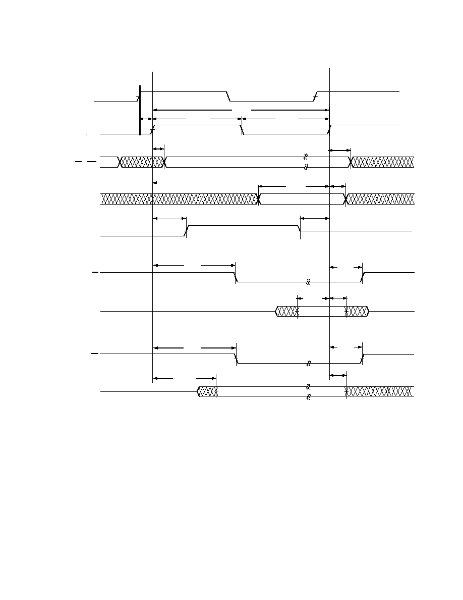
July 2000
ADSP-21161N Preliminary Data Sheet
For current information contact Analog Devices at (781) 461-3881
This information applies to a product under development. Its characteristics and specifications are subject to change with-
out notice. Analog Devices assumes no obligation regarding future manufacturing unless otherwise agreed to in writing.
38
REV. PrA
Figure 16 Synchronous Read/Write--Bus Master
t
DC KO O
t
C KO P
t
C KW L
t
C KW H
C LKIN
C LKO UT
A DDRESS
MS
X,
BRST
t
HA DDO
t
DA DD O
A C K
(IN )
RD
DA TA
(O UT)
WR
DA TA
(IN )
W RITE C Y C LE
REA D C Y C LE
t
DRW L
t
HSDATI
t
SSDATI
t
DRDO
t
DW RO
t
HDATO
t
DDATO
t
DRW L
t
SAC K C
t
HA C KC
A C K
(O UT)
t
DA C KM O
t
A C KM TR
This information applies to a product under development. Its characteristics and specifications are subject to change with-
out notice. Analog Devices assumes no obligation regarding future manufacturing unless otherwise agreed to in writing.
ADSP-21161N Preliminary Data Sheet
July 2000
For current information contact Analog Devices at (781) 461-3881
39
REV. PrA
Synchronous Read/Write--Bus Slave
Use these specifications for ADSP-21161N bus master accesses of a slave's IOP registers in
multiprocessor memory space. The bus master must meet these (bus slave) timing requirements.
Table 17 Synchronous Read/Write--Bus Slave
Parameter
Min
Max
Units
Timing Requirements:
t
SADDI
Address, BRST Setup Before CLKOUT
7.3
ns
t
HADDI
Address, BRST Hold After CLKOUT
-0.6
ns
t
SRWI
RD/WR Setup Before CLKOUT
7.3
ns
t
HRWI
RD/WR Hold After CLKOUT
-0.6
ns
t
SSDATI
Data Setup Before CLKOUT
6.8
ns
t
HSDATI
Data Hold After CLKOUT
-0.6
ns
Switching Characteristics
t
DDATO
Data Delay After CLKOUT
10.7
ns
t
HDATO
Data Hold After CLKOUT
-0.4
ns
t
DACKC
ACK Delay After CLKOUT
8.2
ns
t
HACKO
ACK Hold After CLKOUT
-0.4
ns
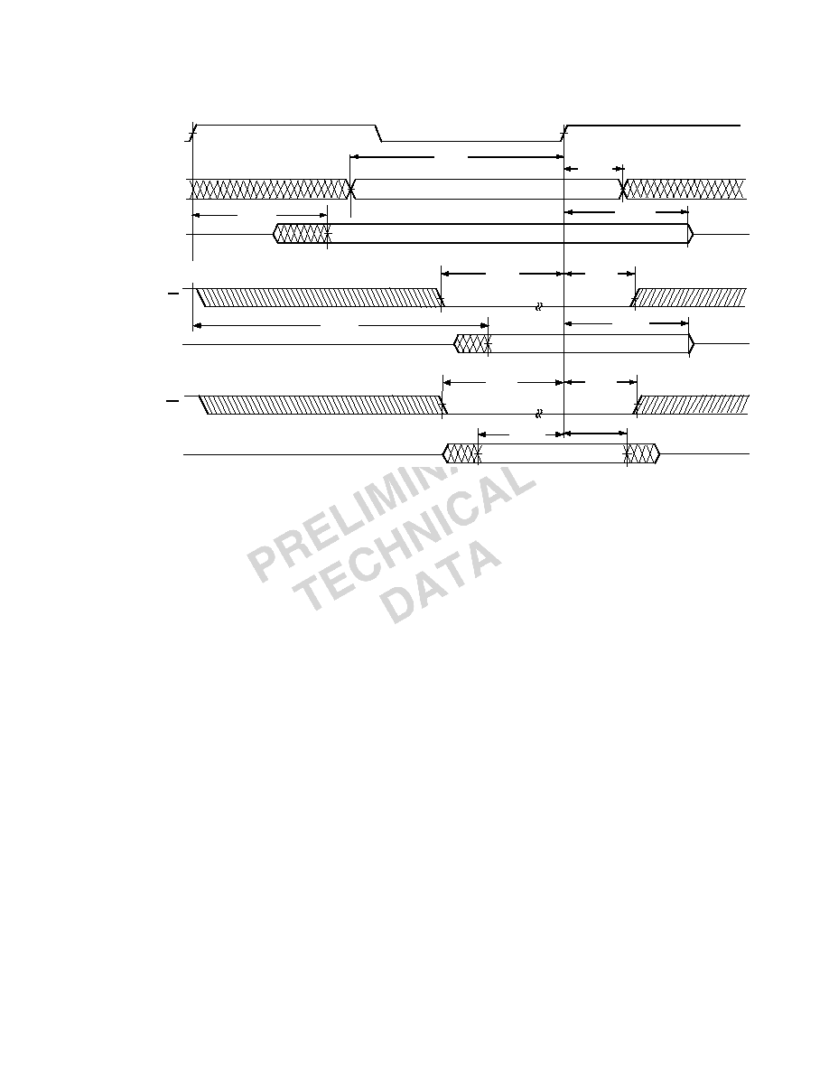
July 2000
ADSP-21161N Preliminary Data Sheet
For current information contact Analog Devices at (781) 461-3881
This information applies to a product under development. Its characteristics and specifications are subject to change with-
out notice. Analog Devices assumes no obligation regarding future manufacturing unless otherwise agreed to in writing.
40
REV. PrA
Figure 17 Synchronous Read/Write--Bus Slave
C LK O UT
A DDRESS
A C K
RD
DA TA
(O UT)
WR
W RITE A C C ESS
DA TA
(IN)
REA D A C C ESS
t
SADDI
t
HA DDI
t
DA C KC
t
HA C KO
t
HRW I
t
SRW I
t
DDATO
t
HDATO
t
SRW I
t
HRW I
t
HSDA TI
t
SSDATI
This information applies to a product under development. Its characteristics and specifications are subject to change with-
out notice. Analog Devices assumes no obligation regarding future manufacturing unless otherwise agreed to in writing.
ADSP-21161N Preliminary Data Sheet
July 2000
For current information contact Analog Devices at (781) 461-3881
41
REV. PrA
Multiprocessor Bus Request and Host Bus Request
Use these specifications for passing of bus mastership between multiprocessing ADSP-21161Ns (BRx)
or a host processor (HBR, HBG).
Table 18 Multiprocessor Bus Request and Host Bus Request
Parameter
Min
Max
Units
Timing Requirements:
t
HBGRCSV
HBG Low to RD/WR/CS Valid
1
TBD
TBD
ns
t
SHBRI
HBR Setup Before CLKOUT
N
2
8.3
ns
t
HHBRI
HBR Hold After CLKOUT
N
2
-0.6
ns
t
SHBGI
HBG Setup Before CLKOUT
N
8.3
ns
t
HHBGI
HBG Hold After CLKOUT High
-0.6
ns
t
SBRI
BR
x
, PA Setup Before CLKOUT
N
11.3
ns
t
HBRI
BR
x
, PA Hold After CLKOUT High
-0.6
ns
t
SPAI
PA Setup Before CLKOUT
N
11.3
ns
t
HPAI
PA Hold After CLKOUT High
-0.6
ns
t
SRPBAI
RPBA Setup Before CLKOUT
N
8.3
ns
t
HRPBAI
RPBA Hold After CLKOUT
N
0.4
ns
Switching Characteristics
t
DHBGO
HBG Delay After CLKOUT
TBD
ns
t
HHBGO
HBG Hold After CLKOUT
TBD
ns
t
DBRO
BRx Delay After CLKOUT
7.2
ns
t
HBRO
BR
x
Hold After CLKOUT
-0.4
ns
t
DPASO
PA Delay After CLKOUT, Slave
7.2
ns
t
TRPAS
PA Disable After CLKOUT, Slave
-0.4
ns
t
DPAMO
PA Delay After CLKOUT, Master
.25t
CCLK
+7.2
ns
t
PATR
PA Disable Before CLKOUT, Master
.25t
CCLK
+0.6
ns
t
DRDYCS
REDY (O/D) or (A/D) Low from CS and HBR
Low
3
TBD
ns
t
TRDYHG
REDY (O/D) Disable or REDY (A/D) High from
HBG
3
TBD
ns
See note on
page 42
.
July 2000
ADSP-21161N Preliminary Data Sheet
For current information contact Analog Devices at (781) 461-3881
This information applies to a product under development. Its characteristics and specifications are subject to change with-
out notice. Analog Devices assumes no obligation regarding future manufacturing unless otherwise agreed to in writing.
42
REV. PrA
t
ARDYTR
REDY (A/D) Disable from CS or HBR High
3
TBD
ns
1. For first asynchronous access after HBR and CS asserted, ADDR
23-0
must be a non-MMS value (TBD) before RD or WR goes low or
by t
HBGRCSV
after HBG goes low. This is easily accomplished by driving an upper address signal high when HBG is asserted.
2. Only required for recognition in the current cycle.
3. (O/D) = open drain, (A/D) = active drive.
Table 18 Multiprocessor Bus Request and Host Bus Request
Parameter
Min
Max
Units
See note on
page 42
.
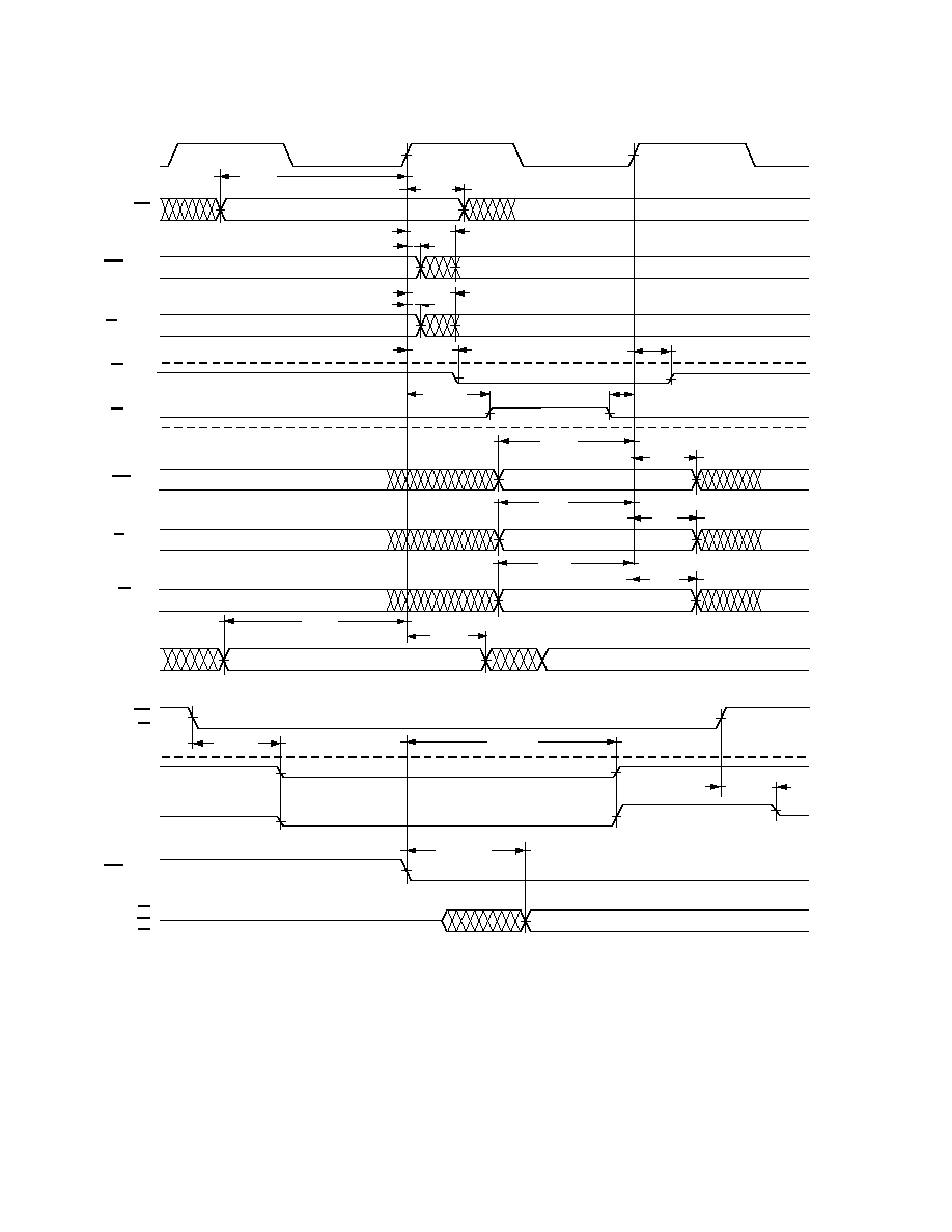
This information applies to a product under development. Its characteristics and specifications are subject to change with-
out notice. Analog Devices assumes no obligation regarding future manufacturing unless otherwise agreed to in writing.
ADSP-21161N Preliminary Data Sheet
July 2000
For current information contact Analog Devices at (781) 461-3881
43
REV. PrA
Figure 18 Multiprocessor Bus Request and Host Bus Request
BR
X (IN )
t
HBRI
HBR
CS
RPBA
REDY
(O /D)
REDY
(A/D)
HBG
(O UT)
RD
WR
CS
O /D = O PEN DRA IN, A /D = AC TIVE DRIVE
t
HRPBA I
t
SRPBA I
t
DRDYC S
t
HBG RC SV
t
TRDYHG
t
A RDYTR
HBG
(IN )
t
SHBG I
t
HH BG I
t
SBRI
C LKO UT
HBR
HBG
(O UT)
BR
X (O UT)
PA
(O U T)
(SLA VE)
t
HH BRI
t
SHBRI
t
HH BG O
t
DH BG O
t
DBRO
t
HBRO
t
DPASO
t
TRPA S
PA
(O U T)
(M A STER)
t
DPAM O
t
PA TR
PA
(IN )
(O /D)
t
HPAI
t
SPAI
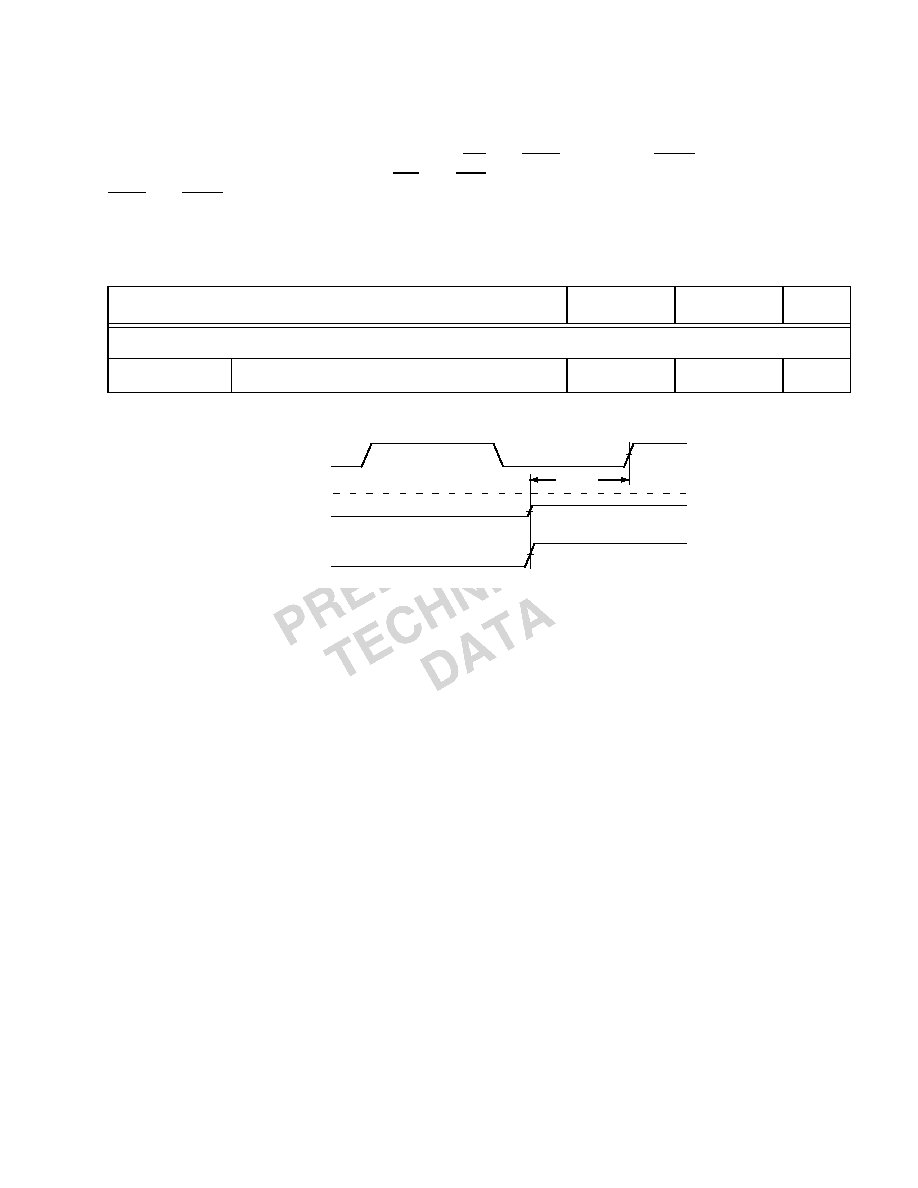
July 2000
ADSP-21161N Preliminary Data Sheet
For current information contact Analog Devices at (781) 461-3881
This information applies to a product under development. Its characteristics and specifications are subject to change with-
out notice. Analog Devices assumes no obligation regarding future manufacturing unless otherwise agreed to in writing.
44
REV. PrA
Asynchronous Read/Write--Host to ADSP-21161N
Use these specifications (continued on
page 45
and
page 46
) for asynchronous host processor accesses
of an ADSP-21161N, after the host has asserted CS and HBR (low). After HBG is returned by the
ADSP-21161N, the host can drive the RD and WR pins to access the ADSP-21161N's IOP register.
HBR and HBG are assumed low for this timing.
Note: Host internal memory access is not supported.
Figure 19 Synchronous REDY Timing
Table 19 Write Cycle (Synchronous REDY)
Parameter
Min
Max
Units
Switching Characteristics
t
SRDYCK
REDY (O/D) or (A/D) Disable to CLKOUT
TBD
TBD
ns
C LKIO UT
REDY (O /D)
O /D = O PEN DRAIN , A/D = AC TIVE DRIVE
t
SRDYC K
REDY (A/D)
This information applies to a product under development. Its characteristics and specifications are subject to change with-
out notice. Analog Devices assumes no obligation regarding future manufacturing unless otherwise agreed to in writing.
ADSP-21161N Preliminary Data Sheet
July 2000
For current information contact Analog Devices at (781) 461-3881
45
REV. PrA
Table 20 Read Cycle
Parameter
Min
Max
Units
Timing Requirements
t
SADRDL
Address Setup CS Low Before RD Low
1
0
ns
t
HADRDH
Address Hold CS Hold Low After RD
0
ns
t
WRWH
RD/WR High Width
5
ns
t
DRDHRDY
RD High Delay After REDY (O/D) Disable
0
ns
t
DRDHRDY
RD High Delay After REDY (A/D) Disable
0
ns
Switching Characteristics
t
SDATRDY
Data Valid Before REDY Disable from Low
2
ns
t
DRDYRDL
REDY (O/D) or (A/D) Low Delay After RD Low
10
ns
t
RDYPRD
REDY (O/D) or (A/D) Low Pulse Width for
Read
2t
CK
ns
t
HDARWH
Data Disable After RD High
2
TBD
ns
1. Not required if RD and address are valid t
HBGRCSV
after HBG goes low. For first access after HBR asserted, ADDR
23-0
must be a
non-MMS value (TBD) before RD or WR goes low or by t
HBGRCSV
after HBG goes low. This is easily accomplished by driving an
upper address signal high when HBG is asserted.
REDY (O /D)
RD
REA D C Y C LE
A DDRESS/
CS
DA TA (O U T)
REDY (A /D)
t
SADRDL
t
DRDYRDL
t
W RW H
t
HA DRDH
t
HDARW H
t
RDY PRD
t
DRDHRDY
t
SDA TRDY
Figure 20 Asynchronous Read--Host to ADSP-21161N
July 2000
ADSP-21161N Preliminary Data Sheet
For current information contact Analog Devices at (781) 461-3881
This information applies to a product under development. Its characteristics and specifications are subject to change with-
out notice. Analog Devices assumes no obligation regarding future manufacturing unless otherwise agreed to in writing.
46
REV. PrA
Table 21 Write Cycle
Parameter
Min
Max
Units
Timing Requirements
t
SCSWRL
CS Low Setup Before WR Low
0
ns
t
HCSWRH
CS Low Hold After WR High
0
ns
t
SADWRH
Address Setup Before WR High
5
ns
t
HADWRH
Address Hold After WR High
2
ns
t
WWRL
WR Low Width
7
ns
t
WRWH
RD/WR High Width
5
ns
t
DWRHRDY
WR High Delay After REDY (O/D) or (A/D) Disable
0
ns
t
SDATWH
Data Setup Before WR High
5
ns
t
HDATWH
Data Hold After WR High
1
ns
Switching Characteristics
t
DRDYWRL
REDY (O/D) or (A/D) Low Delay After WR/CS Low
10
ns
t
RDYPWR
REDY (O/D) or (A/D) Low Pulse Width for Write
TBD
ns
O /D = O PEN DRAIN , A /D = AC TIVE DRIVE
REDY (O /D)
WR
W RITE C Y C LE
DA TA (IN)
A DDRESS
REDY (A/D)
CS
t
SDA TW H
t
HDATW H
t
W W RL
t
DRDYW RL
t
W RW H
t
HA DW RH
t
RDYPW R
t
DW RHRDY
t
SADW RH
t
SC SW RL
t
HC SW RH
Figure 21 Asynchronous Write--Host to ADSP-21161N
This information applies to a product under development. Its characteristics and specifications are subject to change with-
out notice. Analog Devices assumes no obligation regarding future manufacturing unless otherwise agreed to in writing.
ADSP-21161N Preliminary Data Sheet
July 2000
For current information contact Analog Devices at (781) 461-3881
47
REV. PrA
Three-State Timing--Bus Master, Bus Slave, HBR, SBTS
These specifications show how the memory interface is disabled (stops driving) or enabled (resumes
driving) relative to CLKOUT and the SBTS pin. This timing is applicable to bus master transition
cycles (BTC) and host transition cycles (HTC) as well as the SBTS pin.
Table 22 Three-State Timing--Bus Slave, HBR, SBTS
Parameter
Min
Max
Units
Timing Requirements
t
STSCK
SBTS Setup Before CLKOUT
8.3
ns
t
HTSCK
SBTS
Hold After CLKOUT
-0.6
ns
Switching Characteristics
t
MIENA
Address/Select Enable After CLKOUT
-0.4
7.2
ns
t
MIENS
Strobes Enable After CLKOUT
1
1. Strobes = RD, WR, DMAGx.
-0.4
3.2
ns
t
MIENHG
HBG Enable After CLKOUT
-0.4
7.2
ns
t
MITRA
Address/Select Disable After CLKOUT
.5t
CK
-0.9
.5t
CK
+3.2
ns
t
MITRS
Strobes Disable After CLKOUT
1
t
CK
.25t
CCLK
-1.9
t
CK
.25t
CCLK
+3.2
ns
t
MITRHG
HBG Disable After CLKOUT
-0.4
3.2
ns
t
DATEN
Data Enable After CLKOUT
N
2
2. In addition to bus master transition cycles, these specs also apply to bus master and bus slave synchronous read/write.
-0.4
7.2
ns
t
DATTR
Data Disable After CLKOUT
2
-0.4
3.2
ns
t
ACKEN
ACK Enable After CLKOUT
2
-0.4
7.2
ns
t
ACKTR
ACK Disable After CLKOUT
2
1.5
5
ns
t
CDCEN
CLKOUT Enable After CLKIN
-0.4
7.2
ns
t
CDCTR
CLKOUT Disable After CLKIN
.5t
CK
-0.9
.5t
CK
+3.2
ns
t
MTRHBG
Memory Interface Disable Before HBG
Low
3
3. Memory Interface = Address, RD, WR, MSx, DMAG
x
, BMS (in EPROM boot mode).
.5t
CK
4
TBD
ns
t
MENHBG
Memory Interface Enable After HBG
High
3
t
CK
5
TBD
ns
July 2000
ADSP-21161N Preliminary Data Sheet
For current information contact Analog Devices at (781) 461-3881
This information applies to a product under development. Its characteristics and specifications are subject to change with-
out notice. Analog Devices assumes no obligation regarding future manufacturing unless otherwise agreed to in writing.
48
REV. PrA
Figure 22 Three-State Timing
DMA Handshake
These specifications describe the three DMA handshake modes. In all three modes DMAR is used to
initiate transfers. For handshake mode, DMAG controls the latching or enabling of data externally. For
external handshake mode, the data transfer is controlled by the ADDR
24-0
, RD, WR, MS
3-0
, ACK, and
DMAG signals. For Paced Master mode, the data transfer is controlled by ADDR
24-0
, RD, WR, MS
3-0
,
and ACK (not DMAG). For Paced Master mode, the Memory Read-Bus Master, Memory Write-Bus
Master, and Synchronous Read/Write-Bus Master timing specifications for ADDR
23-0
, RD, WR,
MS3-0, DATA
47-16
, and ACK also apply.
Table 23 DMA Handshake
Parameter
Min
Max
Units
Timing Requirements
t
SDRC
DMARx Setup Before CLKOUT
N
1
5.3
ns
t
WDR
DMARx Width Low (Nonsynchronous)
.5t
CK
+1
ns
t
SDATDGL
Data Setup After DMAGx Low
2
.75t
CK
7
ns
t
HDATIDG
Data Hold After DMAGx High
2
ns
C L K O U T
SBTS
A C K
M E M O R Y
IN T E R F A C E
t
M T R H B G
HBG
M E M O R Y IN TE R F A C E = A D D R E S S ,
RD
,
W R
,
M S
X ,
HBG
,
DM AG
X .
BM S
( IN E P R O M B O O T M O D E )
C L K O U T
t
M E N H B G
t
C D C T R
D A T A
M E M O R Y
IN T E R F A C E
t
M IT R A ,
t
M IT R S ,
t
M IT R H G
t
S T S C K
t
H T S C K
t
D A T T R
t
D A T E N
t
A C K T R
t
A C K E N
t
C D C E N
t
M IE N A ,
t
M IE N S ,
t
M IE N H G
C L K IN
This information applies to a product under development. Its characteristics and specifications are subject to change with-
out notice. Analog Devices assumes no obligation regarding future manufacturing unless otherwise agreed to in writing.
ADSP-21161N Preliminary Data Sheet
July 2000
For current information contact Analog Devices at (781) 461-3881
49
REV. PrA
t
DATDRH
Data Valid After DMAR
x
High
2
TBD
ns
t
DMARLL
DMAR
x
Low Edge to Low Edge
3
t
CK
ns
t
DMARH
DMAR
x
Width High
.5t
CK
+1
ns
Switching Characteristics
t
DDGL
DMAG
x
Low Delay After CLKOUT
.25t
CCLK
-0.9
.25t
CCLK
+7.2
ns
t
WDGH
DMAG
x
High Width
.5t
CCLK
1+HI
ns
t
WDGL
DMAG
x
Low Width
t
CK
.5t
CCLK
1
ns
t
HDGC
DMAG
x
High Delay After CLKOUT
t
CK
.25t
CCLK
-0.4
t
CK
.25t
CCLK
+7.2
ns
t
VDATDGH
Data Valid Before DMAG
x
High
4
t
CK
.25t
CCLK
8
t
CK
.25t
CCLK
+5
ns
t
DATRDGH
Data Disable After DMAG
x
High
5
.25t
CCLK
+1.5
.25t
CCLK
+1.5
ns
t
DGWRL
WR Low Before DMAG
x
Low
1
1
ns
t
DGWRH
DMAG
x
Low Before WR High
t
CK
.5t
CCLK
2+W
ns
t
DGWRR
WR High Before DMAG
x
High
6
1
1
ns
t
DGRDL
RD Low Before DMAG
x
Low
1
1
ns
t
DRDGH
RD Low Before DMAG
x
High
t
CK
.5t
CCLK
2+W
ns
t
DGRDR
RD High Before DMAG
x
High
6
1
1
ns
t
DGWR
DMAR
x
High to WR, RD, DMAG
x
Low
.5t
CCLK
1+HI
ns
t
DADGH
Address/Select Valid to DMAG
x
High
TBD
ns
t
DDGHA
Address/Select Hold after DMAG
x
High
TBD
ns
W = (number of wait states specified in WAIT register) × t
CK
.
HI = t
CK
(if data bus idle cycle occurs, as specified in WAIT register; otherwise HI = 0).
1. Only required for recognition in the current cycle.
2. t
SDATDGL
is the data setup requirement if DMAR
x
is not being used to hold off completion of a write. Otherwise, if DMAR
x
low holds
off completion of the write, the data can be driven t
DATDRH
after DMAR
x
is brought high.
Table 23 DMA Handshake (Continued)
Parameter
Min
Max
Units
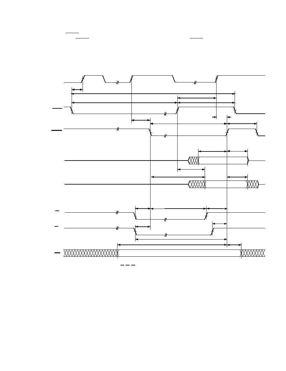
July 2000
ADSP-21161N Preliminary Data Sheet
For current information contact Analog Devices at (781) 461-3881
This information applies to a product under development. Its characteristics and specifications are subject to change with-
out notice. Analog Devices assumes no obligation regarding future manufacturing unless otherwise agreed to in writing.
50
REV. PrA
Figure 23 DMA Handshake Timing
3. Use t
DMARLL
if DMAR
x
transitions synchronous with CLKOUT. Otherwise, use t
WDR
and t
DMARH
.
4. t
VDATDGH
is valid if DMAR
x
is not being used to hold off completion of a read. If DMAR
x
is used to prolong the read, then
t
VDATDGH
= t
CK
.25t
CCLK
8 + (n
×
t
CK
) where n equals the number of extra cycles that the access is prolonged.
5. See
"Example System Hold Time Calculation" on page 69
for calculation of hold times given capacitive and dc loads.
6. This parameter applies for synchronous access mode only.
C LKO UT
t
SDRC
DMARX
DA TA
DATA
RD
WR
t
W DR
t
SDRC
t
DM ARH
t
DM ARLL
t
HDG C
t
W DG H
t
DDG L
DMAGX
t
VDATD G H
t
DA TDRH
t
DA TRDG H
t
HDATIDG
t
DG W RL
t
DG W RH
t
DG W RR
t
DG RDL
t
DRDG H
t
DG RDR
t
SDA TDG
L
* M EM O RY READ BUS MA STER, M EM O RY W RITE BUS M ASTER, O R SYN C HRO N OUS REA D/W RITE BUS M A STER
TIM IN G SPECIFIC ATIO N S FO R ADDR23-0,
RD
,
WR
,
MS3-0
A ND AC K ALSO A PPLY H ERE.
(EX TERN A L DEVIC E TO EXTERNAL M EM O RY )
(EX TERN A L M EM O RY TO EX TERNA L DEVIC E)
TRA N SFERS BETW EEN A D SP -211 61N
IN TERN A L M EM O RY A N D EX TERN A L D EV IC E
TRA N SFERS BETW EEN EX TERN A L D EV IC E A N D
EX TERN A L M EMO RY *
(EX TERN A L HA NDSH AKE M O DE)
t
DDG H A
A DDRESS
MSX
,
t
DA DG H
t
W DG L
(FRO M EX TERN A L DRIVE TO ADSP-21161N)
(FRO M ADSP-2116X TO EX TERN A L DRIVE)
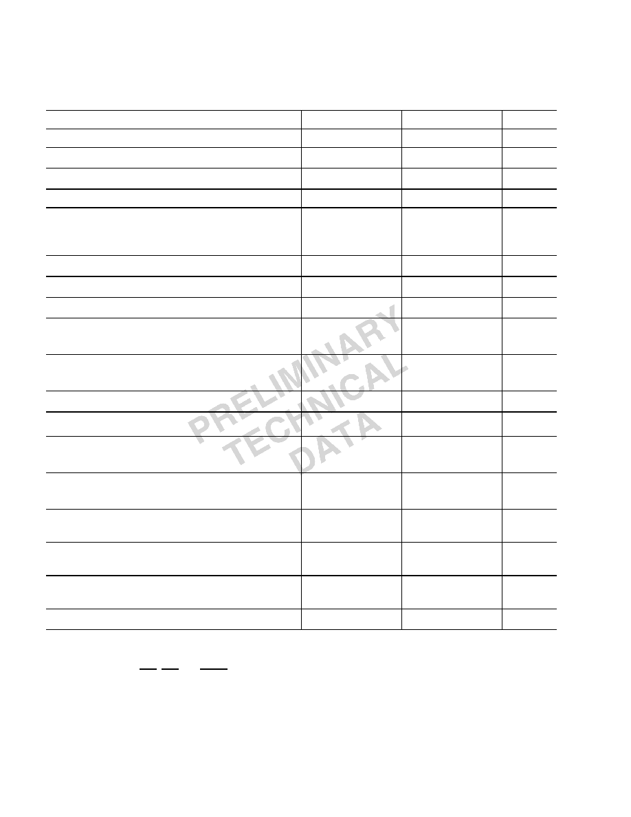
This information applies to a product under development. Its characteristics and specifications are subject to change with-
out notice. Analog Devices assumes no obligation regarding future manufacturing unless otherwise agreed to in writing.
ADSP-21161N Preliminary Data Sheet
July 2000
For current information contact Analog Devices at (781) 461-3881
51
REV. PrA
SDRAM Interface Bus Master
Use these specifications for ADSP-21161N bus master accesses of SDRAM:
Parameter
Min
Max
Units
Timing Requirements:
t
SDSDK
Data Setup before SDCLK
2.0
ns
t
HDSDK
Data Hold after SDCLK
1.5
ns
Switching Characteristics:
t
DSDK1
First SDCLK Rise Delay after
CLKOUT
1, 2
1. For the second, third, and forth rising edges of SDCLK delay from CLKOUT, add appropriate number of SDCLK period to the
t
DSDK1
and t
SSDKC1
values, depending upon the SDCKR value and the Core clk to CLKOUT ratio.
2. SDCKR = 1 for SDCLK equal to core clock frequency and SDCKR = 2 for SDCLK equal to half core clock frequency.
3.Command = SDCKE, RAS, CAS, and SDWE.
4. SDRAM Controller adds one SDRAM CLK three-stated cycle delay on a read followed, by a write.
SDCKR x t
CCLK
-0.25 x t
CCLK
-
0.4
SDCKR x t
CCLK
-0.25 x t
CCLK
+
1.7
ns
t
SDK
SDCLK Period
10.0
2 x t
CCLK
ns
t
SDKH
SDCLK Width High
4.0
ns
t
SDKL
SDCLK Width Low
4.0
ns
t
DCADSDK
Command, Address, Data,
Delay after SDCLK
3
.25 x t
CCLK
+ 2.0
ns
t
HCADSDK
Command, Address, Data,
Hold after SDCLK
3
1.3
ns
t
SDTRSDK
Data Three-State after SDCLK
0.5 x t
CCLK
+ 2.0
ns
t
SDENSDK
Data Enable After SDCLK
4
0.75 x t
CCLK
ns
t
SDCTR
Command Three-State After
CLKOUT
3
0.5 x t
CCLK
- 0.4
0.5 x t
CCLK
+ 1.7
ns
t
SDCEN
Command Enable
After CLKOUT
3
-0.4
1.7
ns
t
SDSDKTR
SDCLK Three-State after
CLKOUT
-0.4
1.7
ns
t
SDSDKEN
SDCLK Enable after
CLKOUT
-0.4
1.7
ns
t
SDATR
Address Three-State after
CLKOUT
0.5 x t
CK
- 0.9
0.5 x t
CK
+ 3.2
ns
t
SDAEN
Address Enable after CLKOUT -0.4
7.2
ns
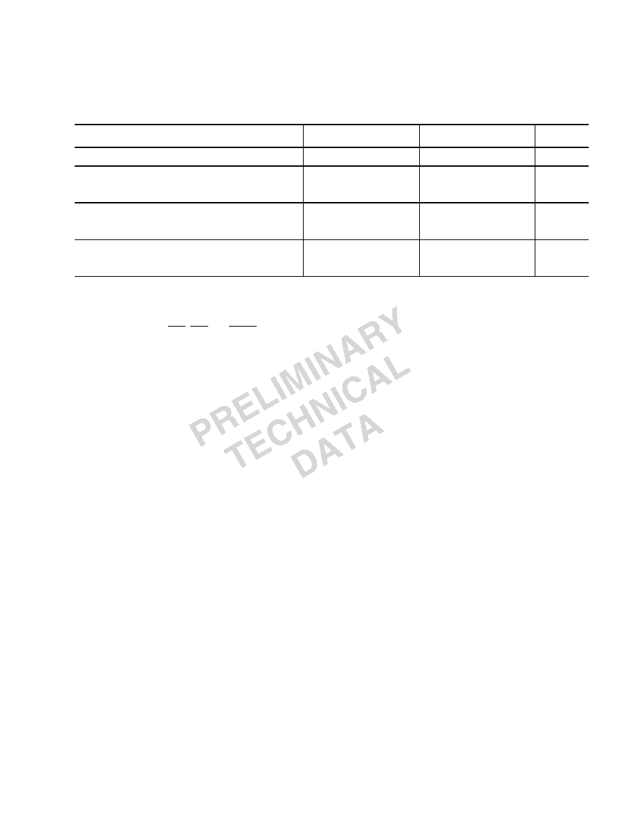
July 2000
ADSP-21161N Preliminary Data Sheet
For current information contact Analog Devices at (781) 461-3881
This information applies to a product under development. Its characteristics and specifications are subject to change with-
out notice. Analog Devices assumes no obligation regarding future manufacturing unless otherwise agreed to in writing.
52
REV. PrA
SDRAM Interface Bus Slave
These timing requirements allow a bus slave to sample the bus master's SDRAM command and detect
when a refresh occurs.
NOTES
1. For the second, third, and forth rising edges of SDCLK delay from CLKOUT, add appropriate number of SDCLK period to the
t
DSDK1
and t
SSDKC1
values, depending upon the SDCKR value and the Core clk to CLKOUT ratio.
2. SDCKR = 1 for SDCLK equal to core clock frequency and SDCKR = 2 for SDCLK equal to half core clock frequency.
3.Command = SDCKE, RAS, CAS, and SDWE.
Parameter
Min
Max
Unit
Timing Requirements:
t
SSDKC1
First SDCLK Rise After
CLKOUT
1, 2
SDCKR x tCCLK
-0.5 x t
CCLK
-1.4
SDCKR x tCCLK
-0.25 x t
CCLK
+ 2.7
ns
t
SCSDK
Command Setup Before
SDCLK
3
0.0
ns
t
HCSDK
Command Hold After
SDCLK
3
2.0
ns
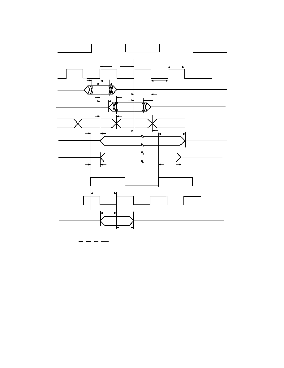
This information applies to a product under development. Its characteristics and specifications are subject to change with-
out notice. Analog Devices assumes no obligation regarding future manufacturing unless otherwise agreed to in writing.
ADSP-21161N Preliminary Data Sheet
July 2000
For current information contact Analog Devices at (781) 461-3881
53
REV. PrA
Figure 24 SDRAM Interface
t
HCSDK
t
SC SD K
t
SSDKC 1
t
SD AEN
t
SD AT R
t
SDC TR
t
HCADSDK
t
HCA DS DK
t
SDTRSDK
t
DCADSDK
t
SDC EN
t
SD SD K
t
DCADSDK
t
SD EN SD K
t
HDSDK
t
SD K L
t
SD KH
t
SD K
CLKOUT
SDCLK
DATA
(IN)
DATA
(OUT)
CMND
1
ADDR
(OUT)
CMND
1
(OUT)
ADDR
(OUT)
SDCLK
(IN)
CMND
2
(IN)
CLKOUT
NOTES
1
COMMAND = SDCKE, MSx, RAS, CAS, SDWE, DQM and SDA10.
2
SDRAM CONTROLLER ADDS ONE SDRAM CLK THREE-STATED CYCLE DELAY ON A READ FOLLOWED BY A WRITE.
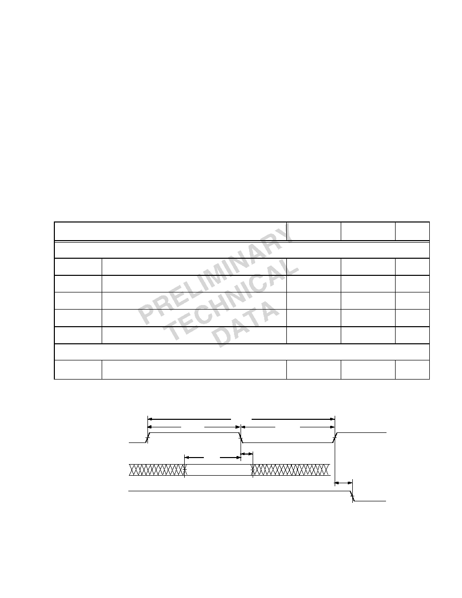
July 2000
ADSP-21161N Preliminary Data Sheet
For current information contact Analog Devices at (781) 461-3881
This information applies to a product under development. Its characteristics and specifications are subject to change with-
out notice. Analog Devices assumes no obligation regarding future manufacturing unless otherwise agreed to in writing.
54
REV. PrA
Link Ports
Calculation of link receiver data setup and hold relative to link clock is required to determine the
maximum allowable skew that can be introduced in the transmission path between LDATA and LCLK.
Setup skew is the maximum delay that can be introduced in LDATA relative to LCLK, (setup skew =
t
LCLKTWH
min t
DLDCH
t
SLDCL
). Hold skew is the maximum delay that can be introduced in LCLK
relative to LDATA, (hold skew = t
LCLKTWL
min t
HLDCH
t
HLDCL
). Calculations made directly from speed
specifications will result in unrealistically small skew times because they include multiple tester
guardbands. The setup and hold skew times shown below are calculated to include only one tester
guardband.
ADSP-21161N Setup Skew = TBD ns max
ADSP-21161N Hold Skew = TBD ns max
Note that there is a two-cycle effect latency between the link port enable instruction and the DSP
enabling the link port.
Figure 25 Link Ports--Receive
Table 24 Link Ports Receive
Parameter
Min
Max
Units
Timing Requirements
t
SLDCL
Data Setup Before LCLK Low
2
ns
t
HLDCL
Data Hold After LCLK Low
2
ns
t
LCLKIW
LCLK Period
t
LCLK
ns
t
LCLKRWL
LCLK Width Low
3.5
ns
t
LCLKRWH
LCLK Width High
3.5
ns
Switching Characteristics
t
DLALC
LACK Low Delay After LCLK High
1
1. LACK goes low with t
DLALC
relative to rise of LCLK after first nibble, but doesn't go low if the receiver's link buffer is not about to fill.
TBD
TBD
ns
LC LK
LDA T(7:0)
LA C K (O UT)
REC EIV E
IN
t
SLDC L
t
HLDC L
t
LC LKRW H
t
DLA LC
t
LC LKRW L
t
LC LKIW
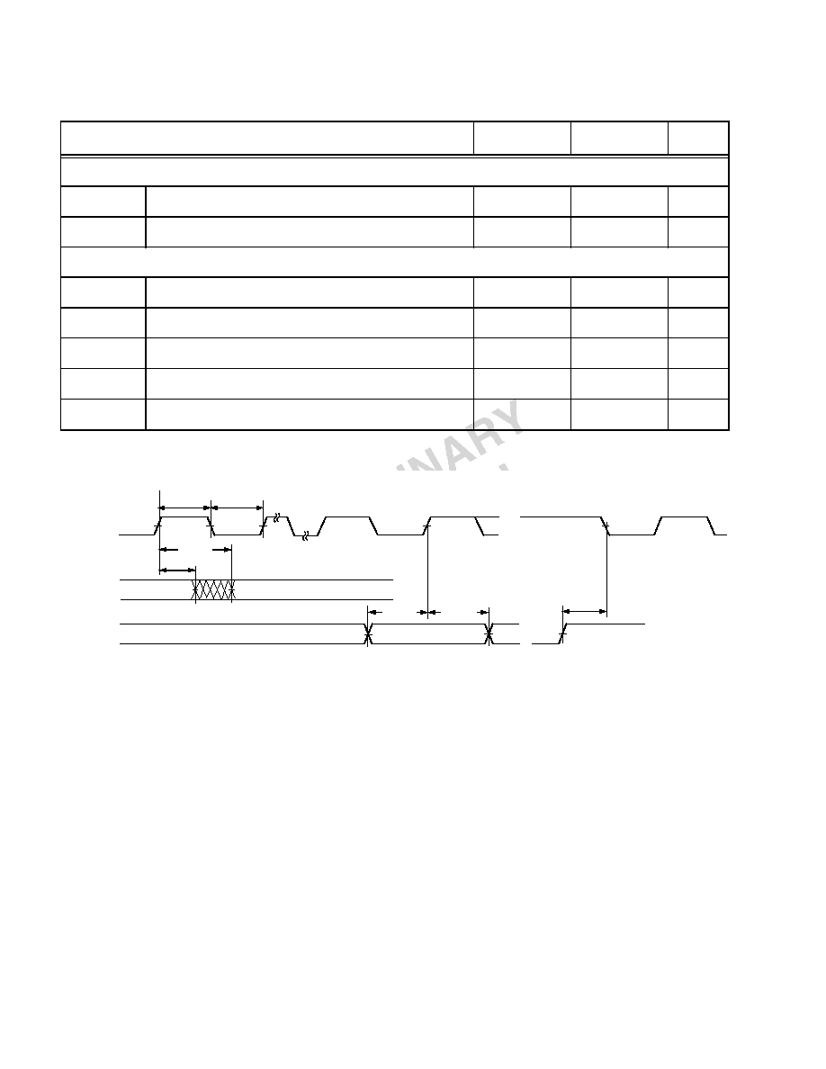
This information applies to a product under development. Its characteristics and specifications are subject to change with-
out notice. Analog Devices assumes no obligation regarding future manufacturing unless otherwise agreed to in writing.
ADSP-21161N Preliminary Data Sheet
July 2000
For current information contact Analog Devices at (781) 461-3881
55
REV. PrA
Figure 26 Link Ports--Transmit
Table 25 Link Ports Transmit
Parameter
Min
Max
Units
Timing Requirements
t
SLACH
LACK Setup Before LCLK High
15
ns
t
HLACH
LACK Hold After LCLK High
2
ns
Switching Characteristics
t
DLDCH
Data Delay After LCLK High
2
ns
t
HLDCH
Data Hold After LCLK High
2
ns
t
LCLKTWL
LCLK Width Low
.5t
LCLK
1
.5t
LCLK
+1
ns
t
LCLKTWH
LCLK Width High
.5t
LCLK
1
.5t
LCLK
+1
ns
t
DLACLK
LCLK Low Delay After LACK High
.5t
LCLK
+5
3t
LCLK
+11
ns
LC LK
LDA T(7:0)
LAC K (IN )
TH E
t
SLAC H REQ UIREM ENT A PPLIES TO TH E RISIN G EDG E O F LC LK O N LY FO R THE FIRST N IBBLE TRA NSM ITTED.
TRA N SM IT
LAST NIBBLE/BY TE
TRA NSM ITTED
FIRST NIBBLE/BY TE
TRA NSM ITTED
LC LK IN A C TIVE
(HIG H)
O UT
t
DLDC H
t
HLDC H
t
LC LKTW H
t
LC LKTW L
t
SLAC H
t
HLA C H
t
DLA C LK
July 2000
ADSP-21161N Preliminary Data Sheet
For current information contact Analog Devices at (781) 461-3881
This information applies to a product under development. Its characteristics and specifications are subject to change with-
out notice. Analog Devices assumes no obligation regarding future manufacturing unless otherwise agreed to in writing.
56
REV. PrA
Serial Ports
To determine whether communication is possible between two devices at clock speed n, the following
specifications must be confirmed: 1) frame sync delay & frame sync setup and hold, 2) data delay &
data setup and hold, and 3) SCLK width.
Table 26 Serial Ports--External Clock
Parameter
Min
Max
Units
Timing Requirements
t
SFSE
Transmit/Receive FS Setup Before Trans-
mit/Receive SCLK
1
1. Referenced to sample edge.
3.5
ns
t
HFSE
Transmit/Receive FS Hold After Trans-
mit/Receive SCLK
1, 2
2. FSx hold after Receive SCLK when MCE = 1, MFD = 0 is 0 ns minimum from drive edge. Transmit FS hold after Transmit SCLK for
late external Transmit FS is 0 ns minimum from drive edge.
4
ns
t
SDRE
Receive Data Setup Before Receive SCLK
1, 3
3. SCLK/FS Configured as a receive clock/frame sync with the DDIR bit = 0 in SPCTLx register.
1.5
ns
t
HDRE
Receive Data Hold After SCLK
1, 4
4. SCLK/FS Configured as a transmit clock/frame sync with the DDIR bit = 1 in SPCTLx register.
4
ns
t
SCLKW
SCLKx Width
9
ns
t
SCLK
SCLKx Period
2t
CCLK
ns
Table 27 Serial Ports--Internal Clock
Parameter
Min
Max
Units
Timing Requirements
t
SFSI
FS Setup Time Before SCLK
1
,
2
1. Referenced to sample edge.
2. SCLK/FS configured as a receive clock/frame sync with the DDIR bit = 0 in SPCTLx register.
8
ns
t
HFSI
FS Hold After SCLK
1, 2, 3
3. FSx hold after Receive SCLK when MCE = 1, MFD = 0 is 0 ns minimum from drive edge. Transmit FS hold after Transmit SCLK for
late external Transmit FS is 0 ns minimum from drive edge.
1
ns
t
SDRI
Receive Data Setup Before SCLK
1
3
ns
t
HDRI
Receive Data Hold After SCLK
1
3
ns
This information applies to a product under development. Its characteristics and specifications are subject to change with-
out notice. Analog Devices assumes no obligation regarding future manufacturing unless otherwise agreed to in writing.
ADSP-21161N Preliminary Data Sheet
July 2000
For current information contact Analog Devices at (781) 461-3881
57
REV. PrA
Table 28 Serial Ports--External or Internal Clock
Parameter
Min
Max
Units
Switching Characteristics
t
DFSE
FS Delay After SCLK (
1
)
(Internally Generated FS)
2
1. SCLK/FS Configured as a receive clock/frame sync with the DDIR bit = 0 in SPCTLx register.
2. Referenced to drive edge.
13
ns
t
HOFSE
FS Hold After Receive SCLK (
1
) (Internally Gen-
erated FS)
1
3
ns
Table 29 Serial Ports--External Clock
Parameter
Min
Max
Units
Switching Characteristics
t
DFSE
FS Delay After Transmit SCLK (Internally Gen-
erated Transmit FS)
1
,
2
1. Referenced to drive edge.
2. SCLK/FS Configured as a transmit clock/frame sync with the DDIR bit = 1 in SPCTLx register.
13
ns
t
HOFSE
FS Hold After Transmit SCLK (Internally Gener-
ated Transmit FS
1, 2
3
ns
t
DDTE
Transmit Data Delay After Transmit SLCK
1, 2
16
ns
t
HODTE
Transmit Data Hold After Transmit SCLK
1, 2
0
ns
Table 30 Serial Ports--Internal Clock
Parameter
Min
Max
Units
Switching Characteristics
t
DFSI
Transmit FS Delay After SCLK (Internally Gen-
erated Transmit FS)
1
,
2
4.5
ns
t
HOFSI
Transmit FS Hold After SCLK (Internally Gener-
ated Transmit FS)
1, 2
-1.5
ns
July 2000
ADSP-21161N Preliminary Data Sheet
For current information contact Analog Devices at (781) 461-3881
This information applies to a product under development. Its characteristics and specifications are subject to change with-
out notice. Analog Devices assumes no obligation regarding future manufacturing unless otherwise agreed to in writing.
58
REV. PrA
t
DDTI
Transmit Data Delay After SCLK
1, 2
7.5
ns
t
HDTI
Transmit Data Hold After SCLK
1, 2
0
ns
t
SCLKIW
Transmit or Receive SCLK Width
2
.5t
SCLK
2.5
.5t
SCLK
+2
ns
1. Referenced to drive edge.
2. SCLK/FS Configured as a transmit clock/frame sync with the DDIR bit = 1 in SPCTLx register.
Table 31 Serial Ports--Enable and Three-State
Parameter
Min
Max
Units
Switching Characteristics
t
DDTEN
Data Enable from External Transmit SCLK
1
,
2
1. Referenced to drive edge.
2. SCLK/FS Configured as a transmit clock/frame sync with the DDIR bit = 1 in SPCTLx register.
4
ns
t
DDTTE
Data Disable from External Transmit SCLK
1
10
ns
t
DDTIN
Data Enable from Internal Transmit SCLK
1
0
ns
t
DDTTI
Data Disable from Internal Transmit SCLK
1
3
ns
Table 32 Serial Ports--External Late Frame Sync
Parameter
Min
Max
Units
Switching Characteristics
t
DDTLFSE
Data Delay from Late External Transmit FS or
External Receive FS with MCE = 1, MFD = 0
1
1. MCE = 1, Transmit FS enable and Transmit FS valid follow t
DDTLFSE
and t
DDTENFS
.
13
ns
t
DDTENFS
Data Enable from Late FS or MCE = 1, MFD =
0
1
3.5
ns
Table 30 Serial Ports--Internal Clock
Parameter
Min
Max
Units
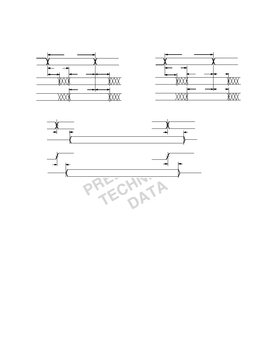
This information applies to a product under development. Its characteristics and specifications are subject to change with-
out notice. Analog Devices assumes no obligation regarding future manufacturing unless otherwise agreed to in writing.
ADSP-21161N Preliminary Data Sheet
July 2000
For current information contact Analog Devices at (781) 461-3881
59
REV. PrA
Figure 27 Serial Ports
DRIVE EDG E
DRIVE EDG E
DRIVE
EDG E
DRIVE
EDG E
SC LK
SC LK (IN T)
SC LK
SC LK (EXT)
t
DD TTE
t
DDTEN
t
DD TTI
t
DDTIN
SC LK
FS
DRIVE
EDG E
SAM PLE
EDG E
D A TA REC EIV E-- IN TERN A L C LO C K
D A TA REC EIV E-- EX TERN A L C LO C K
SC LK
FS
DRIVE
EDG E
SAM PLE
EDG E
N O TE: EITHER THE RISING EDG E OR FA LLING EDG E O F SC LK (EXTERN AL), SC LK (IN TERN A L) C A N BE USED AS THE AC TIVE SAM PLING EDG E.
t
SDRI
t
HDRI
t
SFSI
t
HFSI
t
DFSE
t
HO FSE
t
SC LKIW
t
SDRE
t
HDRE
t
SFSE
t
HFSE
t
DFSE
t
SC LKW
t
HO FSE
DxA /DxB
DxA /DxB
DxA /DxB
DxA /DxB
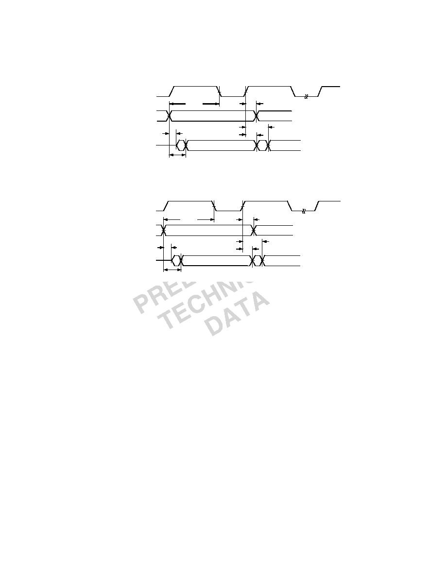
July 2000
ADSP-21161N Preliminary Data Sheet
For current information contact Analog Devices at (781) 461-3881
This information applies to a product under development. Its characteristics and specifications are subject to change with-
out notice. Analog Devices assumes no obligation regarding future manufacturing unless otherwise agreed to in writing.
60
REV. PrA
Figure 28 External Late Frame Sync
(SEE NO TE 2)
DRIVE SAM PLE
DRIVE
SC LK
FS
DxA/DxB
DRIVE SAM PLE
DRIVE
LA TE EX TERN A L TRA N SM IT FS
EX TERN A L REC EIV E FS W ITH M C E = 1, M FD = 0
1ST BIT
2N D BIT
SC LK
FS
1ST BIT
2N D BIT
(SEE NO TE 2)
t
HO FSE/I
t
SFSE/I
t
DDTE/I
t
DDTEN FS
t
DDTLFSE
t
HDTE/I
t
HO FSE/I
t
SFSE/I
t
DDTE/I
t
DDTEN FS
t
DDTLF SE
t
HDTE/I
DxA/DxB
This information applies to a product under development. Its characteristics and specifications are subject to change with-
out notice. Analog Devices assumes no obligation regarding future manufacturing unless otherwise agreed to in writing.
ADSP-21161N Preliminary Data Sheet
July 2000
For current information contact Analog Devices at (781) 461-3881
61
REV. PrA
SPI INTERFACE SPECIFICATIONS
Table 33 SPI Interface Protocol -- Timing Specifications
Name
Parameter
Mode
Min
Max
Units
t
SPICLK
Minimum serial clock cycle
Master
TBD
ns
t
SPICHM
Serial clock high period
Master
TBD
ns
t
SPICHS
Serial clock low period
Slave
TBD
ns
t
SPICLM
Serial clock low period
Master
TBD
ns
t
SPICLS
Serial clock high period
Slave
TBD
ns
t
SDSCO
SPIDS assertion to first SPICLK edge
CPHASE=0
CPHASE=1
t
SDSCI
CP0=1
Slave
Slave
TBD
TBD
ns
t
HDS
Last SPICLK edge to SPIDS not asserted
Slave
TBD
ns
t
SSPID
Data input valid to
SPICLK edge (data input set-up time)
Master/
Slave
TBD
ns
t
HSPID
SPICLK last sampling edge to data input not
valid
Master/
Slave
TBD
ns
t
DSOE
(
t
SPIDSOE)
SPIDS
assertion to data out active
Slave
TBD
ns
t
DSDHI
SPIDS
deassertion to data high impedance
Slave
TBD
ns
t
DDSPID
SPICLK edge to data out valid (data out delay
time)
Master/
Slave
TBD
ns
t
HDSPID
SPICLK edge to data out not valid (data out
hold time)
Master/
Slave
TBD
ns
t
DSOV
SPIDS
assertion to data out valid (CPHASE=0)
Slave
TBD
ns
t
SDPPW
SPIDS deassertion pulse width (CPHASE=0)
Slave
TBD
ns
July 2000
ADSP-21161N Preliminary Data Sheet
For current information contact Analog Devices at (781) 461-3881
This information applies to a product under development. Its characteristics and specifications are subject to change with-
out notice. Analog Devices assumes no obligation regarding future manufacturing unless otherwise agreed to in writing.
62
REV. PrA
Figure 29 SPI Master Timing (CPHA=0)
Figure 30 SPI Slave Timing (CPHA=0)
tSPICLK
tSPICLK
SPIDS
(Input)
MISO
(Input)
Va lid
MOSI
MS B
V a lid
LS B
MS
B
L S B
tSPICHS
tSPICLK
SPICLK (CPOL = 1
(Output)
tSPICHS
tSPICLS
tSPICLS
tSPICLK
tHSPID
tSSPID
tSSPID
tHSPID
tHDSPID
tDDSPID
SPICLK (CPOL = 0
(Output)
This information applies to a product under development. Its characteristics and specifications are subject to change with-
out notice. Analog Devices assumes no obligation regarding future manufacturing unless otherwise agreed to in writing.
ADSP-21161N Preliminary Data Sheet
July 2000
For current information contact Analog Devices at (781) 461-3881
63
REV. PrA
Figure 31 SPI Master Timing (CPHA=1)
SPIDS
(Input)
MISO
(Input)
Valid
MSB
Valid
LSB
MS B
L S B
SPICLK (CPOL = 0
(Output)
SPICLK (CPOL = 1
(Output)
tHSPID
tSPICHM
tSPICLM
tSPICLM
tSPICHM
tSPICLK
tHDSPID
tSSPID
tHSPID
tDDSPID
tSSPID
MOSI
(Output)
tSPICLK
July 2000
ADSP-21161N Preliminary Data Sheet
For current information contact Analog Devices at (781) 461-3881
This information applies to a product under development. Its characteristics and specifications are subject to change with-
out notice. Analog Devices assumes no obligation regarding future manufacturing unless otherwise agreed to in writing.
64
REV. PrA
Figure 32 SPI Slave Timing (CPHA=0)
MSB
Valid
SPIDS
(Input)
MISO
(Ouput)
tSPICLK
tSPICLS
tSPICHS
SPICLK (CPOL = 0)
tSPICLS
tSPICHS
tDSOE
tDDSPID
tHSPID
tHSPID
tSSPID
tSSPI
D
tHSPID
tSPIDSOE
tSDSCI
tDSOV
tHDS
tSDPPW
tSPICLK
(Input)
SPICLK (CPOL = 1)
(Input)
(Input)
MOSI
MSB
Valid
LSB
Valid
LSB
Valid
This information applies to a product under development. Its characteristics and specifications are subject to change with-
out notice. Analog Devices assumes no obligation regarding future manufacturing unless otherwise agreed to in writing.
ADSP-21161N Preliminary Data Sheet
July 2000
For current information contact Analog Devices at (781) 461-3881
65
REV. PrA
Figure 33 SPI Slave Timing (CPHA=1)
SPIDS
(Input)
MISO
(Output)
MOSI
(Input)
MSB
LSB
MSB
LSB
Valid
Valid
SCLK (CPOL = 0)
(Input)
SCLK (CPOL = 1)
(Input)
tSPICLS
tSPICHS
tSPICLK
tSDSCI
tHDS
tSSPID
tSSPID
tHSPID
tHSPID
tDSOE
tDSDHI
tDDSPID
tSPICHS
tSPICLS
tDSDHI
tSPIDSOE
This information applies to a product under development. Its characteristics and specifications are subject to change with-
out notice. Analog Devices assumes no obligation regarding future manufacturing unless otherwise agreed to in writing.
ADSP-21161N Preliminary Data Sheet
July 2000
For current information contact Analog Devices at (781) 461-3881
66
REV. PrA
Figure 34 IEEE 11499.1 JTAG Test Access Port
Table 34 JTAG Test Access Port and Emulation
Parameter
Min
Max Units
Timing Requirements
t
TCK
TCK Period
t
CK
ns
t
STAP
TDI, TMS Setup Before TCK High
5
ns
t
HTAP
TDI, TMS Hold After TCK High
6
ns
t
SSYS
System Inputs Setup Before TCK Low
1
7
ns
t
HSYS
System Inputs Hold After TCK Low
1
18
ns
t
TRSTW
TRST Pulse Width
4t
CK
ns
Switching Characteristics
t
DTDO
TDO Delay from TCK Low
13
ns
t
DSYS
System Outputs Delay After TCK Low
2
18
ns
1. System Inputs = DATA
47-16
, ADDR
23-0
, RD, WR, ACK, RPBA, SPIDS, EBOOT, LBOOT, DMAR
2-1,
CLK_CFG
1-0
, CLKDBL,
CS, HBR, SBTS, ID
2-0
, IRQ
2-0
, RESET, BMS, MISO, MOSI, SPICLK, DxA, DxB, SCLKx, FSx, LxDAT
7-0
, LxCLK,
LxACK, SDWE, HBG, RAS, CAS, SDCLK0, SDCKE, BRST, BR
6-1
, PA, MS
3-0
, FLAG
11-0
2. System Outputs = BMS, MISO, MOSI, SPICLK, DxA, DxB, SCLKx, FSx, LxDAT
7-0
, LxCLK, LxACK, DATA
47-16
, SDWE, ACK,
HBG, RAS, CAS, SDCLK
1-0
, SDCKE, BRST, RD, WR, BR
6-1
, PA, MS
3-0
, ADDR
23-0
, FLAG
11-0
, DMAG
2-1
, DQM, REDY,
CLKOUT, SDA10, TIMEXP, EMU, BMSTR.
TC K
TM S
TDI
TDO
SYSTEM
IN PUTS
SYSTEM
OUTPUTS
t
STA P
t
TC K
t
HTAP
t
DTDO
t
SSYS
t
HSYS
t
DSYS
This information applies to a product under development. Its characteristics and specifications are subject to change with-
out notice. Analog Devices assumes no obligation regarding future manufacturing unless otherwise agreed to in writing.
ADSP-21161N Preliminary Data Sheet
July 2000
For current information contact Analog Devices at (781) 461-3881
67
REV. PrA
OUTPUT DRIVE CURRENTS
Figure 38 on page 70
shows typical I-V characteristics for the output drivers of the ADSP-21161N.
The curves represent the current drive capability of the output drivers as a function of output voltage.
POWER DISSIPATION
Total power dissipation has two components: one due to internal circuitry and one due to the switching
of external output drivers.
Internal power dissipation is dependent on the instruction execution sequence and the data operands
involved. Using the current specifications (I
DDINPEAK
, I
DDINHIGH
, I
DDINLOW
, I
DDIDLE
) from
Table
5 on page 25
and the current-versus-operation information in
Table 35
, you can estimate the
ADSP-21161N's internal power supply (V
DDINT
) input current for a specific application, according to
the following formula:
%Peak
×
I
DDINPEAK
%High
×
I
DDINHIGH
%Low
×
I
DDINLOW
+
%Idle
×
I
DDIDLE
I
DDINT
The external component of total power dissipation is caused by the switching of output pins. Its
magnitude depends on:
·
The number of output pins that switch during each cycle (O)
·
The maximum frequency at which they can switch (f)
Table 35 ADSP-21161N Operation Types Versus Input Current
Operation
Peak Activity
1
(I
DDINPEAK
)
1. The state of the PEYEN bit (SIMD versus SISD mode) does not influence these calculations.
High Activity
1
(I
DDINHIGH
)
Low Activity
1
(I
DDINLOW
)
Instruction Type
Multifunction
Multifunction
Single Function
Instruction Fetch
Cache
Internal Memory
Internal Memory
Core Memory Access
2
2. These assume a 2:1 core clock ratio. For more information on ratios and clocks (t
CK
and t
CCLK
), see the timing ratio definitions
on page 27
.
2 per t
CK
cycle
(DM
×64
and PM
×64
)
1 per t
CK
cycle
(DM
×64
)
None
Internal Memory DMA
1 per 2 t
CCLK
cycles
1 per 2 t
CCLK
cycles
N/A
External Memory DMA
1 per external port
cycle (
×32)
1 per external port
cycle (
×32)
N/A
Data bit pattern for core
memory access and DMA
Worst case
Random
N/A
This information applies to a product under development. Its characteristics and specifications are subject to change with-
out notice. Analog Devices assumes no obligation regarding future manufacturing unless otherwise agreed to in writing.
ADSP-21161N Preliminary Data Sheet
July 2000
For current information contact Analog Devices at (781) 461-3881
68
REV. PrA
·
Their load capacitance (C)
·
Their voltage swing (VDD)
and is calculated by:
PEXT = O × C × VDD
2
× f
The load capacitance should include the processors package capacitance (Cin). The switching frequency
includes driving the load high and then back low. Address and data pins can drive high and low at a
maximum rate of 1
tck
while writing to a SDDRAM Memory.
Example:
Estimate Pext with the following assumptions:
·
A system with one bank of external memory (32 bit)
·
Two 1M x 16 SDRAM chips are used, each with a load of 10pF
·
External Data Memory writes can occur every cycle at a rate of 1/tck, with 50% of the pins switch-
ing
·
The bus cycle time is 50Mhz
·
The external SDRAM clock rate is 100Mhz
The PEXT equation is calculated for each class of pins that can drive:
A typical power consumption can now be calculated for these conditions by adding a typical internal
power dissipation:
P
TOTAL
= P
EXT
+ P
INT
+ P
PLL
Where:
P
EXT
is from
Table 36
P
INT
is I
DDINT
× 1.8V, using the calculation I
DDINT
listed in
"Power Dissipation" on page 67
P
PLL
is AI
DD
× 1.8V, using the value for AI
DD
listed in
Table 5 on page 25
Note that the conditions causing a worst-case PEXT are different from those causing a worst-case
PINT. Maximum PINT cannot occur while 100% of the output pins are switching from all ones to all
Table 36 External Power Calculations (3.3 V Device)
Pin Type
# of Pins
%
Switching
× C
× f
× VDD
2
= P
EXT
Address
11
50
× 44.7 pF
50 MHz
× 10.9 V
= 0.134 W
MSx
4
0
× 44.7 pF
-
× 10.9 V
= 0.000 W
SDWE
1
1
× 44.7 pF
-
× 10.9 V
= 0.024 W
Data
32
50
× 14.7 pF
50 MHz
× 10.9 V
= 0.128 W
SDCLK0
1
-
× 10.7 pF
100 MHz
× 10.9 V
= 0.012 W
P
EXT
= 0.298 W
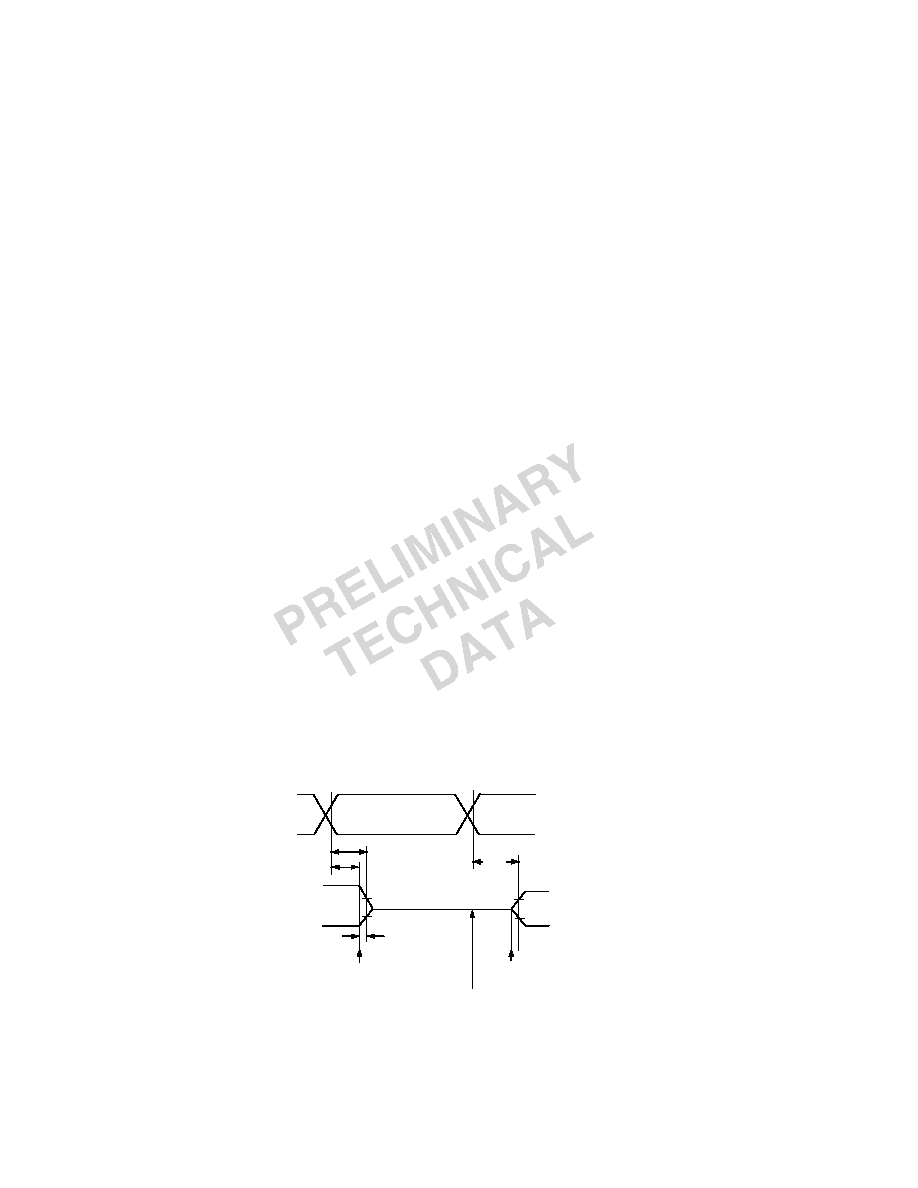
This information applies to a product under development. Its characteristics and specifications are subject to change with-
out notice. Analog Devices assumes no obligation regarding future manufacturing unless otherwise agreed to in writing.
ADSP-21161N Preliminary Data Sheet
July 2000
For current information contact Analog Devices at (781) 461-3881
69
REV. PrA
zeros. Note also that it is not common for an application to have 100% or even 50% of the outputs
switching simultaneously.
TEST CONDITIONS
Output Disable Time
Output pins are considered to be disabled when they stop driving, go into a high impedance state, and
start to decay from their output high or low voltage. The time for the voltage on the bus to decay by
V is dependent on the capacitive load, CL and the load current, IL. This decay time can be
approximated by the following equation:
t
DECAY
= (C
L
V)/I
L
The output disable time t
DIS
is the difference between t
MEASURED
and t
DECAY
as shown in Figure 25. The
time t
MEASURED
is the interval from when the reference signal switches to when the output voltage decays
V from the measured output high or output low voltage. t
DECAY
is calculated with test loads CL and
IL, and with V equal to 0.5 V.
Output Enable Time
Output pins are considered to be enabled when they have made a transition from a high impedance
state to the point when they start driving. The output enable time t
ENA
is the interval from the point
when a reference signal reaches a high or low voltage level to the point when the output has reached a
specified high or low trip point, as shown in the Output Enable/Disable diagram (
Figure 35
). If
multiple pins (such as the data bus) are enabled, the measurement value is that of the first pin to start
driving.
Example System Hold Time Calculation
To determine the data output hold time in a particular system, first calculate t
DECAY
using the equation
given above. Choose V to be the difference between the ADSP-21161N's output voltage and the input
threshold for the device requiring the hold time. A typical V will be 0.4 V. CL is the total bus
capacitance (per data line), and IL is the total leakage or three-state current (per data line). The hold
time will be t
DECAY
plus the minimum disable time (i.e., t
DATRWH
for the write cycle).
Figure 35 Output Enable/Disable
REFEREN C E
SIG NAL
tDIS
O UTPUT STARTS
DRIVING
VOH (MEASURED) - DV
VOL (MEASURED) + DV
tMEASURED
VOH (MEASURED)
VOL (MEASURED)
2.0V
1.0V
VOH (MEASURED)
VOL (MEASURED)
HIG H-IM PEDA NC E STATE.
TEST C O N DITIO N S C A USE THIS
VO LTAG E TO BE A PPRO XIM ATELY 1.5V
O UTPUT STO PS
DRIVING
tENA
tDECAY
This information applies to a product under development. Its characteristics and specifications are subject to change with-
out notice. Analog Devices assumes no obligation regarding future manufacturing unless otherwise agreed to in writing.
ADSP-21161N Preliminary Data Sheet
July 2000
For current information contact Analog Devices at (781) 461-3881
70
REV. PrA
Figure 36 Equivalent Device Loading for AC Measurements (Includes All Fixtures)
Figure 37 Voltage Reference Levels for AC Measurements (Except Output Enable/Disable)
Capacitive Loading
Output delays and holds are based on standard capacitive loads: 50 pF on all pins (see
Figure 36 on
page 70
). The delay and hold specifications given should be derated by a factor of 1.5 ns/50 pF for loads
other than the nominal value of 50 pF. Figures 31-32, 34-35 show how output rise time varies with
capacitance. Figures 33, 37 show graphically how output delays and holds vary with load capacitance
(Note that this graph or derating does not apply to output disable delays; see
"Output Disable Time"
on page 69
.). The graphs of Figures 31, 32 and 33 may not be linear outside the ranges shown.
Figure 38 ADSP-21161N Typical Drive Currents
+1.5V
50pF
TO
O UTP UT
PIN
IOL
IOH
INPUT
O R
O UTP UT
1.5V
1.5V
SOURCE (VDDEXT) VOLTAG E - V
120
-20
-80
0
3.5
0.5
1
1.5
2
2.5
3
100
0
-40
-60
60
20
80
40
-100
-120
S
O
U
R
C
E
(
VDDE
X
T
)
C
U
RRE
N
T
-
m
A
3.47V, 0°C
3.3V, +25°C
3.13V, +85°C
VOH
3.13V, +85°C
3.3V, +25°C
3.47V, 0°C
VOL
This information applies to a product under development. Its characteristics and specifications are subject to change with-
out notice. Analog Devices assumes no obligation regarding future manufacturing unless otherwise agreed to in writing.
ADSP-21161N Preliminary Data Sheet
July 2000
For current information contact Analog Devices at (781) 461-3881
71
REV. PrA
Figure 39 Typical Output Rise Time (10%-90%, V
DDEXT
=Max) vs. Load Capacitance
Figure 40 Typical Output Rise Time (10%-90%, V
DDEXT
=Min) vs. Load Capacitance
Figure 41 Typical Output Delay or Hold vs. Load Capacitance (at Max Case Temperature)
LO A D C A PA C ITA NC E - pF
16.0
8.0
0
0
200
20
40
60
80
100
120
140
160
180
14.0
12.0
4.0
2.0
10.0
6.0
FALL TIM E
RISE TIM E
Y = TBD
Y = TBD
R
I
S
E
A
N
D
F
A
LL T
I
M
E
S
-
n
s
(
0
.
35v
-
3.
12
v,
10%
-
90
%)
3.5
0
3.0
2.5
2.0
1.5
1.0
0.5
LO A D C APA C ITAN C E - pF
0
200
20
40
60
80
100
120
140
160
180
FALL TIM E
RISE TIM E
Y = TBD
Y =TBD
R
I
S
E
AND
F
A
L
L
T
I
M
E
S
-
n
s
(
0
.
3
1
-
2.
8
2
,
10
%
-
90%
)
LO A D C A PA C ITA NC E - pF
5
-
25
200
50
75
100
125
150
175
4
3
2
1
N O M INA L
Y = TBD
OU
T
P
U
T
D
E
L
A
Y
OR
H
O
LD
- n
s
This information applies to a product under development. Its characteristics and specifications are subject to change with-
out notice. Analog Devices assumes no obligation regarding future manufacturing unless otherwise agreed to in writing.
ADSP-21161N Preliminary Data Sheet
July 2000
For current information contact Analog Devices at (781) 461-3881
72
REV. PrA
ENVIRONMENTAL CONDITIONS
Thermal Characteristics
The ADSP-21161N is packaged in a 225-lead Plastic Ball Grid Array (PBGA). The ADSP-21161N is
specified for a case temperature (T
CASE
). To ensure that the T
CASE
data sheet specification is not
exceeded, a heatsink and/or an air flow source may be used. Use the center block of ground pins (PBGA
balls: F6-10, G6-10, H6-10, J6-10, K6-10) to provide thermal pathways to your printed circuit board's
ground plane. A heatsink should be attached to the ground plane (as close as possible to the thermal
pathways) with a thermal adhesive.
T
CASE
= T
AMB
+ (PD ×
CA
)
T
CASE
= Case temperature (measured on top surface of package)
PD =
Power dissipation in W (this value depends upon the specific application; a method for
calculating PD is shown under Power Dissipation).
CA
=
Value from table below.
JB
=
TBD
°
C/W
NOTES
·
This represents thermal resistance at total power of TBD W.
·
With air flow, no variance is seen in
CA
with power.
·
CA
at 0 LFM varies with power: At [DATA NOT AVAILABLE- TBD.].
·
JC
= TBD
°
C/W
Airflow (Linear Ft./Min.)
TBD
TBD
TBD
TBD
TBD
Airflow (Meters/Second)
TBD
TBD
TBD
TBD
TBD
CA
(
°
C/W)
1
1. These are preliminary estimates.
TBD
TBD
TBD
TBD
TBD
This information applies to a product under development. Its characteristics and specifications are subject to change with-
out notice. Analog Devices assumes no obligation regarding future manufacturing unless otherwise agreed to in writing.
ADSP-21161N Preliminary Data Sheet
July 2000
For current information contact Analog Devices at (781) 461-3881
73
REV. PrA
225-BALL METRIC PBGA PIN CONFIGURATIONS
Table 37 225-Lead Metric PBGA Pin Assignments
Pin Name
PBGA Pin#
Pin Name
PBGA Pin#
Pin Name
PBGA Pin#
Pin Name
PBGA Pin#
NC
A01
TRST_B
B01
TMS
C01
TDO
D01
BMSTR
A02
TDI
B02
EMU_B
C02
TCK
D02
BMS_B
A03
RPBA
B03
GND
C03
FLAG11
D03
SPIDS
A04
MOSI
B04
SPICLK
C04
MISO
D04
EBOOT
A05
SFS0
B05
SD0B
C05
SCLK0
D05
LBOOT
A06
SCLK1
B06
SD1A
C06
SD1B
D06
SCLK2
A07
SD2B
B07
SD2A
C07
SFS1
D07
SD3B
A08
SD3A
B08
SFS2
C08
VDDINT
D08
L0DAT[4]
A09
L0DAT[7]
B09
SFS3
C09
SCLK3
D09
L0ACK
A10
L0CLK
B10
L0DAT[6]
C10
L0DAT[5]
D10
L0DAT[2]
A11
L0DAT[1]
B11
L1DAT[7]
C11
L0DAT[3]
D11
L1DAT[6]
A12
L1DAT[4]
B12
L1DAT[3]
C12
L1DAT[5]
D12
L1CLK
A13
L1ACK
B13
L1DAT[1]
C13
DATA[42]
D13
L1DAT[2]
A14
L1DAT[0]
B14
DATA[45]
C14
DATA[46]
D14
NC
A15
NC
B15
DATA[47]
C15
DATA[44]
D15
FLAG10
E01
FLAG5
F01
FLAG1
G01
FLAG0
H01
RESET_B
E02
FLAG7
F02
FLAG2
G02
IRQ0_B
H02
FLAG8
E03
FLAG9
F03
FLAG4
G03
VDDINT
H03
SD0A
E04
FLAG6
F04
FLAG3
G04
IRQ1_B
H04
VDDEXT
E05
VDDINT
F05
VDDEXT
G05
VDDINT
H05
VDDINT
E06
GND
F06
GND
G06
GND
H06
VDDEXT
E07
GND
F07
GND
G07
GND
H07
VDDINT
E08
GND
F08
GND
G08
GND
H08
VDDEXT
E09
GND
F09
GND
G09
GND
H09
VDDINT
E10
GND
F10
GND
G10
GND
H10
VDDEXT
E11
VDDINT
F11
VDDEXT
G11
VDDINT
H11
L0DAT[0]
E12
DATA[37]
F12
DATA[34]
G12
DATA[29]
H12
DATA[39]
E13
DATA[40]
F13
DATA[35]
G13
DATA[28]
H13
DATA[43]
E14
DATA[38]
F14
DATA[33]
G14
DATA[30]
H14
This information applies to a product under development. Its characteristics and specifications are subject to change with-
out notice. Analog Devices assumes no obligation regarding future manufacturing unless otherwise agreed to in writing.
ADSP-21161N Preliminary Data Sheet
July 2000
For current information contact Analog Devices at (781) 461-3881
74
REV. PrA
DATA[41]
E15
DATA[36]
F15
DATA[32]
G15
DATA[31]
H15
IRQ2_B
J01
TIMEXP
K01
ADDR[19]
L01
ADDR[16]
M01
ID1
J02
ADDR[22]
K02
ADDR[17]
L02
ADDR[12]
M02
ID2
J03
ADDR[20]
K03
ADDR[21]
L03
ADDR[18]
M03
ID0
J04
ADDR[23]
K04
ADDR[2]
L04
ADDR[6]
M04
VDDEXT
J05
VDDINT
K05
VDDEXT
L05
ADDR[0]
M05
GND
J06
GND
K06
VDDINT
L06
MS1_B
M06
GND
J07
GND
K07
VDDEXT
L07
BR6_B
M07
GND
J08
GND
K08
VDDINT
L08
VDDEXT
M08
GND
J09
GND
K09
VDDEXT
L09
WRL_B
M09
GND
J10
GND
K10
VDDINT
L10
SDA10
M10
VDDEXT
J11
VDDINT
K11
VDDEXT
L11
RAS_B
M11
DATA[26]
J12
DATA[22]
K12
CAS_B
L12
ACK
M12
DATA[24]
J13
DATA[19]
K13
DATA[20]
L13
DATA[17]
M13
DATA[25]
J14
DATA[21]
K14
DATA[16]
L14
DMAG2_B
M14
DATA[27]
J15
DATA[23]
K15
DATA[18]
L15
DMAG1_B
M15
ADDR[14]
N01
ADDR[13]
P01
NC
R01
ADDR[15]
N02
ADDR[9]
P02
ADDR[11]
R02
ADDR[10]
N03
ADDR[8]
P03
ADDR[7]
R03
ADDR[5]
N04
ADDR[4]
P04
ADDR[3]
R04
ADDR[1]
N05
MS2_B
P05
MS3_B
R05
MS0_B
N06
SBTS_B
P06
PA_B
R06
BR5_B
N07
BR4_B
P07
BR3_B
R07
BR2_B
N08
BR1_B
P08
RDL_B
R08
BRST
N09
SDCLK1
P09
CLKOUT
R09
SDCKE
N10
SDCLK0
P10
HBR_B
R10
CS_B
N11
REDY
P11
HBG_B
R11
CLK_CFG1
N12
CLKIN
P12
CLKDBL
R12
CLK_CFG0
N13
DQM
P13
XTAL
R13
AVDD
N14
AVSS
P14
SDWE_B
R14
DMAR1_B
N15
DMAR2_B
P15
NC
R15
Table 37 225-Lead Metric PBGA Pin Assignments (Continued)
Pin Name
PBGA Pin#
Pin Name
PBGA Pin#
Pin Name
PBGA Pin#
Pin Name
PBGA Pin#
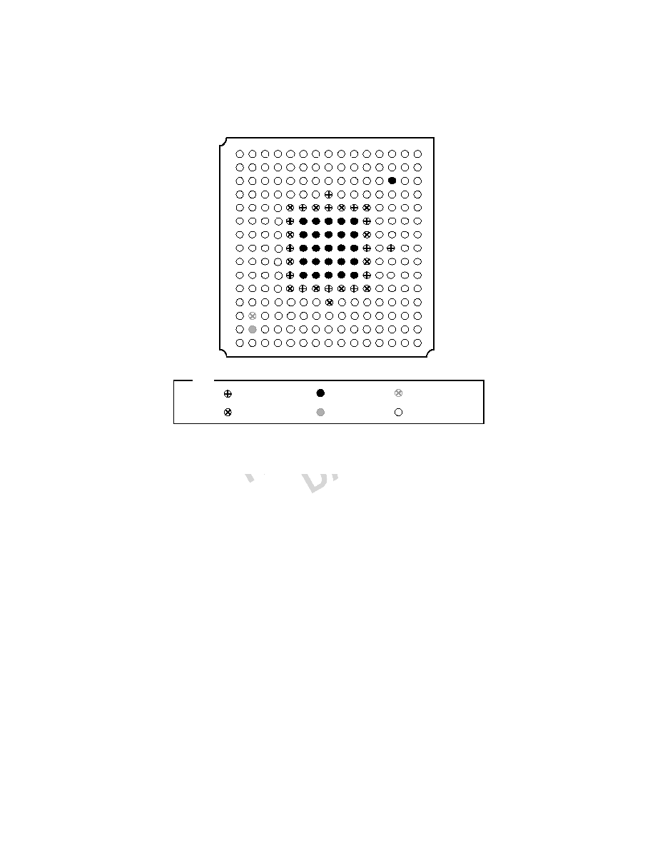
This information applies to a product under development. Its characteristics and specifications are subject to change with-
out notice. Analog Devices assumes no obligation regarding future manufacturing unless otherwise agreed to in writing.
ADSP-21161N Preliminary Data Sheet
July 2000
For current information contact Analog Devices at (781) 461-3881
75
REV. PrA
Figure 42 225-Lead Metric PBGA Pin Assignments (Bottom View, Summary)
V D D INT
V D D EX T
G N D *
A V SS
A V DD
SIG N A L
KEY :
* U se the c en ter b lo c k o f grou nd p ins
to p ro vid e th erm a l p a th w a ys to you r
p rinte d c irc uit b oa rd 's g rou nd p la ne .
1
2
3
4
5
6
7
8
9
10
11
12
14
15
13
R
P
N
M
L
K
J
H
G
F
E
D
C
B
A
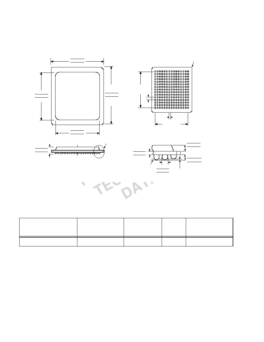
This information applies to a product under development. Its characteristics and specifications are subject to change with-
out notice. Analog Devices assumes no obligation regarding future manufacturing unless otherwise agreed to in writing.
ADSP-21161N Preliminary Data Sheet
July 2000
For current information contact Analog Devices at (781) 461-3881
76
REV. PrA
PACKAGE DIMENSIONS
The ADSP-21161N comes in a 17mm × 17mm, 225 ball PBGA package with 15 rows of balls. All
dimensions in
Figure 43
are in millimeters (mm).
Figure 43 Package Dimensions Metric 17mm × 17mm, 225 ball PBGA
ORDERING GUIDE
Part Number
1
1. These parts are packaged in a 225-lead Plastic Ball Grid Array (PBGA).
Case Temperature
Range
2
2. Parts for the industrial temperature ranges will be available in 2000.
Instruction
Rate
On-Chip
SRAM
Operating Voltage
ADSP-21161N-KB-100X
0
°
C to +85
°
C
100 MHz
1 Mbit
1.8 INT/3.3 EXT V
1.00
BSC
14.00
BSC
1
2
3
4
5
6
7
8
9
10
11
12
14
15
13
R
P
N
M
L
K
J
H
G
F
E
D
C
B
A
1.00 BSC
14.00 BSC
17.20
17.00
16.80
17.20
17.00
16.80
14.80
15.00
15.20
14.80
15.00
15.20
TOP VIEW
1.90
1.60
1.30
DETAIL A
NOTE
THE ACTUAL POSITION OF THE BALL GRID IS WITHIN 0.30mm OF ITS IDEAL
POSITION RELATIVE TO THE PACKAGE EDGES.
THE ACTUAL POSITION OF EACH BALL IS WITHIN 0.10mm OF ITS IDEAL
POSITION RELATIVE TO THE BALL GRID.
SEATING
PLANE
.65 (min)
.75 (typical)
.85 (max)
0.20 MAX
DETAIL A
0.70
0.60
0.50
BALL DIAMETER
0.45
0.35
0.25
0.40 (min)
0.50 (typical)
0.60 (max)
(BOTTOM VIEW)
A1 BALL PAD
CORNER
Document Outline