Äîêóìåíòàöèÿ è îïèñàíèÿ www.docs.chipfind.ru
a
Preliminary Technical Data
SHARC and the SHARC logo are registered trademarks of Analog Devices, Inc.
SHARC
®
Processor
ADSP-21364
Rev. PrB
Information furnished by Analog Devices is believed to be accurate and reliable.
However, no responsibility is assumed by Analog Devices for its use, nor for any
infringements of patents or other rights of third parties that may result from its use.
Specifications subject to change without notice. No license is granted by implication
or otherwise under any patent or patent rights of Analog Devices. Trademarks and
registered trademarks are the property of their respective companies.
One Technology Way, P.O. Box 9106, Norwood, MA 02062-9106 U.S.A.
Tel:781.329.4700
www.analog.com
Fax:781.326.8703
© 2004 Analog Devices, Inc. All rights reserved.
SUMMARY
High performance 32-bit/40-bit floating point processor
optimized for professional audio processing
At 333 MHz/2 GFLOPs, with unique audio centric peripherals
such as the Digital Audio Interface that includes a high-
precision 8-channel asynchronous sample rate converter
among others, the ADSP-21364 SHARC processor is ideal
for applications that require industry leading equalization,
reverberation and other effects processing
Single-Instruction Multiple-Data (SIMD) computational
architecture
Two 32-bit IEEE floating-point/32-bit fixed-point/40-bit
extended precision floating-point computational units,
each with a multiplier, ALU, shifter, and register file
On-chip memory--3M bit of on-chip SRAM and a dedicated
4M bit of on-chip mask-programmable ROM
Code compatible with all other members of the SHARC family
The ADSP-21364 is available with a 333 MHz core instruction
rate and unique audio centric peripherals such as the Digi-
tal Audio Interface, S/PDIF transceiver, serial ports, 8-
channel asynchronous sample rate converter, precision
clock generators and more. For complete ordering infor-
mation, see
Ordering Guide on Page 52
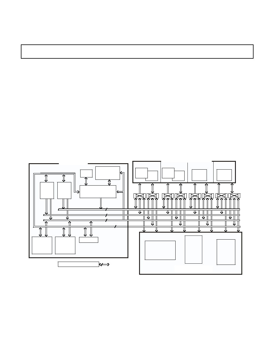
Figure 1. Functional Block Diagram Processor Core
ADDR
DATA
IOD
ADDR
DATA
IOA
ADDR
DATA
IOA
SRAM
1M BIT
ROM
2M BIT
SRAM
0.5M BIT
BLOCK 0
BLOCK 1
BLOCK 2
BLOCK 3
ADDR
DATA
IOA
IOP REGISTERS
(MEMORY MAPPED)
SEE "ADSP-21364 MEMORY
AND I/O INTERFACE FEATURES"
SECTION FOR DETAILS
I/O PROCESSOR
AND PERIPHERALS
6
JTAG TEST & EMULATION
32
PM ADDRESS BUS
DM ADDRESS BUS
32
PM DATA BUS
DM DATA BUS
64
64
PX REGISTER
PROCESSING
ELEMENT
(PEY)
PROCESSING
ELEMENT
(PEX)
TIMER
INSTRUCTION
CACHE
32 X 48-BIT
DAG1
8X4X32
DAG2
8X4X32
CORE PROCESSOR
PROGRAM
SEQUENCER
SRAM
1M BIT
ROM
2M BIT
SIGNAL
ROUTING
UNIT
SRAM
0.5M BIT
4 BLOCKS OF ON-CHIP MEMORY
IOD
IOA
IOD
IOD
SPI
SPORTS
IDP
PCG
TIMERS
SRC
SPDIF
S

DR
AF
T
Rev. PrB
|
Page 2 of 52
|
September 2004
ADSP-21364
Preliminary Technical Data
KEY FEATURES PROCESSOR CORE
At 333 MHz (3.0 ns) core instruction rate, the ADSP-21364
performs 2 GFLOPS/666 MMACS
3M bit on-chip single-ported SRAM (1M Bit in blocks 0 and 1,
and 0.50M Bit in blocks 2 and 3) for simultaneous access by
core processor and DMA
4M bit on-chip single-ported mask-programmable ROM (2M
bit in block 0 and 2M bit in block 1)
Dual Data Address Generators (DAGs) with modulo and
bit-reverse addressing
Zero-overhead looping with single-cycle loop setup, provid-
ing efficient program sequencing
Single Instruction Multiple Data (SIMD) architecture
provides:
Two computational processing elements
Concurrent execution
Code compatibility with other SHARC family members at
the assembly level
Parallelism in busses and computational units allows sin-
gle cycle execution (with or without SIMD) of a multiply
or ALU operation, a dual memory read or write, and an
instruction fetch
Transfers between memory and core at a sustained 5.4
Gbytes/s bandwidth at 333 MHz core instruction rate
INPUT/OUTPUT FEATURES
DMA Controller supports:
25 DMA channels for transfers between ADSP-21364 internal
memory a variety of peripherals
32-bit DMA transfers at core clock speed, in parallel with full-
speed processor execution
Asynchronous parallel port provides access to asynchronous
external memory
16 multiplexed address/data lines support 24-bit address
external address range with 8-bit data or 16-bit address
external address range with 16-bit data
55 Mbyte per sec transfer rate
External memory access in a dedicated DMA channel
8- to 32- bit and 16- to 32-bit packing options
Programmable data cycle duration: 2 to 31 CCLK
Digital audio interface (DAI) includes six serial ports, two Pre-
cision Clock Generators, an Input Data Port, three timers,
eight-channel asynchronous sample rate converter, and a
Signal routing unit
Six dual data line serial ports that operate at up to 50M bit/s
on each data line--each has a clock, frame sync and two
data lines that can be configured as either a receiver or
transmitter pair
Left-justified Sample Pair and I
2
S Support, programmable
direction for up to 24 simultaneous receive or transmit
channels using two I
2
S compatible stereo devices per serial
port
TDM support for telecommunications interfaces including
128 TDM channel support for newer telephony interfaces
such as H.100/H.110
Up to 12 TDM stream support, each with 128 channels per
frame
Companding selection on a per channel basis in TDM mode
Input data port provides an additional input path to the
SHARC core, configurable as eight channels of serial data
or seven channels of serial data and a single channel of up
to 20-bit wide parallel data
Signal routing unit provides configurable and flexible con-
nections between all DAI componentssix serial ports, two
precision clock generators, an input data port with a data
acquisition port, one SPI port, eight channels of asynchro-
nous sample rate converters, three timers, 10 interrupts,
six flag inputs, six flag outputs, and 20 SRU I/O pins
(DAI_Px)
Two Serial Peripheral Interfaces (SPI): primary on dedicated
pins, secondary on DAI pins provide:
Master or slave serial boot through primary SPI
Full-duplex operation
Master-Slave mode multi-master support
Open drain outputs
Programmable baud rates, clock polarities and phases
3 Muxed Flag/IRQ lines
1 Muxed Flag/Timer expired line
DEDICATED AUDIO COMPONENTS
S/PDIF Compatible Digital Audio receiver/transmitter
supports:
EIAJ CP-340 (CP-1201), IEC-958, AES/EBU standards
Left justified, I
2
S or right justified serial data input with 16,
18, 20 or 24 bit word widths (transmitter)
Two channel mode and Single Channel Double Frequency
(SCDF) mode
Sample Rate Converter (SRC) Contains a Serial Input Port, De-
emphasis Filter providing up to -140db SNR performance,
Sample Rate Converter (SRC) and Serial Output Port
Supports Left Justified, I
2
S, TDM and Right Justified 24, 20,
18 and 16 bit serial formats (input)
Pulse Width Modulation provides:
16 PWM outputs configured as four groups of four outputs
Supports center-aligned or edge-aligned PWM waveforms
Can generate complementary signals on two outputs in
paired mode or independent signals in nonpaired mode
PLL has a wide variety of software and hardware multi-
plier/divider ratios
Dual voltage: 3.3 V I/O, 1.2 V core
Available in 136-ball Mini-BGA and 144-lead LQFP Packages

ADSP-21364
Preliminary Technical Data
Rev. PrB
|
Page 3 of 52
|
September 2004
GENERAL DESCRIPTION
The ADSP-21364 SHARC processor is a member of the SIMD
SHARC family of DSPs that feature Analog Devices' Super Har-
vard Architecture. The ADSP-21364 is source code compatible
with the ADSP-2126x, and ADSP-2116x DSPs as well as with
first generation ADSP-2106x SHARC processors in SISD (Sin-
gle-Instruction, Single-Data) mode. The ADSP-21364 is a 32-
bit/40-bit floating point processor optimized for professional
audio applications with a large on-chip SRAM, multiple internal
buses to eliminate I/O bottlenecks, and an innovative Digital
Audio Interface (DAI).
As shown in the functional block diagram
on Page 1
, the
ADSP-21364 uses two computational units to deliver a signifi-
cant performance increase over previous SHARC processors on
a range of signal processing algorithms. Fabricated in a state-of-
the-art, high speed, CMOS process, the ADSP-21364 processor
achieves an instruction cycle time of 3.0 ns at 333 MHz. With its
SIMD computational hardware, the ADSP-21364 can perform 2
GFLOPS running at 333 MHz.
Table 1
shows performance benchmarks for the ADSP-21364.
The ADSP-21364 continues SHARC's industry leading stan-
dards of integration for DSPs, combining a high performance
32-bit DSP core with integrated, on-chip system features.
The block diagram of the ADSP-21364
on Page 1
, illustrates the
following architectural features:
· Two processing elements, each of which comprises an
ALU, Multiplier, Shifter and Data Register File
· Data Address Generators (DAG1, DAG2)
· Program sequencer with instruction cache
· PM and DM buses capable of supporting four 32-bit data
transfers between memory and the core at every core pro-
cessor cycle
· Three Programmable Interval Timers with PWM Genera-
tion, PWM Capture/Pulse width Measurement, and
External Event Counter Capabilities
· On-Chip SRAM (3M bit)
· On-Chip mask-programmable ROM (4M bit)
· 8- or 16-bit Parallel port that supports interfaces to off-chip
memory peripherals
· JTAG test access port
The block diagram of the ADSP-21364
on Page 6
, illustrates the
following architectural features:
· DMA controller
· Six full duplex serial ports
· Two SPI-compatible interface ports--primary on dedi-
cated pins secondary on DAI pins
· Digital Audio Interface that includes two precision clock
generators (PCG), an input data port (IDP), an S/PDIF
receiver/transmitter, eight channels asynchronous sample
rate converters, six serial ports, eight serial interfaces, a 20-
bit parallel input port, 10 interrupts, six flag outputs, six
flag inputs, three timers, and a flexible signal routing unit
(SRU)
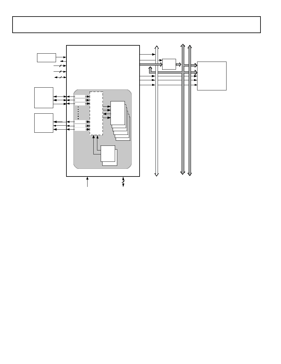
Figure 2 on Page 4
shows one sample configuration of a SPORT
using the precision clock generators to interface with an I
2
S
ADC and an I
2
S DAC with a much lower jitter clock than the
serial port would generate itself. Many other SRU configura-
tions are possible.
ADSP-21364 FAMILY CORE ARCHITECTURE
The ADSP-21364 is code compatible at the assembly level with
the ADSP-2126x, ADSP-21160 and ADSP-21161, and with the
first generation ADSP-2106x SHARC DSPs. The ADSP-21364
shares architectural features with the ADSP-2126x and
ADSP-2116x SIMD SHARC processors, as detailed in the fol-
lowing sections.
SIMD Computational Engine
The ADSP-21364 contains two computational processing ele-
ments that operate as a Single-Instruction Multiple-Data
(SIMD) engine. The processing elements are referred to as PEX
and PEY and each contains an ALU, multiplier, shifter and reg-
ister file. PEX is always active, and PEY may be enabled by
setting the PEYEN mode bit in the MODE1 register. When this
mode is enabled, the same instruction is executed in both pro-
cessing elements, but each processing element operates on
different data. This architecture is efficient at executing math
intensive signal processing algorithms.
Entering SIMD mode also has an effect on the way data is trans-
ferred between memory and the processing elements. When in
SIMD mode, twice the data bandwidth is required to sustain
computational operation in the processing elements. Because of
this requirement, entering SIMD mode also doubles the band-
width between memory and the processing elements. When
using the DAGs to transfer data in SIMD mode, two data values
are transferred with each access of memory or the register file.
Table 1. ADSP-21364 Benchmarks (at 333 MHz)
Benchmark Algorithm
Speed
(at 333 MHz)
1024 Point Complex FFT (Radix 4, with reversal) 27.9
µs
FIR Filter (per tap)
1
1
Assumes two files in multichannel SIMD mode
1.5 ns
IIR Filter (per biquad)
1
6.0 ns
Matrix Multiply (pipelined)
[3x3] × [3x1]
[4x4] × [4x1]
13.5 ns
23.9 ns
Divide (y/×)
10.5 ns
Inverse Square Root
16.3 ns
Rev. PrB
|
Page 4 of 52
|
September 2004
ADSP-21364
Preliminary Technical Data
Independent, Parallel Computation Units
Within each processing element is a set of computational units.
The computational units consist of an arithmetic/logic unit
(ALU), multiplier, and shifter. These units perform all opera-
tions in a single cycle. The three units within each processing
element are arranged in parallel, maximizing computational
throughput. Single multifunction instructions execute parallel
ALU and multiplier operations. In SIMD mode, the parallel
ALU and multiplier operations occur in both processing ele-
ments. These computation units support IEEE 32-bit single-
precision floating-point, 40-bit extended precision floating-
point, and 32-bit fixed-point data formats.
Data Register File
A general-purpose data register file is contained in each
processing element. The register files transfer data between the
computation units and the data buses, and store intermediate
results. These 10-port, 32-register (16 primary, 16 secondary)
register files, combined with the ADSP-2136x enhanced Har-
vard architecture, allow unconstrained data flow between
computation units and internal memory. The registers in PEX
are referred to as R0R15 and in PEY as S0S15.
Single-Cycle Fetch of Instruction and Four Operands
The ADSP-21364 features an enhanced Harvard architecture in
which the data memory (DM) bus transfers data and the pro-
gram memory (PM) bus transfers both instructions and data
(see
Figure 1 on Page 1
). With the ADSP-21364's separate pro-
gram and data memory buses and on-chip instruction cache,
the processor can simultaneously fetch four operands (two over
each data bus) and one instruction (from the cache), all in a sin-
gle cycle.
Instruction Cache
The ADSP-21364 includes an on-chip instruction cache that
enables three-bus operation for fetching an instruction and four
data values. The cache is selective--only the instructions whose
fetches conflict with PM bus data accesses are cached. This
cache allows full-speed execution of core, looped operations
such as digital filter multiply-accumulates, and FFT butterfly
processing.
Data Address Generators With Zero-Overhead Hardware
Circular Buffer Support
The ADSP-21364's two data address generators (DAGs) are
used for indirect addressing and implementing circular data
buffers in hardware. Circular buffers allow efficient program-
ming of delay lines and other data structures required in digital
Figure 2. ADSP-21364 System Sample Configuration
DAI
SPI
IDP
SRC
SPDI F
SPORT0-5
SCLK0
SD0A
SFS0
SD0B
SRU
DAI_P1
DAI_P2
DAI_P3
DAI_P18
DAI _P19
DAI_P20
DAC
(OPTI ONAL)
ADC
(OPTI ONAL)
FS
CLK
SDAT
FS
CLK
SDAT
3
CLOCK
FLAG3-1
2
2
CLKIN
XTAL
CLK_CFG1-0
BOOTCFG1-0
ADDR
PARALLEL
PORT
RAM, ROM
BOO T ROM
I /O DEVI CE
OE
DATA
WE
RD
WR
CLKOUT
ALE
AD15-0
LATCH
RESET
JTAG
6
ADSP-21364
AD
DRE
S
S
DA
T
A
CO
N
T
R
O
L
CS
FLAG0
PCG B
PCGA
CLK
FS
TIMERS
ADSP-21364
Preliminary Technical Data
Rev. PrB
|
Page 5 of 52
|
September 2004
signal processing, and are commonly used in digital filters and
Fourier transforms. The two DAGs of the ADSP-21364 contain
sufficient registers to allow the creation of up to 32 circular buff-
ers (16 primary register sets, 16 secondary). The DAGs
automatically handle address pointer wraparound, reduce over-
head, increase performance, and simplify implementation.
Circular buffers can start and end at any memory location.
Flexible Instruction Set
The 48-bit instruction word accommodates a variety of parallel
operations, for concise programming. For example, the
ADSP-21364 can conditionally execute a multiply, an add, and a
subtract in both processing elements while branching and fetch-
ing up to four 32-bit values from memory--all in a single
instruction.
ADSP-21364 MEMORY AND I/O INTERFACE
FEATURES
The ADSP-21364 adds the following architectural features to
the SIMD SHARC family core.
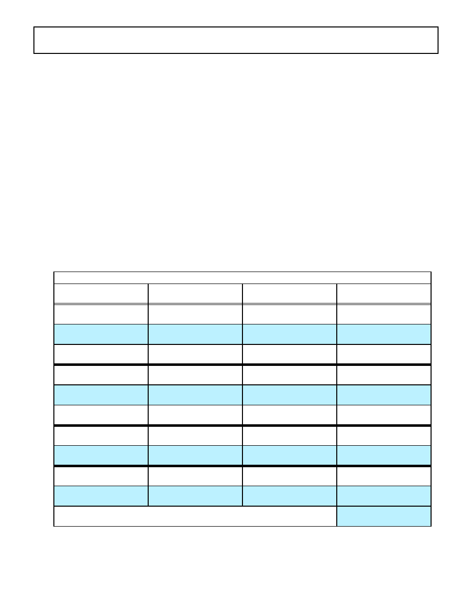
On-Chip Memory
The ADSP-21364 contains three megabits of internal SRAM.
Each block can be configured for different combinations of code
and data storage (see
Table 2 on Page 5
). Each memory block
supports single-cycle, independent accesses by the core proces-
sor and I/O processor. The ADSP-21364 memory architecture,
in combination with its separate on-chip buses, allow two data
transfers from the core and one from the I/O processor, in a sin-
gle cycle.
The ADSP-21364's, SRAM can be configured as a maximum of
96K words of 32-bit data, 192K words of 16-bit data, 64K words
of 48-bit instructions (or 40-bit data), or combinations of differ-
ent word sizes up to three megabits. All of the memory can be
accessed as 16-bit, 32-bit, 48-bit, or 64-bit words. A 16-bit float-
ing-point storage format is supported that effectively doubles
the amount of data that may be stored on-chip. Conversion
between the 32-bit floating-point and 16-bit floating-point for-
mats is performed in a single instruction. While each memory
block can store combinations of code and data, accesses are
most efficient when one block stores data using the DM bus for
transfers, and the other block stores instructions and data using
the PM bus for transfers.
Table 2. ADSP-21364 Internal Memory Space
IOP Registers 0x0000 0000 0003 FFFF
Long Word (64 bits)
Extended Precision Normal or
Instruction Word (48 bits)
Normal Word (32 bits)
Short Word (16 bits)
BLOCK 0 ROM
0x0004 0000 0x0004 7FFF
BLOCK 0 ROM
0x0008 00000x0008 AAAA
BLOCK 0 ROM
0x0008 0000 0x0008 FFFF
BLOCK 0 ROM
0x0010 00000x0011 FFFF
Reserved
0x0004 80000x0004 BFFF
Reserved
0x0009 00000x0009 7FFF
Reserved
0x0012 00000x0012 FFFF
BLOCK 0 RAM
0x0004 C0000x0004 FFFF
BLOCK 0 RAM
0x0009 00000x0009 5555
BLOCK 0 RAM
0x0009 80000x0009 FFFF
BLOCK 0 RAM
0x0013 00000x0013 FFFF
BLOCK 1 ROM
0x0005 00000x0005 7FFF
BLOCK 1 ROM
0x000A 00000x000A AAAA
BLOCK 1 ROM
0x000A 0000 0x000A FFFF
BLOCK 1 ROM
0x0014 00000x0015 FFFF
Reserved
0x0005 80000x0005 BFFF
Reserved
0x000B 00000x000B 7FFF
Reserved
0x0016 00000x0016 FFFF
BLOCK 1 RAM
0x0005 C0000x0005 FFFF
BLOCK 1 RAM
0x000B 00000x000B 5555
BLOCK 1 RAM
0x000B 80000x000B FFFF
BLOCK 1 RAM
0x0017 00000x0017 FFFF
BLOCK 2 RAM
0x0006 00000x0006 1FFF
BLOCK 2 RAM
0x000C 00000x000C 2AAA
BLOCK 2 RAM
0x000C 00000x000C 3FFF
BLOCK 2 RAM
0x0018 00000x0018 7FFF
Reserved
0x0006 20000x0006 FFFF
Reserved
0x000C 4000 0x000D FFFF
Reserved
0x0018 80000x001B FFFF
BLOCK 3 RAM
0x0007 00000x0007 1FFF
BLOCK 3 RAM
0x000E 00000x000E 2AAA
BLOCK 3 RAM
0x000E 00000x000E 3FFF
BLOCK 3 RAM
0x001C 00000x001C 7FFF
Reserved
0x0007 20000x0007 FFFF
Reserved
0x000E 40000x000F FFFF
Reserved
0x001C 80000x001F FFFF
Reserved
0x0020 00000xFFFF FFFF
Rev. PrB
|
Page 6 of 52
|
September 2004
ADSP-21364
Preliminary Technical Data
Using the DM bus and PM buses, with one dedicated to each
memory block assures single-cycle execution with two data
transfers. In this case, the instruction must be available in the
cache.
DMA Controller
The ADSP-21364's on-chip DMA controller allows data trans-
fers without processor intervention. The DMA controller
operates independently and invisibly to the processor core,
allowing DMA operations to occur while the core is simulta-
neously executing its program instructions. DMA transfers can
occur between the ADSP-21364's internal memory and its serial
ports, the SPI-compatible (Serial Peripheral Interface) ports, the
IDP (Input Data Port), the Parallel Data Acquisition Port
(PDAP), or the parallel port. Twenty-five channels of DMA are
available on the ADSP-21364--two for the SPI interface, two for
memory-to-memory transfers, twelve via the serial ports, eight
via the Input Data Port, and one via the processor's parallel
port. Programs can be downloaded to the ADSP-21364 using
DMA transfers. Other DMA features include interrupt genera-
tion upon completion of DMA transfers, and DMA chaining for
automatic linked DMA transfers.
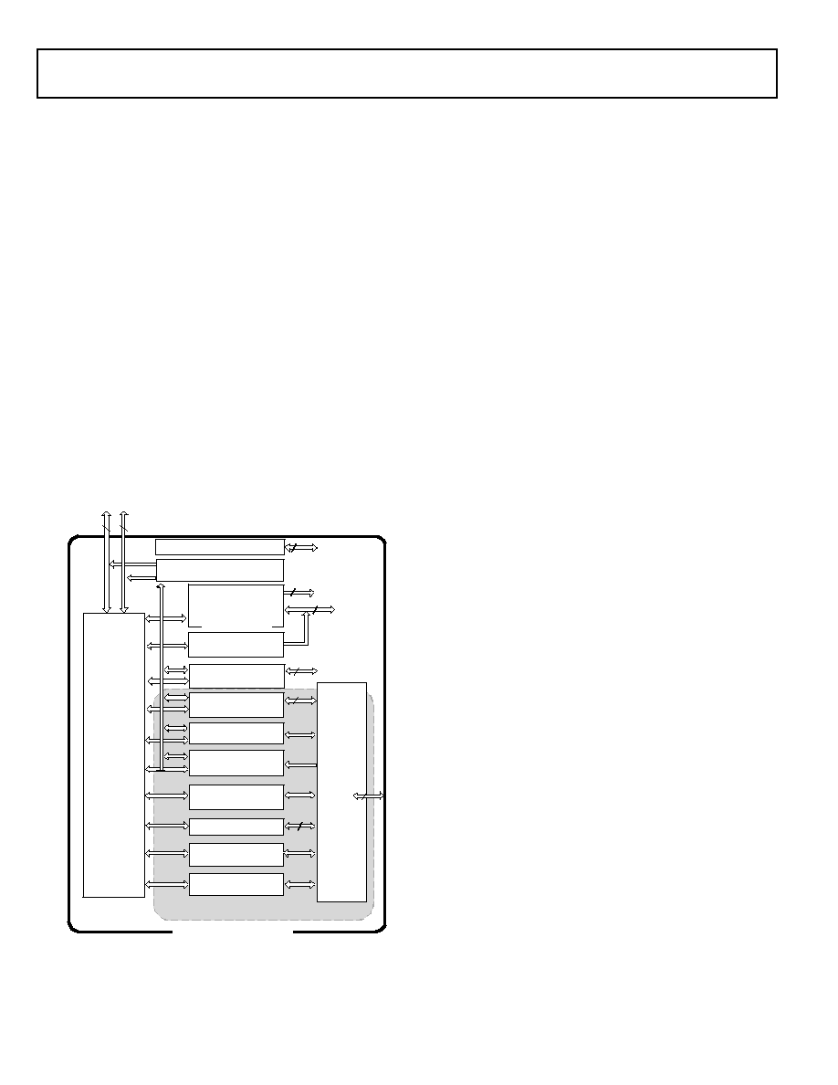
Digital Audio Interface (DAI)
The Digital Audio Interface (DAI) provides the ability to con-
nect various peripherals to any of the SHARCs DAI pins
(DAI_P201).
Programs make these connections using the Signal Routing
Unit (SRU, shown in
Figure 3
).
The SRU is a matrix routing unit (or group of multiplexers) that
enables the peripherals provided by the DAI to be intercon-
nected under software control. This allows easy use of the DAI
associated peripherals for a much wider variety of applications
by using a larger set of algorithms than is possible with noncon-
figurable signal paths.
The DAI also includes six serial ports, two precision clock gen-
erators (PCGs), eight channels of asynchronous sample rate
converters, an input data port (IDP), an SPI port, six flag out-
puts and six flag inputs, and three timers. The IDP provides an
additional input path to the ADSP-21364 core, configurable as
either eight channels of I
2
S serial data or as seven channels plus
a single 20-bit wide synchronous parallel data acquisition port.
Each data channel has its own DMA channel that is indepen-
dent from the ADSP-21364's serial ports.
For complete information on using the DAI, see the ADSP-
2136x SHARC Processor Hardware Reference.
Serial Ports
The ADSP-21364 features six synchronous serial ports that pro-
vide an inexpensive interface to a wide variety of digital and
mixed-signal peripheral devices such as Analog Devices'
AD183x family of audio codecs, ADCs, and DACs. The serial
ports are made up of two data lines, a clock and frame sync. The
data lines can be programmed to either transmit or receive and
each data line has a dedicated DMA channel.
Serial ports are enabled via 12 programmable and simultaneous
receive or transmit pins that support up to 24 transmit or 24
receive channels of audio data when all six SPORTS are enabled,
or six full duplex TDM streams of 128 channels per frame.
The serial ports operate at a maximum data rate of 50M bits/s.
Serial port data can be automatically transferred to and from
on-chip memory via dedicated DMA channels. Each of the
serial ports can work in conjunction with another serial port to
provide TDM support. One SPORT provides two transmit sig-
nals while the other SPORT provides the two receive signals.
The frame sync and clock are shared.
Serial ports operate in four modes:
· Standard DSP serial mode
· Multichannel (TDM) mode
· I
2
S mode
· Left-justified sample pair mode
Left-justified sample pair mode is a mode where in each frame
sync cycle two samples of data are transmitted/received--one
sample on the high segment of the frame sync, the other on the
low segment of the frame sync. Programs have control over var-
ious attributes of this mode.
Figure 3. ADSP-21364 I/O Processor and Peripherals Block Diagram
1 6
3
P RECI SIO N CLOCK
GENERATORS (2)
S PI P ORT (1 )
4
S ERIAL PORTS (6 )
INPUT
DATA P ORTS (8 )
TI ME RS (3)
3
DMA CONTROLLER
IOP
R
E
GI
S
T
E
R
S
(
M
E
M
O
R
Y
M
AP
P
E
D)
C
O
N
TR
O
L,
S
TA
T
U
S
,
&
D
A
TA
B
U
FFE
R
S
I/O PROCESSOR
P ARALLEL PO RT
4
GPI O FLAGS/I RQ/TIMEXP
S
I
G
N
AL
RO
U
T
I
N
G
U
NI
T
A D D RE SS /D AT A B U S/ G P IO
CO N T R O L /G PIO
DIGITAL AUDIO INTERFACE
2 5 C H A N NE LS
TO PROCES SOR BUSS ES AND
SYS TE M ME MO RY
IO ADDRE SS
BUS (18 )
PW M (1 6)
IO DATA
BUS (32 )
SPI PORT (1)
4
20
SRC (8 CHANNELS)
SPDIF (RX/ TX )

ADSP-21364
Preliminary Technical Data
Rev. PrB
|
Page 7 of 52
|
September 2004
Each of the serial ports supports the left-justified sample pair
and I
2
S protocols (I
2
S is an industry standard interface com-
monly used by audio codecs, ADCs and DACs such as the
Analog Devices AD183x family), with two data pins, allowing
four left-justified sample pair or I
2
S channels (using two stereo
devices) per serial port, with a maximum of up to 24 I
2
S chan-
nels. The serial ports permit little-endian or big-endian
transmission formats and word lengths selectable from 3 bits to
32 bits. For the left-justified sample pair and I
2
S modes, data-
word lengths are selectable between 8 bits and 32 bits. Serial
ports offer selectable synchronization and transmit modes as
well as optional µ-law or A-law companding selection on a per
channel basis. Serial port clocks and frame syncs can be inter-
nally or externally generated.
Parallel Port
The Parallel Port provides interfaces to SRAM and peripheral
devices. The multiplexed address and data pins (AD150) can
access 8-bit devices with up to 24 bits of address, or 16-bit
devices with up to 16 bits of address. In either mode, 8- or 16-
bit, the maximum data transfer rate is 55M bytes/sec.
DMA transfers are used to move data to and from internal
memory. Access to the core is also facilitated through the paral-
lel port register read/write functions. The RD, WR, and ALE
(Address Latch Enable) pins are the control pins for the parallel
port.
Serial Peripheral (Compatible) Interface
The ADSP-21364 SHARC processor contains two Serial Periph-
eral Interface ports (SPIs). The SPI is an industry standard
synchronous serial link, enabling the ADSP-21364 SPI compati-
ble port to communicate with other SPI compatible devices. The
SPI consists of two data pins, one device select pin, and one
clock pin. It is a full-duplex synchronous serial interface, sup-
porting both master and slave modes. The SPI port can operate
in a multimaster environment by interfacing with up to four
other SPI compatible devices, either acting as a master or slave
device. The ADSP-21364 SPI compatible peripheral implemen-
tation also features programmable baud rate and clock phase
and polarities. The ADSP-21364 SPI compatible port uses open
drain drivers to support a multimaster configuration and to
avoid data contention.
The sample rate converter (SRC) contains four SRC blocks and
is the same core as that used in the AD1896 192 kHz Stereo
Asynchronous Sample Rate Converter providing up to 140dB
SNR. The SRC block is used to perform synchronous or asyn-
chronous sample rate conversion across independent stereo
channels, without using internal processor resources. The four
SRC blocks can also be configured to operate together to con-
vert multichannel audio data without phase mismatches.
Finally, the SRC is used to clean up audio data from jittery clock
sources such as the S/PDIF receiver.
S/PDIF Compatible Digital Audio Receiver/Transmitter
and Synchronous/Asynchronous Sample Rate Converter
The S/PDIF transmitter has no separate DMA channels. It
receives audio data in serial format and converts it into a
biphase encoded signal. The serial data input to the transmitter
can be formatted as left justified, I
2
S or right justified with word
widths of 16, 18, 20, or 24 bits.
The serial data, clock, and frame sync inputs to the S/PDIF
transmitter are routed through the Signal Routing Unit (SRU).
They can come from a variety of sources such as the SPORTs,
external pins, the precision clock generators (PCGs), or the
sample rate converters (SRC) and are controlled by the SRU
control registers.
The sample rate converter (SRC) contains four SRC blocks and
is the same core as that used in the AD1896 192 kHz Stereo
Asynchronous Sample Rate Converter providing up to 140dB
SNR. The SRC block is used to perform synchronous or asyn-
chronous sample rate conversion across independent stereo
channels, without using internal processor resources. The four
SRC blocks can also be configured to operate together to con-
vert multichannel audio data without phase mismatches.
Finally, the SRC is used to clean up audio data from jittery clock
sources such as the S/PDIF receiver.
Pulse Width Modulation
The PWM module is a flexible, programmable, PWM waveform
generator that can be programmed to generate the required
switching patterns for various applications related to motor and
engine control or audio power control. The PWM generator can
generate either center-aligned or edge-aligned PWM wave-
forms. In addition, it can generate complementary signals on
two outputs in paired mode or independent signals in non-
paired mode (applicable to a single group of four PWM
waveforms).
The entire PWM module has four groups of four PWM outputs
each. Therefore this module generates 16 PWM outputs in total.
Each PWM group produces two pairs of PWM signals on the
four PWM outputs.
The PWM generator is capable of operating in two distinct
modes while generating center-aligned PWM waveforms: single
update mode, or double update mode. In single update mode
the duty cycle values are programmable only once per PWM
period. This results in PWM patterns that are symmetrical
around the mid-point of the PWM period. In double update
mode, a second updating of the PWM registers is implemented
at the mid-point of the PWM period. In this mode, it is possible
to produce asymmetrical PWM patterns that produce lower
harmonic distortion in three-phase PWM inverters.
Rev. PrB
|
Page 8 of 52
|
September 2004
ADSP-21364
Preliminary Technical Data
Timers
The ADSP-21364 has a total of four timers: a core timer able to
generate periodic software interrupts and three general purpose
timers that can generate periodic interrupts and be indepen-
dently set to operate in one of three modes:
· Pulse Waveform Generation mode
· Pulse Width Count /Capture mode
· External Event Watchdog mode
The core timer can be configured to use FLAG3 as a Timer
Expired signal, and each general-purpose timer has one bidirec-
tional pin and four registers that implement its mode of
operation: a 6-bit configuration register, a 32-bit count register,
a 32-bit period register, and a 32-bit pulse width register. A sin-
gle control and status register enables or disables all three
general purpose timers independently.
Program Booting
The internal memory of the ADSP-21364 boots at system
power-up from an 8-bit EPROM via the parallel port, an SPI
master, an SPI slave or an internal boot. Booting is determined
by the Boot Configuration (BOOTCFG10) pins (see
Table 6 on
Page 14
). Selection of the boot source is controlled via the SPI as
either a master or slave device.
Phase-Locked Loop
The ADSP-21364 uses an on-chip Phase-Locked Loop (PLL) to
generate the internal clock for the core. On power up, the
CLKCFG10 pins are used to select ratios of 32:1, 16:1, and 6:1
(see
Table 7 on Page 14
). After booting, numerous other ratios
can be selected via software control. The ratios are made up of
software configurable numerator values from 1 to 32 and soft-
ware configurable divisor values of 1, 2, 4, 8, and 16.
Power Supplies
The ADSP-21364 has separate power supply connections for the
internal (V
DDINT
), external (V
DDEXT
), and analog (A
VDD
/A
VSS
)
power supplies. The internal and analog supplies must meet the
1.2 V requirement. The external supply must meet the 3.3 V
requirement. All external supply pins must be connected to the
same power supply.
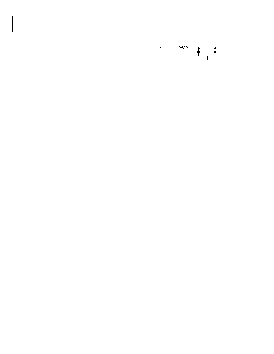
Note that the analog supply (A
VDD
) powers the ADSP-21364's
clock generator PLL. To produce a stable clock, programs
should provide an external circuit to filter the power input to
the A
VDD
pin. Place the filter as close as possible to the pin. For
an example circuit, see
Figure 4
. To prevent noise coupling, use
a wide trace for the analog ground (A
VSS
) signal and install a
decoupling capacitor as close as possible to the pin. Note that
the A
VSS
and A
VDD
pins specified in
Figure 4
are inputs to the
processor and not the analog ground plane on the board.
Target Board JTAG Emulator Connector
Analog Devices DSP Tools product line of JTAG emulators uses
the IEEE 1149.1 JTAG test access port of the ADSP-21364 pro-
cessor to monitor and control the target board processor during
emulation. Analog Devices DSP Tools product line of JTAG
emulators provides emulation at full processor speed, allowing
inspection and modification of memory, registers, and proces-
sor stacks. The processor's JTAG interface ensures that the
emulator will not affect target system loading or timing.
For complete information on Analog Devices' SHARC DSP
Tools product line of JTAG emulator operation, see the appro-
priate "Emulator Hardware User's Guide".
DEVELOPMENT TOOLS
The ADSP-21364 is supported with a complete set of
CROSSCORE® software and hardware development tools,
including Analog Devices emulators and VisualDSP++® devel-
opment environment. The same emulator hardware that
supports other SHARC processors also fully emulates the
ADSP-21364.
The VisualDSP++ project management environment lets pro-
grammers develop and debug an application. This environment
includes an easy to use assembler (which is based on an alge-
braic syntax), an archiver (librarian/library builder), a linker, a
loader, a cycle-accurate instruction-level simulator, a C/C++
compiler, and a C/C++ runtime library that includes DSP and
mathematical functions. A key point for these tools is C/C++
code efficiency. The compiler has been developed for efficient
translation of C/C++ code to DSP assembly. The SHARC has
architectural features that improve the efficiency of compiled
C/C++ code.
The VisualDSP++ debugger has a number of important fea-
tures. Data visualization is enhanced by a plotting package that
offers a significant level of flexibility. This graphical representa-
tion of user data enables the programmer to quickly determine
the performance of an algorithm. As algorithms grow in com-
plexity, this capability can have increasing significance on the
designer's development schedule, increasing productivity. Sta-
tistical profiling enables the programmer to non intrusively poll
the processor as it is running the program. This feature, unique
to VisualDSP++, enables the software developer to passively
gather important code execution metrics without interrupting
the real-time characteristics of the program. Essentially, the
developer can identify bottlenecks in software quickly and effi-
ciently. By using the profiler, the programmer can focus on
those areas in the program that impact performance and take
corrective action.
Debugging both C/C++ and assembly programs with the
VisualDSP++ debugger, programmers can:
· View mixed C/C++ and assembly code (interleaved source
and object information)
· Insert breakpoints
Figure 4. Analog Power (A
VDD
) Filter Circuit
V
DDINT
A
VDD
A
VSS
0.01 F
0.1 F
10

ADSP-21364
Preliminary Technical Data
Rev. PrB
|
Page 9 of 52
|
September 2004
· Set conditional breakpoints on registers, memory,
and stacks
· Trace instruction execution
· Perform linear or statistical profiling of program execution
· Fill, dump, and graphically plot the contents of memory
· Perform source level debugging
· Create custom debugger windows
The VisualDSP++ IDDE lets programmers define and manage
DSP software development. Its dialog boxes and property pages
let programmers configure and manage all of the SHARC devel-
opment tools, including the color syntax highlighting in the
VisualDSP++ editor. This capability permits programmers to:
· Control how the development tools process inputs and
generate outputs
· Maintain a one-to-one correspondence with the tool's
command line switches
The VisualDSP++ Kernel (VDK) incorporates scheduling and
resource management tailored specifically to address the mem-
ory and timing constraints of DSP programming. These
capabilities enable engineers to develop code more effectively,
eliminating the need to start from the very beginning, when
developing new application code. The VDK features include
Threads, Critical and Unscheduled regions, Semaphores,
Events, and Device flags. The VDK also supports Priority-based,
Preemptive, Cooperative, and Time-Sliced scheduling
approaches. In addition, the VDK was designed to be scalable. If
the application does not use a specific feature, the support code
for that feature is excluded from the target system.
Because the VDK is a library, a developer can decide whether to
use it or not. The VDK is integrated into the VisualDSP++
development environment, but can also be used via standard
command line tools. When the VDK is used, the development
environment assists the developer with many error-prone tasks
and assists in managing system resources, automating the gen-
eration of various VDK based objects, and visualizing the
system state, when debugging an application that uses the VDK.
VisualDSP++ Component Software Engineering (VCSE) is
Analog Devices' technology for creating, using, and reusing
software components (independent modules of substantial
functionality) to quickly and reliably assemble software applica-
tions. Download components from the Web and drop them into
the application. Publish component archives from within Visu-
alDSP++. VCSE supports component implementation in
C/C++ or assembly language.
Use the Expert Linker to visually manipulate the placement of
code and data on the embedded system. View memory utiliza-
tion in a color-coded graphical form, easily move code and data
to different areas of the processor or external memory with the
drag of the mouse, examine run time stack and heap usage. The
Expert Linker is fully compatible with the existing Linker Defi-
nition File (LDF), allowing the developer to move between the
graphical and textual environments.
In addition to the software and hardware development tools
available from Analog Devices, third parties provide a wide
range of tools supporting the SHARC processor family. Hard-
ware tools include SHARC processor PC plug-in cards. Third
party software tools include DSP libraries, real-time operating
systems, and block diagram design tools.
Designing an Emulator-Compatible DSP Board (Target)
The Analog Devices family of emulators are tools that every
developer needs to test and debug hardware and software sys-
tems. Analog Devices has supplied an IEEE 1149.1 JTAG Test
Access Port (TAP) on each JTAG DSP. Nonintrusive in-circuit
emulation is assured by the use of the processor's JTAG inter-
face--the emulator does not affect target system loading or
timing. The emulator uses the TAP to access the internal fea-
tures of the processor, allowing the developer to load code, set
breakpoints, observe variables, observe memory, and examine
registers. The processor must be halted to send data and com-
mands, but once an operation has been completed by the
emulator, the processor system is set running at full speed with
no impact on system timing.
To use these emulators, the target board must include a header
that connects the processor's JTAG port to the emulator.
For details on target board design issues including mechanical
layout, single processor connections, multiprocessor scan
chains, signal buffering, signal termination, and emulator pod
logic, see the EE-68: Analog Devices JTAG Emulation Technical
Reference on the Analog Devices website (
www.analog.com
)--
use site search on "EE-68." This document is updated regularly
to keep pace with improvements to emulator support.
Evaluation Kit
Analog Devices offers a range of EZ-KIT Lite evaluation plat-
forms to use as a cost effective method to learn more about
developing or prototyping applications with Analog Devices
processors, platforms, and software tools. Each EZ-KIT Lite
includes an evaluation board along with an evaluation suite of
the VisualDSP++ development and debugging environment
with the C/C++ compiler, assembler, and linker. Also included
are sample application programs, power supply, and a USB
cable. All evaluation versions of the software tools are limited
for use only with the EZ-KIT Lite product.
The USB controller on the EZ-KIT Lite board connects the
board to the USB port of the user's PC, enabling the Visu-
alDSP++ evaluation suite to emulate the on-board processor in-
circuit. This permits the customer to download, execute, and
debug programs for the EZ-KIT Lite system. It also allows in-
circuit programming of the on-board Flash device to store user-
specific boot code, enabling the board to run as a standalone
unit without being connected to the PC.
With a full version of VisualDSP++ installed (sold separately),
engineers can develop software for the EZ-KIT Lite or any cus-
tom defined system. Connecting one of Analog Devices JTAG
emulators to the EZ-KIT Lite board enables high-speed, non-
intrusive emulation.

Rev. PrB
|
Page 10 of 52
|
September 2004
ADSP-21364
Preliminary Technical Data
ADDITIONAL INFORMATION
This data sheet provides a general overview of the ADSP-21364
architecture and functionality. For detailed information on the
ADSP-2136x Family core architecture and instruction set, refer
to the ADSP-2136x SHARC Processor Hardware Reference and
the ADSP-2136x SHARC Processor Programming Reference.
ADSP-21364
Preliminary Technical Data
Rev. PrB
|
Page 11 of 52
|
September 2004
PIN FUNCTION DESCRIPTIONS
ADSP-21364 pin definitions are listed below. Inputs identified
as synchronous (S) must meet timing requirements with respect
to CLKIN (or with respect to TCK for TMS and TDI). Inputs
identified as asynchronous (A) can be asserted asynchronously
to CLKIN (or to TCK for TRST). Tie or pull unused inputs to
V
DDEXT
or GND, except for the following:
· DAI_Px, SPICLK, MISO, MOSI, EMU, TMS, TRST, TDI,
and AD150 (NOTE: These pins have pullup resistors.)
The following symbols appear in the Type column of
Table 3
:
A = Asynchronous, G = Ground, I = Input, O = Output,
P = Power Supply, S = Synchronous, (A/D) = Active Drive,
(O/D) = Open Drain, and T = Three-State, (pd) = pulldown
resistor, (pu) = pullup resistor. .
Table 3. Pin Descriptions
Pin Type
State
During
&
After Reset
Function
AD150
I/O/T
(pu)
Three-state with
pullup enabled
Parallel Port Address/Data. The ADSP-21364 parallel port and its corresponding
DMA unit output addresses and data for peripherals on these multiplexed pins. The
multiplex state is determined by the ALE pin. The parallel port can operate in either
8-bit or 16-bit mode. Each AD pin has a 22.5 k
internal pullup resistor. See
Address
Data Modes on Page 14
for details of the AD pin operation.
For 8-bit mode: ALE is automatically asserted whenever a change occurs in the upper
16 external address bits, A238; ALE is used in conjunction with an external latch to
retain the values of the A238.
For 16-bit mode: ALE is automatically asserted whenever a change occurs in the
address bits, A150; ALE is used in conjunction with an external latch to retain the
values of the A150. To use these pins as flags (FLAGS150) or PWMs (PWM150), 1)
set (=1) bit 20 of the SYSCTL register to disable the parallel port, 2) set (=1) bits 2225
of the SYSCTL register to enable FLAGS in groups of four (bit 22 for FLAGS30, bit 23
for FLAGS74 etc.) or, set (=1) bits 2629 of the SYSCTL register to enable PWMs in
groups of four (bit 26 for PWM03, bit 27 for PWM47, and so on). When used as an
input, the IDP Channel0 can use these pins for parallel input data.
RD
O
(pu)
Three-state, driven
high
1
Parallel Port Read Enable. RD is asserted low whenever the processor reads 8-bit or
16-bit data from an external memory device. When AD150 are flags, this pin remains
deasserted. RD has a 22.5 k
internal pullup resistor.
WR
O
(pu)
Three-state, driven
high
1
Parallel Port Write Enable. WR is asserted low whenever the processor writes 8-bit or
16-bit data to an external memory device. When AD150 are flags, this pin remains
deasserted. WR has a 22.5 k
internal pullup resistor.
ALE
O
(pd)
Three-state, driven
low
1
Parallel Port Address Latch enable. ALE is asserted whenever the processor drives
a new address on the parallel port address pins. On reset, ALE is active high. However,
it can be reconfigured using software to be active low. When AD150 are flags, this
pin remains deasserted. ALE has a 20 k
internal pulldown resistor.
FLAG30
I/O/A
Three-state
Flag Pins. Each flag pin is configured via control bits as either an input or output. As
an input, it can be tested as a condition. As an output, it can be used to signal external
peripherals. These pins can be used as an SPI interface slave select output during SPI
mastering. These pins are also multiplexed with the IRQx and the TIMEXP signals.
In SPI master boot mode, FLAG0 is the slave select pin that must be connected to an
SPI EPROM. FLAG0 is configured as a slave select during SPI master boot. When bit 16
is set (=1) in the SYSCTL register, FLAG0 is configured as IRQ0.
When bit 17 is set (=1) in the SYSCTL register, FLAG1 is configured as IRQ1.
When bit 18 is set (=1) in the SYSCTL register, FLAG2 is configured as IRQ2.
When bit 19 is set (=1) in the SYSCTL register, FLAG3 is configured as TIMEXP which
indicates that the system timer has expired.
Rev. PrB
|
Page 12 of 52
|
September 2004
ADSP-21364
Preliminary Technical Data
DAI_P201
I/O/T
(pu)
Three-state with
programmable
pullup
Digital Audio Interface Pins. These pins provide the physical interface to the SRU.
The SRU configuration registers define the combination of on-chip peripheral inputs
or outputs connected to the pin and to the pin's output enable. The configuration
registers of these peripherals then determines the exact behavior of the pin. Any input
or output signal present in the SRU may be routed to any of these pins. The SRU
provides the connection from the Serial ports, Input data port, precision clock gener-
ators and timers, sample rate converters and SPI to the DAI_P201 pins These pins
have internal 22.5 k
pullup resistors which are enabled on reset. These pullups can
be disabled in the DAI_PIN_PULLUP register.
SPICLK
I/O
(pu)
Three-state with
pullup enabled
Serial Peripheral Interface Clock Signal. Driven by the master, this signal controls
the rate at which data is transferred. The master may transmit data at a variety of baud
rates. SPICLK cycles once for each bit transmitted. SPICLK is a gated clock that is active
during data transfers, only for the length of the transferred word. Slave devices ignore
the serial clock if the slave select input is driven inactive (HIGH). SPICLK is used to shift
out and shift in the data driven on the MISO and MOSI lines. The data is always shifted
out on one clock edge and sampled on the opposite edge of the clock. Clock polarity
and clock phase relative to data are programmable into the SPICTL control register
and define the transfer format. SPICLK has a 22.5 k
internal pullup resistor.
SPIDS
I
Input only
Serial Peripheral Interface Slave Device Select. An active low signal used to select
the processor as an SPI slave device. This input signal behaves like a chip select, and
is provided by the master device for the slave devices. In multimaster mode the DSPs
SPIDS signal can be driven by a slave device to signal to the processor (as SPI master)
that an error has occurred, as some other device is also trying to be the master device.
If asserted low when the device is in master mode, it is considered a multimaster error.
For a single-master, multiple-slave configuration where flag pins are used, this pin
must be tied or pulled high to V
DDEXT
on the master device. For ADSP-21364 to
ADSP-21364 SPI interaction, any of the master ADSP-21364's flag pins can be used to
drive the SPIDS signal on the ADSP-21364 SPI slave device.
MOSI
I/O (O/D)
(pu)
Three-state with
pullup enabled
SPI Master Out Slave In. If the ADSP-21364 is configured as a master, the MOSI pin
becomes a data transmit (output) pin, transmitting output data. If the ADSP-21364 is
configured as a slave, the MOSI pin becomes a data receive (input) pin, receiving input
data. In an ADSP-21364 SPI interconnection, the data is shifted out from the MOSI
output pin of the master and shifted into the MOSI input(s) of the slave(s). MOSI has a
22.5 k
internal pullup resistor.
MISO
I/O (O/D)
(pu)
Three-state with
pullup enabled
SPI Master In Slave Out. If the ADSP-21364 is configured as a master, the MISO pin
becomes a data receive (input) pin, receiving input data. If the ADSP-21364 is
configured as a slave, the MISO pin becomes a data transmit (output) pin, transmitting
output data. In an ADSP-21364 SPI interconnection, the data is shifted out from the
MISO output pin of the slave and shifted into the MISO input pin of the master. MISO
has a 22.5 k
internal pullup resistor. MISO can be configured as O/D by setting the
OPD bit in the SPICTL register.
Note: Only one slave is allowed to transmit data at any given time. To enable broadcast
transmission to multiple SPI-slaves, the processor's MISO pin may be disabled by
setting (=1) bit 5 (DMISO) of the SPICTL register.
BOOTCFG10
I
Input only
Boot Configuration Select. This pin is used to select the boot mode for the processor.
The BOOTCFG pins must be valid before reset is asserted. See
Table 6
for a description
of the boot modes.
Table 3. Pin Descriptions (Continued)
Pin Type
State
During
&
After Reset
Function
ADSP-21364
Preliminary Technical Data
Rev. PrB
|
Page 13 of 52
|
September 2004
CLKIN
I
Input only
Local Clock In. Used in conjunction with XTAL. CLKIN is the ADSP-21364 clock input.
It configures the ADSP-21364 to use either its internal clock generator or an external
clock source. Connecting the necessary components to CLKIN and XTAL enables the
internal clock generator. Connecting the external clock to CLKIN while leaving XTAL
unconnected configures the ADSP-21364 to use the external clock source such as an
external clock oscillator. The core is clocked either by the PLL output or this clock input
depending on the CLKCFG10 pin settings. CLKIN may not be halted, changed, or
operated below the specified frequency.
XTAL
O
Output only
2
Crystal Oscillator Terminal. Used in conjunction with CLKIN to drive an external
crystal.
CLKCFG10
I
Input only
Core/CLKIN Ratio Control. These pins set the start up clock frequency. See
Table 7
for a description of the clock configuration modes.
Note that the operating frequency can be changed by programming the PLL multiplier
and divider in the PMCTL register at any time after the core comes out of reset.
RSTOUT/CLKOUT O
Output only
Local Clock Out/ Reset Out. Drives out the core reset signal to an external device.
CLKOUT can also be configured as a reset out pin.The functionality can be switched
between the PLL output clock and reset out by setting bit 12 of the PMCTREG register.
The default is reset out.
RESET
I/A
Input only
Processor Reset. Resets the ADSP-21364 to a known state. Upon deassertion, there
is a 4096 CLKIN cycle latency for the PLL to lock. After this time, the core begins
program execution from the hardware reset vector address. The RESET input must be
asserted (low) at power-up.
TCK
I
Input only
3
Test Clock (JTAG). Provides a clock for JTAG boundary scan. TCK must be asserted
(pulsed low) after power-up or held low for proper operation of the ADSP-21364.
TMS
I/S
(pu)
Three-state with
pullup enabled
Test Mode Select (JTAG). Used to control the test state machine. TMS has a 22.5 k
internal pullup resistor.
TDI
I/S
(pu)
Three-state with
pullup enabled
Test Data Input (JTAG). Provides serial data for the boundary scan logic. TDI has a
22.5 k
internal pullup resistor.
TDO
O
Three-state
4
Test Data Output (JTAG). Serial scan output of the boundary scan path.
TRST
I/A
(pu)
Three-state with
pullup enabled
Test Reset (JTAG). Resets the test state machine. TRST must be asserted (pulsed low)
after power-up or held low for proper operation of the ADSP-21364. TRST has a
22.5 k
internal pullup resistor.
EMU
O (O/D)
(pu)
Three-state with
pullup enabled
Emulation Status. Must be connected to the ADSP-21364 Analog Devices processor
Tools product line of JTAG emulators target board connector only. EMU has a 22.5 k
internal pullup resistor.
V
DDINT
P
Core Power Supply. Nominally +1.2 V dc and supplies the processor's core processor
(13 pins on the Mini-BGA package, 32 pins on the LQFP package).
V
DDEXT
P
I/O Power Supply. Nominally +3.3 V dc. (6 pins on the Mini-BGA package, 10 pins on
the LQFP package).
A
VDD
P
Analog Power Supply. Nominally +1.2 V dc and supplies the processor's internal PLL
(clock generator). This pin has the same specifications as V
DDINT
, except that added
filtering circuitry is required.
For more information, see Power Supplies on Page 8.
A
VSS
G
Analog Power Supply Return.
GND
G
Power Supply Return. (54 pins on the Mini-BGA package, 39 pins on the LQFP
package).
1
RD, WR, and ALE are three-stated (and not driven) only when RESET is active.
2
Output only is a three-state driver with its output path always enabled.
3
Input only is a three-state driver with both output path and pullup disabled.
4
Three-state is a three-state driver with pullup disabled.
Table 3. Pin Descriptions (Continued)
Pin Type
State
During
&
After Reset
Function
Rev. PrB
|
Page 14 of 52
|
September 2004
ADSP-21364
Preliminary Technical Data
ADDRESS DATA PINS AS FLAGS
To use these pins as flags (FLAGS150) set (=1) bit 20 of the
SYSCTL register to disable the parallel port. Then set (=1) bits
22 to 25 in the SYSCTL register accordingly.
ADDRESS DATA MODES
The following table shows the functionality of the AD pins for
8-bit and 16-bit transfers to the parallel port. For 8-bit data
transfers, ALE latches address bits A23A8 when asserted, fol-
lowed by address bits A7A0 and data bits D7D0 when
deasserted. For 16-bit data transfers, ALE latches address bits
A15A0 when asserted, followed by data bits D15D0 when
deasserted.
BOOT MODES
CORE INSTRUCTION RATE TO CLKIN RATIO MODES
For details on processor timing, see
Timing Specifications
and
Figure 5
on Page 17
.
Table 4. AD150 to Flag Pin Mapping
AD Pin
Flag Pin
AD Pin
Flag Pin
AD0
FLAG8
AD8
FLAG0
AD1
FLAG9
AD9
FLAG1
AD2
FLAG10
AD10
FLAG2
AD3
FLAG11
AD11
FLAG3
AD4
FLAG12
AD12
FLAG4
AD5
FLAG13
AD13
FLAG5
AD6
FLAG14
AD14
FLAG6
AD7
FLAG15
AD15
FLAG7
Table 5. Address/ Data Mode Selection
EP Data
Mode
ALE
AD70
Function
AD158
Function
8-bit
Asserted
A158
A2316
8-bit
Deasserted
D70
A70
16-bit
Asserted
A70
A158
16-bit
Deasserted
D70
D158
Table 6. Boot Mode Selection
BOOTCFG10
Booting Mode
00
SPI Slave Boot
01
SPI Master Boot
10
Parallel Port boot via EPROM
Table 7. Core Instruction Rate/ CLKIN Ratio Selection
CLKCFG10
Core to CLKIN Ratio
00
6:1
01
32:1
10
16:1
ADSP-21364
Preliminary Technical Data
Rev. PrB
|
Page 15 of 52
|
September 2004
ADSP-21364 SPECIFICATIONS
RECOMMENDED OPERATING CONDITIONS
ELECTRICAL CHARACTERISTICS
Parameter
1
1
Specifications subject to change without notice.
K Grade
B Grade
C Grade
Min
Max
Min
Max
Min
Max
Unit
V
DDINT
Internal (Core) Supply Voltage
1.14
1.26
1.14
1.26
0.95
1.05
V
A
VDD
Analog (PLL) Supply Voltage
1.14
1.26
1.14
1.26
0.95
1.05
V
V
DDEXT
External (I/O) Supply Voltage
3.13
3.47
3.13
3.47
3.13
3.47
V
V
IH
2
2
Applies to input and bidirectional pins: AD150, FLAG30, DAI_Px, SPICLK, MOSI, MISO, SPIDS, BOOTCFGx, CLKCFGx, RESET, TCK, TMS, TDI, TRST.
High Level Input Voltage @ V
DDEXT
= max
2.0
V
DDEXT
+ 0.5
2.0
V
DDEXT
+ 0.5
2.0
V
DDEXT
+ 0.5
V
V
IL
2
Low Level Input Voltage @ V
DDEXT
= min
0.5
+0.8
0.5
+0.8
0.5
+0.8
V
V
IH_CLKIN
3
3
Applies to input pin CLKIN.
High Level Input Voltage @ V
DDEXT
= max
1.74
V
DDEXT
+ 0.5
1.74
V
DDEXT
+ 0.5
1.74
V
DDEXT
+ 0.5
V
V
IL_CLKIN
Low Level Input Voltage @ V
DDEXT
= min
0.5
+1.19
0.5
+1.19
0.5
+1.19
V
T
AMB
4,
5
4
See
Thermal Characteristics on Page 44
for information on thermal specifications.
5
See Engineer-to-Engineer Note (No. TBD) for further information.
Ambient Operating Temperature
0
+70
40
+85
40
+105
°C
Parameter
1
Test Conditions
Min
Max
Unit
V
OH
2
High Level Output Voltage
@ V
DDEXT
= min, I
OH
= 1.0 mA
3
2.4
V
V
OL
2
Low Level Output Voltage
@ V
DDEXT
= min, I
OL
= 1.0 mA
3
0.4
V
I
IH
4, 5
High Level Input Current
@ V
DDEXT
= max, V
IN
= V
DDEXT
max
10
µA
I
IL
4
Low Level Input Current
@ V
DDEXT
= max, V
IN
= 0 V
10
µA
I
ILPU
5
Low Level Input Current Pullup
@ V
DDEXT
= max, V
IN
= 0 V
200
µA
I
OZH
6, 7
Three-State Leakage Current
@ V
DDEXT
= max, V
IN
= V
DDEXT
max
10
µA
I
OZL
6
Three-State Leakage Current
@ V
DDEXT
= max, V
IN
= 0 V
10
µA
I
OZLPU
7
Three-State Leakage Current Pullup
@ V
DDEXT
= max, V
IN
= 0 V
200
µA
I
DD-INTYP
8, 9
Supply Current (Internal)
t
CCLK
= min, V
DDINT
= nom
500
mA
AI
DD
10
Supply Current (Analog)
A
VDD
= max
10
mA
C
IN
11,
12
Input Capacitance
f
IN
=1 MHz, T
CASE
=25°C, V
IN
=1.2V
4.7
pF
1
Specifications subject to change without notice.
2
Applies to output and bidirectional pins: AD150, RD, WR, ALE, FLAG30, DAI_Px, SPICLK, MOSI, MISO, EMU, TDO, CLKOUT, XTAL.
3
See
Output Drive Currents on Page 43
for typical drive current capabilities.
4
Applies to input pins: SPIDS, BOOTCFGx, CLKCFGx, TCK, RESET, CLKIN.
5
Applies to input pins with 22.5 k internal pullups: TRST, TMS, TDI.
6
Applies to three-statable pins: FLAG30.
7
Applies to three-statable pins with 22.5 k pullups: AD15-0, DAI_Px, SPICLK, EMU, MISO, MOSI.
8
Typical internal current data reflects nominal operating conditions.
9
See Engineer-to-Engineer Note (No. TBD) for further information.
10
Characterized, but not tested.
11
Applies to all signal pins.
12
Guaranteed, but not tested.
Rev. PrB
|
Page 16 of 52
|
September 2004
ADSP-21364
Preliminary Technical Data
MAXIMUM POWER DISSIPATION
The data in this table is based on theta JA (
JA
) established per
JEDEC standards JESD51-2 and JESD51-6. See Engineer-to-
Engineer note (EE-TBD) for further information. For informa-
tion on package thermal specifications, see
Thermal
Characteristics on Page 44
.
ABSOLUTE MAXIMUM RATINGS
ESD SENSITIVITY
TIMING SPECIFICATIONS
The ADSP-21364's internal clock (a multiple of CLKIN) pro-
vides the clock signal for timing internal memory, processor
core, serial ports, and parallel port (as required for read/write
strobes in asynchronous access mode). During reset, program
the ratio between the processor's internal clock frequency and
external (CLKIN) clock frequency with the CLKCFG10 pins.
To determine switching frequencies for the serial ports, divide
down the internal clock, using the programmable divider con-
trol of each port (DIVx for the serial ports).
The ADSP-21364's internal clock switches at higher frequencies
than the system input clock (CLKIN). To generate the internal
clock, the processor uses an internal phase-locked loop (PLL).
This PLL-based clocking minimizes the skew between the sys-
tem clock (CLKIN) signal and the processor's internal clock (the
clock source for the parallel port logic and I/O pads).
Max Ambient
Temp
1
1
Power Dissipation greater than that listed above may cause permanent damage to the device.
For more information, see Thermal Characteristics on Page 44.
144 INTHS
LQFP
2
2
Heat slug soldered to PCB
144 INTHS
LQFP
3
3
Heat slug not soldered to PCB
136 Mini-
BGA
4
4
Thermal vias in PCB
136 Mini-
BGA
5
5
No thermal vias in PCB
70
°C
3.33W
2.10W
2.44W
2.18W
85
°C
2.42W
N/A
1.77W
N/A
105
°C
1.21W
N/A
N/A
N/A
Parameter
Rating
Internal (Core) Supply Voltage (V
DDINT
)
1
1
Stresses greater than those listed above may cause permanent damage to the device. These
are stress ratings only; functional operation of the device at these or any other conditions
greater than those indicated in the operational sections of this specification is not implied.
Exposure to absolute maximum rating conditions for extended periods may affect device
reliability.
0.3 V to +1.5 V
Analog (PLL) Supply Voltage (A
VDD
)
1
0.3 V to +1.5 V
External (I/O) Supply Voltage (V
DDEXT
)
1
0.3 V to +4.6 V
Input Voltage0.5 V to V
DDEXT
1
+ 0.5 V
Output Voltage Swing0.5 V to V
DDEXT
1
+ 0.5 V
Load Capacitance
1
200 pF
Storage Temperature Range
1
65
°C to +150°C
Junction Temperature under Bias
125
°C
CAUTION
ESD (electrostatic discharge) sensitive device. Electrostatic charges as high as 4000V readily
accumulate on the human body and test equipment and can discharge without detection.
Although the ADSP-21364 features proprietary ESD protection circuitry, permanent damage may
occur on devices subjected to high-energy electrostatic discharges. Therefore, proper ESD
precautions are recommended to avoid performance degradation or loss of functionality.
ADSP-21364
Preliminary Technical Data
Rev. PrB
|
Page 17 of 52
|
September 2004
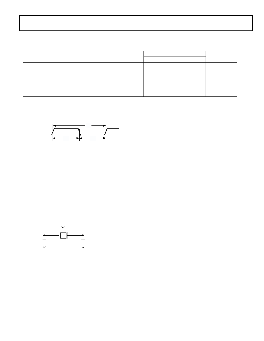
Note the definitions of various clock periods that are a function
of CLKIN and the appropriate ratio control (
Table 8
).
Figure 5
shows Core to CLKIN ratios of 6:1, 16:1 and 32:1 with
external oscillator or crystal. Note that more ratios are possible
and can be set through software using the power management
control register (PMCTL). For more information, see the
ADSP-2136x SHARC Processor Programming Reference.
Use the exact timing information given. Do not attempt to
derive parameters from the addition or subtraction of others.
While addition or subtraction would yield meaningful results
for an individual device, the values given in this data sheet
reflect statistical variations and worst cases. Consequently, it is
not meaningful to add parameters to derive longer times. See
Figure 38 on page 43
under Test Conditions for voltage refer-
ence levels.
Switching Characteristics specify how the processor changes its
signals. Circuitry external to the processor must be designed for
compatibility with these signal characteristics. Switching char-
acteristics describe what the processor will do in a given
circumstance. Use switching characteristics to ensure that any
timing requirement of a device connected to the processor (such
as memory) is satisfied.
Timing Requirements apply to signals that are controlled by cir-
cuitry external to the processor, such as the data input for a read
operation. Timing requirements guarantee that the processor
operates correctly with other devices.
Table 8. ADSP-21364 CLKOUT and CCLK Clock
Generation Operation
Timing
Requirements
Description
Calculation
CLKIN Input
Clock
1/t
CK
CCLK
Core Clock
1/t
CCLK
Table 9. Clock Periods
Timing
Requirements
Description
1
1
where:
SR = serial port-to-core clock ratio (wide range, determined by
SPORT CLKDIV)
SPIR = SPI-to-Core Clock Ratio (wide range, determined by
SPIBAUD register)
DAI_Px = Serial Port Clock
SPICLK = SPI Clock
t
CK
CLKIN Clock Period
t
CCLK
(Processor) Core Clock Period
t
PCLK
(Peripheral) Clock Period = 2 × t
CCLK
t
SCLK
Serial Port Clock Period = (t
PCLK
) × SR
t
SPICLK
SPI Clock Period = (t
PCLK
) × SPIR
Figure 5. Core Clock and System Clock Relationship to CLKIN
CLKIN
CCLK
(CORE CLOCK)
PLLILCLK
XTAL
XTAL
OSC
PLL
6:1, 16:1,
32:1
CLKOUT
CLK-CFG [1:0]
Rev. PrB
|
Page 18 of 52
|
September 2004
ADSP-21364
Preliminary Technical Data
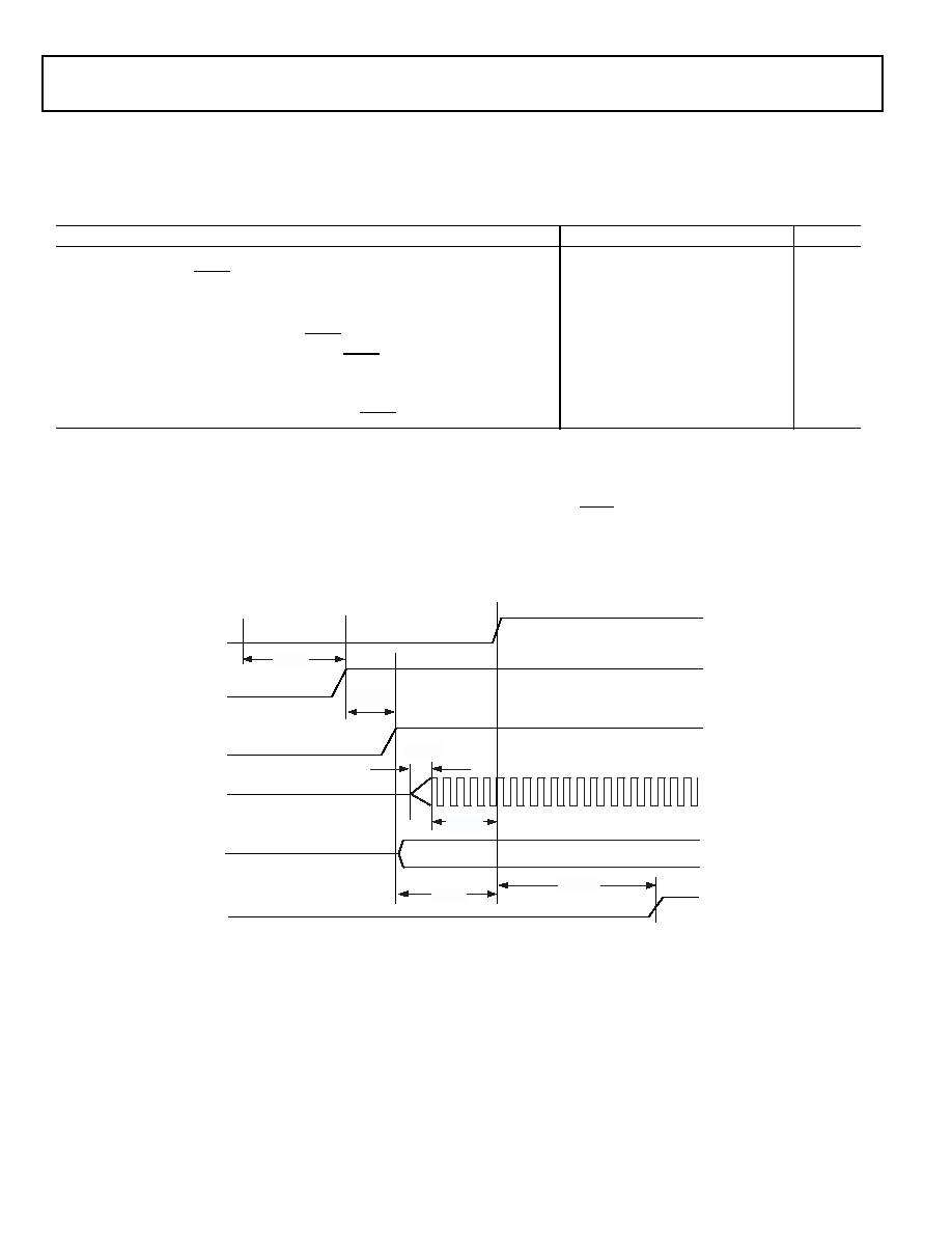
Power-Up Sequencing
The timing requirements for processor startup are given in
Table 10
.
Table 10. Power-Up Sequencing Timing Requirements (Processor Startup)
Parameter
Min
Max
Unit
Timing Requirements
t
RSTVDD
RESET Low Before V
DDINT
/V
DDEXT
on
0
ns
t
IVDDEVDD
V
DDINT
on Before V
DDEXT
50
200
ms
t
CLKVDD
1
CLKIN Valid After V
DDINT
/V
DDEXT
Valid
0
200
ms
t
CLKRST
CLKIN Valid Before RESET Deasserted
10
2
µs
t
PLLRST
PLL Control Setup Before RESET Deasserted
20
3
µs
Switching Characteristic
t
CORERST
Core Reset Deasserted After RESET Deasserted
4096t
CK
+ 2 t
CCLK
4, 5
1
Valid V
DDINT
/V
DDEXT
assumes that the supplies are fully ramped to their 1.2 and 3.3 volt rails. Voltage ramp rates can vary from microseconds to hundreds of milliseconds
depending on the design of the power supply subsystem.
2
Assumes a stable CLKIN signal, after meeting worst-case startup timing of crystal oscillators. Refer to your crystal oscillator manufacturer's datasheet for startup time.
Assume a 25 ms maximum oscillator startup time if using the XTAL pin and internal oscillator circuit in conjunction with an external crystal.
3
Based on CLKIN cycles
4
Applies after the power-up sequence is complete. Subsequent resets require a minimum of 4 CLKIN cycles for RESET to be held low in order to properly initialize and
propagate default states at all I/O pins.
5
The 4096 cycle count depends on t
SRST
specification in
Table 12
. If setup time is not met, 1 additional CLKIN cycle may be added to the core reset time, resulting in 4097
cycles maximum.
Figure 6. Power Up Sequencing
CLKIN
RESET
RSTOUT
VDDEXT
VDDINT
t
PLLRST
t
CLKRST
t
CLKVDD
t
IVDDEVDD
CLK_CFG1-0
t
CORERST
t
RSTVDD
ADSP-21364
Preliminary Technical Data
Rev. PrB
|
Page 19 of 52
|
September 2004
Clock Input
Clock Signals
The ADSP-21364 can use an external clock or a crystal. See
CLKIN pin description. The programmer can configure the
ADSP-21364 to use its internal clock generator by connecting
the necessary components to CLKIN and XTAL.
Figure 8
shows
the component connections used for a crystal operating in fun-
damental mode. Note that the clock rate is achieved using a
16.67 MHz crystal and a PLL multiplier ratio 16:1
(CCLK:CLKIN achieves a clock speed of 266 MHz). To achieve
the full core clock rate, programs need to configure the multi-
plier bits in the PMCTL register.
Table 11. Clock Input
Parameter
333 MHz
Unit
Min
Max
Timing Requirements
t
CK
CLKIN Period
18
1
1
Applies only for CLKCFG10 = 00 and default values for PLL control bits in PMCTL.
TBD
2
2
Applies only for CLKCFG10 = 01 and default values for PLL control bits in PMCTL.
ns
t
CKL
CLKIN Width Low
7.5
1
TBD
2
ns
t
CKH
CLKIN Width High
7.5
1
TBD
2
ns
t
CKRF
CLKIN Rise/Fall (0.4V2.0V)
TBD
ns
t
CCLK
3
3
Any changes to PLL control bits in the PMCTL register must meet core clock timing specification t
CCLK
.
CCLK Period
3.0
1
TBD
ns
Figure 7. Clock Input
CLKIN
t
CK
t
CKH
t
CKL
Figure 8. 333 MHz Operation (Fundamental Mode Crystal)
CLKIN
XTAL
C1
C2
X1
NOTE: C1 AND C2 ARE SPECIFIC TO CRYSTAL SPECIFIED FOR X1.
CONTACT CRYSTAL MANUFACTURER FOR DETAILS. CRYSTAL
SELECTION MUST COMPLY WITH CLKCFG1-0 = 10 OR = 01.
1M
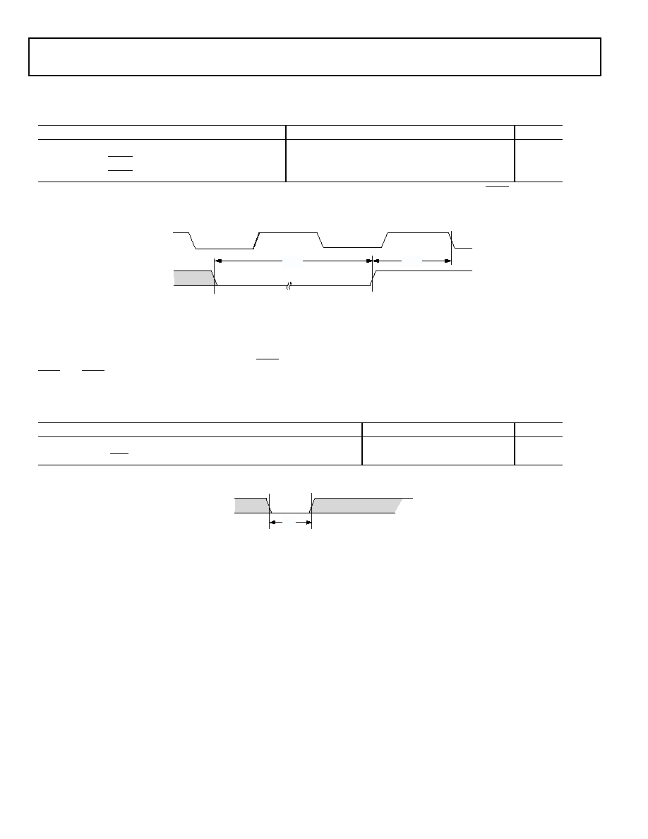
Rev. PrB
|
Page 20 of 52
|
September 2004
ADSP-21364
Preliminary Technical Data
Reset
Interrupts
The following timing specification applies to the FLAG0,
FLAG1, and FLAG2 pins when they are configured as IRQ0,
IRQ1, and IRQ2 interrupts. Also applies to DAI_P201 pins
when configured as interrupts
Table 12. Reset
Parameter
Min
Max
Unit
Timing Requirements
t
WRST
1
RESET Pulse Width Low
4t
CK
ns
t
SRST
RESET Setup Before CLKIN Low
8
ns
1
Applies after the power-up sequence is complete. At power-up, the processor's internal phase-locked loop requires no more than 100 µs while RESET is low, assuming
stable VDD and CLKIN (not including start-up time of external clock oscillator).
Figure 9. Reset
CLKIN
RESET
t
WRST
t
SRST
Table 13. Interrupts
Parameter
Min
Max
Unit
Timing Requirement
t
IPW
IRQx Pulse Width
2 × t
PCLK
+ 2
ns
Figure 10. Interrupts
DAI_P20-1
FLAG2-0
(IRQ2-0)
t
IPW
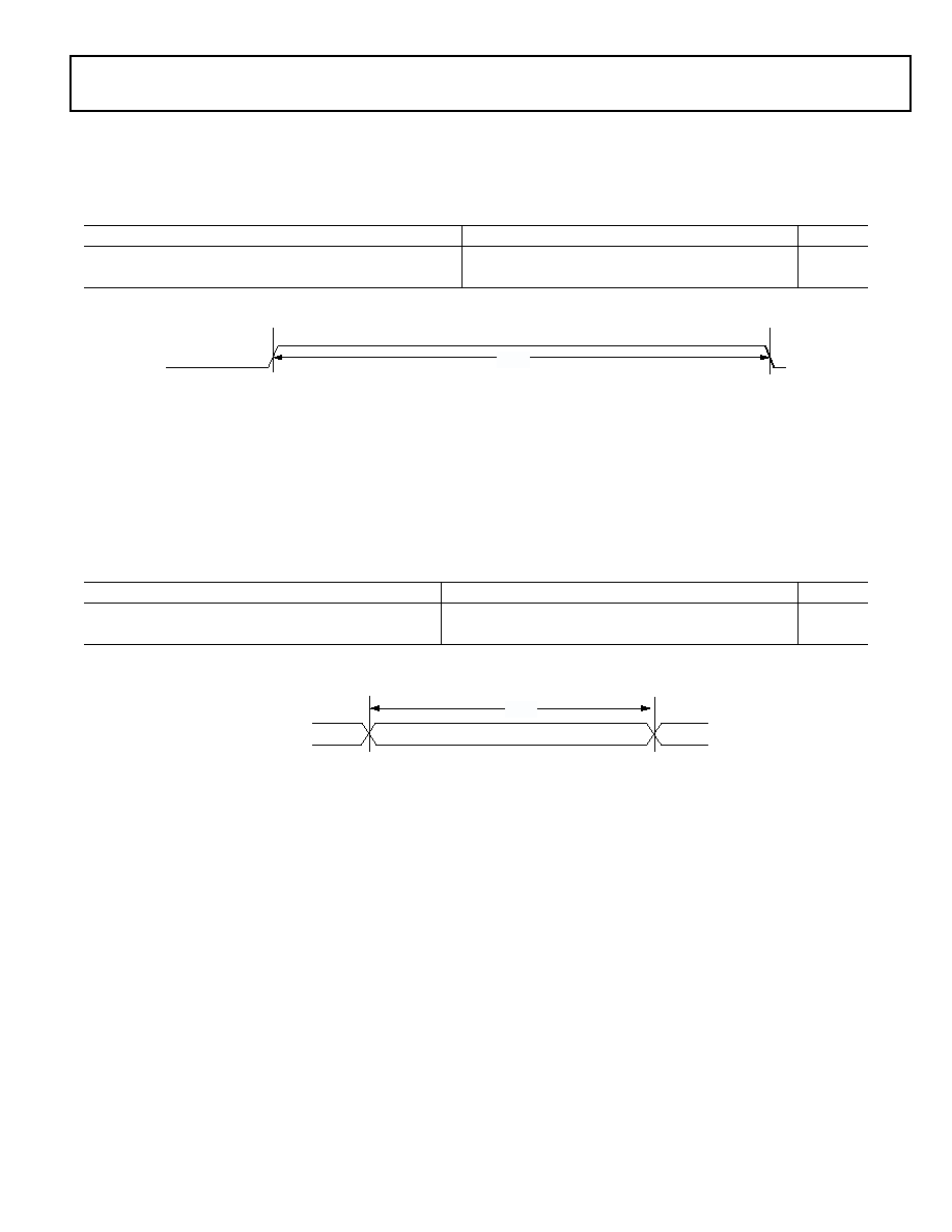
ADSP-21364
Preliminary Technical Data
Rev. PrB
|
Page 21 of 52
|
September 2004
Core Timer
The following timing specification applies to FLAG3 when it is
configured as the core timer (CTIMER).
Timer PWM_OUT Cycle Timing
The following timing specification applies to Timer0, Timer1,
and Timer2 in PWM_OUT (pulse width modulation) mode.
Timer signals are routed to the DAI_P201 pins through the
SRU. Therefore, the timing specifications provided below are
valid at the DAI_P201 pins.
Table 14. Core Timer
Parameter
Min
Max Unit
Switching Characteristic
t
WCTIM
CTIMER Pulse Width
4 × t
PCLK
1
ns
Figure 11. Core Timer
FLAG3
(CTIMER)
t
W CTIM
Table 15. Timer PWM_OUT Timing
Parameter
Min
Max Unit
Switching Characteristic
t
PWMO
Timer Pulse Width Output
2 t
PCLK
1
2(2
31
1) t
PCLK
ns
Figure 12. Timer PWM_OUT Timing
DAI_P20-1
(TIMER2-0)
t
PW MO
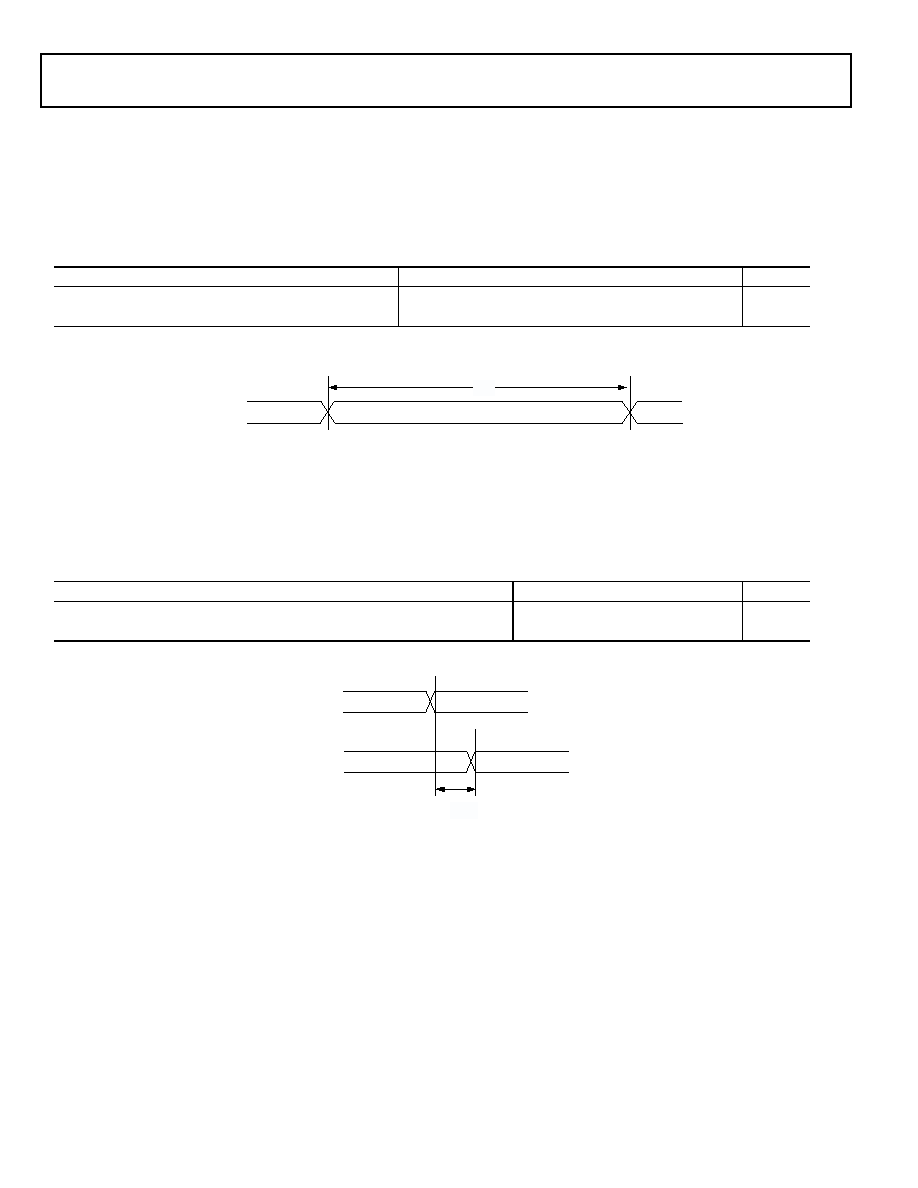
Rev. PrB
|
Page 22 of 52
|
September 2004
ADSP-21364
Preliminary Technical Data
Timer WDTH_CAP Timing
The following timing specification applies to Timer0, Timer1,
and Timer2 in WDTH_CAP (pulse width count and capture)
mode. Timer signals are routed to the DAI_P201 pins through
the SRU. Therefore, the timing specifications provided below
are valid at the DAI_P201 pins.
DAI Pin to Pin Direct Routing
For direct pin connections only (for example DAI_PB01_I to
DAI_PB02_O).
Table 16. Timer Width Capture Timing
Parameter
Min
Max Unit
Timing Requirement
t
PWI
Timer Pulse Width
2 t
PCLK
2(2
31
1) t
PCLK
ns
Figure 13. Timer Width Capture Timing
DAI_P20-1
(TIMER2-0)
t
PWI
Table 17. DAI Pin to Pin Routing
Parameter
Min
Max
Unit
Timing Requirement
t
DPIO
Delay DAI Pin Input Valid to DAI Output Valid
1.5
10
ns
Figure 14. DAI Pin to PIN Direct Routing
DAI_PN
t
DPIO
DAI_PM
ADSP-21364
Preliminary Technical Data
Rev. PrB
|
Page 23 of 52
|
September 2004
Precision Clock Generator (Direct Pin Routing)
This timing is only valid when the SRU is configured such that
the Precision Clock Generator (PCG) takes its inputs directly
from the DAI pins (via pin buffers) and sends its outputs
directly to the DAI pins. For the other cases, where the PCG's
inputs and outputs are not directly routed to/from DAI pins (via
pin buffers) there is not timing data available. All Timing
Parameters and Switching Characteristics apply to external DAI
pins (DAI_P07 DAI_P20).
Table 18. Precision Clock Generator (Direct Pin Routing)
Parameter
Min
Max
Unit
Timing Requirements
t
PCGIW
Input Clock Period
24
t
STRIG
PCG Trigger Setup Before Falling Edge of PCG Input Clock
2
ns
t
HTRIG
PCG Trigger Hold After Falling Edge of PCG Input Clock
2
ns
Switching Characteristics
t
DPCGIO
PCG Output Clock and Frame Sync Active Edge Delay After PCG
Input Clock
2.5
10
ns
t
DTRIG
PCG Output Clock and Frame Sync Delay After PCG Trigger
2.5 + 2.5 × t
PCGOW
10 + 2.5 × t
PCGOW
ns
t
PCGOW
Output Clock Period
48
Figure 15. Precision Clock Generator (Direct Pin Routing)
DAI_PN
PCG_TRIGX_I
t
STRIG
DAI_PM
PCG_EXTX_I
(CLKIN)
DAI_PY
PCG_CLKX_O
DAI_PZ
PCG_FSX_O
t
HTRIG
t
DPCGIO
t
DTRIG
t
PCGIW
t
PCGOW
Rev. PrB
|
Page 24 of 52
|
September 2004
ADSP-21364
Preliminary Technical Data
Flags
The timing specifications provided below apply to the FLAG30
and DAI_P201 pins, the parallel port and the serial peripheral
interface (SPI). See
Table 3, "Pin Descriptions," on page 11
for
more information on flag use.
Table 19. Flags
Parameter
Min
Max Unit
Timing Requirement
t
FIPW
FLAG30 IN Pulse Width
2 × t
PCLK
+ 3
ns
Switching Characteristic
t
FOPW
FLAG30 OUT Pulse Width
2 × t
PCLK
1
ns
Figure 16. Flags
DAI_P20-1
(FLAG3-0IN)
(AD15-0)
t
FIPW
DAI_P20-1
(FLAG3-0OUT)
(AD15-0)
t
FOPW
ADSP-21364
Preliminary Technical Data
Rev. PrB
|
Page 25 of 52
|
September 2004
Memory Read--Parallel Port
Use these specifications for asynchronous interfacing to memo-
ries (and memory-mapped peripherals) when the
ADSP-21364 is accessing external memory space.
Table 20. 8-Bit Memory Read Cycle
Parameter
Min
Max Unit
Timing Requirements
t
DRS
Address/Data 70 Setup Before RD High
3.3
ns
t
DRH
Address/Data 70 Hold After RD High
0
ns
t
DAD
Address 158 to Data Valid
D + t
PCLK
5
ns
Switching Characteristics
t
ALEW
ALE Pulse Width
2 × t
PCLK
2.0
ns
t
ADAS
1
Address/Data 150 Setup Before ALE Deasserted
t
PCLK
2.5
ns
t
RRH
Delay Between RD Rising Edge to Next Falling Edge.
H + t
PCLK
1
ns
t
ALERW
ALE Deasserted to Read Asserted
2 × t
PCLK
2
ns
t
RWALE
Read Deasserted to ALE Asserted
F + H + 0.5
ns
t
ADAH
1
Address/Data 150 Hold After ALE Deasserted
t
PCLK
0.8
t
ALEHZ
1
ALE Deasserted to Address/Data70 in High Z
t
PCLK
0.8
t
PCLK
ns
t
RW
RD Pulse Width
D 2
ns
t
RDDRV
RD Address Drive After Read High
F + H + t
PCLK
1
ns
t
ADRH
Address/Data 158 Hold After RD High
H
ns
D = (Data Cycle Duration = the value set by the PPDUR bits (51) in the PPCTL register) × t
PCLK
H = t
PCLK
(if a hold cycle is specified, else H = 0)
F = 7 x t
PCLK
(if FLASH_MODE is set else F = 0)
t
PCLK
= (Peripheral) Clock Period = 2 × t
CCLK
1
On reset, ALE is an active high cycle. However, it can be configured by software to be active low.
Figure 17. Read Cycle For 8-Bit Memory Timing
VALID ADDRESS
VALID
ADDRESS
AD15-8
t
ADAS
VALID ADDRESS
AD7-0
t
ALEW
ALE
RD
t
RW
WR
t
ADAH
t
ADRH
t
DRS
t
DRH
t
DAD
t
ALERW
t
RWALE
VALID
DATA
VALID
ADDRESS
t
RDDRV
t
ALEHZ
VALID ADDRESS
VALID ADDRESS
VALID
DATA
t
RRH
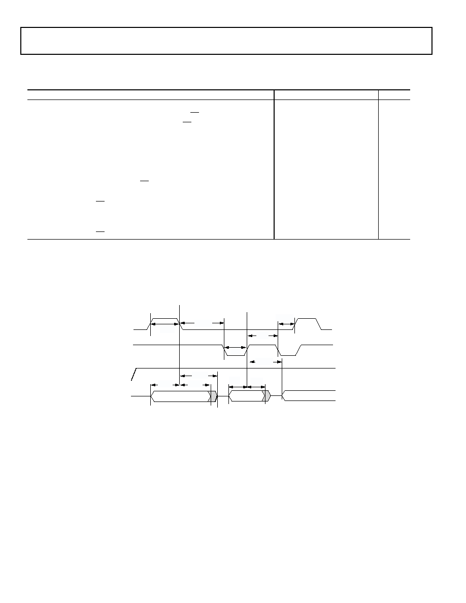
Rev. PrB
|
Page 26 of 52
|
September 2004
ADSP-21364
Preliminary Technical Data
Table 21. 16-bit Memory Read Cycle
Parameter
Min
Max Unit
Timing Requirements
t
DRS
Address/Data 150 Setup Before RD High
3.3
ns
t
DRH
Address/Data 150 Hold After RD High
0
ns
Switching Characteristics
ns
t
ALEW
ALE Pulse Width
2 × t
PCLK
2
ns
t
ADAS
1
Address/Data 150 Setup Before ALE Deasserted
t
PCLK
2.5
ns
t
ALERW
ALE Deasserted to Read Asserted
2 × t
PCLK
2
ns
t
RRH
Delay Between RD Rising Edge to Next Falling Edge.
H + t
PCLK
1
ns
t
RWALE
Read Deasserted to ALE Asserted
F + H + 0.5
ns
t
RDDRV
RD Address Drive After Read High
F + H + t
PCLK
1
ns
t
ADAH
1
Address/Data 150 Hold After ALE Deasserted
t
PCLK
0.8
ns
t
ALEHZ
1
ALE Deasserted to Address/Data150 in High Z
t
PCLK
0.8
ns
t
RW
RD Pulse Width
D 2
ns
D = (Data Cycle Duration = the value set by the PPDUR bits (51) in the PPCTL register) × t
PCLK
H = t
PCLK
(if a hold cycle is specified, else H = 0)
F = 7 x t
PCLK
(if FLASH_MODE is set else F = 0)
1
On reset, ALE is an active high cycle. However, it can be configured by software to be active low.
Figure 18. Read Cycle For 16-Bit Memory Timing
AD15-0
WR
t
DRS
t
DRH
t
RDDRV
t
ALEHZ
t
ADAH
t
ADAS
VALID ADDRESS
VALID DATA
VALID
ADDRESS
t
ALEW
t
RW
t
ALERW
t
RW ALE
t
RRH
ALE
RD
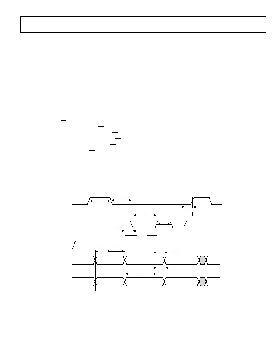
ADSP-21364
Preliminary Technical Data
Rev. PrB
|
Page 27 of 52
|
September 2004
Memory Write--Parallel Port
Use these specifications for asynchronous interfacing to memo-
ries (and memory-mapped peripherals) when the
ADSP-21364 is accessing external memory space.
Table 22. 8-bit Memory Write Cycle
Parameter
Min
Max Unit
Switching Characteristics:
t
ALEW
ALE Pulse Width
2 × t
PCLK
2
ns
t
ADAS
1
Address/Data 150 Setup Before ALE Deasserted
t
PCLK
2.5
ns
t
ALERW
ALE Deasserted to Read/Write Asserted
2 × t
PCLK
2
ns
t
RWALE
Write Deasserted to ALE Asserted
H + 0.5
ns
t
WRH
Delay Between WR Rising Edge to next WR Falling Edge
F + H + t
PCLK
2
ns
t
ADAH
1
Address/Data 150 Hold After ALE Deasserted
t
PCLK
0.5
ns
t
WW
WR Pulse Width
D F 2
ns
t
ADWL
Address/Data 158 to WR Low
t
PCLK
1.5
ns
t
ADWH
Address/Data 158 Hold After WR High
H
ns
t
DWS
Address/Data 70 Setup Before WR High
D F + t
PCLK
4
ns
t
DWH
Address/Data 70 Hold After WR High
H
ns
t
DAWH
Address/Data to WR High
D F + t
PCLK
4
ns
D = (Data Cycle Duration = the value set by the PPDUR bits (51) in the PPCTL register) × t
PCLK
H = t
PCLK
(if a hold cycle is specified, else H = 0)
F = 7 x t
PCLK
(if FLASH_MODE is set else F = 0)
1
On reset, ALE is an active high cycle. However, it can be configured by software to be active low.
Figure 19. Write Cycle For 8-Bit Memory Timing
AD15-8
VALID
ADDRESS
VALID ADDRESS
t
ADAS
AD7-0
ALE
RD
WR
t
ADAH
t
ADWH
t
ADWL
VALID DATA
t
DAWH
t
WRH
t
RWALE
VALID
ADDRESS
VALID DATA
t
ALEW
t
ALERW
t
WW
t
DWS
t
DWH
VALID ADDRESS
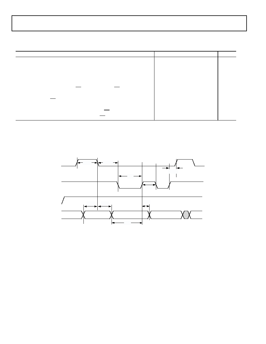
Rev. PrB
|
Page 28 of 52
|
September 2004
ADSP-21364
Preliminary Technical Data
Table 23. 16-bit Memory Write Cycle
Parameter
Min
Max Unit
Switching Characteristics
t
ALEW
ALE Pulse Width
2 × t
PCLK
2
ns
t
ADAS
1
Address/Data 150 Setup Before ALE Deasserted
t
PCLK
2.5
ns
t
ALERW
ALE Deasserted to Write Asserted
2 × t
PCLK
2
ns
t
RWALE
Write Deasserted to ALE Asserted
H + 0.5
ns
t
WRH
Delay Between WR Rising Edge to next WR Falling Edge
F + H + t
PCLK
2
ns
t
ADAH
1
Address/Data 150 Hold After ALE Deasserted
t
PCLK
0.5
ns
t
WW
WR Pulse Width
D F 2
ns
t
ALEHZ
1
ALE Deasserted to Address/Data150 in High Z
t
PCLK
1.5
ns
t
DWS
Address/Data 150 Setup Before WR High
D F + t
PCLK
4
ns
t
DWH
Address/Data 150 Hold After WR High
H
ns
D = (Data Cycle Duration = the value set by the PPDUR bits (51) in the PPCTL register) × t
PCLK
H = t
PCLK
(if a hold cycle is specified, else H = 0)
F = 7 x t
PCLK
(if FLASH_MODE is set else F = 0)
1
On reset, ALE is an active high cycle. However, it can be configured by software to be active low.
Figure 20. Write Cycle For 16-Bit Memory Timing
AD15-0
VALID
ADDRESS
VALID DATA
t
ADAS
ALE
RD
WR
t
ADAH
t
WRH
t
RWALE
t
ALEW
t
ALERW
t
WW
t
DWS
t
DWH
VALID DATA

ADSP-21364
Preliminary Technical Data
Rev. PrB
|
Page 29 of 52
|
September 2004
Serial Ports
To determine whether communication is possible between two
devices at clock speed n, the following specifications must be
confirmed: 1) frame sync delay and frame sync setup and hold,
2) data delay and data setup and hold, and 3) SCLK width.
Serial port signals (SCLK, FS, DxA,/DxB) are routed to the
DAI_P201 pins using the SRU. Therefore, the timing specifica-
tions provided below are valid at the DAI_P201 pins.
Table 24. Serial Ports--External Clock
Parameter
Min
Max Unit
Timing Requirements
t
SFSE
1
FS Setup Before SCLK
(Externally Generated FS in either Transmit or Receive Mode)
2.5
ns
t
HFSE
1
FS Hold After SCLK
(Externally Generated FS in either Transmit or Receive Mode)
2.5
ns
t
SDRE
1
Receive Data Setup Before Receive SCLK
2.5
ns
t
HDRE
1
Receive Data Hold After SCLK
2.5
ns
t
SCLKW
SCLK Width
24
ns
t
SCLK
SCLK Period
48
ns
Switching Characteristics
t
DFSE
2
FS Delay After SCLK
(Internally Generated FS in either Transmit or Receive Mode)
7
ns
t
HOFSE
2
FS Hold After SCLK
(Internally Generated FS in either Transmit or Receive Mode)
2
ns
t
DDTE
2
Transmit Data Delay After Transmit SCLK
7
ns
t
HDTE
2
Transmit Data Hold After Transmit SCLK
2
ns
1
Referenced to sample edge.
2
Referenced to drive edge.
Table 25. Serial Ports--Internal Clock
Parameter
Min
Max Unit
Timing Requirements
t
SFSI
1
FS Setup Before SCLK
(Externally Generated FS in either Transmit or Receive Mode)
7
ns
t
HFSI
1
FS Hold After SCLK
(Externally Generated FS in either Transmit or Receive Mode)
2.5
ns
t
SDRI
1
Receive Data Setup Before SCLK
7
ns
t
HDRI
1
Receive Data Hold After SCLK
2.5
ns
Switching Characteristics
t
DFSI
2
FS Delay After SCLK (Internally Generated FS in Transmit Mode)
3
ns
t
HOFSI
2
FS Hold After SCLK (Internally Generated FS in Transmit Mode)
1.0
ns
t
DFSI
2
FS Delay After SCLK (Internally Generated FS in Receive or Mode)
3
ns
t
HOFSI
2
FS Hold After SCLK (Internally Generated FS in Receive Mode)
1.0
ns
t
DDTI
2
Transmit Data Delay After SCLK
3
ns
t
HDTI
2
Transmit Data Hold After SCLK
1.0
ns
t
SCLKIW
Transmit or Receive SCLK Width
0.5t
SCLK
2
0.5t
SCLK
+ 2
ns
1
Referenced to the sample edge.
2
Referenced to drive edge.
Rev. PrB
|
Page 30 of 52
|
September 2004
ADSP-21364
Preliminary Technical Data
Table 26. Serial Ports--Enable and Three-State
Parameter
Min
Max Unit
Switching Characteristics
t
DDTEN
1
Data Enable from External Transmit SCLK
2
ns
t
DDTTE
1
Data Disable from External Transmit SCLK
7
ns
t
DDTIN
1
Data Enable from Internal Transmit SCLK
1
ns
1
Referenced to drive edge.
Table 27. Serial Ports--External Late Frame Sync
Parameter
Min
Max Unit
Switching Characteristics
t
DDTLFSE
1
Data Delay from Late External Transmit FS or External Receive FS
with MCE = 1, MFD = 0
7
ns
t
DDTENFS
1
Data Enable for MCE = 1, MFD = 0
1
0.5
ns
1
The t
DDTLFSE
and t
DDTENFS
parameters apply to Left-justified Sample Pair as well as DSP serial mode, and MCE = 1, MFD = 0.
Figure 21. External Late Frame Sync
1
1
This figure reflects changes made to support Left-justified Sample Pair mode.
DRIVE
SAMPLE
DRIVE
DAI_P20-1
(SCLK)
DAI_P20-1
(FS)
DAI_P20-1
(DATA CHANNEL A/B)
DRIVE
SAMPLE
DRIVE
LATE EXTERNAL TRANSMIT FS
EXTERNAL RECEIVE FS WITH MCE = 1, MFD = 0
1ST BIT
2ND BIT
DAI_P20-1
(SCLK)
DAI_P20-1
(FS)
1ST BIT
2ND BIT
t
HFSE/I
t
SFSE/I
t
DDTE/I
t
DDTENFS
t
DDTLFSE
t
HDTE/I
t
SFSE/I
t
DDTE/I
t
DDTENFS
t
DDTLFSE
t
HDTE/I
DAI_P20-1
(DATA CHANNEL A/B)
NOTE
SERIAL PORT SIGNALS (SCLK, FS,
DATA CHANNEL A/B
) ARE ROUTED TO THE DAI_P20-1 PINS
USING THE SRU. THE TIMING SPECIFICATIONS PROVIDED HERE ARE VALID AT THE DAI_P20-1 PINS.
t
HFSE/I
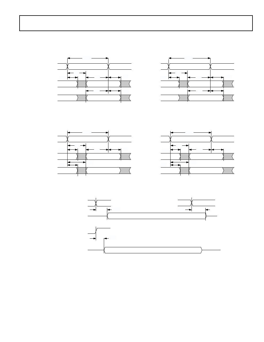
ADSP-21364
Preliminary Technical Data
Rev. PrB
|
Page 31 of 52
|
September 2004
Figure 22. Serial Ports
DRIVE EDGE
DAI_P20-1
SCLK (INT)
DRIVE EDGE
DRIVE EDGE
SCLK
DAI_P20-1
SCLK (EXT)
t
DDTTE
t
DDTEN
t
DDTIN
DAI_P20-1
(DATA CHANNEL A/B)
DAI_P20-1
(DATA CHANNEL A/B)
DAI_P20-1
(SCLK)
DAI_P20-1
(FS)
DRIVE EDGE
SAMPLE EDGE
DATA RECEIVE-- INTERNAL CLOCK
DATA RECEIVE-- EXTERNAL CLOCK
DRIVE EDGE
SAMPLE EDGE
NOTE: EITHER THE RISING EDGE OR FALLING EDGE OF SCLK (EXTERNAL), SCLK (INTERNAL) CAN BE USED AS THE ACTIVE SAMPLING EDGE.
t
SDRI
t
HDRI
t
SFSI
t
HFSI
t
DFSI
t
HOFSI
t
SCLKIW
t
SDRE
t
HDRE
t
SFSE
t
HFSE
t
DFSE
t
SCLKW
t
HOFSE
DAI_P20-1
(DATA CHANNEL A/B)
t
DDTI
DRIVE EDGE
SAMPLE EDGE
DATA TRANSMIT -- INTERNAL CLOCK
t
SFSI
t
HFSI
t
DFSI
t
HOFSI
t
SCLKIW
t
HDTI
NOTE: EITHER THE RISING EDGE OR FALLING EDGE OF SCLK (EXTERNAL), SCLK (INTERNAL) CAN BE USED AS THE ACTIVE SAMPLING EDGE.
t
DDTE
DRIVE EDGE
SAMPLE EDGE
DATA TRANSMIT -- EXTERNAL CLOCK
t
SFSE
t
HFSE
t
DFSE
t
HOFSE
t
SCLKW
t
HDTE
DAI_P20-1
(SCLK)
DAI_P20-1
(FS)
DAI_P20-1
(DATA CHANNEL A/B)
DAI_P20-1
(SCLK)
DAI_P20-1
(FS)
DAI_P20-1
(DATA CHANNEL A/B)
DAI_P20-1
(SCLK)
DAI_P20-1
(FS)
DAI_P20-1
(DATA CHANNEL A/B)
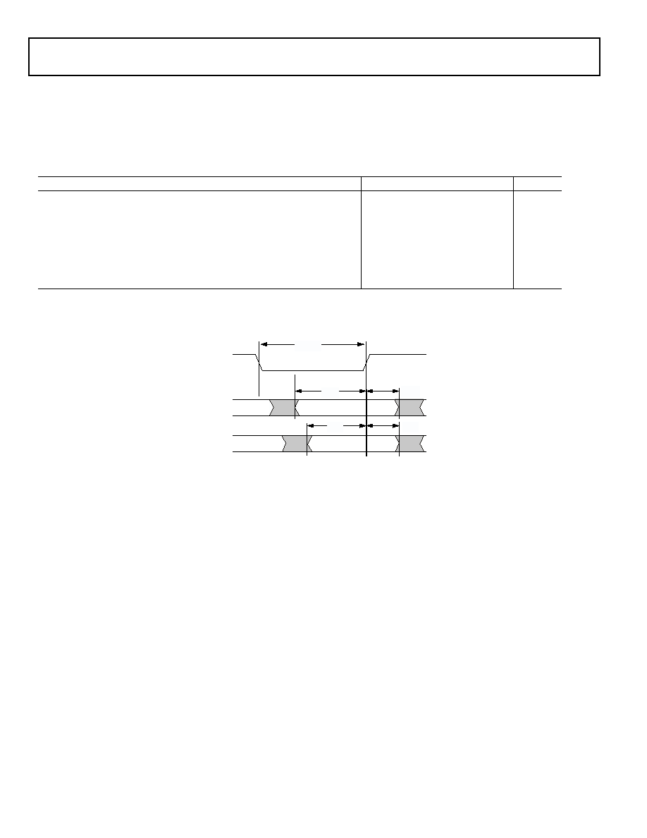
Rev. PrB
|
Page 32 of 52
|
September 2004
ADSP-21364
Preliminary Technical Data
Input Data Port (IDP)
The timing requirements for the IDP are given in
Table 28
.IDP
Signals (SCLK, FS, SDATA) are routed to the DAI_P201 pins
using the SRU. Therefore, the timing specifications provided
below are valid at the DAI_P201 pins.
Table 28. IDP
Parameter
Min
Max Unit
Timing Requirements
t
SIFS
1
FS Setup Before SCLK Rising Edge
2.5
ns
t
SIHFS
1
FS Hold After SCLK Rising Edge
2.5
ns
t
SISD
1
SData Setup Before SCLK Rising Edge
2.5
ns
t
SIHD
1
SData Hold After SCLK Rising Edge
2.5
ns
t
IDPCLKW
Clock Width
9
ns
t
IDPCLK
Clock Period
24
ns
1
DATA, SCLK, FS can come from any of the DAI pins. SCLK and FS can also come via PCG or SPORTs. PCG's input can be either CLKIN or any of the DAI pins.
Figure 23. IDP Master Timing
DAI_P20-1
(SCLK)
DAI_P20-1
(FS)
SAMPLE EDGE
t
SISD
t
SIHD
t
SISFS
t
SIHFS
t
SISCLKW
DAI_P20-1
(SDATA)
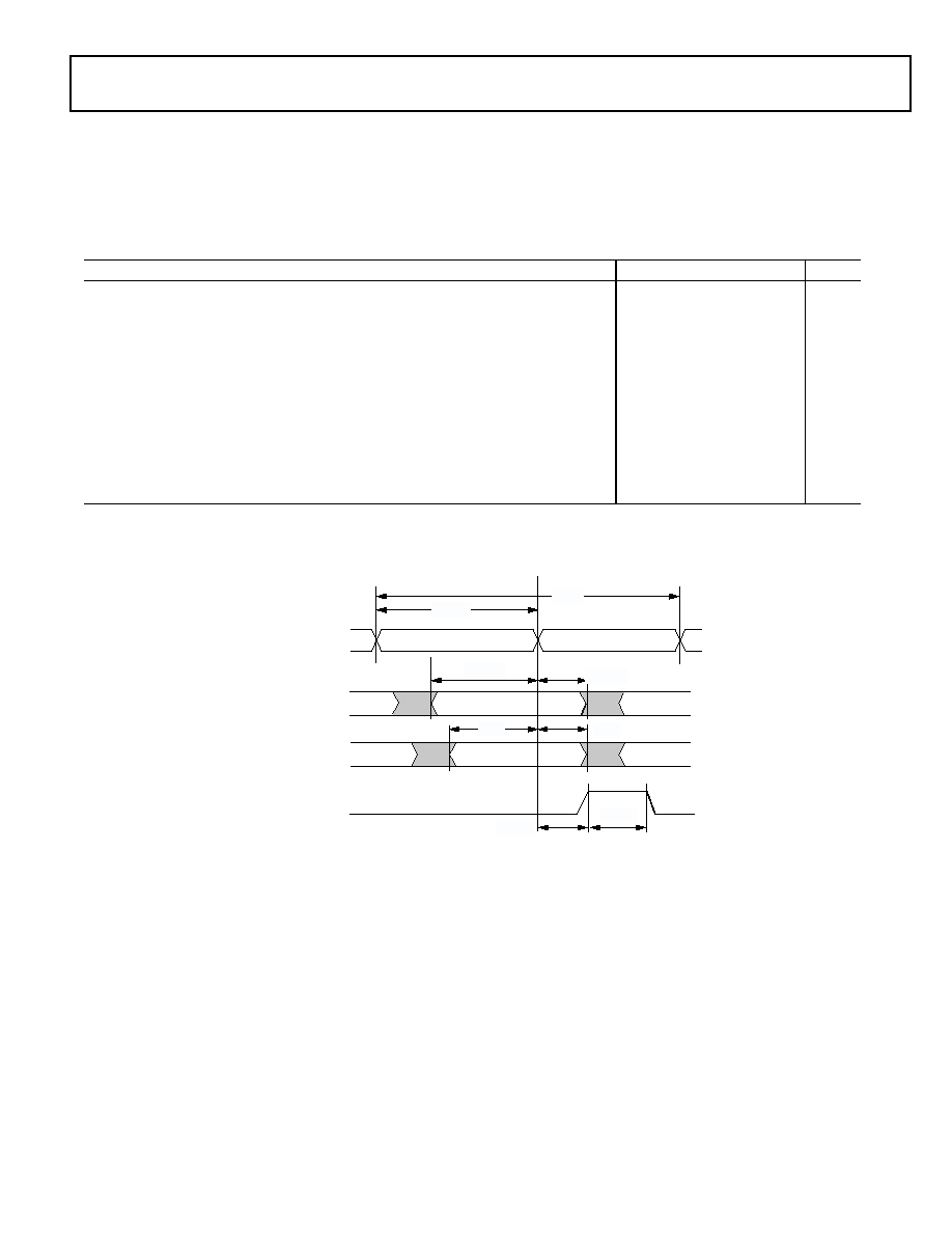
ADSP-21364
Preliminary Technical Data
Rev. PrB
|
Page 33 of 52
|
September 2004
Parallel Data Acquisition Port (PDAP)
The timing requirements for the PDAP are provided in
Table 29
. PDAP is the parallel mode operation of channel 0 of
the IDP. For details on the operation of the IDP, see the IDP
chapter of the ADSP-2136x SHARC Processor Hardware Refer-
ence. Note that the most significant 16 bits of external PDAP
data can be provided through either the parallel port AD150 or
the DAI_P205 pins. The remaining 4 bits can only be sourced
through DAI_P41. The timing below is valid at the
DAI_P201 pins or at the AD150 pins.
Table 29. Parallel Data Acquisition Port (PDAP)
Parameter
Min
Max
Unit
Timing Requirements
t
SPCLKEN
1
PDAP_CLKEN Setup Before PDAP_CLK Sample Edge
2.5
ns
t
HPCLKEN
1
PDAP_CLKEN Hold After PDAP_CLK Sample Edge
2.5
ns
t
PDSD
1
PDAP_DAT Setup Before SCLK PDAP_CLK Sample Edge
2.5
ns
t
PDHD
1
PDAP_DAT Hold After SCLK PDAP_CLK Sample Edge
2.5
ns
t
PDCLKW
Clock Width
7
ns
t
PDCLK
Clock Period
24
ns
Switching Characteristics
t
PDHLDD
Delay of PDAP Strobe After Last PDAP_CLK Capture Edge for a Word
2 × t
CCLK
ns
t
PDSTRB
PDAP Strobe Pulse Width
1 × t
CCLK
1
ns
1
Source pins of DATA are ADDR70, DATA70, or DAI pins. Source pins for SCLK and FS are: 1) DAI pins, 2) CLKIN through PCG, or 3) DAI pins through PCG.
Figure 24. PDAP Timing
DAI_P20-1
(PDAP_CLK)
SAMPLE EDGE
t
PDSD
t
PDHD
t
SPCLKEN
t
HPCLKEN
t
PDCLKW
DATA
DAI_P20-1
(PDAP_CLKEN)
t
PDSTRB
t
PDHLDD
DAI_P20-1
(PDAP_STROBE)
t
PDCLK
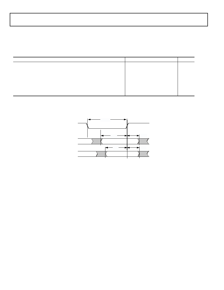
Rev. PrB
|
Page 34 of 52
|
September 2004
ADSP-21364
Preliminary Technical Data
Sample Rate Converter--Serial Input Port
The SRC input signals (SCLK, FS, and SDATA) are routed from
the DAI_P201 pins using the SRU. Therefore, the timing spec-
ifications provided in
Table 30
are valid at the DAI_P201 pins.
Table 30. SRC, Serial Input Port
Parameter
Min
Max Unit
Timing Requirements
t
SIFS
1
FS Setup Before SCLK Rising Edge
4
ns
t
SIHFS
1
FS Hold After SCLK Rising Edge
5.5
ns
t
SISD
1
SData Setup Before SCLK Rising Edge
4
ns
t
SIHD
1
SData Hold After SCLK Rising Edge
5.5
ns
t
IDPCLKW
Clock Width
9
ns
t
IDPCLK
Clock Period
20
ns
1
DATA, SCLK, FS can come from any of the DAI pins. SCLK and FS can also come via PCG or SPORTs. PCG's input can be either CLKIN or any of the DAI pins.
Figure 25. SRC Serial Input Port Timing
DAI_P20-1
(SCLK)
DAI_P20-1
(FS)
SAMPLE EDGE
t
SISD
t
SIHD
t
SISFS
t
SIHFS
t
IDPCLKW
DAI_P20-1
(SDATA)
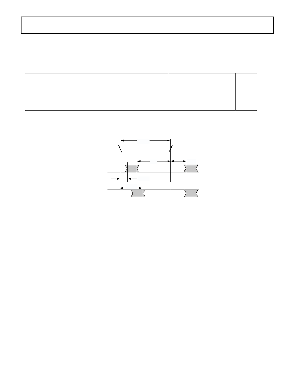
ADSP-21364
Preliminary Technical Data
Rev. PrB
|
Page 35 of 52
|
September 2004
Sample Rate Converter--Serial Output Port
For the serial output port, the frame-sync is an input and it
should meet setup and hold times with regard to SCLK on the
output port. The serial data output, SDATA, has a hold time
and delay specification with regard to SCLK. Note that SCLK
rising edge is the sampling edge and the falling edge is the drive
edge.
Table 31. SRC, Serial Output Port
Parameter
Min
Max Unit
Timing Requirements
t
SIFS
1
FS Setup Before SCLK Rising Edge
4
ns
t
SIHFS
1
FS Hold Before SCLK Rising Edge
5.5
ns
t
SRCTDD
1
Transmit Data Delay After SCLK Falling Edge
7
ns
t
SRCTDH
1
Transmit Data Hold After SCLK Falling Edge
2
ns
1
DATA, SCLK, FS can come from any of the DAI pins. SCLK and FS can also come via PCG or SPORTs. PCG's input can be either CLKIN or any of the DAI pins.
Figure 26. SRC Serial Output Port Timing
DAI_P20-1
(SCLK)
DAI_P20-1
(FS)
SAMPLE EDGE
t
SIFS
t
SIHFS
t
SISCLKW
DAI_P20-1
(SDATA)
t
SRCTDD
t
SR CTDH
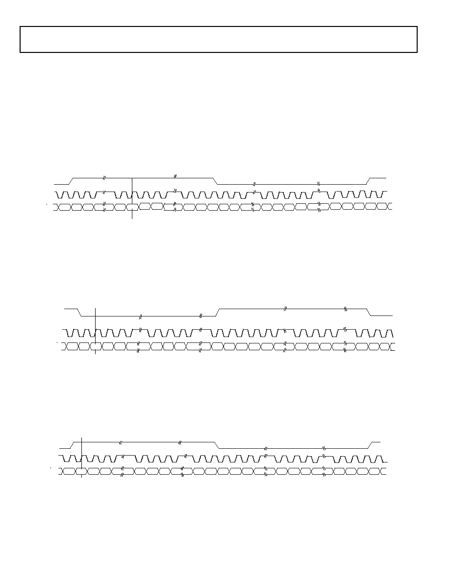
Rev. PrB
|
Page 36 of 52
|
September 2004
ADSP-21364
Preliminary Technical Data
SPDIF Transmitter
Serial data input to the SPDIF transmitter can be formatted as
left justified, I
2
S or right justified with word widths of 16, 18, 20,
or 24 bits. The following sections provide timing for the
transmitter.
SPDIF Transmitter--Serial Input Waveforms
Figure 27
shows the right-justified mode. LRCLK is HI for the
left channel and LO for the right channel. Data is valid on the
rising edge of SCLK. The MSB is delayed 12-bit clock periods
(in 20-bit output mode) or 16-bit clock periods (in 16-bit output
mode) from an LRCLK transition, so that when there are 64
SCLK periods per LRCLK period, the LSB of the data will be
right-justified to the next LRCLK transition.
Figure 28
shows the default I2S-justified mode. LRCLK is LO
for the left channel and HI for the right channel. Data is valid on
the rising edge of SCLK. The MSB is left-justified to an LRCLK
transition but with a single SCLK period delay.
Figure 29
shows the left-justified mode. LRCLK is HI for the left
channel and LO for the right channel. Data is valid on the rising
edge of SCLK. The MSB is left-justified to an LRCLK transition
with no MSB delay.
Figure 27. Right-Justified Mode
LRCLK
SCLK
SDATA
LEFT CHANNEL
RIGHT CHANNEL
MSB-1
MSB-2
LSB+2 LSB+1
LSB
MSB
MSB-1
MSB-2
LSB+2
LSB+1
LSB
LSB
MSB
Figure 28. I
2
S-Justified Mode
MSB-1
MSB-2
LSB+2 LSB+1
LSB
LRCLK
SCLK
SDATA
LEFT CHANNEL
RIGHT CHANNEL
MSB
MSB-1
MSB-2
LSB+2
LSB+1
LSB
MSB
MSB
Figure 29. Left-Justified Mode
LRCLK
SCLK
SDATA
LEFT CHANNEL
RIGHT CHANNEL
MSB-1
MSB-2
LSB+2
LSB+1
LSB
MSB
MSB-1
MSB-2
LSB+2
LSB+1
LSB
MSB
MSB+1
MSB
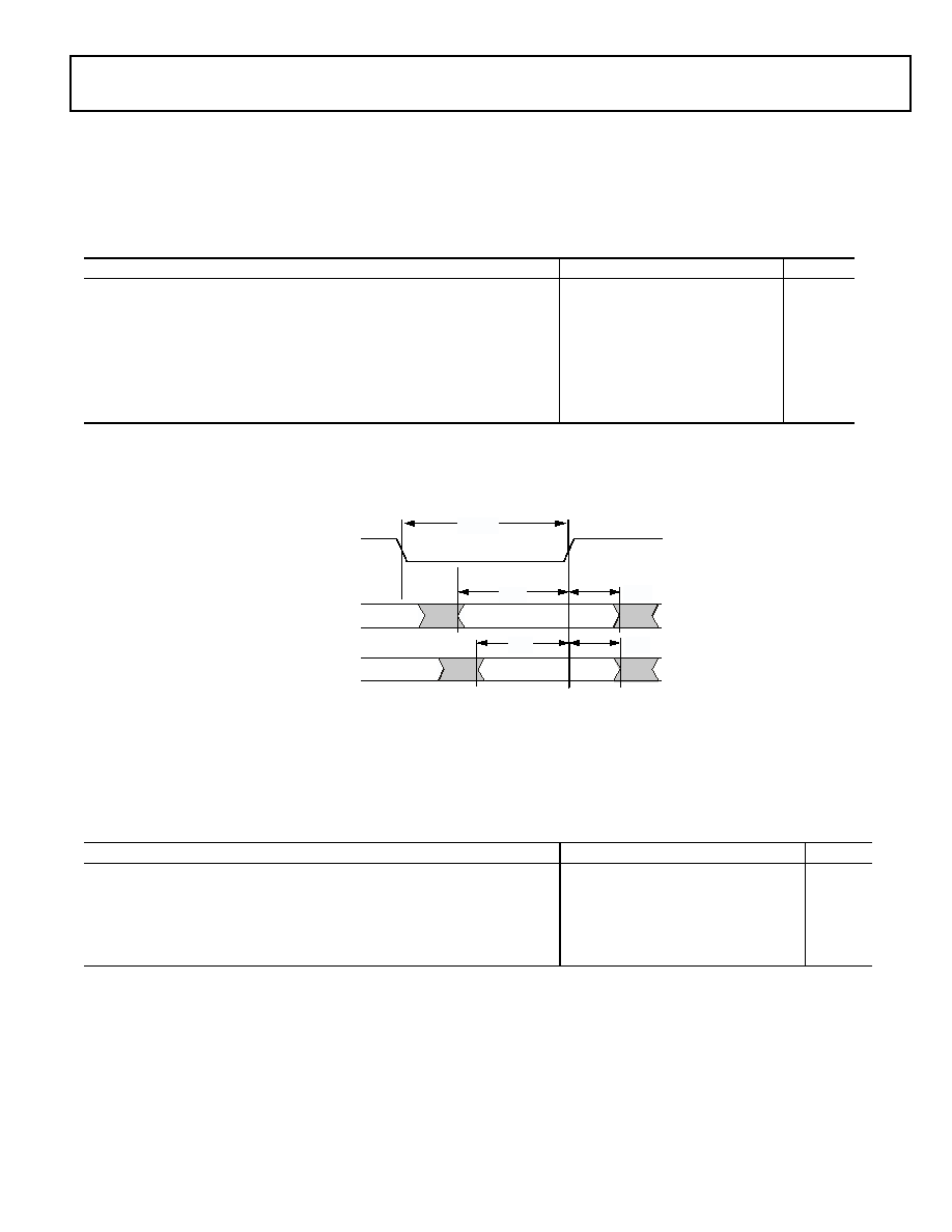
ADSP-21364
Preliminary Technical Data
Rev. PrB
|
Page 37 of 52
|
September 2004
SPDIF Transmitter Input Data Timing
The timing requirements for the Input port are given in
Table 32
. Input Signals (SCLK, FS, SDATA) are routed to the
DAI_P201 pins using the SRU. Therefore, the timing specifica-
tions provided below are valid at the DAI_P201 pins.
Over Sampling Clock (TXCLK) Switching Characteristics
SPDIF Transmitter has an over sampling clock. This TXCLK
input is divided down to generate the Biphase Clock.
Table 32. SPDIF Transmitter Input Data Timing
Parameter
Min
Max Unit
Timing Requirements
t
SIFS
1
FS Setup Before SCLK Rising Edge
4
ns
t
SIHFS
1
FS Hold After SCLK Rising Edge
5.5
ns
t
SISD
1
SData Setup Before SCLK Rising Edge
4
ns
t
SIHD
1
SData Hold After SCLK Rising Edge
5.5
ns
t
SISCLKW
Clock Width
9
ns
t
SISCLK
Clock Period
20
ns
1
DATA, SCLK, FS can come from any of the DAI pins. SCLK and FS can also come via PCG or SPORTs. PCG's input can be either CLKIN or any of the DAI pins.
Figure 30. SPDIF Transmitter Input Timing
DAI_P20-1
(SCLK)
DAI_P20-1
(FS)
SAMPLE EDGE
t
SISD
t
SIH D
t
SISFS
t
SIHFS
t
SISCLKW
DAI_P20-1
(SDATA)
Table 33. Over Sampling Clock (TXCLK) Switching Characteristics
Parameter
Min
Max
Unit
TXCLK Frequency for TXCLK = 768 × FS
147.5
MHz
TXCLK Frequency for TXCLK = 512 × FS
98.4
MHz
TXCLK Frequency for TXCLK = 384 × FS
73.8
MHz
TXCLK Frequency for TXCLK = 256 × FS
49.2
MHz
Frame Rate
192.0
MHz
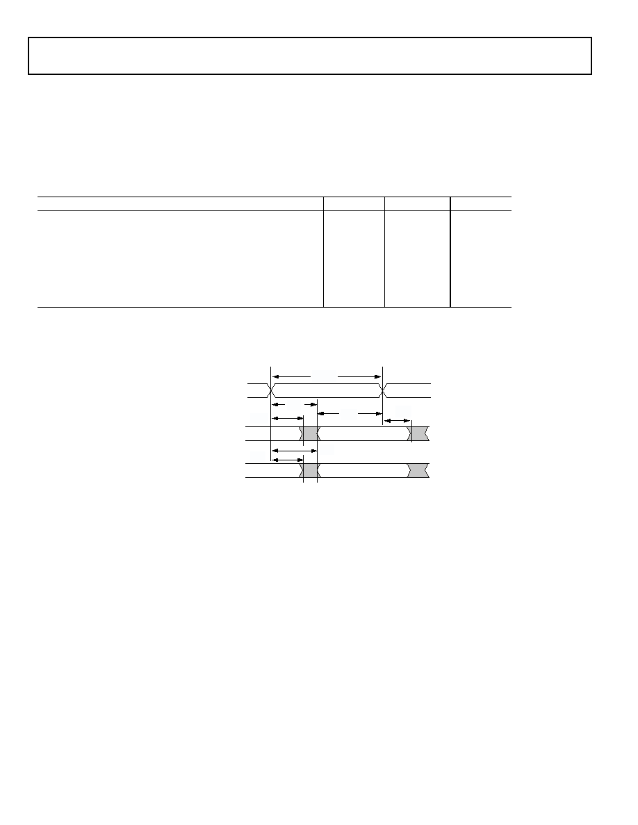
Rev. PrB
|
Page 38 of 52
|
September 2004
ADSP-21364
Preliminary Technical Data
SPDIF Receiver
The following sections describe timing as it relates to the SPDIF
receiver.
Internal Digital PLL Mode
In internal Digital Phase-locked Loop mode the internal PLL
(Digital PLL) generates the 512
×
Fs clock.
Table 34. SPDIF Receiver Internal Digital PLL Mode Timing
Parameter
Min
Max
Unit
Switching Characteristics
t
DFSI
LRCLK Delay After SCLK
5
ns
t
HOFSI
LRCLK Hold After SCLK
2
ns
t
DDTI
Transmit Data Delay After SCLK
5
ns
t
HDTI
Transmit Data Hold After SCLK
2
ns
t
SCLKIW
1
Transmit SCLK Width
40
ns
t
CCLK
Core Clock Period
5
ns
1
SCLK frequency is 64 x FS where FS = the frequency of LRCLK.
Figure 31. SPDIF Receiver Internal Digital PLL Mode Timing
DRIVE EDGE
SAMPLE EDGE
DAI_P20-1
(SCLK)
DAI_P20-1
(FS)
DAI_P20-1
(DATA CHANNEL A/B)
t
SCLKIW
t
DFSI
t
DDTI
t
HOFSI
t
HDTI
t
SFSI
t
HFSI
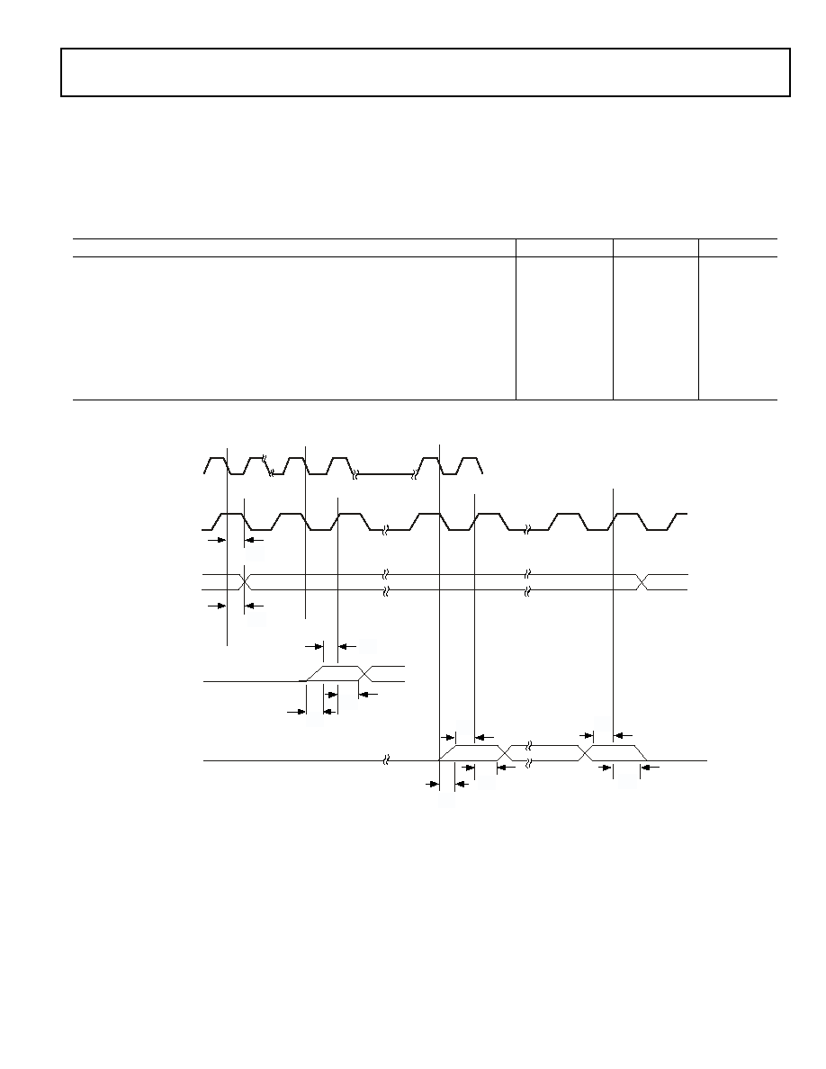
ADSP-21364
Preliminary Technical Data
Rev. PrB
|
Page 39 of 52
|
September 2004
External PLL Mode
In External PLL Mode internal Digital PLL is disabled and the
receiver runs on the PLL that is connected to the processor
externally. This external PLL generates the 512 x Fs clock
(MCLK) from the reference clock (LRCLK) and gives it to
SPDIF receiver.
Table 35. SPDIF Receiver External PLL Mode Timing
Parameter
Min
Max
Unit
Timing Requirements
t
MCP
MCLK Period
10
ns
FMCLK
MCLK Frequency (1/t
MCP
)
100
MHz
t
BDM
SCLK Propagation Delay from MCLK to the Falling Edge
30
ns
t
LDM
LRCLK Propagation Delay From MCLK
30
ns
t
DDP
Data Propagation Delay From MCLK
30
ns
t
DDS
Data Output Setup To SCLK
1/2 SCLK Period
ns
t
DDH
Data Output Hold From SCLK
1/2 SCLK Period
ns
Figure 32. SPDIF Receiver External PLL Mode Timing
t
LDM
t
BDM
t
DDS
MSB
t
DDH
MCLK INPUT
(NOT TO SCALE)
BCLK OUTPUT
LRCLK
OUTPUT
SDATA OUTPUT
I2S-JUSTIFIED
MODE
t
DDP
t
DDS
t
DDH
t
DDP
MSB
LSB
t
DDH
t
DDS
SDATA OUTPUT
RIGHT-JUSTIFIED
MODE
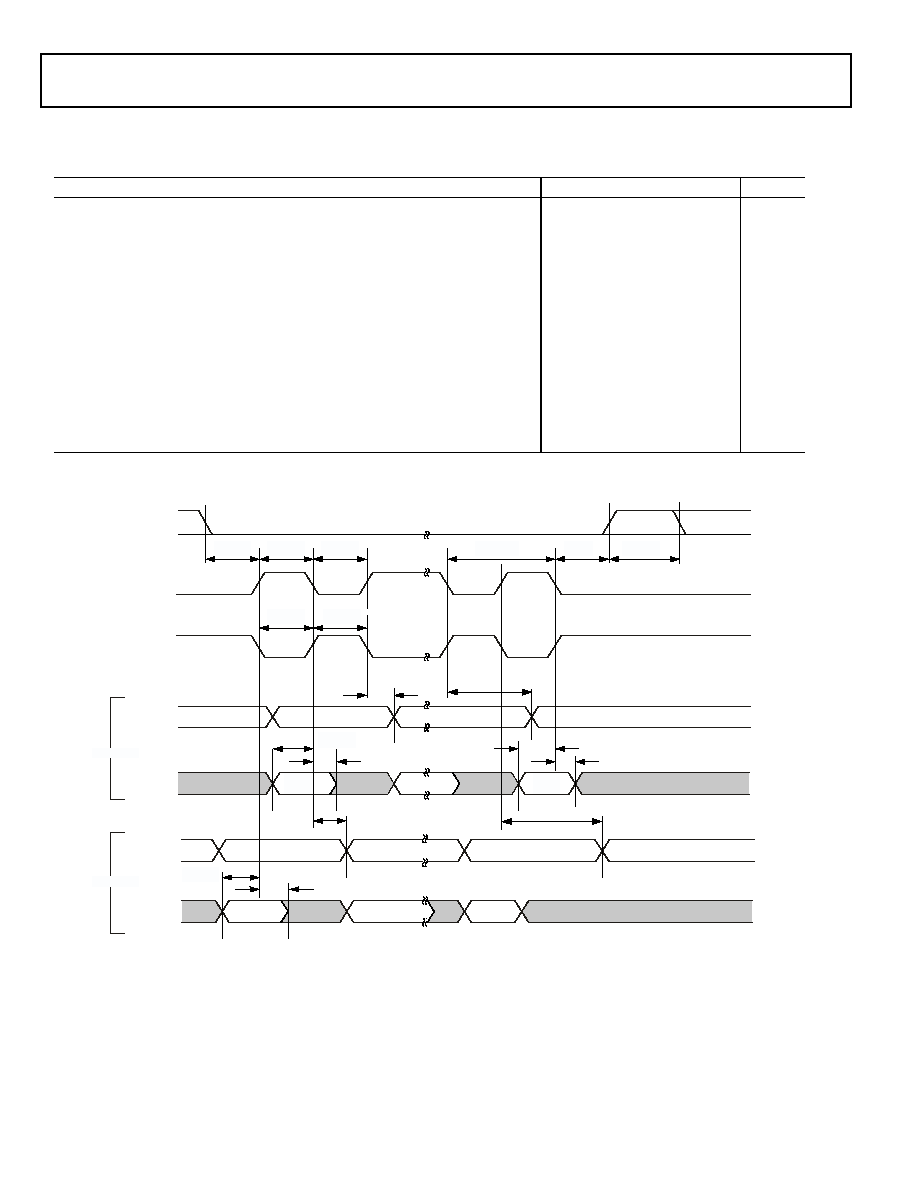
Rev. PrB
|
Page 40 of 52
|
September 2004
ADSP-21364
Preliminary Technical Data
SPI Interface--Master
Table 36. SPI Interface Protocol -- Master Switching and Timing Specifications
Parameter
Min
Max Unit
Timing Requirements
t
SSPIDM
Data Input Valid to SPICLK Edge (Data Input Set-up Time)
8
ns
t
HSPIDM
SPICLK Last Sampling Edge to Data Input Not Valid
2
ns
Switching Characteristics
t
SPICLKM
Serial Clock Cycle
8 × t
PCLK
ns
t
SPICHM
Serial Clock High Period
4 × t
PCLK
ns
t
SPICLM
Serial Clock Low Period
4 × t
PCLK
2
ns
t
DDSPIDM
SPICLK Edge to Data Out Valid (Data Out Delay Time)
0
t
HDSPIDM
SPICLK Edge to Data Out Not Valid (Data Out Hold Time)
2
ns
t
SDSCIM
FLAG30IN (SPI Device Select) Low to First SPICLK Edge
4 × t
PCLK
2
ns
t
HDSM
Last SPICLK edge to FLAG30IN High
4 × t
PCLK
1
ns
t
SPITDM
Sequential Transfer Delay
4 × t
PCLK
1
ns
Figure 33. SPI Master Timing
LSB
VALID
MSB
VALID
t
S S P ID M
t
H S P I D M
t
HDSPIDM
LSB
MSB
t
H S S P I D M
t
D D S P I D M
MOSI
(OUTPUT)
MISO
(INPUT)
FLAG3-0
(OUTPUT)
SPICLK
(CP = 0)
(OUTPUT)
SPICLK
(CP = 1)
(OUTPUT)
t
S P I C H M
t
S P I C L M
t
S P I C L M
t
S P I C L K M
t
S P I C H M
t
H D S M
t
S P I TD M
t
H D S P I D M
LSB
VALID
LSB
MSB
MSB
VALID
t
H S P I D M
t
D D S P I D M
MOSI
(OUTPUT)
MISO
(INPUT)
t
S S P ID M
CPHASE=1
CPHASE=0
t
S D S C I M
t
S S P I D M
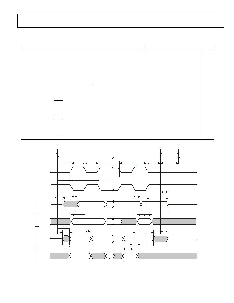
ADSP-21364
Preliminary Technical Data
Rev. PrB
|
Page 41 of 52
|
September 2004
SPI Interface--Slave
Table 37. SPI Interface Protocol --Slave Switching and Timing Specifications
Parameter
Min
Max Unit
Timing Requirements
t
SPICLKS
Serial Clock Cycle
4 × t
PCLK
ns
t
SPICHS
Serial Clock High Period
2 × t
PCLK
ns
t
SPICLS
Serial Clock Low Period
2 × t
PCLK
2
ns
t
SDSCO
SPIDS Assertion to First SPICLK Edge
CPHASE = 0
CPHASE = 1
2 × t
PCLK
2 × t
PCLK
ns
t
HDS
Last SPICLK Edge to SPIDS Not Asserted, CPHASE = 0
2 × t
PCLK
ns
t
SSPIDS
Data Input Valid to SPICLK edge (Data Input Set-up Time)
2
ns
t
HSPIDS
SPICLK Last Sampling Edge to Data Input Not Valid
2
ns
t
SDPPW
SPIDS Deassertion Pulse Width (CPHASE=0)
2 × t
PCLK
ns
Switching Characteristics
t
DSOE
SPIDS Assertion to Data Out Active
0
4
ns
t
DSDHI
SPIDS Deassertion to Data High Impedance
0
4
ns
t
DDSPIDS
SPICLK Edge to Data Out Valid (Data Out Delay Time)
9.4
ns
t
HDSPIDS
SPICLK Edge to Data Out Not Valid (Data Out Hold Time)
2 × t
PCLK
ns
t
DSOV
SPIDS Assertion to Data Out Valid (CPHASE=0)
5 × t
PCLK
ns
Figure 34. SPI Slave Timing
t
H S P I D S
t
D D S P I D S
t
D S D H I
LSB
MSB
MSB VALID
t
D S O E
t
D D S P I D S
t
H D LS B S
MISO
(OUTPUT)
MOSI
(INPUT)
t
S S P I D S
SPIDS
(INPUT)
SPICLK
(CP = 0)
(INPUT)
SPICLK
(CP = 1)
(INPUT)
t
S D S C O
t
S P IC H S
t
S P I C L S
t
S P I C L S
t
S P I C L K S
t
H D S
t
S P I C H S
t
S S P I D S
t
H S P I D S
t
D S D H I
LSB VALID
MSB
MSB VALID
t
D S O E
t
D D S P I D S
MISO
(OUTPUT)
MOSI
(INPUT)
t
S S P I D S
LSB VALID
LSB
CPHASE=1
CPHASE=0
t
S D P P W
t
D S O V
t
H D L S B S
Rev. PrB
|
Page 42 of 52
|
September 2004
ADSP-21364
Preliminary Technical Data
JTAG Test Access Port and Emulation
Table 38. JTAG Test Access Port and Emulation
Parameter
Min
Max Unit
Timing Requirements
t
TCK
TCK Period
t
CK
ns
t
STAP
TDI, TMS Setup Before TCK High
5
ns
t
HTAP
TDI, TMS Hold After TCK High
6
ns
t
SSYS
1
System Inputs Setup Before TCK Low
7
ns
t
HSYS
1
System Inputs Hold After TCK Low
18
ns
t
TRSTW
TRST Pulse Width
4t
CK
ns
Switching Characteristics
t
DTDO
TDO Delay From TCK Low
7
ns
t
DSYS
2
System Outputs Delay After TCK Low
10
ns
1
System Inputs = AD150, SPIDS, CLKCFG10, RESET, BOOTCFG10, MISO, MOSI, SPICLK, DAI_Px, FLAG30.
2
System Outputs = MISO, MOSI, SPICLK, DAI_Px, AD150, RD, WR, FLAG30, CLKOUT, EMU, ALE.
Figure 35. IEEE 1149.1 JTAG Test Access Port
TCK
TMS
TDI
TDO
SYSTEM
INPUTS
SYSTEM
OUTPUTS
t
STAP
t
TCK
t
HTAP
t
DTDO
t
SSYS
t
HSYS
t
DSYS
ADSP-21364
Preliminary Technical Data
Rev. PrB
|
Page 43 of 52
|
September 2004
OUTPUT DRIVE CURRENTS
Figure 36
shows typical I-V characteristics for the output driv-
ers of the ADSP-21364. The curves represent the current drive
capability of the output drivers as a function of output voltage.
TEST CONDITIONS
The ac signal specifications (timing parameters) appear
Table 12 on Page 20
through
Table 38 on Page 42
. These include
output disable time, output enable time, and capacitive loading.
The timing specifications for the SHARC apply for the voltage
reference levels in
Figure 37
.
Timing is measured on signals when they cross the 1.5 V level as
described in
Figure 38 on Page 43
. All delays (in nanoseconds)
are measured between the point that the first signal reaches
1.5 V and the point that the second signal reaches 1.5 V.
CAPACITIVE LOADING
Output delays and holds are based on standard capacitive loads:
30 pF on all pins (see
Figure 37
).
Figure 41
shows graphically
how output delays and holds vary with load capacitance. The
graphs of
Figure 39
,
Figure 40
, and
Figure 41
may not be linear
outside the ranges shown for Typical Output Delay vs. Load
Capacitance and Typical Output Rise Time (20%-80%, V=Min)
vs. Load Capacitance.
Figure 36. ADSP-21364 Typical Drive
Figure 37. Equivalent Device Loading for AC Measurements
(Includes All Fixtures)
Figure 38. Voltage Reference Levels for AC Measurements
SWEEP (VDDEXT) VOLTAGE (V)
-20
0
3.5
0.5
1
1.5
2
2.5
3
0
-40
-30
20
40
-10
S
O
U
R
C
E
(
V
D
D
E
X
T
)
C
U
R
R
E
N
T
(
m
A
)
VOL
3.11V, 125° C
3.3V, 25° C
3.47V, -45° C
VOH
30
10
3.11V, 125° C
3.3V, 25° C
3.47V, -45° C
1.5V
30pF
TO
OUTPUT
PIN
50
INPUT
OR
OUTPUT
1.5V
1.5V
Figure 39. Typical Output Rise/Fall Time (20%-80%,
V
DDEXT
= Max)
Figure 40. Typical Output Fall Time (20%-80%,
V
DDEXT
= Min)
LOAD CAPACITANCE (pF)
8
0
0
100
250
12
4
2
10
6
R
I
S
E
A
N
D
F
A
L
L
T
I
M
E
S
(
n
s
)
200
150
50
FALL
y = 0.0467x + 1.6323
y = 0.045x + 1.524
RISE
LOAD CAPACITANCE (pF)
12
0
50
100
150
200
250
10
8
6
4
R
I
S
E
A
N
D
F
A
L
L
T
I
M
E
S
(
n
s
)
2
0
RISE
FALL
y = 0.049x + 1.5105
y = 0.0482x + 1.4604
Rev. PrB
|
Page 44 of 52
|
September 2004
ADSP-21364
Preliminary Technical Data
THERMAL CHARACTERISTICS
The ADSP-21364 processor is rated for performance to a maxi-
mum junction temperature of 125°C.
Table 39
airflow measurements comply with JEDEC standards
JESD51-2 and JESD51-6 and the junction-to-board measure-
ment complies with JESD51-8. Test board and thermal via
design comply with JEDEC standards JESD51-9 (Mini-BGA)
and JESD51-5 (Integrated Heatsink LQFP). The junction-to-
case measurement complies with MIL- STD-883. All measure-
ments use a 2S2P JEDEC test board.
Industrial applications using the Mini-BGA package require
thermal vias, to an embedded ground plane, in the PCB. Refer to
JEDEC Standard JESD51-9 for printed circuit board thermal
ball land and thermal via design information. Industrial applica-
tions using the LQFP package require thermal trace squares and
thermal vias, to an embedded ground plane, in the PCB. The
bottom side heat slug must be soldered to the thermal trace
squares. Refer to JEDEC Standard JESD51-5 for more
information.
To determine the Junction Temperature of the device while on
the application PCB, use:
where:
T
J
= Junction temperature ×C
T
CASE
= Case temperature (×C) measured at the top center of
the package
JT
= Junction-to-Top (of package) characterization parameter
is the Typical value from
Table 39
and
Table 41
.
P
D
= Power dissipation (see EE Note #216)
Values of
JA
are provided for package comparison and PCB
design considerations.
JA
can be used for a first order approxi-
mation of T
J
by the equation:
where:
T
A
= Ambient Temperature
0
C
Values of
JC
are provided for package comparison and PCB
design considerations when an external heatsink is required.
Values of
JB
are provided for package comparison and PCB
design considerations.
Figure 41. Typical Output Delay or Hold vs. Load Capacitance
(at Ambient Temperature)
LOAD CAPACITANCE (pF)
0
200
50
100
150
10
8
O
U
T
P
U
T
D
E
L
A
Y
O
R
H
O
L
D
(
n
s
)
-4
6
0
4
2
-2
Y = 0.0488X - 1.5923
T
J
T
CASE
JT
P
D
×
(
)
+
=
Table 39. Thermal Characteristics for 136 Ball Mini-BGA
(No thermal vias in PCB)
1
Parameter
Condition
Typical
Unit
JA
Airflow = 0 m/s
25.20
°C/W
JMA
Airflow = 1 m/s
21.70
°C/W
JMA
Airflow = 2 m/s
20.80
°C/W
JC
5.00
°C/W
JT
Airflow = 0 m/s
0.140
°C/W
JMT
Airflow = 1 m/s
0.330
°C/W
JMT
Airflow = 2 m/s
0.410
°C/W
Table 40. Thermal Characteristics for 136 Ball Mini-BGA
(Thermal vias in PCB)
1
Parameter
Condition
Typical
Unit
JA
Airflow = 0 m/s
22.50
°C/W
JMA
Airflow = 1 m/s
19.30
°C/W
JMA
Airflow = 2 m/s
18.40
°C/W
JC
5.00
°C/W
JT
Airflow = 0 m/s
0.130
°C/W
JMT
Airflow = 1 m/s
0.300
°C/W
JMT
Airflow = 2 m/s
0.360
°C/W
Table 41. Thermal Characteristics for 144-Lead Integrated
Heatsink (INTHS) LQFP (With heat slug not soldered to
PCB)
1
Parameter
Condition
Typical
Unit
JA
Airflow = 0 m/s
26.08
°C/W
JMA
Airflow = 1 m/s
24.59
°C/W
JMA
Airflow = 2 m/s
23.77
°C/W
JC
6.83
°C/W
JT
Airflow = 0 m/s
0.236
°C/W
JMT
Airflow = 1 m/s
0.427
°C/W
JMT
Airflow = 2 m/s
0.441
°C/W
T
J
T
A
JA
P
D
×
(
)
+
=
ADSP-21364
Preliminary Technical Data
Rev. PrB
|
Page 45 of 52
|
September 2004
Table 42. Thermal Characteristics for 144-Lead Integrated
Heatsink (INTHS) LQFP (With heat slug soldered to PCB)
1
Parameter
Condition
Typical
Unit
JA
Airflow = 0 m/s
16.50
°C/W
JMA
Airflow = 1 m/s
15.14
°C/W
JMA
Airflow = 2 m/s
14.35
°C/W
JC
6.83
°C/W
JT
Airflow = 0 m/s
0.129
°C/W
JMT
Airflow = 1 m/s
0.255
°C/W
JMT
Airflow = 2 m/s
0.261
°C/W
1
The thermal characteristics values provided in these tables are modeled values.
Rev. PrB
|
Page 46 of 52
|
September 2004
ADSP-21364
Preliminary Technical Data
136-BALL BGA PIN CONFIGURATIONS
The following table shows the ADSP-21364's pin names and
their default function after reset (in parentheses).
Table 43. 136-Ball Mini-BGA Pin Assignments
Pin Name
BGA
Pin#
Pin Name
BGA
Pin#
Pin Name
BGA
Pin#
Pin Name
BGA
Pin#
CLKCFG0
A01
CLKCFG1
B01
BOOTCFG1
C01
V
DDINT
D01
XTAL
A02
GND
B02
BOOTCFG0
C02
GND
D02
TMS
A03
V
DDEXT
B03
GND
C03
GND
D04
TCK
A04
CLKIN
B04
GND
C12
GND
D05
TDI
A05
TRST
B05
GND
C13
GND
D06
CLKOUT
A06
A
VSS
B06
V
DDINT
C14
GND
D09
TDO
A07
A
VDD
B07
GND
D10
EMU
A08
V
DDEXT
B08
GND
D11
MOSI
A09
SPICLK
B09
GND
D13
MISO
A10
RESET
B10
V
DDINT
D14
SPIDS
A11
V
DDINT
B11
V
DDINT
A12
GND
B12
GND
A13
GND
B13
GND
A14
GND
B14
V
DDINT
E01
FLAG1
F01
AD7
G01
AD6
H01
GND
E02
FLAG0
F02
V
DDINT
G02
V
DDEXT
H02
GND
E04
GND
F04
V
DDEXT
G13
DAI_P18 (SD5B)
H13
GND
E05
GND
F05
DAI_P19 (SCLK45)
G14
DAI_P17 (SD5A)
H14
GND
E06
GND
F06
GND
E09
GND
F09
GND
E10
GND
F10
GND
E11
GND
F11
GND
E13
FLAG2
F13
FLAG3
E14
DAI_P20 (SFS45)
F14
ADSP-21364
Preliminary Technical Data
Rev. PrB
|
Page 47 of 52
|
September 2004
AD5
J01
AD3
K01
AD2
L01
AD0
M01
AD4
J02
V
DDINT
K02
AD1
L02
WR
M02
GND
J04
GND
K04
GND
L04
GND
M03
GND
J05
GND
K05
GND
L05
GND
M12
GND
J06
GND
K06
GND
L06
DAI_P12 (SD3B)
M13
GND
J09
GND
K09
GND
L09
DAI_P13 (SCLK23)
M14
GND
J10
GND
K10
GND
L10
GND
J11
GND
K11
GND
L11
V
DDINT
J13
GND
K13
GND
L13
DAI_P16 (SD4B)
J14
DAI_P15 (SD4A)
K14
DAI_P14 (SFS23)
L14
AD15
N01
AD14
P01
ALE
N02
AD13
P02
RD
N03
AD12
P03
V
DDINT
N04
AD11
P04
V
DDEXT
N05
AD10
P05
AD8
N06
AD9
P06
V
DDINT
N07
DAI_P1 (SD0A)
P07
DAI_P2 (SD0B)
N08
DAI_P3 (SCLK0)
P08
V
DDEXT
N09
DAI_P5 (SD1A)
P09
DAI_P4 (SFS0)
N10
DAI_P6 (SD1B)
P10
V
DDINT
N11
DAI_P7 (SCLK1)
P11
V
DDINT
N12
DAI_P8 (SFS1)
P12
GND
N13
DAI_P9 (SD2A)
P13
DAI_P10 (SD2B)
N14
DAI_P11 (SD3A)
P14
Table 43. 136-Ball Mini-BGA Pin Assignments (Continued)
Pin Name
BGA
Pin#
Pin Name
BGA
Pin#
Pin Name
BGA
Pin#
Pin Name
BGA
Pin#
Rev. PrB
|
Page 48 of 52
|
September 2004
ADSP-21364
Preliminary Technical Data
Figure 42. 136-Ball Mini-BGA Pin Assignments (Bottom View, Summary)
A
VSS
V
DDINT
V
DDEXT
I/O SIGNALS
A
VDD
GND*
*USE THE CENTER BLOCK OF GROUND PINS TO PROVIDE
THERMAL PATHWAYS TO YOUR PRINTED
CIRCUIT BOARD'S GROUND PLANE.
KEY
1
2
3
4
5
6
7
8
9
10
11
12
14 13
P
N
M
L
K
J
H
G
F
E
D
C
B
A
ADSP-21364
Preliminary Technical Data
Rev. PrB
|
Page 49 of 52
|
September 2004
144-LEAD LQFP PIN CONFIGURATIONS
The following table shows the ADSP-21364's pin names and
their default function after reset (in parentheses).
Table 44. 144-Lead LQFP Pin Assignments
Pin Name
LQFP
Pin No.
Pin Name
LQFP
Pin No.
Pin Name
LQFP
Pin No.
Pin Name
LQFP
Pin No.
V
DDINT
1
V
DDINT
37
V
DDEXT
73
GND
109
CLKCFG0
2
GND
38
GND
74
V
DDINT
110
CLKCFG1
3
RD
39
V
DDINT
75
GND
111
BOOTCFG0
4
ALE
40
GND
76 V
DDINT
112
BOOTCFG1
5
AD15
41
DAI_P10 (SD2B)
77
GND
113
GND
6
AD14
42
DAI_P11 (SD3A)
78
V
DDINT
114
V
DDEXT
7
AD13
43
DAI_P12 (SD3B)
79
GND
115
GND
8
GND
44 DAI_P13
(SCLK23)
80
V
DDEXT
116
V
DDINT
9
V
DDEXT
45
DAI_P14 (SFS23)
81
GND
117
GND
10
AD12
46
DAI_P15 (SD4A)
82
V
DDINT
118
V
DDINT
11
V
DDINT
47
V
DDINT
83
GND
119
GND
12
GND
48
GND
84
V
DDINT
120
V
DDINT
13
AD11
49
GND
85
RESET
121
GND
14
AD10
50
DAI_P16 (SD4B)
86
SPIDS
122
FLAG0
15
AD9
51
DAI_P17 (SD5A)
87
GND
123
FLAG1
16
AD8
52
DAI_P18 (SD5B)
88
V
DDINT
124
AD7
17
DAI_P1 (SD0A) 53
DAI_P19 (SCLK45)
89
SPICLK
125
GND
18 V
DDINT
54
V
DDINT
90
MISO
126
V
DDINT
19
GND
55 GND
91
MOSI
127
GND
20
DAI_P2 (SD0B) 56
GND
92
GND
128
V
DDEXT
21
DAI_P3 (SCLK0) 57
V
DDEXT
93
V
DDINT
129
GND
22
GND
58
DAI_P20 (SFS45)
94
V
DDEXT
130
V
DDINT
23
V
DDEXT
59
GND
95
A
VDD
131
AD6
24
V
DDINT
60
V
DDINT
96
A
VSS
132
AD5
25
GND
61
FLAG2
97
GND
133
AD4
26
DAI_P4 (SFS0)
62
FLAG3
98
CLKOUT
134
V
DDINT
27
DAI_P5 (SD1A) 63
V
DDINT
99
EMU
135
GND
28
DAI_P6 (SD1B) 64
GND
100
TDO
136
AD3
29
DAI_P7 (SCLK1) 65
V
DDINT
101
TDI
137
AD2
30
V
DDINT
66
GND
102
TRST
138
V
DDEXT
31
GND
67
V
DDINT
103
TCK
139
GND
32
V
DDINT
68
GND
104
TMS
140
AD1
33
GND
69 V
DDINT
105
GND
141
AD0
34
DAI_P8 (SFS1)
70
GND
106
CLKIN
142
WR
35
DAI_P9 (SD2A) 71
V
DDINT
107
XTAL
143
V
DDINT
36
V
DDINT
72
V
DDINT
108
V
DDEXT
144
Rev. PrB
|
Page 50 of 52
|
September 2004
ADSP-21364
Preliminary Technical Data
PACKAGE DIMENSIONS
The ADSP-21364 is available in a 136-ball Mini-BGA package
and a 144-lead integrated heatsink LQFP package.
Figure 43. 136-Ball Mini-BGA (BC-136-2)
SEATING
PLANE
0.25
MIN
DETAIL A
0.50
0.45
0.40
(BALL
DIAMETER)
DETAIL A
1.70
MAX
1. DIMENSIONS ARE IN MILIMETERS (MM).
2. THE ACTUAL POSITION OF THE BALL GRID IS
WITHIN 0.15 MM OF ITS IDEAL POSITION RELATIVE
TO THE PACKAGE EDGES.
3. THE ACTUAL POSITION OF EACH BALL IS WITHIN 0.08 MM
OF ITS IDEAL POSITION RELATIVE TO THE BALL GRID.
4. COMPLIANT TO JEDEC STANDARD MO-205-AE, EXCEPT FOR
THE BALL DIAMETER.
5. CENTER DIMENSIONS ARE NOMINAL.
A
B
C
D
E
F
G
H
J
K
L
M
N
P
10 9 8 7 6 5 4 3 2 1
13
14
11
12
0.80
BSC
TYP
10.40 BSC SQ
PIN A1 INDICATOR
BOTTOM VIEW
TOP VIEW
12.00 BSC SQ
0.12 MAX (BALL
COPLANARITY)
0.80
BSC
TYP
0.80
BSC
TYP
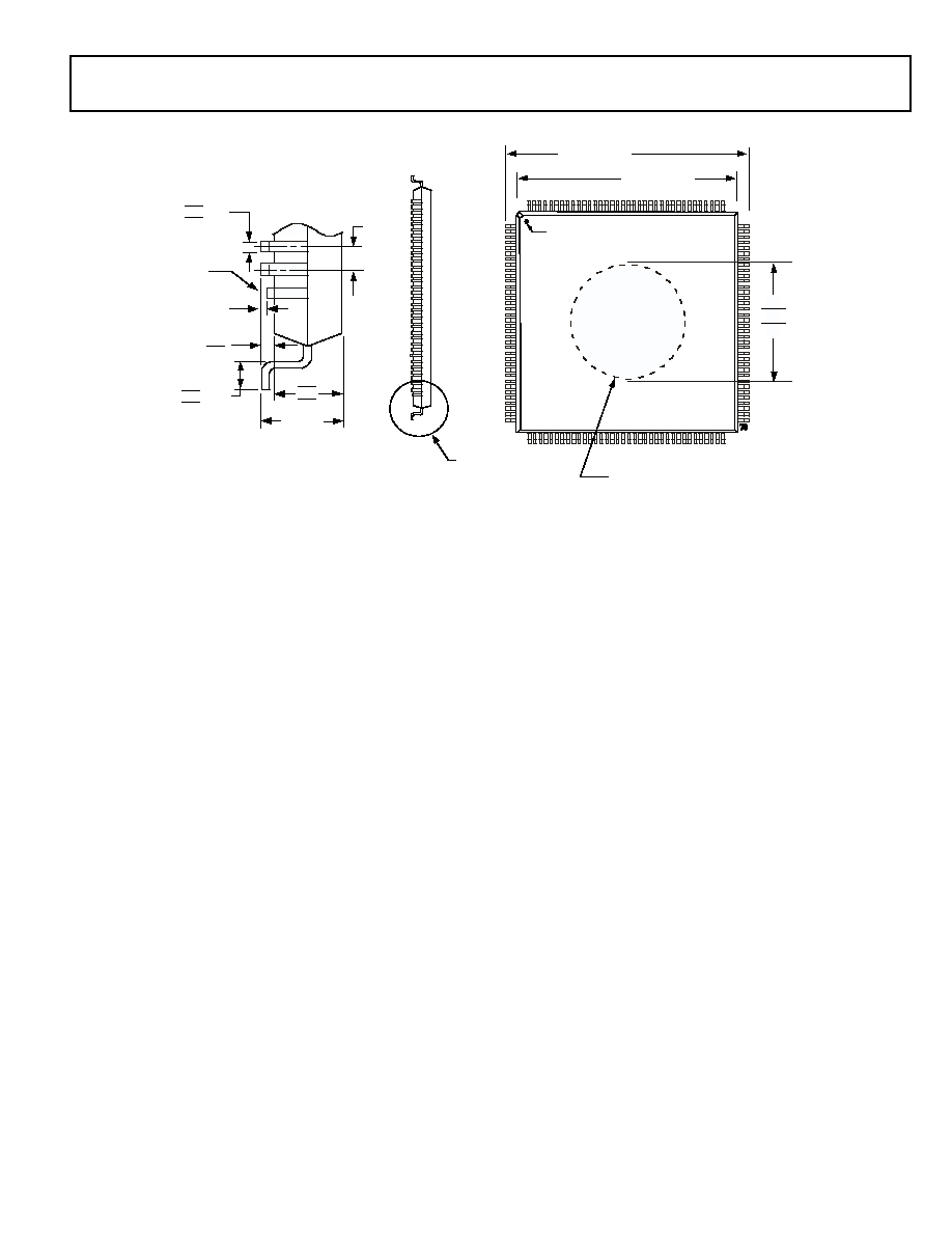
ADSP-21364
Preliminary Technical Data
Rev. PrB
|
Page 51 of 52
|
September 2004
Figure 44. 144-Lead Integrated Heatsink LQFP (SQ-144-3)
SEATING
PLANE
1.60 MAX
0.15
0.05
0. 08 MAX (LEAD
COPLANARITY)
1. 45
1. 40
1. 35
0.27
0.22
0.17
TYP
0.50
BSC
TYP
(LEAD
PI TCH)
DETAIL A
DE TAIL A
0.75
0.60 TYP
0.45
1
3 6
3 7
72
108
144
10 9
TOP VIE W (P INS DO WN)
22.00 BSC SQ
20. 00 BSC SQ
NOTES:
1. DIMENSIONS ARE IN MILLIMETERS AND COMPLY WITH
JEDEC STANDARD MS-026-BFB-HD.
2. ACTUAL PO SITION O F EACH LEAD IS WITHIN 0.08 OF ITS
IDEAL PO SITIO N, WHEN MEASURED I N THE LATERAL DIRECTI ON.
3. CENTER DIMENSIO NS ARE NOMINAL.
4. HEATSLUG IS COINCIDENT WI TH BO TTO M SURFACE AND DOES
NOT PROTRUDE BEYOND IT.
PIN 1 INDI CA TOR
HEATSLUG ON BOTTOM
(NOTE 4)
DIA
12.71
13.21
13.71
Rev. PrB
|
Page 52 of 52
|
September 2004
ADSP-21364
Preliminary Technical Data
© 2004 Analog Devices, Inc. All rights reserved. Trademarks and
registered trademarks are the property of their respective owners.
ORDERING GUIDE
Analog Devices offers a wide variety of audio algorithms and combinations to run on the ADSP-21364 processor. These products are sold
as part of a chip set, bundled with necessary application software under special part numbers. For a complete list, visit our web site at
www.analog.com/SHARC
.
These products also may contain 3rd party IPs that may require users to have authorization from the respective IP holders to receive them.
Royalty for use of the 3rd party IPs may also be payable by users.
Part Number
1,
2,
3
1
Z indicates Lead Free package. For more information about lead free package offerings, please visit www.analog.com.
2
See
Thermal Characteristics on Page 44
for information on package thermal specifications.
3
See EngineertoEngineer Note (EE TBD) for further information.
Ambient
Temperature
Range
°C
Instruction
Rate
On-Chip
SRAM
ROM
Operating Voltage
Internal/External
Volts
Package
ADSP-21364SKBCZENG
0 to 70
333MHz
3M bit
4M bit
1.2/3.3
136 Mini-BGA Pb-free
ADSP-21364SKBC-ENG
0 to 70
333MHz
3M bit
4M bit
1.2/3.3
136 Mini-BGA
ADSP-21364SKSQZENG
0 to 70
333MHz
3M bit
4M bit
1.2/3.3
144 INTHS LQFP Pb-free
ADSP-21364SKSQ-ENG
0 to 70
333MHz
3M bit
4M bit
1.2/3.3
144 INTHS LQFP
ADSP-21364SBBCZENG
4
4
PCB must have thermal vias. See
Thermal Characteristics on Page 44
. For more information see JEDEC Standard JESD51-9.
40 to 85
333MHz
3M bit
4M bit
1.2/3.3
136 Mini-BGA Pb-free
ADSP-21364SBBC-ENG
4
40 to 85
333MHz
3M bit
4M bit
1.2/3.3
136 Mini-BGA
ADSP-21364SBSQZENG
5
5
Heat slug must be soldered to the PCB. See
Thermal Characteristics on Page 44
. For more information see JEDEC Standard JESD51-5.
40 to 85
333MHz
3M bit
4M bit
1.2/3.3
144 INTHS LQFP Pb-free
ADSP-21364SBSQ-ENG
5
40 to 85
333MHz
3M bit
4M bit
1.2/3.3
144 INTHS LQFP
ADSP-21364SCSQZENG
5
40 to 105
200MHz
3M bit
4M bit
1.0/3.3
144 INTHS LQFP Pb-free
ADSP-21364SCSQ-ENG
5
40 to 105
200MHz
3M bit
4M bit
1.0/3.3
144 INTHS LQFP
PR04624-0-10/04(PrB)
Document Outline