ADSP-21375 SHARC® Processor Preliminary Data Sheet (Rev. PrB)
a
Preliminary Technical Data
SHARC and the SHARC logo are registered trademarks of Analog Devices, Inc.
SHARC
®
Processor
ADSP-21375
Rev. PrB
Information furnished by Analog Devices is believed to be accurate and reliable.
However, no responsibility is assumed by Analog Devices for its use, nor for any
infringements of patents or other rights of third parties that may result from its use.
Specifications subject to change without notice. No license is granted by implication
or otherwise under any patent or patent rights of Analog Devices. Trademarks and
registered trademarks are the property of their respective companies.
One Technology Way, P.O. Box 9106, Norwood, MA 02062-9106 U.S.A.
Tel: 781.329.4700
www.analog.com
Fax: 781.326.8703
© 2005 Analog Devices, Inc. All rights reserved.
SUMMARY
High performance 32-bit/40-bit floating point processor
optimized for high performance audio processing
Single-instruction, multiple-data (SIMD) computational
architecture
On-chip memory--0.5M bit of on-chip SRAM and a dedicated
2M bit of on-chip mask-programmable ROM
Code compatible with all other members of the SHARC family
The ADSP-21375 is available with a 266 MHz core instruction
rate with unique audio centric peripherals such as the digi-
tal applications interface, serial ports, precision clock
generators and more. For complete ordering information,
see
Ordering Guide on Page 42
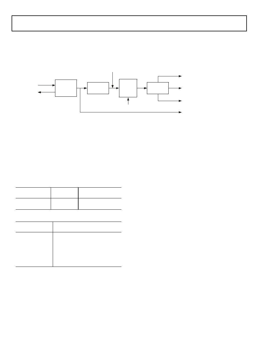
Figure 1. Functional Block Diagram
24
11
16
SDRAM
CO NTRO LLER
3
7
ASYNCHRONOUS
MEMO RY
INTERFACE
C
O
N
T
R
O
L
P
I
N
S
ADDRESS
DATA
CONTROL
EXTERNAL PORT
FLAGS4-15
SPI PORT (2)
TIMERS (2)
UART (1)
DP
I
R
O
U
T
I
NG
UN
I
T
DIGITAL PERIP HERAL INTE RFACE
GP IO FLAGS/
IRQ/TIMEXP
4
SERIAL PORTS (4)
I NP UT DATA POR T/
PDAP
DA
I
R
O
U
T
I
N
G
U
N
I
T
DIGITAL APPLICATIONS INTERFACE
I OD(32)
ADDR
DATA
IO A(24)
4 BLOCKS O F
ON-CHIP MEMORY
0. 5M BIT RAM, 2M BIT ROM
PM DA TA B U S
D M D A TA B U S
32
P M A D D RE SS BU S
DM A DD R ES S B U S
6 4
PX REGISTER
PROCESSING
ELEMENT
(PEY)
PROCESS ING
ELEMENT
(PEX)
TI MER
INSTRUCTIO N
CACHE
32 X 48-BI T
DAG 1
8X4X32
CORE PRO CESSOR
PROGRAM
SE QUENCER
DMA CONTROLLER
(24 CHANNELS )
MEMO RY-TO-MEMORY
DMA (2)
S
IOP REGISTER (MEMORY MAPPED)
CONTRO L, STATUS, & DATA BUFFERS
JTAG T EST & EMULATI ON
DAG2
8X4X32
I/O PROCESSOR
DAI PINS
DPI PINS
6 4
3 2
14
20
PRECISION CLO CK
GENERATORS (4)
TWO WIRE
INTERFACE
32
64

Rev. PrB
|
Page 2 of 42
|
December 2005
ADSP-21375
Preliminary Technical Data
KEY FEATURES PROCESSOR CORE
At 266 MHz (3.75 ns) core instruction rate, the ADSP-21375
performs 1.596 GFLOPs/533 MMACs
0.5M bit on-chip, SRAM for simultaneous access by the core
processor and DMA
2M bit on-chip, mask-programmable, ROM
Dual data address generators (DAGs) with modulo and bit-
reverse addressing
Zero-overhead looping with single-cycle loop setup, provid-
ing efficient program sequencing
Single instruction multiple data (SIMD) architecture
provides:
Two computational processing elements
Concurrent execution
Code compatibility with other SHARC family members at
the assembly level
Parallelism in buses and computational units allows: Sin-
gle cycle executions (with or without SIMD) of a multiply
operation, an ALU operation, a dual memory read or
write, and an instruction fetch
Transfers between memory and core at a sustained 4.25G
byte/sec bandwidth at 266 MHz core instruction rate
INPUT/OUTPUT FEATURES
DMA controller supports:
24 DMA channels for transfers between ADSP-21375 inter-
nal memory and a variety of peripherals
32-bit DMA transfers at peripheral clock speed, in parallel
with full-speed processor execution
16-Bit wide external port provides glueless connection to
both synchronous (SDRAM) and asynchronous memory
devices
Programmable wait state options: 2 to 31 SDCLK cycles
Delay-line DMA engine maintains circular buffers in exter-
nal memory with tap/offset based reads
SDRAM accesses at 133 MHz and asynchronous accesses at
42.25 MHz
4 memory select lines allows multiple external memory
devices
Digital applications interface (DAI) includes four serial ports,
four precision clock generators, an input data port, and a
signal routing unit
Digital peripheral interface (DPI) includes, two timers, one
UART, and two SPI ports, and a two wire interface port
Outputs of PCG's C and D can be driven on to DPI pins
Four dual data line serial ports that operate at up to 33M
bits/s on each data line -- each has a clock, frame sync and
two data lines that can be configured as either a receiver or
transmitter pair
TDM support for telecommunications interfaces including
128 TDM channel support for newer telephony interfaces
such as H.100/H.110
Up to 8 TDM stream support, each with 128 channels per
frame
Companding selection on a per channel basis in TDM mode
Input data port, configurable as eight channels of serial data
or seven channels of serial data and up to a 20-bit wide
parallel data channel
Signal routing unit provides configurable and flexible con-
nections between all DAI/DPI components
2 Muxed Flag/IRQ lines
1 Muxed Flag/Timer expired line /MS pin
1 Muxed Flag/IRQ /MS pin
ROM Based Security features include:
JTAG access to memory permitted with a 64-bit key
Protected memory regions that can be assigned to limit
access under program control to sensitive code
PLL has a wide variety of software and hardware multi-
plier/divider ratios
Dual voltage: 3.3 V I/O, 1.2 V core
Available in 208-lead MQFP Package (see
Ordering Guide on
Page 42
)

ADSP-21375
Preliminary Technical Data
Rev. PrB
|
Page 3 of 42
|
December 2005
TABLE OF CONTENTS
Summary ................................................................1
Key Features Processor Core ..................................2
Input/Output Features ............................................2
General Description ..................................................4
ADSP-21375 Family Core Architecture .......................4
ADSP-21375 Memory .............................................5
External Memory ...................................................5
ADSP-21375 Input/Output Features ...........................7
System Design .......................................................9
Development Tools ................................................9
Pin Function Descriptions ........................................ 12
Data Modes ........................................................ 15
Boot Modes ........................................................ 15
Core Instruction Rate to CLKIN Ratio Modes ............. 15
ADSP-21375 Specifications ....................................... 16
Recommended Operating Conditions ....................... 16
Electrical Characteristics ........................................ 16
Absolute Maximum Ratings ................................... 17
Maximum Power Dissipation ................................. 17
ESD Sensitivity .................................................... 17
Timing Specifications ........................................... 17
Output Drive Currents .......................................... 39
Test Conditions ................................................... 39
Capacitive Loading ............................................... 39
Thermal Characteristics ........................................ 40
208-Lead MQFP Pinout ............................................ 41
Package Dimensions ................................................ 42
Ordering Guide ...................................................... 42
REVISION HISTORY
12/05--Revision changed from PrA to PrB.
Modified
Figure 1, Functional Block Diagram,..................1
SDRAM bank address example in last paragraph of
SDRAM
Controller ...............................................................6
Added
Two Wire Interface Port (TWI) ..........................9
Added
TWI Controller Timing .................................. 37

Rev. PrB
|
Page 4 of 42
|
December 2005
ADSP-21375
Preliminary Technical Data
GENERAL DESCRIPTION
The ADSP-21375 SHARC processor is a members of the SIMD
SHARC family of DSPs that feature Analog Devices' Super Har-
vard Architecture. The ADSP-21375 is source code compatible
with the ADSP-2126x, ADSP-2136x, and ADSP-2116x DSPs as
well as with first generation ADSP-2106x SHARC processors in
SISD (single-instruction, single-data) mode. The ADSP-21375
is a 32-bit/40-bit floating point processors optimized for high
performance automotive audio applications with its large on-
chip SRAM and mask-programmable ROM, multiple internal
buses to eliminate I/O bottlenecks, and an innovative digital
applications interface (DAI).
As shown in the functional block diagram
on Page 1
, the
ADSP-21375 uses two computational units to deliver a signifi-
cant performance increase over the previous SHARC processors
on a range of DSP algorithms. Fabricated in a state-of-the-art,
high speed, CMOS process, the ADSP-21375 processor achieves
an instruction cycle time of 3.75 ns at 266 MHz. With its SIMD
computational hardware, the ADSP-21375 can perform 1.596
GFLOPS running at 266 MHz.
Table 1
shows performance benchmarks for the ADSP-21375.
The ADSP-21375 continues SHARC's industry leading stan-
dards of integration for DSPs, combining a high performance
32-bit DSP core with integrated, on-chip system features.
The block diagram of the ADSP-21375
on Page 1
, illustrates the
following architectural features:
· Two processing elements, each of which comprises an
ALU, multiplier, shifter and data register file
· Data address generators (DAG1, DAG2)
· Program sequencer with instruction cache
· PM and DM buses capable of supporting four 32-bit data
transfers between memory and the core at every core pro-
cessor cycle
· Two programmable interval timers with external event
counter capabilities
· On-chip SRAM (0.5M bit)
· On-chip mask-programmable ROM (2M bit)
· JTAG test access port
The block diagram of the ADSP-21375
on Page 1
also illustrates
the following architectural features:
· DMA controller
· Four full duplex serial ports
· Digital applications interface that includes four precision
clock generators (PCG), an input data port (IDP), four
serial ports, eight serial interfaces, a 16-bit parallel input
port (PDAP), and a flexible signal routing unit (DAI SRU).
· Digital peripheral interface that includes two timers, one
UART, two serial peripheral interfaces (SPI), a two wire
interface (TWI), and a flexible signal routing unit (DPI
SRU).
ADSP-21375 FAMILY CORE ARCHITECTURE
The ADSP-21375 is code compatible at the assembly level with
the ADSP-2136x, ADSP-2126x, ADSP-21160 and ADSP-21161,
and with the first generation ADSP-2106x SHARC processors.
The ADSP-21375 shares architectural features with the ADSP-
2126x, ADSP-2136x, and ADSP-2116x SIMD SHARC proces-
sors, as detailed in the following sections.
SIMD Computational Engine
The ADSP-21375 contains two computational processing ele-
ments that operate as a single-instruction multiple-data (SIMD)
engine. The processing elements are referred to as PEX and PEY
and each contains an ALU, multiplier, shifter and register file.
PEX is always active, and PEY may be enabled by setting the
PEYEN mode bit in the MODE1 register. When this mode is
enabled, the same instruction is executed in both processing ele-
ments, but each processing element operates on different data.
This architecture is efficient at executing math intensive DSP
algorithms.
Entering SIMD mode also has an effect on the way data is trans-
ferred between memory and the processing elements. When in
SIMD mode, twice the data bandwidth is required to sustain
computational operation in the processing elements. Because of
this requirement, entering SIMD mode also doubles the band-
width between memory and the processing elements. When
using the DAGs to transfer data in SIMD mode, two data values
are transferred with each access of memory or the register file.
Independent, Parallel Computation Units
Within each processing element is a set of computational units.
The computational units consist of an arithmetic/logic unit
(ALU), multiplier, and shifter. These units perform all opera-
tions in a single cycle. The three units within each processing
element are arranged in parallel, maximizing computational
throughput. Single multifunction instructions execute parallel
ALU and multiplier operations. In SIMD mode, the parallel
ALU and multiplier operations occur in both processing ele-
Table 1. ADSP-21375 Benchmarks (at 266 MHz)
Benchmark Algorithm
Speed
(at 266 MHz)
1024 Point Complex FFT (Radix 4, with reversal) 34.5
s
FIR Filter (per tap)
1
1
Assumes two files in multichannel SIMD mode
1.88 ns
IIR Filter (per biquad)
1
7.5 ns
Matrix Multiply (pipelined)
[3x3] × [3x1]
[4x4] × [4x1]
16.91 ns
30.07 ns
Divide (y/×)
11.27 ns
Inverse Square Root
16.91 ns

ADSP-21375
Preliminary Technical Data
Rev. PrB
|
Page 5 of 42
|
December 2005
ments. These computation units support IEEE 32-bit single-
precision floating-point, 40-bit extended precision floating-
point, and 32-bit fixed-point data formats.
Data Register File
A general-purpose data register file is contained in each pro-
cessing element. The register files transfer data between the
computation units and the data buses, and store intermediate
results. These 10-port, 32-register (16 primary, 16 secondary)
register files, combined with the ADSP-2136x enhanced Har-
vard architecture, allow unconstrained data flow between
computation units and internal memory. The registers in PEX
are referred to as R0-R15 and in PEY as S0-S15.
Single-Cycle Fetch of Instruction and Four Operands
The ADSP-21375 features an enhanced Harvard architecture in
which the data memory (DM) bus transfers data and the pro-
gram memory (PM) bus transfers both instructions and data
(see
Figure 1 on page 1
). With the ADSP-21375's separate pro-
gram and data memory buses and on-chip instruction cache,
the processor can simultaneously fetch four operands (two over
each data bus) and one instruction (from the cache), all in a sin-
gle cycle.
Instruction Cache
The ADSP-21375 includes an on-chip instruction cache that
enables three-bus operation for fetching an instruction and four
data values. The cache is selective--only the instructions whose
fetches conflict with PM bus data accesses are cached. This
cache allows full-speed execution of core, looped operations
such as digital filter multiply-accumulates, and FFT butterfly
processing.
Data Address Generators With Zero-Overhead Hardware
Circular Buffer Support
The ADSP-21375's two data address generators (DAGs) are
used for indirect addressing and implementing circular data
buffers in hardware. Circular buffers allow efficient program-
ming of delay lines and other data structures required in digital
signal processing, and are commonly used in digital filters and
Fourier transforms. The two DAGs of the ADSP-21375 contain
sufficient registers to allow the creation of up to 32 circular buff-
ers (16 primary register sets, 16 secondary). The DAGs
automatically handle address pointer wraparound, reduce over-
head, increase performance, and simplify implementation.
Circular buffers can start and end at any memory location.
Flexible Instruction Set
The 48-bit instruction word accommodates a variety of parallel
operations, for concise programming. For example, the
ADSP-21375 can conditionally execute a multiply, an add, and a
subtract in both processing elements while branching and fetch-
ing up to four 32-bit values from memory--all in a single
instruction.
ADSP-21375 MEMORY
The ADSP-21375 adds the following architectural features to
the SIMD SHARC family core.
On-Chip Memory
The ADSP-21375 contains 0.5 megabits of internal RAM and
two megabits of internal mask-programmable ROM. Each block
can be configured for different combinations of code and data
storage (see
Table 2 on page 6
). Each memory block supports
single-cycle, independent accesses by the core processor and I/O
processor. The ADSP-21375 memory architecture, in combina-
tion with its separate on-chip buses, allow two data transfers
from the core and one from the I/O processor, in a single cycle.
The ADSP-21375's, SRAM can be configured as a maximum of
16K words of 32-bit data, 32K words of 16-bit data, 10.9K words
of 48-bit instructions (or 40-bit data), or combinations of differ-
ent word sizes up to 0.5 megabits. All of the memory can be
accessed as 16-bit, 32-bit, 48-bit, or 64-bit words. A 16-bit float-
ing-point storage format is supported that effectively doubles
the amount of data that may be stored on-chip. Conversion
between the 32-bit floating-point and 16-bit floating-point for-
mats is performed in a single instruction. While each memory
block can store combinations of code and data, accesses are
most efficient when one block stores data using the DM bus for
transfers, and the other block stores instructions and data using
the PM bus for transfers.
Using the DM bus and PM buses, with one bus dedicated to
each memory block, assures single-cycle execution with two
data transfers. In this case, the instruction must be available in
the cache.
EXTERNAL MEMORY
The external port on the ADSP-21375 SHARC provides a high
performance, glueless interface to a wide variety of industry-
standard memory devices. The 16-bit wide bus may be used to
interface to synchronous and/or asynchronous memory devices
through the use of it's separate internal memory controllers: the
first is an SDRAM controller for connection of industry-stan-
dard synchronous DRAM devices and DIMMs (Dual Inline
Memory Module), while the second is an asynchronous mem-
ory controller intended to interface to a variety of memory
devices. Four memory select pins enable up to four separate
devices to coexist, supporting any desired combination of syn-
chronous and asynchronous device types. Non SDRAM
external memory address space is shown in
Table 3
.
External Memory Execution
In the ADSP-21375, the program sequencer can execute code
directly from external memory (SRAM, SDRAM). This allows a
reduction in internal memory size, thereby reducing the die
area. It also allows for faster code development. With external
execution, programs run at slower speeds since 48-bit instruc-
tions are fetched in parts from a 16-bit external bus coupled
with the inherent latency of fetching instructions from SDRAM.
Fetching instructions from external memory generally take
three core clock cycles per instruction.
Rev. PrB
|
Page 6 of 42
|
December 2005
ADSP-21375
Preliminary Technical Data
SDRAM Controller
The SDRAM controller provides an interface to up to four sepa-
rate banks of industry-standard SDRAM devices or DIMMs, at
speeds up to f
SCLK
. Fully compliant with the SDRAM standard,
each bank can has it's own memory select line (MS0MS3), and
can be configured to contain between 16M bytes and
128M bytes of memory. SDRAM external memory address
space is shown in
Table 4
.
The controller maintains all of the banks as a contiguous
address space so that the processor sees this as a single address
space, even if different size devices are used in the different
banks.
A set of programmable timing parameters is available to config-
ure the SDRAM banks to support slower memory devices. The
memory banks can be configured as 16 bits wide.
Table 2. ADSP-21375 Internal Memory Space
IOP Registers 0x0000 00000x0003 FFFF
Long Word (64 bits)
Extended Precision Normal or
Instruction Word (48 bits)
Normal Word (32 bits)
Short Word (16 bits)
BLOCK 0 ROM
0x0004 00000x0004 3FFF
BLOCK 0 ROM
0x0008 00000x0008 5554
BLOCK 0 ROM
0x0008 00000x0008 7FFF
BLOCK 0 ROM
0x0010 00000x0010 FFFF
Reserved
0x0004 40000x0004 BFFF
Reserved
0x0008 55550x0008 FFFF
Reserved
0x000880000x00097FFF
Reserved
0x0011 00000x0012 FFFF
BLOCK 0 RAM
0x0004 C0000x0004C7FF
BLOCK 0 RAM
0x0009 00000x0009 0AAA
BLOCK 0 RAM
0x0009 80000x0009 8FFF
BLOCK 0 RAM
0x0013 00000x0013 1FFF
Reserved
0x0004 C8000x0004 FFFF
Reserved
0x0009 0AAB0x0009 5554
Reserved
0x0009 90000x0009 FFFF
Reserved
0x0013 20000x0013 FFFF
BLOCK 1 ROM
0x0005 00000x0005 3FFF
BLOCK 1 ROM
0x000A 00000x000A 5554
BLOCK 1 ROM
0x000A 00000x000A 7FFF
BLOCK 1 ROM
0x0014 00000x0014 FFFF
Reserved
0x0005 40000x0005 BFFF
Reserved
0x000A 55550x000A FFFF
Reserved
0x000A 80000x000B 7FFF
Reserved
0x0015 00000x0016 FFFF
BLOCK 1 RAM
0x0005 C0000x0005 C7FF
BLOCK 1 RAM
0x000B 00000x000B 0AAA
BLOCK 1 RAM
0x000B 80000x000B 8FFF
BLOCK 1 RAM
0x0017 00000x0017 1FFF
Reserved
0x0005 C80000x0005 FFFF
Reserved
0x000B 0AAB0X000B 5554
Reserved
0x000B 90000x000B FFFF
Reserved
0x0017 20000x0017 FFFF
BLOCK 2 RAM
0x0006 00000x0006 07FF
BLOCK 2 RAM
0x000C 00000x000C 0AAA
BLOCK 2 RAM
0X000C 0000 - 0X000C 3FFF
BLOCK 2 RAM
0x0018 00000x0018 1FFF
Reserved
0x0006 08000x0006 1FFF
Reserved
0x000C 0AAB0x000C 3FFF
Reserved
0x000C 10000x000C 1FFF
Reserved
0x0018 20000x0018 7FFF
Reserved
0x0006 20000x0006 FFFF
Reserved
0x000D 40000x000D 5554
Reserved
0x000C 40000x000D FFFF
Reserved
0x0018 80000x001B FFFF
BLOCK 3 RAM
0x0007 00000x0007 07FF
BLOCK 3 RAM
0x000E 00000x000E 0AAA
BLOCK 3 RAM
0x000E 00000x000E 0FFF
BLOCK 3 RAM
0x001C 00000x001C 1FFF
Reserved
0x0007 08000x0007 1FFF
Reserved
0x000E 0AAB0x000C 3FFF
Reserved
0x000E 10000x000E 3FFF
Reserved
0x001C 20000x001C 7FFF
Reserved
0x0007 20000x0007 FFFF
Reserved
0x000F 40000x000F 5554
Reserved
0x000E 40000x000F FFFF
Reserved
0x001C 80000x001F FFFF
Table 3. External Memory for Non SDRAM Addresses
Bank
Size in
words
Address Range
Bank 0
14M
0x0020 0000 0x00FF FFFF
Bank 1
16M
0x0400 0000 0x04FF FFFF
Bank 2
16M
0x0800 0000 0x08FF FFFF
Bank 3
16M
0x0C00 0000 0x0CFF FFFF
ADSP-21375
Preliminary Technical Data
Rev. PrB
|
Page 7 of 42
|
December 2005
The SDRAM controller address, data, clock, and command pins
can drive loads up to 30 pF. For larger memory systems, the
SDRAM controller external buffer timing should be selected
and external buffering should be provided so that the load on
the SDRAM controller pins does not exceed 30 pF.
Note that the external memory bank addresses shown are for
normal word accesses. If 48-bit instructions are placed in any
such bank (with two instructions packed into three 32-bit loca-
tions), then care must be taken to map data buffers in the same
bank. For example, if 2K instructions are placed starting at the
bank 0 base address (0x0020 0000), then the data buffers can be
placed starting at an address that is offset by 3K words
(0x0020 0C00).
Asynchronous Controller
The asynchronous memory controller provides a configurable
interface for up to four separate banks of memory or I/O
devices. Each bank can be independently programmed with dif-
ferent timing parameters, enabling connection to a wide variety
of memory devices including SRAM, ROM, flash, and EPROM,
as well as I/O devices that interface with standard memory con-
trol lines. Bank0 occupies a 14.7M word window and banks 1, 2,
and 3 occupy a 16M word window in the processor's address
space but, if not fully populated, these windows are not made
contiguous by the memory controller logic. The banks can also
be configured as 8-bit or 16-bit wide buses for ease of interfac-
ing to a range of memories and I/O devices tailored either to
high performance or to low cost and power.
The asynchronous memory controller is capable of a maximum
throughput of 88M bytes/sec using a 44MHz external bus speed.
Other features include 8 to 32-bit and 16 to 32-bit packing and
unpacking, booting from bank select 1, and support for delay
line DMA.
ADSP-21375 INPUT/OUTPUT FEATURES
The ADSP-21375 I/O processor provides 24 channels of DMA,
as well as an extensive set of peripherals. These include a 20 pin
digital applications interface which controls:
· Four serial ports
· Four precision clock generators
· Internal data port/parallel data acquisition port
The ADSP-21375 processor also contains a 14 pin digital
peripheral interface which controls:
· Two general-purpose timers
· Two serial peripheral interfaces
· One universal asynchronous receiver/transmitter (UART)
· An I
2
C compatible two wire interface
DMA Controller
The ADSP-21375's on-chip DMA controller allows data trans-
fers without processor intervention. The DMA controller
operates independently and invisibly to the processor core,
allowing DMA operations to occur while the core is simulta-
neously executing its program instructions. DMA transfers can
occur between the ADSP-21375's internal memory and its serial
ports, the SPI-compatible (serial peripheral interface) ports, the
IDP (input data port), the parallel data acquisition port (PDAP)
or the UART. Twenty-four channels of DMA are available on
the ADSP-21375--eight via the serial ports, eight via the input
data port, two for the UART, two for the SPI interface, two for
the external port, and two for memory-to-memory transfers.
Programs can be downloaded to the ADSP-21375 using DMA
transfers. Other DMA features include interrupt generation
upon completion of DMA transfers, and DMA chaining for
automatic linked DMA transfers.
Delay Line DMA
The ADSP-21375 processor provides delay line DMA function-
ality. This allows processor reads and writes to external Delay
Line Buffers (and hence to external memory) with limited core
interaction.
Digital Applications Interface (DAI)
The digital applications interface (DAI) provides the ability to
connect various peripherals to any of the DSPs DAI pins
(DAI_P201).
Programs make these connections using the signal routing unit
(SRU), shown in
Figure 1
.
The SRU is a matrix routing unit (or group of multiplexers) that
enables the peripherals provided by the DAI to be intercon-
nected under software control. This allows easy use of the DAI
associated peripherals for a much wider variety of applications
by using a larger set of algorithms than is possible with non con-
figurable signal paths.
The DAI also includes four serial ports, four precision clock
generators (PCG), and an input data port (IDP). The IDP pro-
vides an additional input path to the ADSP-21375 core,
configurable as either eight channels of I
2
S serial data or as
seven channels plus a single 20-bit wide synchronous parallel
data acquisition port. Each data channel has its own DMA
channel that is independent from the ADSP-21375's serial ports.
Serial Ports
The ADSP-21375 features four synchronous serial ports that
provide an inexpensive interface to a wide variety of digital and
mixed-signal peripheral devices such as Analog Devices'
AD183x family of audio codecs, ADCs, and DACs. The serial
Table 4. External Memory for SDRAM Addresses
Bank
Size in
words
Address Range
Bank 0
62M
0x0020 0000 0x03FF FFFF
Bank 1
64M
0x0400 0000 0x07FF FFFF
Bank 2
64M
0x0800 0000 0x0BFF FFFF
Bank 3
64M
0x0C00 0000 0x0FFF FFFF

Rev. PrB
|
Page 8 of 42
|
December 2005
ADSP-21375
Preliminary Technical Data
ports are made up of two data lines, a clock and frame sync. The
data lines can be programmed to either transmit or receive and
each data line has a dedicated DMA channel.
Serial ports are enabled via eight programmable and simulta-
neous receive or transmit pins that support up to 16 transmit or
16 receive channels of audio data when all four SPORTS are
enabled, or four full duplex TDM streams of 128 channels per
frame.
The serial ports operate at a maximum data rate of 50M bits/s.
Serial port data can be automatically transferred to and from
on-chip memory via dedicated DMA channels. Each of the
serial ports can work in conjunction with another serial port to
provide TDM support. One SPORT provides two transmit sig-
nals while the other SPORT provides the two receive signals.
The frame sync and clock are shared.
Serial ports operate in five modes:
· Standard DSP serial mode
· Multichannel (TDM) mode with support for Packed I
2
S
mode
· I
2
S mode
· Packed I
2
S mode
· Left-justified sample pair mode
Left-justified sample pair mode is a mode where in each frame
sync cycle two samples of data are transmitted/received--one
sample on the high segment of the frame sync, the other on the
low segment of the frame sync. Programs have control over var-
ious attributes of this mode.
Each of the serial ports supports the left-justified sample pair
and I
2
S protocols (I
2
S is an industry standard interface com-
monly used by audio codecs, ADCs and DACs such as the
Analog Devices AD183x family), with two data pins, allowing
four left-justified sample pair or I
2
S channels (using two stereo
devices) per serial port, with a maximum of up to 32 I
2
S chan-
nels. The serial ports permit little-endian or big-endian
transmission formats and word lengths selectable from 3 bits to
32 bits. For the left-justified sample pair and I
2
S modes, data-
word lengths are selectable between 8 bits and 32 bits. Serial
ports offer selectable synchronization and transmit modes as
well as optional -law or A-law companding selection on a per
channel basis. Serial port clocks and frame syncs can be inter-
nally or externally generated.
The serial ports also contain frame sync error detection logic
where the serial ports detect frame syncs that arrive early (for
example frame syncs that arrive while the transmission/recep-
tion of the previous word is occurring). All the serial ports also
share one dedicated error interrupt.
Digital Peripheral Interface (DPI)
The digital peripheral interface provides connections to two
serial peripheral interface ports (SPI), one universal asynchro-
nous receiver-transmitter (UART), 12 flags, a two wire interface
(TWI), and two general-purpose timers.
Serial Peripheral (Compatible) Interface
The ADSP-21375 SHARC processor contains two serial periph-
eral interface ports (SPIs). The SPI is an industry standard
synchronous serial link, enabling the ADSP-21375 SPI compati-
ble port to communicate with other SPI compatible devices. The
SPI consists of two data pins, one device select pin, and one
clock pin. It is a full-duplex synchronous serial interface, sup-
porting both master and slave modes. The SPI port can operate
in a multimaster environment by interfacing with up to four
other SPI compatible devices, either acting as a master or slave
device. The ADSP-21375 SPI compatible peripheral implemen-
tation also features programmable baud rate and clock phase
and polarities. The ADSP-21375 SPI compatible port uses open
drain drivers to support a multimaster configuration and to
avoid data contention.
UART Port
The ADSP-21375 processor provides a full-duplex Universal
Asynchronous Receiver/Transmitter (UART) port, which is
fully compatible with PC-standard UARTs. The UART port
provides a simplified UART interface to other peripherals or
hosts, supporting full-duplex, DMA-supported, asynchronous
transfers of serial data. The UART also has multiprocessor com-
munication capability using 9-bit address detection. This allows
it to be used in multidrop networks through the RS-485 data
interface standard. The UART port also includes support for 5
to 8 data bits, 1 or 2 stop bits, and none, even, or odd parity. The
UART port supports two modes of operation:
· PIO (programmed I/O) The processor sends or receives
data by writing or reading I/O-mapped UART registers.
The data is double-buffered on both transmit and receive.
· DMA (direct memory access) The DMA controller trans-
fers both transmit and receive data. This reduces the
number and frequency of interrupts required to transfer
data to and from memory. The UART has two dedicated
DMA channels, one for transmit and one for receive. These
DMA channels have lower default priority than most DMA
channels because of their relatively low service rates.
The UART port's baud rate, serial data format, error code gen-
eration and status, and interrupts are programmable:
· Supporting bit rates ranging from (f
SCLK
/ 1,048,576) to
(f
SCLK
/16) bits per second.
· Supporting data formats from 7 to12 bits per frame.
· Both transmit and receive operations can be configured to
generate maskable interrupts to the processor.
where the 16-bit UART_Divisor comes from the DLH register
(most significant 8 bits) and DLL register (least significant
8 bits).
In conjunction with the general-purpose timer functions, auto-
baud detection is supported.

ADSP-21375
Preliminary Technical Data
Rev. PrB
|
Page 9 of 42
|
December 2005
Timers
The ADSP-21375 has a total of three timers: a core timer that
can generate periodic software interrupts and two general pur-
pose timers that can generate periodic interrupts and be
independently set to operate in one of three modes:
· Pulse waveform generation mode
· Pulse width count/capture mode
· External event watchdog mode
The core timer can be configured to use FLAG3 as a timer
expired signal, and each general purpose timer has one bidirec-
tional pin and four registers that implement its mode of
operation: a 6-bit configuration register, a 32-bit count register,
a 32-bit period register, and a 32-bit pulse width register. A sin-
gle control and status register enables or disables both general
purpose timers independently.
Two Wire Interface Port (TWI)
The TWI is a bi-directional 2-wire, serial bus used to move 8-bit
data while maintaining compliance with the I
2
C bus protocol.
The TWI master incorporates the following features:
· Simultaneous master and slave operation on multiple
device systems with support for multi master data
arbitration
· Digital filtering and timed event processing
· 7 and 10 bit addressing
· 100K bits/s and 400K bits/s data rates
· Low interrupt rate
ROM Based Security
The ADSP-21375 has a ROM security feature that provides
hardware support for securing user software code by preventing
unauthorized reading from the internal code when enabled.
When using this feature, the processor does not boot-load any
external code, executing exclusively from internal SRAM/ROM.
Additionally, the processor is not freely accessible via the JTAG
port. Instead, a unique 64-bit key, which must be scanned in
through the JTAG or Test Access Port will be assigned to each
customer. The device will ignore a wrong key. Emulation fea-
tures and external boot modes are only available after the
correct key is scanned.
SYSTEM DESIGN
The following sections provide an introduction to system design
options and power supply issues.
Program Booting
The internal memory of the ADSP-21375 boots at system
power-up from an 8-bit EPROM via the external port, an SPI
master, an SPI slave. Booting is determined by the boot configu-
ration (BOOTCFG10) pins (see
Table 7 on page 15
). Selection
of the boot source is controlled via the SPI as either a master or
slave device, or it can immediately begin executing from ROM.
Power Supplies
The ADSP-21375 has separate power supply connections for the
internal (V
DDINT
), and external (V
DDEXT
) power supplies. The
internal supplies must meet the 1.2V requirement. The external
supply must meet the 3.3V requirement. All external supply
pins must be connected to the same power supply.
Target Board JTAG Emulator Connector
Analog Devices DSP Tools product line of JTAG emulators uses
the IEEE 1149.1 JTAG test access port of the ADSP-21375 pro-
cessor to monitor and control the target board processor during
emulation. Analog Devices DSP Tools product line of JTAG
emulators provides emulation at full processor speed, allowing
inspection and modification of memory, registers, and proces-
sor stacks. The processor's JTAG interface ensures that the
emulator will not affect target system loading or timing.
For complete information on Analog Devices' SHARC DSP
Tools product line of JTAG emulator operation, see the appro-
priate "Emulator Hardware User's Guide".
DEVELOPMENT TOOLS
The ADSP-21375 is supported with a complete set of
CROSSCORE
®
software and hardware development tools,
including Analog Devices emulators and VisualDSP++
®
devel-
opment environment. The same emulator hardware that
supports other SHARC processors also fully emulates the
ADSP-21375.
The VisualDSP++ project management environment lets pro-
grammers develop and debug an application. This environment
includes an easy to use assembler (which is based on an alge-
braic syntax), an archiver (librarian/library builder), a linker, a
loader, a cycle-accurate instruction-level simulator, a C/C++
compiler, and a C/C++ runtime library that includes DSP and
mathematical functions. A key point for these tools is C/C++
code efficiency. The compiler has been developed for efficient
translation of C/C++ code to DSP assembly. The SHARC has
architectural features that improve the efficiency of compiled
C/C++ code.
The VisualDSP++ debugger has a number of important fea-
tures. Data visualization is enhanced by a plotting package that
offers a significant level of flexibility. This graphical representa-
tion of user data enables the programmer to quickly determine
the performance of an algorithm. As algorithms grow in com-
plexity, this capability can have increasing significance on the
designer's development schedule, increasing productivity. Sta-
tistical profiling enables the programmer to non intrusively poll
the processor as it is running the program. This feature, unique
to VisualDSP++, enables the software developer to passively
gather important code execution metrics without interrupting
the real-time characteristics of the program. Essentially, the
developer can identify bottlenecks in software quickly and effi-
ciently. By using the profiler, the programmer can focus on
those areas in the program that impact performance and take
corrective action.

Rev. PrB
|
Page 10 of 42
|
December 2005
ADSP-21375
Preliminary Technical Data
Debugging both C/C++ and assembly programs with the
VisualDSP++ debugger, programmers can:
· View mixed C/C++ and assembly code (interleaved source
and object information)
· Insert breakpoints
· Set conditional breakpoints on registers, memory,
and stacks
· Trace instruction execution
· Perform linear or statistical profiling of program execution
· Fill, dump, and graphically plot the contents of memory
· Perform source level debugging
· Create custom debugger windows
The VisualDSP++ IDDE lets programmers define and manage
DSP software development. Its dialog boxes and property pages
let programmers configure and manage all of the SHARC devel-
opment tools, including the color syntax highlighting in the
VisualDSP++ editor. This capability permits programmers to:
· Control how the development tools process inputs and
generate outputs
· Maintain a one-to-one correspondence with the tool's
command line switches
The VisualDSP++ Kernel (VDK) incorporates scheduling and
resource management tailored specifically to address the mem-
ory and timing constraints of DSP programming. These
capabilities enable engineers to develop code more effectively,
eliminating the need to start from the very beginning, when
developing new application code. The VDK features include
Threads, Critical and Unscheduled regions, Semaphores,
Events, and Device flags. The VDK also supports Priority-based,
Preemptive, Cooperative, and Time-Sliced scheduling
approaches. In addition, the VDK was designed to be scalable. If
the application does not use a specific feature, the support code
for that feature is excluded from the target system.
Because the VDK is a library, a developer can decide whether to
use it or not. The VDK is integrated into the VisualDSP++
development environment, but can also be used via standard
command line tools. When the VDK is used, the development
environment assists the developer with many error-prone tasks
and assists in managing system resources, automating the gen-
eration of various VDK based objects, and visualizing the
system state, when debugging an application that uses the VDK.
VisualDSP++ Component Software Engineering (VCSE) is
Analog Devices' technology for creating, using, and reusing
software components (independent modules of substantial
functionality) to quickly and reliably assemble software applica-
tions. Download components from the Web and drop them into
the application. Publish component archives from within
VisualDSP++. VCSE supports component implementation in
C/C++ or assembly language.
Use the Expert Linker to visually manipulate the placement of
code and data on the embedded system. View memory utiliza-
tion in a color-coded graphical form, easily move code and data
to different areas of the processor or external memory with the
drag of the mouse, examine run time stack and heap usage. The
Expert Linker is fully compatible with the existing Linker Defi-
nition File (LDF), allowing the developer to move between the
graphical and textual environments.
In addition to the software and hardware development tools
available from Analog Devices, third parties provide a wide
range of tools supporting the SHARC processor family. Hard-
ware tools include SHARC processor PC plug-in cards. Third
party software tools include DSP libraries, real-time operating
systems, and block diagram design tools.
Designing an Emulator-Compatible DSP Board (Target)
The Analog Devices family of emulators are tools that every
DSP developer needs to test and debug hardware and software
systems. Analog Devices has supplied an IEEE 1149.1 JTAG
Test Access Port (TAP) on each JTAG DSP. Nonintrusive in-
circuit emulation is assured by the use of the processor's JTAG
interface--the emulator does not affect target system loading or
timing. The emulator uses the TAP to access the internal fea-
tures of the processor, allowing the developer to load code, set
breakpoints, observe variables, observe memory, and examine
registers. The processor must be halted to send data and com-
mands, but once an operation has been completed by the
emulator, the DSP system is set running at full speed with no
impact on system timing.
To use these emulators, the target board must include a header
that connects the DSP's JTAG port to the emulator.
For details on target board design issues including mechanical
layout, single processor connections, signal buffering, signal ter-
mination, and emulator pod logic, see the EE-68: Analog Devices
JTAG Emulation Technical Reference on the Analog Devices
website (
www.analog.com
)--use site search on "EE-68." This
document is updated regularly to keep pace with improvements
to emulator support.
Evaluation Kit
Analog Devices offers a range of EZ-KIT Lite evaluation plat-
forms to use as a cost effective method to learn more about
developing or prototyping applications with Analog Devices
processors, platforms, and software tools. Each EZ-KIT Lite
includes an evaluation board along with an evaluation suite of
the VisualDSP++ development and debugging environment
with the C/C++ compiler, assembler, and linker. Also included
are sample application programs, power supply, and a USB
cable. All evaluation versions of the software tools are limited
for use only with the EZ-KIT Lite product.
The USB controller on the EZ-KIT Lite board connects the
board to the USB port of the user's PC, enabling the
VisualDSP++ evaluation suite to emulate the on-board proces-
sor in-circuit. This permits the customer to download, execute,
and debug programs for the EZ-KIT Lite system. It also allows
in-circuit programming of the on-board Flash device to store
user-specific boot code, enabling the board to run as a standal-
one unit without being connected to the PC.

ADSP-21375
Preliminary Technical Data
Rev. PrB
|
Page 11 of 42
|
December 2005
With a full version of VisualDSP++ installed (sold separately),
engineers can develop software for the EZ-KIT Lite or any cus-
tom defined system. Connecting one of Analog Devices JTAG
emulators to the EZ-KIT Lite board enables high-speed, non-
intrusive emulation.
ADDITIONAL INFORMATION
This data sheet provides a general overview of the ADSP-21375
architecture and functionality. For detailed information on the
ADSP-2137x Family core architecture and instruction set, refer
to the ADSP-2136x SHARC Processor Programming Reference.
Rev. PrB
|
Page 12 of 42
|
December 2005
ADSP-21375
Preliminary Technical Data
PIN FUNCTION DESCRIPTIONS
The following symbols appear in the Type column of
Table 5
:
A = asynchronous, G = ground, I = input, O = output,
P = power Supply, S = synchronous, (A/D) = active drive, (O/D)
= open drain, and T = three-state, (pd) = pull-down resistor,
(pu) = pull-up resistor.
Table 5. Pin List
Name
Type
State During
and After
Reset
Description
ADDR
230
I/O with program-
mable pu
1
Three state
with pull-up
enabled,
driven low
External Address. The ADSP-21375 outputs addresses for external memory and
peripherals on these pins.
DATA
150
I/O with program-
mable pu
Three-state
with pull-up
enabled
External Data. The data pins can be multiplexed to support the external memory
interface data (I/O), the PDAP (I), and FLAGS (I/O). After reset, all DATA pins are in EMIF
mode and FLAG(0-3) pins will be in FLAGS mode (default). When configured in the
IDP_PDAP_CTL register, IDP channel 0 scans the DATA
158
pins for parallel input
data.
DAI _P
201
I/O with program-
mable pu
2
Three-state
with program-
mable pull-up
Digital Applications Interface Pins. These pins provide the physical interface to the
DAI SRU. The DAI SRU configuration registers define the combination of on-chip audio
centric peripheral inputs or outputs connected to the pin and to the pin's output enable.
The configuration registers of these peripherals then determines the exact behavior of
the pin. Any input or output signal present in the DAI SRU may be routed to any of these
pins. The DAI SRU provides the connection from the serial ports (4), the input data ports
(2), and the precision clock generators (4), to the DAI_P201 pins.
DPI _P
141
I/O with program-
mable pu
2
Three-state
with program-
mable pull-up
Digital Peripheral Interface.
These pins provide the physical interface to the DPI SRU.
The DPI SRU configuration registers define the combination of on-chip peripheral inputs
or outputs connected to the pin and to the pin's output enable. The configuration
registers of these peripherals then determines the exact behavior of the pin. Any input
or output signal present in the DPI SRU may be routed to any of these pins. The DPI SRU
provides the connection from the timers (2), SPIs (2), UART (1), flags (12) , and general-
purpose I/O (9) to the DPI_P141 pins.
ACK
Input with pro-
grammable pu
1
Memory Acknowledge. External devices can deassert ACK (low) to add wait states to
an external memory access. ACK is used by I/O devices, memory controllers, or other
peripherals to hold off completion of an external memory access.
RD
Output with pro-
grammable pu
1
Pull-up, driven
high
External Port Read Enable. RD is asserted whenever the ADSP-21375 reads a word
from external memory. RD has a 22.5 k
internal pull-up resistor.
WR
Output with pu
1
Pull-up, driven
high
External Port Write Enable. WR is asserted when the ADSP-21375 writes a word to
external memory. WR has a 22.5 k
internal pull-up resistor.
SDRAS
Output with pu
1
Pull-up, driven
high
SDRAM Row Address Strobe. Connect to SDRAM's RAS pin. In conjunction with other
SDRAM command pins, defines the operation for the SDRAM to perform.
SDCAS
Output with pu
1
Pull-up, driven
high
SDRAM Column Address Select. Connect to SDRAM's CAS pin. In conjunction with
other SDRAM command pins, defines the operation for the SDRAM to perform.
SDWE
Output with pu
1
Pull-up, driven
high
SDRAM Write Enable. Connect to SDRAM's WE or W buffer pin.
ADSP-21375
Preliminary Technical Data
Rev. PrB
|
Page 13 of 42
|
December 2005
SDCKE
Output with pu
1
Pull-up, driven
high
SDRAM Clock Enable. Connect to SDRAM's CKE pin. Enables and disables the CLK
signal. For details, see the data sheet supplied with the SDRAM device.
SDA10
Output with pu
1
Pull-up, driven
high
SDRAM A10 Pin. Enables applications to refresh an SDRAM in parallel with a non-
SDRAM accesses. This pin replaces the DSP's A10 pin only during SDRAM accesses.
SDCLK0
O
SDRAM Clock Output 0.
MS
01
I/O with program-
mable pu
1
Memory Select Lines 01. These lines are asserted (low) as chip selects for the corre-
sponding banks of external memory. The MS
3-0
lines are decoded memory address lines
that change at the same time as the other address lines. When no external memory
access is occurring the MS
3-0
lines are inactive; they are active however when a condi-
tional memory access instruction is executed, whether or not the condition is true.
The MS1 pin can be used in EPORT/FLASH boot mode. See the hardware reference for
more information.
FLAG[0]/IRQ0
I/O
FLAG0/Interrupt Request0.
FLAG[1]/IRQ1
I/O
FLAG1/Interrupt Request1.
FLAG[2]/IRQ2/
MS2
I/O with
programmable
1
pu (for MS mode)
FLAG2/Interrupt Request/Memory Select2.
FLAG[3]/TIMEXP/
MS3
I/O with
programmable
1
pu (for MS mode)
FLAG3/Timer Expired/Memory Select3.
TDI
Input with pu
Test Data Input (JTAG). Provides serial data for the boundary scan logic. TDI has a 22.5
k
internal pull-up resistor.
TDO
Output
Test Data Output (JTAG). Serial scan output of the boundary scan path.
TMS
Input with pu
Test Mode Select (JTAG). Used to control the test state machine. TMS has a 22.5 k
internal pull-up resistor.
TCK
Input
Test Clock (JTAG). Provides a clock for JTAG boundary scan. TCK must be asserted
(pulsed low) after power-up or held low for proper operation of the ADSP-21375.
TRST
Input with pu
Test Reset (JTAG). Resets the test state machine. TRST must be asserted (pulsed low)
after power-up or held low for proper operation of the ADSP-21375. TRST has a 22.5 k
internal pull-up resistor.
EMU
Output with pu
Emulation Status. Must be connected to the ADSP-21375 Analog Devices DSP Tools
product line of JTAG emulators target board connector only. EMU has a 22.5 k
internal
pull-up resistor.
CLK_CFG
10
Input
Core/CLKIN Ratio Control. These pins set the start up clock frequency. See
Table 8
for
a description of the clock configuration modes.
Note that the operating frequency can be changed by programming the PLL multiplier
and divider in the PMCTL register at any time after the core comes out of reset.
BOOT_CFG
10
Input
Boot Configuration Select. These pins select the boot mode for the processor. The
BOOTCFG pins must be valid before reset is asserted. See
Table 7
for a description of the
boot modes.
Table 5. Pin List
Name
Type
State During
and After
Reset
Description

Rev. PrB
|
Page 14 of 42
|
December 2005
ADSP-21375
Preliminary Technical Data
RESET
Input
Processor Reset. Resets the ADSP-21375 to a known state. Upon deassertion, there is
a 4096 CLKIN cycle latency for the PLL to lock. After this time, the core begins program
execution from the hardware reset vector address. The RESET input must be asserted
(low) at power-up.
XTAL
Output
Crystal Oscillator Terminal. Used in conjunction with CLKIN to drive an external crystal.
CLKIN
Input
Local Clock In. Used in conjunction with XTAL. CLKIN is the ADSP-21375 clock input. It
configures the ADSP-21375 to use either its internal clock generator or an external clock
source. Connecting the necessary components to CLKIN and XTAL enables the internal
clock generator. Connecting the external clock to CLKIN while leaving XTAL uncon-
nected configures the ADSP-21375 to use the external clock source such as an external
clock oscillator. CLKIN may not be halted, changed, or operated below the specified
frequency.
CLKOUT
Output
Local Clock Out. CLKOUT can also be configured as a reset out pin.The functionality
can be switched between the PLL output clock and reset out by setting bit 12 of the
PMCTREG register. The default is reset out.
1
Pull-up is always enabled
2
Pull-up can be enabled/disabled, value of pull-up cannot be programmed.
Table 5. Pin List
Name
Type
State During
and After
Reset
Description
ADSP-21375
Preliminary Technical Data
Rev. PrB
|
Page 15 of 42
|
December 2005
DATA MODES
The upper 32 data pins of the external memory interface are
muxed (using bits in the SYSCTL register) to support the exter-
nal memory interface data (input/output), the PDAP (input
only), and the FLAGS (input/output).
Table 6
provides the pin
settings.
BOOT MODES
CORE INSTRUCTION RATE TO CLKIN RATIO MODES
For details on processor timing, see
Timing Specifications
and
Figure 2
on Page 18
.
Table 6. Function of Data Pins
DATA PIN MODE
DATA158
DATA70
000
EPDATA150
001
EPDATA150
010
FLAGS158
EPDATA70
011
FLAGS150
100
EPDATA70
101
FLAGS70
110
Reserved
111
Three-state all pins
Table 7. Boot Mode Selection
BOOTCFG10
Booting Mode
00
SPI Slave Boot
01
SPI Master Boot
10
EPROM/FLASH Boot
11
Reserved
Table 8. Core Instruction Rate/ CLKIN Ratio Selection
CLKCFG10
Core to CLKIN Ratio
00
6:1
01
32:1
10
16:1
11
Reserved
Rev. PrB
|
Page 16 of 42
|
December 2005
ADSP-21375
Preliminary Technical Data
ADSP-21375 SPECIFICATIONS
RECOMMENDED OPERATING CONDITIONS
ELECTRICAL CHARACTERISTICS
Parameter
1
1
Specifications subject to change without notice.
K Grade
Min
Max
Unit
V
DDINT
Internal (Core) Supply Voltage
1.14
1.26
V
V
DDEXT
External (I/O) Supply Voltage
3.13
3.47
V
V
IH
2
2
Applies to input and bidirectional pins: AD230, DATA160, FLAG30, DAI_Px, DPI_Px, SPIDS, BOOTCFGx, CLKCFGx, RESET, TCK, TMS, TDI, TRST.
High Level Input Voltage @ V
DDEXT
= max
2.0
V
DDEXT
+ 0.5
V
V
IL
3
Low Level Input Voltage @ V
DDEXT
= min
0.5
+0.8
V
V
IH_CLKIN
3
3
Applies to input pin CLKIN.
High Level Input Voltage @ V
DDEXT
= max
1.74
V
DDEXT
+ 0.5
V
V
IL_CLKIN
Low Level Input Voltage @ V
DDEXT
= min
0.5
+1.19
V
T
AMB
4,
5
4
See
Thermal Characteristics on Page 40
for information on thermal specifications.
5
See Engineer-to-Engineer Note (No. TBD) for further information.
Ambient Operating Temperature
0
+70
°C
Parameter
1
Test Conditions
Min
Max
Unit
V
OH
2
High Level Output Voltage
@ V
DDEXT
= min, I
OH
= 1.0 mA
3
2.4
V
V
OL
2
Low Level Output Voltage
@ V
DDEXT
= min, I
OL
= 1.0 mA
3
0.4
V
I
IH
4, 5
High Level Input Current
@ V
DDEXT
= max, V
IN
= V
DDEXT
max
10
A
I
IL
4
Low Level Input Current
@ V
DDEXT
= max, V
IN
= 0 V
10
A
I
ILPU
5
Low Level Input Current Pull-up
@ V
DDEXT
= max, V
IN
= 0 V
200
A
I
OZH
6, 7
Three-State Leakage Current
@ V
DDEXT
= max, V
IN
= V
DDEXT
max
10
A
I
OZL
6
Three-State Leakage Current
@ V
DDEXT
= max, V
IN
= 0 V
10
A
I
OZLPU
7
Three-State Leakage Current Pull-up
@ V
DDEXT
= max, V
IN
= 0 V
200
A
I
DD-INTYP
8, 9
Supply Current (Internal)
t
CCLK
= 5.0 ns, V
DDINT
= 1.2
500
mA
C
IN
10,
11
Input Capacitance
f
IN
= 1 MHz, T
CASE
= 25°C, V
IN
= 1.3V
4.7
pF
1
Specifications subject to change without notice.
2
Applies to output and bidirectional pins: ADDR23-0, DATA16-0, RD, WR, FLAG30, DAI_Px, DPI_Px, EMU, TDO, CLKOUT, XTAL.
3
See
Output Drive Currents on Page 39
for typical drive current capabilities.
4
Applies to input pins: BOOTCFGx, CLKCFGx, TCK, RESET, CLKIN.
5
Applies to input pins with 22.5 k internal pull-ups: TRST, TMS, TDI.
6
Applies to three-statable pins: FLAG30.
7
Applies to three-statable pins with 22.5 k pull-ups: DAI_Px, DPI_Px, EMU.
8
Typical internal current data reflects nominal operating conditions.
9
See Engineer-to-Engineer Note (No. TBD) for further information.
10
Applies to all signal pins.
11
Guaranteed, but not tested.
ADSP-21375
Preliminary Technical Data
Rev. PrB
|
Page 17 of 42
|
December 2005
ABSOLUTE MAXIMUM RATINGS
MAXIMUM POWER DISSIPATION
The data in this table is based on theta JA (
JA
) established per
JEDEC standards JESD51-2 and JESD51-6. See Engineer-to-
Engineer note (EE-TBD) for further information. For informa-
tion on package thermal specifications, see
Thermal
Characteristics on Page 40
.
ESD SENSITIVITY
TIMING SPECIFICATIONS
The ADSP-21375's internal clock (a multiple of CLKIN) pro-
vides the clock signal for timing internal memory, processor
core, and serial ports. During reset, program the ratio between
the processor's internal clock frequency and external (CLKIN)
clock frequency with the CLKCFG10 pins (see
Table 8 on
page 15
). To determine switching frequencies for the serial
ports, divide down the internal clock, using the programmable
divider control of each port (DIVx for the serial ports).
Parameter
Rating
Internal (Core) Supply Voltage (V
DDINT
)
1
1
Stresses greater than those listed above may cause permanent damage to the
device. These are stress ratings only; functional operation of the device at these
or any other conditions greater than those indicated in the operational sections
of this specification is not implied. Exposure to absolute maximum rating condi-
tions for extended periods may affect device reliability.
0.3 V to +1.5 V
External (I/O) Supply Voltage (V
DDEXT
)
1
0.3 V to +4.6 V
Input Voltage 0.5 V to V
DDEXT
1
+0.5 V
Output Voltage Swing 0.5 V to V
DDEXT
1
+0.5 V
Load Capacitance
1
200 pF
Storage Temperature Range
1
65
°C to +150°C
Junction Temperature under Bias
125
°C
Max Ambient Temp
1
1
Power Dissipation greater than that listed above may cause
permanent damage to the device.
For more information, see
Thermal Characteristics on page 40.
208 MQFP
70
°C
TBD W
CAUTION
ESD (electrostatic discharge) sensitive device. Electrostatic charges as high as 4000V readily
accumulate on the human body and test equipment and can discharge without detection.
Although the ADSP-21375 features proprietary ESD protection circuitry, permanent damage may
occur on devices subjected to high-energy electrostatic discharges. Therefore, proper ESD
precautions are recommended to avoid performance degradation or loss of functionality.
Rev. PrB
|
Page 18 of 42
|
December 2005
ADSP-21375
Preliminary Technical Data
Figure 2
shows core to CLKIN ratios of 6:1, 16:1 and 32:1 with
external oscillator or crystal. Note that more ratios are possible
and can be set through software using the power management
control register (PMCTL). For more information, see the ADSP-
2136x SHARC Processor Programming Reference.
The ADSP-21375's internal clock switches at higher frequencies
than the system input clock (CLKIN). To generate the internal
clock, the processor uses an internal phase-locked loop (PLL).
This PLL-based clocking minimizes the skew between the sys-
tem clock (CLKIN) signal and the processor's internal clock.
Note the definitions of various clock periods shown in
Table 10
which are a function of CLKIN and the appropriate ratio con-
trol shown in
Table 9
.
Use the exact timing information given. Do not attempt to
derive parameters from the addition or subtraction of others.
While addition or subtraction would yield meaningful results
for an individual device, the values given in this data sheet
reflect statistical variations and worst cases. Consequently, it is
not meaningful to add parameters to derive longer times. See
Figure 27 on page 39
under Test Conditions for voltage refer-
ence levels.
Switching Characteristics specify how the processor changes its
signals. Circuitry external to the processor must be designed for
compatibility with these signal characteristics. Switching char-
acteristics describe what the processor will do in a given
circumstance. Use switching characteristics to ensure that any
timing requirement of a device connected to the processor (such
as memory) is satisfied.
Timing Requirements apply to signals that are controlled by cir-
cuitry external to the processor, such as the data input for a read
operation. Timing requirements guarantee that the processor
operates correctly with other devices.
Figure 2. Core Clock and System Clock Relationship to CLKIN
PLLM
CLKIN
CCLK
(CORE CLOCK)
PLLICLK
XTAL
XTAL
OSC
CLKOUT
CLKCFG [1:0]
(6:1, 16:1, 32:1)
PCLK, SDCLK
(PERIPHERAL CLOCK,
SDRAM CLOCK)
INDIV
÷1, 2
DIVEN
÷2, 4, 8, 16
PRECISION CLOCK
GENERATORS
Table 9. ADSP-21375 CLKOUT and CCLK Clock
Generation Operation
Timing
Requirements
Description
Calculation
CLKIN Input
Clock
1/t
CK
CCLK
Core Clock
1/t
CCLK
Table 10. Clock Periods
Timing
Requirements
Description
1
1
where:
SR = serial port-to-core clock ratio (wide range, determined by SPORT CLKDIV
bits in DIVx register)
SPIR = SPI-to-Core Clock Ratio (wide range, determined by SPIBAUD register
setting)
SPICLK = SPI Clock
SDR=SDRAM-to-Core Clock Ratio (Values determined by bits 20-18 of the
PMCTL register)
t
CK
CLKIN Clock Period
t
CCLK
(Processor) Core Clock Period
t
PCLK
(Peripheral) Clock Period = 2 × t
CCLK
t
SCLK
Serial Port Clock Period = (t
PCLK
) × SR
t
SDCLK
SDRAM Clock Period = (t
CCLK
) × SDR
t
SPICLK
SPI Clock Period = (t
PCLK
) × SPIR
ADSP-21375
Preliminary Technical Data
Rev. PrB
|
Page 19 of 42
|
December 2005
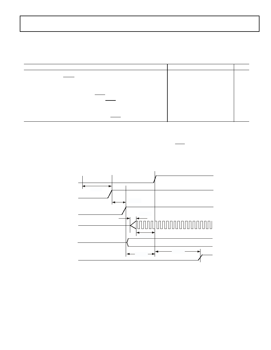
Power-Up Sequencing
The timing requirements for processor startup are given in
Table 11
.
Table 11. Power Up Sequencing Timing Requirements (Processor Startup)
Parameter
Min
Max
Unit
Timing Requirements
t
RSTVDD
RESET Low Before V
DDINT
/V
DDEXT
On
0
ns
t
IVDDEVDD
V
DDINT
on Before V
DDEXT
50
200
ms
t
CLKVDD
1
CLKIN Valid After V
DDINT
/V
DDEXT
Valid
0
200
ms
t
CLKRST
CLKIN Valid Before RESET Deasserted
10
2
s
t
PLLRST
PLL Control Setup Before RESET Deasserted
20
3
s
Switching Characteristic
t
CORERST
Core Reset Deasserted After RESET Deasserted
4096t
CK
+ 2 t
CCLK
4,
5
1
Valid V
DDINT
/V
DDEXT
assumes that the supplies are fully ramped to their 1.2 and 3.3 volt rails. Voltage ramp rates can vary from microseconds to hundreds of milliseconds
depending on the design of the power supply subsystem.
2
Assumes a stable CLKIN signal, after meeting worst-case startup timing of crystal oscillators. Refer to your crystal oscillator manufacturer's datasheet for startup time.
Assume a 25 ms maximum oscillator startup time if using the XTAL pin and internal oscillator circuit in conjunction with an external crystal.
3
Based on CLKIN cycles
4
Applies after the power-up sequence is complete. Subsequent resets require a minimum of four CLKIN cycles for RESET to be held low in order to properly initialize and
propagate default states at all I/O pins.
5
The 4096 cycle count depends on t
SRST
specification in
Table 13
. If setup time is not met, one additional CLKIN cycle may be added to the core reset time, resulting in
4097 cycles maximum.
Figure 3. Power-Up Sequencing
CLKIN
RESET
t
RSTVDD
RSTOUT
VDDEXT
VDDINT
t
PLLRST
t
CLKRST
t
CLKVDD
t
IVDDEVDD
CLK_CFG1-0
t
CORERST
Rev. PrB
|
Page 20 of 42
|
December 2005
ADSP-21375
Preliminary Technical Data
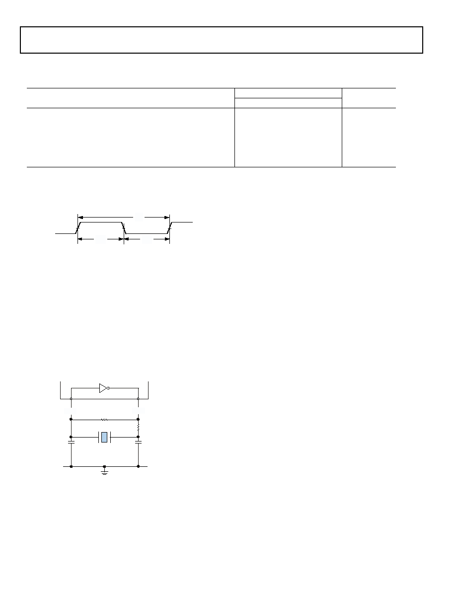
Clock Input
Clock Signals
The ADSP-21375 can use an external clock or a crystal. See the
CLKIN pin description in
Table 5
. The programmer can config-
ure the ADSP-21375 to use its internal clock generator by
connecting the necessary components to CLKIN and XTAL.
Figure 5
shows the component connections used for a crystal
operating in fundamental mode. Note that the clock rate is
achieved using a 16.67 MHz crystal and a PLL multiplier ratio
16:1 (CCLK:CLKIN achieves a clock speed of 266 MHz). To
achieve the full core clock rate, programs need to configure the
multiplier bits in the PMCTL register.
Table 12. Clock Input
Parameter
266 MHz
Unit
Min
Max
Timing Requirements
t
CK
CLKIN Period
22.5
1
1
Applies only for CLKCFG10 = 00 and default values for PLL control bits in PMCTL.
320
2
2
Applies only for CLKCFG10 = 01 and default values for PLL control bits in PMCTL.
ns
t
CKL
CLKIN Width Low
9
1
150
2
ns
t
CKH
CLKIN Width High
9
1
150
2
ns
t
CKRF
CLKIN Rise/Fall (0.4V2.0V)
TBD
ns
t
CCLK
3
3
Any changes to PLL control bits in the PMCTL register must meet core clock timing specification t
CCLK
.
CCLK Period
3.75
1
10
ns
Figure 4. Clock Input
CLKIN
t
CK
t
CKH
t
CKL
Figure 5. 266 MHz Operation (Fundamental Mode Crystal)
C1
22pF
Y1
R1
1M *
XTAL
CLKIN
C2
22pF
16.67 MHz
R2
47 *
R2 SHOULD BE CHOSEN TO LIMIT CRYSTAL
DRIVE POWER. REFER TO CRYSTAL
MANUFACTURER'S SPECIFICATIONS
*TYPICAL VALUES
ADSP-2137X
ADSP-21375
Preliminary Technical Data
Rev. PrB
|
Page 21 of 42
|
December 2005
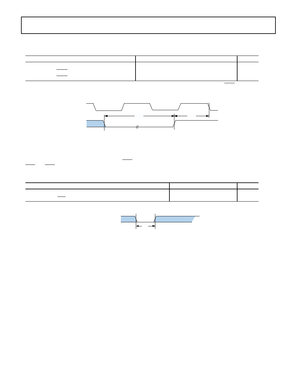
Reset
Interrupts
The following timing specification applies to the FLAG0,
FLAG1, and FLAG2 pins when they are configured as IRQ0,
IRQ1, and IRQ2 interrupts.
Table 13. Reset
Parameter
Min
Max
Unit
Timing Requirements
t
WRST
1
RESET Pulse Width Low
4t
CK
ns
t
SRST
RESET Setup Before CLKIN Low
8
ns
1
Applies after the power-up sequence is complete. At power-up, the processor's internal phase-locked loop requires no more than 100 s while RESET is low, assuming
stable VDD and CLKIN (not including start-up time of external clock oscillator).
Figure 6. Reset
CLKIN
RESET
t
WRST
t
SRST
Table 14. Interrupts
Parameter
Min
Max
Unit
Timing Requirement
t
IPW
IRQx Pulse Width
2 × t
PCLK
+2
ns
Figure 7. Interrupts
DAI_P20-1
DPI_14-1
FLAG2-0
(IRQ2
-
0)
t
IPW
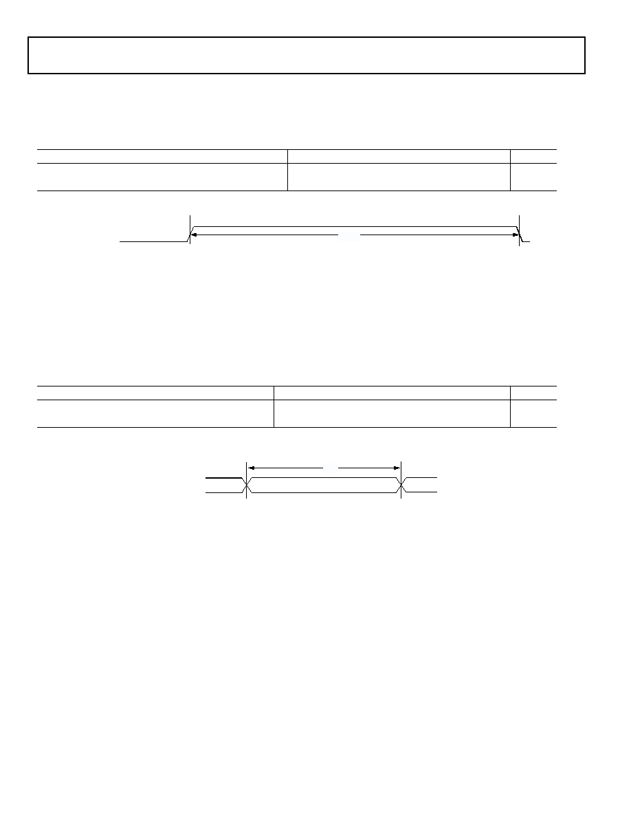
Rev. PrB
|
Page 22 of 42
|
December 2005
ADSP-21375
Preliminary Technical Data
Core Timer
The following timing specification applies to FLAG3 when it is
configured as the core timer (CTIMER).
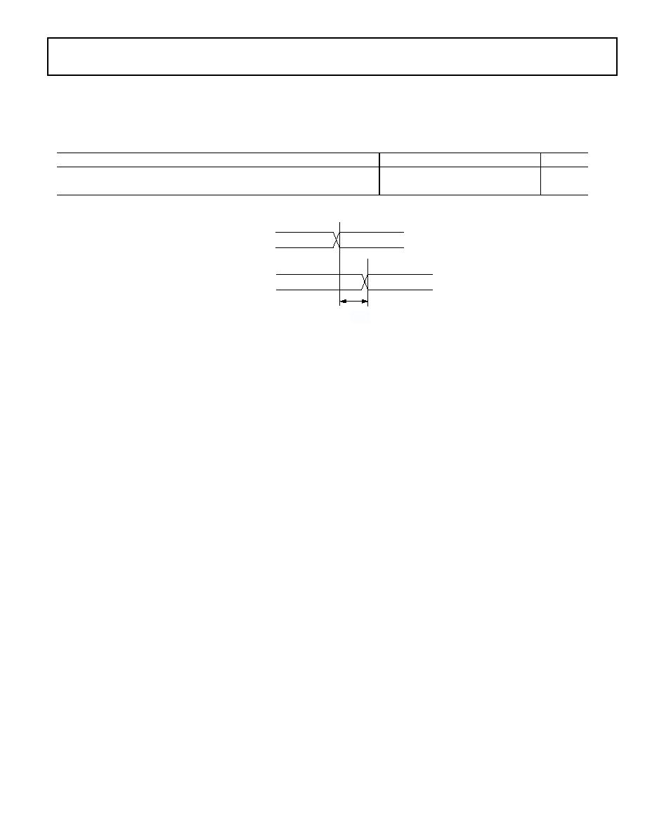
Timer WDTH_CAP Timing
The following timing specification applies to timer0, and
timer1, and in WDTH_CAP (pulse width count and capture)
mode. Timer signals are routed to the DPI_P141 pins through
the SRU. Therefore, the timing specification provided below is
valid at the DPI_P141 pins.
Table 15. Core Timer
Parameter
Min
Max Unit
Switching Characteristic
t
WCTIM
CTIMER Pulse width
4 × t
PCLK
1
ns
Figure 8. Core Timer
FLAG3
(CTIMER)
t
W CTIM
Table 16. Timer Width Capture Timing
Parameter
Min
Max Unit
Timing Requirement
t
PWI
Timer Pulse Width
2 t
PCLK
2(2
31
1) t
PCLK
ns
Figure 9. Timer Width Capture Timing
DPI_14
-
1
(TIMER2-0)
t
PWI
ADSP-21375
Preliminary Technical Data
Rev. PrB
|
Page 23 of 42
|
December 2005
Pin to Pin Direct Routing (DAI and DPI)
For direct pin connections only (for example DAI_PB01_I to
DAI_PB02_O).
Table 17. DAI Pin to Pin Routing
Parameter
Min
Max
Unit
Timing Requirement
t
DPIO
Delay DAI/DPI Pin Input Valid to DAI Output Valid
1.5
10
ns
Figure 10. DAI Pin to Pin Direct Routing
DAI_Pn
DPI_Pn
t
DPIO
DAI_pm
DPI_Pm
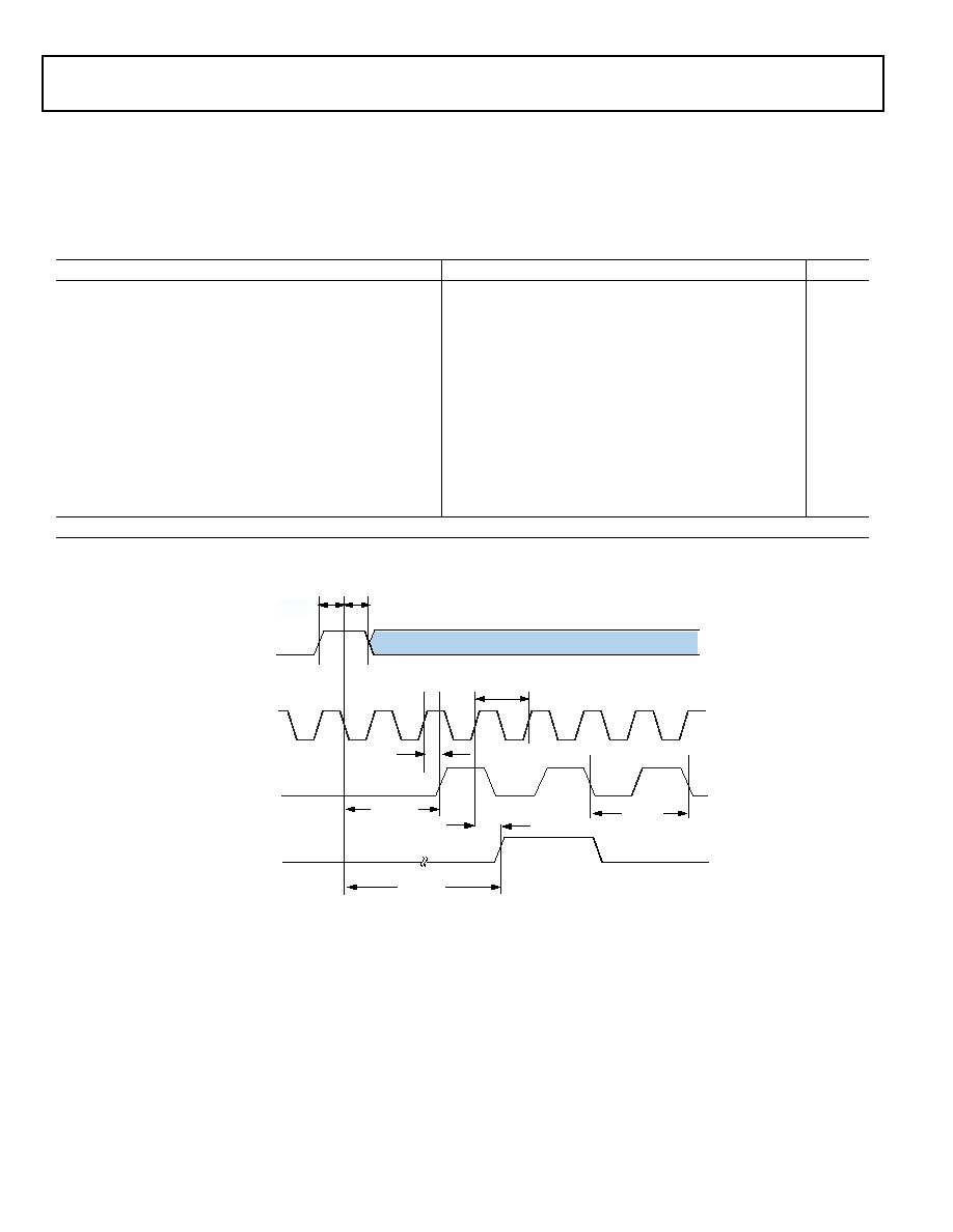
Rev. PrB
|
Page 24 of 42
|
December 2005
ADSP-21375
Preliminary Technical Data
Precision Clock Generator (Direct Pin Routing)
This timing is only valid when the SRU is configured such that
the precision clock generator (PCG) takes its inputs directly
from the DAI pins (via pin buffers) and sends its outputs
directly to the DAI pins. For the other cases, where the PCG's
inputs and outputs are not directly routed to/from DAI pins (via
pin buffers) there is no timing data available. All timing param-
eters and switching characteristics apply to external DAI pins
(DAI_P01 DAI_P20).
Table 18. Precision Clock Generator (Direct Pin Routing)
Parameter
Min
Max
Unit
Timing Requirements
t
PCGIW
Input Clock Period
24
ns
t
STRIG
PCG Trigger Setup Before Falling Edge of PCG Input
Clock
2
ns
t
HTRIG
PCG Trigger Hold After Falling Edge of PCG Input
Clock
2
ns
Switching Characteristics
t
DPCGIO
PCG Output Clock and Frame Sync Active Edge Delay
After PCG Input Clock
2.5
10
ns
t
DTRIGCLK
PCG Output Clock Delay After PCG Trigger
2.5 + ((2.5 + D) × t
PCGIW
)
10 + ((2.5 + D) × t
PCGIW
)
ns
t
DTRIGFS
PCG Frame Sync Delay After PCG Trigger
2.5 + ((2.5 + D PH) × t
PCGIW
)
10 + ((2.5 + D PH) × t
PCGIW
)
ns
t
PCGOW
Output Clock Period
2 × t
PCGIW
1
ns
D = FSxDIV, PH = FSxPHASE.
1
Normal mode of operation.
Figure 11. Precision Clock Generator (Direct Pin Routing)
DAI_Pn
DPI_Pn
PCG_TRIGx_I
t
STRIG
DAI_Pm
DPI_Pm
PCG_EXTx_I
(CLKIN)
DAI_Py
DPI_Py
PCG_CLKx_O
DAI_Pz
DPI_Pz
PCG_FSx_O
t
HTRIG
t
DPCGIO
t
DTRIGFS
t
PCGIW
t
PCGOW
t
DTRIGCLK
t
DPCGIO
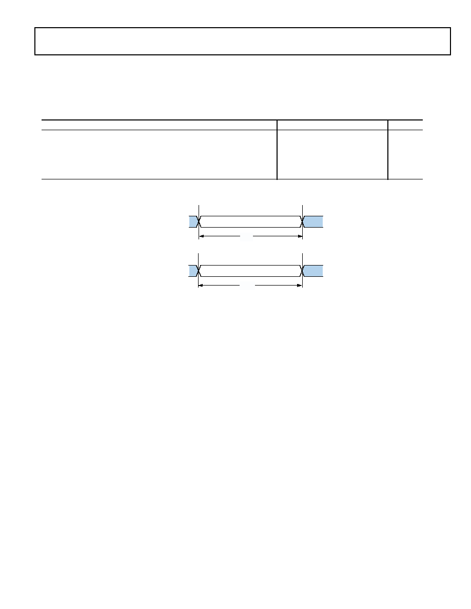
ADSP-21375
Preliminary Technical Data
Rev. PrB
|
Page 25 of 42
|
December 2005
Flags
The timing specifications provided below apply to the FLAG30
and DPI_P141 pins, and the serial peripheral interface (SPI).
See
Table 5
for more information on flag use.
Table 19. Flags
Parameter
Min
Max Unit
Timing Requirement
t
FIPW
FLAG30 IN Pulse Width
2 × t
PCLK
+ 3
ns
Switching Characteristic
t
FOPW
FLAG30 OUT Pulse Width
2 × t
PCLK
1
ns
Figure 12. Flags
DPI_P14
-
1
(FLAG3
-
0
IN
)
(DATA31
-
0)
t
FIPW
DPI_P14
-
1
(FLAG3
-
0
OUT
)
(DATA31
-
0)
t
FOPW
Rev. PrB
|
Page 26 of 42
|
December 2005
ADSP-21375
Preliminary Technical Data
SDRAM Interface Timing (133 MHz SDCLK)
Table 20. SDRAM Interface Timing
1
1
For F
CCLK
= 133 MHz (SDCK ratio = 1:2).
Parameter
Minimum
Maximum
Unit
Timing Requirement
t
SSDAT
DATA Setup Before SDCLK
0.0
ns
t
HSDAT
DATA Hold After SDCLK
1.0
ns
Switching Characteristic
t
SCLK
SDCLK Period
7.5
ns
t
SCLKH
SDCLK Width High
3.65
ns
t
SCLKL
SDCLK Width Low
3.65
ns
t
DCAD
Command, ADDR, Data Delay After SDCLK
2
2
Command pins include: SDCAS, SDRAS, SDWE, MSx, SDA10, and SDCKE.
4.0
ns
t
HCAD
Command, ADDR, Data Hold After SDCLK
2
1.5
ns
t
DSDAT
Data Disable After SDCLK
5.3
ns
t
ENSDAT
Data Enable After SDCLK
2.6
ns
Figure 13. SDRAM Interface Timing for 133 MHz SDCLK
t
HCAD
t
HCAD
t
DSDAT
t
DCAD
t
SSDAT
t
DCAD
t
ENSDAT
t
HSDAT
t
SCLKL
t
SCLKH
t
SCLK
SDCLK
DATA (IN)
DATA(OUT)
CMND ADDR
(OUT)
NOTE: COMMAND =
S DCAS
,
S DR AS
,
S DWE
,
MS x
, SDA10, SDCKE.
ADSP-21375
Preliminary Technical Data
Rev. PrB
|
Page 27 of 42
|
December 2005
Memory Read Bus Master
Use these specifications for asynchronous interfacing to memo-
ries. Note that timing for ACK, DATA, RD, WR, and strobe
timing parameters only apply to asynchronous access mode.
Table 21. Memory Read Bus Master
Parameter
Min
Max
Unit
Timing Requirements
t
DAD
Address, Selects Delay to Data Valid
1, 2
W+t
SDCLK
5.12
ns
t
DRLD
RD Low to Data Valid
1
W 1.5 + t
SDCLK
ns
t
SDS
Data Setup to RD High
1.79
ns
t
HDRH
Data Hold from RD High
3,
4
0
ns
t
DAAK
ACK Delay from Address, Selects
2, 5
t
SDCLK
9.5 + W
ns
t
DSAK
ACK Delay from RD Low
4
W 7.0
ns
t
HAKC
ACK Hold After RD High
0
ns
Switching Characteristics
t
DRHA
Address Selects Hold After RD High
RH + 0.44
ns
t
DARL
Address Selects to RD Low
2
t
SDCLK
3.3
ns
t
RW
RD Pulsewidth
W 0.5
ns
t
RWR
RD High to WR, RD, Low
HI +t
SDCLK
ns
W = (number of wait states specified in AMICTLx register) × t
SDCLK
.
HI =RHC + IC (RHC = (number of Read Hold Cycles specified in AMICTLx register) x t
SDCLK
IC = (number of Idle Cycles specified in AMICTLx register) x t
SDCLK
).
H = (number of Hold Cycles specified in AMICTLx register) x t
SDCLK
.
1
Data Delay/Setup: System must meet t
DAD
, t
DRLD
, or t
SDS.
2
The falling edge of MSx, is referenced.
3
Note that timing for ACK, DATA, RD, WR, and strobe timing parameters only apply to asynchronous access mode.
4
Data Hold: User must meet t
HDA
or t
HDRH
in asynchronous access mode. See
Test Conditions on Page 39
for the calculation of hold times given capacitive and dc loads.
5
ACK Delay/Setup: User must meet t
DAAK
, or t
DSAK
, for deassertion of ACK (low). For asynchronous assertion of ACK (high) user must meet t
DAAK
or t
DSAK
.
Figure 14. Memory Read Bus Master
ACK
DATA
t
DARL
t
RW
t
DAD
t
DAAK
t
HDRH
t
HDA
t
RWR
t
DRLD
t
DRHA
t
DSA K
t
SDS
ADDRESS
MSx
RD
WR
t
HAKC
Rev. PrB
|
Page 28 of 42
|
December 2005
ADSP-21375
Preliminary Technical Data
Memory Write Bus Master
Use these specifications for asynchronous interfacing to memo-
ries. Note that timing for ACK, DATA, RD, WR, and strobe
timing parameters only apply to asynchronous access mode.
Table 22. Memory Write Bus Master
Parameter
Min
Max
Unit
Timing Requirements
t
DAAK
ACK Delay from Address, Selects
1, 2
t
SDCLK
9.7 + W
ns
t
DSAK
ACK Delay from WR Low
1, 3
W 7.1
ns
t
HAKC
ACK Hold After WR High
1
0
ns
Switching Characteristics
t
DAWH
Address, Selects to WR Deasserted
2
t
SDCLK
3.1+ W
ns
t
DAWL
Address, Selects to WR Low
2
t
SDCLK
2.7
ns
t
WW
WR Pulsewidth
W 0.4
ns
t
DDWH
Data Setup Before WR High
t
SDCLK
2.1+ W
ns
t
DWHA
Address Hold After WR Deasserted
H + 0.3
ns
t
DWHD
Data Hold After WR Deasserted
H + 0.4
ns
t
DATRWH
Data Disable After WR Deasserted
4
t
SDCLK
1.37 + H
t
SDCLK
+ 3.9 + H
ns
t
WWR
WR High to WR, RD Low
t
SDCLK
0.2+ H
ns
t
DDWR
Data Disable Before RD Low
2t
SDCLK
4.11
ns
t
WDE
WR Low to Data Enabled
t
SDCLK
3.5
ns
W = (number of wait states specified in AMICTLx register) × t
SDCLK
.
H = (number of hold cycles specified in AMICTLx register) x t
SDCLK
.
1
ACK Delay/Setup: System must meet t
DAAK
, or t
DSAK
, for deassertion of ACK (low). For asynchronous assertion of ACK (high) user must meet t
DAAK
or t
DSAK
.
2
The falling edge of MSx is referenced.
3
Note that timing for ACK, DATA, RD, WR, and strobe timing parameters only applies to asynchronous access mode.
4
See
Test Conditions on Page 39
for calculation of hold times given capacitive and dc loads.
Figure 15. Memory Write Bus Master
t
DATRWH
ACK
DATA
t
DAWL
t
WW
t
DAAK
t
WWR
t
WDE
t
DDWR
t
DWHA
t
DAWH
t
DSAK
t
DDWH
t
DWHD
t
HAKC
ADDRESS
MSx
WR
RD

ADSP-21375
Preliminary Technical Data
Rev. PrB
|
Page 29 of 42
|
December 2005
Serial Ports
To determine whether communication is possible between two
devices at clock speed n, the following specifications must be
confirmed: 1) frame sync delay and frame sync setup and hold,
2) data delay and data setup and hold, and 3) SCLK width.
Serial port signals (SCLK, FS, data channel A, data channel B)
are routed to the DAI_P201 pins using the SRU. Therefore, the
timing specifications provided below are valid at the
DAI_P201 pins.
Table 23. Serial Ports--External Clock
Parameter
Min
Max Unit
Timing Requirements
t
SFSE
1
FS Setup Before SCLK
(Externally Generated FS in either Transmit or Receive Mode)
2.5
ns
t
HFSE
1
FS Hold After SCLK
(Externally Generated FS in either Transmit or Receive Mode)
2.5
ns
t
SDRE
1
Receive Data Setup Before Receive SCLK
2.5
ns
t
HDRE
1
Receive Data Hold After SCLK
2.5
ns
t
SCLKW
SCLK Width
10
ns
t
SCLK
SCLK Period
20
ns
Switching Characteristics
t
DFSE
2
FS Delay After SCLK
(Internally Generated FS in either Transmit or Receive Mode)
7
ns
t
HOFSE
2
FS Hold After SCLK
(Internally Generated FS in either Transmit or Receive Mode)
2
ns
t
DDTE
2
Transmit Data Delay After Transmit SCLK
7
ns
t
HDTE
2
Transmit Data Hold After Transmit SCLK
2
ns
1
Referenced to sample edge.
2
Referenced to drive edge.
Table 24. Serial Ports--Internal Clock
Parameter
Min
Max Unit
Timing Requirements
t
SFSI
1
FS Setup Before SCLK
(Externally Generated FS in either Transmit or Receive Mode)
7
ns
t
HFSI
1
FS Hold After SCLK
(Externally Generated FS in either Transmit or Receive Mode)
2.5
ns
t
SDRI
1
Receive Data Setup Before SCLK
7
ns
t
HDRI
1
Receive Data Hold After SCLK
2.5
ns
Switching Characteristics
t
DFSI
2
FS Delay After SCLK (Internally Generated FS in Transmit Mode)
3
ns
t
HOFSI
2
FS Hold After SCLK (Internally Generated FS in Transmit Mode)
1.0
ns
t
DFSI
2
FS Delay After SCLK (Internally Generated FS in Receive or Mode)
3
ns
t
HOFSI
2
FS Hold After SCLK (Internally Generated FS in Receive Mode)
1.0
ns
t
DDTI
2
Transmit Data Delay After SCLK
3
ns
t
HDTI
2
Transmit Data Hold After SCLK
1.0
ns
t
SCLKIW
Transmit or Receive SCLK Width
0.5t
SCLK
2
0.5t
SCLK
+ 2
ns
1
Referenced to the sample edge.
2
Referenced to drive edge.
Rev. PrB
|
Page 30 of 42
|
December 2005
ADSP-21375
Preliminary Technical Data
Table 25. Serial Ports--Enable and Three-State
Parameter
Min
Max Unit
Switching Characteristics
t
DDTEN
1
Data Enable from External Transmit SCLK
2
ns
t
DDTTE
1
Data Disable from External Transmit SCLK
7
ns
t
DDTIN
1
Data Enable from Internal Transmit SCLK
1
ns
1
Referenced to drive edge.
Table 26. Serial Ports--External Late Frame Sync
Parameter
Min
Max Unit
Switching Characteristics
t
DDTLFSE
1
Data Delay from Late External Transmit FS or External Receive FS
with MCE = 1, MFD = 0
7
ns
t
DDTENFS
1
Data Enable for MCE = 1, MFD = 0
0.5
ns
1
The t
DDTLFSE
and t
DDTENFS
parameters apply to Left-justified Sample Pair as well as DSP serial mode, and MCE = 1, MFD = 0.
Figure 16. External Late Frame Sync
1
1
This figure reflects changes made to support left-justified sample pair mode.
DRIVE
SAMPLE
DRIVE
DAI_P20
-
1
(SCLK)
DAI_P20
-
1
(FS)
DAI_P20
-
1
(DATA CHANNEL A/B)
DRIVE
SAMPLE
DRIVE
LATE EXTERNAL TRANSMIT FS
EXTERNAL RECEIVE FS WITH MCE = 1, MFD = 0
1ST BIT
2ND BIT
DAI_P20
-
1
(SCLK)
DAI_P20
-
1
(FS)
1ST BIT
2ND BIT
t
HFSE/I
t
SFSE/I
t
DDTE/I
t
DDTENFS
t
DDTLFSE
t
HDTE/I
t
SFSE/I
t
DDTE/I
t
DDTENFS
t
DDTLFSE
t
HDTE/I
DAI_P20
-
1
(DATA CHANNEL A/B)
NOTE: SERIAL PORT SIGNALS (SCLK, FS,
DATA CHANNEL A/B
) ARE ROUTED TO THE DAI_P20
-
1 PINS
USING THE SRU. THE TIMING SPECIFICATIONS PROVIDED HERE ARE VALID AT THE DAI_P20
-
1 PINS.
t
HFSE/I
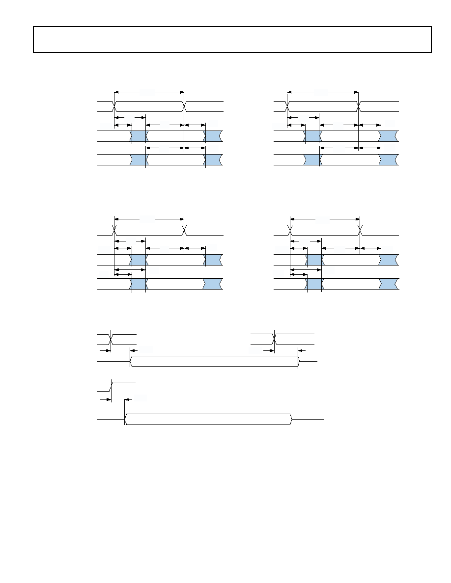
ADSP-21375
Preliminary Technical Data
Rev. PrB
|
Page 31 of 42
|
December 2005
Figure 17. Serial Ports
DRIVE EDGE
DAI_P20
-
1
SCLK (INT)
DRIVE EDGE
DRIVE EDGE
SCLK
DAI_P20
-
1
SCLK (EXT)
t
DDTTE
t
DDTEN
t
DDTIN
DAI_P20
-
1
(DATA CHANNEL A/B)
DAI_P20-1
(DATA CHANNEL A/B)
DAI_P20
-
1
(SCLK)
DAI_P20
-
1
(FS)
DRIVE EDGE
SAMPLE EDGE
DATA RECEIVE--INTERNAL CLOCK
DATA RECEIVE--EXTERNAL CLOCK
DRIVE EDGE
SAMPLE EDGE
NOTE: EITHER THE RISING EDGE OR FALLING EDGE OF SCLK (EXTERNAL) OR SCLK (INTERNAL) CAN BE USED AS THE ACTIVE SAMPLING EDGE.
t
SDRI
t
HDRI
t
SFSI
t
HFSI
t
DFSI
t
HOFSI
t
SCLKIW
t
SDRE
t
HDRE
t
SFSE
t
HFSE
t
DFSE
t
SCLKW
t
HOFSE
DAI_P20
-
1
(DATA CHANNEL A/B)
t
DDTI
DRIVE EDGE
SAMPLE EDGE
DATA TRANSMIT--INTERNAL CLOCK
t
SFSI
t
HFSI
t
DFSI
t
HOFSI
t
SCLKIW
t
HDTI
NOTE: EITHER THE RISING EDGE OR FALLING EDGE OF SCLK (EXTERNAL) OR SCLK (INTERNAL) CAN BE USED AS THE ACTIVE SAMPLING EDGE.
t
DDTE
DRIVE EDGE
SAMPLE EDGE
DATA TRANSMIT--EXTERNAL CLOCK
t
SFSE
t
HFSE
t
DFSE
t
HOFSE
t
SCLKW
t
HDTE
DAI_P20
-
1
(SCLK)
DAI_P20
-
1
(FS)
DAI_P20
-
1
(DATA CHANNEL A/B)
DAI_P20
-
1
(SCLK)
DAI_P20
-
1
(FS)
DAI_P20
-
1
(DATA CHANNEL A/B)
DAI_P20
-
1
(SCLK)
DAI_P20
-
1
(FS)
DAI_P20
-
1
(DATA CHANNEL A/B)
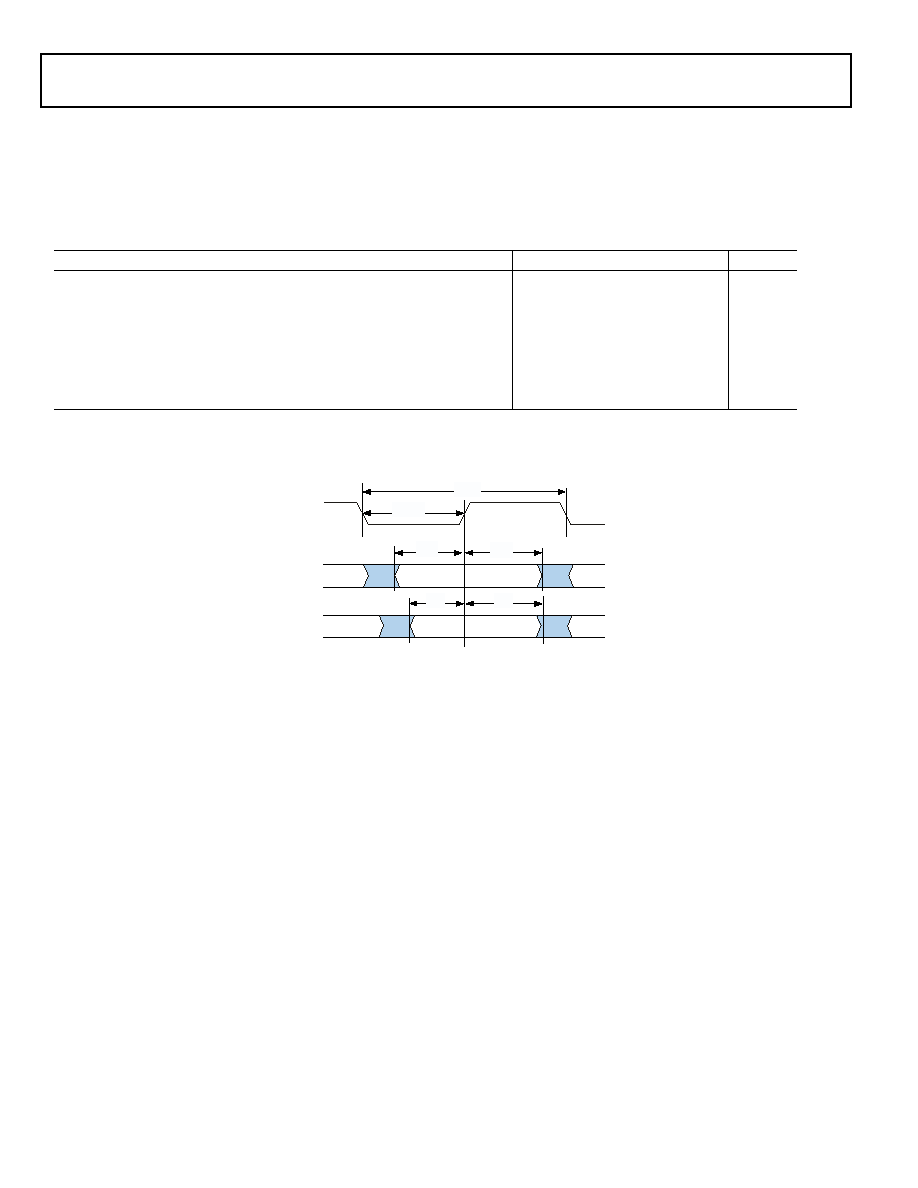
Rev. PrB
|
Page 32 of 42
|
December 2005
ADSP-21375
Preliminary Technical Data
Input Data Port
The timing requirements for the IDP are given in
Table 27
. IDP
signals (SCLK, FS, and SDATA) are routed to the DAI_P201
pins using the SRU. Therefore, the timing specifications pro-
vided below are valid at the DAI_P201 pins.
Table 27. IDP
Parameter
Min
Max Unit
Timing Requirements
t
SISFS
1
FS Setup Before SCLK Rising Edge
2.5
ns
t
SIHFS
1
FS Hold After SCLK Rising Edge
2.5
ns
t
SISD
1
SData Setup Before SCLK Rising Edge
2.5
ns
t
SIHD
1
SData Hold After SCLK Rising Edge
2.5
ns
t
IDPCLKW
Clock Width
9
ns
t
IDPCLK
Clock Period
24
ns
1
DATA, SCLK, FS can come from any of the DAI pins. SCLK and FS can also come via PCG or SPORTs. PCG's input can be either CLKIN or any of the DAI pins.
Figure 18. IDP Master Timing
DAI_P20
-
1
(SCLK)
DAI_P20
-
1
(FS)
SAMPLE EDGE
t
SISFS
t
SIHFS
t
IPDCLK
DAI_P20
-
1
(SDATA)
t
IPDCLKW
t
SISD
t
SIHD
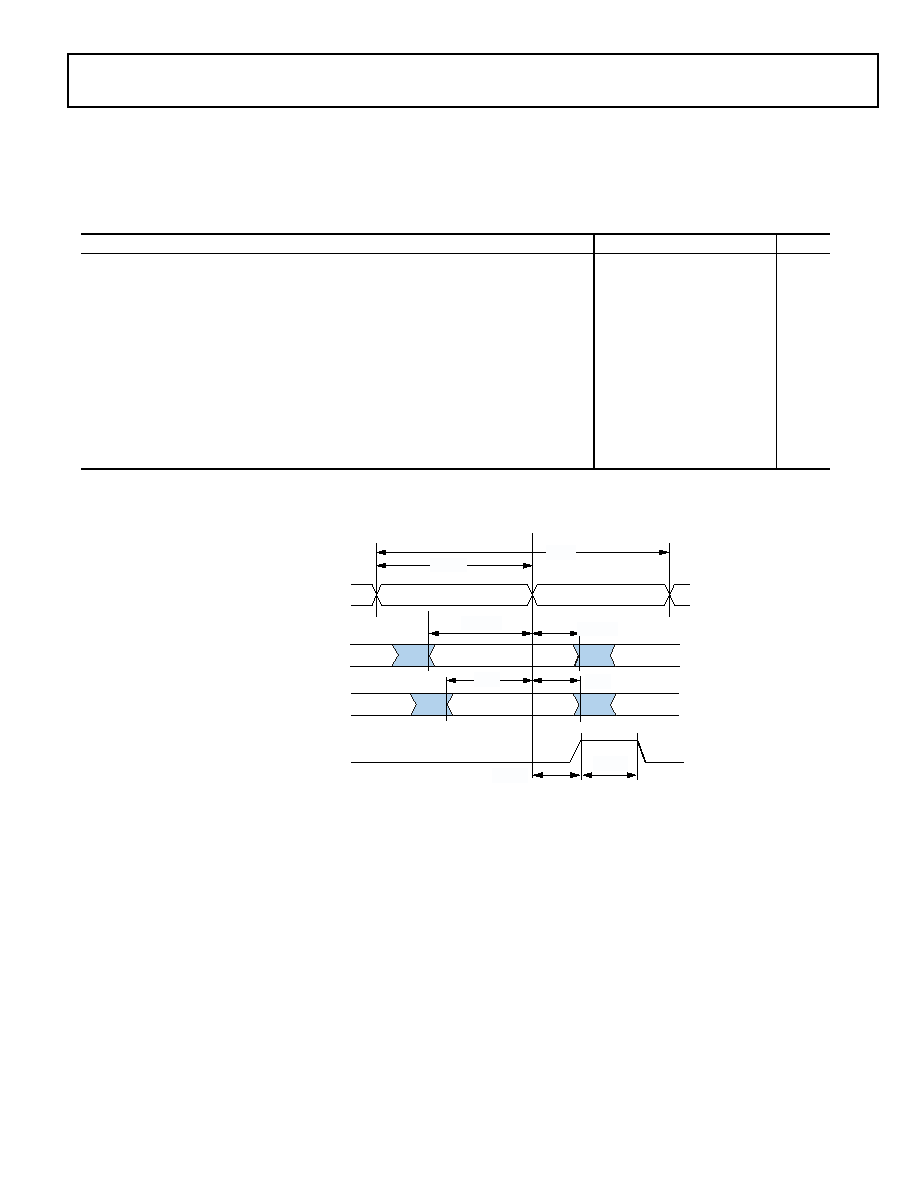
ADSP-21375
Preliminary Technical Data
Rev. PrB
|
Page 33 of 42
|
December 2005
Parallel Data Acquisition Port (PDAP)
The timing requirements for the PDAP are provided in
Table 28
. PDAP is the parallel mode operation of channel 0 of
the IDP. Note that the most significant 16 bits of external PDAP
data can be provided through the DATA3116 pins. The
remaining 4 bits can only be sourced through DAI_P41. The
timing below is valid at the DATA161 pins.
Table 28. Parallel Data Acquisition Port (PDAP)
Parameter
Min
Max
Unit
Timing Requirements
t
SPCLKEN
1
PDAP_CLKEN Setup Before PDAP_CLK Sample Edge
2.5
ns
t
HPCLKEN
1
PDAP_CLKEN Hold After PDAP_CLK Sample Edge
2.5
ns
t
PDSD
1
PDAP_DAT Setup Before SCLK PDAP_CLK Sample Edge
2.5
ns
t
PDHD
1
PDAP_DAT Hold After SCLK PDAP_CLK Sample Edge
2.5
ns
t
PDCLKW
Clock Width
7
ns
t
PDCLK
Clock Period
24
ns
Switching Characteristics
t
PDHLDD
Delay of PDAP Strobe After Last PDAP_CLK Capture Edge for a Word
2 × t
PCLK
1
ns
t
PDSTRB
PDAP Strobe Pulse Width
2 × t
PCLK
1
ns
1
Source pins of DATA are ADDR70, DATA70, or DAI pins. Source pins for SCLK and FS are: 1) DAI pins, 2) CLKIN through PCG, or 3) DAI pins through PCG.
Figure 19. PDAP Timing
DAI_P20
-
1
(PDAP_CLK)
SAMPLE EDGE
t
PDSD
t
PDHD
t
SPCLKEN
t
HPCLKEN
t
PDCLKW
DATA
DAI_P20
-
1
(PDAP_CLKEN)
t
PDSTRB
t
PDHLDD
DAI_P20
-
1
(PDAP_STROBE)
t
PDCLK
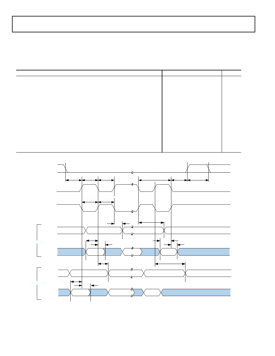
Rev. PrB
|
Page 34 of 42
|
December 2005
ADSP-21375
Preliminary Technical Data
SPI Interface--Master
The ADSP-21375 contains two SPI ports. The primary has dedi-
cated pins and the secondary is available through the DPI. The
timing provided in
Table 29
and
Table 30
applies to both.
Table 29. SPI Interface Protocol -- Master Switching and Timing Specifications
Parameter
Min
Max Unit
Timing Requirements
t
SSPIDM
Data Input Valid To SPICLK Edge (Data Input Set-up Time)
8
ns
t
HSPIDM
SPICLK Last Sampling Edge To Data Input Not Valid
2
ns
Switching Characteristics
t
SPICLKM
Serial Clock Cycle
8 × t
PCLK
ns
t
SPICHM
Serial Clock High Period
4 × t
PCLK
ns
t
SPICLM
Serial Clock Low Period
4 × t
PCLK
2
ns
t
DDSPIDM
SPICLK Edge to Data Out Valid (Data Out Delay Time)
0
t
HDSPIDM
SPICLK Edge to Data Out Not Valid (Data Out Hold Time)
2
ns
t
SDSCIM
FLAG30IN (SPI device select) Low to First SPICLK Edge
4 × t
PCLK
2
ns
t
HDSM
Last SPICLK Edge to FLAG30IN High
4 × t
PCLK
1
ns
t
SPITDM
Sequential Transfer Delay
4 × t
PCLK
1
ns
Figure 20. SPI Master Timing
LSB
VALID
MSB
VALID
t
SS PI DM
t
HS PI DM
t
HDSPIDM
LSB
MSB
t
HSPI DM
t
D DSP I DM
MOSI
(OUTPUT)
MISO
(INPUT)
FLAG3
-
0
(OUTPUT)
SPICLK
(CP = 0)
(OUTPUT)
SPICLK
(CP = 1)
(OUTPUT)
t
SPI CHM
t
SPI CL M
t
SPI CL M
t
SPI CL KM
t
SPI CHM
t
HDSM
t
SPI T DM
t
HDS PI DM
LSB
VALID
LSB
MSB
MSB
VALID
t
HSPI DM
t
DDS PI DM
MOSI
(OUTPUT)
MISO
(INPUT)
t
SS PI DM
CPHASE = 1
CPHASE = 0
t
S DSCI M
t
SSPI DM
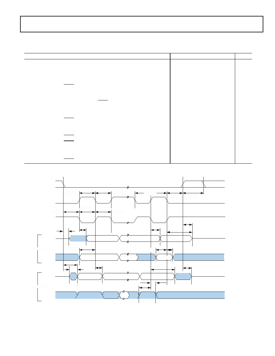
ADSP-21375
Preliminary Technical Data
Rev. PrB
|
Page 35 of 42
|
December 2005
SPI Interface--Slave
Table 30. SPI Interface Protocol --Slave Switching and Timing Specifications
Parameter
Min
Max Unit
Timing Requirements
t
SPICLKS
Serial Clock Cycle
4 × t
PCLK
ns
t
SPICHS
Serial Clock High Period
2 × t
PCLK
ns
t
SPICLS
Serial Clock Low Period
2 × t
PCLK
2
ns
t
SDSCO
SPIDS Assertion to First SPICLK Edge
CPHASE = 0
CPHASE = 1
2 × t
PCLK
2 × t
PCLK
ns
t
HDS
Last SPICLK Edge to SPIDS Not Asserted, CPHASE = 0
2 × t
PCLK
ns
t
SSPIDS
Data Input Valid to SPICLK edge (Data Input Set-up Time)
2
ns
t
HSPIDS
SPICLK Last Sampling Edge to Data Input Not Valid
2
ns
t
SDPPW
SPIDS Deassertion Pulse Width (CPHASE=0)
2 × t
PCLK
ns
Switching Characteristics
t
DSOE
SPIDS Assertion to Data Out Active
0
4
ns
t
DSDHI
SPIDS Deassertion to Data High Impedance
0
4
ns
t
DDSPIDS
SPICLK Edge to Data Out Valid (Data Out Delay Time)
9.4
ns
t
HDSPIDS
SPICLK Edge to Data Out Not Valid (Data Out Hold Time)
2 × t
PCLK
ns
t
DSOV
SPIDS Assertion to Data Out Valid (CPHASE=0)
5 × t
PCLK
ns
Figure 21. SPI Slave Timing
t
H S P I D S
t
D D S P I D S
t
D S D H I
LSB
MSB
MSB VALID
t
D S O E
t
D D S P I D S
t
H D S P I D S
MISO
(OUTPUT)
MOSI
(INPUT)
t
S S P I D S
SPIDS
(INPUT)
SPICLK
(CP = 0)
(INPUT)
SPICLK
(CP = 1)
(INPUT)
t
S D S C O
t
S P IC H S
t
S P I C L S
t
S P I C L S
t
S P I C L K S
t
H D S
t
S P I C H S
t
S S P I D S
t
H S P I D S
t
D S D H I
LSB VALID
MSB
MSB VALID
t
D S O E
t
D D S P I D S
MISO
(OUTPUT)
MOSI
(INPUT)
t
S S P I D S
LSB VALID
LSB
CPHASE = 1
CPHASE = 0
t
S D P P W
t
D S O V
t
H D S P I D S
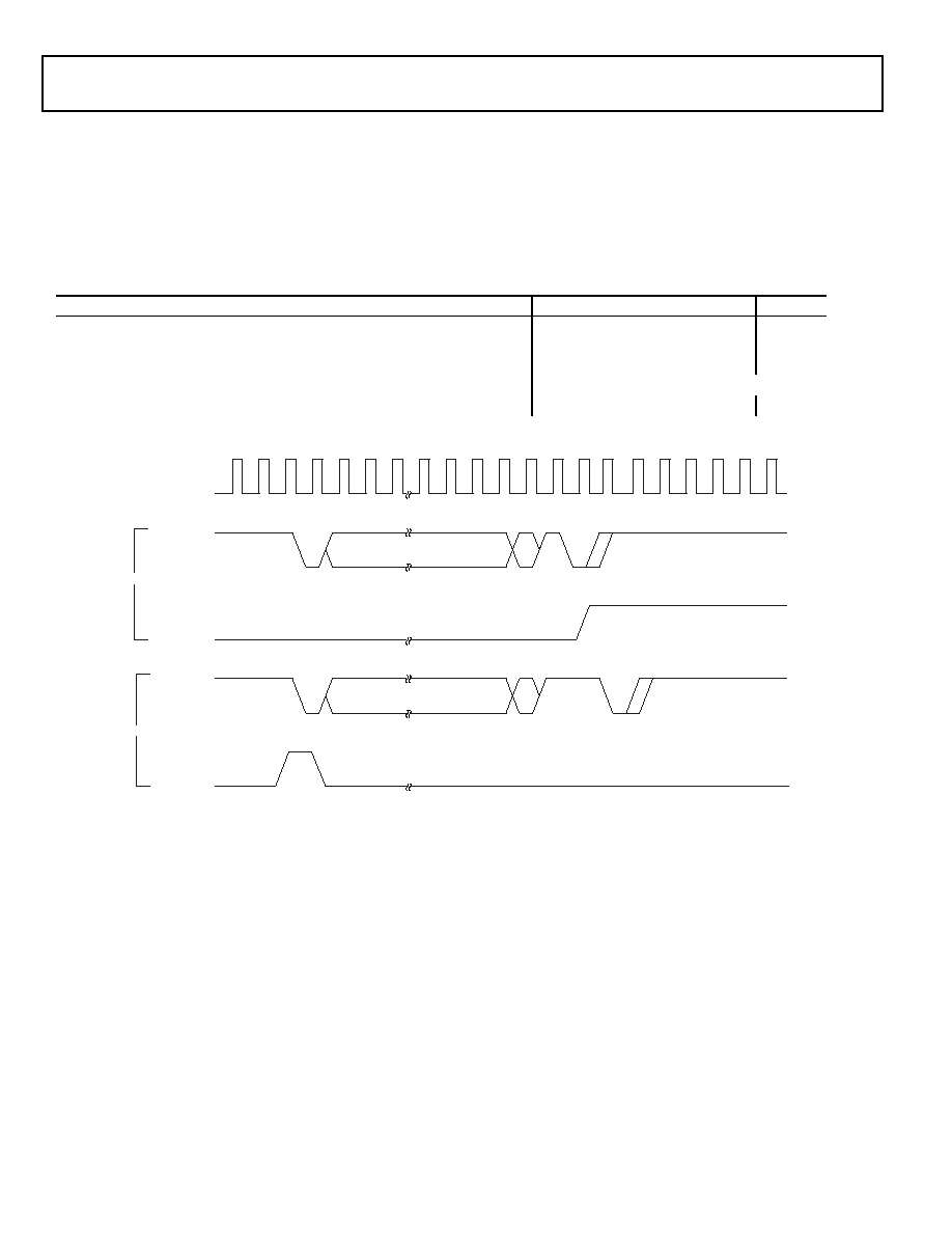
Rev. PrB
|
Page 36 of 42
|
December 2005
ADSP-21375
Preliminary Technical Data
Universal Asynchronous Receiver-Transmitter
(UART) Port--Receive and Transmit Timing
Figure 22
describes UART port receive and transmit operations.
The maximum baud rate is SCLK/16. As shown in
Figure 22
there is some latency between the generation of internal UART
interrupts and the external data operations. These latencies are
negligible at the data transmission rates for the UART.
Table 31. UART Port
Parameter
Min
Max Unit
Timing Requirement
t
RXD
Incoming Data Pulse Width
95
ns
Switching Characteristic
t
RXD
Incoming Data Pulse Width
95
ns
Figure 22. UART Port--Receive and Transmit Timing
DPI_P14
-
1
[RXD]
DATA(5
-
8)
INTERNAL
UART RECEIVE
INTERRUPT
UART RECEIVE BIT SET BY DATA STOP;
CLEARED BY FIFO READ
DPI_P14
-
1
[CLKOUT]
(SAMPLE CLOCK)
DPI_P14
-
1
[TXD]
DATA(5
-
8)
STOP(1
-
2)
INTERNAL
UART TRANSMIT
INTERRUPT
UART TRANSMIT BIT SET BY PROGRAM;
CLEARED BY WRITE TO TRANSMIT
START
STOP
TRANSMIT
RECEIVE
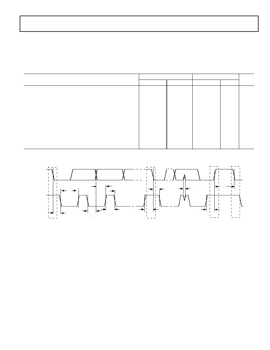
ADSP-21375
Preliminary Technical Data
Rev. PrB
|
Page 37 of 42
|
December 2005
TWI Controller Timing
Table 32
and
Figure 23
provide timing information for the TWI
interface. Input Signals (SCL, SDA) are routed to the
DPI_P141 pins using the SRU. Therefore, the timing specifica-
tions provided below are valid at the DPI_P141 pins.
Table 32. Characteristics of the SDA and SCL Bus Lines for F/S-Mode TWI Bus Devices
1
Parameter
Standard-mode Fast-mode
Unit
Min
Max
Min
Max
f
SCL
SCL
Clock
Frequency
0 100
0 400
kHz
t
HDSTA
Hold Time (repeated) START Condition. After this
Period, the First Clock Pulse is Generated.
4.0
0.6
s
t
LOW
LOW Period of the SCL Clock
4.7
1.3
s
t
HIGH
HIGH period of the SCL Clock
4.0
0.6
s
t
SUSTA
Set-up time for a repeated START condition
4.7
0.6
s
t
HDDAT
Data Hold Time for TWI-bus Devices
0
0
s
t
SUDAT
Data Set-up Time
250
100
ns
t
SUSTO
Set-up Time for STOP Condition
4.0
0.6
s
t
BUF
Bus Free Time Between a STOP and START Condition 4.7
1.3
s
t
SP
Pulse Width of Spikes Suppressed By the Input Filter n/a
n/a
0
50
ns
1
All values referred to V
IH
MIN
and V
IL
MAX
levels.
For more information, see Electrical Characteristics on page 16.
Figure 23. Fast and Standard Mode Timing on the TWI Bus
DPI_P14-1
SDA
DPI_P14-1
SCL
t
LOW
t
H IGH
t
H DS TA
t
H DD A T
t
SU D A T
t
SU STO
S
t
SU S TA
Sr
t
SP
t
H D S TA
P
S
t
B UF
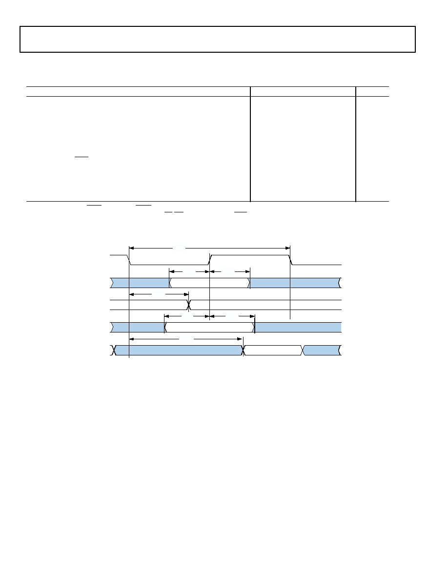
Rev. PrB
|
Page 38 of 42
|
December 2005
ADSP-21375
Preliminary Technical Data
JTAG Test Access Port and Emulation
Table 33. JTAG Test Access Port and Emulation
Parameter
Min
Max Unit
Timing Requirements
t
TCK
TCK Period
t
CK
ns
t
STAP
TDI, TMS Setup Before TCK High
5
ns
t
HTAP
TDI, TMS Hold After TCK High
6
ns
t
SSYS
1
System Inputs Setup Before TCK High
7
ns
t
HSYS
1
System Inputs Hold After TCK High
18
ns
t
TRSTW
TRST Pulse Width
4t
CK
ns
Switching Characteristics
t
DTDO
TDO Delay from TCK Low
7
ns
t
DSYS
2
System Outputs Delay After TCK Low
t
CK
÷ 2 + 7
ns
1
System Inputs = AD150, SPIDS, CLKCFG10, RESET, BOOTCFG10, MISO, MOSI, SPICLK, DAI_Px, and FLAG30.
2
System Outputs = MISO, MOSI, SPICLK, DAI_Px, AD150, RD, WR, FLAG30, CLKOUT, EMU, and ALE.
Figure 24. IEEE 1149.1 JTAG Test Access Port
TCK
TMS
TDI
TDO
SYSTEM
INPUTS
SYSTEM
OUTPUTS
t
STAP
t
TCK
t
HTAP
t
DTDO
t
SSYS
t
HSYS
t
DSYS
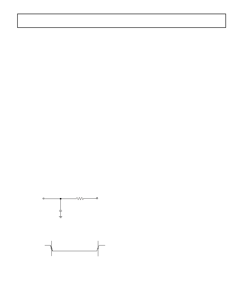
ADSP-21375
Preliminary Technical Data
Rev. PrB
|
Page 39 of 42
|
December 2005
OUTPUT DRIVE CURRENTS
Figure 25
shows typical I-V characteristics for the output driv-
ers of the ADSP-21375. The curves represent the current drive
capability of the output drivers as a function of output voltage.
TEST CONDITIONS
The ac signal specifications (timing parameters) appear
Table 13 on page 21
through
Table 33 on page 38
. These include
output disable time, output enable time, and capacitive loading.
The timing specifications for the SHARC apply for the voltage
reference levels in
Figure 26
.
Timing is measured on signals when they cross the 1.5 V level as
described in
Figure 27
. All delays (in nanoseconds) are mea-
sured between the point that the first signal reaches 1.5 V and
the point that the second signal reaches 1.5 V.
CAPACITIVE LOADING
Output delays and holds are based on standard capacitive loads:
30 pF on all pins (see
Figure 26
).
Figure 30
shows graphically
how output delays and holds vary with load capacitance. The
graphs of
Figure 28
,
Figure 29
, and
Figure 30
may not be linear
outside the ranges shown for Typical Output Delay vs. Load
Capacitance and Typical Output Rise Time (20%-80%, V=Min)
vs. Load Capacitance.
Figure 25. ADSP-21375 Typical Drive
Figure 26. Equivalent Device Loading for AC Measurements
(Includes All Fixtures)
Figure 27. Voltage Reference Levels for AC Measurements
TBD
1.5V
30pF
TO
OUTPUT
PIN
50
INPUT
OR
OUTPUT
1.5V
1.5V
Figure 28. Typical Output Rise/Fall Time (20%-80%,
V
DDEXT
= Max)
Figure 29. Typical Output Rise/Fall Time (20%-80%,
V
DDEXT
=Min)
Figure 30. Typical Output Delay or Hold vs. Load Capacitance
(at Ambient Temperature)
TBD
TBD
TBD

Rev. PrB
|
Page 40 of 42
|
December 2005
ADSP-21375
Preliminary Technical Data
THERMAL CHARACTERISTICS
The ADSP-21375 processor is rated for performance over the
temperature range specified in
Recommended Operating Con-
ditions on Page 16
.
Table 34
airflow measurements comply with JEDEC standards
JESD51-2 and JESD51-6 and the junction-to-board measure-
ment complies with JESD51-8. Test board design complies with
JEDEC standards JESD51-7 (MQFP). The junction-to-case
measurement complies with MIL- STD-883. All measurements
use a 2S2P JEDEC test board.
To determine the junction temperature of the device while on
the application PCB, use:
where:
T
J
= Junction temperature °C
T
CASE
= Case temperature (°C) measured at the top center of
the package
JT
= Junction-to-top (of package) characterization parameter
is the Typical value from
Table 34
.
P
D
= Power dissipation (see EE Note #TBD)
Values of
JA
are provided for package comparison and PCB
design considerations.
JA
can be used for a first order approxi-
mation of T
J
by the equation:
where:
T
A
= ambient temperature °C
Values of
JC
are provided for package comparison and PCB
design considerations when an external heatsink is required.
Values of
JB
are provided for package comparison and PCB
design considerations. Note that the thermal characteristics val-
ues provided in
Table 34
are modeled values.
Table 34. Thermal Characteristics for 208-Lead MQFP
Parameter
Condition
Typical
Unit
JA
Airflow = 0 m/s
TBD
°C/W
JMA
Airflow = 1 m/s
TBD
°C/W
JMA
Airflow = 2 m/s
TBD
°C/W
JC
TBD
°C/W
JT
Airflow = 0 m/s
TBD
°C/W
JMT
Airflow = 1 m/s
TBD
°C/W
JMT
Airflow = 2 m/s
TBD
°C/W
T
J
T
CASE
JT
P
D
×
(
)
+
=
T
J
T
A
JA
P
D
×
(
)
+
=
ADSP-21375
Preliminary Technical Data
Rev. PrB
|
Page 41 of 42
|
December 2005
208-LEAD MQFP PINOUT
Table 35. 208-Lead MQFP Pin Assignment (Numerically by Lead Number)
Pin No.
Signal
Pin No.
Signal
Pin No.
Signal
Pin No.
Signal
1
VDD
53
VDD
105
VDD
157
VDD
2
NC
54
GND
106
GND
158
VDD
3
NC
55
IOVDD
107
IOVDD
159
GND
4
GND
56
ADDR0
108
SDCAS
160
VDD
5
IOVDD
57
ADDR2
109
SDRAS
161
VDD
6
NC
58
ADDR1
110
SDCKE
162
VDD
7
NC
59
ADDR4
111
SDWE
163
TDI
8
NC
60
ADDR3
112
WR
164
TRST
9
NC
61
ADDR5
113
SDA10
165
TCK
10
GND
62
GND
114
GND
166
GND
11
VDD
63
VDD
115
IOVDD
167
VDD
12
NC
64
GND
116
SDCLKO
168
TMS
13
NC
65
IOVDD
117
GND
169
CLK_CFG0
14
NC
66
ADDR6
118
VDD
170
BOOTCFG0
15
NC
67
ADDR7
119
RD
171
CLK_CFG1
16
NC
68
ADDR8
120
ACK
172
EMU
17
NC
69
ADDR9
121
FLAG3
173
BOOTCFG1
18
NC
70
ADDR10
122
FLAG2
174
TDO
19
NC
71
GND
123
FLAG1
175
DAI4
20
NC
72
VDD
124
FLAG0
176
DAI2
21
NC
73
GND
125
DAI20
177
DAI3
22
VDD
74
IOVDD
126
GND
178
DAI1
23
GND
75
ADDR11
127
VDD
179
IOVDD
24
VDD
76
ADDR12
128
GND
180
GND
25
GND
77
ADDR13
129
IOVDD
181
VDD
26
NC
78
GND
130
DAI19
182
GND
27
DATA15
79
VDD
131
DAI18
183
DPI14
28
DATA14
80
NC
132
DAI17
184
DPI13
29
DATA13
81
NC
133
DAI16
185
DPI12
30
DATA12
82
GND
134
DAI15
186
DPI11
31
IOVDD
83
CLKIN
135
DAI14
187
DPI10
32
GND
84
XTAL
136
DAI13
188
DPI9
33
VDD
85
IOVDD
137
DAI12
189
DPI8
34
GND
86
GND
138
VDD
190
DPI7
35
DATA11
87
VDD
139
IOVDD
191
IOVDD
36
DATA10
88
ADDR14
140
GND
192
GND
37
DATA9
89
GND
141
VDD
193
VDD
38
DATA8
90
IOVDD
142
GND
194
GND
39
DATA7
91
ADDR15
143
DAI11
195
DPI6
40
DATA6
92
ADDR16
144
DAI10
196
DPI5
41
IOVDD
93
ADDR17
145
DAI8
197
DPI4
42
GND
94
ADDR18
146
DAI9
198
DPI3
43
VDD
95
GND
147
DAI6
199
DPI1
44
DATA4
96
IOVDD
148
DAI7
200
DPI2
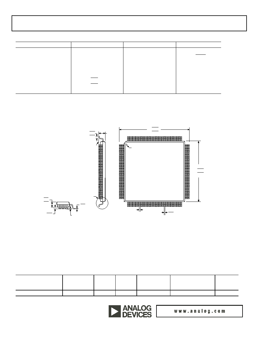
Rev. PrB
|
Page 42 of 42
|
December 2005
ADSP-21375
Preliminary Technical Data
© 2005 Analog Devices, Inc. All rights reserved. Trademarks and
registered trademarks are the property of their respective owners.
PACKAGE DIMENSIONS
The ADSP-21375 is available in a 208-lead Pb-free MQFP package.
ORDERING GUIDE
45
DATA5
97
ADDR19
149
DAI5
201
CLKOUT
46
DATA2
98
ADDR20
150
IOVDD
202
RESET
47
DATA3
99
ADDR21
151
GND
203
IOVDD
48
DATA0
100
ADDR23
152
VDD
204
GND
49
DATA1
101
ADDR22
153
GND
205
NC
50
IOVDD
102
MS1
154
VDD
206
NC
51
GND
103
MS0
155
GND
207
NC
52
VDD
104
VDD
156
VDD
208
VDD
Figure 31. 208-Lead MQFP (S-208-2)
Part Number
Ambient
Temperature
Range
On-Chip
SRAM
ROM
Operating Voltage Package Description
Package
Option
ADSP-21375KSZ-ENG
1
1
Z= Pb Free package.
0
°C to +70°C
0.5M bit
2M bit
1.2 INT/3.3 EXT V
208-Lead MQFP, Pb-Free
S-208-2
Table 35. 208-Lead MQFP Pin Assignment (Numerically by Lead Number) (Continued)
Pin No.
Signal
Pin No.
Signal
Pin No.
Signal
Pin No.
Signal
0.20
0.09
3.60
3.40
3.20
0.50
0.25
0.08 MAX
(LEAD COPLANARITY)
VIEW A
ROTATED 90° CCW
1
208
157
156
105
104
53
52
TOP VIEW
(PINS DOWN)
0.50
BSC
28.20
28.00 SQ
27.80
0.27
0.17
(LEAD PITCH)
(LEAD WIDTH)
SEATING
PLANE
4.10
MAX
0.75
0.60
0.45
NOTES:
1. THE ACTUAL POSITION OF EACH LEAD IS WITHIN 0.08 FROM ITS IDEAL
POSITION WHEN MEASURED IN THE LATERAL DIRECTION.
2. CENTER DIMENSIONS ARE TYPICAL UNLESS OTHERWISE NOTED.
3. DIMENSIONS ARE IN MILLIMETERS AND COMPLY WITH JEDEC
STANDARD MS-029, FA-1.
30.85
30.60 SQ
30.35
VIEW A
PIN 1 INDICATOR
PR05842-0-12/05(PrB)
Document Outline