ADSP-216x Data Sheet
REV. 0
Information furnished by Analog Devices is believed to be accurate and
reliable. However, no responsibility is assumed by Analog Devices for its
use, nor for any infringements of patents or other rights of third parties
which may result from its use. No license is granted by implication or
otherwise under any patent or patent rights of Analog Devices.
a
ADSP-216x
One Technology Way, P.O. Box 9106, Norwood, MA 02062-9106, U.S.A.
Tel: 781/329-4700
World Wide Web Site: http://www.analog.com
Fax: 781/326-8703
© Analog Devices, Inc., 1999
DSP Microcomputers with ROM
FUNCTIONAL BLOCK DIAGRAM
SERIAL PORTS
SPORT 1
SPORT 0
MEMORY
TIMER
SHIFTER
MAC
ALU
ARITHMETIC UNITS
DAG 2
DAG 1
DATA ADDRESS
GENERATORS
EXTERNAL
DATA
BUS
EXTERNAL
ADDRESS
BUS
PROGRAM
MEMORY
DATA
MEMORY
DATA MEMORY DATA
DATA MEMORY ADDRESS
PROGRAM MEMORY ADDRESS
PROGRAM MEMORY DATA
PROGRAM
SEQUENCER
ADSP-2100 CORE
SUMMARY
16-Bit Fixed-Point DSP Microprocessors with
On-Chip Memory
Enhanced Harvard Architecture for Three-Bus
Performance: Instruction Bus and Dual Data Buses
Independent Computation Units: ALU, Multiplier/
Accumulator and Shifter
Single-Cycle Instruction Execution and Multifunction
Instructions
On-Chip Program Memory ROM and Data Memory RAM
Integrated I/O Peripherals: Serial Ports, Timer
FEATURES
25 MIPS, 40 ns Maximum Instruction Rate (5 V)
Separate On-Chip Buses for Program and Data Memory
Program Memory Stores Both Instructions and Data
(Three-Bus Performance)
Dual Data Address Generators with Modulo and
Bit-Reverse Addressing
Efficient Program Sequencing with Zero-Overhead
Looping: Single-Cycle Loop Setup
Double-Buffered Serial Ports with Companding Hardware,
Automatic Data Buffering and Multichannel Operation
Three Edge- or Level-Sensitive Interrupts
Low Power IDLE Instruction
PLCC and MQFP Packages
GENERAL DESCRIPTION
The ADSP-216x Family processors are single-chip micro-
computers optimized for digital signal processing (DSP)
and other high speed numeric processing applications. The
ADSP-216x processors are all built upon a common core with
ADSP-2100. Each processor combines the core DSP architec-
ture--computation units, data address generators and program
sequencer--with features such as on-chip program ROM and
data memory RAM, a programmable timer and two serial ports.
The ADSP-2165/ADSP-2166 also adds program memory and
power-down mode.
This data sheet describes the following ADSP-216x Family
processors:
ADSP-2161/ADSP-2162/
ADSP-2163/ADSP-2164
Custom ROM-programmed DSPs:
ADSP-2165/ADSP-2166
ROM-programmed ADSP-216x
processors with power-down and
larger on-chip memories (12K Pro-
gram Memory ROM, 1K Program
Memory RAM, 4K Data Memory
RAM)
Fabricated in a high speed, submicron, double-layer metal
CMOS process, the highest-performance ADSP-216x proces-
sors operate at 25 MHz with a 40 ns instruction cycle time.
Every instruction can execute in a single cycle. Fabrication in
CMOS results in low power dissipation.
The ADSP-2100 Family's flexible architecture and compre-
hensive instruction set support a high degree of parallelism.
In one cycle the ADSP-216x can perform all of the following
operations:
·
Generate the next program address
·
Fetch the next instruction
·
Perform one or two data moves
·
Update one or two data address pointers
·
Perform a computation
·
Receive and transmit data via one or two serial ports
Table I shows the features of each ADSP-216x processor.
The ADSP-216x series are memory-variant versions of the
ADSP-2101 and ADSP-2103 that contain factory-programmed
on-chip ROM program memory. These devices offer different
amounts of on-chip memory for program and data storage.
Table I shows the features available in the ADSP-216x series of
custom ROM-coded processors.
The ADSP-216x products eliminate the need for an external
boot EPROM in your system, and can also eliminate the need
for any external program memory by fitting the entire applica-
tion program in on-chip ROM. These devices thus provide an
excellent option for volume applications where board space and
system cost constraints are of critical concern.

REV. 0
ADSP-216x
2
TABLE OF CONTENTS
SUMMARY . . . . . . . . . . . . . . . . . . . . . . . . . . . . . . . . . . . . 1
FEATURES . . . . . . . . . . . . . . . . . . . . . . . . . . . . . . . . . . . . 1
GENERAL DESCRIPTION . . . . . . . . . . . . . . . . . . . . . . . . 1
Development Tools . . . . . . . . . . . . . . . . . . . . . . . . . . . . . . . 3
Additional Information . . . . . . . . . . . . . . . . . . . . . . . . . . . . 3
ARCHITECTURE OVERVIEW . . . . . . . . . . . . . . . . . . . . 3
Serial Ports . . . . . . . . . . . . . . . . . . . . . . . . . . . . . . . . . . . . . . 4
Interrupts . . . . . . . . . . . . . . . . . . . . . . . . . . . . . . . . . . . . . . . . 5
SYSTEM INTERFACE . . . . . . . . . . . . . . . . . . . . . . . . . . . . 5
Clock Signals . . . . . . . . . . . . . . . . . . . . . . . . . . . . . . . . . . . . . 5
Reset . . . . . . . . . . . . . . . . . . . . . . . . . . . . . . . . . . . . . . . . . . . 6
PIN FUNCTION DESCRIPTIONS . . . . . . . . . . . . . . . . . . 6
Program Memory Interface . . . . . . . . . . . . . . . . . . . . . . . . . . 7
Program Memory Maps . . . . . . . . . . . . . . . . . . . . . . . . . . . . . 7
Data Memory Interface . . . . . . . . . . . . . . . . . . . . . . . . . . . . . 8
Data Memory Map . . . . . . . . . . . . . . . . . . . . . . . . . . . . . . . . 8
Bus Interface . . . . . . . . . . . . . . . . . . . . . . . . . . . . . . . . . . . . . 9
POWER-DOWN . . . . . . . . . . . . . . . . . . . . . . . . . . . . . . . . . . 9
Power-Down Control . . . . . . . . . . . . . . . . . . . . . . . . . . . . . . 9
Entering Power-Down . . . . . . . . . . . . . . . . . . . . . . . . . . . . . . 9
Exiting Power-Down . . . . . . . . . . . . . . . . . . . . . . . . . . . . . . 10
Low Power IDLE Instruction . . . . . . . . . . . . . . . . . . . . . . . 10
ADSP-216x Prototyping . . . . . . . . . . . . . . . . . . . . . . . . . . . 10
Ordering Procedure for ADSP-216x ROM Processors . . . . 10
Instruction Set . . . . . . . . . . . . . . . . . . . . . . . . . . . . . . . . . . . 11
SPECIFICATIONSRECOMMENDED OPERATING
CONDITIONS
(ADSP-2161/ADSP-2163/ADSP-2165) . . . . . . . . . . . . . . 13
ELECTRICAL CHARACTERISTICS . . . . . . . . . . . . . . . . 13
ABSOLUTE MAXIMUM RATINGS . . . . . . . . . . . . . . . . 13
SPECIFICATIONSSUPPLY CURRENT AND POWER
(ADSP-2161/ADSP-2163/ADSP-2165) . . . . . . . . . . . . . . 14
POWER DISSIPATION EXAMPLE . . . . . . . . . . . . . . . . . 15
ENVIRONMENTAL CONDITIONS . . . . . . . . . . . . . . . . 15
CAPACITIVE LOADING . . . . . . . . . . . . . . . . . . . . . . . . . 15
SPECIFICATIONS
(ADSP-2161/ADSP-2163/ADSP-2165) . . . . . . . . . . . . . . 16
TEST CONDITIONS . . . . . . . . . . . . . . . . . . . . . . . . . . . . 16
Output Disable Time . . . . . . . . . . . . . . . . . . . . . . . . . . . . . . 16
Output Enable Time . . . . . . . . . . . . . . . . . . . . . . . . . . . . . . 16
SPECIFICATIONSRECOMMENDED OPERATING
CONDITIONS
(ADSP-2162/ADSP-2164/ADSP-2166) . . . . . . . . . . . . . . 17
ELECTRICAL CHARACTERISTICS . . . . . . . . . . . . . . . . 17
ABSOLUTE MAXIMUM RATINGS . . . . . . . . . . . . . . . . 17
SPECIFICATIONSSUPPLY CURRENT AND POWER
(ADSP-2162/ADSP-2164/ADSP-2166) . . . . . . . . . . . . . . 18
POWER DISSIPATION EXAMPLE . . . . . . . . . . . . . . . . . 19
ENVIRONMENTAL CONDITIONS . . . . . . . . . . . . . . . . 19
CAPACITIVE LOADING . . . . . . . . . . . . . . . . . . . . . . . . . 19
TEST CONDITIONS . . . . . . . . . . . . . . . . . . . . . . . . . . . . 20
Output Disable Time . . . . . . . . . . . . . . . . . . . . . . . . . . . . . . 20
Output Enable Time . . . . . . . . . . . . . . . . . . . . . . . . . . . . . . 20
TIMING PARAMETERS
(ADSP-2161/ADSP-2163/ADSP-2165) . . . . . . . . . . . . . . 21
GENERAL NOTES . . . . . . . . . . . . . . . . . . . . . . . . . . . . . . 21
TIMING NOTES . . . . . . . . . . . . . . . . . . . . . . . . . . . . . . . . 21
MEMORY REQUIREMENTS . . . . . . . . . . . . . . . . . . . . . . 21
CLOCK SIGNALS AND RESET . . . . . . . . . . . . . . . . . . . 22
INTERRUPTS AND FLAGS . . . . . . . . . . . . . . . . . . . . . . 23
BUS REQUEST/BUS GRANT . . . . . . . . . . . . . . . . . . . . . 24
MEMORY READ . . . . . . . . . . . . . . . . . . . . . . . . . . . . . . . . 25
MEMORY WRITE . . . . . . . . . . . . . . . . . . . . . . . . . . . . . . . 26
SERIAL PORTS . . . . . . . . . . . . . . . . . . . . . . . . . . . . . . . . . 27
TIMING PARAMETERS
(ADSP-2162/ADSP-2164/ADSP-2166) . . . . . . . . . . . . . . 28
GENERAL NOTES . . . . . . . . . . . . . . . . . . . . . . . . . . . . . . 28
TIMING NOTES . . . . . . . . . . . . . . . . . . . . . . . . . . . . . . . . 28
MEMORY REQUIREMENTS . . . . . . . . . . . . . . . . . . . . . . 28
CLOCK SIGNALS AND RESET . . . . . . . . . . . . . . . . . . . 29
INTERRUPTS AND FLAGS . . . . . . . . . . . . . . . . . . . . . . . 30
BUS REQUEST/BUS GRANT . . . . . . . . . . . . . . . . . . . . . 31
MEMORY READ . . . . . . . . . . . . . . . . . . . . . . . . . . . . . . . . 32
MEMORY WRITE . . . . . . . . . . . . . . . . . . . . . . . . . . . . . . . 33
SERIAL PORTS . . . . . . . . . . . . . . . . . . . . . . . . . . . . . . . . . 34
PIN CONFIGURATIONS
68-Lead PLCC (ADSP-216x) . . . . . . . . . . . . . . . . . . . . . 35
80-Lead MQFP (ADSP-216x) . . . . . . . . . . . . . . . . . . . . . 36
PACKAGE OUTLINE DIMENSIONS
68-Lead PLCC . . . . . . . . . . . . . . . . . . . . . . . . . . . . . . . . 37
80-Lead MQFP . . . . . . . . . . . . . . . . . . . . . . . . . . . . . . . . 38
ORDERING GUIDE . . . . . . . . . . . . . . . . . . . . . . . . . . . . . 39

REV. 0
ADSP-216x
3
Table I. ADSP-216x ROM-Programmed Processor Features
Feature
2161
2162
2163
2164
2165
2166
Data Memory (RAM)
1/2K
1/2K
1/2K
1/2K
4K
4K
Program Memory (ROM)
8K
8K
4K
4K
12K
12K
Program Memory (RAM)
1K
1K
Timer
·
·
·
·
·
·
Serial Port 0 (Multichannel)
·
·
·
·
·
·
Serial Port 1
·
·
·
·
·
·
Supply Voltage
5 V
3.3 V
5 V
3.3 V
5 V
3.3 V
Speed Grades (Instruction Cycle Time)
10.24 MHz (97.6 ns)
·
·
13.00 MHz (76.9 ns)
·
16.67 MHz (60 ns)
·
·
·
20.00 MHz (50 ns)
·
25 MHz (40 ns)
·
·
Packages
68-Lead PLCC
·
·
·
·
80-Lead MQFP
·
·
·
·
·
·
Temperature Grades
K Commercial, 0
°
C to +70
°
C
·
·
·
·
·
·
B Industrial, 40
°
C to +85
°
C
·
·
·
·
·
·
Development Tools
The ADSP-216x processors are supported by a complete set of
tools for system development. The ADSP-2100 Family Devel-
opment Software includes C and assembly language tools that
allow programmers to write code for any of the ADSP-216x
processors. The ANSI C compiler generates ADSP-216x assem-
bly source code, while the runtime C library provides ANSI-
standard and custom DSP library routines. The ADSP-216x
assembler produces object code modules that the linker com-
bines into an executable file. The processor simulators provide
an interactive instruction-level simulation with a reconfigurable,
windowed user interface. A PROM splitter utility generates
PROM programmer compatible files.
EZ-ICE
®
in-circuit emulators allow debugging of ADSP-21xx
systems by providing a full range of emulation functions such
as modification of memory and register values and execution
breakpoints. EZ-LAB
®
demonstration boards are complete DSP
systems that execute EPROM-based programs.
The EZ-Kit Lite is a very low-cost evaluation/development
platform that contains both the hardware and software needed
to evaluate the ADSP-21xx architecture.
Additional details and ordering information are available in the
ADSP-2100 Family Software & Hardware Development Tools data
sheet (ADDS-21xx-TOOLS). This data sheet can be requested
from any Analog Devices sales office or distributor.
Additional Information
This data sheet provides a general overview of ADSP-216x
processor functionality. For detailed design information on the
architecture and instruction set, refer to the ADSP-2100 Family
User's Manual, Third Edition, available from Analog Devices.
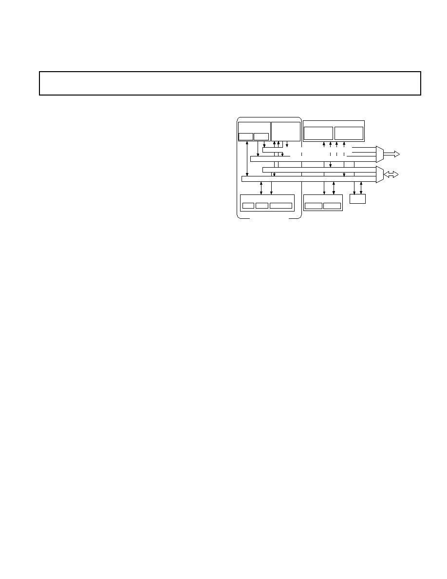
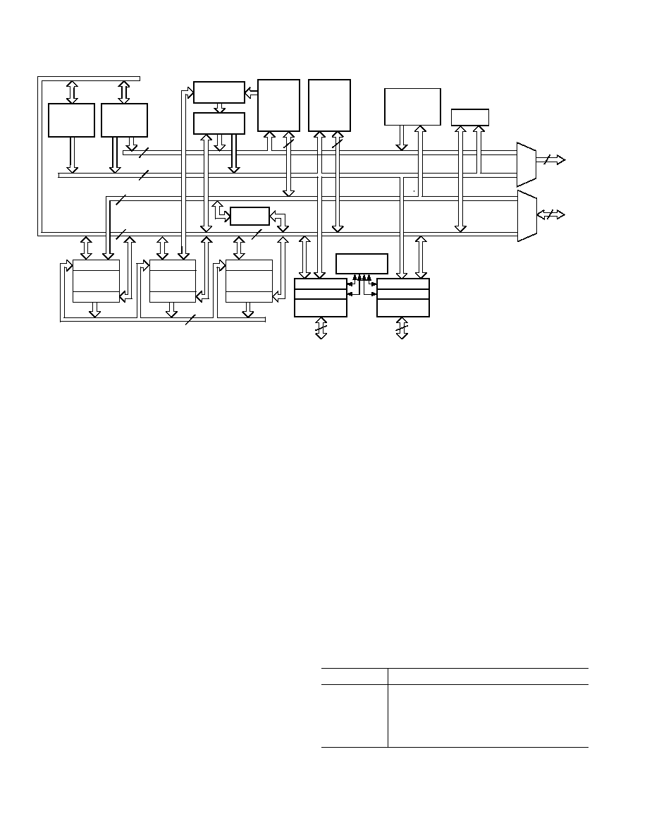
ARCHITECTURE OVERVIEW
Figure 1 shows a block diagram of the ADSP-216x architecture.
The processors contain three independent computational units:
the ALU, the multiplier/accumulator (MAC), and the shifter.
The computational units process 16-bit data directly and have
provisions to support multiprecision computations. The ALU
performs a standard set of arithmetic and logic operations;
division primitives are also supported. The MAC performs
single-cycle multiply, multiply/add, and multiply/subtract opera-
tions. The shifter performs logical and arithmetic shifts, normal-
ization, denormalization, and derive exponent operations. The
shifter can be used to efficiently implement numeric format control
including multiword floating-point representations.
The internal result (R) bus directly connects the computational
units so that the output of any unit may be used as the input of
any unit on the next cycle.
A powerful program sequencer and two dedicated data address
generators ensure efficient use of these computational units.
The sequencer supports conditional jumps, subroutine calls,
and returns in a single cycle. With internal loop counters and
loop stacks, the ADSP-216x executes looped code with zero
overhead--no explicit jump instructions are required to main-
tain the loop.
Two data address generators (DAGs) provide addresses for
simultaneous dual operand fetches (from data memory and
program memory). Each DAG maintains and updates four
address pointers. Whenever the pointer is used to access data
(indirect addressing), it is post-modified by the value of one of
four modify registers. A length value may be associated with
each pointer to implement automatic modulo addressing for
circular buffers. The circular buffering feature is also used by
the serial ports for automatic data transfers to (and from) on-
chip memory.
EZ-ICE and EZ-LAB are registered trademarks of Analog Devices, Inc.
REV. 0
ADSP-216x
4
Efficient data transfer is achieved with the use of five internal
buses:
·
Program Memory Address (PMA) Bus
·
Program Memory Data (PMD) Bus
·
Data Memory Address (DMA) Bus
·
Data Memory Data (DMD) Bus
·
Result (R) Bus
The two address buses (PMA, DMA) share a single external
address bus, allowing memory to be expanded off-chip, and the
two data buses (PMD, DMD) share a single external data bus.
The
BMS, DMS and PMS signals indicate which memory space
is using the external buses.
Program memory can store both instructions and data, permit-
ting the ADSP-216x to fetch two operands in a single cycle,
one from program memory and one from data memory. The
processor can fetch an operand from on-chip program memory
and the next instruction in the same cycle.
The memory interface supports slow memories and memory-
mapped peripherals with programmable wait state generation.
External devices can gain control of the processor's buses with
the use of the bus request/grant signals (
BR, BG).
One bus grant execution mode (GO Mode) allows the ADSP-
216x to continue running from internal memory. A second
execution mode requires the processor to halt while buses are
granted.
Each ADSP-216x processor can respond to several different
interrupts. There can be up to three external interrupts,
configured as edge- or level-sensitive. Internal interrupts can be
generated by the timer and serial ports. There is also a master
RESET signal.
Booting circuitry provides for loading on-chip program memory
automatically from byte-wide external memory. After reset,
three wait states are automatically generated. This allows, for
example, a 60 ns ADSP-2161 to use a 200 ns EPROM as
external boot memory. Multiple programs can be selected and
loaded from the EPROM with no additional hardware.
The data receive and transmit pins on SPORT1 (Serial Port 1)
can be alternatively configured as a general-purpose input flag
and output flag. You can use these pins for event signalling to
and from an external device.
A programmable interval timer can generate periodic interrupts.
A 16-bit count register (TCOUNT) is decremented every n
cycles, where n1 is a scaling value stored in an 8-bit register
(TSCALE). When the value of the count register reaches zero,
an interrupt is generated and the count register is reloaded from
a 16-bit period register (TPERIOD).
Serial Ports
The ADSP-216x processors include two synchronous serial
ports (SPORTs) for serial communications and multiprocessor
communication. All of the ADSP-216x processors have two
serial ports (SPORT0, SPORT1).
The serial ports provide a complete synchronous serial interface
with optional companding in hardware. A wide variety of
framed or frameless data transmit and receive modes of opera-
tion are available. Each SPORT can generate an internal pro-
grammable serial clock or accept an external serial clock.
Each serial port has a 5-pin interface consisting of the following
signals:
Signal Name
Function
SCLK
Serial Clock (I/O)
RFS
Receive Frame Synchronization (I/O)
TFS
Transmit Frame Synchronization (I/O)
DR
Serial Data Receive
DT
Serial Data Transmit
OUTPUT REGS
INPUT REGS
OUTPUT REGS
INPUT REGS
OUTPUT REGS
INPUT REGS
DATA
ADDRESS
GENERATOR
#1
DATA
ADDRESS
GENERATOR
#2
INSTRUCTION
REGISTER
PROGRAM
SEQUENCER
PROGRAM
MEMORY
SRAM
& ROM
BOOT
ADDRESS
GENERATOR
TIMER
PMA BUS
DMA BUS
PMD BUS
DMD BUS
24
16
BUS
EXCHANGE
COMPANDING
CIRCUITRY
TRANSMIT REG
RECEIVE REG
SERIAL
PORT 1
TRANSMIT REG
RECEIVE REG
SERIAL
PORT 0
5
5
16
R BUS
ALU
MAC
SHIFTER
PMA BUS
14
14 PMA BUS
DATA
MEMORY
SRAM
EXTERNAL
DATA
BUS
EXTERNAL
ADDRESS
BUS
MUX
MUX
24
14
24 PMA BUS
16 PMA BUS
16
Figure 1. ADSP-216x Block Diagram

REV. 0
ADSP-216x
5
The ADSP-216x serial ports offer the following capabilities:
Bidirectional--Each SPORT has a separate, double-buffered
transmit and receive function.
Flexible Clocking--Each SPORT can use an external serial
clock or generate its own clock internally.
Flexible Framing--The SPORTs have independent framing
for the transmit and receive functions; each function can run in
a frameless mode or with frame synchronization signals inter-
nally generated or externally generated; frame sync signals may
be active high or inverted, with either of two pulsewidths and
timings.
Different Word Lengths--Each SPORT supports serial data
word lengths from 3 to 16 bits.
Companding in Hardware--Each SPORT provides optional
A-law and
µ
-law companding according to CCITT recommen-
dation G.711.
Flexible Interrupt Scheme--Receive and transmit functions
can generate a unique interrupt upon completion of a data word
transfer.
Autobuffering with Single-Cycle Overhead--Each SPORT
can automatically receive or transmit the contents of an entire
circular data buffer with only one overhead cycle per data word;
an interrupt is generated after the transfer of the entire buffer is
completed.
Multichannel Capability (SPORT0 Only)--SPORT0 pro-
vides a multichannel interface to selectively receive or transmit a
24-word or 32-word, time-division multiplexed serial bit stream;
this feature is especially useful for T1 or CEPT interfaces, or as
a network communication scheme for multiple processors.
Alternate Configuration--SPORT1 can be alternatively
configured as two external interrupt inputs (
IRQ0, IRQ1) and
the Flag In and Flag Out signals (FI, FO).
Interrupts
The ADSP-216x's interrupt controller lets the processor re-
spond to interrupts with a minimum of overhead. Up to three
external interrupt input pins,
IRQ0, IRQ1 and IRQ2, are pro-
vided.
IRQ2 is always available as a dedicated pin; IRQ1 and
IRQ0 may be alternately configured as part of Serial Port 1. The
ADSP-216x also supports internal interrupts from the timer and
the serial ports. The interrupts are internally prioritized and
individually maskable (except for
RESET which is nonmaskable).
The
IRQx input pins can be programmed for either level- or
edge-sensitivity. The interrupt priorities for each ADSP-216x
processor are shown in Table II.
Table II. Interrupt Vector Addresses and Priority
Interrupt
ADSP-216x Interrupt Source
Vector Address
RESET Startup
0x0000
IRQ2 or Power-Down
0x0004 (High Priority)
SPORT0 Transmit
0x0008
SPORT0 Receive
0x000C
SPORT1 Transmit or
IRQ1
0x0010
SPORT1 Receive or
IRQ0
0x0014
Timer
0x0018 (Low Priority)
The ADSP-216x uses a vectored interrupt scheme: when an
interrupt is acknowledged, the processor shifts program control
to the interrupt vector address corresponding to the interrupt
received. Interrupts can be optionally nested so that a higher
priority interrupt can preempt the currently executing interrupt
service routine. Each interrupt vector location is four instruc-
tions in length so that simple service routines can be coded
entirely in this space. Longer service routines require an addi-
tional JUMP or CALL instruction.
Individual interrupt requests are logically ANDed with the bits
in the IMASK register; the highest-priority unmasked interrupt
is then selected.
The interrupt control register,
ICNTL, allows the external
interrupts to be set as either edge- or level-sensitive. Depending
on Bit 4 in
ICNTL, interrupt service routines can either be
nested (with higher priority interrupts taking precedence) or be
processed sequentially (with only one interrupt service active at
a time).
The interrupt force and clear register, IFC, is a write-only regis-
ter that contains a force bit and a clear bit for each interrupt.
When responding to an interrupt, the ASTAT, MSTAT and
IMASK status registers are pushed onto the status stack and
the PC counter is loaded with the appropriate vector address.
The status stack is seven levels deep to allow interrupt nesting.
The stack is automatically popped when a return from the inter-
rupt instruction is executed.
Pin Definitions
Pin Function Descriptions show pin definitions for the ADSP-
216x processors. Any inputs not used must be tied to V
DD
.
SYSTEM INTERFACE
Figure 3 shows a typical system for the ADSP-216x with two
serial I/O devices, an optional external program and data
memory. A total of 12K words of data memory and 15K words
of program memory is addressable.
Programmable wait-state generation allows the processors to
easily interface to slow external memories.
The ADSP-216x processors also provide either: one external
interrupt (
IRQ2) and two serial ports (SPORT0, SPORT1), or
three external interrupts (
IRQ2, IRQ1, IRQ0) and one serial
port (SPORT0).
Clock Signals
The ADSP-216x processors' CLKIN input may be driven by a
crystal or by a TTL-compatible external clock signal. The
CLKIN input may not be halted or changed in frequency during
operation, nor operated below the specified low frequency limit.
If an external clock is used, it should be a TTL-compatible
signal running at the instruction rate. The signal should be
connected to the processor's CLKIN input; in this case, the
XTAL input must be left unconnected.
Because the ADSP-216x processors include an on-chip oscilla-
tor circuit, an external crystal may also be used. The crystal
should be connected across the CLKIN and XTAL pins, with
two capacitors connected as shown in Figure 2. A parallel-
resonant, fundamental frequency, microprocessor-grade crystal
should be used.

REV. 0
ADSP-216x
6
CLKIN
CLKOUT
XTAL
ADSP-216x
Figure 2. External Crystal Connections
A clock output signal (CLKOUT) is generated by the processor,
synchronized to the processor's internal cycles.
Reset
The
RESET signal initiates a complete reset of the ADSP-216x.
The
RESET signal must be asserted when the chip is powered
up to assure proper initialization. If the
RESET signal is applied
during initial power-up, it must be held long enough to allow
the processor's internal clock to stabilize. If
RESET is activated
at any time after power-up and the input clock frequency does
not change, the processor's internal clock continues and does
not require this stabilization time.
The power-up sequence is defined as the total time required for
the crystal oscillator circuit to stabilize after a valid V
DD
is
applied to the processor and for the internal phase-locked loop
(PLL) to lock onto the specific crystal frequency. A minimum of
2000 t
CK
cycles will ensure that the PLL has locked (this does
not, however, include the crystal oscillator start-up time).
During this power-up sequence the
RESET signal should be
held low. On any subsequent resets, the
RESET signal must
meet the minimum pulsewidth specification, t
RSP
.
To generate the
RESET signal, use either an RC circuit with an
external Schmidt trigger or a commercially available reset IC.
(Do not use only an RC circuit.)
The
RESET input resets all internal stack pointers to the empty
stack condition, masks all interrupts, and clears the MSTAT
register. When
RESET is released, the boot loading sequence is
performed (provided there is no pending bus request and the chip
is configured for booting, with MMAP = 0). The first instruction is
then fetched from internal program memory location 0x0000.
PIN FUNCTION DESCRIPTIONS
Pin
# of
Input/
Name(s)
Pins
Output
Function
Address
14
O
Address outputs for program, data and boot memory.
Data
1
24
I/O
Data I/O pins for program and data memories. Input only for
boot memory, with two MSBs used for boot memory addresses.
Unused data lines may be left floating.
RESET
1
I
Processor Reset Input
IRQ2
1
I
External Interrupt Request #2
BR
2
1
I
External Bus Request Input
BG
1
O
External Bus Grant Output
PMS
1
O
External Program Memory Select
DMS
1
O
External Data Memory Select
BMS
1
O
Boot Memory Select
RD
1
O
External Memory Read Enable
WR
1
O
External Memory Write Enable
MMAP
1
I
Memory Map Select Input
CLKIN, XTAL
2
I
External Clock or Quartz Crystal Input
CLKOUT
1
O
Processor Clock Output
V
DD
Power Supply Pins
GND
Ground Pins
SPORT0
5
I/O
Serial Port 0 Pins (TFS0, RFS0, DT0, DR0, SCLK0)
SPORT1
5
I/O
Serial Port 1 Pins (TFS1, RFS1, DT1, DR1, SCLK1)
or Interrupts and Flags:
IRQ0 (RFS1)
1
I
External Interrupt Request #0
IRQ1 (TFS1)
1
I
External Interrupt Request #1
FI (DR1)
1
I
Flag Input Pin
FO (DT1)
1
O
Flag Output Pin
PWDACK
3
1
O
Indicates when the processor has entered power-down.
PWDFLAG
3
1
I
Low-to-High Transition of the Power-Down Flag. Input pin can
be used to terminate power-down.
NOTES
1
Unused data bus lines may be left floating.
2
BR must be tied high (to V
DD
) if not used.
3
Only on ADSP-2165/ADSP-2166.
REV. 0
ADSP-216x
7
Program Memory Interface
The on-chip program memory address bus (PMA) and on-chip
program memory data bus (PMD) are multiplexed with the on-
chip data memory buses (DMA, DMD), creating a single exter-
nal data bus and a single external address bus. The external
data bus is bidirectional and is 24 bits wide to allow instruction
fetches from external program memory. Program memory may
contain code and data.
The external address bus is 14 bits wide. For the ADSP-216x,
these lines can directly address up to 16K words, of which 2K
are on-chip.
The data lines are bidirectional. The program memory select
(
PMS) signal indicates accesses to program memory and can be
used as a chip select signal. The write (
WR) signal indicates a
write operation and is used as a write strobe. The read (
RD)
signal indicates a read operation and is used as a read strobe or
output enable signal.
The ADSP-216x processors write data from their 16-bit regis-
ters to 24-bit program memory using the PX register to provide
the lower eight bits. When the processor reads 16-bit data from
24-bit program memory to a 16-bit data register, the lower eight
bits are placed in the PX register.
The program memory interface can generate 0 to 7 wait states for
external memory devices; default is to 7 wait states after
RESET.
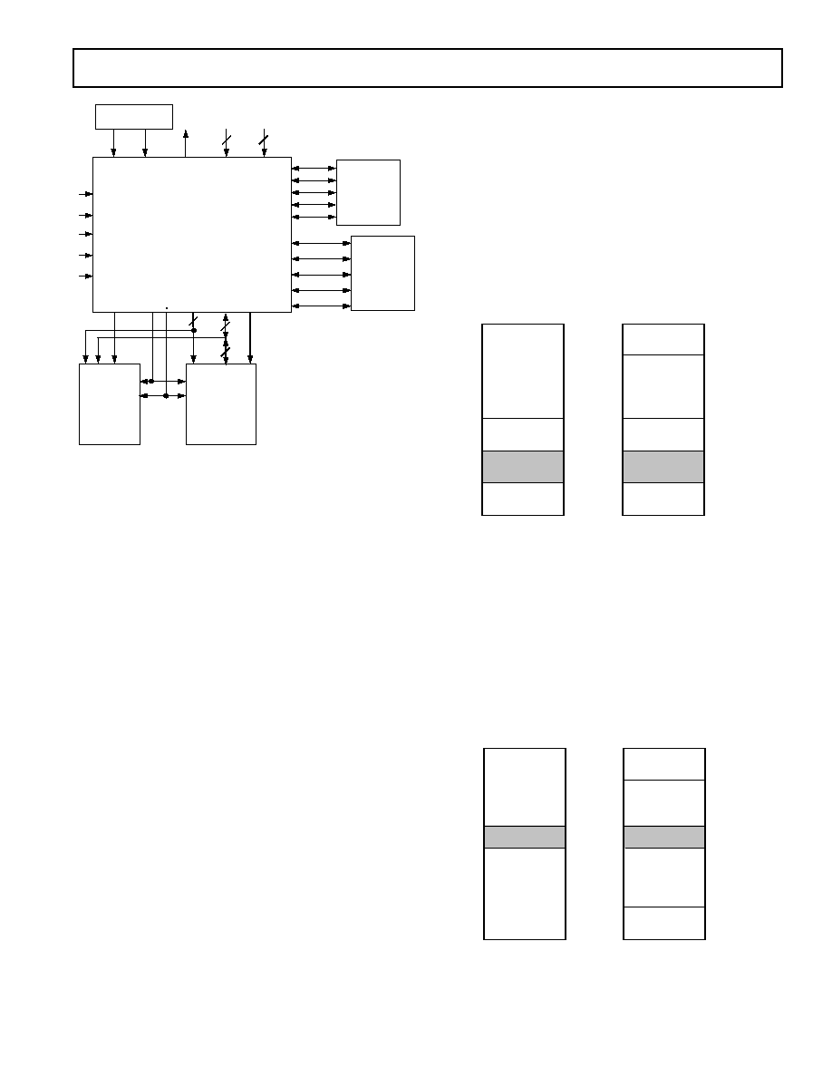
Program Memory Maps
Program memory can be mapped in two ways, depending on the
state of the MMAP pin. Figure 4 shows the program memory
map for the ADSP-2165/ADSP-2166. Figures 5 and 6 show the
program memory maps for the ADSP-2161/ADSP-2162 and
ADSP-2163/ADSP-2164, respectively.
ADSP-2165/ADSP-2166
When MMAP = 0, on-chip program memory ROM occupies
12K words beginning at address 0x0000. Internal program
memory RAM occupies 1K words beginning at address 0x3000.
Off-chip program memory uses the 2K words beginning at
address 0x3800. The ADSP-2165/ADSP-2166 does not support
boot memory.
When MMAP = 1, 2K words of off-chip program memory begin
at address 0x0000. 10K words of on-chip program memory
ROM at 0x800 to 0x2FFF, and the remainder 2K words of
program memory ROM is at 0x3800 to 0x3FFF. Internal pro-
gram memory RAM occupies 1K words at address 0x300 to
0x33FF.
0x0000
2K
EXTERNAL
MMAP = 0
12K 24
INTERNAL
ROM
10K 24
INTERNAL
ROM
1K 24 RAM
RESERVED
2K 24
EXTERNAL
2K 24
INTERNAL
ROM
1K 24 RAM
RESERVED
MMAP = 1
0x2FFF
0x3000
0x33FF
0x3400
0x37FF
0x3800
0x3FFF
0x0000
0x2FFF
0x3000
0x33FF
0x3400
0x37FF
0x3800
0x3FFF
0x07FF
0x0800
Figure 4. ADSP-2165/ADSP-2166 Program Memory Maps
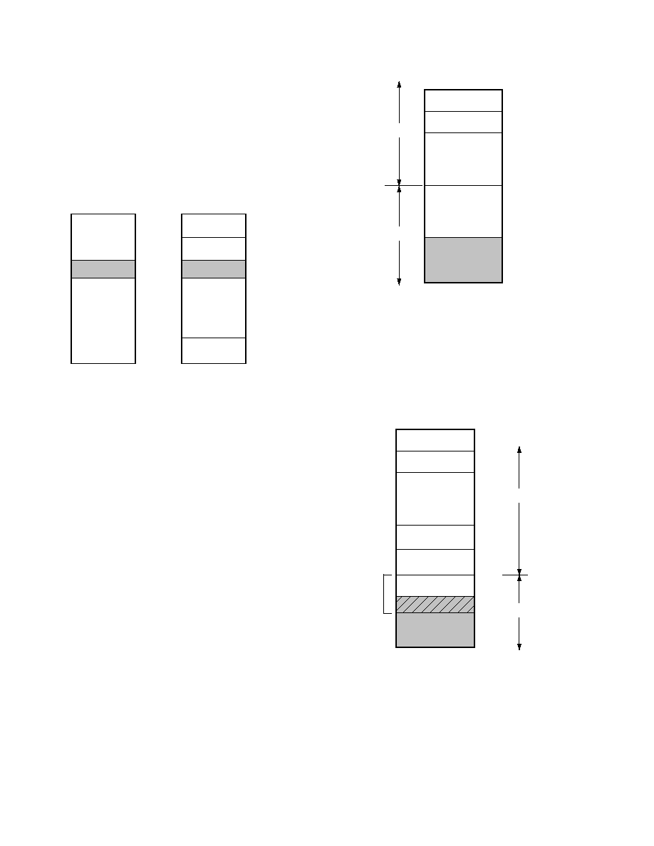
ADSP-2161/ADSP-2162
When MMAP = 0, on-chip program memory ROM occupies
8K words beginning at address 0x0000. Off-chip program
memory uses the remaining 8K words beginning at address
0x2000.
When MMAP = 1, 2K words of off-chip program memory begin
at address 0x0000. 6K words of on-chip program memory ROM
are at 0x0800 to 0x1FF0, and the remainder 2K words of pro-
gram memory ROM is at 0x3800 to 0x3FFF. An additional 6K
of off-chip program memory is at 0x2000 to 0x37FF.
MMAP = 0
8K
INTERNAL
ROM
RESERVED
MMAP = 1
0x0000
0x1FF0
0x1FFF
0x2000
0x3FFF
2K
EXTERNAL
RESERVED
0x0000
0x1FF0
0x1FFF
0x2000
0x3FFF
6K
INTERNAL
ROM
6K
EXTERNAL
2K
INTERNAL
ROM
0x7FFF
0x0800
0x37FF
0x3800
8K
EXTERNAL
Figure 5. ADSP-2161/ADSP-2162 Program Memory Maps
ADSP-216x
RESET
IRQ2
BR
BG
MMAP
SERIAL
PORT 0
SERIAL
PORT 1
PMS
RD
DMS BMS
ADDRESS DATA
CLKIN
XTAL
CLKOUT
V
DD
GND
CLOCK OR
CRYSTAL
3
4
SCLK
SCLK
RFS OR
IRQ0
TFS OR
IRQ1
DT OR FO
DR OR FI
RFS
TFS
DT
DR
SERIAL
DEVICE
(OPTIONAL)
SERIAL
DEVICE
(OPTIONAL)
PROGRAM
MEMORY
(OPTIONAL)
A D
CS
OE
WE
DATA
MEMORY
&
PERIPHERALS
A
D
CS
OE
WE
14
RW
16
D23-8
24
Figure 3. Basic System Configuration
REV. 0
ADSP-216x
8
ADSP-2163/ADSP-2164
When MMAP = 0, on-chip program memory ROM occupies
4K words beginning at address 0x0000. Off-chip program
memory uses the remaining 12K words beginning at address
0x1000.
When MMAP = 1, 2K words of off-chip program memory begin
at address 0x0000. 2K words of on-chip program memory ROM
is at 0x0800 to 0x0FF0, and the remainder 2K words of pro-
gram memory ROM is at 0x3800 to 0x3FFF. An additional
10K of off-chip program memory is at 0x1000 to 0x37FF.
MMAP = 0
4K
INTERNAL
ROM
RESERVED
MMAP = 1
0x0000
0x0FF0
0x0FFF
0x1000
0x3FFF
2K
EXTERNAL
RESERVED
0x0000
0x0FF0
0x0FFF
0x1000
0x3FFF
2K
INTERNAL
ROM
10K
EXTERNAL
2K
INTERNAL
ROM
0x07FF
0x0800
0x37FF
0x3800
12K
EXTERNAL
Figure 6. ADSP-2163/ADSP-2164 Program Memory Maps
Data Memory Interface
The data memory address bus (DMA) is 14 bits wide. The
bidirectional external data bus is 24 bits wide, with the upper 16
bits used for data memory data (DMD) transfers.
The data memory select (DMS) signal indicates access to data
memory and can be used as a chip select signal. The write (WR)
signal indicates a write operation and can be used as a write
strobe. The read (RD) signal indicates a read operation and can
be used as a read strobe or output enable signal.
The ADSP-216x processors support memory-mapped I/O, with
the peripherals memory-mapped into the data memory address
space and accessed by the processor in the same manner as data
memory.
Data Memory Map
For the ADSP-2165/ADSP-2166, on-chip data memory RAM
resides in the 4K words beginning at address 0x2000, as shown
in Figure 7. Data memory locations from 0x3000 to the end of
data memory at 0x3FFF are reserved. Control and status regis-
ters for the system, timer, wait-state configuration, and serial port
operations are located in this region of memory.
The remaining 8K of data memory is located off-chip. This
external data memory is divided into three zones, each associ-
ated with its own wait-state generator. This allows slower pe-
ripherals to be memory-mapped into data memory for which
wait states are specified. By mapping peripherals into different
zones, you can accommodate peripherals with different wait-
state requirements. All zones default to 7 wait states after
RESET.
0x0000
4K 16
MEMORY-MAPPED
REGISTERS
& RESERVED
0x0800
ADDRESS (HEX)
4K 16 INTERNAL
6K EXTERNAL
DWAIT2
1K EXTERNAL
DWAIT0
1K EXTERNAL
DWAIT1
0x0400
0x2000
0x3000
0x3FFF
EXTERNAL
RAM
INTERNAL
RAM
Figure 7. ADSP-2165/ADSP-2166 Data Memory Map
ADSP-2161/ADSP-2162/ADSP-2163/ADSP-2164
For the ADSP-2161/ADSP-2162/ADSP-2163/ADSP-2164, on-
chip data memory RAM resides in the 512 words beginning at
address 0x3800, also shown in Figure 8. Data memory locations
from 0x3A00 to the end of data memory at 0x3FFF are reserved.
Control and status registers for the system, timer, wait-state
configuration, and serial port operations are located in this
region of memory.
0x0000
512
ADSP-2161/62/63/64
0x0800
ADDRESS (HEX)
10K EXTERNAL
DWAIT2
1K EXTERNAL
DWAIT0
1K EXTERNAL
DWAIT1
0x0400
0x3000
0x3C00
0x3FFF
EXTERNAL
RAM
INTERNAL
RAM
1K EXTERNAL
DWAIT3
1K EXTERNAL
DWAIT4
MEMORY-MAPPED
CONTROL REGISTERS
& RESERVED
0x3A00
0x3800
0x3400
Figure 8. ADSP-2161/ADSP-2162/ADSP-2163/ADSP-2164
Data Memory Map
The remaining 14K of data memory is located off-chip. This
external data memory is divided into five zones, each associated
with its own wait-state generator. This allows slower peripherals
to be memory-mapped into data memory for which wait states
are specified. By mapping peripherals into different zones, you
can accommodate peripherals with different wait-state require-
ments. All zones default to seven wait states after
RESET.

REV. 0
ADSP-216x
9
Bus Interface
The ADSP-216x processors can relinquish control of their data
and address buses to an external device. When the external
device requires control of the buses, it asserts the bus request
signal (
BR). If the ADSP-216x is not performing an external
memory access, it responds to the active
BR input in the next
cycle by:
·
Three-stating the data and address buses and the PMS,
DMS, BMS, RD, WR output drivers,
·
Asserting the bus grant (BG) signal, and halting program
execution.
If the Go mode is set, however, the ADSP-216x will not halt
program execution until it encounters an instruction that
requires an external memory access.
If the ADSP-216x is performing an external memory access
when the external device asserts the
BR signal, it will not three-
state the memory interfaces or assert the
BG signal until the
cycle after the access completes (up to eight cycles later depend-
ing on the number of wait states). The instruction does not need
to be completed when the bus is granted; the ADSP-21xx will
grant the bus between two memory accesses if an instruction
requires more than one external memory access.
When the
BR signal is released, the processor releases the BG
signal, re-enables the output drivers and continues program
execution from the point at which it stopped.
The bus request feature operates at all times, including when the
processor is booting and when
RESET is active. If this feature is
not used, the
BR input should be tied high (to V
DD
).
POWER-DOWN
The ADSP-2165/ADSP-2166 processors have a low power
feature that lets the processor enter a very low power dormant
state through hardware or software control. A list of power-
down features follows:
·
Processor registers and on-chip memory contents are main-
tained during power-down.
·
Power-down mode holds the processor in CMOS standby
with a maximum current of less than 100
µ
A in some modes.
·
Support for an externally generated TTL or CMOS proces-
sor clock. The external clock can continue running during
power-down without affecting the lowest power rating.
·
Support for crystal operation includes disabling the oscillator
to save power. (The processor automatically waits 4096
CLKIN cycles for the crystal oscillator to start and stabilize).
·
When power-down mode is enabled, powering down of the
processor can be initiated either by externally generated
IRQ2 interrupt or by using the IRQ2 force bit in the IFC
register.
·
Power-Down Acknowledge Pin (PWDACK) indicates when
the processor has entered power-down.
·
Interrupt support allows an unlimited number of instructions
to be executed before optionally powering down.
·
Context clear/save control allows the processor to continue
where it left off or start with a clean context when leaving the
power-down state.
·
Low-to-high transition of the power-down flag input pin
(PWDFLAG) can be used to terminate power-down.
·
The
RESET pin also can also be used to terminate
power-down.
Power-Down Control
Several parameters of power-down operation can be controlled
through control bits of the "power-down/sportl autobuffer con-
trol register." This control register is memory-mapped at loca-
tion 0x3FEF and the power-down control bits are as follows:
bit[15] xtal: xtal pin disable during power-down
1 = disabled, 0 = enable (default)
bit[14] pwdflag: (read only )
when pwdena = 1, the value of bit [14] pwdflag is equal to the
status of the pwdflag input pin.
when pwdena = 0, the value of bit [14] pwdflag is equal to 0.
bit[13] pwdena: power-down enable
1 = enable, 0 = disable (default)
if pwdena is set to 0, then the output pin PWDACK is driven
low and the input pin PWDFLAG is disabled
Note: It is not recommended that power-down enable be set or
cleared during an
IRQ2 interrupt.
bit[12] pucr: power-up context reset
1 = soft reset, 0 = resume execution (default)
Entering Power-Down
The power-down sequence is defined as follows:
·
Enable power-down logic by setting the pwdena bit in the
power-down/sportl autobuffer control register.
Note: In order to power-down, the PWDENA bit must be set
before the
IRQ2 interrupt is initiated.
·
Initiate the power-down sequence by generating an
IRQ2
interrupt either externally or by software use of the IFC
register.
·
The processor vectors to the
IRQ2 interrupt vector located at
0x0004.
·
Any number of housekeeping instructions, starting at loca-
tion 0x0004 can be executed prior to the processor entering
the power-down mode.
·
The processor enters the power-down mode when the pro-
cessor executes an IDLE instruction while executing the
IRQ2 interrupt routine.
Notes:
·
If an RTI instruction is executed before the processor en-
counter an IDLE instruction, then the processor returns
from the
IRQ2 interrupt and the power-down sequence is
aborted.
·
The user can differentiate between a "normal"
IRQ2 inter-
rupt and a "power-down"
IRQ2 interrupt by resetting the
PWDFLAG pin and checking the status of this pin by testing
the PWDFLAG bit in the power-down/SPORT1 autobuffer
control register located at DM[0x3FEF].

REV. 0
ADSP-216x
10
Exiting Power-Down
The power-down mode can be exited with the use of the
PWDFLAG or RESET pin. Applying a low-to-high transition to
the PWDFLAG pin takes the processor out of power-down
mode. In this case, a delay of 4096 cycles is automatically in-
duced by the processor. Also, depending on the status of the
power-up context reset bit (pucr), the processor either
1) continues to execute instructions following the IDLE instruc-
tion that caused the power-down. A RTI instruction is re-
quired to pass control back to the main routine (pucr = 0)
or
2) resumes operation from power-down by clearing the PC,
STATUS, LOOP and CNTR stack. The IMASK and
ASTAT registers are set to 0 and the SSTAT goes to 0x55.
The processor then starts executing instructions from the
address zero (pucr = 1).
In the case where the power-down mode is exited by asserting
the
RESET pin, the processor state is reset and instruction are
executed from address 0x0000. The
RESET pin in this case
must be held low long enough for the external crystal (if any)
and the on-chip PLL to stabilize and lock.
Low Power IDLE Instruction
The IDLE instruction places the ADSP-216x processor in low
power state in which it waits for an interrupt. When an interrupt
occurs, it is serviced and execution continues with instruction
following IDLE. Typically this next instruction will be a JUMP
back to the IDLE instruction. This implements a low power
standby loop.
The IDLE n instruction is a special version of IDLE that slows
the processor's internal clock signal to further reduce power
consumption. The reduced clock frequency, a programmable
fraction of the normal clock rate, is specified by a selectable
divisor, n, given in the IDLE instruction. The syntax of the
instruction is:
IDLE n;
where n = 16, 32, 64 or 128.
The instruction leaves the chip in an idle state, operating at the
slower rate. While it is in this state, the processor's other inter-
nal clock signals, such as SCLK, CLKOUT, and the timer
clock, are reduced by the same ratio. Upon receipt of an en-
abled interrupt, the processor will stay in the IDLE state for up
to a maximum of n CLKIN cycles, where n is the divisor speci-
fied in the instruction, before resuming normal operation.
When the IDLE n instruction is used, it slows the processor's
internal clock and thus its response time to incoming interrupts
the 1-cycle response time of the standard IDLE state is increased
by n, the clock divisor. When an enabled interrupt is received,
the ADSP-216x will remain in the IDLE state for up to a maxi-
mum of n CLKIN cycles (where n = 16, 32, 64 or 128) before
resuming normal operation.
When the IDLE n instruction is used in systems that have an
externally generated serial clock (SCLK), the serial clock rate
may be faster than the processor's reduced internal clock rate.
Under these conditions, interrupts must not be generated at a
faster rate than can be serviced, due to the additional time the
processor takes to come out of the IDLE state (a maximum of n
CLKIN cycles).
ADSP-216x Prototyping
You can prototype your ADSP-216x system with either ADSP-
2101 or ADSP-2103 RAM-based processors. When code is fully
developed and debugged, it can be submitted to Analog Devices
for conversion into an ADSP-216x ROM product.
The ADSP-2101 EZ-ICE emulator can be used for development
of ADSP-216x systems. For the 3.3 V ADSP-2162/ADSP-2164
and ADSP-2166, a voltage converter interface board provides
3.3 V emulation.
Additional overlay memory is used for emulation of ADSP-
2161/ADSP-2162 systems. It should be noted that due to the
use of off-chip overlay memory to emulate the ADSP-2161/
ADSP-2162, a performance loss may be experienced when both
executing instructions and fetching program memory data from
the off-chip overlay memory in the same cycle. This can be
overcome by locating program memory data in on-chip memory.
Ordering Procedure for ADSP-216x ROM Processors
To place an order for a custom ROM-coded ADSP-2161,
ADSP-2162, ADSP-2163, ADSP-2164 , ADSP-2165 or ADSP-
2166 processor, you must:
1. Complete the following forms contained in the ADSP ROM
Ordering Package, available from your Analog Devices sales
representative:
ADSP-216x ROM Specification Form
ROM Release Agreement
ROM NRE Agreement & Minimum Quantity Order (MQO)
Acceptance Agreement for Preproduction ROM Products
2. Return the forms to Analog Devices along with two copies of the
Memory Image File (.EXE file) of your ROM code. The files must
be supplied on two 3.5" or 5.25" floppy disks for the IBM PC
(DOS 2.01 or higher).
3. Place a purchase order with Analog Devices for nonrecurring
engineering changes (NRE) associated with ROM product
development.
After this information is received, it is entered into Analog
Devices' ROM Manager System which assigns a custom ROM
model number to the product. This model number will be
branded on all prototype and production units manufactured to
these specifications.
To minimize the risk of code being altered during this process,
Analog Devices verifies that the .EXE files on both floppy disks
are identical, and recalculates the checksums for the .EXE file
entered into the ROM Manager System. The checksum data, in
the form of a ROM Memory Map, a hard copy of the .EXE file,
and a ROM Data Verification form are returned to you for
inspection.
A signed ROM Verification Form and a purchase order for
production units are required prior to any product being manu-
factured. Prototype units may be applied toward the minimum
order quantity.
Upon completion of prototype manufacture, Analog Devices
will ship prototype units and a delivery schedule update for
production units. An invoice against your purchase order for the
NRE charges is issued at this time.
There is a charge for each ROM mask generated and a mini-
mum order quantity. Consult your sales representative for de-
tails. A separate order must be placed for parts of a specific
package type, temperature range, and speed grade.

REV. 0
ADSP-216x
11
Instruction Set
The ADSP-216x assembly language uses an algebraic syntax for
ease of coding and readability. The sources and destinations of
computations and data movements are written explicitly in each
assembly statement, eliminating cryptic assembler mnemonics.
Every instruction assembles into a single 24-bit word and executes
in a single cycle. The instructions encompass a wide variety of
instruction types along with a high degree of operational
parallelism. There are five basic categories of instructions: data
move instructions, computational instructions, multifunction
instructions, program flow control instructions and miscella-
neous instructions. Multifunction instructions perform one or
two data moves and a computation.
The instruction set is summarized below. The ADSP-2100
Family Users Manual contains a complete reference to the
instruction set.
ALU Instructions
[IF cond]
AR|AF
=
xop + yop [+ C] ;
Add/Add with Carry
=
xop yop [+ C 1] ;
Subtract X Y/Subtract X Y with Borrow
=
yop xop [+ C 1] ;
Subtract Y X/Subtract Y X with Borrow
=
xop AND yop ;
AND
=
xop OR yop ;
OR
=
xop XOR yop ;
XOR
=
PASS xop ;
Pass, Clear
=
xop ;
Negate
=
NOT xop ;
NOT
=
ABS xop ;
Absolute Value
=
yop + 1 ;
Increment
=
yop 1 ;
Decrement
=
DIVS yop, xop ;
Divide
=
DIVQ xop ;
MAC Instructions
[IF cond]
MR|MF =
xop
*
yop ;
Multiply
=
MR + xop
*
yop ;
Multiply/Accumulate
=
MR xop
*
yop ;
Multiply/Subtract
=
MR ;
Transfer MR
=
0 ;
Clear
IF MV SAT MR ;
Conditional MR Saturation
Shifter Instructions
[IF cond]
SR = [SR OR] ASHIFT xop ;
Arithmetic Shift
[IF cond]
SR = [SR OR] LSHIFT xop ;
Logical Shift
SR = [SR OR] ASHIFT xop BY <exp>;
Arithmetic Shift Immediate
SR = [SR OR] LSHIFT xop BY <exp>;
Logical Shift Immediate
[IF cond]
SE = EXP xop ;
Derive Exponent
[IF cond]
SB = EXPADJ xop ;
Block Exponent Adjust
[IF cond]
SR = [SR OR] NORM xop ;
Normalize
Data Move Instructions
reg = reg ;
Register-to-Register Move
reg = <data> ;
Load Register Immediate
reg = DM (<addr>) ;
Data Memory Read (Direct Address)
dreg = DM (Ix , My) ;
Data Memory Read (Indirect Address)
dreg = PM (Ix , My) ;
Program Memory Read (Indirect Address)
DM (<addr>) = reg ;
Data Memory Write (Direct Address)
DM (Ix , My) = dreg ;
Data Memory Write (Indirect Address)
PM (Ix , My) = dreg ;
Program Memory Write (Indirect Address)
Multifunction Instructions
<ALU>|<MAC>|<SHIFT> , dreg = dreg ;
Computation with Register-to-Register Move
<ALU>|<MAC>|<SHIFT> , dreg = DM (Ix , My) ;
Computation with Memory Read
<ALU>|<MAC>|<SHIFT> , dreg = PM (Ix , My) ;
Computation with Memory Read
DM (Ix , My) = dreg , <ALU>|<MAC>|<SHIFT> ;
Computation with Memory Write
PM (Ix , My) = dreg , <ALU>|<MAC>|<SHIFT> ;
Computation with Memory Write
dreg = DM (Ix , My) , dreg = PM (Ix , My) ;
Data & Program Memory Read
<ALU>|<MAC> , dreg = DM (Ix , My) , dreg = PM (Ix , My) ;
ALU/MAC with Data & Program Memory Read

REV. 0
ADSP-216x
12
Program Flow Instructions
DO <addr> [UNTIL term] ;
Do Until Loop
[IF cond] JUMP (Ix) ;
Jump
[IF cond] JUMP <addr>;
[IF cond] CALL (Ix) ;
Call Subroutine
[IF cond] CALL <addr>;
IF [NOT ] FLAG_IN
JUMP <addr>;
Jump/Call on Flag In Pin
IF [NOT ] FLAG_IN
CALL <addr>;
[IF cond] SET|RESET|TOGGLE
FLAG_OUT [, ...] ;
Modify Flag Out Pin
[IF cond] RTS ;
Return from Subroutine
[IF cond] RTI ;
Return from Interrupt Service Routine
IDLE [(n)] ;
Idle
Miscellaneous Instructions
NOP ;
No Operation
MODIFY (Ix , My);
Modify Address Register
[PUSH STS] [, POP CNTR] [, POP PC] [, POP LOOP] ;
Stack Control
ENA|DIS
SEC_REG [, ...] ;
Mode Control
BIT_REV
AV_LATCH
AR_SAT
M_MODE
TIMER
G_MODE
Notation Conventions
Ix
Index registers for indirect addressing
My
Modify registers for indirect addressing
<data>
Immediate data value
<addr>
Immediate address value
<exp>
Exponent (shift value) in shift immediate instructions (8-bit signed number)
<ALU>
Any ALU instruction (except divide)
<MAC>
Any multiply-accumulate instruction
<SHIFT>
Any shift instruction (except shift immediate)
cond
Condition code for conditional instruction
term
Termination code for DO UNTIL loop
dreg
Data register (of ALU, MAC, or Shifter)
reg
Any register (including dregs)
;
A semicolon terminates the instruction
,
Commas separate multiple operations of a single instruction
[ ]
Optional part of instruction
[, ...]
Optional, multiple operations of an instruction
option1 | option2
List of options; choose one.
Assembly Code Example
The following example is a code fragment that performs the filter tap update for an adaptive filter based on a least-mean-squared
algorithm. Notice that the computations in the instructions are written like algebraic equations.
MF=MX0*MY1(RND), MX0=DM(I2,M1);
{MF=error*beta}
MR=MX0*MF(RND), AY0=PM(I6,M5);
DO adapt UNTIL CE;
AR=MR1+AY0, MX0=DM(I2,M1), AY0=PM(I6,M7);
adapt:
PM(I6,M6)=AR, MR=MX0*MF(RND);
MODIFY(I2,M3);
{Point to oldest data}
MODIFY(I6,M7);
{Point to start of data}

REV. 0
13
ADSP-216x
SPECIFICATIONS
ADSP-2161/ADSP-2163/ADSP-2165RECOMMENDED OPERATING CONDITIONS
K
Grade
B
Grade
Parameter
Min
Max
Min
Max
Unit
V
DD
Supply Voltage
4.50
5.50
4.50
5.50
V
T
AMB
Ambient Operating Temperature
0
+70
40
+85
°
C
See "Environmental Conditions" for information on thermal specifications.
ELECTRICAL CHARACTERISTICS
Parameter
Test Conditions
Min
Max
Unit
V
IH
Hi-Level Input Voltage
1, 2
@ V
DD
= max
2.0
V
V
IH
Hi-Level CLKIN and Reset Voltage
@ V
DD
= max
2.2
V
V
IL
Lo-Level Input Voltage
1, 3
@ V
DD
= min
0.8
V
V
OH
Hi-Level Output Voltage
1, 4, 5
@ V
DD
= min, I
OH
= 0.5 mA
2.4
V
@ V
DD
= min, I
OH
= 100
µ
A
6
V
DD
0.3
V
V
OL
Lo-Level Output Voltage
1, 4, 5
@ V
DD
= min, I
OL
= 2 mA
0.4
V
I
IH
Hi-Level Input Current
3
@ V
DD
= max, V
IN
= V
DD
max
10
µ
A
I
IL
Lo-Level Input Current
3
@ V
DD
= max, V
IN
= 0 V
10
µ
A
I
OZH
Three-State Leakage Current
7
@ V
DD
= max, V
IN
= V
DD
max
8
10
µ
A
I
OZL
Three-State Leakage Current
7
@ V
DD
= max, V
IN
= 0 V
8
10
µ
A
C
I
Input Pin Capacitance
3, 6, 9
@ V
IN
= 2.5 V, f
IN
= 1.0 MHz, T
AMB
= 25
°
C
8
pF
C
O
Output Pin Capacitance
6, 7, 9, 10
@ V
IN
= 2.5 V, f
IN
= 1.0 MHz, T
AMB
= 25
°
C
8
pF
NOTES
1
Bidirectional pins: D0D23, SCLK1, RFS1, TFS1, SCLK0, RFS0, TFS0.
2
Input-only pins:
RESET, IRQ2, BR, MMAP, DR1, DR0.
3
Input-only pins: CLKIN,
RESET, IRQ2, BR, MMAP, DR1, DR0.
4
Output pins:
BG, PMS, DMS, BMS, RD, WR, A0A13, CLKOUT, DT1, DT0.
5
Although specified for TTL outputs, all ADSP-21xx outputs are CMOS-compatible and will drive to V
DD
and GND, assuming no dc loads.
6
Guaranteed but not tested.
7
Three-stateable pins: A0A13, D0D23,
PMS, DMS, BMS, RD, WR, DT1, SCLK1, RFS1, TFS1, DT0, SCLK0, RFS0, TFS0.
8
0 V on
BR, CLKIN Active (to force three-state condition).
9
Applies to PLCC, MQFP package types.
10
Output pin capacitance is the capacitive load for any three-stated output pin.
Specifications subject to change without notice.
ABSOLUTE MAXIMUM RATINGS*
Supply Voltage . . . . . . . . . . . . . . . . . . . . . . . . . 0.3 V to +7 V
Input Voltage . . . . . . . . . . . . . . . . . . . . 0.3 V to V
DD
+ 0.3 V
Output Voltage Swing . . . . . . . . . . . . . 0.3 V to V
DD
+ 0.3 V
Operating Temperature Range (Ambient) . . . 40
°
C to +85
°
C
(No Extended Temperature Range)
Storage Temperature Range . . . . . . . . . . . . 65ºC to +150ºC
Lead Temperature (10 sec) PGA . . . . . . . . . . . . . . . . . +300ºC
Lead Temperature (5 sec) PLCC, MQFP, TQFP . . . . +280ºC
*Stresses greater than those listed above may cause permanent damage to the
device. These are stress ratings only; functional operation of the device at these or
any other conditions greater than those indicated in the operational sections of this
specification is not implied. Exposure to absolute maximum rating conditions for
extended periods may affect device reliability.
WARNING!
ESD SENSITIVE DEVICE
CAUTION
ESD (electrostatic discharge) sensitive device. Electrostatic charges as high as 4000 V readily
accumulate on the human body and test equipment and can discharge without detection. Although
the ADSP-216x features proprietary ESD protection circuitry, permanent damage may occur on
devices subjected to high energy electrostatic discharges. Therefore, proper ESD precautions are
recommended to avoid performance degradation or loss of functionality.
REV. 0
ADSP-216x
14
SPECIFICATIONS
ADSP-2161/ADSP-2163/ADSP-2165SUPPLY CURRENT AND POWER
Parameter
Test Conditions
Min
Max
Unit
I
DD
Supply Current (Dynamic)
1
@ V
DD
= max, t
CK
= 40 ns
2
38
mA
@ V
DD
= max, t
CK
= 50 ns
2
31
mA
@ V
DD
= max, t
CK
= 60 ns
2
27
mA
I
DD
Supply Current (Idle)
1, 3
@ V
DD
= max, t
CK
= 40 ns
12
mA
@ V
DD
= max, t
CK
= 50 ns
11
mA
@ V
DD
= max, t
CK
= 60 ns
10
mA
NOTES
1
Current reflects device operating with no output loads.
2
V
IN
= 0.4 V and 2.4 V.
3
Idle refers to ADSP-21xx state of operation during execution of IDLE instruction. Deasserted pins are driven to either V
DD
or GND.
For typical supply current (internal power dissipation) figures, see Figure 9.
Specifications subject to change without notice.
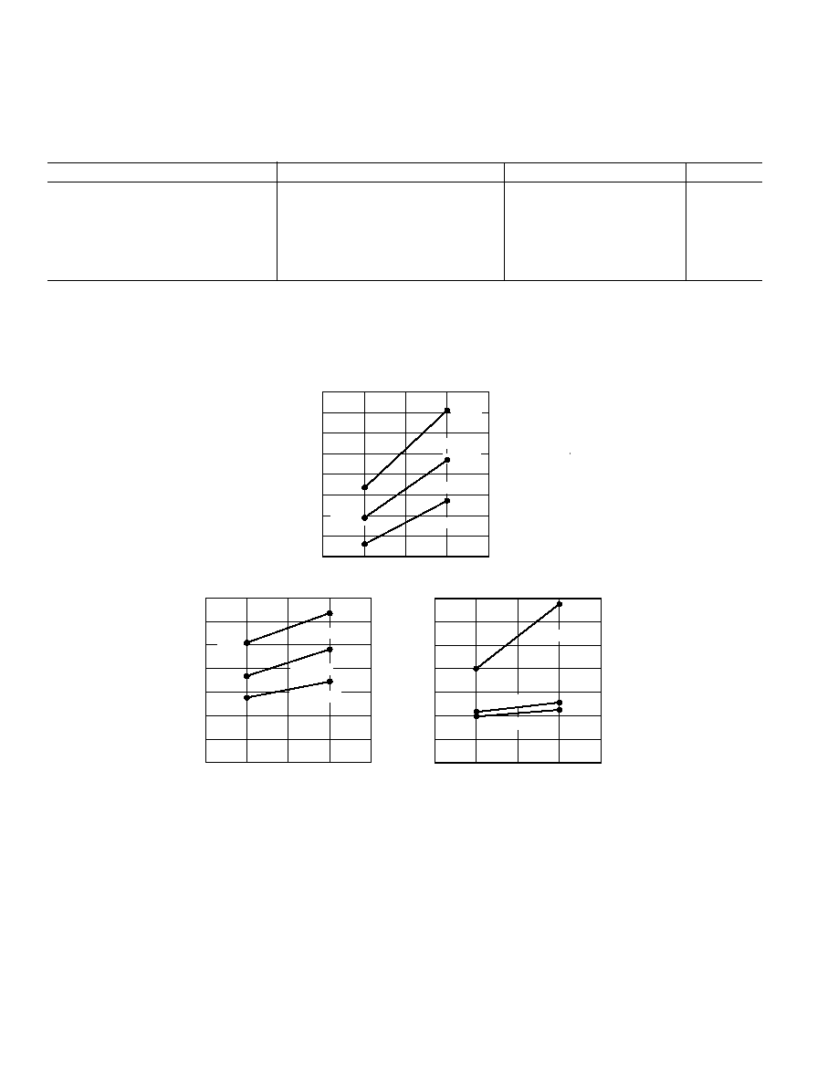
FREQUENCY MHz
220
180
10.00
200
80
60
IDD DYNAMIC
1
V
DD
= 5.5V
V
DD
= 5.0V
V
DD
= 4.5V
205mW
157mW
118mW
129mW
100mW
74mW
POWER mW
160
140
120
100
13.83
20.00
25.00
30.00
FREQUENCY MHz
10
30
20
40
0
IDD IDLE
1,2
V
DD
= 5.5V
V
DD
= 5.0
V
DD
= 4.5V
35mW
51mW
38mW
28mW
POWER mW
49mW
64mW
50
60
70
10.00
13.83
20.00
25.00
30.00
VALID FOR ALL TEMPERATURE GRADES.
1
POWER REFLECTS DEVICE OPERATING WITH NO OUTPUT LOADS.
2
IDLE REFERS TO ADSP-216x OPERATION DURING EXECUTION OF IDLE INSTRUCTION.
DEASSERTED PINS ARE DRIVEN TO EITHER V
DD
OR GND.
3
MAXIMUM POWER DISSIPATION AT V
DD
= 5.5V DURING EXECUTION OF
IDLE n INSTRUCTION.
FREQUENCY MHz
65
40
35
30
IDD IDLE
n MODES
3
64mW
43mW
42mW
51mW
41mW
40mW
POWER mW
45
50
55
60
10.00
13.83
20.00
25.00
30.00
IDLE 16
IDLE 128
IDD IDLE
Figure 9. ADSP-2161/ADSP-2163/ADSP-2165 (Typical) vs. Frequency

REV. 0
ADSP-216x
15
POWER DISSIPATION EXAMPLE
To determine total power dissipation in a specific application,
the following equation should be applied for each output:
C
×
V
DD
2
×
f
C = load capacitance, f = output switching frequency.
Example:
In an ADSP-2161 application where external data memory is
used and no other outputs are active, power dissipation is calcu-
lated as follows:
Assumptions:
·
External data memory is accessed every cycle with 50% of
the address pins switching.
·
External data memory writes occur every other cycle with
50% of the data pins switching.
·
Each address and data pin has a 10 pF total load at the pin.
·
The application operates at V
DD
= 5.0 V and t
CK
= 50 ns.
Total Power Dissipation = P
INT
+ (C
×
V
DD
2
×
f )
P
INT
= internal power dissipation (from Figure 9).
(C
×
V
DD
2
×
f ) is calculated for each output:
# of
Output
Pins
C
V
DD
2
f
Address,
DMS 8
×
10 pF
×
5
2
V
×
20 MHz = 40.0 mW
Data,
WR
9
×
10 pF
×
5
2
V
×
10 MHz = 22.5 mW
RD
1
×
10 pF
×
5
2
V
×
10 MHz = 2.5 mW
CLKOUT
1
×
10 pF
×
5
2
V
×
20 MHz = 5.0 mW
70.0 mW
Total power dissipation for this example = P
INT
+ 70.0 mW.
ENVIRONMENTAL CONDITIONS
Ambient Temperature Rating:
T
AMB
= T
CASE
(PD
×
CA
)
T
CASE
= Case Temperature in
°
C
PD = Power Dissipation in W
CA
= Thermal Resistance (Case-to-Ambient)
JA
= Thermal Resistance (Junction-to-Ambient)
JC
= Thermal Resistance (Junction-to-Case)
Package
JA
JC
CA
PLCC
27
°
C/W
16
°
C/W
11
°
C/W
MQFP
60
°
C/W
18
°
C/W
42
°
C/W
CAPACITIVE LOADING
Figures 10 and 11 show capacitive loading characteristics for the
ADSP-2161/ADSP-2163/ADSP-2165.
C
L
pF
RISE TIME (0.4V 2.0V) ns
0
0
175
25
50
150
1
V
DD
= 4.5V
8
6
4
100
125
75
7
5
3
2
Figure 10. Typical Output Rise Time vs. Load Capacitance, C
L
(at Maximum Ambient Operating Temperature)
C
L
pF
3
0
175
25
50
150
V
DD
= 4.5V
5
3
1
100
125
75
4
2
2
1
0
VALID OUTPUT DELAY OR HOLD ns
Figure 11. Typical Output Valid Delay or Hold vs. Load
Capacitance, C
L
(at Maximum Ambient Operating
Temperature)
ADSP-2161/ADSP-2163/ADSP-2165
REV. 0
ADSP-216x
16
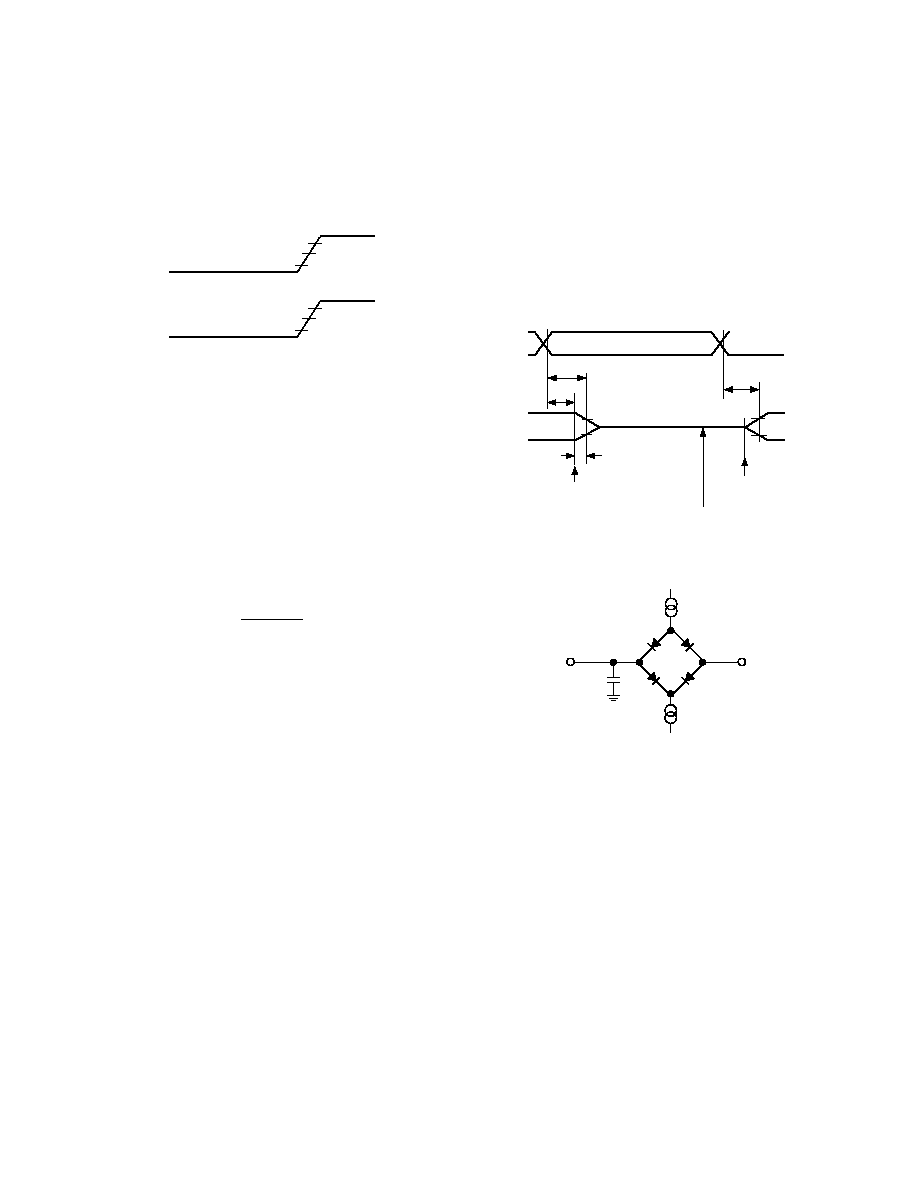
TEST CONDITIONS
Figure 12 shows voltage reference levels for ac measurements.
1.5V
OUTPUT
3.0V
0.0V
INPUT
1.5V
2.0V
0.8V
Figure 12. Voltage Reference Levels for AC Measurements
(Except Output Enable/Disable)
Output Disable Time
Output pins are considered to be disabled when they have
stopped driving and started a transition from the measured out-
put high or low voltage to a high impedance state. The output
disable time (t
DIS
) is the difference of t
MEASURED
and t
DECAY
, as
shown in Figure 13. The time t
MEASURED
is the interval from
when a reference signal reaches a high or low voltage level to
when the output voltages have changed by 0.5 V from the mea-
sured output high or low voltage.
The decay time, t
DECAY
, is dependent on the capacitative load,
C
L
, and the current load, i
L
, on the output pin. It can be ap-
proximated by the following equation:
t
C
V
i
DECAY
L
L
=
×
0 5
.
from which
t
DIS
= t
MEASURED
t
DECAY
is calculated. If multiple pins (such as the data bus) are disabled,
the measurement value is that of the last pin to stop driving.
SPECIFICATIONS
ADSP-2161/ADSP-2163/ADSP-2165
Output Enable Time
Output pins are considered to be enabled when they have made
a transition from a high-impedance state to when they start
driving. The output enable time (t
ENA
) is the interval from when
a reference signal reaches a high or low voltage level to when the
output has reached a specified high or low trip point, as shown
in Figure 13. If multiple pins (such as the data bus) are enabled,
the measurement value is that of the first pin to start driving.
2.0V
1.0V
t
ENA
REFERENCE
SIGNAL
OUTPUT
t
DECAY
V
OH
(MEASURED)
OUTPUT STOPS
DRIVING
OUTPUT STARTS
DRIVING
t
DIS
t
MEASURED
V
OL
(MEASURED)
V
OH
(MEASURED) 0.5V
V
OL
(MEASURED) +0.5V
HIGH-IMPEDANCE STATE. TEST CONDITIONS CAUSE
THIS VOLTAGE LEVEL TO BE APPROXIMATELY 1.5V.
V
OH
(MEASURED)
V
OL
(MEASURED)
Figure 13. Output Enable/Disable
TO
OUTPUT
PIN
50pF
+1.5V
I
OH
I
OL
Figure 14. Equivalent Device Loading for AC
Measurements (Except Output Enable/Disable)

REV. 0
ADSP-216x
17
ADSP-2162/ADSP-2164/ADSP-2166RECOMMENDED OPERATING CONDITIONS
K Grade
B Grade
Parameter
Min
Max
Min
Max
Unit
V
DD
Supply Voltage
3.00
3.60
3.00
3.60
V
T
AMB
Ambient Operating Temperature
0
+70
40
+85
°
C
See "Environmental Conditions" for information on thermal specifications.
ELECTRICAL CHARACTERISTICS
Parameter
Test Conditions
Min
Max
Unit
V
IH
Hi-Level Input Voltage
1, 2
@ V
DD
= max
2.0
V
V
IH
Hi-Level CLKIN and Reset Voltage
@ V
DD
= max
2.2
V
V
IL
Lo-Level Input Voltage
1, 3
@ V
DD
= min
0.4
V
V
OH
Hi-Level Output Voltage
2, 3, 4
@ V
DD
= min, I
OH
= 0.5 mA
4
2.4
V
V
OL
Lo-Level Output Voltage
2, 3, 4
@ V
DD
= min, I
OL
= 2 mA
4
0.4
V
I
IH
Hi-Level Input Current
3
@ V
DD
= max, V
IN
= V
DD
max
10
µ
A
I
IL
Lo-Level Input Current
3
@ V
DD
= max, V
IN
= 0 V
10
µ
A
I
OZH
Three-State Leakage Current
5
@ V
DD
= max, V
IN
= V
DD
max
6
10
µ
A
I
OZL
Three-State Leakage Current
5
@ V
DD
= max, V
IN
= 0 V
6
10
µ
A
C
I
Input Pin Capacitance
1, 7, 8
@ V
IN
= 2.5 V, f
IN
= 1.0 MHz, T
AMB
= 25
°
C
8
pF
C
O
Output Pin Capacitance
2, 7, 8, 9
@ V
IN
= 2.5 V, f
IN
= 1.0 MHz, T
AMB
= 25
°
C
8
pF
NOTES
1
Input-only pins: CLKIN,
RESET, IRQ2, BR, MMAP, DR1, DR0.
2
Bidirectional pins: D0D23, SCLK1, RFS1, TFS1, SCLK0, RFS0, TFS0.
3
Output pins:
BG, PMS, DMS, BMS, RD, WR, A0A13, CLKOUT, DT1, DT0.
4
All ADSP-2162, ADSP-2164 and ADSP-2166 outputs are CMOS and will drive to V
DD
and GND with no dc loads.
5
Three-stateable pins: A0A13, D0D23,
PMS, DMS, BMS, RD, WR, DT1, SCLK1, RFS1, TFS1, DT0, SCLK0, RFS0, TFS0.
6
0 V on
BR, CLKIN Active (to force three-state condition).
7
Guaranteed but not tested.
8
Applies to PLCC and MQFP package types.
9
Output pin capacitance is the capacitive load for any three-stated output pin.
Specifications subject to change without notice.
ABSOLUTE MAXIMUM RATINGS*
Supply Voltage . . . . . . . . . . . . . . . . . . . . . . . . 0.3 V to +4.5 V
Input Voltage . . . . . . . . . . . . . . . . . . . . 0.3 V to V
DD
+ 0.3 V
Output Voltage Swing . . . . . . . . . . . . . 0.3 V to V
DD
+ 0.3 V
Operating Temperature Range (Ambient) . . . 40ºC to +85ºC
Storage Temperature Range . . . . . . . . . . . . 65ºC to +150ºC
Lead Temperature (5 sec) PLCC, MQFP . . . . . . . . . . +280ºC
*Stresses greater than those listed above may cause permanent damage to the
device. These are stress ratings only, and functional operation of the device at
these or any other conditions greater than those indicated in the operational
sections of this specification is not implied. Exposure to absolute maximum rating
conditions for extended periods may affect device reliability.
REV. 0
ADSP-216x
18
SPECIFICATIONS
ADSP-2162/ADSP-2164/ADSP-2166SUPPLY CURRENT AND POWER
Parameter
Test Conditions
Min
Max
Unit
I
DD
Supply Current (Dynamic)
1
@ V
DD
= max, t
CK
= 60 ns
2
16
mA
@ V
DD
= max, t
CK
= 76.9 ns
15
mA
@ V
DD
= max, t
CK
= 97.6 ns
14
mA
I
DD
Supply Current (Idle)
1, 3
@ V
DD
= max, t
CK
= 60 ns
5
mA
@ V
DD
= max, t
CK
= 76.9 ns
4
mA
@ V
DD
= max, t
CK
= 97.6 ns
4
mA
NOTES
1
Current reflects device operating with no output loads.
2
V
IN
= 0.4 V and 2.4 V.
3
Idle refers to ADSP-216x state of operation during execution of IDLE instruction. Deasserted pins are driven to either V
DD
or GND.
For typical supply current (internal power dissipation) figures, see Figure 15.
Specifications subject to change without notice.
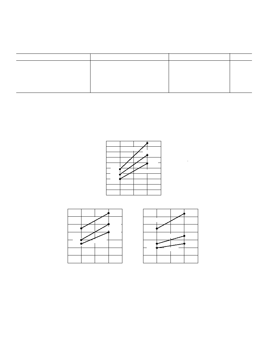
9mW
FREQUENCY MHz
2
6
4
8
0
IDD IDLE
1
8mW
6mW
5mW
POWER mW
10mW
13mW
10
12
14
5.00
7.00
10.00
15.00
13.83
V
DD
= 3.6V
V
DD
= 3.30V
V
DD
= 3.0V
FREQUENCY MHz
50
40
5.00
45
15
IDD DYNAMIC
1,2
V
DD
= 3.6V
V
DD
= 3.30V
V
DD
= 3.0V
48mW
37mW
29mW
24mW
19mW
15mW
POWER mW
35
30
25
20
7.00
10.00
13.83
15.00
10
5
0
IDD IDLE
n MODES
3
13mW
7mW
6mW
9mW
5mW
4mW
POWER mW
IDLE 16
IDLE 128
IDD IDLE
2
6
4
8
0
10
12
14
FREQUENCY MHz
5.00
7.00
10.00
15.00
13.83
VALID FOR ALL TEMPERATURE GRADES.
1
POWER REFLECTS DEVICE OPERATING WITH NO OUTPUT LOADS.
2
IDLE REFERS TO ADSP-216x OPERATION DURING EXECUTION OF IDLE INSTRUCTION.
DEASSERTED PINS ARE DRIVEN TO EITHER V
DD
OR GND.
3
MAXIMUM POWER DISSIPATION AT V
DD
= 3.6V DURING EXECUTION OF
IDLE n INSTRUCTION.
Figure 15. ADSP-2162 Power (Typical) vs. Frequency)
REV. 0
ADSP-216x
19
POWER DISSIPATION EXAMPLE
To determine total power dissipation in a specific application,
the following equation should be applied for each output:
C
×
V
DD
2
×
f
C = load capacitance, f = output switching frequency.
Example:
In an ADSP-2162 application where external data memory is
used and no other outputs are active, power dissipation is calcu-
lated as follows:
Assumptions:
· External data memory is accessed every cycle with 50% of the
address pins switching.
· External data memory writes occur every other cycle with
50% of the data pins switching.
· Each address and data pin has a 10 pF total load at the pin.
· The application operates at V
DD
= 3.3 V and t
CK
= 100 ns.
Total Power Dissipation = P
INT
+ (C
×
V
DD
2
×
f)
P
INT
= internal power dissipation (from Figure 15).
(C
×
V
DD
2
×
f) is calculated for each output:
# of
Output
Pins
C
V
DD
2
f
Address,
DMS 8
×
10 pF
×
3.3
2
V
×
10 MHz = 8.71 mW
Data,
WR
9
×
10 pF
×
3.3
2
V
×
5 MHz
= 4.90 mW
RD
1
×
10 pF
×
3.3
2
V
×
5 MHz
= 0.55 mW
CLKOUT
1
×
10 pF
×
3.3
2
V
×
10 MHz = 1.09 mW
15.25 mW
Total power dissipation for this example = P
INT
+ 15.25 mW.
ENVIRONMENTAL CONDITIONS
Ambient Temperature Rating:
T
AMB
= T
CASE
(PD
×
CA
)
T
CASE
= Case Temperature in
°
C
PD = Power Dissipation in W
CA
= Thermal Resistance (Case-to-Ambient)
JA
= Thermal Resistance (Junction-to-Ambient)
JC
= Thermal Resistance (Junction-to-Case)
Package
JA
JC
CA
MQFP
60
°
C/W
18
°
C/W
42
°
C/W
ADSP-2162/ADSP-2164/ADSP-2166
CAPACITIVE LOADING
Figures 16 and 17 show capacitive loading characteristics for
the ADSP-2162 and ADSP-2164.
C
L
pF
RISE TIME (0.4V 2.0V) ns
0
0
175
25
50
150
5
V
DD
= 3.0V
30
20
100
125
75
35
25
15
10
Figure 16. Typical Output Rise Time vs. Load Capaci-
tance, C
L
(at Maximum Ambient Operating Temperature)
C
L
pF
RISE TIME (0.4V 2.0V) ns
4
0
175
25
50
150
V
DD
= 3.0V
100
125
75
2
NOMINAL
2
4
6
8
10
Figure 17. Typical Output Valid Delay or Hold vs. Load
Capacitance, C
L
(at Maximum Ambient Operating
Temperature)
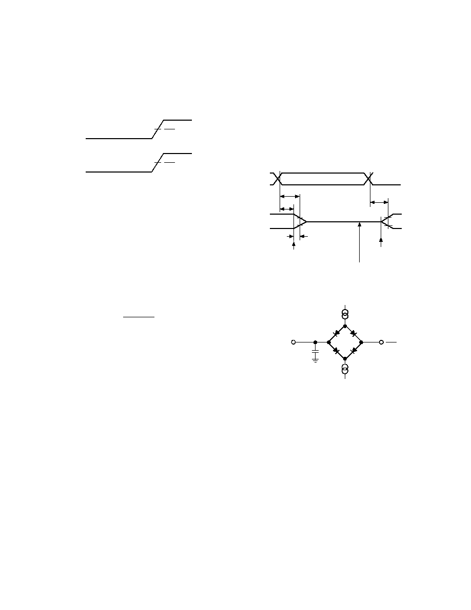
REV. 0
ADSP-216x
20
SPECIFICATIONS
ADSP-2162/ADSP-2164/ADSP-2166
TEST CONDITIONS
Figure 18 shows voltage reference levels for ac measurements.
V
DD
2
OUTPUT
INPUT
V
DD
2
Figure 18. Voltage Reference Levels for AC Measurements
(Except Output Enable/Disable)
Output Disable Time
Output pins are considered to be disabled when they have
stopped driving and started a transition from the measured
output high or low voltage to a high impedance state. The out-
put disable time (t
DIS
) is the difference of t
MEASURED
and t
DECAY
,
as shown in Figure 19. The time t
MEASURED
is the interval from
when a reference signal reaches a high or low voltage level to
when the output voltages have changed by 0.5 V from the mea-
sured output high or low voltage.
The decay time, t
DECAY
, is dependent on the capacitative load,
C
L
, and the current load, i
L
, on the output pin. It can be ap-
proximated by the following equation:
t
C
V
i
DECAY
L
L
=
×
0 5
.
from which
t
DIS
= t
MEASURED
t
DECAY
is calculated. If multiple pins (such as the data bus) are disabled,
the measurement value is that of the last pin to stop driving.
Output Enable Time
Output pins are considered to be enabled when they have made
a transition from a high-impedance state to when they start
driving. The output enable time (t
ENA
) is the interval from when
a reference signal reaches a high or low voltage level to when the
output has reached a specified high or low trip point, as shown
in Figure 19. If multiple pins (such as the data bus) are enabled,
the measurement value is that of the first pin to start driving.
2.0V
1.0V
t
ENA
REFERENCE
SIGNAL
OUTPUT
t
DECAY
V
OH
(MEASURED)
OUTPUT STOPS
DRIVING
OUTPUT STARTS
DRIVING
t
DIS
t
MEASURED
V
OL
(MEASURED)
V
OH
(MEASURED) 0.5V
V
OL
(MEASURED) +0.5V
HIGH-IMPEDANCE STATE. TEST CONDITIONS CAUSE
THIS VOLTAGE LEVEL TO BE APPROXIMATELY 1.5V.
V
OH
(MEASURED)
V
OL
(MEASURED)
Figure 19. Output Enable/Disable
TO
OUTPUT
PIN
50pF
I
OH
I
OL
V
DD
2
Figure 20. Equivalent Device Loading for AC
Measurements (Except Output Enable/Disable)

REV. 0
ADSP-216x
21
TIMING PARAMETERS (ADSP-2161/ADSP-2163/ADSP-2165)
GENERAL NOTES
Use the exact timing information given. Do not attempt to de-
rive parameters from the addition or subtraction of others. While
addition or subtraction would yield meaningful results for an
individual device, the values given in this data sheet reflect sta-
tistical variations and worst cases. Consequently, you cannot
meaningfully add parameters to derive longer times.
TIMING NOTES
Switching Characteristics specify how the processor changes its
signals. You have no control over this timing--circuitry external
to the processor must be designed for compatibility with these
signal characteristics. Switching characteristics tell you what the
processor will do in a given circumstance. You can also use
switching characteristics to ensure that any timing requirement
of a device connected to the processor (such as memory) is
satisfied.
Timing Requirements apply to signals that are controlled by cir-
cuitry external to the processor, such as the data input for a read
operation. Timing requirements guarantee that the processor
operates correctly with other devices.
MEMORY REQUIREMENTS
The table below shows common memory device specifications
and the corresponding ADSP-216x timing parameters, for your
convenience.
ADSP-216x
Memory Device Specification
Timing Parameter
Timing Parameter Definition
Address Setup to Write Start
t
ASW
A0A13,
DMS, PMS Setup Before WR Low
Address Setup to Write End
t
AW
A0A13,
DMS, PMS Setup Before WR Deasserted
Address Hold Time
t
WRA
A0A13,
DMS, PMS Hold After WR Deasserted
Data Setup Time
t
DW
Data Setup Before
WR High
Data Hold Time
t
DH
Data Hold After
WR High
OE to Data Valid
t
RDD
RD Low to Data Valid
Address Access Time
t
AA
A0A13,
DMS, PMS, BMS to Data Valid
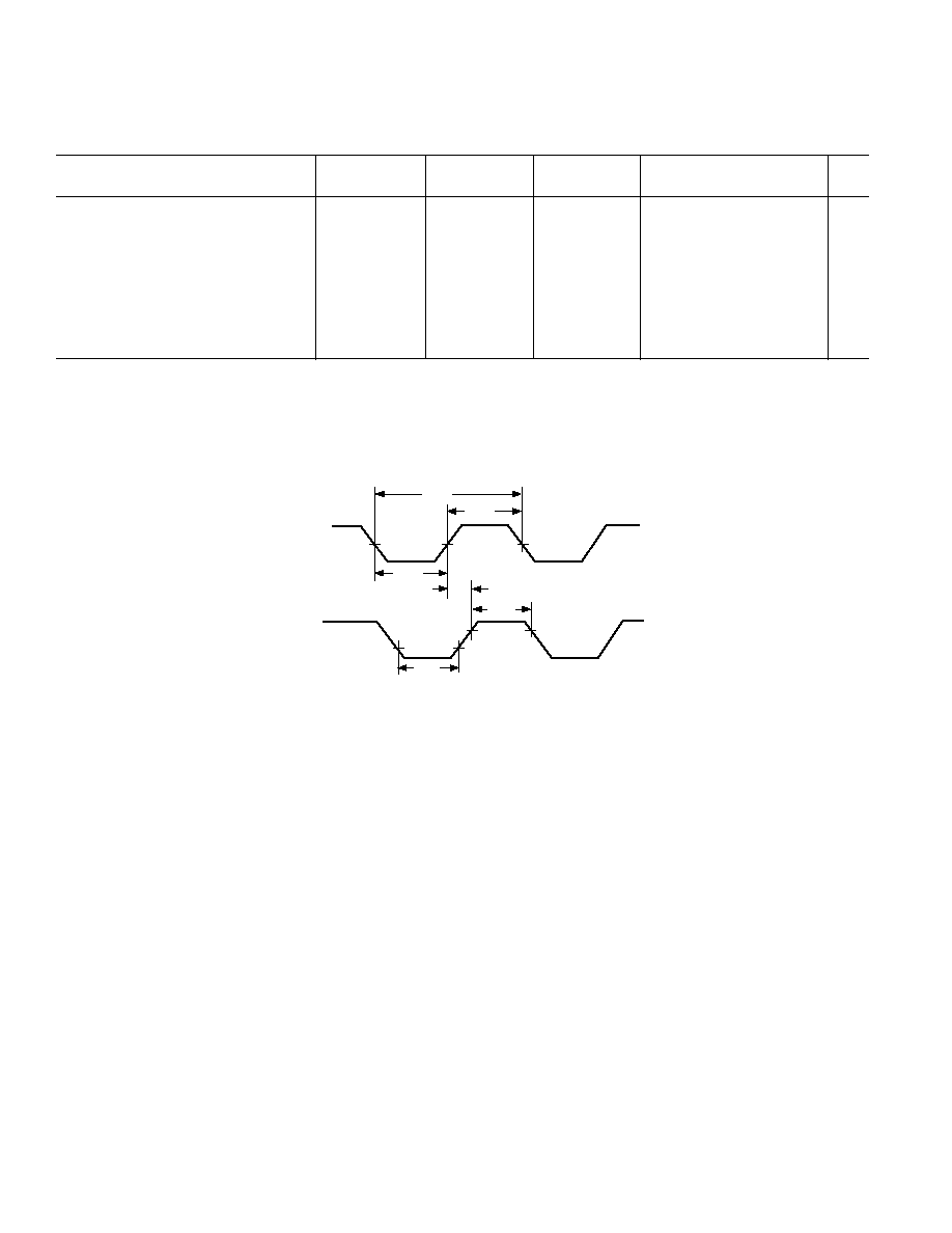
REV. 0
ADSP-216x
22
TIMING PARAMETERS (ADSP-2161/ADSP-2163/ADSP-2165)
CLOCK SIGNALS AND RESET
16.67 MHz
20 MHz
25 MHz
Frequency Dependency
Parameter
Min
Max
Min
Max
Min
Max
Min
Max
Unit
Timing Requirements:
t
CK
CLKIN Period
60
150
50
150
40
150
t
CK
150
ns
t
CKL
CLKIN Width Low
20
20
15
20
ns
t
CKH
CLKIN Width High
20
20
15
20
ns
t
RSP
RESET Width Low
300
250
200
5t
CK
1
ns
Switching Characteristics:
t
CPL
CLKOUT Width Low
20
15
10
0.5t
CK
10
ns
t
CPH
CLKOUT Width High
20
15
10
0.5t
CK
10
ns
t
CKOH
CLKIN High to CLKOUT High
0
20
0
20
0
15
2
0
20
2
ns
NOTES
1
Applies after power-up sequence is complete. Internal phase lock loop requires no more than 2000 CLKIN cycles, assuming stable CLKIN (not including crystal
oscillator startup time).
2
For 25 MHz only, the maximum frequency dependency for t
CKOH
= 15 ns.
CLKOUT
CLKIN
t
CPL
t
CHOK
t
CKL
t
CKH
t
CK
t
CPH
Figure 21. Clock Signals
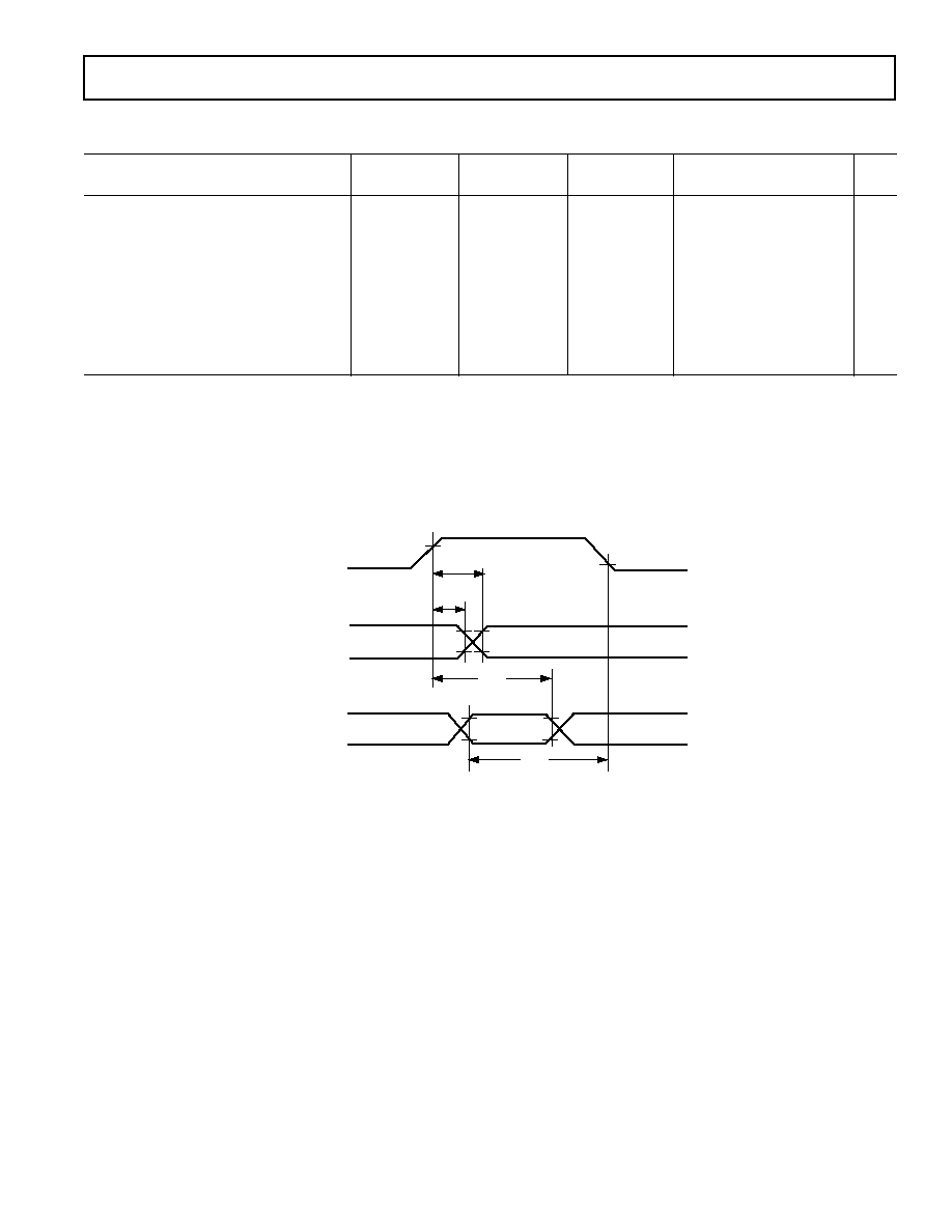
REV. 0
ADSP-216x
23
TIMING PARAMETERS (ADSP-2161/ADSP-2163/ADSP-2165)
INTERRUPTS AND FLAGS
16.67 MHz
20 MHz
25 MHz
Frequency Dependency
Parameter
Min
Max
Min
Max
Min
Max
Min
Max
Unit
Timing Requirements:
t
IFS
IRQx
1
or FI Setup Before
30
27.5
25
0.25t
CK
+ 15
ns
CLKOUT Low
2, 3
t
IFS
IRQx
1
or FI Setup Before
33
30.5
28
0.25t
CK
+ 18
ns
CLKOUT Low
2, 3
t
IFH
IRQx
1
or FI Hold After CLKOUT
15
12.5
10
0.25t
CK
ns
High
2, 3
Switching Characteristics:
t
FOH
FO Hold After CLKOUT High
0
0
0
0
ns
t
FOD
FO Delay from CLKOUT High
15
15
12
4
15
4
ns
NOTES
1
IRQx = IRQ0, IRQ1, and IRQ2.
2
If
IRQx and FI inputs meet t
IFS
and t
IFH
setup/hold requirements, they will be recognized during the current clock cycle; otherwise they will be recognized during the
following cycle. (Refer to the "Interrupt Controller" section in Chapter 3, Program Control, of the ADSP-2100 Family User's Manual, Third Edition for further
information on interrupt servicing.)
3
Edge-sensitive interrupts require pulsewidths greater than 10 ns. Level-sensitive interrupts must be held low until serviced.
4
For 25 MHz only, the maximum frequency dependency for t
FOD
= 12 ns.
t
FOH
CLKOUT
FLAG
OUTPUT(S)
IRQx
FI
t
IFS
t
IFH
t
FOD
Figure 22. Interrupts and Flags
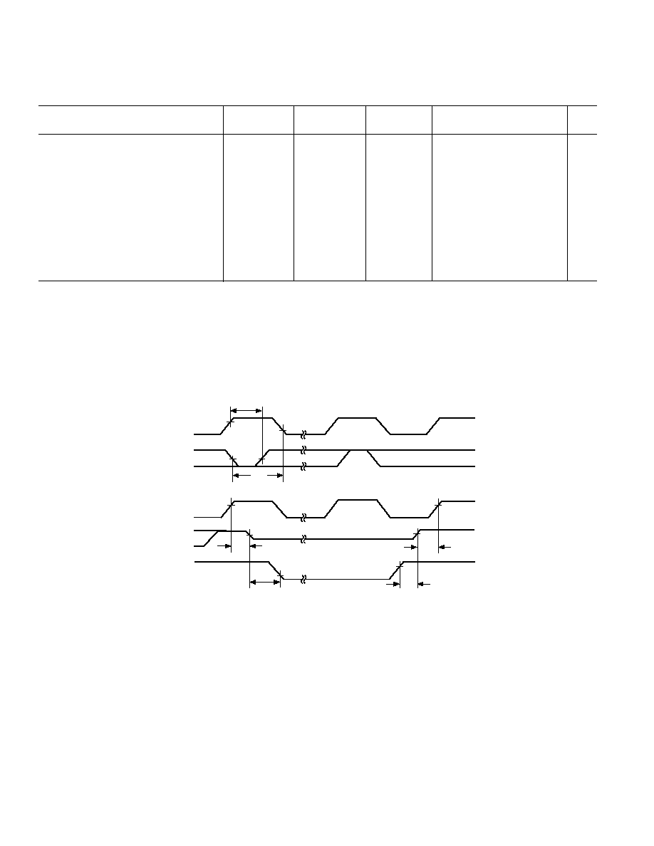
REV. 0
ADSP-216x
24
TIMING PARAMETERS (ADSP-2161/ADSP-2163/ADSP-2165)
BUS REQUEST/BUS GRANT
16.67 MHz
20 MHz
25 MHz
Frequency Dependency
Parameter
Min
Max
Min
Max
Min
Max
Min
Max
Unit
Timing Requirements:
t
BH
BR Hold After CLKOUT High
1
20
17.5
15
0.25t
CK
+ 5
ns
t
BS
BR Setup Before CLKOUT Low
1
35
32.5
30
0.25t
CK
+ 20
ns
Switching Characteristics:
t
SD
CLKOUT High to
DMS,
35
32.5
30
0.25t
CK
+ 20
ns
PMS, BMS, RD, WR Disable
t
SDB
DMS, PMS, BMS, RD, WR
0
0
0
0
ns
Disable to
BG Low
t
SE
BG High to DMS, PMS,
0
0
0
0
ns
BMS, RD, WR Enable
t
SEC
DMS, PMS, BMS, RD, WR
5
2.5
1.5
2
0.25t
CK
10
2
ns
Enable to CLKOUT High
NOTES
1
If
BR meets the t
BS
and t
BH
setup/hold requirements, it will be recognized in the current processor cycle; otherwise it is recognized in the following cycle.
BR requires
a pulsewidth greater than 10 ns.
2
For 25 MHz only, the minimum frequency dependency formula for t
SEC
= (0.25t
CK
8.5).
Section 10.2.4, "Bus Request/Grant," on page 212 of the ADSP-2100 Family User's Manual, Third Edition, states that "When
BR is recognized, the processor responds
immediately by asserting
BG during the same cycle." This is incorrect for the current versions of all ADSP-21xx processors: BG is asserted in the cycle after BR is
recognized. No external synchronization circuit is needed when
BR is generated as an asynchronous signal.
CLKOUT
t
SD
t
SDB
t
SE
t
SEC
t
BS
BR
t
BH
CLKOUT
PMS
,
DMS
BMS
,
RD
WR
BG
Figure 23. Bus Request/Bus Grant
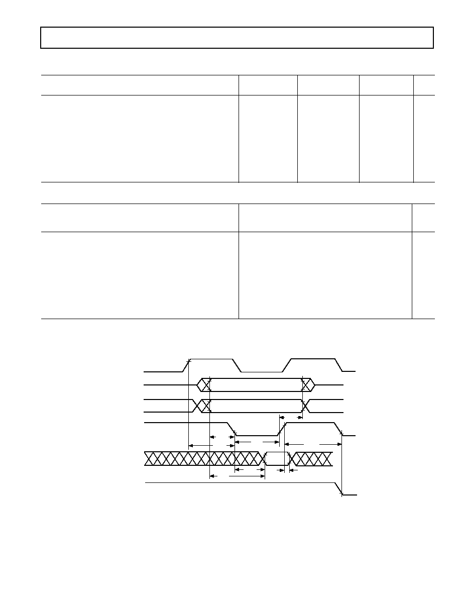
REV. 0
ADSP-216x
25
TIMING PARAMETERS (ADSP-2161/ADSP-2163/ADSP-2165)
MEMORY READ
16.67 MHz
20 MHz
25 MHz
Parameter
Min
Max
Min
Max
Min
Max
Unit
Timing Requirements:
t
RDD
RD Low to Data Valid
17
12
7
ns
t
AA
A0A13,
PMS, DMS, BMS to Data Valid
27
19.5
12
ns
t
RDH
Data Hold from
RD High
0
0
0
ns
Switching Characteristics:
t
RP
RD Pulsewidth
22
17
12
ns
t
CRD
CLKOUT High to
RD Low
10
25
7.5
22.5
5
20
ns
t
ASR
A0A13,
PMS, DMS, BMS Setup Before RD Low
5
2.5
1.5
1
ns
t
RDA
A0A13,
PMS, DMS, BMS Hold After RD Deasserted
6
3.5
1
ns
t
RWR
RD High to RD or WR Low
25
20
15
ns
Frequency Dependency
(CLKIN
25 MHz)
Parameter
Min
Max
Unit
Timing Requirements:
t
RDD
RD Low to Data Valid
0.5t
CK
13 + w
ns
t
AA
A0A13,
PMS, DMS, BMS to Data Valid
0.75t
CK
18 + w
ns
t
RDH
Data Hold from
RD High
0
Switching Characteristics:
t
RP
RD Pulsewidth
0.5t
CK
8 + w
ns
t
CRD
CLKOUT High to
RD Low
0.25t
CK
5
0.25t
CK
+ 10
ns
t
ASR
A0A13,
PMS, DMS, BMS Setup Before RD Low
0.25t
CK
10
1
ns
t
RDA
A0A13,
PMS, DMS, BMS Hold After RD Deasserted
0.25t
CK
9
ns
t
RWR
RD High to RD or WR Low
0.5t
CK
5
ns
NOTES
1
For 25 MHz only, minimum frequency dependency formula for t
ASR
= (0.25t
CK
8.5).
w = wait states
×
t
CK.
CLKOUT
A0A13
D
t
RDA
t
RWR
t
RP
t
ASR
t
CRD
t
RDD
t
AA
t
RDH
DMS
,
PMS
,
BMS
RD
WR
Figure 24. Memory Read
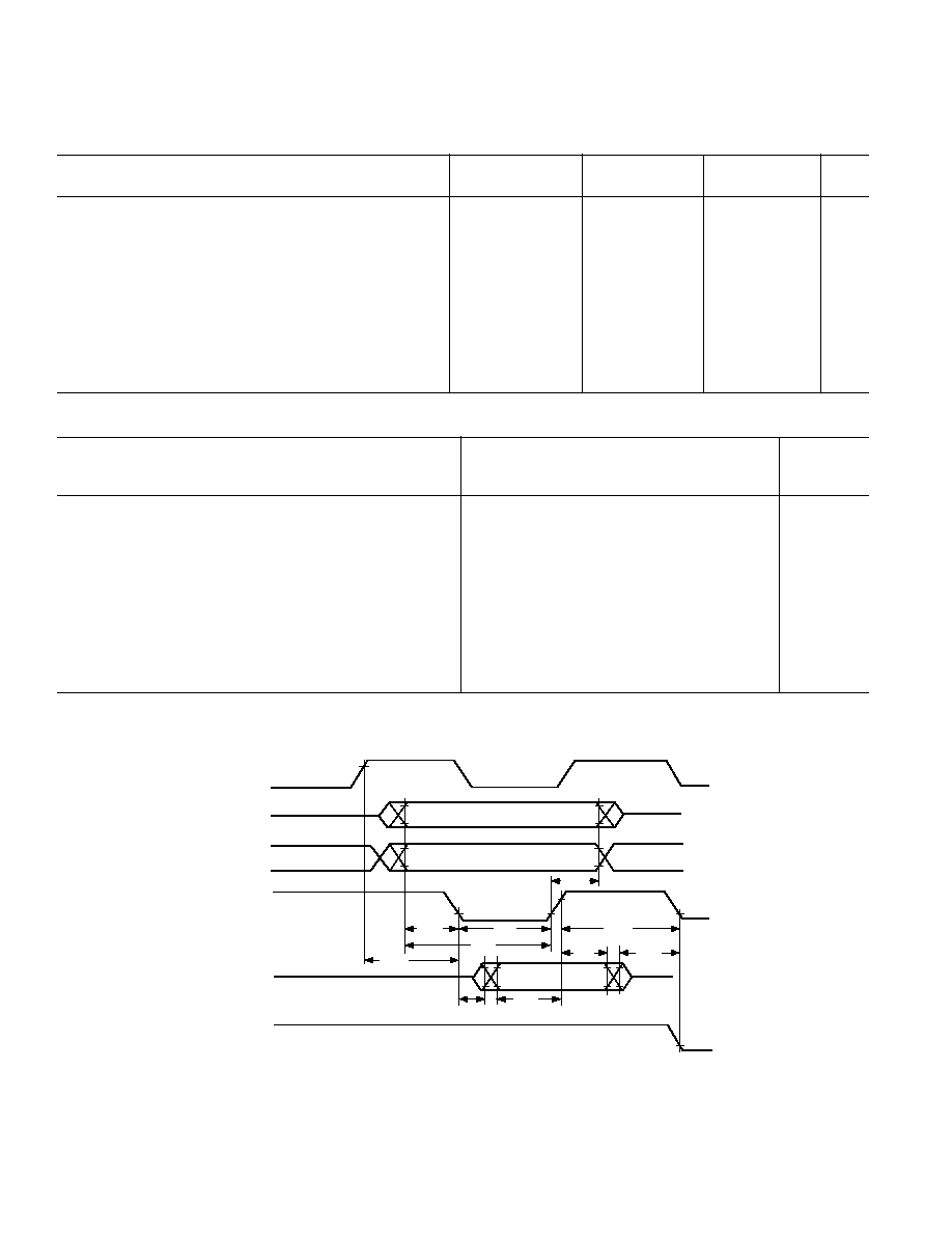
REV. 0
ADSP-216x
26
TIMING PARAMETERS (ADSP-2161/ADSP-2163/ADSP-2165)
MEMORY WRITE
16.67 MHz
20 MHz
25 MHz
Parameter
Min
Max
Min
Max
Min
Max
Unit
Switching Characteristics:
t
DW
Data Setup Before
WR High
17
12
7
ns
t
DH
Data Hold After
WR High
5
2.5
0
ns
t
WP
WR Pulsewidth
22
17
12
ns
t
WDE
WR Low to Data Enabled
0
0
0
ns
t
ASW
A0A13,
DMS, PMS Setup Before WR Low
5
2.5
1.5
1
ns
t
DDR
Data Disable Before
WR or RD Low
5
2.5
1.5
1
ns
t
CWR
CLKOUT High to
WR Low
10
25
7.5
22.5
5
20
ns
t
AW
A0A13,
DMS, PMS, Setup Before WR Deasserted
23
15.5
8
ns
t
WRA
A0A13,
DMS, PMS Hold After WR Deasserted
6
3.5
1
ns
t
WWR
WR High to RD or WR Low
25
20
15
ns
Frequency Dependency
(CLKIN
25 MHz)
Parameter
Min
Max
Unit
Switching Characteristics:
t
DW
Data Setup Before
WR High
0.5t
CK
13 + w
ns
t
DH
Data Hold After
WR High
0.25t
CK
10
ns
t
WP
WR Pulsewidth
0.5t
CK
8 + w
ns
t
WDE
WR Low to Data Enabled
0
t
ASW
A0A13,
DMS, PMS Setup Before WR Low
0.25t
CK
10
1
ns
t
DDR
Data Disable Before
WR or RD Low
0.25t
CK
10
1
ns
t
CWR
CLKOUT High to
WR Low
0.25t
CK
5
0.25t
CK
+ 10
ns
t
AW
A0A13,
DMS, PMS, Setup Before WR Deasserted
0.75t
CK
22 + w
ns
t
WRA
A0A13,
DMS, PMS Hold After WR Deasserted
0.25t
CK
9
ns
t
WWR
WR High to RD or WR Low
0.5t
CK
5
ns
NOTES
1
For 25 MHz only, the minimum frequency dependency formula for t
ASW
and t
DDR
= (0.25t
CK
8.5).
w = wait states
×
t
CK
.
CLKOUT
A0A13
D
t
WP
t
AW
t
CWR
t
DH
t
WDE
t
DW
t
ASW
t
WWR
t
WRA
t
DDR
DMS
,
PMS
,
BMS
RD
WR
Figure 25. Memory Write
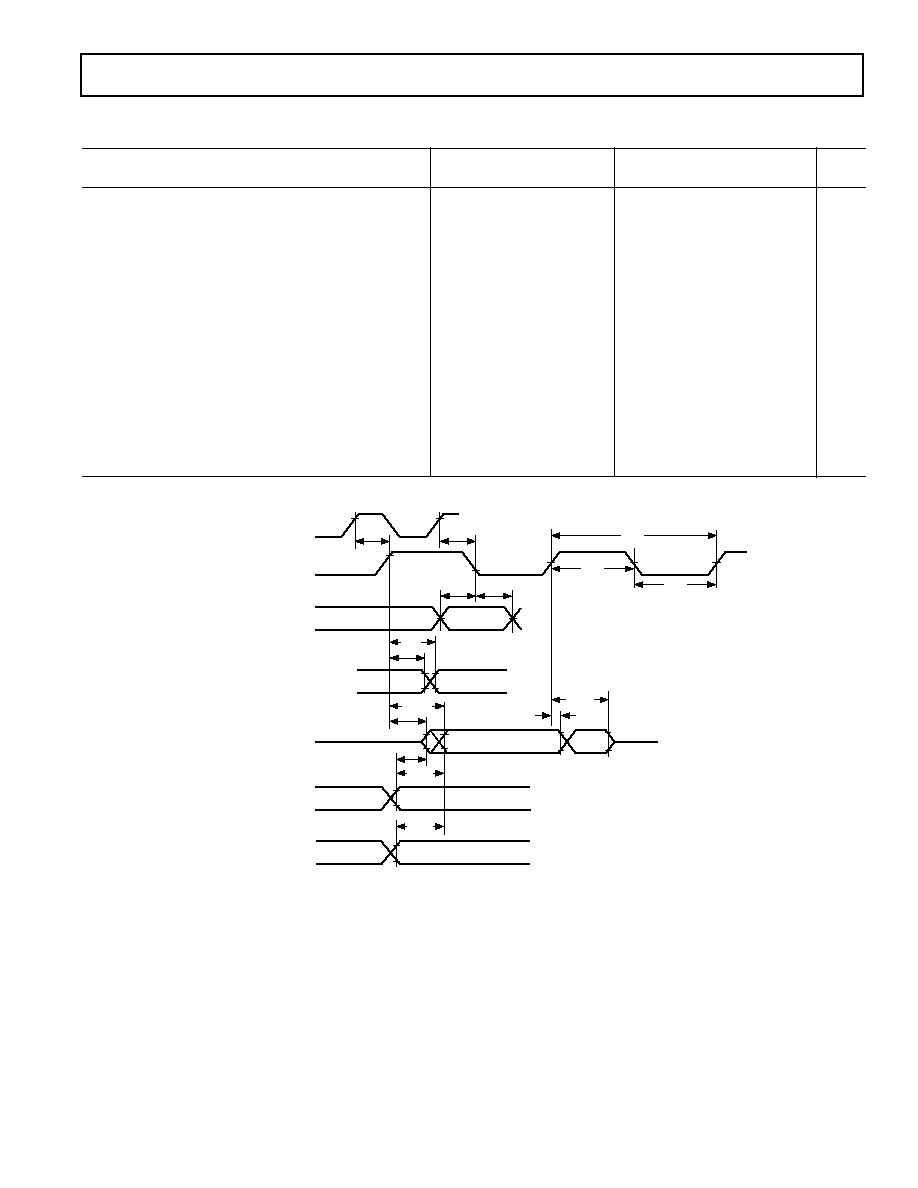
REV. 0
ADSP-216x
27
TIMING PARAMETERS (ADSP-2161/ADSP-2163/ADSP-2165)
SERIAL PORTS
13.824 MHz*
Frequency Dependency
Parameter
Min
Max
Min
Max
Unit
Timing Requirements:
t
SCK
SCLK Period
72.3
72.3
ns
t
SCS
DR/TFS/RFS Setup Before SCLK Low
8
8
ns
t
SCH
DR/TFS/RFS Hold After SCLK Low
10
10
ns
t
SCP
SCLK
IN
Width
28
28
ns
Switching Characteristics:
t
CC
CLKOUT High to SCLK
OUT
18.1
33.1
0.25t
CK
0.25t
CK
+ 15
ns
t
SCDE
SCLK High to DT Enable
0
0
ns
t
SCDV
SCLK High to DT Valid
20
20
ns
t
RH
TFS/RFS
OUT
Hold After SCLK High
0
0
ns
t
RD
TFS/RFS
OUT
Delay from SCLK High
20
20
ns
t
SCDH
DT Hold After SCLK High
0
0
ns
t
TDE
TFS (Alt) to DT Enable
0
0
ns
t
TDV
TFS (Alt) to DT Valid
18
18
ns
t
SCDD
SCLK High to DT Disable
25
25
ns
t
RDV
RFS (Multichannel, Frame Delay Zero)
20
20
ns
to DT Valid
*Maximum serial port operating frequency is 13.824 MHz for all processor speed grades.
CLKOUT
SCLK
TFS
DT
t
CC
t
CC
t
SCS
t
SCH
t
RH
t
SCDE
t
SCDH
t
SCDD
t
TDE
t
RDV
DR
TFS
IN
RFS
IN
RFS
OUT
TFS
OUT
t
TDV
t
SCDV
t
RD
t
SCP
t
SCK
t
SCP
(ALTERNATE
FRAME MODE)
RFS
(MULTICHANNEL MODE,
FRAME DELAY 0 {MFD = 0})
Figure 26. Serial Ports

REV. 0
ADSP-216x
28
TIMING PARAMETERS (ADSP-2162/ADSP-2164/ADSP-2166)
GENERAL NOTES
Use the exact timing information given. Do not attempt to de-
rive parameters from the addition or subtraction of others. While
addition or subtraction would yield meaningful results for an
individual device, the values given in this data sheet reflect sta-
tistical variations and worst cases. Consequently, you cannot
meaningfully add parameters to derive longer times.
TIMING NOTES
Switching Characteristics specify how the processor changes its
signals. You have no control over this timing--circuitry external
to the processor must be designed for compatibility with these
signal characteristics. Switching characteristics tell you what the
processor will do in a given circumstance. You can also use
switching characteristics to ensure that any timing requirement
of a device connected to the processor (such as memory) is
satisfied.
Timing Requirements apply to signals that are controlled by cir-
cuitry external to the processor, such as the data input for a read
operation. Timing requirements guarantee that the processor
operates correctly with other devices.
MEMORY REQUIREMENTS
The table below shows common memory device specifications
and the corresponding ADSP-216x timing parameters, for your
convenience.
ADSP-216x
Memory Device Specification
Timing Parameter
Timing Parameter Definition
Address Setup to Write Start
t
ASW
A0A13,
DMS, PMS Setup Before WR Low
Address Setup to Write End
t
AW
A0A13,
DMS, PMS Setup Before WR Deasserted
Address Hold Time
t
WRA
A0A13,
DMS, PMS Hold After WR Deasserted
Data Setup Time
t
DW
Data Setup Before
WR High
Data Hold Time
t
DH
Data Hold After
WR High
OE to Data Valid
t
RDD
RD Low to Data Valid
Address Access Time
t
AA
A0A13,
DMS, PMS, BMS to Data Valid
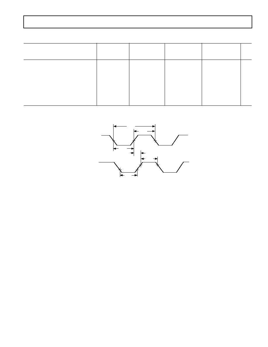
REV. 0
ADSP-216x
29
TIMING PARAMETERS (ADSP-2162/ADSP-2164/ADSP-2166)
CLOCK SIGNALS AND RESET
Frequency
10.24 MHz
13.0 MHz
16.67 MHz
Dependency
Parameter
Min
Max
Min
Max
Min
Max
Min
Max
Unit
Timing Requirements:
t
CK
CLKIN Period
97.6
150
76.9
150
60.0
150
t
CK
150
ns
t
CKL
CLKIN Width Low
20
20
20
20
ns
t
CKH
CLKIN Width High
20
20
20
20
ns
t
RSP
RESET Width Low
488
384.5
300
5t
CK
1
ns
Switching Characteristics:
t
CPL
CLKOUT Width Low
38.8
28.5
20
0.5t
CK
10
ns
t
CPH
CLKOUT Width High
38.8
28.5
20
0.5t
CK
10
ns
t
CKOH
CLKIN High to CLKOUT High
0
20
0
20
0
20
0
20
ns
NOTE
1
Applies after power-up sequence is complete. Internal phase lock loop requires no more than 2000 CLKIN cycles assuming stable CLKIN (not including crystal
oscillator startup time).
CLKOUT
CLKIN
t
CPL
t
CHOK
t
CKL
t
CKH
t
CK
t
CPH
Figure 27. Clock Signals
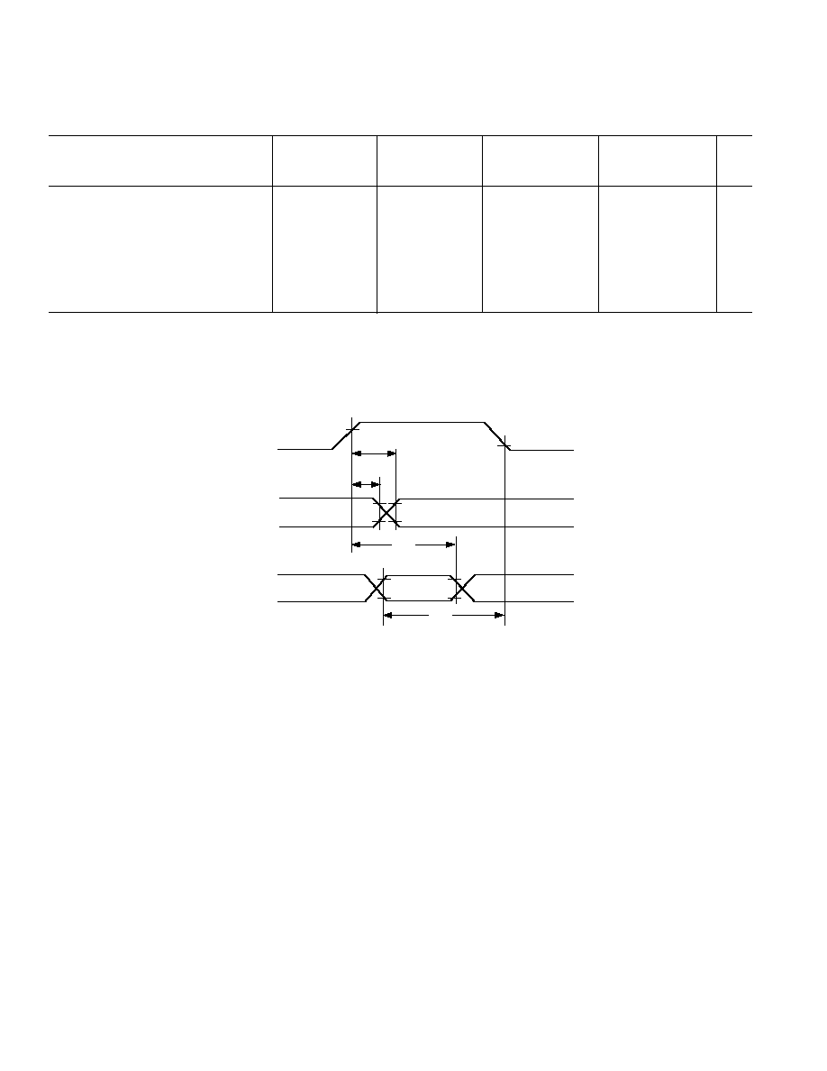
REV. 0
ADSP-216x
30
TIMING PARAMETERS (ADSP-2162/ADSP-2164/ADSP-2166)
INTERRUPTS AND FLAGS
Frequency
10.24 MHz
13.0 MHz
16.67 MHz
Dependency
Parameter
Min
Max
Min
Max
Min
Max
Min
Max
Unit
Timing Requirements:
t
IFS
IRQx
1
or FI Setup Before
CLKOUT Low
2, 3
44.4
39.2
35.0
0.25t
CK
+ 20
ns
t
IFH
IRQx
1
or FI Hold After
CLKOUT High
2, 3
24.4
19.2
15.0
0.25t
CK
ns
Switching Characteristics:
t
FOH
FO Hold After CLKOUT High
0
0
0
0
ns
t
FOD
FO Delay from CLKOUT High
15
15
15
15
ns
NOTES
1
IRQx = IRQ0, IRQ1, and IRQ2.
2
If
IRQx and FI inputs meet t
IFS
and t
IFH
setup/hold requirements, they will be recognized during the current clock cycle; otherwise they will be recognized during the
following cycle. (Refer to the "Interrupt Controller" section in Chapter 3, Program Control, of the ADSP-2100 Family User's Manual, Third Edition, for further
information on interrupt servicing.)
3
Edge-sensitive interrupts require pulse widths greater than 10 ns. Level-sensitive interrupts must be held low until serviced.
t
FOH
CLKOUT
FLAG
OUTPUT(S)
IRQx
FI
t
IFS
t
IFH
t
FOD
Figure 28. Interrupts and Flags
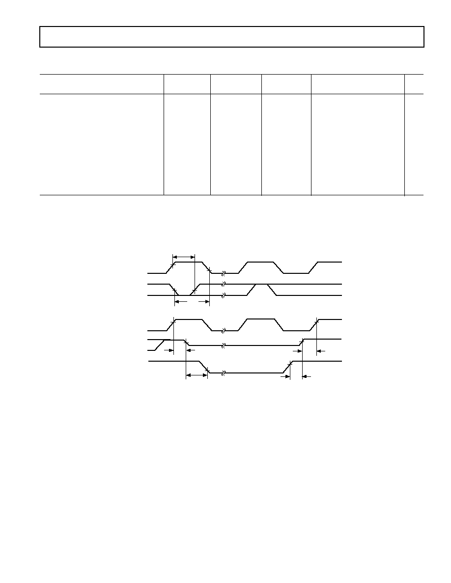
REV. 0
ADSP-216x
31
TIMING PARAMETERS (ADSP-2162/ADSP-2164/ADSP-2166)
BUS REQUEST/BUS GRANT
10.24 MHz
13.0 MHz
16.67 MHz
Frequency Dependency
Parameter
Min
Max
Min
Max
Min
Max
Min
Max
Unit
Timing Requirements:
t
BH
BR Hold After CLKOUT High
1
29.4
24.2
20.0
0.25t
CK
+ 5
ns
t
BS
BR Setup Before CLKOUT Low
1
44.4
39.2
35.0
0.25t
CK
+ 20
ns
Switching Characteristics:
t
SD
CLKOUT High to
DMS, PMS,
BMS, RD, WR Disable
44.4
39.2
35.0
0.25t
CK
+ 20
ns
t
SDB
DMS, PMS, BMS, RD, WR
Disable to
BG Low
0
0
0
0
ns
t
SE
BG High to DMS, PMS, BMS,
RD, WR Enable
0
0
0
0
ns
t
SEC
DMS, PMS, BMS, RD, WR
Enable to CLKOUT High
14.4
9.2
5.0
0.25t
CK
10
ns
NOTES
1
If
BR meets the t
BS
and t
BH
setup/hold requirements, it will be recognized in the current processor cycle; otherwise it is recognized in the following cycle.
BR
requires a pulsewidth greater than 10 ns.
Section 10.2.4, "Bus Request/Grant," of the ADSP-2100 Family User's Manual, Third Edition, states that, "When
BR is recognized, the processor responds immedi-
ately by asserting
BG during the same cycle." This is incorrect for the current versions of all ADSP-21xx processors: BG is asserted in the cycle after BR is recognized.
No external synchronization circuit is needed when
BR is generated as an asynchronous signal.
CLKOUT
t
SD
t
SDB
t
SE
t
SEC
t
BS
BR
t
BH
CLKOUT
PMS
,
DMS
BMS
,
RD
WR
BG
Figure 29. Bus Request/Grant
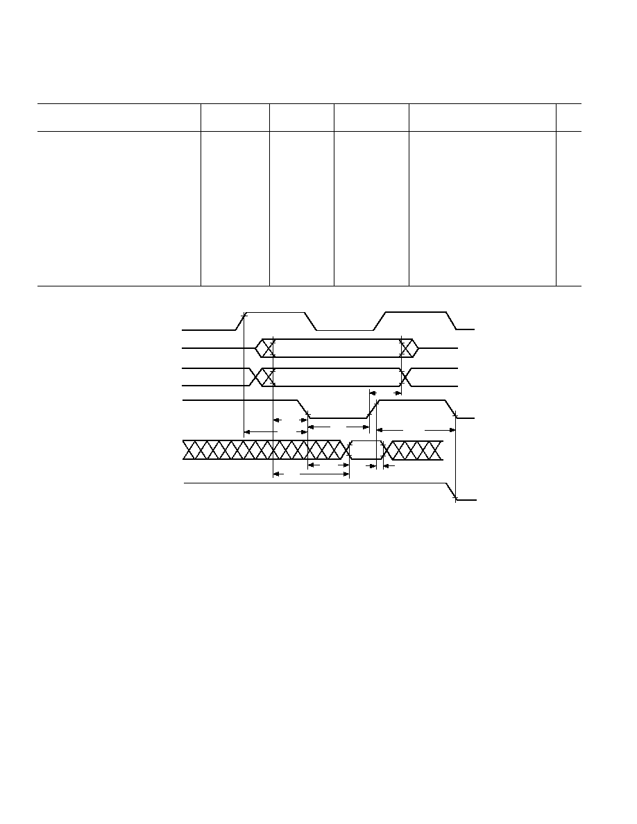
REV. 0
ADSP-216x
32
TIMING PARAMETERS (ADSP-2162/ADSP-2164/ADSP-2166)
MEMORY READ
10.24 MHz
13.0 MHz
16.67 MHz
Frequency Dependency
Parameter
Min
Max
Min
Max
Min
Max
Min
Max
Unit
Timing Requirements:
t
RDD
RD Low to Data Valid
33.8
23.5
15
0.5t
CK
15 + w
ns
t
AA
A0A13,
PMS, DMS, BMS to
Data Valid
49.2
33.7
21
0.75t
CK
24 + w
ns
t
RDH
Data Hold from
RD High
0
0
0
0
ns
Switching Characteristics:
t
RP
RD Pulsewidth
43.8
33.25
25
0.5t
CK
5 + w
ns
t
CRD
CLKOUT High to
RD Low
19.4
34.4
14.2
29.2
10.0
25.0
0.25t
CK
5
0.25t
CK
+ 10
ns
t
ASR
A0A13,
PMS, DMS, BMS
Setup Before
RD Low
12.4
7.2
3.0
0.25t
CK
12
ns
t
RDA
A0A13,
PMS, DMS, BMS
Hold After
RD Deasserted
14.4
9.2
5.0
0.25t
CK
10
ns
t
RWR
RD High to RD or WR Low
38.8
28.5
20.0
0.5t
CK
10
ns
w = wait states
×
t
CK.
CLKOUT
A0A13
D
t
RDA
t
RWR
t
RP
t
ASR
t
CRD
t
RDD
t
AA
t
RDH
DMS
,
PMS
,
BMS
RD
WR
Figure 30. Memory Read
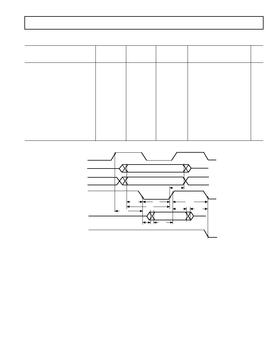
REV. 0
ADSP-216x
33
TIMING PARAMETERS (ADSP-2162/ADSP-2164/ADSP-2166)
MEMORY WRITE
Frequency
10.24 MHz
13.0 MHz
16.67 MHz
Dependency
Parameter
Min
Max
Min
Max
Min
Max
Min
Max
Unit
Switching Characteristics:
t
DW
Data Setup Before
WR High
38.8
28.25
20
0.5t
CK
10 + w
ns
t
DH
Data Hold After
WR High
14.4
9.2
5.0
0.25t
CK
10
ns
t
WP
WR Pulsewidth
43.8
33.25
25
0.5t
CK
5 + w
ns
t
WDE
WR Low to Data Enabled
0
0
0
0
t
ASW
A0A13,
DMS, DMS Setup
Before
WR Low
12.4
7.2
3.0
0.25t
CK
12
ns
t
DDR
Data Disable Before
WR
or
RD Low
14.4
9.2
5.0
0.25t
CK
10
ns
t
CWR
CLKOUT High to
WR Low
19.4
34.4
14.2
29.2
10.0
25.0
0.25t
CK
5
0.25t
CK
+ 10
ns
t
AW
A0A13,
DMS, PMS, Setup
Before
WR Deasserted
58.2
42.7
30
0.75t
CK
15 + w
ns
t
WRA
A0A13,
DMS, PMS Hold
After
WR Deasserted
14.4
9.2
5.0
0.25t
CK
10
ns
t
WWR
WR High to RD or WR Low
38.8
28.25
20
0.5t
CK
10
ns
w = wait states
×
t
CK.
CLKOUT
A0A13
D
t
WP
t
AW
t
CWR
t
DH
t
WDE
t
DW
t
ASW
t
WWR
t
WRA
t
DDR
DMS
,
PMS
,
BMS
RD
WR
Figure 31. Memory Write
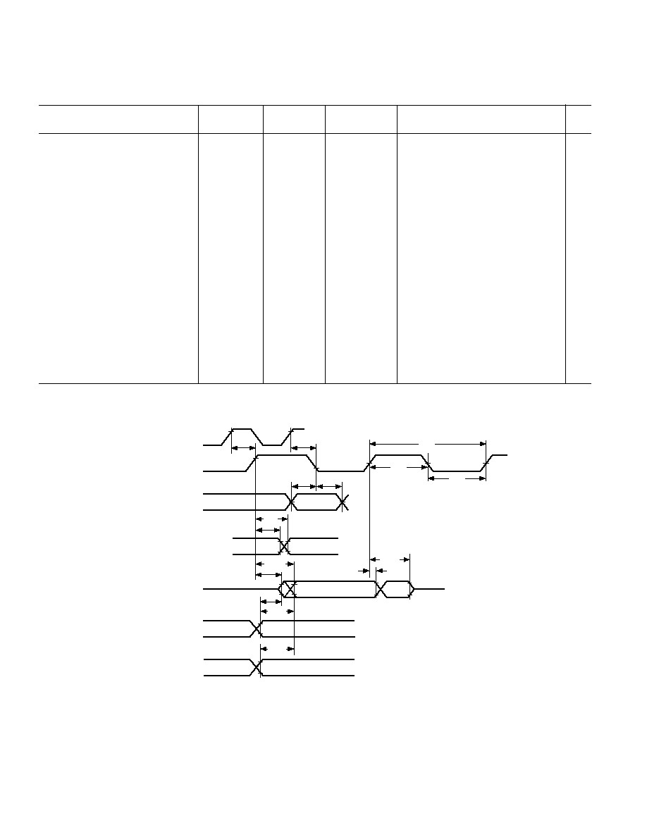
REV. 0
ADSP-216x
34
TIMING PARAMETERS (ADSP-2162/ADSP-2164/ADSP-2166)
SERIAL PORTS
10.24 MHz
13.0 MHz
13.824 MHz
1
Frequency Dependency
Parameter
Min
Max
Min
Max
Min
Max
Min
Max
Unit
Timing Requirements:
t
SCK
SCLK Period
97.6
76.9
72.3
1
t
CK
1
ns
t
SCS
DR/TFS/RFS Setup
Before SCLK Low
8
8
8
8
ns
t
SCH
DR/TFS/RFS Hold After
SCLK Low
10
10
10
10
ns
t
SCP
SCLK
IN
Width
28
28
28
28
ns
Switching Characteristics:
t
CC
CLKOUT High to SCLK
OUT
24.4
39.4
19.2
34.2
18.1
33.1
0.25t
CK
0.25t
CK
+ 15
ns
t
SCDE
SCLK High to DT Enable
0
0
0
0
ns
t
SCDV
SCLK High to DT Valid
28
2
20
20
20
2
ns
t
RH
TFS/RFS
OUT
Hold After
SCLK High
0
0
0
0
ns
t
RD
TFS/RFS
OUT
Delay from
SCLK High
28
2
20
20
20
2
ns
t
SCDH
DT Hold After SCLK High
0
0
0
0
ns
t
TDE
TFS (Alt) to DT Enable
0
0
0
0
ns
t
TDV
TFS (Alt) to DT Valid
18
18
18
18
ns
t
SCDD
SCLK High to DT Disable
30
2
25
25
25
2
ns
t
RDV
RFS (Multichannel, Frame 20
Delay Zero) to DT Valid
20
20
20
20
ns
NOTES
1
Maximum serial port operating frequency is 13.824 MHz for all processor speed grades faster then 13.824 MHz.
2
For 10.24 MHz only, the maximum frequency dependency for t
SCDV
= 28 ns, t
RD
= 28 ns, t
SCDD
= 30 ns.
CLKOUT
SCLK
TFS
DT
t
CC
t
CC
t
SCS
t
SCH
t
RH
t
SCDE
t
SCDH
t
SCDD
t
TDE
t
RDV
DR
TFS
IN
RFS
IN
RFS
OUT
TFS
OUT
t
TDV
t
SCDV
t
RD
t
SCP
t
SCK
t
SCP
(ALTERNATE
FRAME MODE)
RFS
(MULTICHANNEL MODE,
FRAME DELAY 0 {MFD = 0})
Figure 32. Serial Ports
REV. 0
ADSP-216x
35
PLCC
Pin
Number
Name
52
FO
(DT1)
53
IRQ1
(TFS1)
54
IRQ0
(RFS1)
55
FI
(DR1)
56
SCLK1
57
V
DD
58
D0
59
D1
60
D2
61
D3
62
D4
63
D5
64
D6
65
D7
66
D8
67
D9
68
D10
PLCC
Pin
Number
Name
1
D11
2
GND
3
D12
4
D13
5
D14
6
D15
7
D16
8
D17
9
D18
10
GND
11
D19
12
D20
13
D21
14
D22
15
D23
16
V
DD
17
MMAP
PLCC
Pin
Number
Name
18
BR
19
IRQ2
20
RESET
21
A0
22
A1
23
A2
24
A3
25
A4
26
V
DD
27
A5
28
A6
29
GND
30
A7
31
A8
32
A9
33
A10
34
A11
PLCC
Pin
Number
Name
35
A12
36
A13
37
PMS
38
DMS
39
BMS
40
BG
41
XTAL
42
CLKIN
43
CLKOUT
44
WR
45
RD
46
DT0
47
TFS0
48
RFS0
49
GND
50
DR0
51
SCLK0
PIN CONFIGURATIONS
68-Lead PLCC
10
11
12
13
14
15
16
17
18
19
20
22
23
24
25
26
21
27
43
28 29 30 31 32 33 34 35 36 37 38 39 40 41 42
9
61
8
7
6
5
68 67 66 65 64 63 62
4
3
2
1
60
59
58
57
56
55
54
53
52
51
50
49
48
47
46
45
44
PIN 1
IDENTIFIER
TOP VIEW
(Not to Scale)
D2
D1
D0
A9
A
6
A
7
A
8
A
1
0
A
1
1
D9
D6
D8
D7
D3
D10
D4
D5
D18
D15
D14
D13
D12
D17
D16
D11
GND
XTAL
C
L
K
I
N
CLKOUT
V
DD
SCLK1
FI
IRQ0
GND
D19
D20
D21
D22
D23
V
DD
MMAP
BR
IRQ2
RESET
IRQ1
FO
SCLK0
DR0
ADSP-216x
A0
A1
A2
A3
A4
V
DD
GND
RFS0
TFS0
DT0
RD
WR
A5
GND
A
1
2
A
1
3
BMS
BG
DMS
PMS
REV. 0
ADSP-216x
36
PIN CONFIGURATIONS
80-Lead MQFP
80
79
78
77
76
75
74
73
72
71
70
69
68
67
66
65
64
63
62
61
56
57
58
59
54
55
52
53
50
51
60
45
46
47
48
43
44
42
49
41
5
4
3
2
7
6
9
8
1
11
10
16
15
14
13
18
17
20
19
12
PIN 1
IDENTIFIER
TOP VIEW
(Not to Scale)
40
39
38
37
35
34
33
32
31
30
29
28
27
26
25
24
23
22
21
36
V
DD
A4
A3
A2
A1
A0
RESET
IRQ2
BR
MMAP
V
DD
D23
D22
D21
D20
D19
GND
GND
CLKOUT
WR
RD
DT0
TFS0
RFS0
GND
GND
DR0
SCLK0
FO
IRQ0
FI
SCLK1
V
DD
D0
D1
D2
D18
D17
D16
D15
D14
D13
D12
GND
GND
D11
D10
D9
D8
D6
D5
D4
NC
NC
NC
A5
A6
GND
GND
A7
A8
A9
A10
A11
A12
A13
PMS
DMS
BG
BMS
XTAL
CLKIN
*PWDACK
NC
D3
ADSP-216x
V
DD
IRQ1
*PWDFLAG
D7
V
DD
NC = NO CONNECT
MQFP
Pin
Number
Name
1
A5
2
A6
3
GND
4
GND
5
A7
6
A8
7
A9
8
A10
9
A11
10
A12
11
A13
12
PMS
13
DMS
14
BMS
15
BG
16
XTAL
17
CLKIN
18
PWDACK*
19
PWDFLAG*
20
NC
MQFP
Pin
Number
Name
21
CLKOUT
22
WR
23
RD
24
DT0
25
TFS0
26
RFS0
27
GND
28
GND
29
DR0
30
SCLK0
31
FO
(DT1)
32
IRQ1
(TFS1)
33
IRQ0
(RFS1)
34
FI
(DR1)
35
SCLK1
36
V
DD
37
D0
38
D1
39
D2
40
D3
MQFP
Pin
Number
Name
41
NC
42
NC
43
NC
44
D4
45
D5
46
D6
47
D7
48
D8
49
D9
50
D10
51
D11
52
GND
53
GND
54
D12
55
D13
56
D14
57
D15
58
D16
59
D17
60
D18
MQFP
Pin
Number
Name
61
GND
62
GND
63
D19
64
D20
65
D21
66
D22
67
D23
68
V
DD
69
V
DD
70
MMAP
71
BR
72
IRQ2
73
RESET
74
A0
75
A1
76
A2
77
A3
78
A4
79
V
DD
80
V
DD
*ADSP-2165/ADSP-2166 only.
Others "NC".
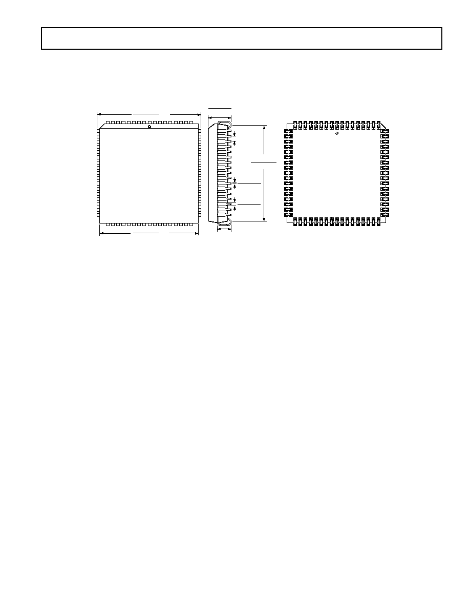
REV. 0
ADSP-216x
37
OUTLINE DIMENSIONS
ADSP-216x
68-Lead Plastic Leaded Chip Carrier (PLCC)
9
PIN 1
IDENTIFIER
10
61
60
26
27
44
43
TOP VIEW
(PINS DOWN)
0.995 (25.27)
0.985 (25.02)
SQ
0.954 (24.23)
0.950 (24.13)
SQ
0.019 (0.48)
0.017 (0.43)
0.050
(1.27)
TYP
0.925 (23.50)
0.895 (22.73)
0.029 (0.74)
0.027 (0.69)
0.104 (2.64) TYP
0.175 (4.45)
0.169 (4.29)
BOTTOM VIEW
(PINS UP)
PIN 1
IDENTIFIER
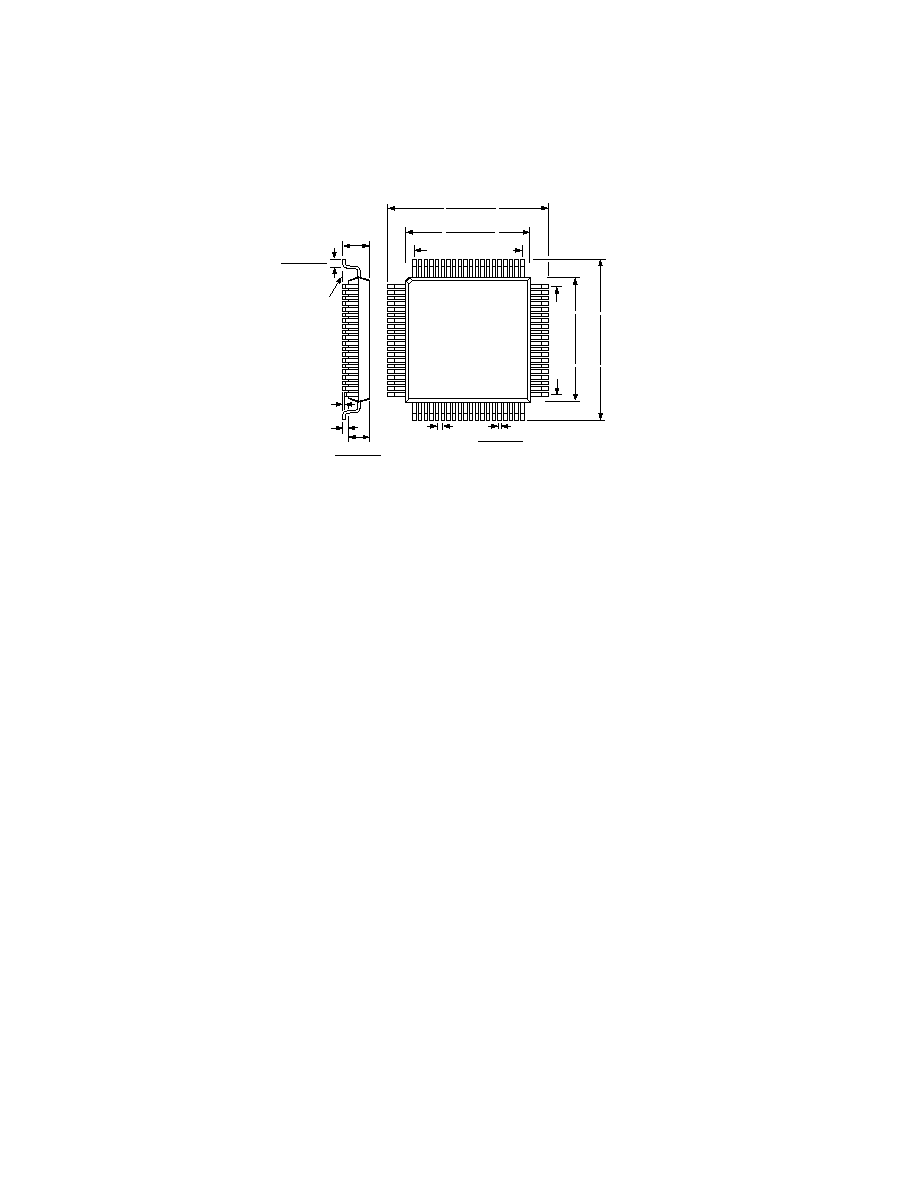
REV. 0
ADSP-216x
38
OUTLINE DIMENSIONS
ADSP-216x
80-Lead Plastic Quad Flatpack (MQFP)
SEATING
PLANE
0.134 (3.40)
MAX
0.041 (1.03)
0.031 (0.78)
0.004 (0.10)
MAX
0.120 (3.05)
0.100 (2.55)
0.010 (0.25)
MIN
0.014 (0.35)
0.010 (0.25)
0.690 (17.45)
0.667 (16.95)
0.555 (14.10)
0.547 (13.90)
0.555 (14.10)
0.547 (13.90)
0.690 (17.45
0.667 (16.95)
1
20
21
41
40
60
61
80
0.486 (12.35) BSC
0.486 (12.35) BSC
TOP VIEW
(PINS DOWN)
0.026 (0.65)
BSC
THE ACTUAL POSITION OF EACH LEAD
IS WITHIN 0.0047 (0.12) FROM ITS IDEAL
POSITION WHEN MEASURED IN THE
LATERAL DIRECTION.

REV. 0
ADSP-216x
39
ORDERING GUIDE
Ambient
Temperature
Instruction
Package
Package
Part Number
1
Range
Rate (MHz)
Description
Option
ADSP-2161KP-66
2
0
°
C to +70
°
C
16.67
68-Lead PLCC
P-68A
ADSP-2161BP-66
2
40
°
C to +85
°
C
16.67
68-Lead PLCC
P-68A
ADSP-2161KS-66
2
0
°
C to +70
°
C
16.67
80-Lead MQFP
S-80
ADSP-2161BS-66
2
40
°
C to +85
°
C
16.67
80-Lead MQFP
S-80
ADSP-2162KP-40 (3.3 V)
2
0
°
C to +70
°
C
10.24
68-Lead PLCC
P-68A
ADSP-2162BP-40 (3.3 V)
2
40
°
C to +85
°
C
10.24
68-Lead PLCC
P-68A
ADSP-2162KS-40 (3.3 V)
2
0
°
C to +70
°
C
10.24
80-Lead MQFP
S-80
ADSP-2163KP-66
2
0
°
C to +70
°
C
16.67
68-Lead PLCC
P-68A
ADSP-2163BP-66
2
40
°
C to +85
°
C
16.67
68-Lead PLCC
P-68A
ADSP-2163KS-66
2
0
°
C to +70
°
C
16.67
80-Lead MQFP
S-80
ADSP-2163BS-66
2
40
°
C to +85
°
C
16.67
80-Lead MQFP
S-80
ADSP-2163KP-100
2
0
°
C to +70
°
C
25
68-Lead PLCC
P-68A
ADSP-2163BP-100
2
40
°
C to +85
°
C
25
68-Lead PLCC
P-68A
ADSP-2163KS-100
2
0
°
C to +70
°
C
25
80-Lead MQFP
S-80
ADSP-2163BS-100
2
40
°
C to +85
°
C
25
80-Lead MQFP
S-80
ADSP-2164KP-40 (3.3 V)
2
0
°
C to +70
°
C
10.24
68-Lead PLCC
P-68A
ADSP-2164BP-40 (3.3 V)
2
40
°
C to +85
°
C
10.24
68-Lead PLCC
P-68A
ADSP-2164KS-40 (3.3 V)
2
0
°
C to +70
°
C
10.24
80-Lead MQFP
S-80
ADSP-2164BS-40 (3.3 V)
2
40
°
C to +85
°
C
10.24
80-Lead MQFP
S-80
ADSP-2165KS-80
0
°
C to +70
°
C
20.00
80-Lead MQFP
S-80
ADSP-2165KS-100
0
°
C to +70
°
C
25.00
80-Lead MQFP
S-80
ADSP-2165BS-80
40
°
C to +85
°
C
20.00
80-Lead MQFP
S-80
ADSP-2165BS-100
40
°
C to +85
°
C
25.00
80-Lead MQFP
S-80
ADSP-2166KS-52 (3.3 V)
0
°
C to +70
°
C
13.00
80-Lead MQFP
S-80
ADSP-2166KS-66 (3.3 V)
0
°
C to +70
°
C
16.67
80-Lead MQFP
S-80
ADSP-2166BS-52 (3.3 V)
40
°
C to +85
°
C
13.00
80-Lead MQFP
S-80
ADSP-2166BS-66 (3.3 V)
40
°
C to +85
°
C
16.67
80-Lead MQFP
S-80
NOTES
1
K = Commercial Temperature Range (0
°
C to +70
°
C).
B = Industrial Temperature Range (40
°
C to +85
°
C).
P = PLCC (Plastic Leaded Chip Carrier).
S = MQFP (Plastic Quad Flatpack).
2
Minimum order quantities required. Contact factory for further information.
3
Refer to the section titled "Ordering Procedure for ROM-Coded ADSP-216x Processors" for information about ROM coded parts.
C3511310/99
PRINTED IN U.S.A.