a
DSP Microcomputer
Information furnished by Analog Devices is believed to be accurate and reli-
able. However, no responsibility is assumed by Analog Devices for its use,
nor for any infringements of patents or other rights of third parties that may
result from its use. No license is granted by implication or otherwise under
any patent or patent rights of Analog Devices.
One Technology Way, P.O.Box 9106, Norwood, MA 02062-9106, U.S.A.
Tel:781/329-4700 http://www.analog.com
Fax:781/326-8703
© Analog Devices, Inc., 2001
REV. 0
ICE-Port is a trademark of Analog Devices, Inc.
ADSP-218xN Series
PERFORMANCE FEATURES
12.5 ns Instruction Cycle Time @1.8 V (Internal), 80 MIPS
Sustained Performance
Single-Cycle Instruction Execution
Single-Cycle Context Switch
3-Bus Architecture Allows Dual Operand Fetches in
Every Instruction Cycle
Multifunction Instructions
Power-Down Mode Featuring Low CMOS Standby
Power Dissipation with 200 CLKIN Cycle Recovery
from Power-Down Condition
Low Power Dissipation in Idle Mode
INTEGRATION FEATURES
ADSP-2100 Family Code Compatible (Easy to Use
Algebraic Syntax), with Instruction Set Extensions
Up to 256K Bytes of On-Chip RAM, Configured as
Up to 48K Words Program Memory RAM
Up to 56K Words Data Memory RAM
Dual-Purpose Program Memory for Both Instruction and
Data Storage
Independent ALU, Multiplier/Accumulator, and Barrel
Shifter Computational Units
Two Independent Data Address Generators
Powerful Program Sequencer Provides Zero Overhead
Looping Conditional Instruction Execution
Programmable 16-Bit Interval Timer with Prescaler
100-Lead LQFP and 144-Ball Mini-BGA
SYSTEM INTERFACE FEATURES
Flexible I/O Allows 1.8 V, 2.5 V or 3.3 V Operation
All Inputs Tolerate up to 3.6 V Regardless of Mode
16-Bit Internal DMA Port for High-Speed Access to On-
Chip Memory (Mode Selectable)
4M-Byte Memory Interface for Storage of Data Tables
and Program Overlays (Mode Selectable)
8-Bit DMA to Byte Memory for Transparent Program and
Data Memory Transfers (Mode Selectable)
Programmable Memory Strobe and Separate I/O
Memory Space Permits "Glueless" System Design
Programmable Wait State Generation
Two Double-Buffered Serial Ports with Companding
Hardware and Automatic Data Buffering
Automatic Booting of On-Chip Program Memory from
Byte-Wide External Memory, e.g., EPROM, or through
Internal DMA Port
Six External Interrupts
13 Programmable Flag Pins Provide Flexible System
Signaling
UART Emulation through Software SPORT
Reconfiguration
ICE-PortTM Emulator Interface Supports Debugging in
Final Systems
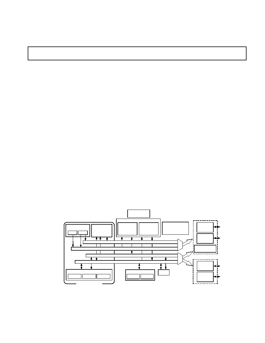
FUNCTIONAL BLOCK DIAGRAM
Ins
er
t c
hip
bl
oc
k d
iag
ra
m
he
re.
ARITHMETIC UNITS
SHIFTER
MAC
ALU
PROGRAM MEMORY ADDRESS
DATA MEMORY ADDRESS
PROGRAM MEMORY DATA
DATA MEMORY DATA
POWER-DOWN
CONTROL
MEMORY
PROGRAM
MEMORY
UP TO
48K 24-BIT
EXTERNAL
ADDRESS
BUS
EXTERNAL
DATA
BUS
BYTE DMA
CONTROLLER
SPORT0
SERIAL PORTS
SPORT1
PROGRAMMABLE
I/O
AND
FLAGS
TIMER
HOST MODE
OR
EXTERNAL
DATA
BUS
INTERNAL
DMA
PORT
DAG1
DATA ADDRESS
GENERATORS
DAG2
PROGRAM
SEQUENCER
ADSP-2100 BASE
ARCHITECTURE
DATA
MEMORY
UP TO
56K
16-BIT
FULL MEMORY MODE

ADSP-218xN Series
≠2≠
REV. 0
VisualDSP++ and EZ-KIT Lite are trademarks of Analog Devices, Inc.
GENERAL DESCRIPTION
The ADSP-218xN series consists of six single chip micro-
computers optimized for digital signal processing applica-
tions. The high-level block diagram for the ADSP-218xN
series members appears on the previous page. All series
members are pin-compatible and are differentiated solely by
the amount of on-chip SRAM. This feature, combined with
ADSP-21xx code compatibility, provides a great deal of
flexibility in the design decision. Specific family members
are shown in
Table 1
.
ADSP-218xN series members combine the ADSP-2100
family base architecture (three computational units, data
address generators, and a program sequencer) with two
serial ports, a 16-bit internal DMA port, a byte DMA port,
a programmable timer, Flag I/O, extensive interrupt capa-
bilities, and on-chip program and data memory.
ADSP-218xN series members integrate up to 256K bytes
of on-chip memory configured as up to 48K words (24-bit)
of program RAM, and up to 56K words (16-bit) of data
RAM. Power-down circuitry is also provided to meet the
low power needs of battery-operated portable equipment.
The ADSP-218xN is available in a 100-lead LQFP package
and 144-Ball Mini-BGA.
Fabricated in a high-speed, low-power, 0.18 Ķm CMOS
process, ADSP-218xN series members operate with a
12.5 ns instruction cycle time. Every instruction can
execute in a single processor cycle.
The ADSP-218xN's flexible architecture and comprehen-
sive instruction set allow the processor to perform multiple
operations in parallel. In one processor cycle, ADSP-218xN
series members can:
∑ Generate the next program address
∑ Fetch the next instruction
∑ Perform one or two data moves
∑ Update one or two data address pointers
∑ Perform a computational operation
This takes place while the processor continues to:
∑ Receive and transmit data through the two serial ports
∑ Receive and/or transmit data through the
internal DMA port
∑ Receive and/or transmit data through the byte DMA port
∑ Decrement timer
DEVELOPMENT SYSTEM
Analog Devices' wide range of software and hardware
development tools supports the ADSP-218xN series. The
DSP tools include an integrated development environment,
an evaluation kit, and a serial port emulator.
VisualDSP++TM is an integrated development environment,
allowing for fast and easy development, debug, and deploy-
ment. The VisualDSP++ project management environment
lets programmers develop and debug an application. This
environment includes an easy-to-use assembler that is based
on an algebraic syntax; an archiver (librarian/library build-
er); a linker; a PROM-splitter utility; a cycle-accurate,
instruction-level simulator; a C compiler; and a C run-time
library that
includes DSP and mathematical functions.
Debugging both C and assembly programs with the
VisualDSP++ debugger, programmers can:
∑ View mixed C and assembly code (interleaved source and
object information)
∑ Insert break points
∑ Set conditional breakpoints on registers, memory, and
stacks
∑ Trace instruction execution
∑ Fill and dump memory
∑ Source level debugging
The VisualDSP++ IDE lets programmers define and
manage DSP software development. The dialog boxes and
property pages let programmers configure and manage all
of the ADSP-218xN development tools, including the
syntax highlighting in the VisualDSP++ editor. This capa-
bility controls how the development tools process inputs and
generate outputs.
The ADSP-2189M EZ-KIT LiteTM provides developers
with a cost-effective method for initial evaluation of the
powerful ADSP-218xN DSP family architecture. The
ADSP-2189M EZ-KIT Lite includes a stand-alone ADSP-
2189M DSP board supported by an evaluation suite of
VisualDSP++. With this EZ-KIT Lite, users can learn
about DSP hardware and software development and evalu-
ate potential applications of the ADSP-218xN series. The
ADSP-2189M EZ-KIT Lite provides an evaluation suite of
the VisualDSP++ development environment with the
C compiler, assembler, and linker. The size of the DSP
erxecutable that can be built using the EZ-KIT Lite tools is
limited to 8K words.
Table 1. ADSP-218xN DSP Microcomputer Family
Device
Program
Memory
(K Words)
Data Memory
(K Words)
ADSP-2184N
4
4
ADSP-2185N
16
16
ADSP-2186N
8
8
ADSP-2187N
32
32
ADSP-2188N
48
56
ADSP-2189N
32
48

≠3≠
REV. 0
ADSP-218xN Series
The EZ-KIT Lite includes the following features:
∑ 75 MHz ADSP-2189M
∑ Full 16-Bit Stereo Audio I/O with AD73322 Codec
∑ RS-232 Interface
∑ EZ-ICE
Connector for Emulator Control
∑ DSP Demonstration Programs
∑ Evaluation Suite of VisualDSP++
The ADSP-218x EZ-ICE
ģ
Emulator provides an easier and
more cost-effective method for engineers to develop and
optimize DSP systems, shortening product development
cycles for faster time-to-market. ADSP-218xN series
members integrate on-chip emulation support with a 14-pin
ICE-Port interface. This interface provides a simpler target
board connection that requires fewer mechanical clearance
considerations than other ADSP-2100 Family EZ-ICEs.
ADSP-218xN series members need not be removed from
the target system when using the EZ-ICE, nor are any adapt-
ers needed. Due to the small footprint of the EZ-ICE con-
nector, emulation can be supported in final board
designs.The EZ-ICE performs a full range of functions,
including:
∑ In-target operation
∑ Up to 20 breakpoints
∑ Single-step or full-speed operation
∑ Registers and memory values can be examined
and altered
∑ PC upload and download functions
∑ Instruction-level emulation of program booting
and execution
∑ Complete assembly and disassembly of instructions
∑ C source-level debugging
Additional Information
This data sheet provides a general overview of ADSP-
218xN series functionality. For additional information on
the architecture and instruction set of the processor, refer
to the ADSP-218x DSP Hardware Reference and the ADSP-
218x DSP Instruction Set Reference.
ARCHITECTURE OVERVIEW
The ADSP-218xN series instruction set provides flexible
data moves and multifunction (one or two data moves with
a computation) instructions. Every instruction can be exe-
cuted in a single processor cycle. The ADSP-218xN assem-
bly language uses an algebraic syntax for ease of coding and
readability. A comprehensive set of development tools sup-
ports program development.
The functional block diagram is an overall block diagram of
the ADSP-218xN series. The processor contains three in-
dependent computational units: the ALU, the multiplier/
accumulator (MAC), and the shifter. The computational
units process 16-bit data directly and have provisions to
support multiprecision computations. The ALU performs
a standard set of arithmetic and logic operations; division
primitives are also supported. The MAC performs single-
cycle multiply, multiply/add, and multiply/subtract opera-
tions with 40 bits of accumulation. The shifter performs
logical and arithmetic shifts, normalization, denormaliza-
tion, and derive exponent operations.
The shifter can be used to efficiently implement numeric
format control, including multiword and block floating-
point representations.
The internal result (R) bus connects the computational
units so that the output of any unit may be the input of any
unit on the next cycle.
A powerful program sequencer and two dedicated data
address generators ensure efficient delivery of operands to
these computational units. The sequencer supports condi-
tional jumps, subroutine calls, and returns in a single cycle.
With internal loop counters and loop stacks, ADSP-218xN
series members execute looped code with zero overhead; no
explicit jump instructions are required to maintain loops.
Two data address generators (DAGs) provide addresses for
simultaneous dual operand fetches (from data memory and
program memory). Each DAG maintains and updates four
address pointers. Whenever the pointer is used to access
data (indirect addressing), it is post-modified by the value
of one of four possible modify registers. A length value may
be associated with each pointer to implement automatic
modulo addressing for circular buffers.
Five internal buses provide efficient data transfer:
∑ Program Memory Address (PMA) Bus
∑ Program Memory Data (PMD) Bus
∑ Data Memory Address (DMA) Bus
∑ Data Memory Data (DMD) Bus
∑ Result (R) Bus
The two address buses (PMA and DMA) share a single
external address bus, allowing memory to be expanded off-
chip, and the two data buses (PMD and DMD) share a
single external data bus. Byte memory space and I/O
memory space also share the external buses.
Program memory can store both instructions and data, per-
mitting ADSP-218xN series members to fetch two oper-
ands in a single cycle, one from program memory and one
from data memory. ADSP-218xN series members can fetch
an operand from program memory and the next instruction
in the same cycle.
In lieu of the address and data bus for external memory
connection, ADSP-218xN series members may be config-
ured for 16-bit Internal DMA port (IDMA port) connec-
tion to external systems. The IDMA port is made up of 16
EZ-ICE
is a registered trademark of Analog Devices, Inc.

ADSP-218xN Series
≠4≠
REV. 0
data/address pins and five control pins. The IDMA port
provides transparent, direct access to the DSP's on-chip
program and data RAM.
An interface to low-cost byte-wide memory is provided by
the Byte DMA port (BDMA port). The BDMA port is
bidirectional and can directly address up to four megabytes
of external RAM or ROM for off-chip storage of program
overlays or data tables.
The byte memory and I/O memory space interface supports
slow memories and I/O memory-mapped peripherals with
programmable wait state generation. External devices can
gain control of external buses with bus request/grant signals
(BR, BGH, and BG). One execution mode (Go Mode)
allows the ADSP-218xN to continue running from on-chip
memory. Normal execution mode requires the processor to
halt while buses are granted.
ADSP-218xN series members can respond to eleven inter-
rupts. There can be up to six external interrupts (one edge-
sensitive, two level-sensitive, and three configurable) and
seven internal interrupts generated by the timer, the serial
ports (SPORT), the Byte DMA port, and the power-down
circuitry. There is also a master RESET signal. The two
serial ports provide a complete synchronous serial interface
with optional companding in hardware and a wide variety
of framed or frameless data transmit and receive modes of
operation.
Each port can generate an internal programmable serial
clock or accept an external serial clock.
ADSP-218xN series members provide up to 13 general-
purpose flag pins. The data input and output pins on
SPORT1 can be alternatively configured as an input flag
and an output flag. In addition, eight flags are programma-
ble as inputs or outputs, and three flags are always outputs.
A programmable interval timer generates periodic inter-
rupts. A 16-bit count register (TCOUNT) decrements
every n processor cycle, where n is a scaling value stored
in an 8-bit register (TSCALE). When the value of the count
register reaches zero, an interrupt is generated and the
count register is reloaded from a 16-bit period register
(TPERIOD).
Serial Ports
ADSP-218xN series members incorporate two complete
synchronous serial ports (SPORT0 and SPORT1) for serial
communications and multiprocessor communication.
Following is a brief list of the capabilities of the ADSP-
218xN SPORTs. For additional information on Serial
Ports, refer to the ADSP-218x DSP Hardware Reference.
∑ SPORTs are bidirectional and have a separate, double-
buffered transmit and receive section.
∑ SPORTs can use an external serial clock or generate their
own serial clock internally.
∑ SPORTs have independent framing for the receive and
transmit sections. Sections run in a frameless mode or
with frame synchronization signals internally or externally
generated. Frame sync signals are active high or inverted,
with either of two pulsewidths and timings.
∑ SPORTs support serial data word lengths from 3 to
16 bits and provide optional A-law and
Ķ
-law compand-
ing, according to CCITT recommendation G.711.
∑ SPORT receive and transmit sections can generate
unique interrupts on completing a data word transfer.
∑ SPORTs can receive and transmit an entire circular buffer
of data with only one overhead cycle per data word. An
interrupt is generated after a data buffer transfer.
∑ SPORT0 has a multichannel interface to selectively
receive and transmit a 24 or 32 word, time-division mul-
tiplexed, serial bitstream.
∑ SPORT1 can be configured to have two external inter-
rupts (IRQ0 and IRQ1) and the FI and FO signals. The
internally generated serial clock may still be used in this
configuration.
PIN DESCRIPTIONS
ADSP-218xN series members are available in a 100-lead
LQFP package and a 144-Ball Mini-BGA package. In order
to maintain maximum functionality and reduce package size
and pin count, some serial port, programmable flag, inter-
rupt and external bus pins have dual, multiplexed function-
ality. The external bus pins are configured during RESET
only, while serial port pins are software configurable during
program execution. Flag and interrupt functionality is
retained concurrently on multiplexed pins. In cases where
pin functionality is reconfigurable, the default state is shown
in plain text in
Table 2
, while alternate functionality is
shown in italics.
≠5≠
REV. 0
ADSP-218xN Series
Table 2. Common-Mode Pins
Pin Name
# of Pins
I/O
Function
RESET
1
I
Processor Reset Input
BR
1
I
Bus Request Input
BG
1
O
Bus Grant Output
BGH
1
O
Bus Grant Hung Output
DMS
1
O
Data Memory Select Output
PMS
1
O
Program Memory Select Output
IOMS
1
O
Memory Select Output
BMS
1
O
Byte Memory Select Output
CMS
1
O
Combined Memory Select Output
RD
1
O
Memory Read Enable Output
WR
1
O
Memory Write Enable Output
IRQ2
1
I
Edge- or Level-Sensitive Interrupt Request
1
PF7
I/O
Programmable I/O pin
IRQL1
1
I
Level-Sensitive Interrupt Requests
1
PF6
I/O
Programmable I/O Pin
IRQL0
1
I
Level-Sensitive Interrupt Requests
1
PF5
I/O
Programmable I/O Pin
IRQE
1
I
Edge-Sensitive Interrupt Requests
1
PF4
I/O
Programmable I/O Pin
Mode D
1
I
Mode Select Input--Checked Only During RESET
PF3
I/O
Programmable I/O Pin During Normal Operation
Mode C
1
I
Mode Select Input--Checked Only During RESET
PF2
I/O
Programmable I/O Pin During Normal Operation
Mode B
1
I
Mode Select Input--Checked Only During RESET
PF1
I/O
Programmable I/O Pin During Normal Operation
Mode A
1
I
Mode Select Input--Checked Only During RESET
PF0
I/O
Programmable I/O Pin During Normal Operation
CLKIN
1
I
Clock Input
XTAL
1
O
Quartz Crystal Output
CLKOUT
1
O
Processor Clock Output
SPORT0
5
I/O
Serial Port I/O Pins
SPORT1
5
I/O
Serial Port I/O Pins
IRQ1 ≠ 0, FI, FO
Edge- or Level-Sensitive Interrupts, FI, FO
2
PWD
1
I
Power-Down Control Input
PWDACK
1
O
Power-Down Acknowledge Control Output
FL0, FL1, FL2
3
O
Output Flags
V
DDINT
2
I
Internal V
DD
(1.8 V) Power (LQFP)
V
DDEXT
4
I
External V
DD
(1.8 V, 2.5 V, or 3.3 V) Power (LQFP)
GND
10
I
Ground (LQFP)
V
DDINT
4
I
Internal V
DD
(1.8 V) Power (Mini-BGA)
V
DDEXT
7
I
External V
DD
(1.8 V, 2.5 V, or 3.3 V) Power (Mini-
BGA)
GND
20
I
Ground (Mini-BGA)
EZ-Port
9
I/O
For Emulation Use
1
Interrupt/Flag pins retain both functions concurrently. If IMASK is set to enable the corresponding interrupts, the DSP will
vector to the appropriate interrupt vector address when the pin is asserted, either by external devices or set as a programmable
flag.
2
SPORT configuration determined by the DSP System Control Register. Software configurable.
ADSP-218xN Series
≠6≠
REV. 0
Memory Interface Pins
ADSP-218xN series members can be used in one of two
modes: Full Memory Mode, which allows BDMA operation
with full external overlay memory and I/O capability, or
Host Mode, which allows IDMA operation with limited
external addressing capabilities.
The operating mode is determined by the state of the Mode
C pin during RESET and cannot be changed while the
processor is running.
Table 3
and
Table 4
list the active
signals at specific pins of the DSP during either of the two
operating modes (Full Memory or Host). A signal in one
table shares a pin with a signal from the other table, with the
active signal determined by the mode that is set. For the
shared pins and their alternate signals (e.g., A4/IAD3), refer
to the package pinouts in
Table 27 on page 40
and
Table 28
on page 42
.
Terminating Unused Pins
Table 5
shows the recommendations for terminating
unused pins.
Table 3. Full Memory Mode Pins (Mode C = 0)
Pin Name
# of Pins
I/O
Function
A13 ≠ 0
14
O
Address Output Pins for Program, Data, Byte, and I/O Spaces
D23 ≠ 0
24
I/O
Data I/O Pins for Program, Data, Byte, and I/O Spaces (8 MSBs are also used
as Byte Memory Addresses.)
Table 4. Host Mode Pins (Mode C = 1)
Pin Name
# of Pins
I/O
Function
IAD15 ≠ 0
16
I/O
IDMA Port Address/Data Bus
A0
1
O
Address Pin for External I/O, Program, Data, or Byte Access
1
D23 ≠ 8
16
I/O
Data I/O Pins for Program, Data, Byte, and I/O Spaces
IWR
1
I
IDMA Write Enable
IRD
1
I
IDMA Read Enable
IAL
1
I
IDMA Address Latch Pin
IS
1
I
IDMA Select
IACK
1
O
IDMA Port Acknowledge Configurable in Mode D; Open Drain
1
In Host Mode, external peripheral addresses can be decoded using the A0, CMS, PMS, DMS, and IOMS signals.
Table 5. Unused Pin Terminations
Pin Name
1
I/O
3-State
(Z)
2
Reset
State
Hi-Z
3
Caused By
Unused Configuration
XTAL
O
O
Float
CLKOUT
O
O
Float
4
A13 ≠ 1 or
O (Z)
Hi-Z
BR, EBR
Float
IAD12 ≠ 0
I/O (Z)
Hi-Z
IS
Float
A0
O (Z)
Hi-Z
BR, EBR
Float
D23 ≠ 8
I/O (Z)
Hi-Z
BR, EBR
Float
D7 or
I/O (Z)
Hi-Z
BR, EBR
Float
IWR
I
I
High (Inactive)
D6 or
I/O (Z)
Hi-Z
BR, EBR
Float
IRD
I
I
BR, EBR
High (Inactive)
D5 or
I/O (Z)
Hi-Z
Float
IAL
I
I
Low (Inactive)
D4 or
I/O (Z)
Hi-Z
BR, EBR
Float
IS
I
I
High (Inactive)

≠7≠
REV. 0
ADSP-218xN Series
D3 or
I/O (Z)
Hi-Z
BR, EBR
Float
IACK
Float
D2 ≠ 0 or
I/O (Z)
Hi-Z
BR, EBR
Float
IAD15 ≠ 13
I/O (Z)
Hi-Z
IS
Float
PMS
O (Z)
O
BR, EBR
Float
DMS
O (Z)
O
BR, EBR
Float
BMS
O (Z)
O
BR, EBR
Float
IOMS
O (Z)
O
BR, EBR
Float
CMS
O (Z)
O
BR, EBR
Float
RD
O (Z)
O
BR, EBR
Float
WR
O (Z)
O
BR, EBR
Float
BR
I
I
High (Inactive)
BG
O (Z)
O
EE
Float
BGH
O
O
Float
IRQ2/PF7
I/O (Z)
I
Input = High (Inactive) or Program as
Output, Set to 1, Let Float
5
IRQL1/PF6
I/O (Z)
I
Input = High (Inactive) or Program as
Output, Set to 1, Let Float
5
IRQL0/PF5
I/O (Z)
I
Input = High (Inactive) or Program as
Output, Set to 1, Let Float
5
IRQE/PF4
I/O (Z)
I
Input = High (Inactive) or Program as
Output, Set to 1, Let Float
5
PWD
I
I
High
SCLK0
I/O
I
Input = High or Low, Output = Float
RFS0
I/O
I
High or Low
DR0
I
I
High or Low
TFS0
I/O
I
High or Low
DT0
O
O
Float
SCLK1
I/O
I
Input = High or Low, Output = Float
RFS1/IRQ0
I/O
I
High or Low
DR1/FI
I
I
High or Low
TFS1/IRQ1
I/O
I
High or Low
DT1/FO
O
O
Float
EE
I
I
Float
EBR
I
I
Float
EBG
O
O
Float
ERESET
I
I
Float
EMS
O
O
Float
EINT
I
I
Float
ECLK
I
I
Float
ELIN
I
I
Float
ELOUT
O
O
Float
1
CLKIN, RESET, and PF3 ≠ 0/Mode D ≠ A are not included in this table because these pins must be used.
2
All bidirectional pins have three-stated outputs. When the pin is configured as an output, the output is Hi-Z (high impedance) when inactive.
3
Hi-Z = High Impedance.
4
If the CLKOUT pin is not used, turn it OFF, using CLKODIS in SPORT0 autobuffer control register.
5
If the Interrupt/Programmable Flag pins are not used, there are two options: Option 1: When these pins are configured as INPUTS at reset and function
as interrupts and input flag pins, pull the pins High (inactive). Option 2: Program the unused pins as OUTPUTS, set them to 1 prior to enabling interrupts,
and let pins float.
Table 5. Unused Pin Terminations (Continued)
Pin Name
1
I/O
3-State
(Z)
2
Reset
State
Hi-Z
3
Caused By
Unused Configuration

ADSP-218xN Series
≠8≠
REV. 0
Interrupts
The interrupt controller allows the processor to respond to
the eleven possible interrupts and reset with minimum over-
head. ADSP-218xN series members provide four dedicated
external interrupt input pins: IRQ2, IRQL0, IRQL1, and
IRQE (shared with the PF7 ≠ 4 pins). In addition, SPORT1
may be reconfigured for IRQ0, IRQ1, FI and FO, for a total
of six external interrupts. The ADSP-218xN also supports
internal interrupts from the timer, the byte DMA port, the
two serial ports, software, and the power-down control cir-
cuit. The interrupt levels are internally prioritized and indi-
vidually maskable (except power-down and reset). The
IRQ2, IRQ0, and IRQ1 input pins can be programmed to
be either level- or edge-sensitive. IRQL0 and IRQL1 are
level-sensitive and IRQE is edge-sensitive. The priorities
and vector addresses of all interrupts are shown in
Table 6
.
Interrupt routines can either be nested with higher priority
interrupts taking precedence or processed sequentially. In-
terrupts can be masked or unmasked with the IMASK reg-
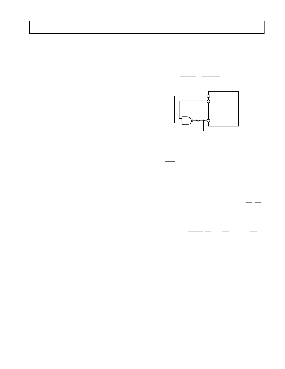
ister. Individual interrupt requests are logically ANDed
with the bits in IMASK; the highest priority unmasked in-
terrupt is then selected. The power-down interrupt is non-
maskable.
ADSP-218xN series members mask all interrupts for one
instruction cycle following the execution of an instruction
that modifies the IMASK register. This does not affect serial
port autobuffering or DMA transfers.
The interrupt control register, ICNTL, controls interrupt
nesting and defines the IRQ0, IRQ1, and IRQ2 external
interrupts to be either edge- or level-sensitive. The IRQE
pin is an external edge-sensitive interrupt and can be forced
and cleared. The IRQL0 and IRQL1 pins are external level
sensitive interrupts.
The IFC register is a write-only register used to force and
clear interrupts. On-chip stacks preserve the processor
status and are automatically maintained during interrupt
handling. The stacks are 12 levels deep to allow interrupt,
loop, and subroutine nesting. The following instructions
allow global enable or disable servicing of the interrupts
(including power-down), regardless of the state of IMASK:
ENA INTS;
DIS INTS;
Disabling the interrupts does not affect serial port auto-
buffering or DMA. When the processor is reset, interrupt
servicing is enabled.
LOW-POWER OPERATION
ADSP-218xN series members have three low-power modes
that significantly reduce the power dissipation when the
device operates under standby conditions. These modes are:
∑ Power-Down
∑ Idle
∑ Slow Idle
The CLKOUT pin may also be disabled to reduce external
power dissipation.
Power-Down
ADSP-218xN series members have a low-power feature that
lets the processor enter a very low-power dormant state
through hardware or software control. Following is a brief
list of power-down features. Refer to the ADSP-218x DSP
Hardware Reference, "System Interface" chapter, for detailed
information about the power-down feature.
∑ Quick recovery from power-down. The processor begins
executing instructions in as few as 200 CLKIN cycles.
∑ Support for an externally generated TTL or CMOS
processor clock. The external clock can continue running
during power-down without affecting the lowest power
rating and 200 CLKIN cycle recovery.
∑ Support for crystal operation includes disabling the oscil-
lator to save power (the processor automatically waits
approximately 4096 CLKIN cycles for the crystal oscilla-
tor to start or stabilize), and letting the oscillator run to
allow 200 CLKIN cycle start-up.
∑ Power-down is initiated by either the power-down pin
(PWD) or the software power-down force bit. Interrupt
support allows an unlimited number of instructions to be
executed before optionally powering down. The power-
down interrupt also can be used as a nonmaskable, edge-
sensitive interrupt.
∑ Context clear/save control allows the processor to
continue where it left off or start with a clean context when
leaving the power-down state.
Table 6. Interrupt Priority and Interrupt Vector
Addresses
Source Of Interrupt
Interrupt Vector Address
(Hex)
Reset (or Power-Up with
PUCR = 1)
0x0000 (Highest Priority)
Power-Down
(Nonmaskable)
0x002C
IRQ2
0x0004
IRQL1
0x0008
IRQL0
0x000C
SPORT0 Transmit
0x0010
SPORT0 Receive
0x0014
IRQE
0x0018
BDMA Interrupt
0x001C
SPORT1 Transmit or
IRQ1
0x0020
SPORT1 Receive or IRQ0
0x0024
Timer
0x0028 (Lowest Priority)
≠9≠
REV. 0
ADSP-218xN Series
∑ The RESET pin also can be used to terminate power-
down.
∑ Power-down acknowledge pin (PWDACK) indicates
when the processor has entered power-down.
Idle
When the ADSP-218xN is in the Idle Mode, the processor
waits indefinitely in a low-power state until an interrupt
occurs. When an unmasked interrupt occurs, it is serviced;
execution then continues with the instruction following the
IDLE instruction. In Idle mode IDMA, BDMA, and auto-
buffer cycle steals still occur.
Slow Idle
The IDLE instruction is enhanced on ADSP-218xN series
members to let the processor's internal clock signal be
slowed, further reducing power consumption. The reduced
clock frequency, a programmable fraction of the normal
clock rate, is specified by a selectable divisor given in the
IDLE instruction.
The format of the instruction is:
IDLE (N);
where
N
= 16, 32, 64, or 128. This instruction keeps the
processor fully functional, but operating at the slower clock
rate. While it is in this state, the processor's other internal
clock signals, such as SCLK, CLKOUT, and timer clock,
are reduced by the same ratio. The default form of the in-
struction, when no clock divisor is given, is the standard
IDLE instruction.
When the IDLE (n) instruction is used, it effectively slows
down the processor's internal clock and thus its response
time to incoming interrupts. The one-cycle response time
of the standard idle state is increased by n, the clock divisor.
When an enabled interrupt is received, ADSP-218xN series
members remain in the idle state for up to a maximum of n
processor cycles (n = 16, 32, 64, or 128) before resuming
normal operation.
When the IDLE (n) instruction is used in systems that have
an externally generated serial clock (SCLK), the serial clock
rate may be faster than the processor's reduced internal
clock rate. Under these conditions, interrupts must not be
generated at a faster rate than can be serviced, due to the
additional time the processor takes to come out of the idle
state (a maximum of n processor cycles).
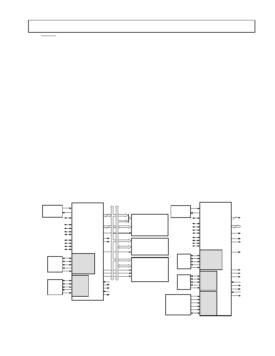
SYSTEM INTERFACE
Figure 1
shows typical basic system configurations with the
ADSP-218xN series, two serial devices, a byte-wide
EPROM, and optional external program and data overlay
memories (mode-selectable). Programmable wait state gen-
eration allows the processor to connect easily to slow periph-
eral devices. ADSP-218xN series members also provide
four external interrupts and two serial ports or six external
interrupts and one serial port. Host Memory Mode allows
access to the full external data bus, but limits addressing to
a single address bit (A0). Through the use of external hard-
ware, additional system peripherals can be added in this
mode to generate and latch address signals.
Figure 1. Basic System Interface
In
ser
t s
yst
em
in
ter
fac
e d
iag
ram
he
re
1/2X CLOCK
OR
CRYSTAL
FL0≠2
CLKIN
XTAL
SERIAL
DEVICE
SCLK1
RFS1 OR
IRQ0
TFS1 OR
IRQ1
DT1 OR FO
DR1 OR FI
SPORT1
SERIAL
DEVICE
A0≠A21
DATA
BYTE
MEMORY
I/O SPACE
(PERIPHERALS)
DATA
ADDR
DATA
ADDR
2048 LOCATIONS
OVERLAY
MEMORY
TWO 8K
PM SEGMENTS
D23≠0
A13≠0
D23≠8
A10≠0
D15≠8
D23≠16
A13≠0
14
24
SCLK0
RFS0
TFS0
DT0
DR0
SPORT0
DATA23≠0
ADSP-218xN
CS
CS
1/2X CLOCK
OR
CRYSTAL
CLKIN
XTAL
FL0≠2
SERIAL
DEVICE
SCLK1
RFS1 OR
IRQ0
TFS1 OR
IRQ1
DT1 OR FO
DR1 OR FI
SPORT1
16
IDMA PORT
IRD
/D6
I
WR
/D7
IS
/D4
IAL/D5
IACK
/D3
IAD15-0
SERIAL
DEVICE
SCLK0
RFS0
TFS0
DT0
DR0
SPORT0
1
16
A0
DATA23≠8
IOMS
BMS
DMS
CMS
BR
BG
BGH
PWD
PWDACK
HOST MEMORY MODE
FULL MEMORY MODE
MODE D/PF3
MODE C/PF2
MODE B/PF1
MODE A/PF0
IRQ2
/PF7
IRQE
/PF4
IRQL0
/PF5
I
RQL1
/PF6
MODE D/PF3
MODE C/PF2
MODE B/PF1
MODE A/PF0
WR
RD
SYSTEM
INTERFACE
OR
ĶCONTROLLER
IRQ2
/PF7
IRQE
/PF4
IRQL0
/PF5
IRQL1
/PF6
IOMS
BMS
PMS
CMS
BR
BG
BGH
PWD
PWDACK
WR
RD
ADSP-218xN
DMS
TWO 8K
DM SEGMENTS
PMS
ADDR13≠0

ADSP-218xN Series
≠10≠
REV. 0
Clock Signals
ADSP-218xN series members can be clocked by either a
crystal or a TTL-compatible clock signal.
The CLKIN input cannot be halted, changed during oper-
ation, nor operated below the specified frequency during
normal operation. The only exception is while the processor
is in the power-down state. For additional information, refer
to the ADSP-218x DSP Hardware Reference, for detailed
information on this power-down feature.
If an external clock is used, it should be a TTL-compatible
signal running at half the instruction rate. The signal is
connected to the processor's CLKIN input. When an exter-
nal clock is used, the XTAL pin must be left unconnected.
ADSP-218xN series members use an input clock with a
frequency equal to half the instruction rate; a 40 MHz input
clock yields a 12.5 ns processor cycle (which is equivalent
to 80 MHz). Normally, instructions are executed in a single
processor cycle. All device timing is relative to the internal
instruction clock rate, which is indicated by the CLKOUT
signal when enabled.
Because ADSP-218xN series members include an on-chip
oscillator circuit, an external crystal may be used. The
crystal should be connected across the CLKIN and XTAL
pins, with two capacitors connected as shown in
Figure 2
.
Capacitor values are dependent on crystal type and should
be specified by the crystal manufacturer. A parallel-
resonant, fundamental frequency, microprocessor-grade
crystal should be used.
A clock output (CLKOUT) signal is generated by the pro-
cessor at the processor's cycle rate. This can be enabled and
disabled by the CLKODIS bit in the SPORT0 Autobuffer
Control Register.
RESET
The RESET signal initiates a master reset of the ADSP-
218xN. The RESET signal must be asserted during the
power-up sequence to assure proper initialization. RESET
during initial power-up must be held long enough to allow
the internal clock to stabilize. If RESET is activated any time
after power-up, the clock continues to run and does not
require stabilization time.
The power-up sequence is defined as the total time required
for the crystal oscillator circuit to stabilize after a valid V
DD
is applied to the processor, and for the internal phase-locked
loop (PLL) to lock onto the specific crystal frequency. A
minimum of 2000 CLKIN cycles ensures that the PLL has
locked, but does not include the crystal oscillator start-up
time. During this power-up sequence the RESET signal
should be held low. On any subsequent resets, the RESET
signal must meet the minimum pulse-width specification
(t
RSP
).
The RESET input contains some hysteresis; however, if an
RC circuit is used to generate the RESET signal, the use of
an external Schmitt trigger is recommended.
The master reset sets all internal stack pointers to the empty
stack condition, masks all interrupts, and clears the MSTAT
register. When RESET is released, if there is no pending
bus request and the chip is configured for booting, the boot-
loading sequence is performed. The first instruction is
fetched from on-chip program memory location 0x0000
once boot loading completes.
POWER SUPPLIES
ADSP-218xN series members have separate power supply
connections for the internal (V
DDINT
) and external (V
DDEXT
)
power supplies. The internal supply must meet the 1.8 V
requirement. The external supply can be connected to a
1.8 V, 2.5 V, or 3.3 V supply. All external supply pins must
be connected to the same supply. All input and I/O pins can
tolerate input voltages up to 3.6 V, regardless of the external
supply voltage. This feature provides maximum flexibility
in mixing 1.8 V, 2.5 V, or 3.3 V components.
Figure 2. External Crystal Connections
CLKIN
CLKOUT
XTAL
DSP
≠11≠
REV. 0
ADSP-218xN Series
MODES OF OPERATION
The ADSP-218xN series modes of operation appear in
Table 7
.
Setting Memory Mode
Memory Mode selection for the ADSP-218xN series is
made during chip reset through the use of the Mode C pin.
This pin is multiplexed with the DSP's PF2 pin, so care must
be taken in how the mode selection is made. The two meth-
ods for selecting the value of Mode C are active and passive.
Passive Configuration
Passive Configuration involves the use of a pull-up or pull-
down resistor connected to the Mode C pin. To minimize
power consumption, or if the PF2 pin is to be used as
an output in the DSP application, a weak pull-up or pull-
down resistance, on the order of 10 k
, can be used. This
value should be sufficient to pull the pin to the desired level
and still allow the pin to operate as a programmable flag
output without undue strain on the processor's output
driver. For minimum power consumption during power-
down, reconfigure PF2 to be an input, as the pull-up or pull-
down resistance will hold the pin in a known state, and will
not switch.
Active Configuration
Active Configuration involves the use of a three-statable
external driver connected to the Mode C pin. A driver's
output enable should be connected to the DSP's RESET
signal such that it only drives the PF2 pin when RESET is
active (low). When RESET is deasserted, the driver should
be three-state, thus allowing full use of the PF2 pin as either
an input or output. To minimize power consumption during
power-down, configure the programmable flag as an output
when connected to a three-stated buffer. This ensures that
the pin will be held at a constant level, and will not oscillate
should the three-state driver's level hover around the logic
switching point.
IDMA ACK Configuration
Mode D = 0 and in host mode: IACK is an active, driven
signal and cannot be "wire ORed." Mode D = 1 and in host
mode: IACK is an open drain and requires an external
pull-down, but multiple IACK pins can be "wire ORed"
together.
Table 7. Modes of Operation
Mode D
Mode C
Mode B
Mode A
Booting Method
X
0
0
0
BDMA feature is used to load the first 32 program memory words
from the byte memory space. Program execution is held off until all
32 words have been loaded. Chip is configured in Full Memory
Mode.
1
X
0
1
0
No automatic boot operations occur. Program execution starts at
external memory location 0. Chip is configured in Full Memory
Mode. BDMA can still be used, but the processor does not automat-
ically use or wait for these operations.
0
1
0
0
BDMA feature is used to load the first 32 program memory words
from the byte memory space. Program execution is held off until all
32 words have been loaded. Chip is configured in Host Mode. IACK
has active pull-down. (Requires additonal hardware.)
0
1
0
1
IDMA feature is used to load any internal memory as desired.
Program execution is held off until the host writes to internal
program memory location 0. Chip is configured in Host Mode.
IACK has active pull-down.
1
1
1
0
0
BDMA feature is used to load the first 32 program memory words
from the byte memory space. Program execution is held off until all
32 words have been loaded. Chip is configured in Host Mode; IACK
requires external pull-down. (Requires additonal hardware.)
1
1
0
1
IDMA feature is used to load any internal memory as desired.
Program execution is held off until the host writes to internal
program memory location 0. Chip is configured in Host Mode.
IACK requires external pull-down.
1
1
Considered as standard operating settings. Using these configurations allows for easier design and better memory management.
ADSP-218xN Series
≠12≠
REV. 0
MEMORY ARCHITECTURE
The ADSP-218xN series provides a variety of memory and
peripheral interface options. The key functional groups are
Program Memory, Data Memory, Byte Memory, and I/O.
Refer to
Figure 3
through
Figure 8
,
Table 8 on page 14
, and
Table 9 on page 14
for PM and DM memory allocations in
the ADSP-218xN series.
Figure 3. ADSP-2184 Memory Architecture
Figure 4. ADSP-2185 Memory Architecture
Figure 5. ADSP-2186 Memory Architecture
PROGRAM MEMORY
PM OVERLAY 1,2
(EXTERNAL PM)
INTERNAL PM
PM OVERLAY 0
(RESERVED)
RESERVED
MODEB = 0
0X3FFF
0X2000
0X0000
0X0FFF
0X1000
0X1FFF
0X3FFF
0X2000
0X0000
0X3FE0
0X3FDF
0X3000
0X2FFF
0X1FFF
DATA MEMORY
DM OVERLAY 1,2
(EXTERNAL DM)
INTERNAL DM
32 MEMORY-MAPPED
CONTROL REGISTERS
4064 RESERVED
WORDS
DM OVERLAY 0
(RESERVED)
PROGRAM MEMORY
RESERVED
EXTERNAL PM
MODEB = 1
0X3FFF
0X2000
0X0000
0X1FFF
PROGRAM MEMORY
PM OVERLAY 1,2
(EXTERNAL PM)
INTERNAL PM
PM OVERLAY 0
(RESERVED)
MODEB = 0
0X3FFF
0X2000
0X0000
0X1FFF
0X3FFF
0X2000
0X0000
0X3FE0
0X3FDF
0X1FFF
DATA MEMORY
DM OVERLAY 1,2
(EXTERNAL DM)
INTERNAL DM
32 MEMORY-MAPPED
CONTROL REGISTERS
DM OVERLAY 0
(INTERNAL DM)
PROGRAM MEMORY
RESERVED
EXTERNAL PM
MODEB = 1
0X3FFF
0X2000
0X0000
0X1FFF
PROGRAM MEMORY
PM OVERLAY 1,2
(EXTERNAL PM)
INTERNAL PM
PM OVERLAY 0
(RESERVED)
MODEB = 0
0X3FFF
0X2000
0X0000
0X1FFF
0X3FFF
0X2000
0X0000
0X3FE0
0X3FDF
0X1FFF
DATA MEMORY
DM OVERLAY 1,2
(EXTERNAL DM)
INTERNAL DM
32 MEMORY-MAPPED
CONTROL REGISTERS
DM OVERLAY 0
(RESERVED)
PROGRAM MEMORY
RESERVED
EXTERNAL PM
MODEB = 1
0X3FFF
0X2000
0X0000
0X1FFF
≠13≠
REV. 0
ADSP-218xN Series
Figure 6. ADSP-2187 Memory Architecture
Figure 7. ADSP-2188 Memory Architecture
Figure 8. ADSP-2189 Memory Architecture
PROGRAM MEMORY
PM OVERLAY 1,2
(EXTERNAL PM)
INTERNAL PM
PM OVERLAY 0,4,5
(INTERNAL PM)
MODEB = 0
0X3FFF
0X2000
0X0000
0X1FFF
0X3FFF
0X2000
0X0000
0X3FE0
0X3FDF
0X1FFF
DATA MEMORY
DM OVERLAY 1,2
(EXTERNAL DM)
INTERNAL DM
32 MEMORY-MAPPED
CONTROL REGISTERS
DM OVERLAY 0,4,5
(INTERNAL DM)
PROGRAM MEMORY
RESERVED
EXTERNAL PM
MODEB = 1
0X3FFF
0X2000
0X0000
0X1FFF
PROGRAM MEMORY
PM OVERLAY 1,2
(EXTERNAL PM)
INTERNAL PM
PM OVERLAY
0,4,5,6,7
(INTERNAL PM)
MODEB = 0
0x3FFF
0x2000
0x0000
0x1FFF
0x3FFF
0x2000
0x0000
0x3FE0
0x3FDF
0x1FFF
DATA MEMORY
DM OVERLAY 1,2
(EXTERNAL DM)
INTERNAL DM
32 MEMORY-MAPPED
CONTROL REGISTERS
DM OVERLAY
0,4,5,6,7,8
(INTERNAL DM)
PROGRAM MEMORY
RESERVED
EXTERNAL PM
MODEB = 1
0x3FFF
0x2000
0x0000
0x1FFF
PROGRAM MEMORY
PM OVERLAY 1,2
(EXTERNAL PM)
INTERNAL PM
PM OVERLAY 0,4,5
(INTERNAL PM)
MODEB = 0
0X3FFF
0X2000
0X0000
0X1FFF
0X3FFF
0X2000
0X0000
0X3FE0
0X3FDF
0X1FFF
DATA MEMORY
DM OVERLAY 1,2
(EXTERNAL DM)
INTERNAL DM
32 MEMORY-MAPPED
CONTROL REGISTERS
DM OVERLAY
0,4,5,6,7
(INTERNAL DM)
PROGRAM MEMORY
RESERVED
EXTERNAL PM
MODEB = 1
0X3FFF
0X2000
0X0000
0X1FFF

ADSP-218xN Series
≠14≠
REV. 0
Program Memory
Program Memory (Full Memory Mode) is a 24-bit-wide
space for storing both instruction opcodes and data. The
ADSP-218xN series has up to 48K words of Program
Memory RAM on chip, and the capability of accessing up
to two 8K external memory overlay spaces, using the exter-
nal data bus.
Program Memory (Host Mode) allows access to all internal
memory. External overlay access is limited by a single exter-
nal address line (A0). External program execution is not
available in host mode due to a restricted data bus that is
only 16 bits wide.
Data Memory
Data Memory (Full Memory Mode) is a 16-bit-wide space
used for the storage of data variables and for memory-
mapped control registers. The ADSP-218xN series has up
to 56K words of Data Memory RAM on-chip. Part of this
space is used by 32 memory-mapped registers. Support also
exists for up to two 8K external memory overlay spaces
through the external data bus. All internal accesses com-
plete in one cycle. Accesses to external memory are timed
using the wait states specified by the DWAIT register and
the wait state mode bit.
Data Memory (Host Mode) allows access to all internal
memory. External overlay access is limited by a single exter-
nal address line (A0).
Table 8. PMOVLAY Bits
Processor
PMOVLAY
Memory
A13
A12 ≠0
ADSP-2184N
No Internal
Overlay Region
Not Applicable
Not Applicable
Not Applicable
ADSP-2185N
0
Internal Overlay
Not Applicable
Not Applicable
ADSP-2186N
No Internal
Overlay Region
Not Applicable
Not Applicable
Not Applicable
ADSP-2187N
0, 4, 5
Internal Overlay
Not Applicable
Not Applicable
ADSP-2188N
0, 4, 5, 6, 7
Internal Overlay
Not Applicable
Not Applicable
ADSP-2189N
0, 4, 5
Internal Overlay
Not Applicable
Not Applicable
All Processors
1
External Overlay 1
0
13 LSBs of Address Between 0x2000 and
0x3FFF
All Processors
2
External Overlay 2
1
13 LSBs of Address Between 0x2000 and
0x3FFF
Table 9. DMOVLAY Bits
Processor
DMOVLAY
Memory
A13
A12≠0
ADSP-2184N
No Internal Overlay
Region
Not Applicable
Not Applicable
Not Applicable
ADSP-2185N
0
Internal Overlay
Not Applicable
Not Applicable
ADSP-2186N
No Internal Overlay
Region
Not Applicable
Not Applicable
Not Applicable
ADSP-2187N
0, 4, 5
Internal Overlay
Not Applicable
Not Applicable
ADSP-2188N
0, 4, 5, 6, 7, 8
Internal Overlay
Not Applicable
Not Applicable
ADSP-2189N
0, 4, 5, 6, 7
Internal Overlay
Not Applicable
Not Applicable
All Processors
1
External Overlay 1
0
13 LSBs of Address
Between 0x0000
and 0x1FFF
All Processors
2
External Overlay 2
1
13 LSBs of Address
Between 0x0000
and 0x1FFF
≠15≠
REV. 0
ADSP-218xN Series
Memory-Mapped Registers (New to the ADSP-218xM
and N series)
ADSP-218xN series members have three memory-mapped
registers that differ from other ADSP-21xx Family DSPs.
The slight modifications to these registers (Wait State Con-
trol, Programmable Flag and Composite Select Control,
and System Control) provide the ADSP-218xN's wait state
and BMS control features. Default bit values at reset are
shown; if no value is shown, the bit is undefined at reset.
Reserved bits are shown on a grey field. These bits should
always be written with zeros.
I/O Space (Full Memory Mode)
ADSP-218xN series members support an additional exter-
nal memory space called I/O space. This space is designed
to support simple connections to peripherals (such as data
converters and external registers) or to bus interface ASIC
data registers. I/O space supports 2048 locations of 16-bit
wide data. The lower eleven bits of the external address bus
are used; the upper three bits are undefined.
Two instructions were added to the core ADSP-2100
Family instruction set to read from and write to I/O memory
space. The I/O space also has four dedicated three-bit wait
state registers, IOWAIT0 ≠ 3 as shown in
Figure 9
, which in
combination with the wait state mode bit, specify up to 15
wait states to be automatically generated for each of four
regions. The wait states act on address ranges, as shown
in
Table 10
.
Note: In Full Memory Mode, all 2048 locations of I/O space
are directly addressable. In Host Memory Mode, only
address pin A0 is available; therefore, additional logic is
required externally to achieve complete addressability of the
2048 I/O space locations.
Composite Memory Select
ADSP-218xN series members have a programmable
memory select signal that is useful for generating memory
select signals for memories mapped to more than one space.
The CMS signal is generated to have the same timing as
each of the individual memory select signals (PMS, DMS,
BMS, IOMS) but can combine their functionality. Each bit
in the CMSSEL register, when set, causes the CMS signal
to be asserted when the selected memory select is asserted.
For example, to use a 32K word memory to act as both
program and data memory, set the PMS and DMS bits in
the CMSSEL register and use the CMS pin to drive the chip
select of the memory, and use either DMS or PMS as the
additional address bit.
The CMS pin functions like the other memory select signals
with the same timing and bus request logic. A 1 in the enable
bit causes the assertion of the CMS signal at the same time
as the selected memory select signal. All enable bits default
to 1 at reset, except the BMS bit.
See
Figure 10
and
Figure 11
for illustration of the program-
mable flag and composite control register and the system
control register.
Table 10. Wait States
Address Range
Wait State Register
0x000≠0x1FF
IOWAIT0 and Wait State Mode
Select Bit
0x200≠0x3FF
IOWAIT1 and Wait State Mode
Select Bit
0x400≠0x5FF
IOWAIT2 and Wait State Mode
Select Bit
0x600≠0x7FF
IOWAIT3 and Wait State Mode
Select Bit
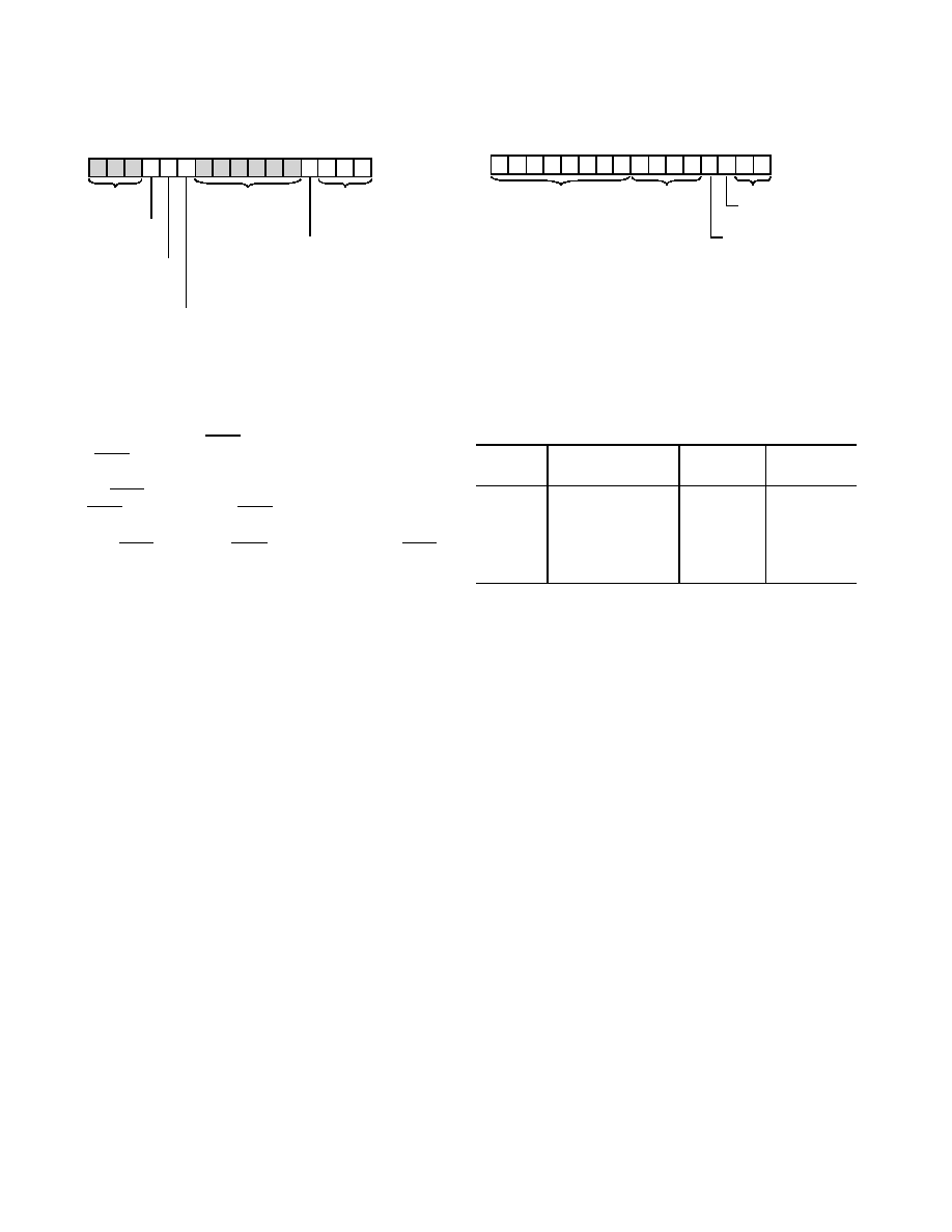
Figure 9. Wait State Control Register
Figure 10. Programmable Flag and Composite Control
Register
In
ser
t W
ait
St
ate
C
on
tro
l R
eg
ist
er
DWAIT
IOWAIT3
IOWAIT2
IOWAIT1
IOWAIT0
DM(0X3FFE)
WAIT STATE CONTROL
1
1
1
1
1
1
1
1
1
1
1
1
1
1
1
1
15 14
13 12 11 10
9
8
7
6
5
4
3
2
1
0
WAIT STATE MODE SELECT
0 = NORMAL MODE (PWAIT, DWAIT, IOWAIT0≠3 = N WAIT STATES,
RANGING FROM 0 TO 7)
1 = 2N + 1 MODE (PWAIT, DWAIT, IOWAIT0≠3 = 2N + 1 WAIT STATES,
RANGING FROM 0 TO 15)
B M W A I T
C M S S E L
0 = D IS A B L E
CMS
1 = E N A B L E
CMS
DM(0X3FE6)
P F T Y P E
0 = I N P U T
1 = O U T P U T
( W H E R E B IT : 1 1 - I O M , 1 0 - B M , 9 - D M , 8 - P M )
1
1
1
1
1
0
1
1
0
0
0
0
0
0
0
0
15 14
13 12
11 10
9
8
7
6
5
4
3
2
1
0
PROGRAMMABLE FLAG AND COMPOSITE
SELECT CONTROL
ADSP-218xN Series
≠16≠
REV. 0
Byte Memory Select
The ADSP-218xN's BMS disable feature combined with
the CMS pin allows use of multiple memories in the byte
memory space. For example, an EPROM could be attached
to the BMS select, and a flash memory could be connected
to CMS. Because at reset BMS is enabled, the EPROM
would be used for booting. After booting, software could
disable BMS and set the CMS signal to respond to BMS,
enabling the flash memory.
Byte Memory
The byte memory space is a bidirectional, 8-bit-wide,
external memory space used to store programs and data.
Byte memory is accessed using the BDMA feature. The byte
memory space consists of 256 pages, each of which is
16K
8 bits.
The byte memory space on the ADSP-218xN series sup-
ports read and write operations as well as four different data
formats. The byte memory uses data bits 15 ≠8 for data. The
byte memory uses data bits 23 ≠ 16 and address bits 13 ≠ 0
to create a 22-bit address. This allows up to a 4 meg
8
(32 megabit) ROM or RAM to be used without glue logic.
All byte memory accesses are timed by the BMWAIT reg-
ister and the wait state mode bit.
Byte Memory DMA (BDMA, Full Memory Mode)
The byte memory DMA controller (
Figure 12
) allows
loading and storing of program instructions and data using
the byte memory space. The BDMA circuit is able to access
the byte memory space while the processor is operating
normally and steals only one DSP cycle per 8-, 16-, or 24-
bit word transferred.
The BDMA circuit supports four different data formats that
are selected by the BTYPE register field. The appropriate
number of 8-bit accesses are done from the byte memory
space to build the word size selected.
Table 11
shows the
data formats supported by the BDMA circuit.
Unused bits in the 8-bit data memory formats are filled with
0s. The BIAD register field is used to specify the starting
address for the on-chip memory involved with the transfer.
The 14-bit BEAD register specifies the starting address for
the external byte memory space. The 8-bit BMPAGE reg-
ister specifies the starting page for the external byte memory
space. The BDIR register field selects the direction of the
transfer. Finally, the 14-bit BWCOUNT register specifies
the number of DSP words to transfer and initiates the
BDMA circuit transfers.
BDMA accesses can cross page boundaries during sequen-
tial addressing. A BDMA interrupt is generated on the com-
pletion of the number of transfers specified by the
BWCOUNT register.
The BWCOUNT register is updated after each transfer so
it can be used to check the status of the transfers. When
it reaches zero, the transfers have finished and a BDMA
interrupt is generated. The BMPAGE and BEAD registers
must not be accessed by the DSP during BDMA operations.
The source or destination of a BDMA transfer will always
be on-chip program or data memory.
When the BWCOUNT register is written with a nonzero
value the BDMA circuit starts executing byte memory
accesses with wait states set by BMWAIT. These accesses
continue until the count reaches zero. When enough access-
es have occurred to create a destination word, it is trans-
ferred to or from on-chip memory. The transfer takes one
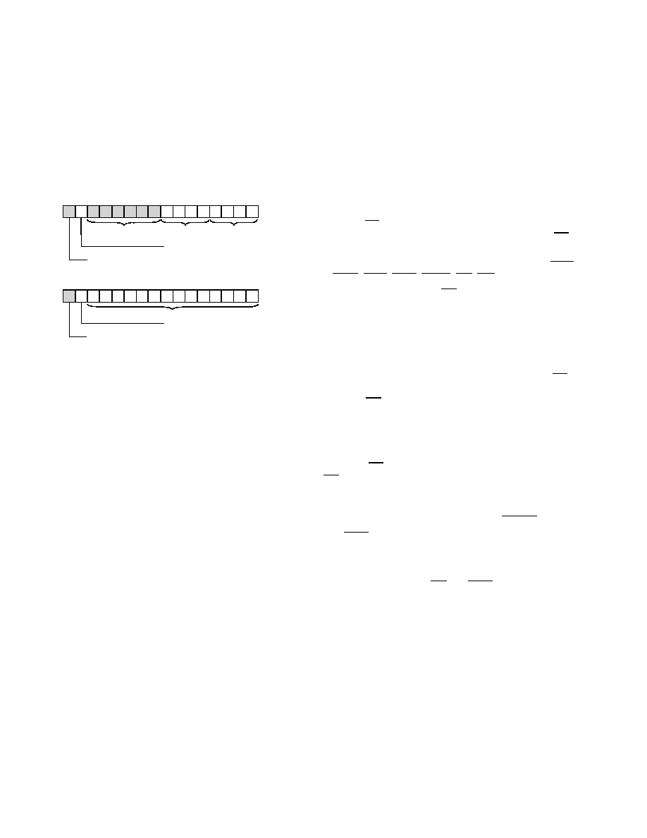
Figure 11. System Control Register
RESERV ED, A L WAYS
SET T O 0
SPORT 0 ENABL E
0 = DISABL E
1 = ENABL E
DM(0X3FF F)
SYSTEM CONTROL
SPORT 1 ENABLE
0 = DISABL E
1 = ENABLE
SPORT1 CONFIGURE
0 = FI, FO,
IRQ0
,
IRQ1
, SC L K
1 = SPORT1
DI SA BL E
BMS
0 = EN AB LE
BMS
1 = DISA B L E
BMS
PWAIT
PROGRAM MEM ORY
WAIT ST ATES
0
0
0
0
0
1
0
0
0
0
0
0
0
1
1
1
15 14 13 12 11 10
9
8
7
6
5
4
3
2
1
0
NOT E: RESERVED B IT S ARE SHOWN O N A GRAY FIEL D. THESE B IT S
SHOULD ALWAYS BE WRITT EN WITH Z EROS.
RESE RVED
SET T O 0
Figure 12. BDMA Control Register
Table 11. Data Formats
BTYPE
Internal
Memory Space
Word Size
Alignment
00
Program
Memory
24
Full Word
01
Data Memory
16
Full Word
10
Data Memory
8
MSBs
11
Data Memory
8
LSBs
BDMA CONTROL
BMPAGE
BTYPE
BDIR
0 = LOAD FROM BM
1 = STORE TO BM
BCR
0 = RUN DURING BDMA
1 = HALT DURING BDMA
0
0
0
0
0
0
0
0
0
0
0
0
1
0
0
0
15 14 13 12 11 10
9
8
7
6
5
4
3
2
1
0
DM (0x3FE3)
BDMA
OVERLAY
BITS
(SEE TABLE 12)

≠17≠
REV. 0
ADSP-218xN Series
DSP cycle. DSP accesses to external memory have priority
over BDMA byte memory accesses.
The BDMA Context Reset bit (BCR) controls whether the
processor is held off while the BDMA accesses are occur-
ring. Setting the BCR bit to 0 allows the processor to con-
tinue operations. Setting the BCR bit to 1 causes the
processor to stop execution while the BDMA accesses are
occurring, to clear the context of the processor, and start
execution at address 0 when the BDMA accesses have
completed.
The BDMA overlay bits specify the OVLAY memory blocks
to be accessed for internal memory. Set these bits as indi-
cated in.
Note: BDMA cannot access external overlay memory
regions 1 and 2.
The BMWAIT field, which has four bits on ADSP-218xN
series members, allows selection up to 15 wait states for
BDMA transfers.
Internal Memory DMA Port (IDMA Port; Host Memory
Mode)
The IDMA Port provides an efficient means of communi-
cation between a host system and ADSP-218xN series
members. The port is used to access the on-chip program
memory and data memory of the DSP with only one DSP
cycle per word overhead. The IDMA port cannot, however,
be used to write to the DSP's memory-mapped control reg-
isters. A typical IDMA transfer process is shown as follows:
1.
Host starts IDMA transfer.
2.
Host checks IACK control line to see if the DSP is
busy.
3.
Host uses IS and IAL control lines to latch either the
DMA starting address (IDMAA) or the PM/DM
OVLAY selection into the DSP's IDMA control regis-
ters. If Bit 15 = 1, the value of bits 7≠0 represent the
IDMA overlay; bits 14≠8 must be set to 0. If Bit 15 = 0,
the value of Bits 13≠0 represent the starting address
of internal memory to be accessed and Bit 14 reflects
PM or DM for access. Set IDDMOVLAY and
IDPMOVLAY bits in the IDMA overlay register as
indicted in
Table 12
.
4.
Host uses IS and IRD (or IWR) to read (or write) DSP
internal memory (PM or DM).
5.
Host checks IACK line to see if the DSP has completed
the previous IDMA operation.
6.
Host ends IDMA transfer.
The IDMA port has a 16-bit multiplexed address and data
bus and supports 24-bit program memory. The IDMA port
is completely asynchronous and can be written while the
ADSP-218xN is operating at full speed.
The DSP memory address is latched and then automatically
incremented after each IDMA transaction. An external
device can therefore access a block of sequentially addressed
memory by specifying only the starting address of the block.
This increases throughput as the address does not have to
be sent for each memory access.
IDMA Port access occurs in two phases. The first is the
IDMA Address Latch cycle. When the acknowledge is as-
serted, a 14-bit address and 1-bit destination type can be
driven onto the bus by an external device. The address spec-
ifies an on-chip memory location, the destination type spec-
ifies whether it is a DM or PM access. The falling edge of
the IDMA address latch signal (IAL) or the missing edge of
the IDMA select signal (IS) latches this value into the
IDMAA register.
Once the address is stored, data can be read from, or written
to, the ADSP-218xN's on-chip memory. Asserting the
select line (IS) and the appropriate read or write line (IRD
and IWR respectively) signals the ADSP-218xN that a par-
ticular transaction is required. In either case, there is a one-
processor-cycle delay for synchronization. The memory
access consumes one additional processor cycle.
Once an access has occurred, the latched address is auto-
matically incremented, and another access can occur.
Through the IDMAA register, the DSP can also specify the
starting address and data format for DMA operation.
Asserting the IDMA port select (IS) and address latch
enable (IAL) directs the ADSP-218xN to write the address
onto the IAD14 ≠ 0 bus into the IDMA Control Register
(
Figure 13
). If Bit 15 is set to 0, IDMA latches the address.
If Bit 15 is set to 1, IDMA latches into the OVLAY register.
This register, also shown in
Figure 13
, is memory-mapped
at address DM (0x3FE0). Note that the latched address
(IDMAA) cannot be read back by the host.
When Bit 14 in 0x3FE7 is set to zero, short reads use the
timing shown in
Figure 34 on page 37
. When Bit 14 in
0x3FE7 is set to 1, timing in
Figure 35 on page 38
applies
for short reads in short read only mode. Set IDDMOVLAY
Table 12. IDMA/BDMA Overlay Bits
Processor
IDMA/BDMA
PMOVLAY
IDMA/BDMA
DMOVLAY
ADSP-2184N
ADSP-2185N
ADSP-2186N
ADSP-2187N
ADSP-2188N
0
0
0
0, 4, 5
0, 4, 5, 6, 7
0
0
0
0, 4, 5
0, 4, 5, 6, 7, 8
ADSP-2189N
0, 4, 5
0, 4, 5, 6, 7
ADSP-218xN Series
≠18≠
REV. 0
and IDPMOVLAY bits in the IDMA overlay register as
indicated in
Table 12
. Refer to the ADSP-218x DSP Hard-
ware Reference for additional details.
Note: In full memory mode all locations of 4M-byte
memory space are directly addressable. In host memory
mode, only address pin A0 is available, requiring additional
external logic to provide address information for the byte.
Bootstrap Loading (Booting)
ADSP-218xN series members have two mechanisms to
allow automatic loading of the internal program memory
after reset. The method for booting is controlled by the
Mode A, B, and C configuration bits.
When the mode pins specify BDMA booting, the ADSP-
218xN initiates a BDMA boot sequence when reset is
released.
The BDMA interface is set up during reset to the following
defaults when BDMA booting is specified: the BDIR,
BMPAGE, BIAD, and BEAD registers are set to 0, the
BTYPE register is set to 0 to specify program memory 24-
bit words, and the BWCOUNT register is set to 32. This
causes 32 words of on-chip program memory to be loaded
from byte memory. These 32 words are used to set up the
BDMA to load in the remaining program code. The BCR
bit is also set to 1, which causes program execution to be
held off until all 32 words are loaded into on-chip program
memory. Execution then begins at address 0.
The ADSP-2100 Family development software (Revision
5.02 and later) fully supports the BDMA booting feature
and can generate byte memory space-compatible boot code.
The IDLE instruction can also be used to allow the proces-
sor to hold off execution while booting continues through
the BDMA interface. For BDMA accesses while in Host
Mode, the addresses to boot memory must be constructed
externally to the ADSP-218xN. The only memory address
bit provided by the processor is A0.
IDMA Port Booting
ADSP-218xN series members can also boot programs
through its Internal DMA port. If Mode C = 1, Mode B =
0, and Mode A = 1, the ADSP-218xN boots from the IDMA
port. IDMA feature can load as much on-chip memory as
desired. Program execution is held off until the host writes
to on-chip program memory location 0.
BUS REQUEST AND BUS GRANT
ADSP-218xN series members can relinquish control of the
data and address buses to an external device. When the
external device requires access to memory, it asserts the Bus
Request (BR) signal. If the ADSP-218xN is not performing
an external memory access, it responds to the active BR
input in the following processor cycle by:
∑ Three-stating the data and address buses and the PMS,
DMS, BMS, CMS, IOMS, RD, WR output drivers,
∑ Asserting the bus grant (BG) signal, and
∑ Halting program execution.
If Go Mode is enabled, the ADSP-218xN will not halt
program execution until it encounters an instruction that
requires an external memory access.
If an ADSP-218xN series member is performing an external
memory access when the external device asserts the BR
signal, it will not three-state the memory interfaces nor
assert the BG signal until the processor cycle after the access
completes. The instruction does not need to be completed
when the bus is granted. If a single instruction requires two
external memory accesses, the bus will be granted between
the two accesses.
When the BR signal is released, the processor releases the
BG signal, re-enables the output drivers, and continues
program execution from the point at which it stopped.
The bus request feature operates at all times, including
when the processor is booting and when RESET is active.
The BGH pin is asserted when an ADSP-218xN series
member requires the external bus for a memory or BDMA
access, but is stopped. The other device can release the bus
by deasserting bus request. Once the bus is released, the
ADSP-218xN deasserts BG and BGH and executes the
external memory access.
FLAG I/O PINS
ADSP-218xN series members have eight general-purpose
programmable input/output flag pins. They are controlled
by two memory-mapped registers. The PFTYPE register
determines the direction, 1 = output and 0 = input. The
PFDATA register is used to read and write the values on the
pins. Data being read from a pin configured as an input is
synchronized to the ADSP-218xN's clock. Bits that are pro-
grammed as outputs will read the value being output. The
PF pins default to input during reset.
Figure 13. IDMA OVLAY/Control Registers
IDMA OVERLAY
DM (0x3FE7)
RESERVED SET TO 0
IDDMOVLAY
IDPMOVLAY
0
0
0
0
0
0
0
0
0
0
0
0
0
0
0
15 14
13 12
11 10
9
8
7
6
5
4
3
2
1
0
SHORT READ ONLY
0 = DISABLE
1 = ENABLE
IDMA CONTROL (U = UNDEFINED AT RESET)
DM (0x3FE0)
IDMAA ADDRESS
U
U
U
U
U
U
U
U
U
U
U
U
U
U
U
15 14
13 12
11 10
9
8
7
6
5
4
3
2
1
0
IDMAD DESTINATION MEMORY
TYPE
0 = PM
1 = DM
NOTE: RESERVED BITS ARE SHOWN ON A GRAY FIELD. THESE
BITS SHOULD ALWAYS BE WRITTEN WITH ZEROS.
0
RESERVED SET TO 0
0
RESERVED SET TO 0
(SEE TABLE 12)
≠19≠
REV. 0
ADSP-218xN Series
In addition to the programmable flags, ADSP-218xN series
members have five fixed-mode flags, FI, FO, FL0, FL1, and
FL2. FL0 ≠ FL2 are dedicated output flags. FI and FO are
available as an alternate configuration of SPORT1.
Note: Pins PF0, PF1, PF2, and PF3 are also used for device
configuration during reset.
INSTRUCTION SET DESCRIPTION
The ADSP-218xN series assembly language instruction set
has an algebraic syntax that was designed for ease of coding
and readability. The assembly language, which takes full
advantage of the processor's unique architecture, offers the
following benefits:
∑ The algebraic syntax eliminates the need to remember
cryptic assembler mnemonics. For example, a typical
arithmetic add instruction, such as AR = AX0 + AY0,
resembles a simple equation.
∑ Every instruction assembles into a single, 24-bit word that
can execute in a single instruction cycle.
∑ The syntax is a superset ADSP-2100 Family assembly
language and is completely source and object code com-
patible with other family members. Programs may need
to be relocated to utilize on-chip memory and conform to
the ADSP-218xN's interrupt vector and reset vector map.
∑ Sixteen condition codes are available. For conditional
jump, call, return, or arithmetic instructions, the
condition can be checked and the operation executed in
the same instruction cycle.
∑ Multifunction instructions allow parallel execution of an
arithmetic instruction, with up to two fetches or one write
to processor memory space, during a single instruc-
tion cycle.
DESIGNING AN EZ-ICE-COMPATIBLE SYSTEM
ADSP-218xN series members have on-chip emulation
support and an ICE-Port, a special set of pins that interface
to the EZ-ICE. These features allow in-circuit emulation
without replacing the target system processor by using only
a 14-pin connection from the target system to the EZ-ICE.
Target systems must have a 14-pin connector to accept the
EZ-ICE's in-circuit probe, a 14-pin plug.
Note: The EZ-ICE uses the same V
DD
voltage as the V
DD
voltage used for V
DDEXT
. Because the input pins of the
ADSP-218xN series members are tolerant to input voltages
up to 3.6 V, regardless of the value of V
DDEXT
, the voltage
setting for the EZ-ICE must not exceed 3.3 V.
Issuing the chip reset command during emulation causes
the DSP to perform a full chip reset, including a reset of its
memory mode. Therefore, it is vital that the mode pins are
set correctly PRIOR to issuing a chip reset command from
the emulator user interface. If a passive method of maintain-
ing mode information is being used (as discussed in
Setting
Memory Mode on page 11
), it does not matter that the
mode information is latched by an emulator reset. However,
if the RESET pin is being used as a method of setting the
value of the mode pins, the effects of an emulator reset must
be taken into consideration.
One method of ensuring that the values located on the mode
pins are those desired is to construct a circuit like the one
shown in
Figure 14
. This circuit forces the value located on
the Mode A pin to logic high, regardless of whether it is
latched via the RESET or ERESET pin.
The ICE-Port interface consists of the following ADSP-
218xN pins: EBR, EINT, EE, EBG, ECLK, ERESET,
ELIN, EMS, and ELOUT.
These ADSP-218xN pins must be connected only to the
EZ-ICE connector in the target system. These pins have no
function except during emulation, and do not require pull-
up or pull-down resistors. The traces for these signals
between the ADSP-218xN and the connector must be kept
as short as possible, no longer than 3 inches.
The following pins are also used by the EZ-ICE: BR, BG,
RESET, and GND.
The EZ-ICE uses the EE (emulator enable) signal to take
control of the ADSP-218xN in the target system. This
causes the processor to use its ERESET, EBR, and EBG
pins instead of the RESET, BR, and BG pins. The BG
output is three-stated. These signals do not need to be
jumper-isolated in the system.
The EZ-ICE connects to the target system via a ribbon cable
and a 14-pin female plug. The female plug is plugged onto
the 14-pin connector (a pin strip header) on the target
board.
Target Board Connector for EZ-ICE Probe
The EZ-ICE connector (a standard pin strip header) is
shown in
Figure 15
. This connector must be added to the
target board design to use the EZ-ICE. Be sure to allow
enough room in the system to fit the EZ-ICE probe onto
the 14-pin connector.
The 14-pin, 2-row pin strip header is keyed at the Pin 7
location--Pin 7 must be removed from the header. The pins
must be 0.025 inch square and at least 0.20 inch in length.
Figure 14. Mode A Pin/EZ-ICE Circuit
PROGRAMMABLE I/O
MODE A/PF0
RESET
ERESET
ADSP-218xN
1k
ADSP-218xN Series
≠20≠
REV. 0
Pin spacing should be 0.1
0.1 inches. The pin strip header
must have at least 0.15 inch clearance on all sides to accept
the EZ-ICE probe plug.
Pin strip headers are available from vendors such as 3M,
McKenzie, and Samtec.
Target Memory Interface
For the target system to be compatible with the EZ-ICE
emulator, it must comply with the memory interface guide-
lines listed below.
PM, DM, BM, IOM, and CM
Design the Program Memory (PM), Data Memory (DM),
Byte Memory (BM), I/O Memory (IOM), and Composite
Memory (CM) external interfaces to comply with worst-
case device timing requirements and switching characteris-
tics as specified in this data sheet. The performance of the
EZ-ICE may approach published worst-case specification
for some memory access timing requirements and switching
characteristics.
Note: If the target does not meet the worst-case chip spec-
ification for memory access parameters, the circuitry may
not be able to be emulated at the desired CLKIN frequency.
Depending on the severity of the specification violation, the
system may be difficult to manufacture, as DSP compo-
nents statistically vary in switching characteristic and timing
requirements, within published limits.
Restriction: All memory strobe signals on the ADSP-
218xN (RD, WR, PMS, DMS, BMS, CMS, and IOMS)
used in the target system must have 10 k
pull-up resistors
connected when the EZ-ICE is being used. The pull-up
resistors are necessary because there are no internal pull-
ups to guarantee their state during prolonged three-state
conditions resulting from typical EZ-ICE debugging ses-
sions. These resistors may be removed when the EZ-ICE is
not being used.
Target System Interface Signals
When the EZ-ICE board is installed, the performance on
some system signals changes. Design the system to be com-
patible with the following system interface signal changes
introduced by the EZ-ICE board:
∑ EZ-ICE emulation introduces an 8 ns propagation
delay between the target circuitry and the DSP on the
RESET signal.
∑ EZ-ICE emulation introduces an 8 ns propagation
delay between the target circuitry and the DSP on the BR
signal.
∑ EZ-ICE emulation ignores RESET and BR, when
single-stepping.
∑ EZ-ICE emulation ignores RESET and BR when in
Emulator Space (DSP halted).
∑ EZ-ICE emulation ignores the state of target BR in certain
modes. As a result, the target system may take control of
the DSP's external memory bus only if bus grant (BG) is
asserted by the EZ-ICE board's DSP.
Figure 15. Target Board Connector for EZ-ICE
1
2
3
4
5
6
7
8
9
10
11
12
13
14
GND
KEY (NO PIN)
RESET
BR
BG
TOP VIEW
EBG
EBR
ELOUT
EE
EINT
ELIN
ECLK
EMS
ERESET
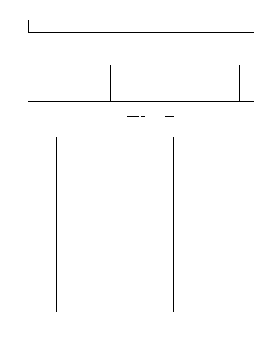
≠21≠
REV. 0
ADSP-218xN Series
SPECIFICATIONS
RECOMMENDED OPERATING CONDITIONS
Parameter
1
K Grade (Commercial)
B Grade (Industrial)
Unit
Min
Max
Min
Max
V
DDINT
1.71
1.89
1.8
2.0
V
V
DDEXT
1.71
3.6
1.8
3.6
V
V
INPUT
2
V
IL
= ≠ 0.3
V
IH
= + 3.6
V
IL
= ≠ 0.3
V
IH
= + 3.6
V
T
AMB
0
70
≠ 40
+ 85
į
C
1
Specifications subject to change without notice.
2
The ADSP-218xN is 3.3 V tolerant (always accepts up to 3.6 V max V
IH
), but voltage compliance (on outputs, V
OH
) depends on the input V
DDEXT
,
because V
OH
(max) approximately equals V
DDEXT
(max). This 3.3 V tolerance applies to bidirectional pins (D23 ≠D 0, RFS0, RFS1, SCLK0, SCLK1,
TFS0, TFS1, A13 ≠A 1, PF7 ≠ PF0) and input-only pins (CLKIN, RESET, BR, DR0, DR1, PWD).
ELECTRICAL CHARACTERISTICS
Parameter
1
Description
Test Conditions
Min
Typ
Max
Unit
V
IH
Hi-Level Input Voltage
2,
3
@ V
DDEXT
= 1.71 to 2.0 V,
V
DDINT
= max
@ V
DDEXT
= 2.1 to 3.6 V,
V
DDINT
= max
1.25
V
V
IL
Lo-Level Input Voltage
2,
3
@ V
DDEXT
2.0 V,
V
DDINT
= min
@ V
DDEXT
2.0 V,
V
DDINT
= min
0.6
0.7
V
V
V
OH
Hi-Level Output Voltage
2,
4,
5
@ V
DDEXT
= 1.71 to 2.0 V,
I
OH
= ≠ 0.5 mA
@ V
DDEXT
= 2.1 to 2.9 V, I
OH
= ≠ 0.5 mA
@ V
DDEXT
= 3.0 to 3.6 V, I
OH
= ≠ 0.5 mA
@ V
DDEXT
= 1.71 to 3.6 V,
I
OH
= ≠ 100
Ķ
A
6
1.35
2.0
2.4
V
DDEXT
≠ 0.3
V
V
V
V
V
OL
Lo-Level Output Voltage
2,
4,
5
@ V
DDEXT
= 1.71 to 3.6 V,
I
OL
= 2.0 mA
0.4
V
I
IH
Hi-Level Input Current
3
@ V
DDINT
= max,
V
IN
= 3.6 V
10
Ķ
A
I
IL
Lo-Level Input Current
3
@ V
DDINT
= max,
V
IN
= 0 V
10
Ķ
A
I
OZH
Three-State Leakage
Current
7
@ V
DDEXT
= max,
V
IN
= 3.6 V
8
10
Ķ
A
I
OZL
Three-State Leakage
Current
7
@ V
DDEXT
= max,
V
IN
= 0 V
8
10
Ķ
A
I
DD
Supply Current (Idle)
9
@ V
DDINT
= 1.8 V,
t
CK
= 12.5 ns,
T
AMB
= 25
į
C
6
mA
I
DD
Supply Current (Dynamic)
10
@ V
DDINT
= 1.8 V,
t
CK
= 12.5 ns
11
,
T
AMB
= 25
į
C
25
mA

ADSP-218xN Series
≠22≠
REV. 0
ABSOLUTE MAXIMUM RATINGS
I
DD
Supply Current (Idle)
9
@ V
DDINT
= 1.9 V,
t
CK
= 12.5 ns,
T
AMB
= 25
į
C
6.5
mA
I
DD
Supply Current (Dynamic)
10
@ V
DDINT
= 1.9 V,
t
CK
= 12.5 ns
11
,
T
AMB
= 25
į
C
26
mA
I
DD
Supply Current (Power-
Down)
12
@ V
DDINT
= 1.8 V,
T
AMB
= 25
į
C
in Lowest Power Mode
100
Ķ
A
C
I
Input Pin Capacitance
3,
6
@ V
IN
= 1.8 V,
f
IN
= 1.0 MHz,
T
AMB
= 25
į
C
8
pF
C
O
Output Pin
Capacitance
6, 7, 12,
13
@ V
IN
= 1.8 V,
f
IN
= 1.0 MHz,
T
AMB
= 25
į
C
8
pF
1
Specifications subject to change without notice.
2
Bidirectional pins: D23 ≠ 0, RFS0, RFS1, SCLK0, SCLK1, TFS0, TFS1, A13 ≠ 1, PF7 ≠0.
3
Input only pins: CLKIN, RESET, BR, DR0, DR1, PWD.
4
Output pins: BG, PMS, DMS, BMS, IOMS, CMS, RD, WR, PWDACK, A0, DT0, DT1, CLKOUT, FL2 ≠ FL0, BGH.
5
Although specified for TTL outputs, all ADSP-218xN outputs are CMOS-compatible and will drive to V
DDEXT
and GND, assuming no dc loads.
6
Guaranteed but not tested.
7
Three-statable pins: A13 ≠ A1, D23 ≠D 0, PMS, DMS, BMS, IOMS, CMS, RD, WR, DT0, DT1, SCLK0, SCLK1, TFS0, TFS1, RFS0, RFS1, PF7 ≠ PF0.
8
0 V on BR.
9
Idle refers to ADSP-218xN state of operation during execution of IDLE instruction. Deasserted pins are driven to either V
DD
or GND.
10
I
DD
measurement taken with all instructions executing from internal memory. 50% of the instructions are multifunction (Types 1, 4, 5, 12, 13, 14), 30%
are Type 2 and Type 6, and 20% are idle instructions.
11
V
IN
= 0 V and 3 V. For typical values for supply currents, refer to Power Dissipation section.
12
See ADSP-218x DSP Hardware Reference for details.
13
Output pin capacitance is the capacitive load for any three-stated output pin.
ELECTRICAL CHARACTERISTICS
(CONTINUED)
Parameter
1
Description
Test Conditions
Min
Typ
Max
Unit
Internal Supply Voltage (V
DDINT
)
1
. . . . . . . . ≠ 0.3 V to + 2.2 V
External Supply Voltage (V
DDEXT
) . . . . . . . . ≠ 0.3 V to + 4.0 V
Input Voltage
2
. . . . . . . . . . . . . . . . . . . . . . ≠ 0.5 V to + 4.0 V
Output Voltage Swing
3
. . . . . . . . . . .≠ 0.5 V to V
DDEXT
+ 0.5 V
Operating Temperature Range . . . . . . . . . . . ≠ 40ļC to + 85ļC
Storage Temperature Range . . . . . . . . . . . . ≠ 65ļC to + 150ļC
Lead Temperature (5 sec) LQFP . . . . . . . . . . . . . . . ≠ 280ļC
1
Stresses greater than those listed above may cause permanent damage to the
device. These are stress ratings only. Functional operation of the device at these
or any other conditions greater than those indicated in the operational sections
of this specification is not implied. Exposure to absolute maximum rating condi-
tions for extended periods may affect device reliability.
2
Applies to Bidirectional pins (D23 ≠ 0, RFS0, RFS1, SCLK0, SCLK1, TFS0,
TFS1, A13 ≠ 1, PF7 ≠ 0) and Input only pins (CLKIN, RESET, BR, DR0, DR1,
PWD).
3
Applies to Output pins (BG, PMS, DMS, BMS, IOMS, CMS, RD, WR,
PWDACK, A0, DT0, DT1, CLKOUT, FL2 ≠ 0, BGH).
≠23≠
REV. 0
ADSP-218xN Series
ESD SENSITIVITY
Power Dissipation
To determine total power dissipation in a specific applica-
tion, the following equation should be applied for each
output: C V
DD
2
f
where: C = load capacitance, f = output switching frequency.
Example: In an application where external data memory
is used and no other outputs are active, power dissipation is
calculated as follows:
Assumptions:
∑ External data memory is accessed every cycle with 50%
of the address pins switching.
∑ External data memory writes occur every other cycle with
50% of the data pins switching.
∑ Each address and data pin has a 10 pF total load at the pin.
∑ Application operates at V
DDEXT
= 3.3 V and t
CK
= 30 ns.
Total Power Dissipation = P
INT
+ (C V
DDEXT
2
f)
P
INT
= internal power dissipation from
Figure 20 on
page 26
.
(C V
DDEXT
2
f) is calculated for each output, as in the
example in
Table 13
.
Total power dissipation for this example is
P
INT
+ 45.72 mW.
ESD (electrostatic discharge) sensitive device. Electrostatic charges as high as 4000 V
readily accumulate on the human body and test equipment and can discharge without
detection. Although the ADSP-218xN features proprietary ESD protection circuitry,
permanent damage may occur on devices subjected to high-energy electrostatic
discharges. Therefore, proper ESD precautions are recommended to avoid perfor-
mance degradation or loss of functionality.
CAUTION
Table 13. Example Power Dissipation Calculation
Parameters
# of Pins
◊ C (pF)
◊ V
DDEXT
2
(V)
◊ f (MHz)
PD (mW)
Address
7
10
3.3
2
20.0
15.25
Data Output, WR
9
10
3.3
2
20.0
19.59
RD
1
10
3.3
2
20.0
2.18
CLKOUT, DMS
2
10
3.3
2
40.0
8.70
45.72
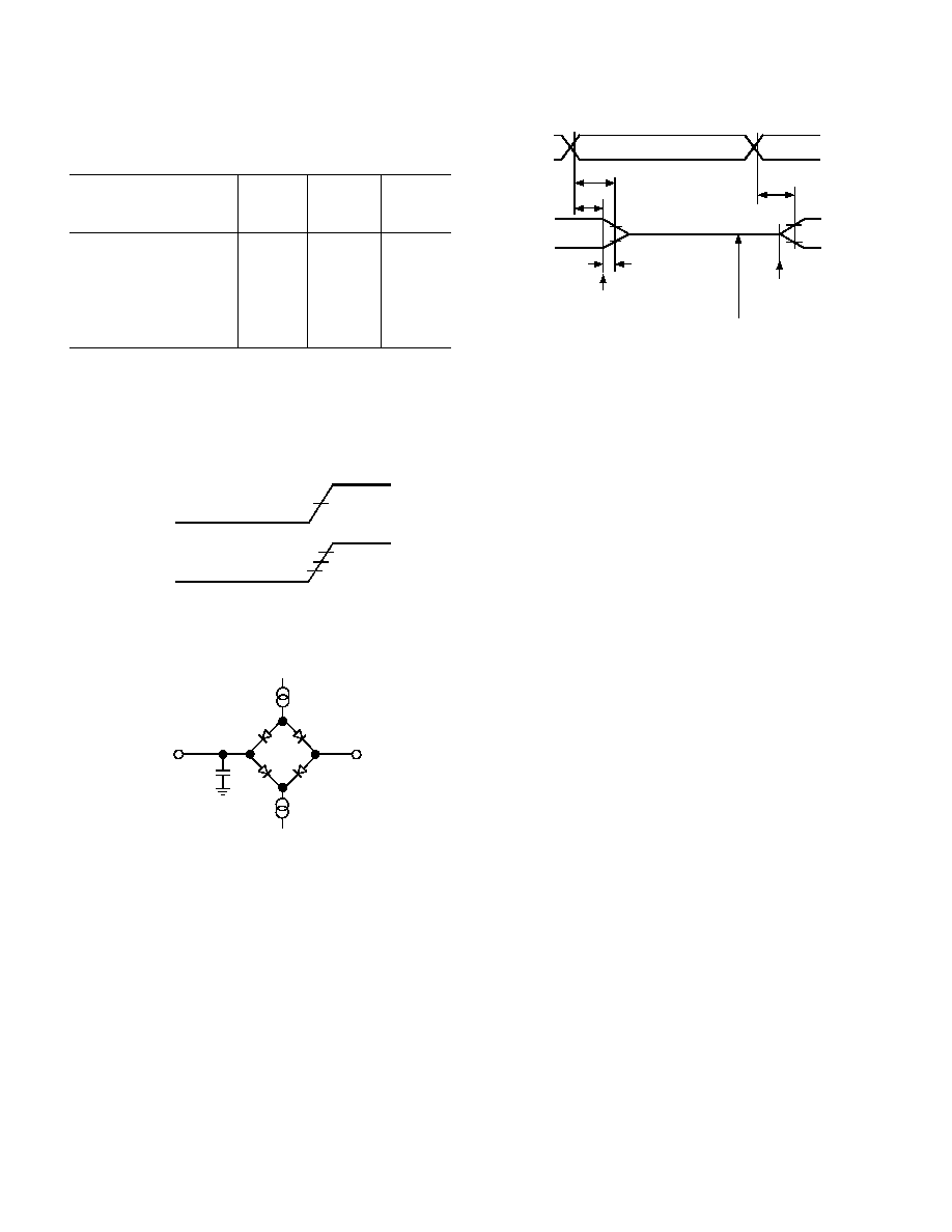
ADSP-218xN Series
≠24≠
REV. 0
Environmental Conditions
Test Conditions
Output Disable Time
Output pins are considered to be disabled when they have
stopped driving and started a transition from the measured
output high or low voltage to a high impedance state. The
output disable time (t
DIS
) is the difference of t
MEASURED
and
t
DECAY
, as shown in
Figure 18
. The time is the interval from
when a reference signal reaches a high or low voltage level
to when the output voltages have changed by 0.5 V from the
measured output high or low voltage.
The decay time, t
DECAY
, is dependent on the capacitive load,
C
L
, and the current load, i
L
, on the output pin. It can be
approximated by the following equation:
from which
is calculated. If multiple pins (such as the data bus) are
disabled, the measurement value is that of the last pin to
stop driving.
Output Enable Time
Output pins are considered to be enabled when they have
made a transition from a high-impedance state to when they
start driving. The output enable time (t
ENA
) is the interval
from when a reference signal reaches a high or low voltage
level to when the output has reached a specified high or low
trip point, as shown in
Figure 18
. If multiple pins (such as
the data bus) are enabled, the measurement value is that of
the first pin to start driving.
Table 14. Thermal Resistance
Rating Description
1
1
Where the Ambient Temperature Rating (T
AMB
) is:
T
AMB
= T
CASE
≠ (PD ◊
CA
)
T
CASE
= Case Temperature in
į
C
PD = Power Dissipation in W
Symbol
LQFP
(
į
C/W)
Mini-
BGA
(
į
C/W)
Thermal Resistance
(Case-to-Ambient)
CA
48
63.3
Thermal Resistance
(Junction-to-Ambient)
JA
50
70.7
Thermal Resistance
(Junction-to-Case)
JC
2
7.4
Figure 16. Voltage Reference Levels for AC
Measurements (Except Output Enable/Disable)
Figure 17. Equivalent Loading for AC Measurements
(Including All Fixtures)
1.5V
OUTPUT
INPUT
1.5V
2.0V
0.8V
TO
OUTPUT
PIN
50pF
1.5V
I
O H
I
OL
Figure 18. Output Enable/Disable
2.0V
1.0V
t
ENA
REFERENCE
SIGNAL
OUTPUT
t
DECAY
V
OH
(MEASURED)
OUTPUT STOPS
DRIVING
OUTPUT STARTS
DRIVING
t
DIS
t
MEASURED
V
OL
(MEASURED)
V
OH
(MEASURED) ≠ 0.5V
V
OL
(MEASURED) + 0.5V
HIGH-IMPEDANCE STATE. TEST CONDITIONS CAUSE
THIS VOLTAGE LEVEL TO BE APPROXIMATELY 1.5V.
V
OH
(MEASURED)
V
OL
(MEASURED)
t
DECAY
C
L
0.5V
◊
i
L
-------------------------
=
t
DIS
t
M EASUR ED
t
DECAY
≠
=
≠25≠
REV. 0
ADSP-218xN Series
TIMING SPECIFICATIONS
This section contains timing information for the DSP's
external signals.
General Notes
Use the exact timing information given. Do not attempt to
derive parameters from the addition or subtraction of
others. While addition or subtraction would yield meaning-
ful results for an individual device, the values given in this
data sheet reflect statistical variations and worst cases. Con-
sequently, parameters cannot be added up meaningfully to
derive longer times.
Timing Notes
Switching characteristics specify how the processor changes
its signals. Designers have no control over this timing--
circuitry external to the processor must be designed for
compatibility with these signal characteristics. Switching
characteristics tell what the processor will do in a given
circumstance. Switching characteristics can also be used to
ensure that any timing requirement of a device connected
to the processor (such as memory) is satisfied.
Timing requirements apply to signals that are controlled by
circuitry external to the processor, such as the data input
for a read operation. Timing requirements guarantee that
the processor operates correctly with other devices.
Frequency Dependency For Timing Specifications
t
CK
is defined as 0.5 t
CKI
. The ADSP-218xN uses an input
clock with a frequency equal to half the instruction rate. For
example, a 40 MHz input clock (which is equivalent to
25 ns) yields a 12.5 ns processor cycle (equivalent to
80 MHz). t
CK
values within the range of 0.5 t
CKI
period
should be substituted for all relevant timing parameters to
obtain the specification value.
Example: t
CKH
= 0.5 t
CK
≠ 2 ns = 0.5 (12.5 ns) ≠ 2 ns= 4.25 ns
Output Drive Currents
Figure 19
shows typical I-V characteristics for the output
drivers on the ADSP-218xN series.The curves represent the
current drive capability of the output drivers as a function
of output voltage.
Figure 21
shows the typical power-down supply current.
Capacitive Loading
Figure 22
and
Figure 23 on page 26
show the capacitive
loading characteristics of the ADSP-218xN.
Figure 19. Typical Output Driver Characteristics
for V
DDEXT
at 3.6 V, 3.3 V, 2.5 V, and 1.8 V
V
OL
SOURCE VOLTAGE ≠ V
0
0.5
1.0
S
O
U
R
C
E
C
U
R
R
E
N
T
≠
m
A
60
0
≠20
≠40
≠60
40
20
V
DDEXT
= 3.6V @ ≠40 C
V
DDEXT
= 3.3V @ +25 C
V
DDEXT
= 1.8/2.5V @ +85 C
V
DDEXT
= 2.5V @ +85 C
V
DDEXT
= 3.6V @ ≠40 C
80
≠80
1.5
2.0
2.5
3.0
3.5
4.0
V
DDEXT
= 1.8/2.5V @ +85 C
V
OH
V
DDEXT
= 3.3V @ +25 C
V
DDEXT
= 1.8V @ +85 C
ADSP-218xN Series
≠26≠
REV. 0
Figure 20. Power vs. Frequency
2.0
P
O
W
E
R
(
P
I
D
L
E
n
)
≠
m
W
8.5mW
3.8mW
3.4mW
4.3mW
10.5mW
POWER, IDLE n MODES
2
1/
t
CK
≠ M Hz
4.0
6.0
8.0
10.0
12.0
0.0
5.0
P
O
W
E
R
(
P
I
D
L
E
)
≠
m
W
POW ER, IDLE
1, 2, 4
1/
t
CK
≠ M Hz
6.0
7.0
8.0
9.0
10.0
11.0
1/
t
CK
≠ M Hz
60
55
POW ER, INT ERNAL
1, 2, 3
P
O
W
E
R
(
P
I
N
T
)
≠
m
W
20
65
70
75
80
85
35
40
45
50
55
60
25
30
NOT ES
VALID F OR ALL TEM PERATURE GRADES.
POW ER R EF LEC TS D EVIC E O PERATING WITH NO OUT PUT
LOAD S.
TYPICAL POWER D ISSIPATION AT 1.8V O R 1.9V V
DDINT
AND
25įC, EXCEPT WHER E SPECIFIED.
I
DD
MEASUREM ENT TAKEN W ITH ALL INST RUCT IONS
EXECU TING FROM INTERNAL M EMO RY. 50% O F THE
INSTRUCTIONS ARE MU LTIFUNCTION (TYPES 1, 4, 5, 12, 13,
14), 30% ARE TYPE 2 AND TYPE 6, AND 20% ARE IDLE
INSTRUCT IONS.
IDL E R EF ERS T O STATE OF OPER ATION DURIN G EXECUTIO N
OF IDLE INSTRUCTION. DEASSERT ED PINS ARE DRIVEN TO
EIT HER V
DD
OR G ND.
1
2
3
4
42 m W
55 m W
V
DD I
NT
= 2
.0V
50 mW
V
D D
INT
= 1
.9V
38 mW
34 mW
45 m W
V
DD IN
T
= 1.
8V
30 mW
40 mW
V
D DIN
T
=
1. 7
1V
60
55
65
70
75
80
85
12.0
13.0
14.0
15.0
10 . 5 m W
13 . 5 m W
V
D D
INT
= 2
.0 V
12 m W
V
DD IN
T
= 1.9
V
9 . 5 m W
8 .5 m W
10 .5 m W
V
DD IN
T
= 1.8
V
7 .5 m W
9m W
V
D DINT
= 1.71
V
60
55
65
70
75
80
85
4.9mW
4.2mW
4.7mW
5.2mW
12.0mW
9.5mW
V
D D
C O R E = 1 . 9 V
V
D D
C O R E = 1 . 8 V
Figure 21. Typical Power-Down Current
Figure 22. Typical Output Rise Time vs. Load Capacitance
(at Maximum Ambient Operating Temperature)
Figure 23. Typical Output Valid Delay or Hold vs. Load
Capacitance, C
L
(at Maximum Ambient Operating
Temperature)
NOTES
1. REFLECTS ADSP-218xN OPERATION IN LOWEST POWER
MODE. (SEE THE "SYSTEM INTERFACE" CHAPTER OF THE
ADSP-218x DSP HARDWARE REFERENCE FOR DETAILS.)
2. CURRENT REFLECTS DEVICE OPERATING WITH NO
INPUT LOADS.
V
DD
= 2.0V
V
DD
= 1.9V
V
DD
= 1.8V
V
DD
= 1.7V
TEMPERATURE ≠ įC
1000
100
0
0
85
25
55
10
C
U
R
R
E
N
T
(
L
O
G
S
C
A
L
E
)
≠
Ķ
A
C
L
≠ pF
R
I
S
E
T
I
M
E
(
0
.
4
V
≠
2
.
4
V
)
≠
n
s
30
300
0
50
100
150
200
250
25
15
10
5
0
20
T = 85 C
V
DD
= 0V TO 2.0V
C
L
≠ pF
14
0
V
A
L
I
D
O
U
T
P
U
T
D
E
L
A
Y
O
R
H
O
L
D
≠
n
s
50
100
150
250
200
12
4
2
≠2
10
8
NOMINAL
16
18
6
≠4
≠6
≠27≠
REV. 0
ADSP-218xN Series
Clock Signals and Reset
Table 15. Clock Signals and Reset
Parameter
Min Max Unit
Timing Requirements:
t
CKI
CLKIN Period
25
40
ns
t
CKIL
CLKIN Width Low
8
ns
t
CKIH
CLKIN Width High
8
ns
Switching Characteristics:
t
CKL
CLKOUT Width Low
0.5t
CK
≠ 3
ns
t
CKH
CLKOUT Width High
0.5t
CK
≠ 3
ns
t
CKOH
CLKIN High to CLKOUT High
0
8
ns
Control Signals Timing Requirements:
t
RSP
RESET Width Low
5t
CK
1
ns
t
MS
Mode Setup before RESET High
7
ns
t
MH
Mode Hold after RESET High
5
ns
1
Applies after power-up sequence is complete. Internal phase lock loop requires no more than 2000 CLKIN cycles, assuming stable CLKIN (not including
crystal oscillator start-up time).
Figure 24. Clock Signals and Reset
t
CKOH
t
CKI
t
CKIH
t
CKIL
t
CKH
t
CKL
t
MH
t
MS
CLKIN
CLKOUT
MODE A D
RESET
t
RSP
ADSP-218xN Series
≠28≠
REV. 0
Interrupts and Flags
Table 16. Interrupts and Flags
Parameter
Min Max Unit
Timing Requirements:
t
IFS
IRQx, FI, or PFx Setup before CLKOUT Low
1,
2,
3,
4
0.25t
CK
+ 10
ns
t
IFH
IRQx, FI, or PFx Hold after CLKOUT High
1,
2,
3,
4
0.25t
CK
ns
Switching Characteristics:
t
FOH
Flag Output Hold after CLKOUT Low
5
0.5t
CK
≠ 5
ns
t
FOD
Flag Output Delay from CLKOUT Low
5
0.5t
CK
+ 4
ns
1
If IRQx and FI inputs meet t
IFS
and t
IFH
setup/hold requirements, they will be recognized during the current clock cycle; otherwise the signals will be
recognized on the following cycle. (Refer to "Interrupt Controller Operation" in the Program Control chapter of the ADSP-218x DSP Hardware Reference
for further information on interrupt servicing.)
2
Edge-sensitive interrupts require pulsewidths greater than 10 ns; level-sensitive interrupts must be held low until serviced.
3
IRQx
=
IRQ0
,
IRQ1
,
IRQ2
,
IRQL0
,
IRQL1
,
IRQLE
.
4
PFx = PF0, PF1, PF2, PF3, PF4, PF5, PF6, PF7.
5
Flag Outputs = PFx, FL0, FL1, FL2, FO.
Figure 25. Interrupts and Flags
t
FOD
t
FOH
t
IFH
t
IFS
CLKOUT
FLAG
OUTPUTS
IRQx
FI
PFx
≠29≠
REV. 0
ADSP-218xN Series
Bus Request≠Bus Grant
Table 17. Bus Request≠Bus Grant
Parameter
Min
Max
Unit
Timing Requirements:
t
BH
BR Hold after CLKOUT High
1
0.25t
CK
+ 2
ns
t
BS
BR Setup before CLKOUT Low
1
0.25t
CK
+ 8
ns
Switching Characteristics:
t
SD
CLKOUT High to xMS, RD, WR Disable
2
0.25t
CK
+ 8
ns
t
SDB
xMS, RD, WR Disable to BG Low
0
ns
t
SE
BG High to xMS, RD, WR Enable
0
ns
t
SEC
xMS, RD, WR Enable to CLKOUT High
0.25t
CK
≠ 3
ns
t
SDBH
xMS, RD, WR Disable to BGH Low
3
0
ns
t
SEH
BGH High to xMS, RD, WR Enable
3
0
ns
1
BR is an asynchronous signal. If BR meets the setup/hold requirements, it will be recognized during the current clock cycle; otherwise the signal will be
recognized on the following cycle. Refer to the ADSP-2100 Family User's Manual for BR/BG cycle relationships.
2
xMS = PMS, DMS, CMS, IOMS, BMS.
3
BGH is asserted when the bus is granted and the processor or BDMA requires control of the bus to continue.
Figure 26. Bus Request≠Bus Grant
CLKOUT
t
SD
t
SDB
t
SE
t
SEC
t
SDBH
t
SEH
t
BS
BR
t
BH
CLKOUT
PMS
,
DMS
BMS
,
RD
CMS
,
WR,
IOMS
BG
BGH
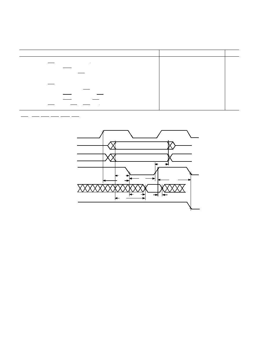
ADSP-218xN Series
≠30≠
REV. 0
Memory Read
Table 18. Memory Read
Parameter
Min
Max
Unit
Timing Requirements:
t
RDD
RD Low to Data Valid
1
1
w = wait states x t
CK
.
0.5t
CK
≠ 5 + w
ns
t
AA
A13 ≠ 0, xMS to Data Valid
2
2
xMS = PMS, DMS, CMS, IOMS, BMS.
0.75t
CK
≠ 6 + w
ns
t
RDH
Data Hold from RD High
0
ns
Switching Characteristics:
t
RP
RD pulsewidth
0.5t
CK
≠ 3 + w
ns
t
CRD
CLKOUT High to RD Low
0.25t
CK
≠ 2
0.25t
CK
+ 4
ns
t
ASR
A13 ≠ 0, xMS Setup before RD Low
0.25t
CK
≠ 3
ns
t
RDA
A13 ≠ 0, xMS Hold after RD Deasserted
0.25t
CK
≠ 3
ns
t
RWR
RD High to RD or WR Low
0.5t
CK
≠ 3
ns
Figure 27. Memory Read
CLKOUT
A0≠A13
D0≠D23
t
RDA
t
RWR
t
RP
t
ASR
t
CRD
t
RDD
t
AA
t
RDH
DMS
,
PMS
,
BMS
,
IOMS
,
CMS
RD
WR
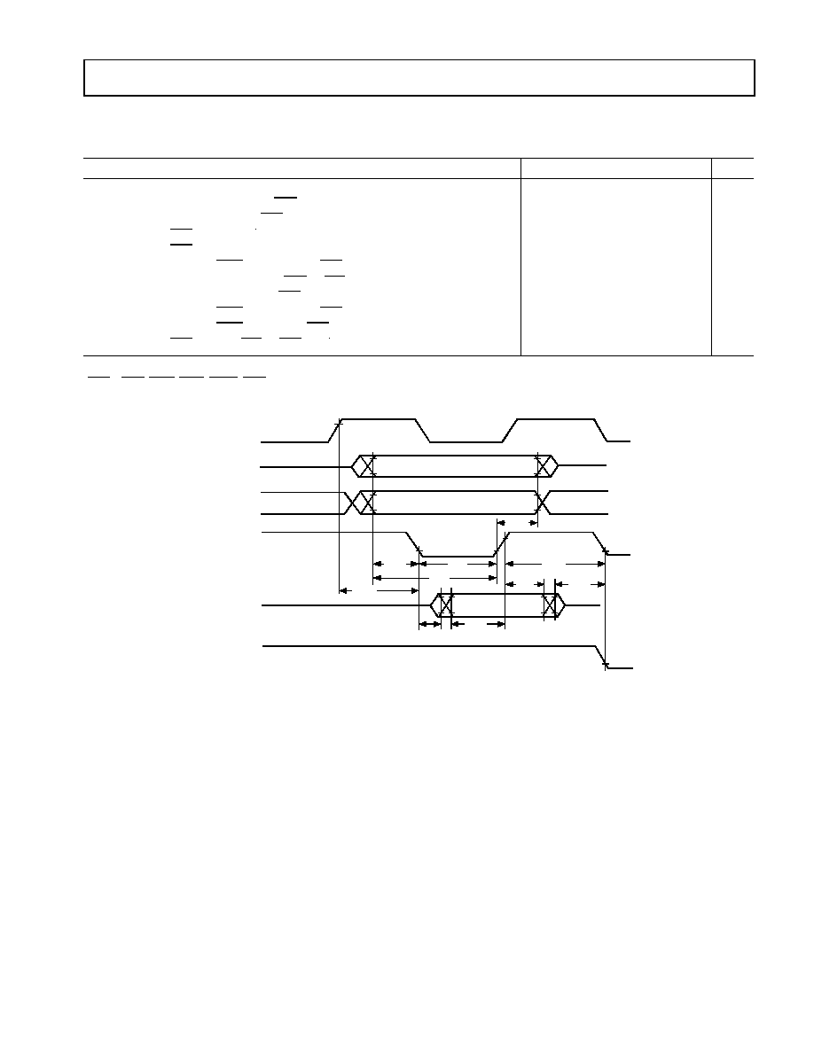
≠31≠
REV. 0
ADSP-218xN Series
Memory Write
Table 19. Memory Write
Parameter
Min
Max
Unit
Switching Characteristics:
t
DW
Data Setup before WR High
1
0.5t
CK
≠ 4 + w
ns
t
DH
Data Hold after WR High
0.25t
CK
≠ 1
ns
t
WP
WR pulsewidth
0.5t
CK
≠ 3 + w
ns
t
WDE
WR Low to Data Enabled
0
ns
t
ASW
A13 ≠ 0, xMS Setup before WR Low
2
0.25t
CK
≠ 3
ns
t
DDR
Data Disable before WR or RD Low
0.25t
CK
≠ 3
ns
t
CWR
CLKOUT High to WR Low
0.25t
CK
≠ 2
0.25t
CK
+ 4
ns
t
AW
A13 ≠ 0, xMS Setup before WR Deasserted
0.75t
CK
≠ 5 + w
ns
t
WRA
A13 ≠ 0, xMS Hold after WR Deasserted
0.25t
CK
≠ 1
ns
t
WWR
WR High to RD or WR Low
0.5t
CK
≠ 3
ns
1
w = wait states t
CK
.
2
xMS = PMS, DMS, CMS, IOMS, BMS.
Figure 28. Memory Write
CLKOUT
A0≠A13
D0≠D23
t
WP
t
AW
t
CWR
t
DH
t
WDE
t
DW
t
ASW
t
WWR
t
WRA
t
DDR
DMS
,
PMS
,
BMS
,
CMS
,
IOMS
RD
WR
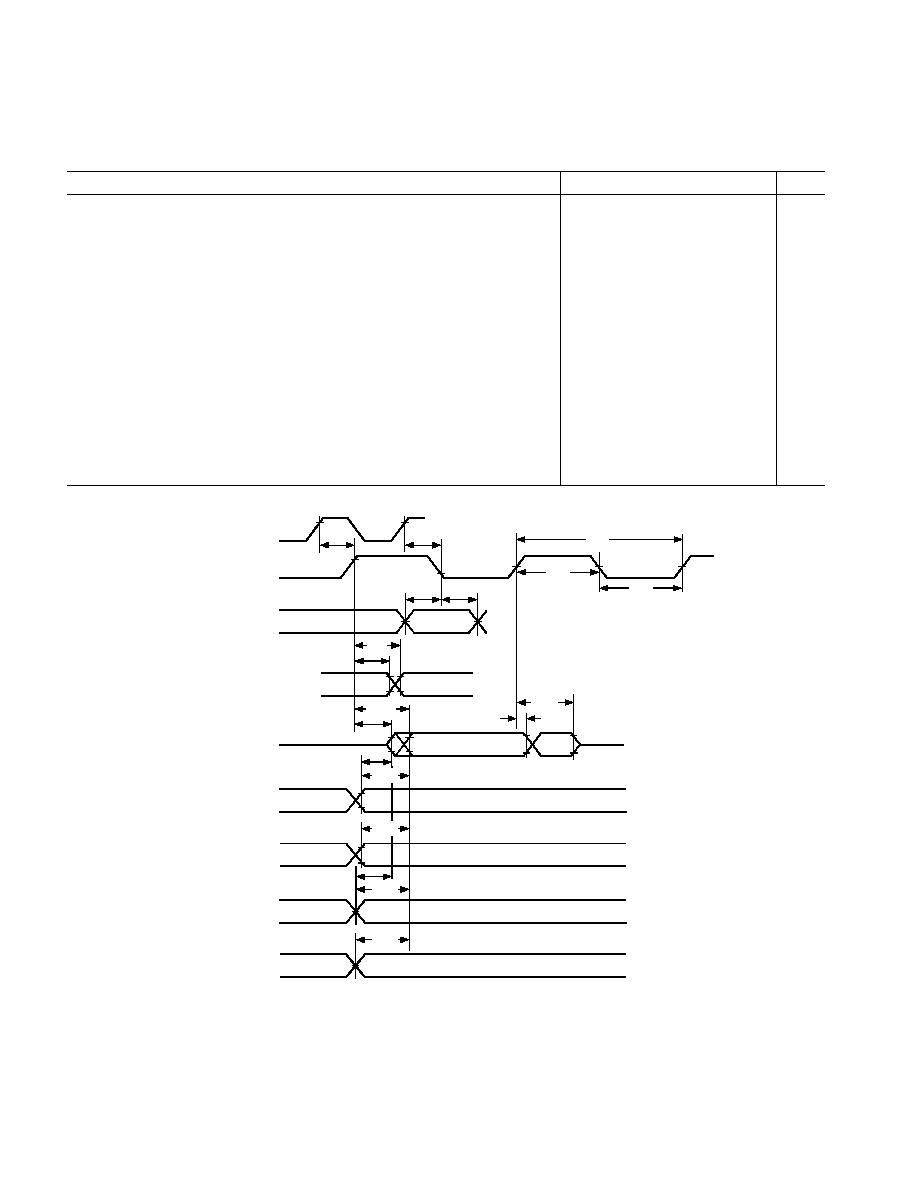
ADSP-218xN Series
≠32≠
REV. 0
Serial Ports
Table 20. Serial Ports
Parameter
Min
Max
Unit
Timing Requirements:
t
SCK
SCLK Period
30
ns
t
SCS
DR/TFS/RFS Setup before SCLK Low
4
ns
t
SCH
DR/TFS/RFS Hold after SCLK Low
7
ns
t
SCP
SCLKIN Width
12
ns
Switching Characteristics:
t
CC
CLKOUT High to SCLKOUT
0.25t
CK
0.25t
CK
+ 6
ns
t
SCDE
SCLK High to DT Enable
0
ns
t
SCDV
SCLK High to DT Valid
12
ns
t
RH
TFS/RFS
OUT
Hold after SCLK High
0
ns
t
RD
TFS/RFS
OUT
Delay from SCLK High
12
ns
t
SCDH
DT Hold after SCLK High
0
ns
t
TDE
TFS (Alt) to DT Enable
0
ns
t
TDV
TFS (Alt) to DT Valid
12
ns
t
SCDD
SCLK High to DT Disable
12
ns
t
RDV
RFS (Multichannel, Frame Delay Zero) to DT Valid
12
ns
Figure 29. Serial Ports
CLKOUT
SCLK
TFS
OUT
RFS
OUT
DT
ALTERNATE
FRAME
MODE
t
C C
t
C C
t
SCS
t
SCH
t
R H
t
SCDE
t
SCDH
t
SCDD
t
TDE
t
RDV
MULTICHANNEL
MODE,
FRAME DELAY 0
(MFD = 0)
DR
TFS
IN
RFS
IN
RFS
OUT
TFS
OUT
t
TDV
t
SCDV
t
R D
t
SCP
t
SCK
TFS
IN
RFS
IN
ALTERNATE
FRAME
MODE
t
RDV
MULTICHANNEL
MODE,
FRAME DELAY 0
(MFD = 0)
t
TDV
t
TDE
t
SCP

≠33≠
REV. 0
ADSP-218xN Series
IDMA Address Latch
Table 21. IDMA Address Latch
Parameter
Min
Max
Unit
Timing Requirements:
t
IALP
Duration of Address Latch
1,
2
10
ns
t
IASU
IAD15 ≠ 0 Address Setup before Address Latch End
2
5
ns
t
IAH
IAD15 ≠ 0 Address Hold after Address Latch End
2
3
ns
t
IKA
IACK Low before Start of Address Latch
2,
3
0
ns
t
IALS
Start of Write or Read after Address Latch End
2,
3
3
ns
t
IALD
Address Latch Start after Address Latch End
1,
2
2
ns
1
Start of Address Latch = IS Low and IAL High.
2
End of Address Latch = IS High or IAL Low.
3
Start of Write or Read = IS Low and IWR Low or IRD Low.
Figure 30. IDMA Address Latch
IACK
IAL
IS
IAD15≠0
IRD
OR
IWR
t
IKA
t
IALP
t
IASU
t
IAH
t
IASU
t
IALS
t
IAH
t
IALP
t
IALD
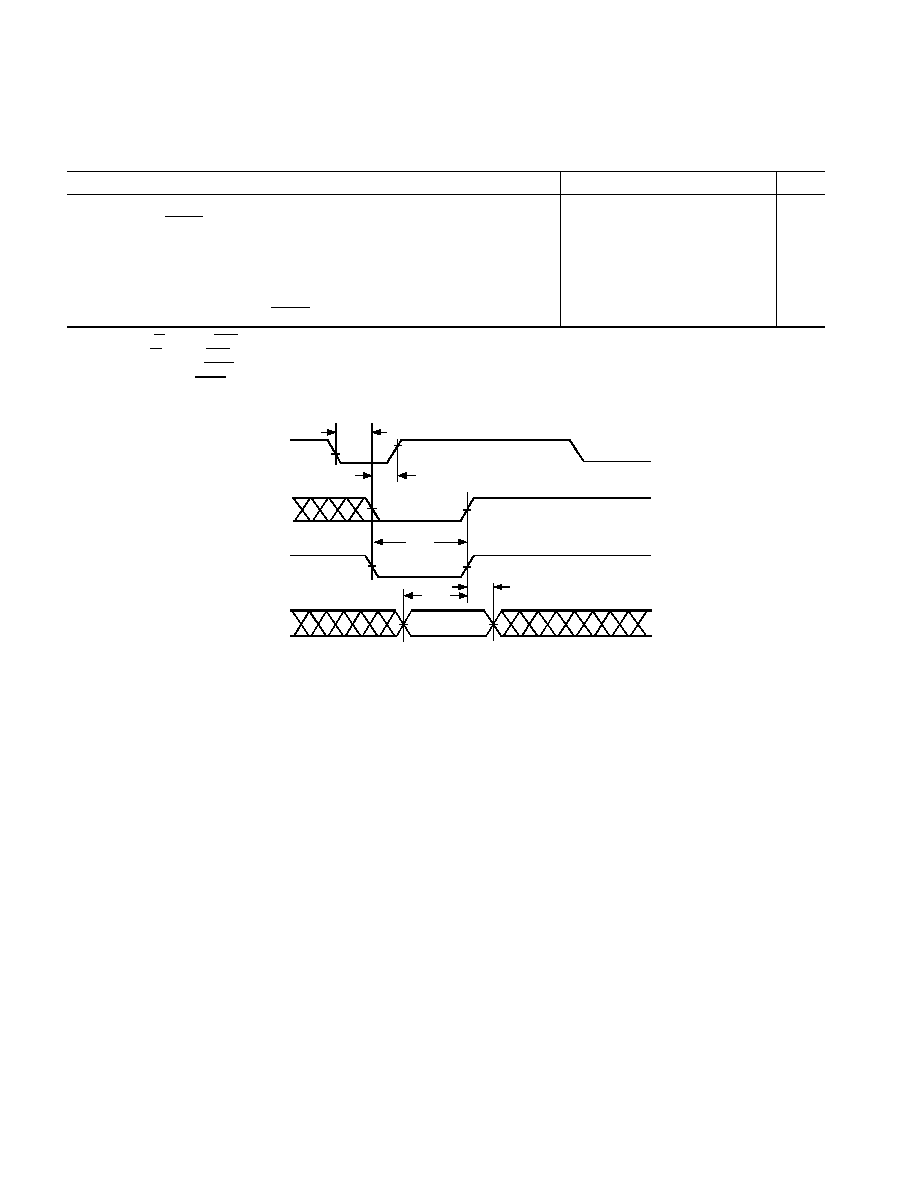
ADSP-218xN Series
≠34≠
REV. 0
IDMA Write, Short Write Cycle
Table 22. IDMA Write, Short Write Cycle
Parameter
Min
Max
Unit
Timing Requirements:
t
IKW
IACK Low before Start of Write
1
0
ns
t
IWP
Duration of Write
1,
2
10
ns
t
IDSU
IAD15 ≠ 0 Data Setup before End of Write
2,
3,
4
3
ns
t
IDH
IAD15 ≠ 0 Data Hold after End of Write
2,
3,
4
2
ns
Switching Characteristic:
t
IKHW
Start of Write to IACK High
10
ns
1
Start of Write = IS Low and IWR Low.
2
End of Write = IS High or IWR High.
3
If Write Pulse ends before IACK Low, use specifications t
IDSU
, t
IDH
.
4
If Write Pulse ends after IACK Low, use specifications t
IKSU
, t
IKH
.
Figure 31. IDMA Write, Short Write Cycle
IAD15≠0
DATA
t
IKHW
t
IKW
t
IDSU
IACK
t
IWP
t
IDH
IS
IWR
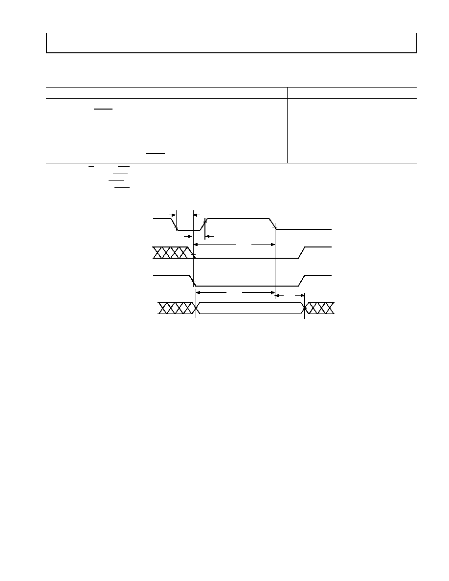
≠35≠
REV. 0
ADSP-218xN Series
IDMA Write, Long Write Cycle
Table 23. IDMA Write, Long Write Cycle
Parameter
Min
Max
Unit
Timing Requirements:
t
IKW
IACK Low before Start of Write
1
0
ns
t
IKSU
IAD15 ≠ 0 Data Setup before End of Write
2,
3,
4
0.5t
CK
+ 5
ns
t
IKH
IAD15 ≠ 0 Data Hold after End of Write
2,
3,
4
0
ns
Switching Characteristics:
t
IKLW
Start of Write to IACK Low
4
1.5t
CK
ns
t
IKHW
Start of Write to IACK High
10
ns
1
Start of Write = IS Low and IWR Low.
2
If Write Pulse ends before IACK Low, use specifications t
IDSU
, t
IDH
.
3
If Write Pulse ends after IACK Low, use specifications t
IKSU
, t
IKH
.
4
This is the earliest time for IACK Low from Start of Write. For IDMA Write cycle relationships, please refer to the ADSP-2100 Family User's Manual.
Figure 32. IDMA Write, Long Write Cycle
IAD15≠0
DATA
t
IKHW
t
IKW
IACK
IS
IWR
t
IKLW
t
IKH
t
IKSU
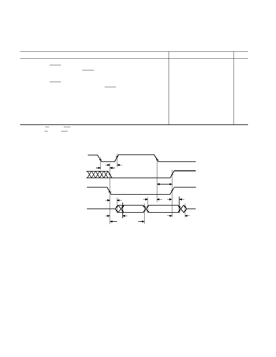
ADSP-218xN Series
≠36≠
REV. 0
IDMA Read, Long Read Cycle
Table 24. IDMA Read, Long Read Cycle
Parameter
Min
Max
Unit
Timing Requirements:
t
IKR
IACK Low before Start of Read
1
0
ns
t
IRK
End of read after IACK Low
2
2
ns
Switching Characteristics:
t
IKHR
IACK High after Start of Read
1
10
ns
t
IKDS
IAD15 ≠ 0 Data Setup before IACK Low
0.5t
CK
≠ 3
ns
t
IKDH
IAD15 ≠ 0 Data Hold after End of Read
2
0
ns
t
IKDD
IAD15 ≠ 0 Data Disabled after End of Read
2
10
ns
t
IRDE
IAD15 ≠ 0 Previous Data Enabled after Start of Read
0
ns
t
IRDV
IAD15 ≠ 0 Previous Data Valid after Start of Read
11
ns
t
IRDH1
IAD15 ≠ 0 Previous Data Hold after Start of Read (DM/PM1)
3
2t
CK
≠ 5
ns
t
IRDH2
IAD15 ≠ 0 Previous Data Hold after Start of Read (PM2)
4
t
CK
≠ 5
ns
1
Start of Read = IS Low and IRD Low.
2
End of Read = IS High or IRD High.
3
DM read or first half of PM read.
4
Second half of PM read.
Figure 33. IDMA Read, Long Read Cycle
t
IRK
t
IKR
PREVIOUS
DATA
READ
DATA
t
iKHR
t
IKDS
t
IRDV
t
iKDD
t
IRDE
t
IKDH
IAD15≠0
IACK
IS
IRD
t
IRDH1 OR
t
IRDH2
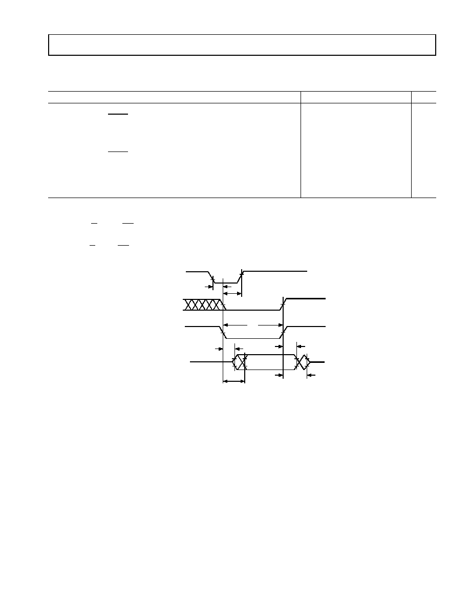
≠37≠
REV. 0
ADSP-218xN Series
IDMA Read, Short Read Cycle
Table 25. IDMA Read, Short Read Cycle
Parameter
1, 2
Min
Max
Unit
Timing Requirements:
t
IKR
IACK Low before Start of Read
3
0
ns
t
IRP1
Duration of Read (DM/PM1)
4
10
2t
CK
≠ 5
ns
t
IRP2
Duration of Read (PM2)
5
10
t
CK
≠ 5
ns
Switching Characteristics:
t
IKHR
IACK High after Start of Read
3
10
ns
t
IKDH
IAD15 ≠ 0 Data Hold after End of Read
6
0
ns
t
IKDD
IAD15 ≠ 0 Data Disabled after End of Read
6
10
ns
t
IRDE
IAD15 ≠ 0 Previous Data Enabled after Start of Read
0
ns
t
IRDV
IAD15 ≠ 0 Previous Data Valid after Start of Read
10
ns
1
Short Read Only must be disabled in the IDMA overlay memory mapped register. This mode is disabled by clearing (= 0) bit 14 of the IDMA overlay
register, and is disabled by default upon reset.
2
Consider using the Short Read Only mode, instead, because Short Read mode is not applicable at high clock frequencies.
3
Start of Read = IS Low and IRD Low.
4
DM Read or first half of PM Read.
5
Second half of PM Read.
6
End of Read = IS High or IRD High.
Figure 34. IDMA Read, Short Read Cycle
t
IRP
t
IKR
PREVIOUS
DATA
t
IKHR
t
iRDV
t
IKDD
t
IRDE
t
IKDH
IAD15≠0
IACK
IS
IRD
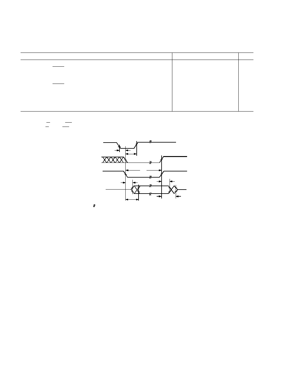
ADSP-218xN Series
≠38≠
REV. 0
IDMA Read, Short Read Cycle in Short Read Only Mode
Table 26. IDMA Read, Short Read Cycle in Short Read Only Mode
Parameter
1
Min
Max
Unit
Timing Requirements:
t
IKR
IACK Low before Start of Read
2
0
ns
t
IRP
Duration of Read
3
10
ns
Switching Characteristics:
t
IKHR
IACK High after Start of Read
2
10
ns
t
IKDH
IAD15 ≠ 0 Previous Data Hold after End of Read
3
0
ns
t
IKDD
IAD15 ≠ 0 Previous Data Disabled after End of Read
3
10
ns
t
IRDE
IAD15 ≠ 0 Previous Data Enabled after Start of Read
0
ns
t
IRDV
IAD15 ≠ 0 Previous Data Valid after Start of Read
10
ns
1
Short Read Only is enabled by setting Bit 14 of the IDMA overlay Register to 1 (0x3FE7). Short Read Only can be enabled by the processor core writing
to the register or by an external host writing to the register. Disabled by default.
2
Start of Read = IS Low and IRD Low. Previous data remains until end of read.
3
End of Read = IS High or IRD High.
Figure 35. IDMA Read, Short Read Cycle in Short Read Only Mode
t
IR P
t
IK R
PR EVIO U S
DA TA
t
IK H R
t
IR D V
t
IK D D
t
IR D E
t
IK D H
IAD 15≠ 0
IACK
IS
IRD
L EG EN D :
IM P L IE S T H A T
IS
A N D
IRD
C A N B E
H EL D IN D E F IN IT EL Y B Y H O ST
≠39≠
REV. 0
ADSP-218xN Series
LQFP Package Pinout
The LQFP package pinout is shown in the illustration below
and in
Table 27
. Pin names in bold text in the table replace
the plain-text-named functions when Mode C = 1. A + sign
separates two functions when either function can be active
for either major I/O mode. Signals enclosed in brackets [ ]
are state bits latched from the value of the pin at the
deassertion of RESET. The multiplexed pins DT1/FO,
TFS1/IRQ1, RFS1/IRQ0, and DR1/FI, are mode
selectable by setting Bit 10 (SPORT1 configure) of the
System Control Register. If Bit 10 = 1, these pins have serial
port functionality. If Bit 10 = 0, these pins are the external
interrupt and flag pins. This bit is set to 1 by default, upon
reset.
100-LEAD LQFP PIN CONFIGURATION
5
4
3
2
7
6
9
8
1
D
1
9
D
1
8
D
1
7
D
1
6
I
R
Q
E
+
P
F
4
I
R
Q
L
0
+
P
F
5
G
N
D
I
R
Q
L
1
+
P
F
6
D
T
0
T
F
S
0
S
C
L
K
0
V
D
D
E
X
T
D
T
1
/
F
O
T
F
S
1
/
I
R
Q
1
D
R
1
/
F
I
G
N
D
S
C
L
K
1
E
R
E
S
E
T
R
E
S
E
T
D15
D14
D13
D12
GND
D11
D10
D9
V
DDEXT
GND
D8
D7/
IWR
D6/
IRD
D5/IAL
D4/
IS
GND
V
DD INT
D3/
IACK
D2/IAD15
D1/IAD14
D0/IAD13
BG
EBG
BR
EBR
A4/IAD3
A5/IAD4
GND
A6/IAD5
A7/IAD6
A8/IAD7
A9/IAD8
A10/IAD9
A11/IAD10
A12/IAD11
A13/IAD12
GND
CLKIN
XTAL
V
DDEXT
CLKOUT
GND
V
DDINT
WR
RD
BMS
DMS
PMS
IOMS
CMS
71
72
73
74
69
70
67
68
65
66
75
60
61
62
63
58
59
56
57
54
55
64
52
53
51
1
0
0
9
9
9
8
9
7
9
6
9
5
9
4
9
3
9
2
9
1
9
0
8
9
8
8
8
7
8
6
8
5
8
4
8
3
8
2
8
1
8
0
7
9
7
8
7
7
7
6
PIN 1
IDENTIFIER
TOP VIEW
(Not to Scale)
2
6
2
7
2
8
2
9
3
0
3
1
3
2
3
3
3
4
3
5
3
6
3
7
3
8
3
9
4
0
4
1
4
2
4
3
4
4
4
5
4
6
4
7
4
8
4
9
5
0
11
10
16
15
14
13
18
17
20
19
22
21
12
24
23
25
ADSP-218xN
I
R
Q
2
+
P
F
7
R
F
S
0
D
R
0
E
M
S
E
E
E
L
O
U
T
E
C
L
K
E
L
I
N
E
I
N
T
A
3
/
I
A
D
2
A
2
/
I
A
D
1
A
1
/
I
A
D
0
A
0
P
W
D
A
C
K
B
G
H
F
L
0
F
L
1
F
L
2
D
2
3
D
2
2
D
2
1
D
2
0
G
N
D
P
F
1
[
M
O
D
E
B
]
G
N
D
P
W
D
V
D
D
E
X
T
P
F
0
[
M
O
D
E
A
]
P
F
2
[
M
O
D
E
C
]
P
F
3
[
M
O
D
E
D
]
R
F
S
1
/
I
R
Q
0
ADSP-218xN Series
≠40≠
REV. 0
Table 27. LQFP Package Pinout
Pin #
Pin Name
1
A4/IAD3
2
A5/IAD4
3
GND
4
A6/IAD5
5
A7/IAD6
6
A8/IAD7
7
A9/IAD8
8
A10/IAD9
9
A11/IAD10
10
A12/IAD11
11
A13/IAD12
12
GND
13
CLKIN
14
XTAL
15
V
DDEXT
16
CLKOUT
17
GND
18
V
DDINT
19
WR
20
RD
21
BMS
22
DMS
23
PMS
24
IOMS
25
CMS
26
IRQE + PF4
27
IRQL0 + PF5
28
GND
29
IRQL1 + PF6
30
IRQ2 + PF7
31
DT0
32
TFS0
33
RFS0
34
DR0
35
SCLK0
36
V
DDEXT
37
DT1/FO
38
TFS1/IRQ1
39
RFS1/IRQ0
40
DR1/FI
41
GND
42
SCLK1
43
ERESET
44
RESET
45
EMS
46
EE
47
ECLK
48
ELOUT
49
ELIN
50
EINT
51
EBR
52
BR
53
EBG
54
BG
55
D0/IAD13
56
D1/IAD14
57
D2/IAD15
58
D3/IACK
59
V
DDINT
60
GND
61
D4/IS
62
D5/IAL
63
D6/IRD
64
D7/IWR
65
D8
66
GND
67
V
DDEXT
68
D9
69
D10
70
D11
71
GND
72
D12
73
D13
74
D14
75
D15
76
D16
77
D17
78
D18
79
D19
80
GND
81
D20
82
D21
83
D22
84
D23
85
FL2
86
FL1
87
FL0
88
PF3 [Mode D]
89
PF2 [Mode C]
90
V
DDEXT
91
PWD
92
GND
93
PF1 [Mode B]
94
PF0 [Mode A]
95
BGH
96
PWDACK
97
A0
98
A1/IAD0
99
A2/IAD1
100
A3/IAD2
Table 27. LQFP Package Pinout (Continued)
Pin #
Pin Name

≠41≠
REV. 0
ADSP-218xN Series
Mini-BGA Package Pinout
The Mini-BGA package pinout is shown in the illustration
below and in
Table 28
. Pin names in bold text in the table
replace the plain text named functions when Mode C = 1.
A + sign separates two functions when either function can
be active for either major I/O mode. Signals enclosed in
brackets [ ] are state bits latched from the value of the pin
at the deassertion of RESET. The multiplexed pins
DT1/FO, TFS1/IRQ1, RFS1/IRQ0, and DR1/FI, are mode
selectable by setting Bit 10 (SPORT1 configure) of the
System Control Register. If Bit 10 = 1, these pins have serial
port functionality. If Bit 10 = 0, these pins are the external
interrupt and flag pins. This bit is set to 1 by default upon
reset.
144-BALL MINI-BGA PACKAGE PINOUT (BOTTOM VIEW)
IRQL 0
+ PF 5
IRQ2
+ P F 7
NC
CMS
GND
D T 1 / F O
DR1/FI
GND
NC
EMS
EE
ECLK
IRQ E
+ PF 4
NC
IRQL 1
+ PF 6
IO M S
GND
PMS
DR0
GND
RESET
EL IN
EL O U T
EINT
NC
NC
NC
BMS
DMS
RFS0
TF S1 /
IRQ1
SCLK1
ERESET
EBR
BR
EBG
CL KOUT
V
D D I N T
NC
V
D D E X T
V
D D E X T
SCLK0
D0/IAD13
RF S1 /
IRQ0
BG
D1/IAD14
V
D D I N T
V
D D I N T
CLKIN
GND
GND
GND
V
D D I N T
DT0
TF S0
D2/IAD15
D3/
IACK
GND
NC
GND
XT A L
NC
GND
A10/IAD9
NC
NC
NC
D6/
IRD
D5 /IAL
NC
NC
D4 /
IS
A13/IAD12
NC
A12/IAD11
A11/IAD10
FL 1
NC
NC
D7 /
IWR
D11
D8
NC
D9
V
D D E X T
V
D D E X T
A8/IAD7
FL 0
PF0
[M OD E A]
FL 2
PF3
[M OD E D]
GND
GND
V
D D E X T
GND
D10
NC
WR
NC
BGH
A9/IAD8
PF1
[M OD E B]
PF2
[M OD E C]
NC
D13
D12
NC
GND
PWDACK
A6/IAD5
RD
A5/IAD4
A7/IAD6
PWD
V
D D E X T
D21
D19
D15
NC
D14
A4/IAD3
A3/IAD2
GND
NC
NC
GND
V
D D E X T
D23
D20
D18
D17
D16
A2/IAD1
A1/IAD0
GND
A0
NC
GND
NC
NC
NC
D22
GND
GND
1
2
3
4
5
6
7
8
9
10
11
12
M
L
K
J
H
G
F
E
D
C
B
A
ADSP-218xN Series
≠42≠
REV. 0
Table 28. Mini-BGA Package Pinout
Ball #
Pin Name
A01
A2/IAD1
A02
A1/IAD0
A03
GND
A04
A0
A05
NC
A06
GND
A07
NC
A08
NC
A09
NC
A10
D22
A11
GND
A12
GND
B01
A4/IAD3
B02
A3/IAD2
B03
GND
B04
NC
B05
NC
B06
GND
B07
V
DDEXT
B08
D23
B09
D20
B10
D18
B11
D17
B12
D16
C01
PWDACK
C02
A6/IAD5
C03
RD
C04
A5/IAD4
C05
A7/IAD6
C06
PWD
C07
V
DDEXT
C08
D21
C09
D19
C10
D15
C11
NC
C12
D14
D01
NC
D02
WR
D03
NC
D04
BGH
D05
A9/IAD8
D06
PF1 [MODE B]
D07
PF2 [MODE C]
D08
NC
D09
D13
D10
D12
D11
NC
D12
GND
E01
V
DDEXT
E02
V
DDEXT
E03
A8/IAD7
E04
FL0
E05
PF0 [MODE A]
E06
FL2
E07
PF3 [MODE D]
E08
GND
E09
GND
E10
V
DDEXT
E11
GND
E12
D10
F01
A13/IAD12
F02
NC
F03
A12/IAD11
F04
A11/IAD10
F05
FL1
F06
NC
F07
NC
F08
D7/IWR
F09
D11
F10
D8
F11
NC
F12
D9
G01
XTAL
G02
NC
G03
GND
G04
A10/IAD9
G05
NC
G06
NC
G07
NC
G08
D6/IRD
G09
D5/IAL
G10
NC
G11
NC
G12
D4/IS
H01
CLKIN
H02
GND
H03
GND
H04
GND
H05
V
DDINT
H06
DT0
H07
TFS0
H08
D2/IAD15
H09
D3/IACK
H10
GND
H11
NC
H12
GND
J01
CLKOUT
J02
V
DDINT
J03
NC
J04
V
DDEXT
J05
V
DDEXT
Table 28. Mini-BGA Package Pinout
(Continued)
Ball #
Pin Name

≠43≠
REV. 0
ADSP-218xN Series
J06
SCLK0
J07
D0/IAD13
J08
RFS1/IRQ0
J09
BG
J10
D1/IAD14
J11
V
DDINT
J12
V
DDINT
K01
NC
K02
NC
K03
NC
K04
BMS
K05
DMS
K06
RFS0
K07
TFS1/IRQ1
K08
SCLK1
K09
ERESET
K10
EBR
K11
BR
K12
EBG
L01
IRQE + PF4
L02
NC
L03
IRQL1 + PF6
L04
IOMS
L05
GND
L06
PMS
L07
DR0
L08
GND
L09
RESET
L10
ELIN
L11
ELOUT
L12
EINT
M01
IRQL0 + PF5
M02
IRQL2 + PF7
M03
NC
M04
CMS
M05
GND
M06
DT1/FO
M07
DR1/FI
M08
GND
M09
NC
M10
EMS
M11
EE
M12
ECLK
Table 28. Mini-BGA Package Pinout
(Continued)
Ball #
Pin Name
ADSP-218xN Series
≠44≠
REV. 0
OUTLINE DIMENSIONS
Dimensions in outline dimension drawings are shown in millimeters.
144-BALL MINI-BGA
(CA-144)
100-LEAD METRIC THIN PLASTIC QUAD FLATPACK (LQFP)
(ST-100)
SEATING
PLANE
1.00
0.85
0.43
0.25
DETAIL A
0.55
0.50
0.45
BALL
DIAMETER
0.10
MAX
DIMENSIONS IN MILLIMETERS .
ACTUAL POSITION OF THE BALL GRID IS
WITHIN 0.15 OF ITS IDEAL POSITION, RELATIVE
TO THE PACKAGE EDGES.
ACTUAL POSITION OF EACH BALL IS WITHIN 0.08
OF ITS IDEAL POSITION, RELATIVE TO THE
BALL GRID.
CENTER DIMENSIONS ARE NOMINAL.
NOTES:
3.
4.
1.
2.
1.40
MAX
DETAIL A
0.80
BSC
BALL
PITCH
8.80
BSC
SQ
A
B
C
D
E
F
G
H
J
K
L
M
12 11 10 9 8 7 6 5 4 3 2 1
10.10
10.00 SQ
9.90
BOTTOM VIEW
TOP VIEW
A1 CO RNER INDEX
TR I AN G LE
SEATING
PLANE
0.75
0.60 TYP
0.50
1.60 MAX
12
T YP
0.15
0.05
6 Ī 4
0 - 7
0.08
MAX LEAD
COPLANARITY
TO P V IEW
(PINS DOWN)
1
25
26
51
50
75
100
76
0.27
0.22 TYP
0.17
16.20
16.00 SQ
15.80
0.50
BSC
12.00 TYP BSC
(LEAD WIDTH)
(LEAD PITCH)
DIMENSIONS IN MILLIMETERS.
THE ACTUAL POSITION OF EACH L EAD IS WITHIN 0.08 OF ITS
IDEAL POSITION, WHEN MEASURED IN THE LATERAL DIRECTION.
CENTER DIMENSIONS ARE NOMINAL.
NOTES:
3.
1.
2.
14.05
14.00 SQ
13.95

≠45≠
REV. 0
ADSP-218xN Series
ORDERING GUIDE
Table 29. Ordering Guide
Part
Number
Ambient
Temperature
Range
Instruction
Rate (MHz)
Package
Description
Package
Option
ADSP-2184NKST-320
0ļC to 70ļC
80
100-Lead LQFP
ST-100
ADSP-2184NBST-320
≠ 40ļC to + 85ļC
80
100-Lead LQFP
ST-100
ADSP-2185NKST-320
0ļC to 70ļC
80
100-Lead LQFP
ST-100
ADSP-2185NBST-320
≠ 40ļC to + 85ļC
80
100-Lead LQFP
ST-100
ADSP-2186NKST-320
0ļC to 70ļC
80
100-Lead LQFP
ST-100
ADSP-2186NBST-320
≠ 40ļC to + 85ļC
80
100-Lead LQFP
ST-100
ADSP-2187NKST-320
0ļC to 70ļC
80
100-Lead LQFP
ST-100
ADSP-2187NBST-320
≠ 40ļC to + 85ļC
80
100-Lead LQFP
ST-100
ADSP-2188NKST-320
0ļC to 70ļC
80
100-Lead LQFP
ST-100
ADSP-2188NBST-320
≠ 40ļC to + 85ļC
80
100-Lead LQFP
ST-100
ADSP-2189NKST-320
0ļC to 70ļC
80
100-Lead LQFP
ST-100
ADSP-2189NBST-320
≠ 40ļC to + 85ļC
80
100-Lead LQFP
ST-100
ADSP-2184NKCA-320
0ļC to 70ļC
80
144-Ball MBGA
CA-144
ADSP-2184NBCA-320
≠ 40ļC to 85ļC
80
144-Ball MBGA
CA-144
ADSP-2185NKCA-320
0ļC to 70ļC
80
144-Ball MBGA
CA-144
ADSP-2185NBCA-320
≠ 40ļC to + 85ļC
80
144-Ball MBGA
CA-144
ADSP-2186NKCA-320
0ļC to 70ļC
80
144-Ball MBGA
CA-144
ADSP-2186NBCA-320
≠ 40ļC to + 85ļC
80
144-Ball MBGA
CA-144
ADSP-2187NKCA-320
0ļC to 70ļC
80
144-Ball MBGA
CA-144
ADSP-2187NBCA-320
≠ 40ļC to + 85ļC
80
144-Ball MBGA
CA-144
ADSP-2188NKCA-320
0ļC to 70ļC
80
144-Ball MBGA
CA-144
ADSP-2188NBCA-320
≠ 40ļC to + 85ļC
80
144-Ball MBGA
CA-144
ADSP-2189NKCA-320
0ļC to 70ļC
80
144-Ball MBGA
CA-144
ADSP-2189NBCA-320
≠ 40ļC to + 85ļC
80
144-Ball MBGA
CA-144

≠46≠

≠47≠

≠48≠
C
0
2
6
6
6
≠
1
≠
1
0
/
0
1
(
0
)
P
R
I
N
T
E
D
I
N
U
.
S
.
A
.