Äîêóìåíòàöèÿ è îïèñàíèÿ www.docs.chipfind.ru
a
DSP Microcomputer
Information furnished by Analog Devices is believed to be accurate and
reliable. However, no responsibility is assumed by Analog Devices for its
use, nor for any infringements of patents or other rights of third parties that
may result from its use. No license is granted by implication or otherwise
under any patent or patent rights of Analog Devices. Trademarks and
registered trademarks are the property of their respective companies.
REV. 0
ADSP-2192M
ADSP-2192M DUAL CORE DSP FEATURES
320 MIPS ADSP-219x DSP in a 144-Lead LQFP Package
with PCI, USB, Sub-ISA, and CardBus Interfaces
3.3 V/5.0 V PCI 2.2 Compliant 33 MHz/32-bit Interface
with Bus Mastering over Four DMA Channels with
Scatter-Gather Support
Integrated USB 1.1 Compliant Interface
Sub-ISA Interface
AC'97 Revision 2.1 Compliant Interface for External
Audio, Modem, and Handset Codecs with DMA
Capability
Dual ADSP-219x Core Processors (P0 and P1) on Each
ADSP-2192M DSP Chip
132K Words of Memory Includes 4K
16-Bit Shared
Data Memory
80K Words of On-Chip RAM on P0, Configured as
64K Words On-Chip 16-Bit RAM for Data Memory and
16K Words On-Chip 24-Bit RAM for Program Memory
48K Words of On-Chip RAM on P1, Configured as
32K Words On-Chip 16-Bit RAM for Data Memory and
16K Words On-Chip 24-Bit RAM for Program Memory
4K Words of Additional On-Chip RAM Shared by Both
Cores, Configured as 4K Words On-Chip 16-Bit RAM
Flexible Power Management with Selectable Power-
Down and Idle Modes
Programmable PLL Supports Frequency Multiplication,
Enabling Full Speed Operation from Low Speed
Input Clocks
2.5 V Internal Operation Supports 3.3 V/5.0 V
Compliant I/O
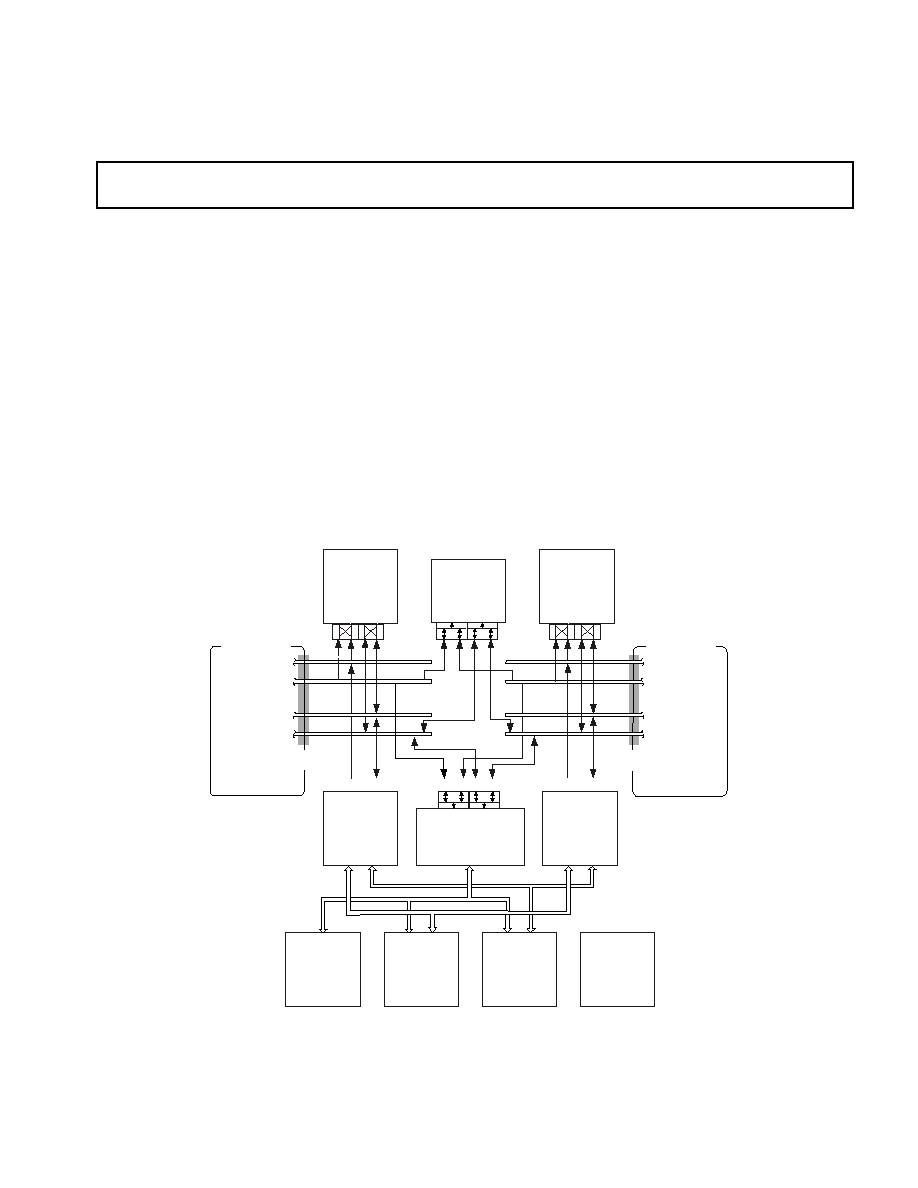
FUNCTIONAL BLOCK DIAGRAM
PROCESSOR P0
CORE
INTERFACE
ADSP-219x
DSP CORE
(SEE FIGURE 1
ON PAGE 3)
SHARED
MEMORY
4K 16 DM
P0
MEMORY
16K 24 PM
64K 16 DM
BOOT ROM
P1
MEMORY
16K 24 PM
32K 16 DM
BOOT ROM
ADDR DATA
P0 DMA
CONTROLLER
FIFOS
SHARED DSP
I/O MAPPED
REGISTERS
P1 DMA
CONTROLLER
FIFOS
HOST PORT
PCI 2.2
OR
USB 1.1
GP I/O PINS
(AND
OPTIONAL
SERIAL
EEPROM)
JTAG
EMULATION
PORT
ADDR DATA
ADDR DATA
ADDR DATA
ADDR DATA
ADDR DATA
SERIAL PORT
AC'97
COMPLIANT
PROCESSOR P1
CORE
INTERFACE
ADSP-219
x
DSP CORE
(SEE FIGURE 1
ON PAGE 3)
One Technology Way, P.O.Box 9106, Norwood, MA 02062-9106, U.S.A.
Tel:781/329-4700
www.analog.com
Fax:781/326-8703
©
2002 Analog Devices, Inc. All rights reserved.

ADSP-2192M
2
REV. 0
ADSP-2192M DUAL CORE DSP FEATURES (continued)
Eight Dedicated General-Purpose I/O Pins with Integrated
Interrupt Support
Each DSP Core Has a Programmable 32-Bit Interval Timer
Five DMA Channels Available on Each Core
Boot Methods Include Booting Through PCI Port, USB
Port, or Serial EEPROM
JTAG Test Access Port Supports On-Chip Emulation and
System Debugging
144-Lead LQFP Package
DSP CORE FEATURES
6.25 ns Instruction Cycle Time (Internal), for up to
160 MIPS Sustained Performance
ADSP-218x Family Code Compatible with the Same Easy
to Use Algebraic Syntax
Single-Cycle Instruction Execution
Dual Purpose Program Memory for Both Instruction and
Data Storage
Fully Transparent Instruction Cache Allows Dual Operand
Fetches in Every Instruction Cycle
Unified Memory Space Permits Flexible Address
Generation, Using Two Independent DAG Units
Independent ALU, Multiplier/Accumulator, and Barrel
Shifter Computational Units with Dual 40-Bit
Accumulators
Single-Cycle Context Switch between Two Sets of
Computational and DAG Registers
Parallel Execution of Computation and Memory
Instructions
Pipelined Architecture Supports Efficient Code Execution
at Speeds up to 160 MIPS
Register File Computations with All Nonconditional,
Nonparallel Computational Instructions
Powerful Program Sequencer Provides Zero-Overhead
Looping and Conditional Instruction Execution
Architectural Enhancements for Compiled C/C++ Code
Efficiency
Architecture Enhancements beyond ADSP-218x Family
are Supported with Instruction Set Extensions for
Added Registers, Ports, and Peripherals
TABLE OF CONTENTS
GENERAL DESCRIPTION . . . . . . . . . . . . . . . . . . . . 3
DSP Core Architecture . . . . . . . . . . . . . . . . . . . . . . . 3
DSP Peripherals . . . . . . . . . . . . . . . . . . . . . . . . . . . . 4
Memory Architecture . . . . . . . . . . . . . . . . . . . . . . . . 4
Interrupts . . . . . . . . . . . . . . . . . . . . . . . . . . . . . . . . . 4
DMA Controller . . . . . . . . . . . . . . . . . . . . . . . . . . . . 6
External Interfaces . . . . . . . . . . . . . . . . . . . . . . . . . . 6
Internal Interfaces . . . . . . . . . . . . . . . . . . . . . . . . . . . 7
Register Spaces . . . . . . . . . . . . . . . . . . . . . . . . . . . . . 7
CardBus Interface . . . . . . . . . . . . . . . . . . . . . . . . . . . 7
Using the PCI Interface . . . . . . . . . . . . . . . . . . . . . . . 7
Using the USB Interface . . . . . . . . . . . . . . . . . . . . . 13
General USB Device Definitions . . . . . . . . . . . . . . . 17
Sub-ISA Interface . . . . . . . . . . . . . . . . . . . . . . . . . . 21
PCI Interface to DSP Memory . . . . . . . . . . . . . . . . 22
USB Interface to DSP Memory . . . . . . . . . . . . . . . . 22
AC'97 Codec Interface to DSP Memory . . . . . . . . . 22
Data FIFO Architecture . . . . . . . . . . . . . . . . . . . . . 22
System Reset Description . . . . . . . . . . . . . . . . . . . . 23
Power Management Description . . . . . . . . . . . . . . . 24
Power Regulators . . . . . . . . . . . . . . . . . . . . . . . . . . 24
2.5 V Regulator Options . . . . . . . . . . . . . . . . . . . . . 24
Low Power Operation . . . . . . . . . . . . . . . . . . . . . . . 25
Clock Signals . . . . . . . . . . . . . . . . . . . . . . . . . . . . . 25
Instruction Set Description . . . . . . . . . . . . . . . . . . . 26
Development Tools . . . . . . . . . . . . . . . . . . . . . . . . . 26
Additional Information . . . . . . . . . . . . . . . . . . . . . . 28
PIN DESCRIPTIONS . . . . . . . . . . . . . . . . . . . . . . . . 28
SPECIFICATIONS . . . . . . . . . . . . . . . . . . . . . . . . . . 30
ABSOLUTE MAXIMUM RATINGS . . . . . . . . . . 31
ESD SENSITIVITY . . . . . . . . . . . . . . . . . . . . . . . . 31
TIMING SPECIFICATIONS . . . . . . . . . . . . . . . . 31
Output Drive Currents . . . . . . . . . . . . . . . . . . . . . . 34
Power Dissipation . . . . . . . . . . . . . . . . . . . . . . . . . . 34
Test Conditions . . . . . . . . . . . . . . . . . . . . . . . . . . . 34
Environmental Conditions . . . . . . . . . . . . . . . . . . . 35
144-Lead LQFP Pinout . . . . . . . . . . . . . . . . . . . . . 36
OUTLINE DIMENSIONS . . . . . . . . . . . . . . . . . . . . 38
ORDERING GUIDE . . . . . . . . . . . . . . . . . . . . . . . . 38
3
REV. 0
ADSP-2192M
GENERAL DESCRIPTION
The ADSP-2192M is a single-chip microcomputer optimized for
digital signal processing (DSP) and other high speed numeric
processing applications, and is ideally suited for PC peripherals.
The ADSP-2192M combines the ADSP-219x family base archi-
tecture (three computational units, two data address generators
and a program sequencer) into a chip with two core processors
(see the Functional Block Diagram
on Page 1
and
Figure 1
).
The ADSP-2192M includes a PCI-compatible port, a USB-
compatible port, an AC'97-compatible port, a DMA controller,
a programmable timer, general-purpose Programmable Flag
pins, extensive interrupt capabilities, and on-chip program and
data memory spaces.
The ADSP-2192M integrates 132K words of on-chip memory
configured as 32K words (24-bit) of program RAM, and 100K
words (16-bit) of data RAM. power-down circuitry is also
provided to reduce power consumption. The ADSP-2192M is
available in a 144-lead LQFP package.
Fabricated in a high speed, low power, CMOS process, the
ADSP-2192M operates with a 6.25 ns instruction cycle time
(320 MIPS) using both cores. All instructions can execute in a
single DSP cycle.
The ADSP-2192M's flexible architecture and comprehensive
instruction set support multiple operations in parallel. For
example, in one processor cycle, each DSP core within the
ADSP-2192M can:
·
Generate an address for the next instruction fetch
·
Fetch the next instruction
·
Perform one or two data moves
·
Update one or two data address pointers
·
Perform a computational operation
These operations take place while the processor continues to:
·
Receive and/or transmit data through the Host port (PCI
or USB interfaces)
·
Receive or transmit data through the AC'97
·
Decrement the two timers
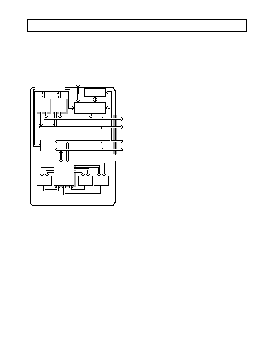
DSP Core Architecture
The ADSP-219x architecture is code compatible with the ADSP-
218x DSP family. Though the architectures are compatible, the
ADSP-219x architecture has many enhancements over the
ADSP-218x architecture. The enhancements to computational
units, data address generators, and program sequencer make the
ADSP-219x more flexible and more compiler friendly.
Indirect addressing options provide addressing flexibility: base
address registers for easier implementation of circular buffering,
pre-modify with no update, post-modify with update, pre- and
post-modify by an immediate 8-bit, twos-complement value.
The ADSP-219x instruction set provides flexible data moves and
multifunction (one or two data moves with a computation)
instructions. Every single-word instruction can be executed in a
single processor cycle. The ADSP-219x assembly language uses
an algebraic syntax for ease of coding and readability. A compre-
hensive set of development tools supports program development.
The Functional Block Diagram
on Page 1
shows the architecture
of the ADSP-219x dual core DSP, while the block diagram of
Figure 1
illustrates the ADSP-219x DSP core. Each core
contains three independent computational units: the multi-
plier/accumulator (MAC), the ALU, and the shifter. The
computational units process 16-bit data from the register file and
have provisions to support multiprecision computations. The
ALU performs a standard set of arithmetic and logic operations;
division primitives are also supported. The MAC performs
single-cycle multiply, multiply/add, and multiply/subtract oper-
ations. The MAC has two 40-bit accumulators that help with
overflow. The shifter performs logical and arithmetic shifts, nor-
malization, denormalization, and derive exponent operations.
The shifter can be used to efficiently implement numeric format
control, including multiword and block floating-point
representations.
Register-usage rules influence placement of input and results
within the computational units. For most operations, the com-
putational units' data registers act as a data register file,
permitting any input or result register to provide input to any unit
for a computation. For feedback operations, the computational
units let the output (result) of any unit be input to any unit on
Figure 1. ADSP-219x DSP Core
CACHE
64
24-BIT
PM ADDRESS BUS
DM ADDRESS BUS
PM DATA BUS
DM DATA BUS
BUS
CONNECT
(PX)
24
16
DSP CORE
PROGRAM
SEQUENCER
DATA
REGISTER
FILE
MULT
BARREL
SHIFTER
ALU
INPUT
REGISTERS
RESULT
REGISTERS
16
16-BIT
CORE
INTERFACE
DAG1
4
4
16
24
24
DAG2
4
4
16

ADSP-2192M
4
REV. 0
the next cycle. For conditional or multifunction instructions,
there are restrictions on which data registers may provide inputs
or receive results from each computational unit. For more infor-
mation, see the ADSP-219x DSP Instruction Set Reference.
A powerful program sequencer controls the flow of instruction
execution. The sequencer supports conditional jumps, subrou-
tine calls, and low interrupt overhead. With internal loop
counters and loop stacks, the ADSP-219x core executes looped
code with zero overhead; no explicit jump instructions are
required to maintain loops.
Two data address generators (DAGs) provide addresses for
simultaneous dual operand fetches. Each DAG maintains and
updates four 16-bit address pointers. Whenever the pointer is
used to access data (indirect addressing), it is pre- or post-
modified by the value of one of four possible modify registers. A
length value and base address may be associated with each pointer
to implement automatic modulo addressing for circular buffers.
Page registers in the DAGs allow linear or circular addressing
within 64K word boundaries of each of the memory pages, but
these buffers may not cross page boundaries. Secondary registers
duplicate all the primary registers in the DAGs; switching
between primary and secondary registers provides a fast context
switch.
Efficient data transfer in the core is achieved with the use of
internal buses:
·
Program Memory Address (PMA) Bus
·
Program Memory Data (PMD) Bus
·
Data Memory Address (DMA) Bus
·
Data Memory Data (DMD) Bus
Program memory can store both instructions and data, permit-
ting the ADSP-219x to fetch two operands in a single cycle, one
from program memory and one from data memory. The DSP's
dual memory buses also let the ADSP-219x core fetch an operand
from data memory and the next instruction from program
memory in a single cycle.
DSP Peripherals
The Functional Block Diagram on Page 1 shows the DSP's
on-chip peripherals, which include the Host port (PCI or USB),
AC'97 port, JTAG test and emulation port, flags, and interrupt
controller.
The ADSP-2192M can respond to up to thirteen interrupts at
any given time. A list of these interrupts appears in
Table 2
.
The AC'97 Codec port on the ADSP-2192M provides a
complete synchronous, full-duplex serial interface. This interface
supports the AC'97 standard.
The ADSP-2192M provides up to eight general-purpose I/O pins
that are programmable as either inputs or outputs. These pins
are dedicated general-purpose Programmable Flag pins.
The programmable interval timer generates periodic interrupts.
A 16-bit count register (TCOUNT) is decremented every
n cycles where n-1 is a scaling value stored in a 16-bit register
(TSCALE). When the value of the count register reaches zero,
an interrupt is generated and the count register is reloaded from
a 16-bit period register (TPERIOD).
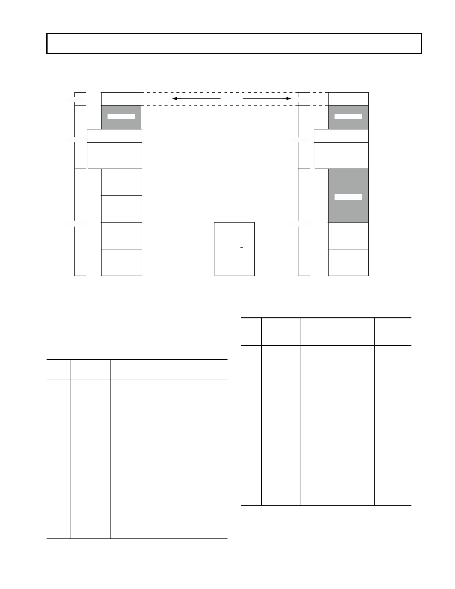
Memory Architecture
The ADSP-2192M provides 132K words of on-chip SRAM
memory. This memory is divided into Program and Data
Memory blocks in each DSP's memory map. In addition to the
internal memory space, the two cores can address two additional
and separate off-core memory spaces: I/O space and shared
memory space, as shown in
Figure 2
.
The ADSP-2192M's two cores can access 80K and 48K locations
that are accessible through two 24-bit address buses, the PMA
and DMA buses.The DSP has three functions that support access
to the full memory map.
·
The DAGs generate 24-bit addresses for data fetches from
the entire DSP memory address range. Because DAG
index (address) registers are 16 bits wide and hold the
lower 16 bits of the address, each of the DAGs has its own
8-bit page register (DMPGx) to hold the most significant
eight address bits. Before a DAG generates an address,
the program must set the DAG's DMPGx register to the
appropriate memory page.
·
The Program Sequencer generates the addresses for
instruction fetches. For relative addressing instructions,
the program sequencer bases addresses for relative jumps,
calls, and loops on the 24-bit Program Counter (PC). In
direct addressing instructions (two-word instructions),
the instruction provides an immediate 24-bit address
value. The PC allows linear addressing of the full 24-bit
address range.
·
For indirect jumps and calls that use a 16-bit DAG
address register for part of the branch address, the
Program Sequencer relies on an 8-bit Indirect Jump page
(IJPG) register to supply the most significant eight
address bits. Before a cross page jump or call, the program
must set the program sequencer's IJPG register to the
appropriate memory page.
Each ADSP-219x DSP core has an on-chip ROM that holds boot
routines (
See Booting Modes on Page 23.
).
Interrupts
The interrupt controller lets the DSP respond to 13 interrupts
with minimum overhead. The controller implements an interrupt
priority scheme as shown in
Table 2
. Applications can use the
unassigned slots for software and peripheral interrupts. The
DSP's Interrupt Control (ICNTL) register (shown in
Table 3
)
provides controls for global interrupt enable, stack interrupt con-
figuration, and interrupt nesting.
5
REV. 0
ADSP-2192M
Table 2
shows the interrupt vector and DSP-to-DSP semaphores
at reset of each of the peripheral interrupts. The peripheral inter-
rupt's position in the IMASK and IRPTL register and its vector
address depend on its priority level, as shown in
Table 2
.
Figure 2. ADSP-2192M Internal/External Memory, Boot Memory, and I/O Memory Maps
SHARED RAM
(16
4K)
DATA RAM
BLO CK3
(16
16K)
DATA RAM
BLO CK2
(16
16K)
DATA RAM
BLO CK1
(16
16K)
RESERVED
0x00 0000
0x00 3FFF
0x00 4000
0x00 8000
0x00 C000
0x01 0000
0x01 4FFF
0x01 5000
0x01 FFFF
ADDRESS
DATA RAM
BLO CK0
(16
16K)
0x00 7FFF
0x00 BFFF
0x00 FFFF
PROG RAM RAM
(24
16K)
PROGRAM RO M
24
4K
0x01 3FFF
0x01 4000
0x02 0000
0x02 0FFF
DSP P0
MEMORY MAP
PAGE 2
PAGE 1
PAGE 0
SHARED
DSP I/O
MAPPED
REGISTERS
PAGES 0 255
(16
256)
0x00 00
0xFF FF
ADDRESS
SHARED RAM
(16
4K)
DATA RAM
BLO CK1
(16
16K)
RESERVED
0x00 0000
0x00 3FF F
0x00 4000
0x00 8000
0x01 0000
0x01 4FF F
0x01 5000
0x01 FFFF
ADDRESS
DATA RAM
BLO CK0
(16
16K)
0x00 7FF F
0x00 FFFF
PROG RAM RAM
(24
16K)
PROGRAM ROM
24
4K
0x01 3FF F
0x01 4000
0x02 0000
0x02 0FF F
DSP P1
MEMORY MAP
RESERVED
PAGE 2
PAGE 1
PAGE 0
SAME
Table 1. DSP-to-DSP Semaphores Register Table
Flag
Bit
Direction
Function
0
Output
DSPDSP Semaphore 0
1
Output
DSPDSP Semaphore 1
2
Output
DSPDSP Interrupt
3
Reserved
4
Reserved
5
Reserved
6
Reserved
7
Output
Register Bus Lock
8
Input
DSPDSP Semaphore 0
9
Input
DSPDSP Semaphore 1
10
Input
DSPDSP Interrupt
11
Input
Reserved
12
Input
AC'97 RegisterPDC Bus Access
Status
13
Input
PDC Interface Busy Status (write
from DSP pending)
14
Input
Reserved
15
Input
Register Bus Lock Status
Table 2. Vector Table
Bit
Priority
Interrupt
Vector
Address
Offset
1
0
1
Reset (non-maskable)
0x00
1
2
Power-Down (non-
maskable)
0x04
2
3
Kernel interrupt
(single step)
0x08
3
4
Stack Status
0x0C
4
5
Mailbox
0x10
5
6
Timer
0x14
6
7
GPIO 0x18
7
8
PCI Bus Master
0x1C
8
9
DSPDSP
0x20
9
10
FIFO0 Transmit
0x24
10
11
FIFO0 Receive
0x28
11
12
FIFO1 Transmit
0x2C
12
13
FIFO1 Receive
0x30
13
14
Reserved
0x34
14
15
Reserved
0x38
15
16
AC'97 Frame
0x3C
1
The interrupt vector address values are represented as offsets from
address 0x01 0000. This address corresponds to the start of Program
Memory in DSP P0 and P1.

ADSP-2192M
6
REV. 0
Interrupt routines can either be nested with higher priority inter-
rupts taking precedence or processed sequentially. Interrupts can
be masked or unmasked with the IMASK register. Individual
interrupt requests are logically ANDed with the bits in IMASK;
the highest priority unmasked interrupt is then selected. The
emulation, power-down, and reset interrupts are nonmaskable
with the IMASK register, but software can use the DIS INT
instruction to mask the power-down interrupt.
The IRPTL register is used to force and clear interrupts. On-chip
stacks preserve the processor status and are automatically main-
tained during interrupt handling. To support interrupt, loop, and
subroutine nesting, the PC stack is 33 levels deep, the loop stack
is eight levels deep, and the status stack is 16 levels deep. To
prevent stack overflow, the PC stack can generate a stack level
interrupt if the PC stack falls below three locations full or rises
above 28 locations full.
The following instructions globally enable or disable interrupt
servicing, regardless of the state of IMASK.
ENA INT;
DIS INT;
At reset, interrupt servicing is disabled.
For quick servicing of interrupts, a secondary set of DAG and
computational registers exist. Switching between the primary
and secondary registers lets programs quickly service interrupts,
while preserving the DSP's state.
DMA Controller
The ADSP-2192M has a DMA controller that supports
automated data transfers with minimal overhead for the DSP
core. Cycle stealing DMA transfers can occur between the
ADSP-2192M's internal memory and any of its DMA-capable
peripherals. DMA transfers can also be accomplished between
any of the DMA-capable peripherals. DMA-capable peripherals
include the PCI and AC'97 ports. Each individual DMA-capable
peripheral has a dedicated DMA channel. DMA sequences do
not contend for bus access with the DSP core; instead, DMAs
"steal" cycles to access memory. All DMA transfers use the
Program Memory (PMA/PMD) buses shown in the Functional
Block Diagram
on Page 1
.
External Interfaces
Several different interfaces are supported on the ADSP-2192M.
These include both internal and external interfaces. The three
separate PCI configuration spaces are programmable to set up
the device in various Plug-and-Play configurations.
The ADSP-2192M provides the following types of external inter-
faces: PCI, USB, Sub-ISA, CardBus, AC'97, and serial
EEPROM. The following sections discuss those interfaces.
PCI 2.2 Host Interface
The ADSP-2192M includes a 33 MHz, 32-bit bus master PCI
interface that is compliant with revision 2.2 of the PCI specifica-
tion. This interface supports the high data rates.
USB 1.1 Host Interface
The ADSP-2192M USB interface enables the host system to
configure and attach a single device with multiple interfaces and
various endpoint configurations. The advantages of this design
include:
·
Programmable descriptors and class-specific command
interpreter.
·
An on-chip 8052-compatible MCU allows the user to soft
download different configurations and support standard
or class-specific commands.
·
Total of eight user-defined endpoints provided.
Endpoints can be configured as either BULK, ISO, or
INT, and the endpoints can be grouped and assigned to
any interface.
Sub-ISA Interface
In systems that combine the ADSP-2192M chip with other
devices on a single PCI interface, the ADSP-2192M Sub-ISA
mode is used to provide a simpler interface that bypasses the
ADSP-2192M's PCI interface. In this mode the Combo Master
assumes all responsibility for interfacing the function to the PCI
bus, including provision of Configuration Space registers for the
ADSP-2192M system as a separate PnP function. In Sub-ISA
Mode the PCI Pins are reconfigured for ISA operation.
CardBus Interface
The CardBus standard provides higher levels of performance
than the 16-bit PC Card standard. For example, 32-bit CardBus
cards are able to take advantage of internal bus speeds that can
be as much as four to six times faster than 16-bit PC Cards. This
design provides for a compact, rugged card that can be completely
inserted within its host computer without any external cabling.
Because CardBus performance attains the same high level as the
host platform's internal (PCI) system bus, it is an excellent way
to add high speed communications to the notebook form factor.
In addition, CardBus PC Cards operate at a power-saving
3.3 volts, extending battery life in most configurations.
This new 32-bit CardBus technology provides up to 132M bytes
per second of bandwidth. This performance makes CardBus an
ideal vehicle to meet the demands of high throughput communi-
cations such as ADSL.
Table 3. Interrupt Control (ICNTL) Register Bits
Bit
Description
03
Reserved
4
Interrupt nesting enable
5
Global interrupt enable
6
Reserved
7
MAC biased rounding enable
89
Reserved
10
PC stack interrupt enable
11
Loop stack interrupt enable
12
Low power idle enable
1315
Reserved

7
REV. 0
ADSP-2192M
CardBus PC Cards generate less heat and consume less power.
This is attained by:
·
Low voltage operation at 3.3 V
·
Software control of clock speed
·
Advanced power management mechanism
AC'97 2.1 External Codec Interface
The industry standard AC'97 serial interface (AC-Link) incor-
porates a 7-pin digital serial interface that links compliant codecs
to the ADSP-2192M. The ACLink implements a bidirectional,
fixed rate, serial PCM digital stream. It handles multiple input
and output audio streams as well as control and status register
accesses using a time division multiplex scheme.
Serial EEPROM Interface
The Serial EEPROM for the ADSP-2192M can overwrite the
following information which is returned during the USB GET
DEVICE DESCRIPTOR command. During the Serial
EEPROM initialization procedure, the DSP is responsible for
writing the USB Descriptor Vendor ID, USB Descriptor Product
ID, USB Descriptor Release Number, and USB Descriptor
Device Attributes registers to change the default settings.
All descriptors can be changed when downloading the RAM-
based MCU renumeration code, except for the Manufacturer
and Product, which are supported in the CONFIG DEVICE and
cannot be overwritten or changed by the Serial EEPROM.
·
Vendor ID (0x0456)
·
Product ID (0x2192)
·
Device Release Number (0x0100)
·
Device Attributes (0x80FA): SP (1 = self-powered,
0 = bus-powered, default = 0); RW (1 = have remote
wake-up capability, 0 = no remote wake-up capability,
default = 0); C[7:0] (power consumption from bus
expressed in 2 mA units; default = 0xFA 500 mA)
·
Manufacturer (ADI)
·
Product (ADI Device)
Internal Interfaces
The ADSP-2192M provides three types of internal interfaces:
registers, codec, and DSP memory buses. The following sections
discuss those interfaces.
Register Interface
The register interface allows the PCI interface, USB interface,
and both DSPs to communicate with the I/O Registers. These
registers map into DSP, PCI, and USB I/O spaces.
Register Spaces
Several different register spaces are defined on the ADSP-
2192M, as described in the following sections.
PCI Configuration Space
These registers control the configuration of the PCI Interface.
Most of these registers are only accessible via the PCI Bus
although a subset is accessible to the DSP for configuration
during the boot.
DSP Core Register Space
Each DSP has an internal register that is accessible with no
latency. These registers are accessible only from within the DSP,
using the REG( ) instruction.
Peripheral Device Control Register Space
This Register Space is accessible by both DSPs, the PCI, Sub-
ISA, and USB Buses. Note that certain sections of this space are
exclusive to either the PCI, USB, or Sub-ISA Buses. These
registers control the operation of the peripherals of the ADSP-
2192M. The DSP accesses these registers using the I/O space
instruction.
USB Register Space
These registers control the operation and configuration of the
USB Interface. Most of these registers are only accessible via the
USB Bus, although a subset is accessible to the DSP.
CardBus Interface
The ADSP-2192M's PC CardBus interface meets the state and
timing specifications defined for PCMCIA's PC CardBus
Standard April 1998 Release 6.1. It supports up to three card
functions. Multiple function PC cards require a separate set of
Configuration registers per function. A primary Card Informa-
tion Structure common to all functions is required. Separate
secondary Card Information Structures, one per function, are
also required. Data for each CIS is loaded by the DSP during
bootstrap loading.
The host PC can read the CIS data at any time. If needed, the
WAIT control can be activated to extend the read operation to
meet bus write access to the CIS data.
Using the PCI Interface
The ADSP-2192M includes a 33 MHz, 32-bit PCI interface to
provide control and data paths between the part and the host
CPU. The PCI interface is compliant with the PCI Local Bus
Specification Revision 2.2. The interface supports bus mastering
as well as bus target interfaces. The PCI Bus Power Management
Interface Specification Revision 1.1 is supported and additional
features as needed by PCI designs are included.
Target/Slave Interface
The ADSP-2192M PCI interface contains three separate func-
tions, each with its own configuration space. Each function
contains four base address registers used to access ADSP-2192M
control registers and DSP memory. Base Address Register
(BAR) 1 is used to point to the control registers. The addresses
specified in these tables are offsets from BAR1 in each of the
functions. PCI memory-type accesses are used to read and write
the registers.
DSP memory accesses use BAR2 or BAR3 of each function.
BAR2 is used to access 24-bit DSP memory; BAR3 accesses
16-bit DSP memory. Maps of the BAR2 and BAR3 registers
appear in
Table 8 on Page 11
and
Table 9 on Page 12
.
The lower half of the allocated space pointed to by each DSP
memory BAR is the DSP memory for DSP core P0. The upper
half is the memory space associated with DSP core P1. PCI
transactions to and from DSP memory use the DMA function
within the DSP core. Thus each word transferred to or from PCI

ADSP-2192M
8
REV. 0
space uses a single DSP clock cycle to perform the internal DSP
data transfer. Byte-wide accesses to DSP memory are not
supported.
I/O type accesses are supported via BAR4. Both the control
registers accessible via BAR1 and the DSP memory accessible
via BAR2 and BAR3 can be accessed with I/O accesses. Indirect
access is used to read and write both the control registers and the
DSP memory. For the control register accesses, an address reg-
ister points to the word to be accessed while a separate register is
used to transfer the data. Read/write control is part of the address
register. Only 16-bit accesses are possible via the I/O space.
A separate set of registers is used to perform the same function
for DSP memory access. Control for these accesses includes a
24-bit/16-bit select as well as direction control. The data register
for DSP memory accesses is a full 24 bits wide. 16-bit accesses
will be loaded into the lower 16 bits of the register.
Table 10 on
Page 14
lists the registers directly accessible from BAR4.
Bus Master Interface
As a bus master, the PCI interface can transfer DMA data
between system memory and the DSP. The control registers for
these transfers are available both to the host and to the DSPs.
Four channels of bus mastering DMA are supported on the
ADSP-2192M.
Two channels are associated with the receive data and two are
associated with the transmit data. The internal DSPs will
typically control initiation of bus master transactions. DMA host
bus master transfers can specify either standard circular buffers
in system memory or perform scatter-gather DMA to host
memory.
Each bus master DMA channel includes four registers to specify
a standard circular buffer in system memory. The Base Address
points to the start of the circular buffer. The Current Address is
a pointer to the current position within that buffer. The Base
Count specifies the size of the buffer in bytes, while the Current
Count keeps track of how many bytes need to be transferred
before the end of the buffer is reached. When the end of the buffer
is reached, the channel can be programmed to loop back to the
beginning and continue the transfers. When this looping occurs,
a Status bit will be set in the DMA Control Register.
The PCI DMA controller can be programmed to perform
scatter-gather DMA, when transferring samples to and from DSP
memory. This mode allows the data to be split up in memory,
and yet be transferable to and from the ADSP-2192M without
processor intervention. In scatter-gather mode, the DMA con-
troller can read the memory address and word count from an
array of buffer descriptors called the Scatter-Gather Descriptor
(SGD) table. This allows the DMA engine to sustain DMA
transfers until all buffers in the SGD table are transferred.
To initiate a scatter-gather transfer between memory and the
ADSP-2192M, the following steps are involved:
1. Software driver prepares a SGD table in system memory.
Each descriptor is eight bytes long and consists of an
address pointer to the starting address and the transfer
count of the memory buffer to be transferred. In any
given SGD table, two consecutive SGDs are offset by
eight bytes and are aligned on a 4-byte boundary. Each
SGD contains:
a. Memory Address (Buffer Start) 4 bytes
b. Byte Count (Buffer Size) 3 bytes
c. End of Linked List (EOL) 1 bit (MSBit)
d.Flag 1 bit (MSBit 1)
2. Initialize DMA control registers with transfer-specific
information such as number of total bytes to transfer,
direction of transfer, etc.
3. Software driver initializes the hardware pointer to the
SGD table.
4. Engage scatter-gather DMA by writing the start value to
the PCI channel Control/Status register.
5. The ADSP-2192M will then pull in samples as pointed
to by the descriptors as needed by the DMA engine.
When the EOL is reached, a status bit will be set and the
DMA will end if the data buffer is not to be looped. If
looping is to occur, DMA transfers will continue from
the beginning of the table until the channel is turned off.
6. Bits in the PCI Control/Status register control whether
an interrupt occurs when the EOL is reached or when
the FLAG bit is set.
Scatter-gather DMA uses four registers. In scatter-gather mode
the functions of the registers are mapped as shown in
Table 4
.
In either mode of operation, interrupts can be generated based
upon the total number of bytes transferred. Each channel has two
24-bit registers to count the bytes transferred and generate inter-
rupts as appropriate. The Interrupt Base Count register specifies
the number of bytes to transfer prior to generating an interrupt.
The Interrupt Count register specifies the current number left
prior to generating the interrupt. When the Interrupt Count
Table 4. Register Mapping in Scatter-Gather Mode
Standard Circular
Buffer Mode
Scatter-Gather Mode
Function
Base Address
SGD Table Pointer
Current Address
SGD Current Pointer
Address
Base Count
SGD Pointer
Current Count
Current SGD Count

9
REV. 0
ADSP-2192M
register reaches zero, a PCI interrupt can be generated. Also, the
Interrupt Count register will be reloaded from the Interrupt Base
Count and continue counting down for the next interrupt.
PCI Interrupts
There are a variety of potential sources of interrupts to the PCI
host besides the bus master DMA interrupts. A single interrupt
pin,
INTA is used to signal these interrupts back to the host. The
PCI Interrupt Register consolidates all of the possible interrupt
sources; the bits of this register are shown in
Table 5
. The register
bits are set by the various sources, and can be cleared by writing
a 1 to the bit(s) to be cleared.
PCI Control Register.
This register must be initialized by the DSP ROM code prior to
PCI enumeration. (It has no effect in ISA or USB mode.) Once
the Configuration Ready bit has been set to 1, the PCI Control
Register becomes read-only, and further access by the DSP to
configuration space is disallowed. The bits of this register are
shown in
Table 6
.
PCI Configuration Space
The ADSP-2192M PCI Interface provides three separate con-
figuration spaces, one for each possible function. This document
describes the registers in each function, their reset condition, and
how the three functions interact to access and control the ADSP-
2192M hardware.
Similarities Between the Three PCI Functions
Each function contains a complete set of registers in the pre-
defined header region as defined in the PCI Local Bus
Specification Revision 2.2. In addition, each function contains
the optional registers to support PCI Bus Power Management.
Generally, registers that are unimplemented or read-only in one
function are similarly defined in the other functions. Each
function contains four base address registers that are used to
access ADSP-2192M control registers and DSP memory.
Base address register (BAR) 1 is used to access the ADSP-
2192M control registers. Accesses to the control registers via
BAR1 uses PCI memory accesses. BAR1 requests a memory
allocation of 1024 bytes. Access to DSP memory occurs via
BAR2 and BAR3. BAR2 is used to access 24-bit DSP memory
(for DSP program downloading) while BAR3 is used to access
16-bit DSP memory. BAR4 provides I/O space access to both the
control registers and the DSP memory.
Table 7
shows the configuration space headers for the three
spaces. While these are the default uses for each of the configu-
rations, they can be redefined to support any possible function
by writing to the class code register of that function during boot.
Additionally, during boot time, the DSP can disable one or more
of the functions. If only two functions are enabled, they will be
functions 0 and 1. If only one function is enabled, it will be
function 0.
Interactions Between the Three PCI Configurations
Because the configurations must access and control a single set
of resources, potential conflicts can occur between the control
specified by the configuration.
Target accesses to registers and DSP memory can go through any
function. As long as the Memory Space access enable bit is set in
that function, then PCI memory accesses whose addresses match
the locations programmed into a function, BARs 13 will be able
to read or write any visible register or memory location within the
ADSP-2192M. Similarly, if I/O space access enable is set, then
PCI I/O accesses can be performed via BAR4.
Within the Power Management section of the configuration
blocks, there are a few interactions. The part will stay in the
highest power state between the three configurations.
Table 5. PCI Interrupt Register
Bit
Name
Comments
0
Reserved
Reserve
1
Rx0 DMA Channel
Interrupt
Receive Channel 0 Bus
Master Transactions
2
Rx1 DMA Channel
Interrupt
Receive Channel 1 Bus
Master Transactions
3
Tx0 DMA Channel
Interrupt
Transmit Channel 0 Bus
Master Transactions
4
Tx1 DMA Channel
Interrupt
Transmit Channel 1 Bus
Master Transactions
5
Incoming Mailbox
0 PCI Interrupt
PCI to DSP Mailbox 0
Transfer
6
Incoming Mailbox
1 PCI Interrupt
PCI to DSP Mailbox 1
Transfer
7
Outgoing Mailbox
0 PCI Interrupt
DSP to PCI Mailbox 0
Transfer
8
Outgoing Mailbox
1 PCI Interrupt
DSP to PCI Mailbox 1
Transfer
9
Reserved
10
Reserved
11
I/O Wake-up
I/O Pin Initiated
12
AC'97 Wake-up
AC'97 Interface Initiated
13
PCI Master Abort
Interrupt
PCI Interface Master Abort
Detected
14
PCI Target Abort
Interrupt
PCI Interface Target Abort
Detected
15
Reserved
Table 6. PCI Control Register
Bit
Name
Comments
10
PCI Functions
Configured
00 = One PCI function
enabled, 01 = Two functions,
10 = Three functions
2
Configuration
Ready
When 0, disables PCI accesses
to the ADSP-2192M (termi-
nated with Retry). Must be set
to 1 by DSP ROM code after
initializing configuration
space. Once 1, cannot be
written to 0.
153
Reserved

ADSP-2192M
10
REV. 0
PCI Memory Map
The ADSP-2192M On-Chip Memory is mapped to the PCI
Address Space. Because some ADSP-2192M Memory Blocks
are 24 bits wide (Program Memory) while others are 16 bits
(Data Memory), two different footprints are available in PCI
Address Space. These footprints are available to each PCI
function by accessing different PCI Base Address Registers
(BAR). BAR2 supports 24-bit "Unpacked" Memory Access.
BAR3 supports 16-bit "Packed" Memory Access.
In 24-bit (BAR2) Mode, each 32 bits (four Consecutive PCI
Byte Address Locations, which make up one PCI Data word)
correspond to a single ADSP-2192M Memory Location. BAR2
Mode is typically used for Program Memory Access. Byte3 is
always unused. Bytes[2:0] are used for 24-bit Memory Locations.
As shown in
Figure 3
, Bytes[2:1] are used for 16-bit Memory
Locations.
In 16-bit (BAR3) Mode (
Figure 4
), each 32-bit (four Consecu-
tive PCI Byte Address Locations) PCI Data Word corresponds
to two ADSP-2192M Memory Locations. Bytes[3:2] contain
one 16-bit Data Word, Bytes[1:0] contain a second 16-bit Data
Word. BAR3 Mode is typically used for Data Memory Access.
Only the 16 MSBs of a Data Word are accessed in 24-bit Blocks;
the 8 LSBs are ignored.
Table 7. PCI Configuration Space 0, 1, and 2
Address
Name
Reset
Comments
0x010x00
Vendor ID
0x11D4
Writable from the DSP during initialization
0x030x02
Config 0 Device ID
0x2192
Writable from the DSP during initialization
Config 1 Device ID
0x219A
Writable from the DSP during initialization
Config 2 Device ID
0x219E
Writable from the DSP during initialization
0x050x04
Command Register
0x0
Bus Master, Memory Space Capable, I/O Space
Capable
0x070x06
Status Register
0x0
Bits enabled: Capabilities List, Fast B2B,
Medium Decode
0x08
Revision ID
0x0
Writable from the DSP during initialization
0x0B0x09
Class Code
0x48000
Writable from the DSP during initialization
0x0C
Cache Line Size
0x0
Read Only
0x0D
Latency Timer
0x0
0x0E
Header Type
0x80
Multifunction bit set
0x0F
BIST
0x0
Unimplemented
0x130x10
Base Address 1
0x08
Register Access for all ADSP-2192M Registers,
Prefetchable Memory
0x170x14
Base Address2
0x08
24-bit DSP Memory Access
0x1B0x18
Base Address3
0x08
16-bit DSP Memory Access
0x1F0x1C
Base Address4
0x01
I/O access for control registers and DSP memory
0x230x20
Base Address5
0x0
Unimplemented
0x270x24
Base Address6
0x0
Unimplemented
0x2B0x28
Config 0 CardBus CIS Pointer
0x1FF03
CIS RAM Pointer - Function 0 (Read Only)
Config 1 CardBus CIS Pointer
0x1FE03
CIS RAM Pointer - Function 1 (Read Only)
Config 2 CardBus CIS Pointer
0x1FD03
CIS RAM Pointer - Function 2 (Read Only)
0x2D0x2C
Subsystem Vendor ID
0x11D4
Writable from the DSP during initialization
0x2F0x2E
Config 0 Subsystem Device ID
0x2192
Writable from the DSP during initialization
Config 1 Subsystem Device ID
0x219A
Writable from the DSP during initialization
Config 2 Subsystem Device ID
0x219E
Writable from the DSP during initialization
0x330x30
Expansion ROM Base Address
0x0
Unimplemented
0x34
Capabilities Pointer
0x40
Read Only
0x3C
Interrupt Line
0x0
0x3D
Interrupt Pin
0x1
Uses
INTA Pin
0x3E
Min_Gnt
0x1
Read Only
0x3F
Max_Lat
0x4
Read Only
0x40
Capability ID
0x1
Power Management Capability Identifier
0x41
Next_Cap_Ptr
0x0
Read Only
0x430x42
Power Management Capabilities
0x6C22
Writable from the DSP during initialization
0x450x44
Power Management Control/Status
0x0
Bits 15 and 8 initialized only on Power-up
0x46
Power Management Bridge
0x0
Unimplemented
0x47
Power Management Data
0x0
Unimplemented
11
REV. 0
ADSP-2192M
24-Bit PCI DSP Memory Map (BAR2)
The complete PCI address footprint for the ADSP-2192M DSP
Memory Spaces in 24-bit (BAR2) Mode is shown in
Table 8
.
Figure 3. PCI Addressing for 24-Bit and 16-Bit Memory Blocks in 24-Bit Access (BAR2) Mode
Figure 4. PCI Addressing for 24-Bit and 16-Bit Memory Blocks in 16-Bit Access (BAR3) Mode
UNUSED
UNUSED
BYTE3
BYTE0
BYTE1
BYTE2
16K
24-BIT BLOCK
16K
16-BIT BLOCK
PCI DWORD
PCI BYTE ADDRESS
DSP WORD ADDRESS
0x0 0000
0x0000
0x1 FFFC
0x1 0000
0x0 FFFC
0x3FFF
0x4000
0x7FFF
BYTE3 IS
ALWAYS
UNUSED
BYTE0 IS UNUSED
BY 16-BIT MEMORY
LOCATIONS
ALLOWED BYTE
ENABLES:
CBE
= 1100
CBE
= 0011
UNUSED
BYTE3
BYTE0
BYTE1
BYTE2
16K
24-BIT BLOCK
16K
16-BIT BLOCK
PCI DWORD
PCI BYTE ADDRESS
DSP WORD ADDRESS
0x0 0000
0x0000
0x0 FFFE
0x0 8000
0x0 7FFE
0x3FFF
0x4000
0x7FFF
ALL BYTES ARE USED.
ALLOWED BYTE
ENABLES:
CBE
= 1100
CBE
= 0011
CBE
= 0000
UNUSED
DATA WORD N + 1
DATA WORD N
DATA WORD N + 1
DATA WORD N
Table 8. 24-Bit PCI DSP Memory Map (BAR2 Mode)
1
Block
Byte3
Byte2
Byte1
Byte0
Offset
DSP P0 Data RAM
Block 0
UNUSED
D[15:8]
D[7:0]
UNUSED
0x0000 0000
UNUSED
D[15:8]
D[7:0]
UNUSED
0x0000 0004
. . .
. . .
. . .
. . .
. . .
UNUSED
D[15:8]
D[7:0]
UNUSED
0x0000 FFFC
DSP P0 Data RAM
Block 1
UNUSED
D[15:8]
D[7:0]
UNUSED
0x0001 0000
UNUSED
D[15:8]
D[7:0]
UNUSED
0x0001 0004
. . .
. . .
. . .
. . .
. . .
UNUSED
D[15:8]
D[7:0]
UNUSED
0x0001 FFFC
DSP P0 Data RAM
Block 2
UNUSED
D[15:8]
D[7:0]
UNUSED
0x0002 0000
UNUSED
D[15:8]
D[7:0]
UNUSED
0x0002 0004
. . .
. . .
. . .
. . .
. . .
UNUSED
D[15:8]
D[7:0]
UNUSED
0x0002 FFFC
DSP P0 Data RAM
Block 3
UNUSED
D[15:8]
D[7:0]
UNUSED
0x0003 0000
UNUSED
D[15:8]
D[7:0]
UNUSED
0x0003 0004
. . .
. . .
. . .
. . .
. . .
UNUSED
D[15:8]
D[7:0]
UNUSED
0x0003 FFFC
DSP P0 Program RAM
Block
UNUSED
D[23:16]
D[15:8]
D[7:0]
0x0004 0000
UNUSED
D[23:16]
D[15:8]
D[7:0]
0x0004 0004
. . .
. . .
. . .
. . .
. . .
UNUSED
D[23:16]
D[15:8]
D[7:0]
0x0004 FFFC

ADSP-2192M
12
REV. 0
16-Bit PCI DSP Memory Map (BAR3)
The complete PCI address footprint for the ADSP-2192M DSP
Memory Spaces in 16-bit (BAR3) Mode is shown in
Table 9
.
DSP P0 Program ROM
Block
UNUSED
D[23:16]
D[15:8]
D[7:0]
0x0005 0000
UNUSED
D[23:16]
D[15:8]
D[7:0]
0x0005 0004
. . .
. . .
. . .
. . .
. . .
UNUSED
D[23:16]
D[15:8]
D[7:0]
0x0005 3FFC
Reserved Space
RESERVED
RESERVED
RESERVED
RESERVED
0x0005 4000
. . .
. . .
. . .
. . .
. . .
RESERVED
RESERVED
RESERVED
RESERVED
0x0007 FFFC
DSP P1 Data RAM
Block 0
UNUSED
D[15:8]
D[7:0]
UNUSED
0x0008 0000
UNUSED
D[15:8]
D[7:0]
UNUSED
0x0008 0004
. . .
. . .
. . .
. . .
. . .
UNUSED
D[15:8]
D[7:0]
UNUSED
0x0008 FFFC
DSP P1 Data RAM
Block 1
UNUSED
D[15:8]
D[7:0]
UNUSED
0x0009 0000
UNUSED
D[15:8]
D[7:0]
UNUSED
0x0009 0004
. . .
. . .
. . .
. . .
. . .
UNUSED
D[15:8]
D[7:0]
UNUSED
0x0009 FFFC
Reserved Space
UNUSED
D[15:8]
D[7:0]
UNUSED
0x000A 0000
UNUSED
D[15:8]
D[7:0]
UNUSED
0x000A 0004
. . .
. . .
. . .
. . .
. . .
UNUSED
D[15:8]
D[7:0]
UNUSED
0x000B FFFC
DSP P1 Program RAM
Block
UNUSED
D[23:16]
D[15:8]
D[7:0]
0x000C 0000
UNUSED
D[23:16]
D[15:8]
D[7:0]
0x000C 0004
. . .
. . .
. . .
. . .
. . .
UNUSED
D[23:16]
D[15:8]
D[7:0]
0x000C FFFC
DSP P1 Program ROM
Block
UNUSED
D[23:16]
D[15:8]
D[7:0]
0x000D 0000
UNUSED
D[23:16]
D[15:8]
D[7:0]
0x000D 0004
. . .
. . .
. . .
. . .
. . .
UNUSED
D[23:16]
D[15:8]
D[7:0]
0x000D 3FFC
Reserved Space
RESERVED
RESERVED
RESERVED
RESERVED
0x000D 4000
. . .
. . .
. . .
. . .
. . .
RESERVED
RESERVED
RESERVED
RESERVED
0x000F FFFC
1
The ". . ." entries in this table indicate the continuation of the pattern shown in the first rows of each section.
Table 8. 24-Bit PCI DSP Memory Map (BAR2 Mode)
1
(continued)
Block
Byte3
Byte2
Byte1
Byte0
Offset
Table 9. 16-Bit PCI DSP Memory Map (BAR3 Mode)
1
Block
Byte3
Byte2
Byte1
Byte0
Offset
DSP P0 Data RAM
Block 0
D[15:8]
D[7:0]
D[15:8]
D[7:0]
0x0000 0000
D[15:8]
D[7:0]
D[15:8]
D[7:0]
0x0000 0004
. . .
. . .
. . .
. . .
. . .
D[15:8]
D[7:0]
D[15:8]
D[7:0]
0x0000 7FFC
DSP P0 Data RAM
Block 1
D[15:8]
D[7:0]
D[15:8]
D[7:0]
0x0000 8000
D[15:8]
D[7:0]
D[15:8]
D[7:0]
0x0000 8004
. . .
. . .
. . .
. . .
. . .
D[15:8]
D[7:0]
D[15:8]
D[7:0]
0x0000 FFFC
DSP P0 Data RAM
Block 2
D[15:8]
D[7:0]
D[15:8]
D[7:0]
0x0001 0000
D[15:8]
D[7:0]
D[15:8]
D[7:0]
0x0001 0004
. . .
. . .
. . .
. . .
. . .
D[15:8]
D[7:0]
D[15:8]
D[7:0]
0x0001 7FFC

13
REV. 0
ADSP-2192M
16-Bit PCI DSP I/O Memory Map (BAR4)
PCI Base Address Register (BAR4) allows indirect access to the
ADSP-2192M Control Registers and DSP Memory. The DSP
Memory Indirect Access Registers accessible from BAR4 are
shown in
Table 10
.
DSP P0 Memory Indirect Address Space occupies PCI BAR4
Space 0x000000 through 0x01FFFF
DSP P1 Memory Indirect Address Space occupies PCI BAR4
Space 0x020000 through 0x03FFFF
All Indirect DSP Memory Accesses are 24-bit or 16-bit Word
Accesses.
Using the USB Interface
The ADSP-2192M USB design enables the ADSP-2192M to be
configured and attached to a single device with multiple inter-
faces and various endpoint configurations, as follows:
1. Programmable descriptors and a class-specific com-
mand interpreter are accessible through the USB 8052
registers. An 8052 compatible MCU is supported
on-board, to enable soft downloading of different config-
urations, and support of standard or class-specific
commands.
2. A total of eight user-defined endpoints are provided.
Endpoints can be configured as BULK, ISO, or INT,
and can be grouped.
DSP P0 Data RAM
Block 3
D[15:8]
D[7:0]
D[15:8]
D[7:0]
0x0001 8000
D[15:8]
D[7:0]
D[15:8]
D[7:0]
0x0001 8004
. . .
. . .
. . .
. . .
. . .
D[15:8]
D[7:0]
D[15:8]
D[7:0]
0x0001 FFFC
DSP P0 Program RAM
Block
D[23:16]
D[15:8]
D[23:16]
D[15:8]
0x0002 0000
D[23:16]
D[15:8]
D[23:16]
D[15:8]
0x0002 0004
. . .
. . .
. . .
. . .
. . .
D[23:16]
D[15:8]
D[23:16]
D[15:8]
0x0002 7FFC
DSP P0 Program ROM
Block
D[23:16]
D[15:8]
D[23:16]
D[15:8]
0x0002 8000
D[23:16]
D[15:8]
D[23:16]
D[15:8]
0x0002 8004
. . .
. . .
. . .
. . .
. . .
D[23:16]
D[15:8]
D[23:16]
D[15:8]
0x0002 9FFC
Reserved Space
RESERVED
RESERVED
RESERVED
RESERVED
0x0002 A000
. . .
. . .
. . .
. . .
. . .
RESERVED
RESERVED
RESERVED
RESERVED
0x0003 FFFC
DSP P1 Data RAM
Block 0
D[15:8]
D[7:0]
D[15:8]
D[7:0]
0x0004 0000
D[15:8]
D[7:0]
D[15:8]
D[7:0]
0x0004 0004
. . .
. . .
. . .
. . .
. . .
D[15:8]
D[7:0]
D[15:8]
D[7:0]
0x0004 7FFC
DSP P1 Data RAM
Block 1
D[15:8]
D[7:0]
D[15:8]
D[7:0]
0x0004 8000
D[15:8]
D[7:0]
D[15:8]
D[7:0]
0x0004 8004
. . .
. . .
. . .
. . .
. . .
D[15:8]
D[7:0]
D[15:8]
D[7:0]
0x0004 FFFC
Reserved Space
RESERVED
RESERVED
RESERVED
RESERVED
0x0005 0000
. . .
. . .
. . .
. . .
. . .
RESERVED
RESERVED
RESERVED
RESERVED
0x0005 FFFC
DSP P1 Program RAM
Block
D[23:16]
D[15:8]
D[23:16]
D[15:8]
0x0006 0000
D[23:16]
D[15:8]
D[23:16]
D[15:8]
0x0006 0004
. . .
. . .
. . .
. . .
. . .
D[23:16]
D[15:8]
D[23:16]
D[15:8]
0x0006 7FFC
DSP P1 Program ROM
Block
D[23:16]
D[15:8]
D[23:16]
D[15:8]
0x0006 8000
D[23:16]
D[15:8]
D[23:16]
D[15:8]
0x0006 8004
. . .
. . .
. . .
. . .
. . .
D[23:16]
D[15:8]
D[23:16]
D[15:8]
0x0006 9FFC
Reserved Space
RESERVED
RESERVED
RESERVED
RESERVED
0x0006 A000
. . .
. . .
. . .
. . .
. . .
RESERVED
RESERVED
RESERVED
RESERVED
0x0007 FFFC
1
The ". . ." entries in this table indicate the continuation of the pattern shown in the first rows of each section.
Table 9. 16-Bit PCI DSP Memory Map (BAR3 Mode)
1
(continued)
Block
Byte3
Byte2
Byte1
Byte0
Offset

ADSP-2192M
14
REV. 0
USB DSP Register Definitions
For each endpoint, four registers are defined to provide a memory
buffer in the DSP. These registers are defined for each endpoint
shared by all defined interfaces, for a total of 4 8 = 32 registers.
These registers are read/write by the DSP only. They are
described in
Table 11
.
USB DSP Memory Buffer Base Addr Register
Points to the base address for the DSP memory buffer assigned
to this endpoint.
BA[17:0] = Memory Buffer Base Address
USB DSP Memory Buffer Size Register
Indicates the size of the DSP memory buffer assigned to this
endpoint.
SZ[15:0] = Memory Buffer Size
USB DSP Memory Buffer RD Pointer Offset Register
The offset from the base address for the read pointer of the
memory buffer assigned to this endpoint.
RD[15:0] = Memory Buffer RD Offset
USB DSP Memory Buffer WR Pointer Offset Register
The offset from the base address for the write pointer of the
memory buffer assigned to this endpoint.
WR[15:0] = Memory Buffer WR Offset
Table 10. 16-Bit PCI DSP I/O Space Indirect Access
Registers Map (BAR4 Mode)
Offset
Name
Reset Comments
0x030x00 Control
Register
Address
0x0000
Address and direction
control for register
accesses
0x070x04 Control
Register
Data
0x0000
Data for register
accesses
0x0B0x08 DSP
Memory
Address
0x000000 Address and Direction
control for Indirect
DSP memory accesses
0x0F0x0C DSP
Memory
Data
0x000000 Data for DSP memory
accesses
Table 11. USB DSP Register Definitions
Page Address
Name
Comment
0x0C 0x00x3
DSP Memory Buffer Base
Addr
EP4
0x0C 0x40x5
DSP Memory Buffer Size EP4
0x0C 0x60x7
DSP Memory Buffer RD
Offset
EP4
0x0C 0x80x9
DSP Memory Buffer WR
Offset
EP4
0x0C 0x100x13 DSP Memory Buffer Base
Addr
EP5
0x0C 0x140x15 DSP Memory Buffer Size EP5
0x0C 0x160x17 DSP Memory Buffer RD
Offset
EP5
0x0C 0x180x19 DSP Memory Buffer WR
Offset
EP5
0x0C 0x200x23 DSP Memory Buffer Base
Addr
EP6
0x0C 0x240x25 DSP Memory Buffer Size EP6
0x0C 0x260x27 DSP Memory Buffer RD
Offset
EP6
0x0C 0x280x29 DSP Memory Buffer WR
Offset
EP6
0x0C 0x300x33 DSP Memory Buffer Base
Addr
EP7
0x0C 0x340x35 DSP Memory Buffer Size EP7
0x0C 0x360x37 DSP Memory Buffer RD
Offset
EP7
0x0C 0x380x39 DSP Memory Buffer WR
Offset
EP7
0x0C 0x400x43 DSP Memory Buffer Base
Addr
EP8
0x0C 0x440x45 DSP Memory Buffer Size EP8
0x0C 0x460x47 DSP Memory Buffer RD
Offset
EP8
0x0C 0x480x49 DSP Memory Buffer WR
Offset
EP8
0x0C 0x500x53 DSP Memory Buffer Base
Addr
EP9
0x0C 0x540x55 DSP Memory Buffer Size EP9
0x0C 0x560x57 DSP Memory Buffer RD
Offset
EP9
0x0C 0x580x59 DSP Memory Buffer WR
Offset
EP9
0x0C 0x600x63 DSP Memory Buffer Base
Addr
EP10
0x0C 0x640x65 DSP Memory Buffer Size EP10
0x0C 0x660x67 DSP Memory Buffer RD
Offset
EP10
0x0C 0x680x69 DSP Memory Buffer WR
Offset
EP10
0x0C 0x700x73 DSP Memory Buffer Base
Addr
EP11
0x0C 0x740x75 DSP Memory Buffer Size EP11
0x0C 0x760x77 DSP Memory Buffer RD
Offset
EP11
0x0C 0x780x79 DSP Memory Buffer WR
Offset
EP11
0x0C 0x800x81 USB Descriptor Vendor
ID
0x0C 0x840x85 USB Descriptor Product
ID
0x0C 0x860x87 USB Descriptor Release
Number
0x0C 0x880x89 USB Descriptor Device
Attributes
Table 11. USB DSP Register Definitions (continued)
Page Address
Name
Comment

15
REV. 0
ADSP-2192M
USB Descriptor Vendor ID
The Vendor ID returned in the GET DEVICE DESCRIPTOR
command is contained in this register. The DSP can change the
Vendor ID by writing to this register during the Serial EEPROM
initialization. The default Vendor ID is 0x0456, which corre-
sponds to Analog Devices, Inc.
V[15:0] = Vendor ID (default = 0x0456)
USB Descriptor Product ID
The Product ID returned in the GET DEVICE DESCRIPTOR
command is contained in this register. The DSP can change the
Product ID by writing to this register during the Serial EEPROM
initialization. The default Product ID is 0x2192.
P[15:0] = Product ID (default = 0x2192)
USB Descriptor Release Number
The Release Number returned in the GET DEVICE DESCRIP-
TOR command is contained in this register. The DSP can change
the Release Number by writing to this register during the Serial
EEPROM initialization. The default Release Number is 0x0100,
which corresponds to Version 01.00.
R[15:0] = Release Number (default = 0x0100)
USB Descriptor Device Attributes
The device-specific attributes returned in the GET DEVICE
DESCRIPTOR command are contained in this register. The
DSP can change the attributes by writing to this register during
the Serial EEPROM initialization. The default attributes are
0x80FA, which correspond to bus-powered, no remote wake-up,
and max power = 500 mA.
·
SP: 1 = self-powered, 0 = bus-powered (default = 0)
·
RW: 1 = have remote wake-up capability, 0 = no remote
wake-up capability (default = 0)
·
C[7:0] = power consumption from bus, expressed in
2 mA units (default = xFA 500 mA)
USB DSP MCU Register Definitions
MCU registers, described in
Table 12
, are defined in four
memory spaces that are grouped by the following address ranges:
·
0x0XXX--This address range defines general-purpose
USB status and control registers
·
0x1XXX--This address range defines registers that are
specific to endpoint setup and control
·
0x2XXX--This address range defines the registers used
for REGIO accesses to the DSP register space
·
0x3XXX--This address range defines the MCU program
memory write address space
Table 12. USB MCU Register Definitions
Address
Name
Comments
0x00000x0007
USB SETUP Token Cmd
Eight Bytes Total
0x00080x000F
USB SETUP Token Data
Eight Bytes Total
0x00100x0011
USB SETUP Counter
16-bit Counter
0x00120x0013
USB Control
Miscellaneous control including re-attach
0x00140x0015
USB Address/Endpoint
Address of device/active endpoint
0x00160x0017
USB Frame Number
Current frame number
0x00300x0031
USB Serial EEPROM Mailbox 1
Defined by Analog Devices
0x00320x0033
USB Serial EEPROM Mailbox 2
Defined by Analog Devices
0x00340x0035
USB Serial EEPROM Mailbox 3
Defined by Analog Devices
0x10000x1001
USB EP4 Description
Configures endpoint
0x10020x1003
USB EP4 NAK
Counter
0x10040x1005
USB EP5 Description
Configures endpoint
0x10060x1007
USB EP5 NAK
Counter
0x10080x1009
USB EP6 Description
Configures endpoint
0x100A0x100B
USB EP6 NAK
Counter
0x100C0x100D
USB EP7 Description
Configures endpoint
0x100E0x100F
USB EP7 NAK
Counter
0x10100x1011
USB EP8 Description
Configures endpoint
0x10120x1013
USB EP8 NAK
Counter
0x10140x1015
USB EP8 Description
Configures endpoint
0x10160x1017
USB EP9 NAK
Counter
0x10180x1019
USB EP10 Description
Configures endpoint
0x101A0x101B
USB EP10 NAK
Counter
0x101C0x101D
USB EP11 Description
Configures endpoint
0x101E0x101F
USB EP11 NAK
Counter
0x10200x1021
USB EP STALL
Policy
0x10400x1043
USB EP1 Code Download Base Address
Starting address for code download on endpoint 1

ADSP-2192M
16
REV. 0
USB Endpoint Description Register
The endpoint description register provides the USB core with
information about the endpoint type, direction, and max packet
size. This register is read/write by the MCU only. This register is
defined for endpoints 411.
·
PS[9:0] MAX Packet Size for endpoint
·
LT[1:0] Last transaction indicator bits: 00 = Clear,
01 = ACK, 10 = NAK, or 11 = ERR
·
TY[1:0] Endpoint type bits: 00 = DISABLED, 01 = ISO,
10 = Bulk, or 11 = Interrupt
·
DR Endpoint direction bit: 1 = IN or 0 = OUT
·
TB Toggle bit for endpoint. Reflects the current state of
the DATA toggle bit.
USB Endpoint NAK Counter Register
This register records the number of sequential NAKs that have
occurred on a given endpoint. This register is defined for
endpoints 411. This register is read/write by the MCU only.
·
N[3:0] NAK counter. Number of sequential NAKs that
have occurred on a given endpoint. When N[3:0] is equal
to the base NAK counter NK[3:0], a zero-length packet
or packet less that maxpacketsize will be issued.
·
ST 1 = Endpoint is stalled
USB Endpoint Stall Policy Register
This register contains NAK count and endpoint FIFO error
policy bit. The STALL status bits for endpoints 13 are included
as well. This register is read/write by the MCU only.
·
ST[3:1] 1 = Endpoint is stalled. ST[1] maps to endpoint
1, ST[2] maps to endpoint 2, etc.
·
NK[3:0] Base NAK counter. Determines how many
sequential NAKs are issued before sending zero length
packet on any given endpoint.
·
FE FIFO error policy. 1 = When endpoint FIFO is over-
run/underrun, STALL endpoint
USB Endpoint 1 Code Download Base Address Register
This register contains an 18-bit address which corresponds to the
starting location for DSP code download on endpoint 1. This
register is read/write by the MCU only.
USB Endpoint 2 Code Download Base Address Register
This register contains an 18-bit address which corresponds to the
starting location for DSP code download on endpoint 2. This
register is read/write by the MCU only.
USB Endpoint 3 Code Download Base Address Register
This register contains an 18-bit address which corresponds to the
starting location for DSP code download on endpoint 3. This
register is read/write by the MCU only.
USB Endpoint 1 Code Current Write Pointer Offset
Register
This register contains an 18-bit address which corresponds to the
current write pointer offset from the base address register for DSP
code download on endpoint 1. The sum of this register and the
EP1 Code Download Base Address Register represents the last
DSP PM location written.
This register is read by the MCU only and is cleared to 3FFFF
(1) when the Endpoint 1 Code Download Base Address
Register is updated.
USB Endpoint 2 Code Current Write Pointer Offset
Register
This register contains an 18-bit address that corresponds to the
current write pointer offset from the base address register for DSP
code download on endpoint 2. The sum of this register and the
EP2 Code Download Base Address Register represents the last
DSP PM location written.
This register is read by the MCU only and is cleared to 3FFFF
(1) when the Endpoint 2 Code Download Base Address
Register is updated.
USB Endpoint 3 Code Current Write Pointer Offset
Register
This register contains an 18-bit address which corresponds to the
current write pointer offset from the base address register for DSP
code download on endpoint 3. The sum of this register and the
EP3 Code Download Base Address Register represents the last
DSP PM location written.
This register is read by the MCU only and is cleared to 3FFFF
(1) when the Endpoint 3 Code Download Base Address
Register is updated.
0x10440x1047
USB EP2 Code Download Base Address
Starting address for code download on endpoint 2
0x10480x104B
USB EP3 Code Download Base Address
Starting address for code download on endpoint 3
0x10600x1063
USB EP1 Code Current Write Pointer Offset
Current write pointer offset for code download on
endpoint 1
0x10640x1067
USB EP2 Code Current Write Pointer Offset
Current write pointer offset for code download on
endpoint 2
0x10680x106B
USB EP3 Code Current Write Pointer Offset
Current write pointer offset for code download on
endpoint 3
0x20000x2001
USB Register I/O Address
0x20020x2003
USB Register I/O Data
0x30000x3FFF
USB MCU Program Memory
Table 12. USB MCU Register Definitions (continued)
Address
Name
Comments

17
REV. 0
ADSP-2192M
USB SETUP Token Command Register
This register is defined as eight bytes long and contains the data
sent on the USB from the most recent SETUP transaction. This
register is read by the MCU only.
USB SETUP Token Data Register
If the most recent SETUP transaction involves a data OUT stage,
this register is defined as eight bytes long and contains the data
sent on the USB during the data stage. This is also where the
MCU will write data to be sent in response to a SETUP transac-
tion involving a data IN stage. This register is read/write by the
MCU only.
USB SETUP Counter Register
This register provides information as the total size of the setup
transaction data stage. This register is read/write by the MCU
only.
·
C[3:0] Total amount of data (bytes) to be sent/received
during the data stage of the SETUP transaction
USB Register I/O Address Register
This register contains the address of the ADSP-2192M register
that is to be read/written. This register is read/write by the MCU
only.
·
A[15] Start ADSP-2192M read/write cycle
·
A[14] 1 = WRITE, 0 = READ
·
A[13:0] ADSP-2192M address to read/write
USB Register I/O Data Register
This register contains the data of the ADSP-2192M register
which has been read or is to be written. This register is read/write
by the MCU only.
·
D[15:0] During READ this register contains the data
read from the ADSP-2192M; during WRITE this register
is the data to be written to the ADSP-2192M.
USB Control Register
This register controls various USB functions. This register is
read/write by the MCU only.
·
MO 1 = MCU has completed boot sequence and is ready
to respond to USB commands
·
DI 1 = Disconnect CONFIG device and enumerate again
using the downloaded MCU configuration
·
BB 1 = After reset boot from MCU RAM; 0 = after reset
boot from MCU ROM
·
INT = Active interrupt for the 8052 MCU
·
ISE = Current interrupt is for a SETUP token
·
IIN = Current interrupt is for an IN token
·
IOU = Current interrupt is for an OUT token
·
ER = Error in the current SETUP transaction. Generate
STALL condition on EP0.
USB Address/Endpoint Register
This register contains the USB address and active endpoint. This
register is read/write by the MCU only.
·
A[6:0] USB address assigned to device
·
EP[3:0] USB last active endpoint
USB Frame Number Register
This register contains the last USB frame number. This register
is read by the MCU only.
·
FN[10:0] USB frame number
General USB Device Definitions
The following tables define the USB device descriptors:
Table 13
describes the USB device descriptor; offset fields 813 are user-
definable via Serial EEPROM.
Table 14
describes the USB
configuration descriptor; offset fields 78 are user-definable via
Serial EEPROM.
Table 15
,
Table 16
, and
Table 17
describe the
USB string descriptor indexes.
Table 13. CONFIG DEVICE Device Descriptor
Offset
Field
Description
Value
0
bLength
Length = 18 bytes
0x12
1
bDescriptorType
Type = DEVICE
0x01
23
bcdUSB
USB Spec 1.1
0x0110
4
bDeviceClass
Device class vendor specific
0xFF
5
bDeviceSubClass
Device sub-class vendor specific
0xFF
6
bDeviceProtocol
Device protocol vendor specific
0xFF
7
bMaxPacketSize
Max packet size for EP0 = eight bytes
0x08
89
idVendor (L)
Vendor ID (L) = 0456 ADI
0x0456
1011
idProduct (L)
Product ID (L) = ADSP-2192M
0x2192
1213
bcdDevice (L)
Device release number = 1.00
0x0100
14
iManufacturer
Manufacturer index string
0x01
15
iProduct
Product index string
0x02
16
iSerialNumber
Serial number index string
0x00
17
bNumConfigurations
Number of configurations = 1
0x01

ADSP-2192M
18
REV. 0
Configuration 0, 1, and 2 Device Definition
·
FIXED ENDPOINTS
·
CONTROL ENDPOINT 0
·
Type: Control
·
Dir: Bidirectional
·
Maxpacketsize: 8
·
BULK OUT ENDPOINT 1, 2, 3 = Used for code
download to DSP
·
Type: Bulk
·
Dir: OUT
·
Maxpacketsize: 64
·
PROGRAMMABLE ENDPOINTS: 4 5 6 7 8 9 10 11
·
Programmable in:
·
Type: via USB Endpoint Description Register
·
Direction: via USB Endpoint Description Register
·
Maxpacket size: via USB Endpoint Description Register
·
Memory Allocation: via DSP Memory Buffer Base Addr,
DSP Memory Buffer Size, DSP Memory Buffer RD
Pointer Offset, DSP Memory Buffer Write Pointer Offset
Registers
Note: The GENERIC endpoints are shared between all
interfaces.
Endpoint 0 Definition
In addition to the normally defined USB standard device
requests, the following vendor specific device requests are
supported with the use of EP0. These requests are issued from
the host driver via normal SETUP transactions on the USB.
USB MCU Code Download
USB MCUCODE is a three-stage control transfer with an OUT
data stage. Stage 1 is the SETUP stage, stage 2 is the data stage
involving the OUT packet, and stage 3 is the status stage. The
length of the data stage is determined by the driver and is specified
by the total length of the MCU code to be downloaded. See
Table 18
for details about the USB MCUCODE (code
download) fields.
USB REGIO (Write)
Address 1515 = 1 indicates a write to the MCU register space;
Address 1515 = 0 indicates a write to the DSP register space.
When accessing DSP register space, the MCU must write the
data to be written into the USB Register I/O Data register and
Table 14. CONFIG DEVICE Configuration Descriptor
Offset
Field
Description
Value
0
bLength
Descriptor Length = nine bytes
0x09
1
bDescriptorType
Descriptor Type = Configuration
0x02
2
wTotalLength (L)
Total Length (L)
0x12
3
wTotalLength (H)
Total Length (H)
0x00
4
bNumInterfaces
Number of Interfaces
0x01
5
bConfigurationValue
Configuration Value
0x01
6
iConfiguration
Index of string descriptor (None)
0x00
7
bmAttributes
Bus powered, no wake-up
0x80
8
MaxPower
Max power = 500 mA
0xFA
Table 15. CONFIG DEVICE String Descriptor Index 0
Offset
Field
Description
Value
0
bLength
Descriptor Length = 4 bytes
0x04
1
bDescriptorType
Descriptor Type = String
0x03
2
wLANGID[0]
LangID = 0409 (US English)
0x0409
Table 16. CONFIG DEVICE Descriptor Index 1 (Manufacturer)
Offset
Field
Description
Value
0
bLength
Descriptor Length = 20 bytes
0x14
1
bDescriptorType
Descriptor Type = String
0x03
219
bString
ADI
Table 17. CONFIG DEVICE String Descriptor Index 2 (Product)
Offset
Field
Description
Value
0
bLength
Descriptor Length = 34 bytes
0x22
1
bDescriptorType
Descriptor Type = String
0x03
231
bString
Analog Devices USB Device
19
REV. 0
ADSP-2192M
write the address to be written to the USB Register I/O Address
register. Bit 15 of the USB Register I/O Address register starts
the transaction and Bit 14 is set to one to indicate a WRITE.
USB REGIO (register write) is a three-stage control transfer with
an OUT data stage. Stage 1 is the SETUP stage, stage 2 is the
data stage involving the OUT packet, and stage 3 is the status
stage. See
Table 19
for details about the USB REGIO (register
write) fields.
USB REGIO (Read)
Address 1515 = 1 indicates a read to the MCU register space;
Address 1515 = 0 indicates a read to the DSP register space.
When accessing DSP register space, the MCU must write the
address to be read to the USB Register I/O Address register.
Bit 15 of the USB Register I/O Address register starts the trans-
action, and Bit 14 is set to zero to indicate a READ. The data
read will be placed into the USB Register I/O Data register.
USB REGIO (register read) is a three-stage control transfer with
an IN data stage. Stage 1 is the SETUP stage, stage 2 is the data
stage involving the IN packet, and stage 3 is the status stage. See
Table 20
for details about the USB REGIO (register read) fields.
DSP Code Download
Because EP0 has a max packet size of only eight, downloading
DSP code on EP0 can be inefficient when operating on a UHCI
controller that allows only a fixed quantity of control transactions
per frame. Therefore, to gain better throughput for code down-
load, downloading of DSP code involves synchronizing a control
SETUP command on EP0 with BULK OUT commands on
endpoints 1, 2, or 3. Each endpoint has an associated DSP down-
load address that is set by using USB REGIO (write) command.
Because three possible interfaces are supported, each interface
has its own DSP download address and uses its own BULK pipe
to download code. The driver for each interface must set the
download address before beginning to use the BULK pipe to
download DSP code. The download address will auto-increment
as each byte of data is sent on the BULK pipe to the DSP.
DSP instructions are three bytes long, and USB BULK pipes
have even-number packet sizes. The instructions to be down-
loaded must be formatted into four-byte groups with the least
significant byte always zero. The USB interface strips off the least
significant byte and properly formats the DSP instruction before
writing it into the program memory. For example, to write the
three-byte opcode 0x400000 to DSP program memory, the
driver sends 0x40000000 down the BULK pipe.
The following example illustrates the proper order of commands
and synchronizing that the driver must follow.
1. Device enumerates with two interfaces. Each interface
has the capability to download DSP code and can initiate
at any time.
2. The driver for interface 1 begins code download by
sending the USB REGIO (write) command with the
starting download address. The driver must wait for this
command to finish before starting code download.
3. The driver for interface 2 begins code download by
sending the USB REGIO (write) command with the
starting download address. The driver must wait for this
command to finish before starting code download.
4. Each driver now streams the code to be downloaded to
the DSP: driver 1 onto BULK EP1 for interface 1, and
driver 2 onto BULK EP2 for interface 2. The code is
written to the DSP in 3-byte instructions starting at the
Table 18. USB MCUCODE (Code Download)
Offset
Field
Size
Value
Description
0
bmRequest
1
0x40
Vendor Request,
OUT
1
bRequest
1
0xA1
USB
MCUCODE
2
wValue (L)
1
XXX
Address 70
3
wValue (H)
1
XXX
Address 158
4
wIndex (L)
1
0x00
5
wIndex (H)
1
0x00
6
wLength (L)
1
0xXX
1
Length = XX
bytes
7
wLength (H)
1
0xYY
2
Length = YY
bytes
1
XX is user-specified.
2
YY is user-specified.
Table 19. USB REGIO (Register Write)
Offset
Field
Size
Value
Description
0
bmRequest
1
0x40
Vendor Request,
OUT
1
bRequest
1
0xA0
USB REGIO
2
wValue (L)
1
XXX
Address 70
3
wValue (H)
1
XXX
Address 158
4
wIndex (L)
1
0x00
5
wIndex (H)
1
0x00
6
wLength (L)
1
0x02
Length =
02 bytes
7
wLength (H)
1
0x00
Table 20. USB REGIO (Register Read)
Offset
Field
Size
Value
Description
0
bmRequest
1
0xC0
Vendor Request,
IN
1
bRequest
1
0xA0
USB REGIO
2
wValue (L)
1
XXX
Address 70
3
wValue (H)
1
XXX
Address 158
4
wIndex (L)
1
0x00
5
wIndex (H)
1
0x00
6
wLength (L)
1
0x02
Length =
02 bytes
7
wLength (H)
1
0x00

ADSP-2192M
20
REV. 0
location specified by the USB REGIO (write) com-
mand. The driver must wait for each command to finish
before sending a new code download address.
5. If there is more code to be downloaded at a different
starting address, the driver begins the entire sequence
again, using steps 14.
General Comments:
·
DSP code download is only available after the ADSP-
2192M has re-enumerated using the MCU soft firmware.
The DSP code download command will not be available
in the MCU boot ROM for the default CONFIG device.
·
After setting the download addresses using the USB
REGIO (write) command, code download can be
initiated for any length using normal BULK traffic.
Example Initialization Process
After attachment to the USB bus, the ADSP-2192M identifies
itself as a CONFIG device with one endpoint, which refers to its
one control, EP0. This will cause a generic user-defined
CONFIG driver to load.
The CONFIG driver downloads appropriate MCU code to setup
the MCU, which includes the specific device descriptors, inter-
faces, and endpoints.
The external Serial EEPROM is read by the DSP and transferred
to the MCU. The CONFIG driver through the control EP0 pipe
generates a register read to determine the configuration value.
Based on this configuration code, the host downloads the proper
USB configurations to the MCU.
Finally, the driver writes the USB Control Register, causing the
device to disconnect and then reconnect so the new downloaded
configuration is enumerated by the system. Upon enumeration,
each interface loads the appropriate device driver.
An example of this procedure is configuring the ADSP-2192M
to be an ADSL modem and a FAX modem.
1. ADSP-2192M device is attached to USB bus. System
enumerates the CONFIG device in the ADSP-2192M
first. A user-defined driver is loaded.
2. The user-defined driver reads the device descriptor,
which identifies the card as an ADSL/FAX modem.
3. The user-defined driver downloads USB configuration
and MCU code to the MCU for interface 1, which is the
ADSL modem.
4. Configuration specifies which endpoints are used (and
their definitions). A typical configuration for ADSL
appears in
Table 21
.
5. The user-defined driver downloads USB configuration
for interface 2, which is the FAX modem. Configuration
specifies which endpoints are used and their definitions.
A typical configuration for FAX appears in
Table 22
.
6. The user-defined driver now writes the USB Config
Register, which causes the device to disconnect and
reconnect. The system enumerates all interfaces and
loads the appropriate drivers.
7. ADSL driver downloads code to DSP for ADSL service.
DSP also initializes the USB Endpoint Description Reg-
ister, DSP Memory Buffer Base Addr Register, DSP
Memory Buffer Size Register, DSP Memory Buffer RD
Pointer Offset, and DSP Memory Buffer WR Pointer
Offset registers for each endpoint. Endpoints can only be
used when these registers have been written. ADSL ser-
vice is now available.
8. FAX driver downloads code to DSP for FAX service.
DSP also initializes the USB Endpoint Description Reg-
ister, DSP Memory Buffer Base Addr Register, DSP
Memory Buffer Size Register, DSP Memory Buffer RD
Pointer Offset, and DSP Memory Buffer WR Pointer
Offset registers for each endpoint. Endpoints can only be
used when the above registers have been written. FAX
service is now available.
USB Data Pipe Operations
All data transactions involving the generic endpoints (411)
stream data into and out of the DSP memory via a dedicated USB
hardware block. This hardware block manages all USB transac-
tions for these endpoints and serves as a conduit for the data
moving to and from the DSP memory FIFOs. There is no MCU
involvement in the management of these data pipes.
The USB data FIFOs for these generic endpoints exist in DSP
memory space. The following memory buffer registers exist for
each endpoint:
·
Base Address (18 bits)
·
Size (16 bits) Offset from the Base Address
·
Read Offset (16 bits) Offset from the Base Address
·
Write Offset (16 bits) Offset from the Base Address
As part of initialization, the DSP code sets up these FIFOs before
USB data transactions for these endpoints can begin. When
setting up these USB FIFOs, Base+Size/Read Offset/Write
Offset cannot be greater than 18 bits. DSP memory addresses
cannot exceed 18 bits (0x0000000x03FFFF).
Table 21. Typical Configuration for ADSL Modem
End
Point
Type
Max
Packet
Comment
1
BULK OUT
64
DSP CODE
4
BULK IN
64
ADSL RCV
5
BULK OUT
64
ADSL XMT
6
INT IN
16
STATUS
Table 22. Typical Configuration for FAX Modem
End
Point
Type
Max
Packet
Comment
2
BULK OUT
64
DSP CODE
7
BULK IN
64
FAX RCV
8
BULK OUT
64
FAX XMT
9
INT IN
16
STATUS

21
REV. 0
ADSP-2192M
The DSP memory interface on the ADSP-2192M only allows
reads/writes of 16-bit words. It cannot handle byte transactions.
Therefore, a 64-byte maxpacketsize means 32 DSP words. A
single byte cannot be transferred to/from the DSP. Endpoint 0
does not have this limitation. Because these FIFOs exist in DSP
memory, the DSP shares some pointer management tasks with
the USB core. For OUT transactions, the write pointer is con-
trolled by the USB core, while the read pointer is governed by
the DSP. The opposite is true for IN transactions.
Both the write and read pointers for each memory buffer would
begin at zero. All USB buffers operate in a circular fashion. Once
a pointer reaches the end of the buffer, it will need to be set back
to zero.
OUT Transactions (Host to Device)
When an OUT transaction arrives for a particular endpoint, the
USB core calculates the difference between the write and read
pointers to determine the amount of room available in the FIFOs.
If all of the OUT data arrives and the write pointer never catches
up to the read pointer, that data is Backed and the USB core
updates the Memory Buffer Write Offset register.
If at any time during the transaction the two pointers collide, the
USB block responds with a NAK indicating that the host must
resend the same data packet; in that case, the write pointer
remains unchanged.
If for some reason the host sends more data than the maxpack-
etsize, the USB core accepts it, as long as there is sufficient room
in the FIFO.
Because the DSP controls the read pointer, it must perform a
similar calculation to determine if there is sufficient data in the
FIFO to begin processing. Once The DSP has consumed some
amount of data, it will need to update the Memory Buffer Read
Offset register.
IN Transactions (Device to Host)
When an IN transaction arrives for a particular endpoint, the
USB core once again computes how much read data is available
in the FIFO. It also determines if the amount of read data is
greater than or equal to the maxpacketsize. If both conditions are
met, the USB core will transfer the data. Upon receiving ACK
from the host, the USB core updates the Memory Buffer Read
Offset register.
If the amount of read data is less than the maxpacketsize (a short
packet), the USB core determines whether to send the data based
upon a NAK count limit. This is a 4-bit field in the Endpoint
Stall Policy register that can be programmed with a value indi-
cating how many NAKs should be sent prior to transmitting a
short packet. This allows flexibility in determining how IRPs are
retired via short packets.
Because the DSP controls the write pointer, it must determine if
there is sufficient room in the FIFO for placing new data. Once
it has completed writes to the FIFO, it needs to update the
Memory Buffer Write Offset register.
Sub-ISA Interface
In systems that combine the ADSP-2192M chip with other
devices on a single PCI interface, the ADSP-2192M Sub-ISA
mode is used to provide a simpler interface (to a PCI function
ASIC), which bypasses the ADSP-2192M's PCI interface.
In this mode, the Combo Master assumes all responsibility for
interfacing the function to the PCI bus, including provision of
Configuration Space registers for the ADSP-2192M system as a
separate PnP function. In Sub-ISA Mode the PCI Pins are recon-
figured for ISA operation as shown in
Table 23
.
Table 23. Sub-ISA (PCI) Pin Descriptions
Pin Name
PCI Direction
1
ISA Alias
ISA Direction
ISA Description
AD[15:0]
In/Out
ISAD[15:0]
In/Out
Data
AD[18:16]
In/Out
ISAA[3:1]
In
Register Address
AD[31:22]
In/Out
Unused
In
Tie to GND in Sub-ISA Mode
RST
In
RST
In
Reset
CBE0
In/Out
IOW
In
Write Strobe
CBE1
In/Out
IOR
In
Read Strobe
CBE2
In/Out
AEN
In
Chip Select (Access Enable)
INTA
Out (o/d)
IRQ
Out
(CMOS) Interrupt (Active High)
AD21
In/Out
PDW1
In
PCI D-state MSB (inverted) Power-Down
AD20
In/Out
PDW0
In
PCI D-state LSB (inverted) Power-Down
AD19
In/Out
PME_EN
In
PME Enable
PME
Out (o/d)
PMERQ
Out (o/d)
Power Management Event
CLK
In
Unused
In
Tie to GND in Sub-ISA Mode
CLKRUN
In/Out
IOCHRDY
Out
I/O Ready
CLKRUN
Out
IOCHRDY
Out
Acknowledge
1
o/d = Open Drain

ADSP-2192M
22
REV. 0
In Sub-ISA mode, the ADSP-2192M's PCI protocol is replaced
with an ISA-like, asynchronous protocol controlled by the strobes
IOR, IOW, and AEN. Access is possible only to the PCI Base
Address 4 (BAR4) Registers (the InDirect Access Registers).
The Sub-ISA Address Map is shown in
Table 24
.
An active low
RST input (to be derived from PCI RST and
possible other sources) and an active-high IRQ interrupt output
are available. Power Management is handled by the ADSP-
2192M inputs
PDW10/PME_EN and the ADSP-2192M
output
PMERQ. PDW10 should be the inversion of the PCI
power state in the function's PMCSR register.
PDW1 is con-
nected to AD21, and
PDW0 is connected to AD20.
Assertion of
PDW1 low signals a power-down interrupt to the
DSP. Deassertion of
PDW1 high causes a wake-up of the DSP.
The PME_EN output from the Combo Master should reflect the
current PCI function PME_EN bit and should be connected to
the ADSP-2192M AD20 pin. The PMI_EN bit should be set to
enable interrupt and wake-up of the DSP upon any change of the
PME_EN state. If PME_EN is turned off, the DSPs can wake
up if necessary and then power themselves and the ADSP-2192M
completely down (clocks stopped).
PCI Interface to DSP Memory
The PCI interface can directly access the DSP memory space
using DMA transfers. The transactions can be either slave trans-
fers, in which the host initiates the transaction, or master
transfers, in which the ADSP-2192M initiates the PCI transac-
tion. The registers that control PCI DMA transfers are accessible
from both the DSP (on the Peripheral Device Control Bus) and
the PCI Bus.
The PCI/Sub-ISA Bus uses the Peripheral Device Control
Register Space which is distributed throughout the ADSP-
2192M and connected through the Peripheral Device Control
Bus. The PCI bus can access these registers directly.
USB Interface to DSP Memory
The USB interface can directly access the DSP memory space
using DMA transfers to memory locations specified by the USB
endpoints. The registers that control USB endpoint DMA
transfers are accessible from both the DSP (on the Peripheral
Device Control Bus) and the USB Bus.
The Peripheral Device Control Register Space is distributed
throughout the ADSP-2192M and connected through the
Peripheral Device Control Bus. The USB Bus can access these
registers directly.
AC'97 Codec Interface to DSP Memory
Transfers from AC'97 data to DSP memory are accomplished
using DMA transfer through the DSP FIFOs. Each DSP has four
FIFOs available for data transfers to/from the AC'97 Codec
Interface. The registers that control FIFO DMA transfers are
only accessible from within the DSP and are defined as part of
the core register space.
Data FIFO Architecture
Each DSP core within the ADSP-2192M contains four FIFOs
which provide a data communication path to the rest of the chip.
Two of the FIFOs are input FIFOs, receiving data into the DSP.
The other two FIFOs are transmit FIFOs, sending data from the
DSP to the codec, AC'97 interface, or the other DSP. Each FIFO
is eight words deep and sixteen bits wide. Interrupts to the DSP
can be generated when some words have been received in the
input FIFOs, or when some words are empty in the
Transmit FIFOs.
The interface to the FIFOs on the DSP is simply a register
interface to the Peripheral Interface bus. TX0, RX0, TX1, and
RX1 are the primary FIFO registers in the DSP's universal
register map. The FIFOs can be used to generate interrupts to
the DSP, based upon FIFO transactions, or they can initiate
DMA requests.
When communicating with the AC'97 interface, the Connection
Enable bits in the control register are set to 10. Bit 3 selects stereo
or mono transfers to and from the AC'97 interface. Bits 74
select the AC'97 slot associated with this FIFO.
When stereo is selected, the slot identified and the next slot are
both associated with the FIFO. Typically, stereo is selected for
left and right data, and both left and right must be associated with
the same external AC'97 codec and have their sample rates locked
together. In this case, left and right data will alternate in the FIFO
with the left data coming first.
If the FIFO is enabled for the AC'97 interface, and a valid request
for data comes along that the FIFO cannot fulfill, the transmitter
underflow bit is set, indicating that an invalid value was sent over
the selected slot. Similarly, on the receive side, if the FIFO is full
and another valid word is received, the Overflow bit is sent to
indicate the loss of data.
Table 24. Sub-ISA Indirect Access Registers
ISAA[3:1]
Name
Reset
Comments
0x0
Control Register Address
0x0000
Address and direction control for register accesses
0x1
Reserved
0x2
Control Register Data
0x0000
Data for register accesses
0x3
Reserved
0x50x4
DSP Memory Address
0x000000
Address and direction control for DSP memory
accesses
0x70x6
DSP Memory Data
0x000000
Data for DSP memory accesses.

23
REV. 0
ADSP-2192M
FIFO Control Registers
The Transmit FIFO Control Register has the following bit field
definitions:
·
CE (Bits 10): Connection Enable (00 = Disable,
01 = Reserved, 10 = Connect to AC'97, and
11 = Reserved)
·
DPSel (Bit 2): Reserved (0)
·
SMSel (Bit 3): Stereo/Mono Select - AC'97 Mode Only
(0 = Mono Stream or 1 = Stereo Stream)
·
SLOT (Bits 74): AC'97 Slot Select - AC'97 Mode Only
·
FIP (Bits 108): FIFO interrupt position. An interrupt is
generated when FIP[2:0] words remain in the FIFO. The
interrupt is level-sensitive.
·
DME (Bit 11): DMA Enable. (0 = DMA Disabled or
1 = DMA Enabled)
·
TFF (Bit 13): Transmit FIFO Full - Read Only.
(0 = FIFO Not Full or 1 = FIFO Full)
·
TFE (Bit 4): Transmit FIFO Empty - Read Only.
(0 = FIFO Not Empty or 1 = FIFO Empty)
·
TU (Bit 15): Transmit Underflow Sticky, Write 1 Clear.
(0 = FIFO Underflow has not occurred or 1 = FIFO
Underflow has occurred)
The Receive FIFO Control Register has the following bit field
definitions:
·
CE (Bits 10): Connection Enable. (00 = Disable,
01 = Reserved, 10 = Connect to AC'97, 11 = Reserved)
·
DPSel (Bit 2): Reserved (0)
·
SMSel (Bit 3): Stereo/Mono Select - AC'97 Mode Only.
(0 = Mono Stream or 1 = Stereo Stream)
·
SLOT (Bits 74): AC'97 Slot Select - AC'97 Mode Only.
·
FIP (Bit 108): FIFO interrupt position. An interrupt is
generated when FIP[2:0] + 1 words have been received
in the FIFO. The interrupt is level-sensitive.
·
DME (Bit 11): DMA Enable. (0 = DMA Disabled or
1 = DMA Enabled)
·
RFF (Bit 13): Receive FIFO Full Read Only. (0 = FIFO
Not Full or 1 = FIFO Full)
·
RFE (Bit 14): Receive FIFO Empty Read Only.
(0 = FIFO Not Empty or 1 = FIFO Empty)
·
RO (Bit 15): Receive Overflow Sticky, Write 1 Clear.
(0 = FIFO Overflow has not occurred or 1 = FIFO
Overflow has occurred)
System Reset Description
There are several sources of reset to the ADSP-2192M.
·
Power-On Reset
·
PCI Reset
·
USB Reset
·
Soft Reset (
RST in CMSR Register)
Power-On Reset
The DSP has an internal power-on reset circuit that resets the
DSP when power is applied. The DSP also has a Power-On Reset
PORST signal that can initiate this master reset. Note that
PORST is not needed when using PCI or USB (and is shown as
a no connect in
Figure 7
); these interfaces reset the DSP under
their control as needed.
DSP Software Reset
The DSP can generate a software reset using the RSTD bit in
DSP Interrupt/Power-down Registers). Generally, reset condi-
tions are handled by forcing the DSPs to execute ROM- or
RAM-based Reset Handler code. The Reset Handler that is
executed can be dictated by the Reset Source as defined by the
CRST[1:0] bits in the Chip Mode/Status Register (CMSR). The
exact Reset Functionality is therefore defined by the ROM and
RAM Reset Handler Code and as such is programmable.
Booting Modes
The ADSP-2192M has two mechanisms for automatically
loading internal program memory after reset. The CRST pins,
sampled during power-on reset, implement these modes:
·
Boot from PCI Host
·
Boot from USB Host
Table 25. AC'97 Slot Select Values
Slot
Mono
Stereo
00000010 Reserved
Reserved
0011
Slot 3
Slots 3/4
0100
Slot 4
Slots 4/5
0101
Slot 5
Slots 5/6
0110
Slot 6
Slots 6/7
0111
Slot 7
Slots 7/8
1000
Slot 8
Slots 8/9
1001
Slot 9
Slots 9/10
1010
Slot 10
Slots 10/11
1011
Slot 11
Slots 11/12
1100
Slot 12
Not Allowed
11011111 Reserved
Reserved
Table 26. AC'97 Slot Select Values
Slot Mono
Stereo
00000010 Reserved
Reserved
0011
Slot 3
Slots 3/4
0100
Slot 4
Slots 4/5
0101
Slot 5
Slots 5/6
0110
Slot 6
Slots 6/7
0111
Slot 7
Slots 7/8
1000
Slot 8
Slots 8/9
1001
Slot 9
Slots 9/10
1010
Slot 10
Slots 10/11
1011
Slot 11
Slots 11/12
1100
Slot 12
Not Allowed
11011111 Reserved
Reserved
ADSP-2192M
24
REV. 0
Optionally, extra boot information can come from an SPI or
Microwire serial EPROM during PCI or USB booting. The boot
process flow appears in
Figure 5
.
Power Management Description
The ADSP-2192M supports several states with distinct power
management and functionality capabilities. These states encom-
pass both hardware and software states.
The driver and DSP code take responsibility for detailed power
management of the modem, so minimum power levels are
achieved regardless of OS or BIOS. In response to events, the
driver and DSPs manage power by changing platform states as
necessary.
Power Regulators
The ADSP-2192M is intended to operate in a variety of different
systems. These include PCI, CardBus, USB, and embedded
(Sub-ISA) applications. The PCI and USB specifications define
power consumption limits that constrain the design of the DSP.
2.5 V Regulator Options
In 5 V and 3.3 V PCI applications the ADSP-2192M 2.5 V
IVDD supply will be generated by an on-chip regulator. The
internal 2.5 V supply (IVDD) can be generated by the on-chip
regulator combined with an external power transistor as shown
in
Figure 6
. To support the PCI specification's power-down
modes, the two transistors control the primary and auxiliary
supply. If the reference voltage on RVDD (typically the same as
PCIVDD) drops out, the VCTRLAUX will switch on the device
connected to PCIVAUX and VCTRLVDD will switch off the
primary supply. USB applications may require an external high
efficiency switching regulator to generate the 2.5 V supply for the
ADSP-2192M.
Figure 5. Boot Process Flow
DSP EMERGES FROM RESET AND PROGRAM FLOW JUMPS TO BOOT ROM
LOADER KERNEL READS CRST PINS AND DETERMINES MODE OF BOOTING.
ALSO PERFORMS HOUSEKEEPING OPERATIONS, SETTING UP INTERRUPTS, ETC.
CALL SUBROUTINE TO AUTO-DETECT SERIAL EEPROM
LOADER KERNEL READS BUS MODE PINS TO SET UP BUS CONFIGURATION
SERIAL
EEPROM
EXISTS?
LOAD SERIAL EEPROM CONFIGURATION AND DATA PACKETS.
LOAD PCI/USB CONFIGURATION REGISTERS ACCORDINGLY
DOES ANY SERIAL
EEPROM NEED TO
BE EXECUTED?
EXECUTE PACKETS
TRANSFER CONTROL TO PCI
OR USB, TO FACILITATE
REST OF BOOT
AFTER BOOTING IS COMPLETE,
USER HAS OPTION TO RETURN
TO SERIAL EEPROM OR JUMP TO
USER CODE AND BEGIN EXECUTION
DETERMINE 8- OR 16-BIT SPI OR MICROWIRE
NO
YES
NO
YES
FINISH
25
REV. 0
ADSP-2192M
Low Power Operation
In addition to supporting the PCI and USB standards' power-
down modes, additional power-down modes for the DSP cores
and peripheral buses are supported by the ADSP-2192M. The
power-down modes are controlled by the DSP1 and DSP2 Inter-
rupt/Power-down registers.
Clock Signals
The ADSP-2192M can be clocked by a crystal oscillator. If a
crystal oscillator is used, the crystal should be connected across
the XTALI/O pins, with two capacitors connected as shown in
Figure 7
. Capacitor values are dependent on crystal type and
should be specified by the crystal manufacturer. A parallel-
resonant, fundamental frequency, microprocessor-grade
24.576 MHz crystal should be used for this configuration.
Figure 6. 2.5 V Regulator Options
+
VREF
IVDD
VCTRLVDD
VCTR LAUX
P CI VDD
DSP
INTERNAL
CIRCUIT
EXTERNAL
COMP ONENTS
2.5V @ 500mA
3.0V 5.5V
PCIVAUX
ZETEX
FZT951
ZETEX
FZT951
TANTALUM
O R
ELECTROLYTIC
CERAMIC
10µF
0.1µF
3.0V 3.6V
Figure 7. External Crystal Connections
X TALI
XTALO
A D SP-2192M
CL KRUN
PORST
BUS 0
BUS 1
CL KSE L
BITC LK
24.576M H z
CL K
RST
3V OR 5V
CL OCK
BUS S EL ECT
P OW R ON
RE SET
P CI CLO CK RUN
P CI CLO CK
P CI RE SE T
AC'97 BIT
CL OCK
Figure 8. Clock Domains
DSP
CLOCK DOMAIN
X6
PLL
X4
PLL
USB
CLOCK
DOMAIN
24.576MHz
XTALI
147.456MHz
1/8.192 PLL AND
CLOCK RECOVERY
12.0MHz
1/2
BITCLK
AC'97
CLOCK DOMAIN
USB PORT
1/2
PERIPHERAL DEVICE
CONTROL BUS
CLOCK DOMAIN
12.288 MHz
PCI
CLOCK
DOMAIN
33MHz
PCI CLK
1/2
49.152MHz
49.152MHz
(SUB-ISA MODE)
(PROGRAMMABLE)

ADSP-2192M
26
REV. 0
Instruction Set Description
The ADSP-2192M assembly language instruction set has an
algebraic syntax that was designed for ease of coding and read-
ability. The assembly language, which takes full advantage of the
processor's unique architecture, offers the following benefits:
·
ADSP-219x assembly language syntax is a superset of and
source code compatible (except for two data registers and
DAG base address registers) with ADSP-218x family
syntax. Existing 218x programs may need to be restruc-
tured, however, to accommodate the ADSP-2192M's
unified memory space and to conform to its interrupt
vector map.
·
The algebraic syntax eliminates the need to remember
cryptic assembler mnemonics. For example, a typical
arithmetic add instruction, such as AR = AX0 + AY0,
resembles a simple equation.
·
Every instruction, except two, assembles into a single,
24-bit word that can execute in a single instruction cycle.
The exceptions are two dual-word instructions, one of
which writes 16- or 24-bit immediate data to memory,
and the other of which jumps/calls to other pages
in memory.
·
Multifunction instructions allow parallel execution of an
arithmetic, MAC, or shift instruction with up to two
fetches or one write to processor memory space during a
single instruction cycle.
·
Supports a wider variety of conditional and unconditional
jumps and calls, and a larger set of conditions on which
to base execution of conditional instructions.
Development Tools
The ADSP-2192M is supported with a complete set of software
and hardware development tools, including Analog Devices
emulators and VisualDSP++
®
development environment. The
same emulator hardware that supports other ADSP-219x DSPs,
also fully emulates the ADSP-2192M.
The VisualDSP++ project management environment lets pro-
grammers develop and debug an application. This environment
includes an easy to use assembler that is based on an algebraic
syntax; an archiver (librarian/library builder), a linker, a loader,
a cycle-accurate instruction-level simulator, a C/C++ compiler,
and a C/C++ runtime library that includes DSP and mathemat-
ical functions. Two key points for these tools are:
·
Compiled ADSP-219x C/C++ code efficiency--the
compiler has been developed for efficient translation of
C/C++ code to ADSP-219x assembly. The DSP has
architectural features that improve the efficiency of
compiled C/C++ code.
·
ADSP-218x family code compatibility--The assembler
has legacy features to ease the conversion of existing
ADSP-218x applications to the ADSP-219x.
Debugging both C/C++ and assembly programs with the
VisualDSP++ debugger, programmers can:
·
View mixed C/C++ and assembly code (interleaved
source and object information)
·
Insert break points
·
Set conditional breakpoints on registers, memory, and
stacks
·
Trace instruction execution
·
Perform linear or statistical profiling of program
execution
·
Fill, dump, and graphically plot the contents of memory
·
Source level debugging
·
Create custom debugger windows
The VisualDSP++ IDE lets programmers define and manage
DSP software development. Its dialog boxes and property pages
let programmers configure and manage all of the ADSP-219x
development tools, including the syntax highlighting in the
VisualDSP++ editor. This capability permits:
·
Control how the development tools process inputs and
generate outputs.
·
Maintain a one-to-one correspondence with the tool's
command line switches.
Analog Devices DSP emulators use the IEEE 1149.1 JTAG test
access port of the ADSP-2192M processor to monitor and
control the target board processor during emulation. The
emulator provides full-speed emulation, allowing inspection and
modification of memory, registers, and processor stacks. Nonin-
trusive in-circuit emulation is assured by the use of the processor's
JTAG interface--the emulator does not affect target system
loading or timing.
In addition to the software and hardware development tools
available from Analog Devices, third parties provide a wide range
of tools supporting the ADSP-219x processor family. Hardware
tools include ADSP-219x PC plug-in cards. Third party software
tools include DSP libraries, real-time operating systems, and
block diagram design tools.
Designing an Emulator-Compatible DSP Board
(Target)
The White Mountain DSP (Product Line of Analog Devices,
Inc.) family of emulators are tools that every DSP developer
needs to test and debug hardware and software systems. Analog
Devices has supplied an IEEE 1149.1 JTAG Test Access Port
(TAP) on each JTAG DSP. The emulator uses the TAP to access
the internal features of the DSP, allowing the developer to load
code, set breakpoints, observe variables, observe memory, and
examine registers. The DSP must be halted to send data and
commands, but once an operation has been completed by the
emulator, the DSP system is set running at full speed with no
impact on system timing.
To use these emulators, the target's design must include the
interface between an Analog Devices JTAG DSP and the
emulation header on a custom DSP target board.
VisualDSP++ is a registered trademark of Analog Devices, Inc.
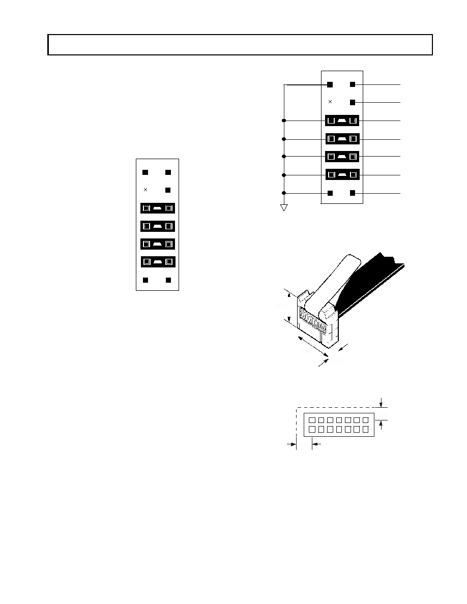
27
REV. 0
ADSP-2192M
Target Board Header
The emulator interface to an Analog Devices JTAG DSP is a
14-pin header, as shown in
Figure 9
. The customer must supply
this header on the target board in order to communicate with the
emulator. The interface consists of a standard dual row 0.025"
square post header, set on 0.1"
0.1" spacing, with a minimum
post length of 0.235". Pin 3 is the key position used to prevent
the pod from being inserted backwards. This pin must be clipped
on the target board.
Also, the clearance (length, width, and height) around the header
must be considered. Leave a clearance of at least 0.15" and 0.10"
around the length and width of the header, and reserve a height
clearance to attach and detach the pod connector.
As can be seen in
Figure 9
, there are two sets of signals on the
header. There are the standard JTAG signals TMS, TCK, TDI,
TDO,
TRST, and EMU used for emulation purposes (via an
emulator). There are also secondary JTAG signals BTMS,
BTCK, BTDI, and
BTRST that are optionally used for board-
level (boundary scan) testing.
When the emulator is not connected to this header, place jumpers
across BTMS, BTCK,
BTRST, and BTDI as shown in
Figure 10
. This holds the JTAG signals in the correct state to
allow the DSP to run free. Remove all the jumpers when con-
necting the emulator to the JTAG header.
JTAG Emulator Pod Connector
Figure 11
details the dimensions of the JTAG pod connector at
the 14-pin target end.
Figure 12
displays the keep-out area for a
target board header. The keep-out area allows the pod connector
to properly seat onto the target board header. This board area
should contain no components (such as chips, resistors, capaci-
tors). The dimensions are referenced to the center of the 0.25"
square post pin.
Design-for-Emulation Circuit Information
For details on target board design issues including: single
processor connections, multiprocessor scan chains, signal buff-
ering, signal termination, and emulator pod logic, see the EE-68:
Analog Devices
JTAG Emulation Technical Reference on the Analog
Devices website (
www.analog.com
)--use site search on
"EE-68." This document is updated regularly to keep pace with
improvements to emulator support.
Figure 9. JTAG Target Board Connector for JTAG
Equipped Analog Devices DSP (Jumpers in Place)
TOP VIEW
13
14
11
12
9
10
7
8
5
6
3
4
1
2
EMU
GND
TMS
TCK
TRST
TDI
TDO
GND
KEY (NO PIN)
BTMS
BTCK
BTRST
BTDI
GND
Figure 10. JTAG Target Board Connector
with No Local Boundary Scan
Figure 11. JTAG Pod Connector Dimensions
Figure 12. JTAG Pod Connector Keep-Out Area
TOP VIEW
13
14
11
12
9
10
7
8
5
6
3
4
1
2
EMU
GND
TMS
TCK
TRST
TDI
TDO
GND
KEY (NO PIN)
BTMS
BTCK
BTRST
BTDI
GND
0.64"
0.88"
0.24"
0.10"
0.15"

ADSP-2192M
28
REV. 0
Additional Information
This data sheet provides a general overview of the ADSP-2192M
architecture and functionality. For detailed information on the
ADSP-219x Family core architecture and instruction set, refer
to the ADSP-219x/2191 DSP Hardware Reference.
PIN DESCRIPTIONS
ADSP-2192M pin definitions are listed in a series of tables
following this section. Inputs identified as synchronous (S) must
meet timing requirements with respect to CLKIN (or with
respect to TCK for TMS, TDI). Inputs identified as asynchro-
nous (A) can be asserted asynchronously to CLKIN (or to TCK
for
TRST).
The following symbols appear in the Type columns of these
tables: G = Ground, I = Input, O = Output, P = Power Supply,
and T = Three-State.
Table 27. Pin Configurations:
PCI/USB Bus Interface
Pin Name
LQFP
I/O
Description
AD0
57
I/O
Addr/Data Bus
AD1
56
I/O
Addr/Data Bus
AD2
55
I/O
Addr/Data Bus
AD3
54
I/O
Addr/Data Bus
AD4
53
I/O
Addr/Data Bus
AD5
48
I/O
Addr/Data Bus
AD6
47
I/O
Addr/Data Bus
AD7
46
I/O
Addr/Data Bus
AD8
44
I/O
Addr/Data Bus
AD9
43
I/O
Addr/Data Bus
AD10
42
I/O
Addr/Data Bus
AD11
37
I/O
Addr/Data Bus
AD12
36
I/O
Addr/Data Bus
AD13
35
I/O
Addr/Data Bus
AD14
34
I/O
Addr/Data Bus
AD15
33
I/O
Addr/Data Bus
AD16
15
I/O
Addr/Data Bus
AD17
14
I/O
Addr/Data Bus
AD18
13
I/O
Addr/Data Bus
AD19
12
I/O
Addr/Data Bus
AD20
11
I/O
Addr/Data Bus
AD21
8
I/O
Addr/Data Bus
AD22
7
I/O
Addr/Data Bus
AD23
6
I/O
Addr/Data Bus
AD24
3
I/O
Addr/Data Bus
AD25
2
I/O
Addr/Data Bus
AD26
143
I/O
Addr/Data Bus
AD27
142
I/O
Addr/Data Bus
AD28
141
I/O
Addr/Data Bus
AD29
138
I/O
Addr/Data Bus
AD30
137
I/O
Addr/Data Bus
AD31
136
I/O
Addr/Data Bus
CBE0
45
I/O
PCI Cmd/Byte
Enable
CBE1
32
I/O
PCI Cmd/Byte
Enable
CBE2
16
I/O
PCI Cmd/Byte
Enable
CBE3
4
I/O
PCI Cmd/Byte
Enable
CLK
130
I
PCI Clock
CLKRUN
26
O
Clock Run
DEVSEL
24
I/O
PCI Target Select
FRAME
17
I/O
PCI Frame Select
GNT
131
I
Grant
IDSEL
5
I
PCI Initiator Select
INTAB
128
O
PCI/ISA Interrupt
IRDY
22
I/O
PCI Initiator Ready
PAR
31
I/O
PCI Bus Parity
PCIGND
1, 10,
21, 30,
39, 52,
133
I
PCI Ground
PCIVDD
9, 18,
29, 38,
51,
132,
144
I
PCI VDD supply
PERR
27
I/O
PCI Parity Error/
USB (Inverting
Input)
PME
135
O
PCI Power
Management Event
REQ
134
O
Request
RST
129
I
PCI Reset
SERR
28
O
PCI System Error/
USB+ (Noninverting
Input)
STOP
25
I/O
PCI Target Stop
TRDY
23
I/O
PCI Target Ready
Table 28. Pin Configurations: Analog Pins
Pin Name
LQFP
I/O
Description
AGND
67
I
Analog Gnd.
AQGND
68
I
Ref. Analog Gnd.
CTRLAUX
61
I
X Supply
CTRLVDD
63
I
Control VDD
IVDD
62
I
Digital VDD
NC
66
O
No Connect
NC
69
I
No Connect
NC
70
I
No Connect
RVAUX
60
I
X Supply
RVDD
64
I
Analog VDD Supply
Table 27. Pin Configurations:
PCI/USB Bus Interface (continued)
Pin Name
LQFP
I/O
Description

29
REV. 0
ADSP-2192M
Table 29. Pin Configurations: Emulator Pins
Pin Name
LQFP
I/O
Description
EMU
74
O
Emulator Event Pin
TCK
78
I
Emulator Clock
Input
TDI
80
I
Emulator Data Input
TDO
81
O
Emulator Data
Output
TMS
75
I
Emulator Mode
Select
TRST
79
I
Emulator Logic Reset
Table 30. Pin Configurations: Crystal/Configuration
Pins
Pin Name
LQFP
I/O
Description
BUS0
124
I
PCI/Sub-ISA/
CardBus Select Pins
BUS1
123
I
PCI/ Sub-ISA/
CardBus Select Pins
CLKSEL
116
I/O
Clock Select
IGND
122
I
IGND
NC
127
O
No Connect
PORST
121
I
Power-On Reset
XTALI
118
I
Crystal Input Pin
(24.576 MHz)
XTALO
119
I/O
Crystal Output Pin
Table 31. Pin Configurations: AC'97 Interface Pins
Pin Name
LQFP
I/O
Description
ACRST
102
O
AC'97 Reset
ACVAUX
92
I
AC'97 VAUX Input
ACVDD
93
I
AC'97 VDD Input
BITCLK
96
I
AC'97 Bit Clock
SDI0
99
I
AC'97 Serial Data
Input, Bit 0
SDI1
98
I
AC'97 Serial Data
Input, Bit 1
SDI2
97
I
AC'97 Serial Data
Input, Bit 2
SDO
100
O
AC'97 Serial Data
Output
SYNC
101
O
AC'97 Sync
Table 32. Pin Configurations: Serial EEPROM Pins
Pin Name
LQFP
I/O
Description
SCK
72
I
Serial EEPROM
Clock
SDA
71
I
Serial EEPROM Data
SEN
73
I
Serial EEPROM
Enable
Table 33. Pin Configurations: IO Pins
Pin Name
LQFP
I/O
Description
AIOGND
76, 91
IO Ground
IO0
82
I/O
IO Pin, Bit 0
IO1
83
I/O
IO Pin, Bit 1
IO2
84
I/O
IO Pin, Bit 2
IO3
86
I/O
IO Pin, Bit 3
IO4
87
I/O
IO Pin, Bit 4
IO5
88
I/O
IO Pin, Bit 5
IO6
89
I/O
IO Pin, Bit 6
IO7
90
I/O
IO Pin, Bit 7
IOVDD
77, 85
IO VDD
Table 34. Pin Configurations: Power Supply Pins
Pin Name
LQFP
I/O
Description
ACVAUX
92
AC'97
VAUX
Input
AIOGND
91
IO
Ground
AVDD
65
Analog VDD Supply
CTRLAUX
61
AUX
Control
CTRLVDD
63
Control
VDD
IGND
20, 41,
50, 59,
104,
120,
122,
126,
139
Digital
Ground
IVDD
19, 40,
49, 58,
62,
103,
117,
125,
140
Digital
VDD
RVAUX
60
AUX
Supply
RVDD
64
Analog VDD Supply

ADSP-2192M
30
REV. 0
SPECIFICATIONS
RECOMMENDED OPERATING CONDITIONS
K Grade Parameter
Test Conditions
Min
Max
Unit
V
DDINT
1
1
V
DDINT
= IVDD.
Internal Supply Voltage
2.38
2.62
V
V
DDEXT
2
2
V
DDEXT
= IOVDD, PCIVDD, ACVDD, RVDD, RVAUX, ACVAUX.
External Supply Voltage Option 3.3 V
(All Supplies)
3.0
3.6
V
V
DDEXT
3
3
V
DDEXT
= IOVDD, PCIVDD, ACVDD, RVDD only.
External Supply Voltage Option 5.0 V
(V
DDEXT
Supplies only)
4.75
5.25
V
V
IH1
High Level Input Voltage
4
4
Applies to PCI input and bidirectional pins.
@ V
DDEXT
= Max
2.0
V
DDEXT
V
V
IH2
High Level Input Voltage
5
5
Applies to I/O bus bidirectional pins.
@ V
DDEXT
= Max
0.65 V
DDEXT
V
DDEXT
V
V
IL1
Low Level Input Voltage
2
@
V
DDEXT
= Min
0.3
0.8
V
V
IL2
Low Level Input Voltage
6
6
Applies to input pins XTALI, BUS0, BUS1.
@ V
DDINT
= Min
0.3
0.4
V
T
AMB
Ambient Operating Temperature
0
70
°C
Specifications subject to change without notice.
ELECTRICAL CHARACTERISTICS
Parameter
Test Conditions
Min
Typ
Max
Unit
V
OH
High Level Output Voltage
1
1
Applies to output and bidirectional pins.
@ V
DDEXT
= min, I
OH
= 0.5 mA
2.4
V
V
OL
Low Level Output Voltage
1
@ V
DDEXT
= max, I
OL
= 2.0 mA
0.4
V
I
IH
High Level Input Current
2, 3
2
Applies to input.
3
Applies to input pins with internal pull-ups: EMS, EDI, ERSTB, SDA, SEN, SCR, BUS0, BUS1.
@ V
DDEXT
= max, V
IN
= V
DD
max
10
µA
I
IL
Low Level Input Current
2
@ V
DDEXT
= max, V
IN
= 0 V
10
µA
I
ILP
Low Level Input Current
3
@ V
DDEXT
= max, V
IN
= 0 V
250
µA
I
OZH
Three-State Leakage Current
4, 5
4
Applies to three-statable pins.
5
Applies to three-statable pins with internal pull-ups.
@ V
DDEXT
= max, V
IN
= V
DD
max
10
µA
I
OZL
Three-State Leakage Current
4
@ V
DDEXT
= max, V
IN
= 0 V
10
µA
I
DD
Supply Current Dynamic
(Internal)
6
6
DSP typical operating condition for supply current specification. DSP MACs, ALUs, and shifts 50%; data read/write/moves 30%, idle 20%.
@ 160 MHz V
DDINT
= 2.5 V
340
mA
I
DD-IDLE
Supply Current (Idle)
V
DDINT
= 2.5 V
45
mA
C
IN
Input Capacitance
7, 8
7
Applies to all signal pins.
8
Guaranteed, but not tested.
f
IN
=1 MHz, T
AMB
= 25°C,
V
DDINT
= 2.5 V
20
pF
I
DD
Power-Down
Supply Current (Power-Down)
T
AMB
= 25°C, V
DDINT
= 2.5 V
0.8
mA
Specifications subject to change without notice.
31
REV. 0
ADSP-2192M
ABSOLUTE MAXIMUM RATINGS
ESD SENSITIVITY
TIMING SPECIFICATIONS
This section contains timing information for the DSP's
external signals.
Programmable Flags Cycle Timing
Table 35
and
Figure 13
describe Programmable Flag operations.
The signals indicated are asynchronous and are not tied to any
clock.
Power Supply, Internal (V
DDINT
)
1
. . . . . . . . 0.3 V to +6.0 V
1
Stresses greater than those listed above may cause permanent damage to the
device. These are stress ratings only; functional operation of the device at these
or any other conditions greater than those indicated in the operational sections
of this specification is not implied. Exposure to absolute maximum rating
conditions for extended periods may affect device reliability.
Power Supply, External (V
DDEXT
) . . . . . . . 0.3 V to +6.0 V
Input Voltage (Signal Pins) . . . . . . 0.3 V to V
DDEXT
+ 0.3 V
T
STORE
Storage Temperature Range . . . . . . 65ºC to +150ºC
T
LEAD
Lead Temperature (5 seconds) max . . . . . . . . . 185ºC
CAUTION
ESD (electrostatic discharge) sensitive device. Electrostatic charges as high as 4000 V
readily accumulate on the human body and test equipment and can discharge without
detection. Although the ADSP-2192M features proprietary ESD protection circuitry,
permanent damage may occur on devices subjected to high energy electrostatic
discharges. Therefore, proper ESD precautions are recommended to avoid perfor-
mance degradation or loss of functionality.
Table 35. Programmable Flags Cycle Timing
Parameter
Min
Max
Unit
t
GPTW
GPIO Timing Pulsewidth
40
ns
t
XTALIHI
XTALI High Pulsewidth
10
ns
t
XTALILO
XTALI Low Pulsewidth
15
ns
t
ENABLE
I/O Pins
0
ns
t
DISABLE
I/O Pins
10
ns
Figure 13. Programmable Flags Cycle Timing
FLAG I/O PINS
CLK
t
DISABLE
t
ENABLE
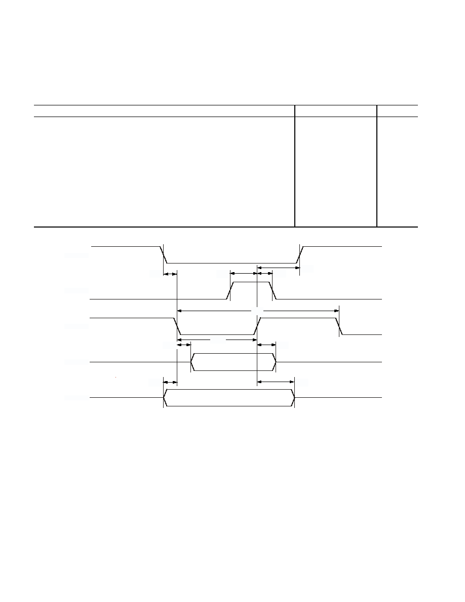
ADSP-2192M
32
REV. 0
Sub-ISA Interface Read/Write Cycle Timing
Table 36
,
Figure 14
, and
Figure 15
describe Sub-ISA Interface
Read and Write operations.
Table 36. Sub-ISA Interface Read/Write Cycle Timing
Parameter
Min
Max
Unit
t
ISTW
IOR/IOW Strobe Width
100
ns
t
ICYC
IOR/IOW Cycle Time
240
ns
t
AESU
AEN Setup to IOR/IOW Falling
10
ns
t
AEHD
AEN Hold from IOR/IOW Rising
0
ns
t
ADSU
Address Setup to
IOR/IOW Falling
10
ns
t
ADHD
Address Hold from
IOR/IOW Rising
0
ns
t
DHD1
Data Hold from
IOR Rising
20
ns
t
DHD2
Data Hold from
IOW Rising
15
ns
t
RDDV
IOR Falling to Valid Read Data
40
ns
t
WDSU
Write Data Setup to
IOW Rising
10
ns
t
RDY1
IOR/IOW Rising from IOCHRDY Rising
0
ns
t
RDY2
IOCHRDY Falling from
IOR/IOW Rising
20
ns
Figure 14. Sub-ISA Interface Read Cycle Timing
t
AESU
IOCHRDY
ISAD150
IOR
AEN
ISAA31
t
RDY1
t
RDY2
t
AEHD
t
ICYC
t
RDDV
t
DHD1
t
ISTW
t
ADSU
t
ADHD
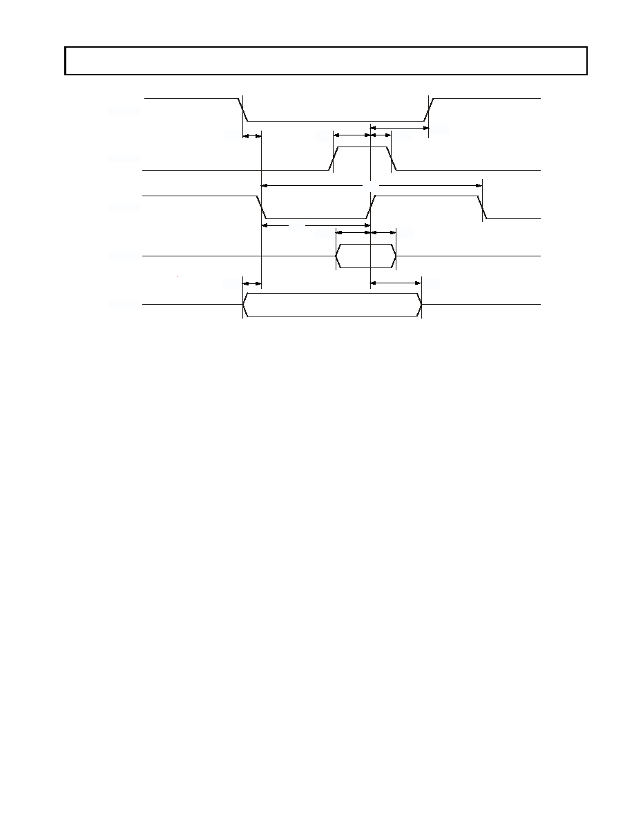
33
REV. 0
ADSP-2192M
Figure 15. Sub-ISA Interface Write Cycle Timing
t
AESU
IOCHRDY
ISAD150
IOW
AEN
ISAA31
t
RDY1
t
RDY2
t
AEHD
t
ICYC
t
WDSU
t
DHD2
t
STW
t
ADSU
t
ADHD
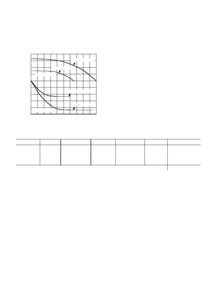
ADSP-2192M
34
REV. 0
Output Drive Currents
Figure 16
shows typical I-V characteristics for the output drivers
of the ADSP-2192M. The curves represent the current drive
capability of the output drivers as a function of output voltage.
Power Dissipation
Total power dissipation has two components, one due to internal
circuitry and one due to the switching of external output drivers.
Internal power dissipation is dependent on the instruction
execution sequence and the data operands involved.
The external component of total power dissipation is caused by
the switching of output pins. Its magnitude depends on:
·
Number of output pins that switch during each cycle (O)
·
The maximum frequency at which they can switch (f)
·
Their load capacitance (C)
·
Their voltage swing (V
DD
)
and is calculated by the formula below.
The load capacitance includes the processor's package capaci-
tance (C
IN
). The switching frequency includes driving the load
high and then back low. Address and data pins can drive high and
low at a maximum rate of 33 MHz.
The P
EXT
equation is calculated for each class of pins that can
drive as shown in
Table 37
.
A typical power consumption can now be calculated for these
conditions by adding a typical internal power dissipation with the
following formula.
Where:
·
P
EXT
is from
Table 37
·
P
INT
is I
DDINT
2.5 V, using the calculation I
DDINT
listed
in
Electrical Characteristics on Page 30
.
Note that the conditions causing a worst-case P
EXT
are different
from those causing a worst-case P
INT
. Maximum P
INT
cannot
occur while 100% of the output pins are switching from all ones
to all zeros. Note also that it is not common for an application to
have 100% or even 50% of the outputs switching simultaneously.
Test Conditions
The ADSP-2192M is tested for compliance with all support
industry standard interfaces (PCI, USB, and AC'97). Also, the
DSP is tested for output enable, disable, and pulsewidth. See
Table 35
for the values of these parameters.
Output Disable Time
Output pins are considered to be disabled when they stop driving,
go into a high impedance state, and start to decay from their
output high or low voltage. The time for the voltage on the bus
to decay by
V is dependent on the capacitive load, C
L
and the
load current, I
L
. This decay time can be approximated by the
equation below.
The output disable time t
DIS
is the difference between t
MEASURED
and t
DECAY
as shown in
Figure 17
. The time t
MEASURED
is the
interval from when the reference signal switches to when the
output voltage decays
V from the measured output high or
output low voltage. The t
DECAY
is calculated with test loads C
L
and
I
L
, and with
V equal to 0.5 V.
Output Enable Time
Output pins are considered to be enabled when they have made
a transition from a high impedance state to when they start
driving. The output enable time t
ENA
is the interval from when a
reference signal reaches a high or low voltage level to when the
Figure 16. Typical Drive Currents
SOURCE (V
DDEXT
) VOLTAGE V
0
3.5
0.5
1.0
1.5
2.0
2.5
3.0
4.0
S
O
U
R
C
E
(
V
D
D
E
X
T
)
C
U
R
R
E
N
T
m
A
100
80
60
40
20
0
20
40
60
V
DDEXT
= 3.3V @
25°C
V
DD EXT
= 5.0V @
25°C
V
OH
V
OL
INPUT CURRENT
OUTPUT CURRENT
80
4.5
5.0
V
DDEXT
= 3.3V @
25°C
V
DD EX T
= 5.0V @
25°C
P
EXT
O
C
×
V
DD
2
×
f
×
=
Table 37. P
EXT
Calculation Example
Pin Type
No. of Pins % Switching
C
f
V
DD
2
= P
EXT
Address/Data 32
100
10 pF
33 MHz
10.9 V
= 0.115 W
DEVSEL
1
0
10 pF
33 MHz
10.9 V
= 0.0 W
CBE
1
100
10 pF
33 MHz
10.9 V
= 0.003 W
CLK
1
100
10 pF
33 MHz
10.9 V
= 0.003 W
P
EXT
= 0.04687 W
P
TOTAL
P
=
EXT
P
INT
+
t
DECAY
C
L
V
I
L
---------------
=
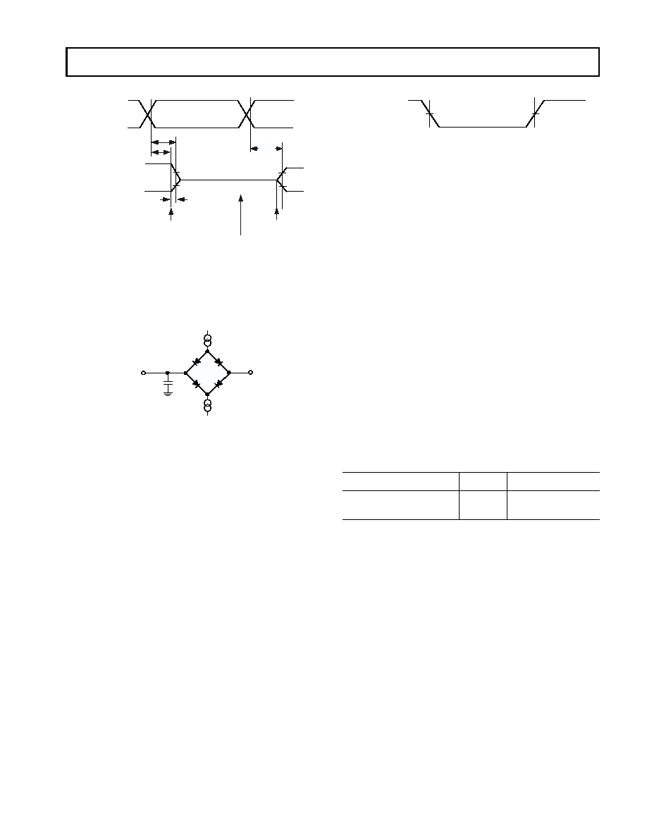
35
REV. 0
ADSP-2192M
output has reached a specified high or low trip point, as shown
in the Output Enable/Disable diagram (
Figure 17
). If multiple
pins (such as the data bus) are enabled, the measurement value
is that of the first pin to start driving.
Example System Hold Time Calculation
To determine the data output hold time in a particular system,
first calculate t
DECAY
using the equation at
Output Disable Time
on Page 34
. Choose
V to be the difference between the ADSP-
2192M's output voltage and the input threshold for the device
requiring the hold time. A typical
V will be 0.4 V. C
L
is the total
bus capacitance (per data line), and I
L
is the total leakage or three-
state current (per data line). The hold time will be t
DECAY
plus the
minimum disable time (i.e., t
DATRWH
for the write cycle).
Capacitive Loading
Output delays and holds are based on standard capacitive loads:
50 pF on all pins. The delay and hold specifications given should
be derated for loads other than the nominal value of 50 pF.
Environmental Conditions
The thermal characteristics in which the DSP is operating
influence performance (see
Table 38
).
Figure 17. Output Enable/Disable
Figure 18. Equivalent Device Loading for AC
Measurements (Includes All Fixtures)
REFERENCE
SIGNAL
t
DIS
OUTPUT STARTS
DRIVING
V
OH (MEASURED)
V 2.0V
V
OL (MEASURED)
+
V 1.0V
t
MEASURED
V
OH (MEASURED)
V
OL (MEASURED)
HIGH IMPEDANCE STATE.
TEST CONDITIONS CAUSE THIS VOLTAGE
TO BE APPROXIMATELY 1.5V
OUTPUT STOPS
DRIVING
t
DECAY
t
ENA
1.5V
50pF
TO
OUTPUT
PIN
I
OL
I
OH
Figure 19. Voltage Reference Levels for AC
Measurements (Except Output Enable/Disable)
Table 38. Thermal Characteristics
Rating Description
Symbol
LQFP
Thermal Resistance
(Junction-to-Ambient)
JA
33.79°C/W
Still Air
INPUT
OR
O UTPUT
1.5V
1.5V

ADSP-2192M
36
REV. 0
144-Lead LQFP Pinout
Table 39
lists the LQFP pinout by signal name.
Table 40
lists
the LQFP pinout by pin number.
Table 39. 144-Lead LQFP Pins (Alphabetically by Signal)
Signal
Pin
No.
Signal
Pin
No.
Signal
Pin
No.
Signal
Pin
No.
Signal
Pin
No.
ACRST
102
AD26
143
IDSEL
5
IVDD
125
PCIVDD
51
ACVAUX
92
AD27
142
IGND
20
IVDD
140
PCIVDD
132
ACVDD
93
AD28
141
IGND
41
IVDD
62
PCIVDD
144
AD0
57
AD29
138
IGND
50
NC
115
PERR
27
AD1
56
AD30
137
IGND
59
NC
114
PME
135
AD2
55
AD31
136
IGND
104
NC
108
PORST
121
AD3
54
AGND
67
IGND
120
NC
105
REQ
134
AD4
53
AIOGND
91
IGND
122
NC
109
RST
129
AD5
48
AQGND
68
IGND
126
NC
107
RVAUX
60
AD6
47
AVDD
65
IGND
139
NC
106
RVDD
64
AD7
46
ACVAUX
113
INTAB
128
NC
110
SCK
72
AD8
44
ACVDD
112
IO0
82
NC
127
SDA
71
AD9
43
BITCLK
96
IO1
83
NC
70
SDI0
99
AD10
42
BUS0
124
IO2
84
NC
66
SDI1
98
AD11
37
BUS1
123
IO3
86
NC
94
SDI2
97
AD12
36
CBE0
45
IO4
87
NC
69
SDO
100
AD13
35
CBE1
32
IO5
88
NC
95
SEN
73
AD14
34
CBE2
16
IO6
89
PAR
31
SERR
28
AD15
33
CBE3
4
IO7
90
PCIGND
1
STOP
25
AD16
15
CLK
130
IOGND
76
PCIGND
10
SYNC
101
AD17
14
CLKRUN
26
IOVDD
77
PCIGND
21
TCK
78
AD18
13
CLKSEL
116
IOVDD
85
PCIGND
30
TDI
80
AD19
12
CTRLAUX
61
IRDY
22
PCIGND
39
TDO
81
AD20
11
CTRLVDD
63
IVDD
19
PCIGND
52
TMS
75
AD21
8
DEVSEL
24
IVDD
40
PCIGND
133
TRDY
23
AD22
7
EMU
74
IVDD
49
PCIVDD
9
TRST
79
AD23
6
FRAME
17
IVDD
58
PCIVDD
18
XTALI
118
AD24
3
GND
111
IVDD
103
PCIVDD
29
XTALO
119
AD25
2
GNT
131
IVDD
117
PCIVDD
38

37
REV. 0
ADSP-2192M
Table 40. 144-Lead LQFP Pins (Numerically by Pin Number)
Pin
No.
Signal
Pin
No.
Signal
Pin
No.
Signal
Pin
No.
Signal
Pin
No.
Signal
1
PCIGND
30
PCIGND
59
IGND
88
IO5
117
IVDD
2
AD25
31
PAR
60
RVAUX
89
IO6
118
XTALI
3
AD24
32
CBE1
61
CTRLAUX
90
IO7
119
XTALO
4
CBE3
33
AD15
62
IVDD
91
AIOGND
120
IGND
5
IDSEL
34
AD14
63
CTRLVDD
92
ACVAUX
121
PORST
6
AD23
35
AD13
64
RVDD
93
ACVDD
122
IGND
7
AD22
36
AD12
65
AVDD
94
NC
123
BUS1
8
AD21
37
AD11
66
NC
95
NC
124
BUS0
9
PCIVDD
38
PCIVDD
67
AGND
96
BITCLK
125
IVDD
10
PCIGND
39
PCIGND
68
AQGND
97
SDI2
126
IGND
11
AD20
40
IVDD
69
NC
98
SDI1
127
NC
12
AD19
41
IGND
70
NC
99
SDI0
128
INTAB
13
AD18
42
AD10
71
SDA
100
SDO
129
RST
14
AD17
43
AD9
72
SCK
101
SYNC
130
CLK
15
AD16
44
AD8
73
SEN
102
ACRST
131
GNT
16
CBE2
45
CBE0
74
EMU
103
IVDD
132
PCIVDD
17
FRAME
46
AD7
75
TMS
104
IGND
133
PCIGND
18
PCIVDD
47
AD6
76
IOGND
105
NC
134
REQ
19
IVDD
48
AD5
77
IOVDD
106
NC
135
PME
20
IGND
49
IVDD
78
TCK
107
NC
136
AD31
21
PCIGND
50
IGND
79
TRST
108
NC
137
AD30
22
IRDY
51
PCIVDD
80
TDI
109
NC
138
AD29
23
TRDY
52
PCIGND
81
TDO
110
NC
139
IGND
24
DEVSEL
53
AD4
82
IO0
111
GND
140
IVDD
25
STOP
54
AD3
83
IO1
112
ACVDD
141
AD28
26
CLKRUN
55
AD2
84
IO2
113
ACVAUX
142
AD27
27
PERR
56
AD1
85
IOVDD
114
NC
143
AD26
28
SERR
57
AD0
86
IO3
115
NC
144
PCIVDD
29
PCIVDD
58
IVDD
87
IO4
116
CLKSEL
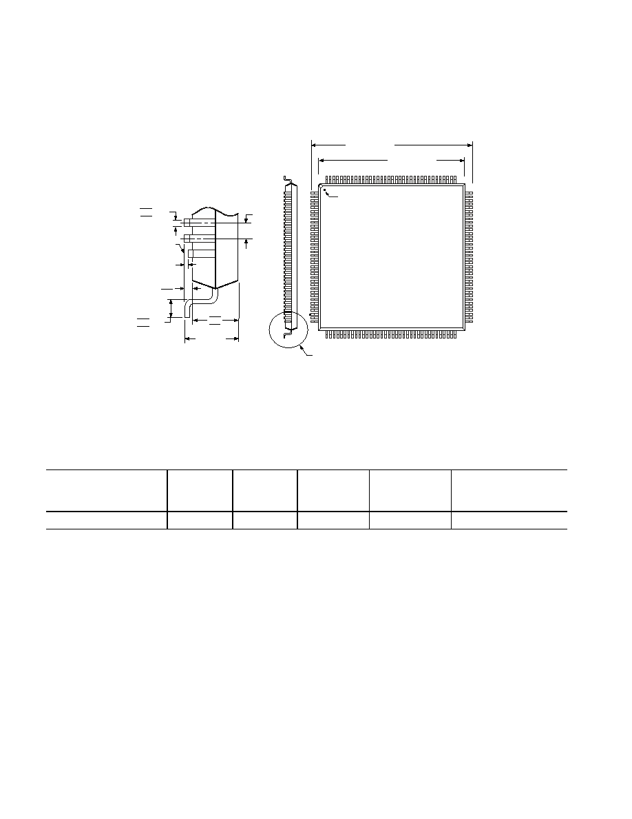
ADSP-2192M
38
REV. 0
OUTLINE DIMENSIONS
ORDERING GUIDE
144-Lead Plastic Quad Flatpack [LQFP]
(ST-144)
Part Number
1
1
ST = Plastic Quad Flatpack (LQFP).
Ambient
Temperature
Range
Instruction
Rate
On-Chip
SRAM
Package
Description
Operating Voltage
ADSP-219212MKST160
0ºC to 70ºC
160 MHz
2.4 Mbit
144-Lead LQFP
2.5 Int./3.3 or 5 Ext. V
SEATING
PLANE
1.60 MAX
0.15
0.05
0.08 MAX (LEAD
COPLANARITY)
1.45
1.40
1.35
0.27
0.22
0.17
TYP
0.50
BSC
TYP
(LEAD
PITCH)
1
3 6
37
73
72
108
144
109
TOP VIEW (PINS DOWN)
22.00 BSC SQ
20.00 BSC SQ
DIMENSIONS ARE IN MILLIMETERS AND COMPLY WITH JEDEC STANDARD MS-026-BFB.
ACTUAL POSITION OF EACH LEAD IS WITHIN 0.08 OF ITS
IDEAL POSITION, WHEN MEASURED IN THE LATERAL DIRECTION.
CENTER DIMENSIONS ARE NOMINAL.
NOTES:
3.
2.
1.
DETAIL A
DETAIL A
PIN 1 INDICATOR
0.75
0.60 TYP
0.45

39

40
PRINTED IN
U.S.A.
C0
25
66
0
1
1
/
0
2
(
0)
Document Outline