 | ÐлекÑÑоннÑй компоненÑ: ADSP-2195 | СкаÑаÑÑ:  PDF PDF  ZIP ZIP |
Äîêóìåíòàöèÿ è îïèñàíèÿ www.docs.chipfind.ru
a
Preliminary Technical Data
DSP Microcomputer
This information applies to a product under development. Its characteristics
and specifications are subject to change without notice. Analog Devices
assumes no obligation regarding future manufacturing unless otherwise
agreed to in writing.
One Technology Way, P.O.Box 9106, Norwood, MA 02062-9106, U.S.A.
Tel:781/329-4700
World Wide Web Site: http://www.analog.com
Fax:781/326-8703
©Analog Devices,Inc., 2001
REV. PrA
35(/,0,1$5< 7(&+1,&$/ '$7$
ADSP-2195
ADSP-219x DSP CORE FEATURES
6.25 ns Instruction Cycle Time (Internal), for up to
160 MIPS Sustained Performance
ADSP-218x Family Code Compatible with the Same
Easy -to-Use Algebraic Syntax
Single-Cycle Instruction Execution
Up to 16M words of Addressable Memory Space with
24 Bits of Addressing Width
Dual Purpose Program Memory for Both Instruction and
Data Storage
Fully Transparent Instruction Cache Allows Dual
Operand Fetches in Every Instruction Cycle
Unified Memory Space Permits Flexible Address
Generation, Using Two Independent DAG Units
Independent ALU, Multiplier/Accumulator, and Barrel
Shifter Computational Units with Dual 40-bit
Accumulators
Single-Cycle Context Switch between Two Sets of
Computational and DAG Registers
Parallel Execution of Computation and Memory
Instructions
Pipelined Architecture Supports Efficient Code
Execution at Speeds up to 160 MIPS
Register File Computations with All Nonconditional,
Nonparallel Computational Instructions
Powerful Program Sequencer Provides Zero-Overhead
Looping and Conditional Instruction Execution
Architectural Enhancements for Compiled C
Code Efficiency
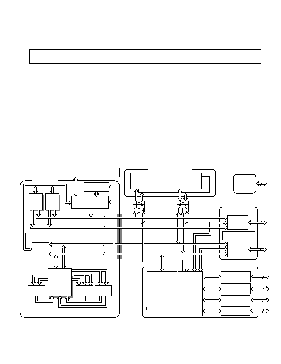
FUNCTIONAL BLOCK DIAGRAM
6 ( 5 , $ / 3 2 5 7 6
6 3 , 3 2 5 7 6
, 2 5 ( * , 6 7 ( 5 6
0 ( 0 2 5 < 0 $ 3 3 ( '
& 2 1 7 5 2 /
6 7 $ 7 8 6
% 8 ) ) ( 5 6
,2 3 5 2 & ( 6 6 2 5
, 1 7 ( 5 5 8 3 7 & 2 1 7 5 2 / / ( 5
7 , 0 ( 5 6 ) / $ * 6
& $ & + (
×
×
×
×
% , 7
- 7 $ *
7 ( 6 7
( 0 8 / $ 7 , 2 1
$ ' ' 5 % 8 6
0 8 ;
( ; 7 ( 5 1 $ / 0 ( 0 2 5 <
, 1 7 ( 5 ) $ & (
( ; 7 ( 5 1 $ /
3 2 5 7
' $ 7 $ % 8 6
0 8 ;
3 0 $ ' ' 5 ( 6 6 % 8 6
' 0 $ ' ' 5 ( 6 6 % 8 6
3 0 ' $ 7 $ % 8 6
' 0 ' $ 7 $ % 8 6
% 8 6
& 2 1 1 ( & 7
3 ;
$ ' 6 3 [
' 6 3 & 2 5 (
3 5 2 * 5 $ 0
6 ( 4 8 ( 1 & ( 5
' $ 7 $
5 ( * , 6 7 ( 5
) , / (
0 8 / 7
% $ 5 5 ( /
6 + , ) 7 ( 5
$ / 8
8 $ 5 7 3 2 5 7
' 0 $
& 2 1 7 5 2 / / ( 5
, 1 3 8 7
5 ( * , 6 7 ( 5 6
5 ( 6 8 / 7
5 ( * , 6 7 ( 5 6
×
×
×
×
% , 7
+ 2 6 7 3 2 5 7
' $ *
×
×
×
×
×
×
×
×
' $ *
×
×
×
×
×
×
×
×
' $ 7 $
' $ 7 $
$ ' ' 5 ( 6 6
7 : 2 , 1 ' ( 3 ( 1 ' ( 1 7 % / 2 & . 6
,1 7 ( 5 1 $ / 0 ( 0 2 5 <
$ ' ' 5 ( 6 6
' 0 $
' $ 7 $
' 0 $
$ ' ' 5 ( 6 6
%
/
2
&
.
%
/
2
&
.

For current information contact Analog Devices at 800/262-5643
ADSP-2195
September 2001
This information applies to a product under development. Its characteristics and specifications are subject to change with-
out notice. Analog Devices assumes no obligation regarding future manufacturing unless otherwise agreed to in writing.
2
REV. PrA
35(/,0,1$5< 7(&+1,&$/ '$7$
ADSP-2195 DSP FEATURES
32K Words of On-Chip RAM, Configured as 16K Words
On-Chip 24-bit RAM and 16K Words On-Chip
16-bit RAM
16K Words of On-Chip 24-bit ROM
Architecture Enhancements beyond ADSP-218x Family
are Supported with Instruction Set Extensions for
Added Registers, Ports, and Peripherals
Flexible Power Management with Selectable
Power-Down and Idle Modes
Programmable PLL Supports 1 to 32 Frequency
Multiplication, Enabling Full-Speed Operation from
Low-Speed Input Clocks
2.5 V Internal Operation Supports 3.3 V Compliant I/O
Three Full-Duplex Multichannel Serial Ports, Each
Supporting H.100 Standard with A-Law and -Law
Companding in Hardware
Two SPI-Compatible Ports with DMA Capability
One UART Port with DMA Capability
16 General-Purpose I/O Pins (Eight Dedicated/Eight
Programmable from the External Memory Interface)
with Integrated Interrupt Support
Three Programmable 32-Bit Interval Timers with
Pulsewidth Counter, PWM Generation, and Externally
Clocked Timer Capabilities
Up to 11 DMA Channels can be Active at any Given Time
Host Port With DMA Capability for Efficient, Glueless Host
Interface (16-Bit Transfers)
External Memory Interface Features Include:
Direct Access from the DSP to External Memory for
Data and Instructions.
Support for DMA Block Transfers to/from
External Memory.
Separate Peripheral Memory Space with Parallel
Support for 224K External 16-Bit Registers.
Four General-Purpose Memory Select Signals that
Provide Access to Separate Banks of External
Memory. Bank Boundaries and Size Are User-
Programmable.
Programmable Waitstate Logic with ACK Signal and
Separate Read and Write Wait Counts. Wait Mode
Completion Supports All Combinations of ACK
and/or Wait Count.
I/O Clock Rate Can Be Set to the Peripheral Clock Rate
Divided by 1, 2, 4, 16, or 32 to Allow Interface to Slow
Memory Devices.
Address Translation and Data Word Packing is Provided
to Support an 8- or 16-Bit External Data Bus.
Programmable Read and Write Strobe Polarity.
Separate Configuration Registers for the Four
General-Purpose, Peripheral, and Boot
Memory Spaces.
Bus Request and Grant Signals Support the Use of the
External Bus by an External Device.
Boot Methods Include Booting Through External Memory
Interface, SPI Ports, UART Port, or Host Interface
IEEE JTAG Standard 1149.1 Test Access Port Supports
On-Chip Emulation and System Debugging
144-Lead LQFP Package (20
20
1.4 mm) and 144-Lead
Mini-BGA Package (10
10
1.25 mm)

This information applies to a product under development. Its characteristics and specifications are subject to change with-
out notice. Analog Devices assumes no obligation regarding future manufacturing unless otherwise agreed to in writing.
3
REV. PrA
For current information contact Analog Devices at 800/262-5643
ADSP-2195
September 2001
35(/,0,1$5< 7(&+1,&$/ '$7$
TABLE OF CONTENTS
ADSP-219x dSP Core Features . . . . . . . . . . . . . . . . . 1
Functional Block Diagram. . . . . . . . . . . . . . . . . . . . . . 2
General Description . . . . . . . . . . . . . . . . . . . . . . . . . . 4
DSP Core Architecture . . . . . . . . . . . . . . . . . . . . . . . 4
DSP Peripherals Architecture . . . . . . . . . . . . . . . . . . . 5
Memory Architecture . . . . . . . . . . . . . . . . . . . . . . . . . 6
Internal (On-Chip) Memory . . . . . . . . . . . . . . . . 6
Internal On-Chip ROM . . . . . . . . . . . . . . . . . . . . 6
On-Chip Memory Security . . . . . . . . . . . . . . . . . 7
External (Off-Chip) Memory . . . . . . . . . . . . . . . . 8
External Memory Space . . . . . . . . . . . . . . . . . . . . 8
I/O Memory Space . . . . . . . . . . . . . . . . . . . . . . . 8
Boot Memory Space . . . . . . . . . . . . . . . . . . . . . . 8
Interrupts . . . . . . . . . . . . . . . . . . . . . . . . . . . . . . . . . . 8
DMA Controller . . . . . . . . . . . . . . . . . . . . . . . . . . . . 9
Host Port . . . . . . . . . . . . . . . . . . . . . . . . . . . . . . . . . 10
Host Port Acknowledge (HACK) Modes . . . . . . 10
Host Port Chip Selects . . . . . . . . . . . . . . . . . . . 11
DSP Serial Ports (SPORTs) . . . . . . . . . . . . . . . . . . . 11
Serial Peripheral Interface (SPI) Ports . . . . . . . . . . . 11
UART Port . . . . . . . . . . . . . . . . . . . . . . . . . . . . . . . 12
Programmable Flag (PFx) Pins . . . . . . . . . . . . . . . . . 12
Low Power Operation . . . . . . . . . . . . . . . . . . . . . . . 13
Idle Mode . . . . . . . . . . . . . . . . . . . . . . . . . . . . . 13
Power-down Core Mode . . . . . . . . . . . . . . . . . . 13
Power-Down Core/Peripherals Mode . . . . . . . . . 13
Power-Down All Mode . . . . . . . . . . . . . . . . . . . 13
Clock Signals . . . . . . . . . . . . . . . . . . . . . . . . . . . . . . 14
Reset . . . . . . . . . . . . . . . . . . . . . . . . . . . . . . . . . . . . 14
Power Supplies . . . . . . . . . . . . . . . . . . . . . . . . . . . . . 14
Booting Modes . . . . . . . . . . . . . . . . . . . . . . . . . . . . . 15
Bus Request and Bus Grant . . . . . . . . . . . . . . . . . . . 16
Instruction Set Description . . . . . . . . . . . . . . . . . . . . 16
Development Tools . . . . . . . . . . . . . . . . . . . . . . . . . 16
Designing an Emulator-Compatible DSP Board
(Target) . . . . . . . . . . . . . . . . . . . . . . . . . . . 17
Target Board Header . . . . . . . . . . . . . . . . . . . . . 17
JTAG Emulator Pod Connector . . . . . . . . . . . . 18
Design-for-Emulation Circuit Information . . . . . 18
Additional Information . . . . . . . . . . . . . . . . . . . . . . . 18
Pin Descriptions . . . . . . . . . . . . . . . . . . . . . . . . . . . . 18
Specifications . . . . . . . . . . . . . . . . . . . . . . . . . . . . . . 22
Recommended Operating Conditions . . . . . . . . . . 22
Electrical Characteristics . . . . . . . . . . . . . . . . . . . . 22
ABSOLUTE MAXIMUM RATINGS . . . . . . . . . . 24
ESD SENSITIVITY . . . . . . . . . . . . . . . . . . . . . . . . 24
Timing Specifications . . . . . . . . . . . . . . . . . . . . . . . 24
Clock In and Clock Out Cycle Timing . . . . . . . 25
Programmable Flags Cycle Timing . . . . . . . . . . 26
Timer PWM_OUT Cycle Timing . . . . . . . . . . . 27
External Port Write Cycle Timing . . . . . . . . . . . 28
External Port Read Cycle Timing . . . . . . . . . . . 30
External Port Bus Request and Grant Cycle
Timing . . . . . . . . . . . . . . . . . . . . . . . . . . . . 32
Host Port ALE Mode Write Cycle Timing . . . . 34
Host Port ACC Mode Write Cycle Timing . . . . 36
Host Port ALE Mode Read Cycle Timing . . . . . 38
Host Port ACC Mode Read Cycle Timing . . . . 40
Serial Port (SPORT) Clocks and Data Timing . 42
Serial Port (SPORT) Frame Synch Timing . . . . 44
Serial Peripheral Interface (SPI) Port--Master
Timing . . . . . . . . . . . . . . . . . . . . . . . . . . . . 46
Serial Peripheral Interface (SPI) Port--Slave
Timing . . . . . . . . . . . . . . . . . . . . . . . . . . . . 48
Universal Asynchronous Receiver-Transmitter
(UART) Port--Receive and Transmit
Timing . . . . . . . . . . . . . . . . . . . . . . . . . . . . 50
JTAG Test And Emulation Port Timing . . . . . . 51
Output Drive Currents . . . . . . . . . . . . . . . . . . . . . . 52
Power Dissipation . . . . . . . . . . . . . . . . . . . . . . . . . . 52
Test Conditions . . . . . . . . . . . . . . . . . . . . . . . . . . . . 54
Output Disable Time . . . . . . . . . . . . . . . . . . . . 54
Output Enable Time . . . . . . . . . . . . . . . . . . . . . 54
Example System Hold Time Calculation . . . . . . 55
Capacitive Loading . . . . . . . . . . . . . . . . . . . . . . 55
Environmental Conditions . . . . . . . . . . . . . . . . . . . . 55
Thermal Characteristics . . . . . . . . . . . . . . . . . . 55
ADSP-2195 144-Lead LQFP Pinout . . . . . . . . . . . . 58
ADSP-2195 144-Lead Mini-BGA Pinout . . . . . . . . 67
Ordering Guide . . . . . . . . . . . . . . . . . . . . . . . . . . . . 68

For current information contact Analog Devices at 800/262-5643
ADSP-2195
September 2001
This information applies to a product under development. Its characteristics and specifications are subject to change with-
out notice. Analog Devices assumes no obligation regarding future manufacturing unless otherwise agreed to in writing.
4
REV. PrA
35(/,0,1$5< 7(&+1,&$/ '$7$
General Note
This data sheet provides preliminary information for the
ADSP-2195 Digital Signal Processor.
GENERAL DESCRIPTION
The ADSP-2195 DSP is a single-chip microcomputer
optimized for digital signal processing (DSP) and other high
speed numeric processing applications.
The ADSP-2195 combines the ADSP-219x family base
architecture (three computational units, two data address
generators, and a program sequencer) with three serial
ports, two SPI-compatible ports, one UART port, a DMA
controller, three programmable timers, general-purpose
Programmable Flag pins, extensive interrupt capabilities,
and on-chip program and data memory spaces.
The ADSP-2195 architecture is code-compatible with
ADSP-218x family DSPs. Although the architectures are
compatible, the ADSP-2195 architecture has a number of
enhancements over the ADSP-218x architecture. The
enhancements to computational units, data address gener-
ators, and program sequencer make the ADSP-2195 more
flexible and even easier to program than the
ADSP-218x DSPs.
Indirect addressing options provide addressing flexibility--
premodify with no update, pre- and post-modify by an
immediate 8-bit, two's-complement value and base address
registers for easier implementation of circular buffering.
The ADSP-2195 integrates 48K words of on-chip memory
configured as 16K words (24-bit) of program RAM, 16K
words (16-bit) of data RAM, and 16K words (24-bit) of
program ROM. Power-down circuitry is also provided to
meet the low power needs of battery-operated portable
equipment. The ADSP-2195 is available in 144-lead LQFP
and mini-BGA packages.
Fabricated in a high-speed, low-power, CMOS process, the
ADSP-2195 operates with a 6.25 ns instruction cycle time
(160 MIPS). All instructions, except two multiword
instructions, can execute in a single DSP cycle.
The ADSP-2195's flexible architecture and comprehensive
instruction set support multiple operations in parallel. For
example, in one processor cycle, the ADSP-2195 can:
· Generate an address for the next instruction fetch
· Fetch the next instruction
· Perform one or two data moves
· Update one or two data address pointers
· Perform a computational operation
These operations take place while the processor
continues to:
· Receive and transmit data through two serial ports
· Receive and/or transmit data from a Host
· Receive or transmit data through the UART
· Receive or transmit data over two SPI ports
· Access external memory through the external memory
interface
· Decrement the timers
DSP Core Architecture
The ADSP-2195 instruction set provides flexible data
moves and multifunction (one or two data moves with a
computation) instructions. Every single-word instruction
can be executed in a single processor cycle. The ADSP-2195
assembly language uses an algebraic syntax for ease of
coding and readability. A comprehensive set of development
tools supports program development.
The functional block diagram
on page 1
shows the architec-
ture of the ADSP-219x core. It contains three independent
computational units: the ALU, the multiplier/accumulator
(MAC), and the shifter. The computational units process
16-bit data from the register file and have provisions to
support multiprecision computations. The ALU performs
a standard set of arithmetic and logic operations; division
primitives are also supported. The MAC performs sin-
gle-cycle multiply, multiply/add, and multiply/subtract
operations. The MAC has two 40-bit accumulators, which
help with overflow. The shifter performs logical and arith-
metic shifts, normalization, denormalization, and derive
exponent operations. The shifter can be used to efficiently
implement numeric format control, including multiword
and block floating-point representations.
Register-usage rules influence placement of input and
results within the computational units. For most operations,
the computational units' data registers act as a data register
file, permitting any input or result register to provide input
to any unit for a computation. For feedback operations, the
computational units let the output (result) of any unit be
input to any unit on the next cycle. For conditional or mul-
tifunction instructions, there are restrictions on which data
registers may provide inputs or receive results from each
computational unit. For more information, see the
ADSP-219x DSP Instruction Set Reference.
A powerful program sequencer controls the flow of instruc-
tion execution. The sequencer supports conditional jumps,
subroutine calls, and low interrupt overhead. With internal
loop counters and loop stacks, the ADSP-2195 executes
looped code with zero overhead; no explicit jump instruc-
tions are required to maintain loops.
Two data address generators (DAGs) provide addresses for
simultaneous dual operand fetches (from data memory and
program memory). Each DAG maintains and updates four
16-bit address pointers. Whenever the pointer is used to
access data (indirect addressing), it is pre- or post-modified
by the value of one of four possible modify registers. A length
value and base address may be associated with each pointer
to implement automatic modulo addressing for circular
buffers. Page registers in the DAGs allow circular addressing
This information applies to a product under development. Its characteristics and specifications are subject to change with-
out notice. Analog Devices assumes no obligation regarding future manufacturing unless otherwise agreed to in writing.
5
REV. PrA
For current information contact Analog Devices at 800/262-5643
ADSP-2195
September 2001
35(/,0,1$5< 7(&+1,&$/ '$7$
within 64K word boundaries of each of the 256 memory
pages, but these buffers may not cross page boundaries.
Secondary registers duplicate all the primary registers in the
DAGs; switching between primary and secondary registers
provides a fast context switch.
Efficient data transfer in the core is achieved with the use of
internal buses:
· Program Memory Address (PMA) Bus
· Program Memory Data (PMD) Bus
· Data Memory Address (DMA) Bus
· Data Memory Data (DMD) Bus
· DMA Address Bus
· DMA Data Bus
The two address buses (PMA and DMA) share a single
external address bus, allowing memory to be expanded
off-chip, and the two data buses (PMD and DMD) share a
single external data bus. Boot memory space and I/O
memory space also share the external buses.
Program memory can store both instructions and data, per-
mitting the ADSP-2195 to fetch two operands in a single
cycle, one from program memory and one from data
memory. The DSP's dual memory buses also let the
ADSP-219x core fetch an operand from data memory and
the next instruction from program memory in a single cycle.
DSP Peripherals Architecture
The functional block diagram
on page 1
shows the DSP's
on-chip peripherals, which include the external memory
interface, Host port, serial ports, SPI-compatible ports,
UART port, JTAG test and emulation port, timers, flags,
and interrupt controller. These on-chip peripherals can
connect to off-chip devices as shown in
Figure 1
.
The ADSP-2195 has a 16-bit Host port with DMA capa-
bility that lets external Hosts access on-chip memory. This
24-pin parallel port consists of a 16-pin multiplexed
data/address bus and provides a low-service overhead data
move capability. Configurable for 8- or 16-bits, this port
provides a glueless interface to a wide variety of 8- and 16-bit
microcontrollers. Two chip-selects provide Hosts access to
the DSP's entire memory map. The DSP is bootable
through this port.
The ADSP-2195 also has an external memory interface that
is shared by the DSP's core, the DMA controller, and DMA
capable peripherals, which include the UART, SPORT0,
SPORT1, SPORT2, SPI0, SPI1, and the Host port. The
external port consists of a 16-bit data bus, a 22-bit address
bus, and control signals. The data bus is configurable to
provide an 8 or 16 bit interface to external memory. Support
for word packing lets the DSP access 16- or 24-bit words
from external memory regardless of the external data bus
width. When configured for an 8-bit interface, the unused
eight lines provide eight programmable, bidirectional gen-
eral-purpose Programmable Flag lines, six of which can be
mapped to software condition signals.
The memory DMA controller lets the ADSP-2195 move
data and instructions from between memory spaces: inter-
nal-to-external, internal-to-internal, and external-to-
external. On-chip peripherals can also use this controller for
DMA transfers.
The ADSP-2195 can respond to up to seventeen interrupts
at any given time: three internal (stack, emulator kernel, and
power-down), two external (emulator and reset), and twelve
user-defined (peripherals) interrupts. Programmers assign
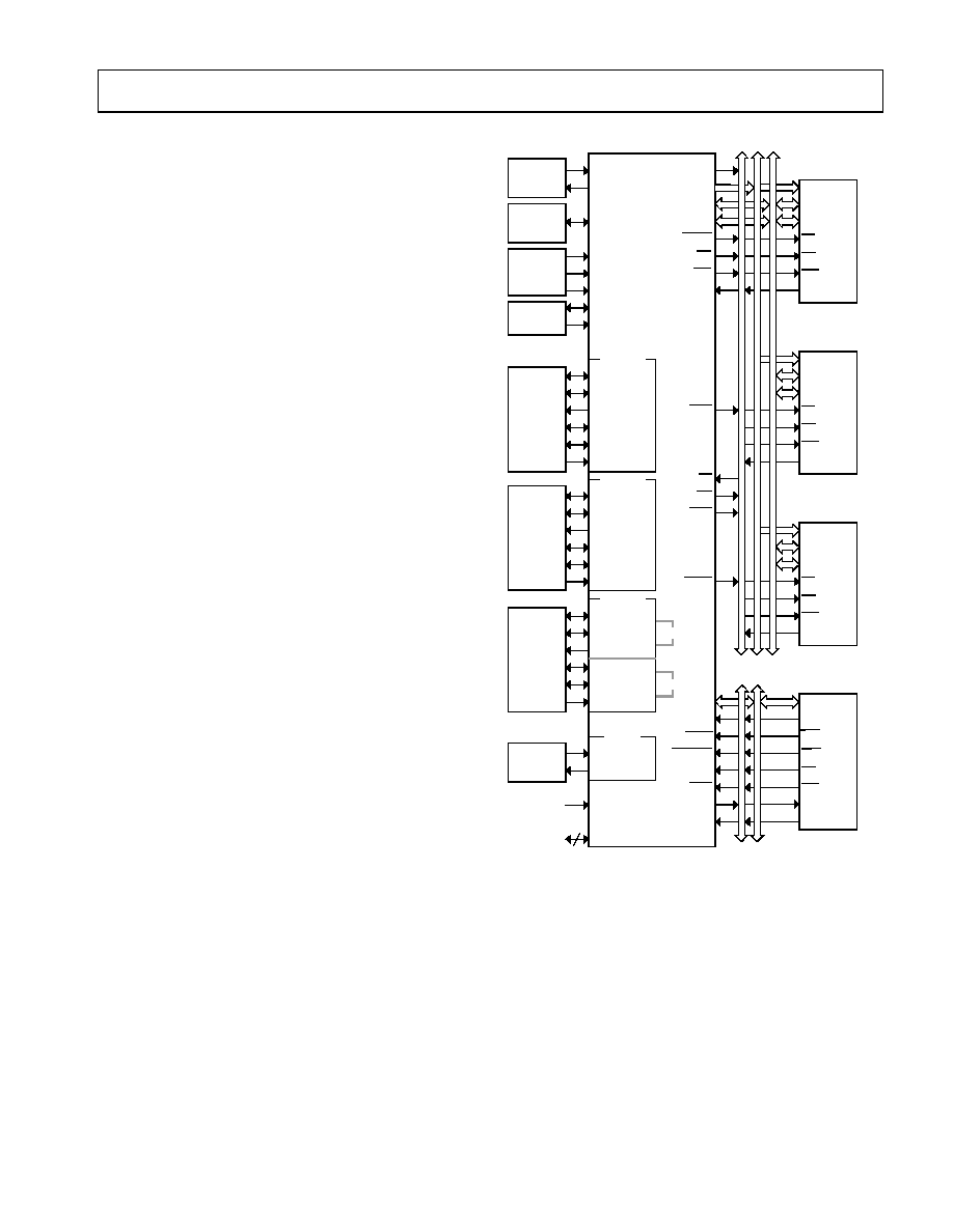
Figure 1. ADSP-2195 System Diagram
6 ( 5 , $ /
' ( 9 , & (
2 3 7 , 2 1 $ /
' $ 7 $ ±
,2 0 6
$ ' 6 3
% 0 6
0 6 ±
% 5
% *
$ & .
: 5
5 '
$ ' ' 5 ±
' $ 7 $ ±
' $ 7 $ ±
$ ' ' 5 ±
' $ 7 $ ±
& 6
$ & .
: (
2 (
( ; 7 ( 5 1 $ /
0 ( 0 2 5 <
2 3 7 , 2 1 $ /
' $ 7 $ ±
$ ' ' 5 ±
' $ 7 $ ±
& 6
$ & .
: (
2 (
% 2 2 7
0 ( 0 2 5 <
2 3 7 , 2 1 $ /
' $ 7 $ ±
$ ' ' 5 ±
' $ 7 $ ±
& 6
$ & .
: (
2 (
( ; 7 ( 5 1 $ /
, 2 0 ( 0 2 5 <
2 3 7 , 2 1 $ /
$
'
'
5
(
6
6
&
2
1
7
5
2
/
'
$
7
$
$ ' ' 5
$ ' ' 5 ±
' $ 7 $ ±
& 6
$ & .
: 5
5 '
+ 2 6 7
3 5 2 & ( 6 6 2 5
2 3 7 , 2 1 $ /
& 6
$ / (
+ $ ' ±
+ $
+ & 0 6
+ & , 2 0 6
+ 5 '
+ : 5
+ $ & .
+ $ / (
+ $ & . B 3
7 & / .
7 ) 6
' 7
5 & / .
5 ) 6
' 5
7 & / .
7 ) 6
' 7
5 & / .
5 ) 6
' 5
7 & / . 6 & .
7 ) 6 0 2 6 ,
' 7 0 , 6 2
5 & / . 6 & .
5 ) 6 0 2 6 ,
' 5 0 , 6 2
5 ; '
7 ; '
5 ( 6 ( 7
- 7 $ *
6 3 2 5 7
6 3 2 5 7
6 3 2 5 7
& / . , 1
; 7 $ /
0 6 ( / ± 3 ) ±
' ) 3 )
% < 3 $ 6 6
% 0 2 ' ( ±
2 3 0 2 ' (
& / . 2 8 7
7 0 5 ±
8 $ 5 7
6 3 ,
6 3 ,
6 ( 5 , $ /
' ( 9 , & (
2 3 7 , 2 1 $ /
6 ( 5 , $ /
' ( 9 , & (
2 3 7 , 2 1 $ /
8 $ 5 7
' ( 9 , & (
2 3 7 , 2 1 $ /
& / 2 & .
2 5
& 5 < 6 7 $ /
7 , 0 ( 5
2 8 7 2 5
& $ 3 7 8 5 (
& / 2 & .
0 8 / 7 ,3 / <
$ 1 '
5 $ 1 * (
% 2 2 7
$ 1 ' 2 3
0 2 ' (
% * +

For current information contact Analog Devices at 800/262-5643
ADSP-2195
September 2001
This information applies to a product under development. Its characteristics and specifications are subject to change with-
out notice. Analog Devices assumes no obligation regarding future manufacturing unless otherwise agreed to in writing.
6
REV. PrA
35(/,0,1$5< 7(&+1,&$/ '$7$
a peripheral to one of the 12 user-defined interrupts. These
assignments determine the priority of each peripheral for
interrupt service.
There are three serial ports on the ADSP-2195 that provide
a complete synchronous, full-duplex serial interface. This
interface includes optional companding in hardware and a
wide variety of framed or frameless data transmit and receive
modes of operation. Each serial port can transmit or receive
an internal or external, programmable serial clock and
frame syncs. Each serial port supports 128-channel Time
Division Multiplexing.
The ADSP-2195 provides up to sixteen general-purpose
I/O pins, which are programmable as either inputs or
outputs. Eight of these pins are dedicated general purpose
Programmable Flag pins. The other eight of them are mul-
tifunctional pins, acting as general purpose I/O pins when
the DSP connects to an 8-bit external data bus and acting
as the upper eight data pins when the DSP connects to a
16-bit external data bus. These Programmable Flag pins can
implement edge- or level-sensitive interrupts, some of which
can be used to base the execution of conditional
instructions.
Three programmable interval timers generate periodic
interrupts. Each timer can be independently set to operate
in one of three modes:
· Pulse Waveform Generation mode
· Pulsewidth Count/Capture mode
· External Event Watchdog mode
Each timer has one bi-directional pin and four registers that
implement its mode of operation: A 7-bit configuration
register, a 32-bit count register, a 32-bit period register, and
a 32-bit pulsewidth register. A single status register supports
all three timers. A bit in the mode status register globally
enables or disables all three timers, and a bit in each timer's
configuration register enables or disables the corresponding
timer independently of the others.
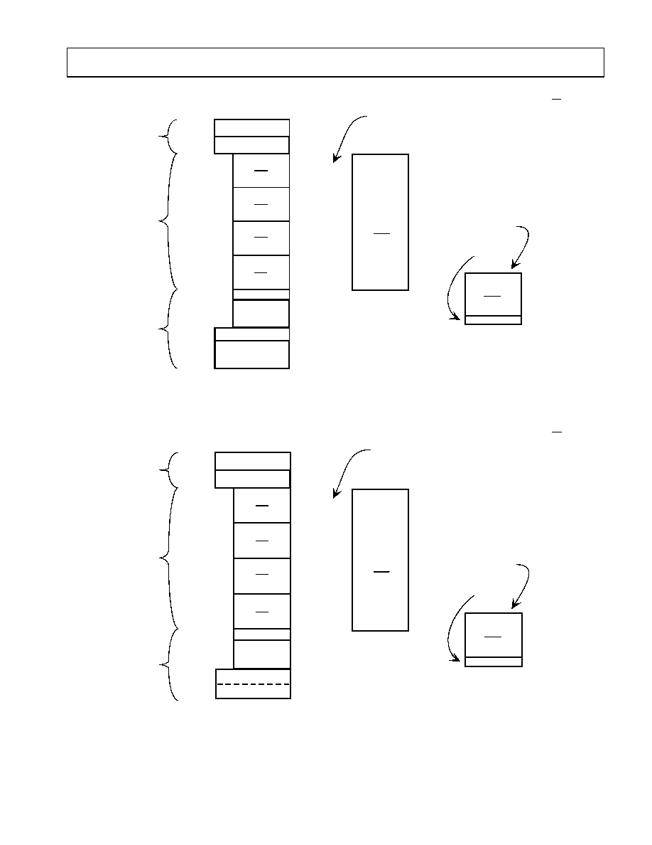
Memory Architecture
The ADSP-2195 DSP provides 32K words of on-chip
SRAM memory. This memory is divided into two 16K
blocks located on memory Page 0 in the DSP's memory
map. The DSP also provides 16K words of on-chip ROM.
In addition to the internal and external memory space, the
ADSP-2195 can address two additional and separate
off-chip memory spaces: I/O space and boot space.
As shown in
Figure 2
, the DSP's two internal memory
blocks populate all of Page 0. The entire DSP memory map
consists of 256 pages (Pages 0
-
255), and each page is 64K
words long. External memory space consists of four
memory banks (banks 03) and supports a wide variety of
SRAM memory devices. Each bank is selectable using the
memory select pins (MS30) and has configurable page
boundaries, waitstates, and waitstate modes. The 1K word
of on-chip boot-ROM populates the top of Page 255 while
the remaining 254 pages are addressable off-chip. I/O
memory pages differ from external memory pages in that
I/O pages are 1K word long, and the external I/O pages have
their own select pin (IOMS). Pages 031 of I/O memory
space reside on-chip and contain the configuration registers
for the peripherals. Both the ADSP-2195 and DMA-capa-
ble peripherals can access the DSP's entire memory map.
Internal (On-Chip) Memory
The ADSP-2195's unified program and data memory space
consists of 16M locations that are accessible through two
24-bit address buses, the PMA and DMA buses. The DSP
uses slightly different mechanisms to generate a 24-bit
address for each bus. The DSP has three functions that
support access to the full memory map.
· The DAGs generate 24-bit addresses for data fetches from
the entire DSP memory address range. Because DAG
index (address) registers are 16 bits wide and hold the
lower 16 bits of the address, each of the DAGs has its own
8-bit page register (DMPGx) to hold the most significant
eight address bits. Before a DAG generates an address,
the program must set the DAG's DMPGx register to the
appropriate memory page.
· The Program Sequencer generates the addresses for
instruction fetches. For relative addressing instructions,
the program sequencer bases addresses for relative jumps,
calls, and loops on the 24-bit Program Counter (PC). In
direct addressing instructions (two-word instructions),
the instruction provides an immediate 24-bit address
value. The PC allows linear addressing of the full 24-bit
address range.
· For indirect jumps and calls that use a 16-bit DAG
address register for part of the branch address, the
Program Sequencer relies on an 8-bit Indirect Jump page
(IJPG) register to supply the most significant eight
address bits. Before a cross page jump or call, the program
must set the program sequencer's IJPG register to the
appropriate memory page.
The ADSP-2195 has 1K word of on-chip ROM that holds
boot routines. If peripheral booting is selected, the DSP
starts executing instructions from the on-chip boot ROM,
which starts the boot process from the selected peripheral.
For more information, see Booting Modes on page 15.
The
on-chip boot ROM is located on Page 255 in the DSP's
memory space map.
Internal On-Chip ROM
The ADSP-2195 DSP features a 16K-word × 24-bit
on-chip maskable ROM mapped into program memory
space (
Figure 3
).
Customers can arrange to have the ROM programmed with
application-specific code.
This information applies to a product under development. Its characteristics and specifications are subject to change with-
out notice. Analog Devices assumes no obligation regarding future manufacturing unless otherwise agreed to in writing.
7
REV. PrA
For current information contact Analog Devices at 800/262-5643
ADSP-2195
September 2001
35(/,0,1$5< 7(&+1,&$/ '$7$
On-Chip Memory Security
The ADSP-2195 has a maskable option to protect the
contents of on-chip memories from being accessed. When
the ROM protection is set, the on-chip ROM space cannot
be accessed by a hardware emulator.
Figure 2. ADSP-2195 Memory Map
Figure 3. ADSP-2195 Memory Map, with On-Chip ROM
%$1.
06
%$1.
06
%$1.
06
%$1.
06
5(6(59('
5(6(59('
%227 52 0 %,7
[
[
[
[
[
[&
[))
[)) )
[)) ))))
$''5(66
[ &
[
. :25'
0(025<
3$*(6
3$*(
3$*(6 ±
3$*(6 ±
3$*(6 ±
3$*(6 ±
3$*(
,17(51$/
0(025<
,17(51$/
0(025<
(;7(51$/
0(025<
%,7
5(6(59('
%/
2&
.
%/
2&
.
.
65$0
.
65$0
0(02 5< 6(/(&76 06
)25 32 57,2 16 2)
7+( 0(02 5< 0$3
$33($5 :,7+ 7+(
6(/(&7(' 0(0 25<
%227
0(025<
%,7
%06
. :25'
3$*(6 ±
[
[)( ))))
,2 0(025<
%,7
. :25'
3$*(6 ±
. :25'
3$*(6 ±
/2:(5 3$*( %2 81'$5,(6
$5( &21),*85$%/( )25
%$1.6 2) (;7(51$/ 0(025<
%281'$5,(6 6+2:1 $5(
%$1. 6,=(6 $7 5(6(7
[
[
[ ))))
$''5(66
$''5(66
,17(51$/
(;7(51$/
,20 6
%$1.
06
%$1.
06
%$1.
06
%$1.
06
5(6(59('
%227 520 %,7
[
[
[
[
[
[&
[))
[)) )
[)) ))))
$''5(66
[ &
[
. :25'
0(025<
3$*(6
3$*(
3$*(6 ±
3$*(6 ±
3$*(6 ±
3$*(6 ±
3$*(
,17(51$/
0(025<
,17(51$/
0(025<
(;7(51$/
0(025<
%,7
5(6(59('
%/
2&
.
%/
2&
.
.
65$0
.
65$0
.
520
0(025< 6(/(&76 06
)25 3257,216 2)
7+( 0(025< 0$3
$33($5 :,7+ 7+(
6(/(&7(' 0(025<
%227
0(025<
%,7
%06
. :25'
3$*(6 ±
[
[)( ))))
,2 0(025<
%,7
. :25'
3$*(6 ±
. :25'
3$*(6 ±
/2:(5 3$*( %281'$5,(6
$5( &21),*85$%/( )25
%$1.6 2) (;7(51$/ 0(025<
%281'$5,(6 6+2:1 $5(
%$1. 6,=(6 $7 5(6(7
[
[
[ ))))
$''5(66
$''5(66
,17(51$/
(;7(51$/
,206
For current information contact Analog Devices at 800/262-5643
ADSP-2195
September 2001
This information applies to a product under development. Its characteristics and specifications are subject to change with-
out notice. Analog Devices assumes no obligation regarding future manufacturing unless otherwise agreed to in writing.
8
REV. PrA
35(/,0,1$5< 7(&+1,&$/ '$7$
External (Off-Chip) Memory
Each of the ADSP-2195's off-chip memory spaces has a
separate control register, so applications can configure
unique access parameters for each space. The access param-
eters include read and write wait counts, waitstate
completion mode, I/O clock divide ratio, write hold time
extension, strobe polarity, and data bus width. The core
clock and peripheral clock ratios influence the external
memory access strobe widths.
For more information, see
Clock Signals on page 14.
The off-chip memory spaces are:
· External memory space (MS30 pins)
· I/O memory space (IOMS pin)
· Boot memory space (BMS pin)
All of these off-chip memory spaces are accessible through
the External Port, which can be configured for 8-bit or
16-bit data widths.
External Memory Space
External memory space consists of four memory banks.
These banks can contain a configurable number of 64K
word pages. At reset, the page boundaries for external
memory have Bank0 containing pages 1
-
63, Bank1 con-
taining pages 64
-
127, Bank2 containing pages 128
-
191,
and Bank3 containing Pages 192
-
254. The MS30
memory bank pins select Banks 30, respectively. The
external memory interface decodes the 8 MSBs of the DSP
program address to select one of the four banks. Both the
ADSP-219x core and DMA-capable peripherals can access
the DSP's external memory space.
I/O Memory Space
The ADSP-2195 supports an additional external memory
called I/O memory space. This space is designed to support
simple connections to peripherals (such as data converters
and external registers) or to bus interface ASIC data regis-
ters. I/O space supports a total of 256K locations. The first
8K addresses are reserved for on-chip peripherals. The
upper 248K addresses are available for external peripheral
devices. The DSP's instruction set provides instructions for
accessing I/O space. These instructions use an 18-bit
address that is assembled from an 8-bit I/O page (IOPG)
register and a 10-bit immediate value supplied in the
instruction. Both the ADSP-219x core and a Host (through
the Host Port Interface) can access I/O memory space.
Boot Memory Space
Boot memory space consists of one off-chip bank with 254
pages. The BMS memory bank pin selects boot memory
space. Both the ADSP-219x core and DMA-capable
peripherals can access the DSP's off-chip boot memory
space. After reset, the DSP always starts executing instruc-
tions from the on-chip boot ROM. Depending on the boot
configuration, the boot ROM code can start booting the
DSP from boot memory.
For more information, see Booting
Modes on page 15.
Interrupts
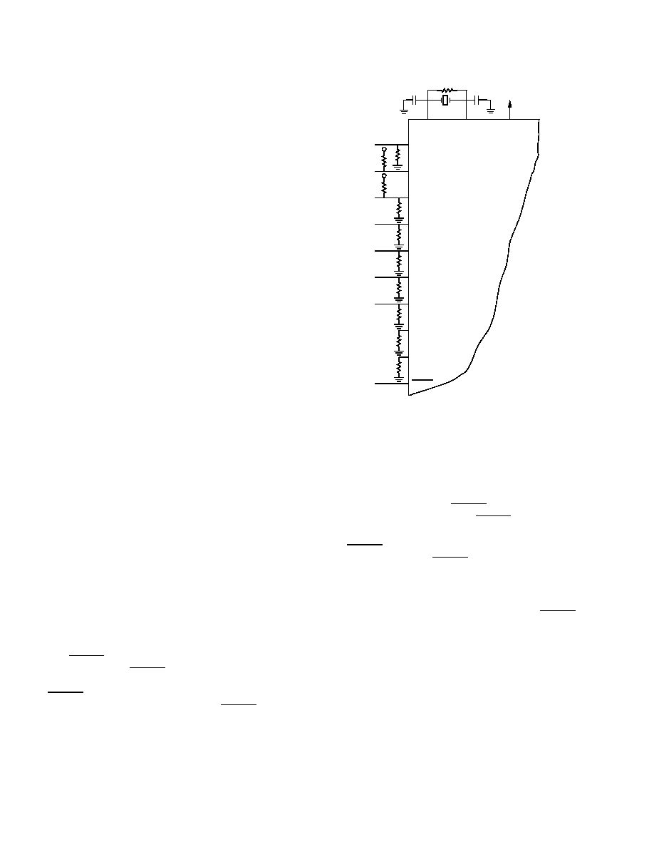
The interrupt controller lets the DSP respond to 17 inter-
rupts with minimum overhead. The controller implements
an interrupt priority scheme as shown in
Table 1
. Applica-
tions can use the unassigned slots for software and
peripheral interrupts.
Table 2
shows the ID and priority at reset of each of the
peripheral interrupts. To assign the peripheral interrupts a
different priority, applications write the new priority to their
corresponding control bits (determined by their ID) in the
Interrupt Priority Control register. The peripheral inter-
rupt's position in the IMASK and IRPTL register and its
vector address depend on its priority level, as shown in
Table 1
. Because the IMASK and IRPTL registers are
limited to 16 bits, any peripheral interrupts assigned a
Table 1. Interrupt Priorities/Addresses
Interrupt
IMASK/
IRPTL
Vector
Address
1
1
These interrupt vectors start at address 0x10000 when the DSP is in
"no-boot", run-form-external memory mode.
Emulator (NMI)--
Highest Priority
NA
NA
Reset (NMI)
0
0x00 0000
Power-Down (NMI)
1
0x00 0020
Loop and PC Stack
2
0x00 0040
Emulation Kernel
3
0x00 0060
User Assigned Interrupt
4
0x00 0080
User Assigned Interrupt
5
0x00 00A0
User Assigned Interrupt
6
0x00 00C0
User Assigned Interrupt
7
0x00 00E0
User Assigned Interrupt
8
0x00 0100
User Assigned Interrupt
9
0x00 0120
User Assigned Interrupt
10
0x00 0140
User Assigned Interrupt
11
0x00 0160
User Assigned Interrupt
12
0x00 0180
User Assigned Interrupt
13
0x00 01A0
User Assigned Interrupt
14
0x00 01C0
User Assigned Interrupt--
Lowest Priority
15
0x00 01E0

This information applies to a product under development. Its characteristics and specifications are subject to change with-
out notice. Analog Devices assumes no obligation regarding future manufacturing unless otherwise agreed to in writing.
9
REV. PrA
For current information contact Analog Devices at 800/262-5643
ADSP-2195
September 2001
35(/,0,1$5< 7(&+1,&$/ '$7$
priority level of 11 are aliased to the lowest priority bit
position (15) in these registers and share vector address
0x00 01E0.
Interrupt routines can either be nested with higher priority
interrupts taking precedence or processed sequentially.
Interrupts can be masked or unmasked with the IMASK
register. Individual interrupt requests are logically ANDed
with the bits in IMASK; the highest priority unmasked
interrupt is then selected. The emulation, power-down, and
reset interrupts are nonmaskable with the IMASK register,
but software can use the DIS INT instruction to mask the
power-down interrupt.
The Interrupt Control (ICNTL) register controls interrupt
nesting and enables or disables interrupts globally. The gen-
eral-purpose Programmable Flag (PFx) pins can be
configured as outputs, can implement software interrupts,
and (as inputs) can implement hardware interrupts. Pro-
grammable Flag pin interrupts can be configured for
level-sensitive, single edge-sensitive, or dual edge-
sensitive operation.
The IRPTL register is used to force and clear interrupts.
On-chip stacks preserve the processor status and are auto-
matically maintained during interrupt handling. To support
interrupt, loop, and subroutine nesting, the PC stack is
33 levels deep, the loop stack is eight levels deep, and the
status stack is 16 levels deep. To prevent stack overflow, the
PC stack can generate a stack-level interrupt if the PC stack
falls below three locations full or rises above 28
locations full.
The following instructions globally enable or disable
interrupt servicing, regardless of the state of IMASK.
ENA INT;
DIS INT;
At reset, interrupt servicing is disabled.
For quick servicing of interrupts, a secondary set of DAG
and computational registers exist. Switching between the
primary and secondary registers lets programs quickly
service interrupts, while preserving the DSP's state.
DMA Controller
The ADSP-2195 has a DMA controller that supports
automated data transfers with minimal overhead for the
DSP core. Cycle stealing DMA transfers can occur between
the ADSP-2195's internal memory and any of its
DMA-capable peripherals. Additionally, DMA transfers
can be accomplished between any of the DMA-capable
peripherals and external devices connected to the external
memory interface. DMA-capable peripherals include the
Host port, SPORTs, SPI ports, and UART. Each individual
DMA-capable peripheral has a dedicated DMA channel. To
describe each DMA sequence, the DMA controller uses a
Table 2. Peripheral Interrupts and Priority at Reset
Interrupt
ID
Reset
Priority
Slave DMA/Host Port Interface
0
0
SPORT0 Receive
1
1
SPORT0 Transmit
2
2
SPORT1 Receive
3
3
SPORT1 Transmit
4
4
SPORT2 Receive/SPI0
5
5
SPORT2 Transmit/SPI1
6
6
UART Receive
7
7
UART Transmit
8
8
Timer A
9
9
Timer B
10
10
Timer C
11
11
Programmable Flag 0 (any PFx)
12
11
Programmable Flag 1 (any PFx)
13
11
Memory DMA port
14
11
Table 3. Interrupt Control (ICNTL) Register Bits
Bit
Description
03
Reserved
4
Interrupt Nesting Enable
5
Global Interrupt Enable
6
Reserved
7
MAC-Biased Rounding Enable
89
Reserved
10
PC Stack Interrupt Enable
11
Loop Stack Interrupt Enable
1215
Reserved
For current information contact Analog Devices at 800/262-5643
ADSP-2195
September 2001
This information applies to a product under development. Its characteristics and specifications are subject to change with-
out notice. Analog Devices assumes no obligation regarding future manufacturing unless otherwise agreed to in writing.
10
REV. PrA
35(/,0,1$5< 7(&+1,&$/ '$7$
set of parameters--called a DMA descriptor. When succes-
sive DMA sequences are needed, these DMA descriptors
can be linked or chained together, so the completion of one
DMA sequence auto-initiates and starts the next sequence.
DMA sequences do not contend for bus access with the DSP
core, instead DMAs "steal" cycles to access memory.
All DMA transfers use the DMA bus shown in the func-
tional block diagram
on page 1
. Because all of the
peripherals use the same bus, arbitration for DMA bus
access is needed. The arbitration for DMA bus access
appears in
Table 4
.
Host Port
The ADSP-2195's Host port functions as a slave on the
external bus of an external Host. The Host port interface
lets a Host read from or write to the DSP's memory space,
boot space, or internal I/O space. Examples of Hosts include
external microcontrollers, microprocessors, or ASICs.
The Host port is a multiplexed address and data bus that
provides both an 8-bit and a 16-bit data path and operates
using an asynchronous transmission protocol. Through this
port, an off-chip Host can directly access the DSP's entire
memory space map, boot memory space, and internal I/O
space. To access the DSP's internal memory space, a Host
steals one cycle per access from the DSP. A Host access to
the DSP's external memory uses the external port interface
and does not stall (or steal cycles from) the DSP's core.
Because a Host can access internal I/O memory space, a
Host can control any of the DSP's I/O mapped peripherals.
The Host port is most efficient when using the DSP as a
slave and uses DMA to automate the incrementing of
addresses for these accesses. In this case, an address does
not have to be transferred from the Host for every
data transfer.
Host Port Acknowledge (HACK) Modes
The Host port supports a number of modes (or protocols)
for generating a HACK output for the host. The host selects
ACK or Ready Modes using the HACK_P and HACK pins.
The Host port also supports two modes for address control:
Address Latch Enable (ALE) and Address Cycle Control
(ACC) modes. The DSP auto-detects ALE versus ACC
Mode from the HALE and HWR inputs.
The host port HACK signal polarity is selected (only at
reset) as active high or active low, depending on the value
driven on the HACK_P pin.The HACK polarity is stored
into the host port configuration register as a read only bit.
The DSP uses HACK to indicate to the Host when to
complete an access. For a read transaction, a Host can
proceed and complete an access when valid data is present
in the read buffer and the host port is not busy doing a write.
For a write transactions, a Host can complete an access
when the write buffer is not full and the host port is not busy
doing a write.
Two mode bits in the Host Port configuration register
HPCR [7:6] define the functionality of the HACK line.
HPCR6 is initialized at reset based on the values driven on
HACK and HACK_P pins (shown in
Table 5
); HPCR7 is
always cleared (0) at reset. HPCR [7:6] can be modified
after reset by a write access to the host port
configuration register.
Table 4. I/O Bus Arbitration Priority
DMA Bus Master
Arbitration Priority
SPORT0 Receive DMA
0--Highest
SPORT1 Receive DMA
1
SPORT2 Receive DMA
2
SPORT0 Transmit DMA
3
SPORT1 Transmit DMA
4
SPORT2 Transmit DMA
5
SPI0 Receive/Transmit DMA
6
SPI1 Receive/Transmit DMA
7
UART Receive DMA
8
UART Transmit DMA
9
Host Port DMA
10
Memory DMA
11--Lowest
Table 5. Host Port Acknowledge Mode Selection
Values Driven At
Reset
HPCR [7:6]
Initial Values
Acknowledge
Mode
HACK_P
HACK
Bit 7
Bit 6
0
0
0
1
Ready Mode
0
1
0
0
ACK Mode
1
0
0
0
ACK Mode
1
1
0
1
Ready Mode

This information applies to a product under development. Its characteristics and specifications are subject to change with-
out notice. Analog Devices assumes no obligation regarding future manufacturing unless otherwise agreed to in writing.
11
REV. PrA
For current information contact Analog Devices at 800/262-5643
ADSP-2195
September 2001
35(/,0,1$5< 7(&+1,&$/ '$7$
The functional modes selected by HPCR [7:6] are as follows
(assuming active high signal):
· ACK Mode--Acknowledge is active on strobes; HACK
goes high from the leading edge of the strobe to indicate
when the access can complete. After the Host samples the
HACK active, it can complete the access by removing the
strobe.The host port then removes the HACK.
· Ready Mode--Ready active on strobes, goes low to insert
wait state during the access.If the host port can not
complete the access, it de-asserts the HACK/READY
line. In this case, the Host has to extend the access by
keeping the strobe asserted. When the Host samples the
HACK asserted, it can then proceed and complete the
access by de-asserting the strobe.
While in Address Cycle Control (ACC) mode and the ACK
or Ready acknowledge modes, the HACK is returned active
for any address cycle.
Host Port Chip Selects
There are two chip-select signals associated with the Host
Port: HCMS and HCIOMS. The Host Chip Memory
Select (HCMS) lets the Host select the DSP and directly
access the DSP's internal/external memory space or boot
memory space. The Host Chip I/O Memory Select
(HCIOMS) lets the Host select the DSP and directly access
the DSP's internal I/O memory space.
Before starting a direct access, the Host configures Host
port interface registers, specifying the width of external data
bus (8- or 16-bit) and the target address page (in the IJPG
register). The DSP generates the needed memory select
signals during the access, based on the target address. The
Host port interface combines the data from one, two, or
three consecutive Host accesses (up to one 24-bit value) into
a single DMA bus access to prefetch Host direct reads or to
post direct writes. During assembly of larger words, the Host
port interface asserts ACK for each byte access that does
not start a read or complete a write. Otherwise, the Host
port interface asserts ACK when it has completed the
memory access successfully.
DSP Serial Ports (SPORTs)
The ADSP-2195 incorporates three complete synchronous
serial ports (SPORT0, SPORT1, and SPORT2) for serial
and multiprocessor communications. The SPORTs
support the following features:
· Bidirectional operation--each SPORT has independent
transmit and receive pins.
· Buffered (8-deep) transmit and receive ports--each port
has a data register for transferring data words to and from
other DSP components and shift registers for shifting data
in and out of the data registers.
· Clocking--each transmit and receive port can either use
an external serial clock (
75 MHz) or generate its own,
in frequencies ranging from 1144 Hz to 75 MHz.
· Word length--each SPORT supports serial data words
from 3 to 16 bits in length transferred in Big Endian
(MSB) or Little Endian (LSB) format.
· Framing--each transmit and receive port can run with or
without frame sync signals for each data word. Frame sync
signals can be generated internally or externally, active
high or low, and with either of two pulsewidths and early
or late frame sync.
· Companding in hardware--each SPORT can perform
A-law or µ-law companding according to ITU recommen-
dation G.711. Companding can be selected on the
transmit and/or receive channel of the SPORT without
additional latencies.
· DMA operations with single-cycle overhead--each
SPORT can automatically receive and transmit multiple
buffers of memory data, one data word each DSP cycle.
Either the DSP's core or a Host processor can link or chain
sequences of DMA transfers between a SPORT and
memory. The chained DMA can be dynamically allocated
and updated through the DMA descriptors (DMA
transfer parameters) that set up the chain.
· Interrupts--each transmit and receive port generates an
interrupt upon completing the transfer of a data word or
after transferring an entire data buffer or buffers through
DMA.
· Multichannel capability--each SPORT supports the
H.100 standard.
Serial Peripheral Interface (SPI) Ports
The DSP has two SPI-compatible ports that enable the DSP
to communicate with multiple SPI-compatible devices.
These ports are multiplexed with SPORT2, so either
SPORT2 or the SPI ports are active, depending on the state
of the OPMODE pin during hardware reset.
The SPI interface uses three pins for transferring data: two
data pins (Master Output-Slave Input, MOSIx, and Master
Input-Slave Output, MISOx) and a clock pin (Serial Clock,
SCKx). Two SPI chip select input pins (SPISSx) let other
SPI devices select the DSP, and fourteen SPI chip select
output pins (SPIxSEL71) let the DSP select other SPI
devices. The SPI select pins are reconfigured Programmable
Flag pins. Using these pins, the SPI ports provide a full
duplex, synchronous serial interface, which supports both
master and slave modes and multimaster environments.
Each SPI port's baud rate and clock phase/polarities are
programmable (see
Figure 4
), and each has an integrated
DMA controller, configurable to support both transmit and
receive data streams. The SPI's DMA controller can only
service unidirectional accesses at any given time.
Figure 4. SPI Clock Rate Calculation
SPI Clock Rate
HCLK
2 SPIBAUD
×
--------------------------------------
=

For current information contact Analog Devices at 800/262-5643
ADSP-2195
September 2001
This information applies to a product under development. Its characteristics and specifications are subject to change with-
out notice. Analog Devices assumes no obligation regarding future manufacturing unless otherwise agreed to in writing.
12
REV. PrA
35(/,0,1$5< 7(&+1,&$/ '$7$
During transfers, the SPI ports simultaneously transmit and
receive by serially shifting data in and out on their two serial
data lines. The serial clock line synchronizes the shifting and
sampling of data on the two serial data lines.
In master mode, the DSP's core performs the following
sequence to set up and initiate SPI transfers:
1.
Enables and configures the SPI port's operation (data
size, and transfer format).
2.
Selects the target SPI slave with an SPIxSELy output
pin (reconfigured Programmable Flag pin).
3.
Defines one or more DMA descriptors in Page 0 of I/O
memory space (optional in DMA mode only).
4.
Enables the SPI DMA engine and specifies transfer
direction (optional in DMA mode only).
5.
In non-DMA mode only, reads or writes the SPI port
receive or transmit data buffer.
The SCKx line generates the programmed clock pulses
for simultaneously shifting data out on MOSIx and
shifting data in on MISOx. In DMA mode only, transfers
continue until the SPI DMA word count transitions
from 1 to 0.
In slave mode, the DSP's core performs the following
sequence to set up the SPI port to receive data from a master
transmitter:
1.
Enables and configures the SPI slave port to match the
operation parameters set up on the master (data size
and transfer format) SPI transmitter.
2.
Defines and generates a receive DMA descriptor in
Page 0 of memory space to interrupt at the end of the
data transfer (optional in DMA mode only).
3.
Enables the SPI DMA engine for a receive access
(optional in DMA mode only).
4.
Starts receiving the data on the appropriate SPI SCKx
edges after receiving an SPI chip select on an SPISSx
input pin (reconfigured Programmable Flag pin)
from a master
In DMA mode only, reception continues until the SPI
DMA word count transitions from 1 to 0. The DSP's core
could continue, by queuing up the next DMA descriptor.
A slave mode transmit operation is similar, except the DSP's
core specifies the data buffer in memory space from which
to transmit data, generates and relinquishes control of the
transmit DMA descriptor, and begins filling the SPI port's
data buffer. If the SPI controller isn't ready on time to
transmit, it can transmit a "zero" word.
UART Port
The UART port provides a simplified UART interface to
another peripheral or Host. It performs full duplex, asyn-
chronous transfers of serial data. Options for the UART
include support for 58 data bits; 1 or 2 stop bits; and none,
even, or odd parity. The UART port supports two modes
of operation:
· PIO (programmed I/O)
The DSP's core sends or receives data by writing or
reading I/O-mapped UATX or UARX registers, respec-
tively. The data is double-buffered on both transmit and
receive.
· DMA (direct memory access)
The DMA controller transfers both transmit and receive
data. This reduces the number and frequency of inter-
rupts required to transfer data to and from memory. The
UART has two dedicated DMA channels. These DMA
channels have lower priority than most DMA channels
because of their relatively low service rates.
The UART's baud rate (see
Figure 5
), serial data format,
error code generation and status, and interrupts are
programmable:
· Supported bit rates range from 95 bits to 6.25M bits per
second (100 MHz peripheral clock).
· Supported data formats are 7- or 12-bit frames.
· Transmit and receive status can be configured to generate
maskable interrupts to the DSP's core.
The timers can be used to provide a hardware-assisted
autobaud detection mechanism for the UART interface.
Programmable Flag (PFx) Pins
The ADSP-2195 has 16 bidirectional, general-purpose I/O,
Programmable Flag (PF150) pins. The PF70 pins are
dedicated to general-purpose I/O. The PF158 pins serve
either as general-purpose I/O pins (if the DSP is connected
to an 8-bit external data bus) or serve as DATA158 lines
(if the DSP is connected to a 16-bit external data bus). The
Programmable Flag pins have special functions for clock
multiplier selection and for SPI port operation. For more
information, see
Serial Peripheral Interface (SPI) Ports on
Figure 5. UART Clock Rate Calculation
1
1
Where D = 1 to 65536
UART Clock Rate
HCLK
16 D
×
------------------
=

This information applies to a product under development. Its characteristics and specifications are subject to change with-
out notice. Analog Devices assumes no obligation regarding future manufacturing unless otherwise agreed to in writing.
13
REV. PrA
For current information contact Analog Devices at 800/262-5643
ADSP-2195
September 2001
35(/,0,1$5< 7(&+1,&$/ '$7$
page 11
and
Clock Signals on page 14
. Ten mem-
ory-mapped registers control operation of the
Programmable Flag pins:
· Flag Direction register
Specifies the direction of each individual PFx pin as input
or output.
· Flag Control and Status registers
Specify the value to drive on each individual PFx output
pin. As input, software can predicate instruction
execution on the value of individual PFx input pins
captured in this register. One register sets bits, and one
register clears bits.
· Flag Interrupt Mask registers
Enable and disable each individual PFx pin to function
as an interrupt to the DSP's core. One register sets bits to
enable interrupt function, and one register clears bits to
disable interrupt function. Input PFx pins function as
hardware interrupts, and output PFx pins function as
software interrupts--latching in the IMASK and IRPTL
registers.
· Flag Interrupt Polarity register
Specifies the polarity (active high or low) for interrupt
sensitivity on each individual PFx pin.
· Flag Sensitivity registers
Specify whether individual PFx pins are level- or
edge-sensitive and specify--if edge-sensitive--whether
just the rising edge or both the rising and falling edges of
the signal are significant. One register selects the type of
sensitivity, and one register selects which edges are signif-
icant for edge-sensitivity.
Low Power Operation
The ADSP-2195 has four low-power options that signifi-
cantly reduce the power dissipation when the device
operates under standby conditions. To enter any of these
modes, the DSP executes an IDLE instruction. The
ADSP-2195 uses configuration of the PDWN, STOPCK,
and STOPALL bits in the PLLCTL register to select
between the low-power modes as the DSP executes the
IDLE. Depending on the mode, an IDLE shuts off clocks
to different parts of the DSP in the different modes. The
low power modes are:
· Idle
· Power-Down Core
· Power-Down Core/Peripherals
· Power-Down All
Idle Mode
When the ADSP-2195 is in Idle mode, the DSP core stops
executing instructions, retains the contents of the instruc-
tion pipeline, and waits for an interrupt. The core clock and
peripheral clock continue running.
To enter Idle mode, the DSP can execute the IDLE instruc-
tion anywhere in code. To exit Idle mode, the DSP responds
to an interrupt and (after two cycles of latency) resumes
executing instructions with the instruction after the IDLE.
Power-down Core Mode
When the ADSP-2195 is in Power-Down Core mode, the
DSP core clock is off, but the DSP retains the contents of
the pipeline and keeps the PLL running. The peripheral bus
keeps running, letting the peripherals receive data.
To enter Power-Down Core mode, the DSP executes an
IDLE instruction after performing the following tasks:
· Enter a power-down interrupt service routine
· Check for pending interrupts and I/O service routines
· Clear (= 0) the PDWN bit in the PLLCTL register
· Clear (= 0) the STOPALL bit in the PLLCTL register
· Set (= 1) the STOPCK bit in the PLLCTL register
To exit Power-Down Core mode, the DSP responds to an
interrupt and (after two cycles of latency) resumes executing
instructions with the instruction after the IDLE.
Power-Down Core/Peripherals Mode
When the ADSP-2195 is in Power-Down Core/Peripherals
mode, the DSP core clock and peripheral bus clock are off,
but the DSP keeps the PLL running. The DSP does not
retain the contents of the instruction pipeline.The periph-
eral bus is stopped, so the peripherals cannot receive data.
To enter Power-Down Core/Peripherals mode, the DSP
executes an IDLE instruction after performing the
following tasks:
· Enter a power-down interrupt service routine
· Check for pending interrupts and I/O service routines
· Clear (= 0) the PDWN bit in the PLLCTL register
· Set (= 1) the STOPALL bit in the PLLCTL register
To exit Power-Down Core/Peripherals mode, the DSP
responds to an interrupt and (after five to six cycles of
latency) resumes executing instructions with the instruction
after the IDLE.
Power-Down All Mode
When the ADSP-2195 is in Power-Down All mode, the
DSP core clock, the peripheral clock, and the PLL are all
stopped. The DSP does not retain the contents of the
instruction pipeline. The peripheral bus is stopped, so the
peripherals cannot receive data.
To enter Power-Down All mode, the DSP executes an IDLE
instruction after performing the following tasks:
· Enter a power-down interrupt service routine
· Check for pending interrupts and I/O service routines
· Set (= 1) the PDWN bit in the PLLCTL register
For current information contact Analog Devices at 800/262-5643
ADSP-2195
September 2001
This information applies to a product under development. Its characteristics and specifications are subject to change with-
out notice. Analog Devices assumes no obligation regarding future manufacturing unless otherwise agreed to in writing.
14
REV. PrA
35(/,0,1$5< 7(&+1,&$/ '$7$
To exit Power-Down Core/Peripherals mode, the DSP
responds to an interrupt and (after 500 cycles to re-stabilize
the PLL) resumes executing instructions with the instruc-
tion after the IDLE.
Clock Signals
The ADSP-2195 can be clocked by a crystal oscillator or a
buffered, shaped clock derived from an external clock oscil-
lator. If a crystal oscillator is used, the crystal should be
connected across the CLKIN and XTAL pins, with two
capacitors connected as shown in
Figure 6
. Capacitor
values are dependent on crystal type and should be specified
by the crystal manufacturer. A parallel-resonant, funda-
mental frequency, microprocessor-grade crystal should be
used for this configuration.
If a buffered, shaped clock is used, this external clock
connects to the DSP's CLKIN pin. CLKIN input cannot
be halted, changed, or operated below the specified
frequency during normal operation. This clock signal
should be a TTL-compatible signal. When an external clock
is used, the XTAL input must be left unconnected.
The DSP provides a user-programmable 1 to 32 multi-
plication of the input clock, including some fractional
values, to support 128 external to internal (DSP core) clock
ratios. The MSEL60, BYPASS, and DF pins decide the
PLL multiplication factor at reset. At runtime, the multipli-
cation factor can be controlled in software. To support input
clocks greater that 100 MHz, the PLL uses an additional
input: the Divide Frequency (DF) pin. If the input clock is
greater than 100 MHz, DF must be high. If the input clock
is less than 100 MHz, DF must be low. The combination of
pullup and pull-down resistors in
Figure 6
set up a core
clock ratio of 6:1, which produces a 150 MHz core clock
from the 25 MHz input. For other clock multiplier settings,
see the ADSP-219x/2191 DSP Hardware Reference.
The peripheral clock is supplied to the CLKOUT pin.
All on-chip peripherals for the ADSP-2195 operate at the
rate set by the peripheral clock. The peripheral clock is
either equal to the core clock rate or one-half the DSP core
clock rate. This selection is controlled by the IOSEL bit in
the PLLCTL register. The maximum core clock
is 160 MHz, and the maximum peripheral clock
is 100 MHz--the combination of the input clock and
core/peripheral clock ratios may not exceed these limits.
Reset
The RESET signal initiates a master reset of the
ADSP-2195. The RESET signal must be asserted during
the power-up sequence to assure proper initialization.
RESET during initial power-up must be held long enough
to allow the internal clock to stabilize. If RESET is activated
any time after power up, the clock does not continue to run
and requires stabilization time when recovering from reset.
The power-up sequence is defined as the total time required
for the crystal oscillator circuit to stabilize after a valid V
DD
is applied to the processor, and for the internal phase-locked
loop (PLL) to lock onto the specific crystal frequency. A
minimum of 100 µs ensures that the PLL has locked, but
does not include the crystal oscillator start-up time. During
this power-up sequence the RESET signal should be held
low. On any subsequent resets, the RESET signal must meet
the minimum pulsewidth specification, t
RSP
.
The RESET input contains some hysteresis. If using an RC
circuit to generate your RESET signal, the circuit should
use an external Schmidt trigger.
The master reset sets all internal stack pointers to the empty
stack condition, masks all interrupts, and resets all registers
to their default values (where applicable). When RESET is
released, if there is no pending bus request and the chip is
configured for booting, the boot-loading sequence is per-
formed. Program control jumps to the location of the
on-chip boot ROM (0xFF0000).
Power Supplies
The ADSP-2195 has separate power supply connections for
the internal (V
DDINT
) and external (V
DDEXT
) power supplies.
The internal supply must meet the 2.5 V requirement. The
external supply must be connected to a 3.3 V supply. All
external supply pins must be connected to the same supply.
Figure 6. External Crystal Connections
&/.,1
&/.287
;7$/
$'63
0 6(/ 3)
0 6(/ 3)
0 6(/ 3)
0 6(/ 3)
0 6(/ 3)
0 6(/ 3)
5(6(7
0 +]
0 6(/ 3)
') 3)
9
' '
9
' '
%<3$66
5(6(7
6285&(
5817,0 (
3) 3,1 ,2
7+( 38//8338//'2: 1
5(6,67256 21 7+(
0 6(/ ') $1' %<3$66
3,16 6(/(&7 7+( &25(
&/2&. 5$7,2
+(5( 7+( 6(/(&7,21
$1' 0 +] ,1387
&/2&. 35 2'8&( $
0 +] &25( &/2& .

This information applies to a product under development. Its characteristics and specifications are subject to change with-
out notice. Analog Devices assumes no obligation regarding future manufacturing unless otherwise agreed to in writing.
15
REV. PrA
For current information contact Analog Devices at 800/262-5643
ADSP-2195
September 2001
35(/,0,1$5< 7(&+1,&$/ '$7$
As indicated in
Table 6
, the OPMODE pin has a dual role,
acting as a boot mode select during reset and determining
SPORT or SPI operation at runtime. If the OPMODE pin
at reset is the opposite of what is needed in an application
during runtime, the application needs to set the OPMODE
bit appropriately during runtime prior to using the corre-
sponding peripheral.
Booting Modes
The ADSP-2195 has seven mechanisms (listed in
Table 6
)
for automatically loading internal program memory
after reset.
The OPMODE, BMODE1, and BMODE0 pins, sampled
during hardware reset, and three bits in the Reset Configu-
ration Register implement these modes:
· Execute from memory external 16 bits--The memory
boot routine located in boot ROM memory space
executes a boot-stream-formatted program located at
address 0x10000 of boot memory space, packing 16-bit
external data into 24-bit internal data. The External Port
Interface is configured for the default clock multiplier
(128) and read waitstates (7).
· Boot from EPROM--The EPROM boot routine located
in boot ROM memory space executes a boot-stream-for-
matted program located at address 0x00000 of boot
memory space, packing 8- or 16-bit external data into
24-bit internal data. The External Port Interface is con-
figured for the default clock multiplier (32) and read
waitstates (7).
· Boot from Host--The (8- or 16-bit) Host downloads a
boot-stream-formatted program to internal or external
memory. The Host's boot routine is located in internal
ROM memory space and uses the top 16 locations of
Page 0 program memory and the top 272 locations of
Page 0 data memory.
The internal boot ROM sets semaphore A (an IO register
within the host port) and then polls until the semaphore
is reset. Once detected, the internal boot ROM will remap
the interrupt vector table to Page 0 internal memory and
jump to address 0x0000 internal. From the point of view
of the host interface, an external host has full control of
the DSP's memory map. The Host has the freedom to
directly write internal memory, external memory, and
internal I/O memory space. The DSP core execution is
held off until the Host clears the semaphore register. This
strategy allows the maximum flexibility for the Host to
boot in the program and data code, by leaving it up to
the programmer.
· Execute from memory external 8 bits (No Boot)--
execution starts from Page 1 of external memory space,
packing either 8- or 16-bit external data into 24-bit
internal data. The External Port Interface is configured
for the default clock multiplier (128) and read waitstates
(7).
· Boot from UART--The Host downloads
boot-stream-formatted program using an autobaud
handshake sequence. The Host agent selects a baud rate
within the UART's clocking capabilities. After a hardware
reset, the DSP's UART transmits 0xFF values (eight bits
data, one start bit, one stop bit, no parity bit) until
detecting the start of the first memory block. The UART
boot routine is located in internal ROM memory space
and uses the top 16 locations of Page 0 program memory
and the top 272 locations of Page 0 data memory.
· Boot from SPI, up to 4K bits--The SPI0 port uses the
SPI0SEL1 (reconfigured PF2) output pin to select a
single serial EPROM device, submits a read command at
address 0x00, and begins clocking consecutive data into
internal or external memory. Use only SPI-compatible
EPROMs of
4K bit (12-bit address range). The SPI0
boot routine located in internal ROM memory space
executes a boot-stream-formatted program, using the top
16 locations of Page 0 program memory and the top 272
locations of Page 0 data memory. The SPI boot configu-
ration is SPIBAUD0=60 (decimal), CPHA=1, CPOL=1,
8-bit data, and MSB first.
· Boot from SPI, from >4K bits to 512K bits--The SPI0
port uses the SPI0SEL1 (re-configured PF2) output pin
to select a single serial EPROM device, submits a read
command at address 0x00, and begins clocking consecu-
tive data into internal or external memory. Use only
SPI-compatible EPROMs of
4K bit (16-bit address
range). The SPI0 boot routine located in internal ROM
memory space executes a boot-stream-formatted
program, using the top 16 locations of Page 0 program
memory and the top 272 locations of Page 0 data memory.
Table 6. Select Boot Mode (OPMODE, BMODE1, and
BMODE0)
OP
M
O
D
E
BM
O
D
E1
BM
O
D
E0
Function
0
0
0
Execute from external memory 16 bits
(No Boot)
0
0
1
Boot from EPROM
0
1
0
Boot from Host
0
1
1
Reserved
1
0
0
Execute from external memory 8 bits
(No Boot)
1
0
1
Boot from UART
1
1
0
Boot from SPI, up to 4K bits
1
1
1
Boot from SPI, >4K bits up to
512K bits

For current information contact Analog Devices at 800/262-5643
ADSP-2195
September 2001
This information applies to a product under development. Its characteristics and specifications are subject to change with-
out notice. Analog Devices assumes no obligation regarding future manufacturing unless otherwise agreed to in writing.
16
REV. PrA
35(/,0,1$5< 7(&+1,&$/ '$7$
Bus Request and Bus Grant
The ADSP-2195 can relinquish control of the data and
address buses to an external device. When the external
device requires access to the bus, it asserts the bus request
(BR) signal. The (BR) signal is arbitrated with core and
peripheral requests. External Bus requests have the lowest
priority. If no other internal request is pending, the external
bus request will be granted. Due to synchronizer and arbi-
tration delays, bus grants will be provided with a minimum
of three peripheral clock delays. The ADSP-2195 will
respond to the bus grant by:
· Three-stating the data and address buses and the MS30,
BMS, IOMS, RD, and WR output drivers.
· Asserting the bus grant (BG) signal.
The ADSP-2195 will halt program execution if the bus is
granted to an external device and an instruction fetch or
data read/write request is made to external general-purpose
or peripheral memory spaces. If an instruction requires two
external memory read accesses, the bus will not be granted
between the two accesses. If an instruction requires an
external memory read and an external memory write access,
the bus may be granted between the two accesses. The
external memory interface can be configured so that the
core will have exclusive use of the interface. DMA and Bus
Requests will be granted. When the external device releases
BR, the DSP releases BG and continues program execution
from the point at which it stopped.
The bus request feature operates at all times, even while the
DSP is booting and RESET is active.
The ADSP-2195 asserts the BGH pin when it is ready to
start another external port access, but is held off because
the bus was previously granted. This mechanism can be
extended to define more complex arbitration protocols for
implementing more elaborate multimaster systems.
Instruction Set Description
The ADSP-2195 assembly language instruction set has an
algebraic syntax that was designed for ease of coding and
readability. The assembly language, which takes full
advantage of the processor's unique architecture, offers the
following benefits:
· ADSP-219x assembly language syntax is a superset of and
source-code-compatible (except for two data registers
and DAG base address registers) with ADSP-218x family
syntax. It may be necessary to restructure ADSP-218x
programs to accommodate the ADSP-2195's unified
memory space and to conform to its interrupt vector map.
· The algebraic syntax eliminates the need to remember
cryptic assembler mnemonics. For example, a typical
arithmetic add instruction, such as AR = AX0 + AY0,
resembles a simple equation.
· Every instruction, but two, assembles into a single, 24-bit
word that can execute in a single instruction cycle. The
exceptions are two dual word instructions. One writes 16-
or 24-bit immediate data to memory, and the other is an
absolute jump/call with the 24-bit address specified in the
instruction.
· Multifunction instructions allow parallel execution of an
arithmetic, MAC, or shift instruction with up to two
fetches or one write to processor memory space during a
single instruction cycle.
· Program flow instructions support a wider variety of con-
ditional and unconditional jumps/calls and a larger set of
conditions on which to base execution of conditional
instructions.
Development Tools
The ADSP-2195 is supported with a complete set of
software and hardware development tools, including Analog
Devices' emulators and VisualDSP++® development envi-
ronment. The same emulator hardware that supports other
ADSP-219x DSPs, also fully emulates the ADSP-2195.
The VisualDSP++ project management environment lets
programmers develop and debug an application. This envi-
ronment includes an easy-to-use assembler that is based on
an algebraic syntax; an archiver (librarian/library builder),
a linker, a loader, a cycle-accurate instruction-level simula-
tor, a C/C++ compiler, and a C/C++ run-time library that
includes DSP and mathematical functions. Two key points
for these tools are:
· Compiled ADSP-219x C/C++ code efficiency--the
compiler has been developed for efficient translation of
C/C++ code to ADSP-219x assembly. The DSP has
architectural features that improve the efficiency of
compiled C/C++ code.
· ADSP-218x family code compatibility--The assembler
has legacy features to ease the conversion of existing
ADSP-218x applications to the ADSP-219x.
Debugging both C/C++ and assembly programs with the
VisualDSP++ debugger, programmers can:
· View mixed C/C++ and assembly code (interleaved
source and object information)
· Insert break points
· Set conditional breakpoints on registers, memory, and
stacks
· Trace instruction execution
· Perform linear or statistical profiling of program
execution
· Fill, dump, and graphically plot the contents of memory
· Source level debugging
· Create custom debugger windows
The VisualDSP++ IDE lets programmers define and
manage DSP software development. Its dialog boxes and
property pages let programmers configure and manage all
This information applies to a product under development. Its characteristics and specifications are subject to change with-
out notice. Analog Devices assumes no obligation regarding future manufacturing unless otherwise agreed to in writing.
17
REV. PrA
For current information contact Analog Devices at 800/262-5643
ADSP-2195
September 2001
35(/,0,1$5< 7(&+1,&$/ '$7$
of the ADSP-219x development tools, including the syntax
highlighting in the VisualDSP++ editor. This capability
permits:
· Control how the development tools process inputs and
generate outputs.
· Maintain a one-to-one correspondence with the tool's
command line switches.
Analog Devices' DSP emulators use the IEEE 1149.1 JTAG
test access port of the ADSP-2195 processor to monitor and
control the target board processor during emulation. The
emulator provides full-speed emulation, allowing inspection
and modification of memory, registers, and processor
stacks. Nonintrusive in-circuit emulation is assured by the
use of the processor's JTAG interface--the emulator does
not affect target system loading or timing.
In addition to the software and hardware development tools
available from Analog Devices, third parties provide a wide
range of tools supporting the ADSP-219x processor family.
Hardware tools include ADSP-219x PC plug-in cards.
Third Party software tools include DSP libraries, real-time
operating systems, and block diagram design tools.
Designing an Emulator-Compatible DSP Board
(Target)
The White Mountain DSP (Product Line of Analog
Devices, Inc.) family of emulators are tools that every DSP
developer needs to test and debug hardware and software
systems. Analog Devices has supplied an IEEE 1149.1
JTAG Test Access Port (TAP) on each JTAG DSP. The
emulator uses the TAP to access the internal features of the
DSP, allowing the developer to load code, set breakpoints,
observe variables, observe memory, and examine registers.
The DSP must be halted to send data and commands, but
once an operation has been completed by the emulator, the
DSP system is set running at full speed with no impact on
system timing.
To use these emulators, the target's design must include the
interface between an Analog Devices' JTAG DSP and the
emulation header on a custom DSP target board.
Target Board Header
The emulator interface to an Analog Devices' JTAG DSP
is a 14-pin header, as shown in
Figure 7
. The customer must
supply this header on the target board in order to commu-
nicate with the emulator. The interface consists of a
standard dual row 0.025" square post header, set on
0.1"
0.1" spacing, with a minimum post length of 0.235".
Pin 3 is the key position used to prevent the pod from being
inserted backwards. This pin must be clipped on the target
board.
Also, the clearance (length, width, and height) around the
header must be considered. Leave a clearance of at least
0.15" and 0.10" around the length and width of the header,
and reserve a height clearance to attach and detach the pod
connector.
As can be seen in
Figure 7
, there are two sets of signals on
the header. There are the standard JTAG signals TMS,
TCK, TDI, TDO, TRST, and EMU used for emulation
purposes (via an emulator). There are also secondary JTAG
signals BTMS, BTCK, BTDI, and BTRST that are option-
ally used for board-level (boundary scan) testing.
When the emulator is not connected to this header, place
jumpers across BTMS, BTCK, BTRST, and BTDI as
shown in
Figure 8
. This holds the JTAG signals in the
correct state to allow the DSP to run free. Remove all the
jumpers when connecting the emulator to the JTAG header.
Figure 7. JTAG Target Board Connector for JTAG
Equipped Analog Devices DSP (Jumpers in
Place)
Figure 8. JTAG Target Board Connector with No Local
Boundary Scan
723 9,(:
(0 8
*1'
70 6
7&.
7567
7',
7'2
*1'
.(< 12 3,1
%70 6
%7& .
%7567
%7',
*1'
723 9,(:
(0 8
*1'
70 6
7&.
7567
7',
7'2
*1'
.(< 12 3,1
%70 6
%7& .
%7567
%7',
*1'
For current information contact Analog Devices at 800/262-5643
ADSP-2195
September 2001
This information applies to a product under development. Its characteristics and specifications are subject to change with-
out notice. Analog Devices assumes no obligation regarding future manufacturing unless otherwise agreed to in writing.
18
REV. PrA
35(/,0,1$5< 7(&+1,&$/ '$7$
JTAG Emulator Pod Connector
Figure 9
details the dimensions of the JTAG pod connector
at the 14-pin target end.
Figure 10
displays the keep-out
area for a target board header. The keep-out area allows the
pod connector to properly seat onto the target board header.
This board area should contain no components (chips,
resistors, capacitors, etc.). The dimensions are referenced
to the center of the 0.25" square post pin.
Design-for-Emulation Circuit Information
For details on target board design issues including: single
processor connections, multiprocessor scan chains, signal
buffering, signal termination, and emulator pod logic, see
the EE-68: Analog Devices JTAG Emulation Technical
Reference on the Analog Devices website (www.ana-
log.com)--use site search on "EE-68". This document is
updated regularly to keep pace with improvements to
emulator support.
Additional Information
This data sheet provides a general overview of the
ADSP-2195 architecture and functionality. For detailed
information on the ADSP-219x family core architecture
and instruction set, refer to the ADSP-219x/2191 DSP
Hardware Reference.
PIN DESCRIPTIONS
ADSP-2195 pin definitions are listed in
Table 7
. All
ADSP-2195 inputs are asynchronous and can be asserted
asynchronously to CLKIN (or to TCK for TRST).
Unused inputs should be tied or pulled to V
DDEXT
or GND,
except for ADDR210, DATA150, PF7-0, and inputs that
have internal pull-up or pull-down resistors (TRST,
BMODE0, BMODE1, OPMODE, BYPASS, TCK, TMS,
TDI, and RESET)--these pins can be left floating. These
pins have a logic-level hold circuit that prevents input from
floating internally.
The following symbols appear in the Type column of
Table 7
: G = Ground, I = Input, O = Output, P = Power
Supply, and T = Three-State.
Figure 9. JTAG Pod Connector Dimensions
Figure 10. JTAG Pod Connector Keep-Out Area
Table 7. Pin Descriptions
Pin Type
Function
A210
O/T
External Port Address Bus
D70
I/O/T
External Port Data Bus, least significant 8 bits
D15
/PF15
/SPI1SEL7
I/O/T
I/O
I
Data 15 (if 16-bit external bus)/Programmable Flags 15 (if 8-bit external bus)/SPI1 Slave
Select output 7 (if 8-bit external bus, when SPI1 enabled)
D14
/PF14
/SPI0SEL7
I/O/T
I/O
I
Data 14 (if 16-bit external bus)/Programmable Flags 14 (if 8-bit external bus)/SPI0 Slave
Select output 7 (if 8-bit external bus, when SPI0 enabled)
D13
/PF12
/SPI1SEL6
I/O/T
I/O
I
Data 13 (if 16-bit external bus)/Programmable Flags 13 (if 8-bit external bus)/SPI1 Slave
Select output 6 (if 8-bit external bus, when SPI1 enabled)
D12
/PF12
/SPI0SEL6
I/O/T
I/O
I
Data 12 (if 16-bit external bus)/Programmable Flags 12 (if 8-bit external bus)/SPI0 Slave
Select output 6 (if 8-bit external bus, when SPI0 enabled)

This information applies to a product under development. Its characteristics and specifications are subject to change with-
out notice. Analog Devices assumes no obligation regarding future manufacturing unless otherwise agreed to in writing.
19
REV. PrA
For current information contact Analog Devices at 800/262-5643
ADSP-2195
September 2001
35(/,0,1$5< 7(&+1,&$/ '$7$
D11
/PF11
/SPI1SEL5
I/O/T
I/O
I
Data 11 (if 16-bit external bus)/Programmable Flags 11 (if 8-bit external bus)/SPI1 Slave
Select output 5 (if 8-bit external bus, when SPI1 enabled)
D10
/PF10
/SPI0SEL5
I/O/T
I/O
I
Data 10 (if 16-bit external bus)/Programmable Flags 10 (if 8-bit external bus)/SPI0 Slave
Select output 5 (if 8-bit external bus, when SPI0 enabled)
D9
/PF9
/SPI1SEL4
I/O/T
I/O
I
Data 9 (if 16-bit external bus)/Programmable Flags 9 (if 8-bit external bus)/SPI1 Slave Select
output 4 (if 8-bit external bus, when SPI1 enabled)
D8
/PF8
/SPI0SEL4
I/O/T
I/O
I
Data 8 (if 16-bit external bus)/Programmable Flags 8 (if 8-bit external bus)/SPI0 Slave Select
output 4 (if 8-bit external bus, when SPI0 enabled)
PF7
/SPI1SEL3
/DF
I/O/T
I
I
Programmable Flags 7/SPI1 Slave Select output 3 (when SPI0 enabled)/Divisor Frequency
(divisor select for PLL input during boot)
PF6
/SPI0SEL3
/MSEL6
I/O/T
I
I
Programmable Flags 6/SPI0 Slave Select output 3 (when SPI0 enabled)/Multiplier Select 6
(during boot)
PF5
/SPI1SEL2
/MSEL5
I/O/T
I
I
Programmable Flags 5/SPI1 Slave Select output 2 (when SPI0 enabled)/Multiplier Select 5
(during boot)
PF4
/SPI0SEL2
/MSEL4
I/O/T
I
I
Programmable Flags 4/SPI0 Slave Select output 2 (when SPI0 enabled)/Multiplier Select 4
(during boot)
PF3
/SPI1SEL1
/MSEL3
I/O/T
I
I
Programmable Flags 3/SPI1 Slave Select output 1 (when SPI0 enabled)/Multiplier Select 3
(during boot)
PF2
/SPI0SEL1
/MSEL2
I/O/T
I
I
Programmable Flags 2/SPI0 Slave Select output 1 (when SPI0 enabled)/Multiplier Select 2
(during boot)
PF1
/SPISS1
/MSEL1
I/O/T
I
I
Programmable Flags 1/SPI1 Slave Select input (when SPI1 enabled)/Multiplier Select 1
(during boot)
PF0
/SPISS0
/MSEL0
I/O/T
I
I
Programmable Flags 0/SPI0 Slave Select input (when SPI0 enabled)/Multiplier Select 0
(during boot)
RD
O/T
External Port Read Strobe
WR
O/T
External Port Write Strobe
ACK
I
External Port Access Ready Acknowledge
BMS
O/T
External Port Boot Space Select
IOMS
O/T
External Port IO Space Select
Table 7. Pin Descriptions (Continued)
Pin Type
Function

For current information contact Analog Devices at 800/262-5643
ADSP-2195
September 2001
This information applies to a product under development. Its characteristics and specifications are subject to change with-
out notice. Analog Devices assumes no obligation regarding future manufacturing unless otherwise agreed to in writing.
20
REV. PrA
35(/,0,1$5< 7(&+1,&$/ '$7$
MS30
O/T
External Port Memory Space Selects
BR
I
External Port Bus Request
BG
O
External Port Bus Grant
BGH
O
External Port Bus Grant Hang
HAD150
I/O/T
Host Port Multiplexed Address and Data Bus
HA16
I
Host Port MSB of Address Bus
HACK_P
I
Host Port ACK Polarity
HRD
I
Host Port Read Strobe
HWR
I
Host Port Write Strobe
HACK
O
Host Port Access Ready Acknowledge
HALE
I
Host Port Address Latch Strobe or Address Cycle Control
HCMS
I
Host Port Internal MemoryInternal I/O MemoryBoot Memory Select
HCIOMS
I
Host Port Internal I/O Memory Select
CLKIN
I
Clock Input/Oscillator input
XTAL
O
Oscillator output
BMODE10
I
Boot Mode 10. The BMODE1 and BMODE0 pins have 85 k
internal pull-up resistors.
OPMODE
I
Operating Mode. The OPMODE pin has a 85 k
internal pull-up resistor.
CLKOUT
O
Clock Output
BYPASS
I
Phase-Lock-Loop (PLL) Bypass mode. The BYPASS pin has a 85 k
internal pull-up
resistor.
RCLK10
I/O/T
SPORT10 Receive Clock
RCLK2/SCK1
I/O/T
SPORT2 Receive Clock/SPI1 Serial Clock
RFS10
I/O/T
SPORT10 Receive Frame Sync
RFS2/MOSI1
I/O/T
SPORT2 Receive Frame Sync/SPI1 Master-Output, Slave-Input data
TCLK10
I/O/T
SPORT10 Transmit Clock
TCLK2/SCK0
I/O/T
SPORT2 Transmit Clock/SPI0 Serial Clock
TFS10
I/O/T
SPORT10 Transmit Frame Sync
TFS2/MOSI0
I/O/T
SPORT2 Transmit Frame Sync/SPI0 Master-Output, Slave-Input data
DR10
I/T
SPORT10 Serial Data Receive
DR2/MISO1
I/O/T
SPORT2 Serial Data Receive/SPI1 Master-Input, Slave-Output data
DT10
O/T
SPORT10 Serial Data Transmit
Table 7. Pin Descriptions (Continued)
Pin Type
Function
35(/,0,1$5< 7(&+1,&$/ '$7$
This information applies to a product under development. Its characteristics and specifications are subject to change with-
out notice. Analog Devices assumes no obligation regarding future manufacturing unless otherwise agreed to in writing.
21
REV. PrA
For current information contact Analog Devices at 800/262-5643
ADSP-2195
September 2001
DT2/MISO0
I/O/T
SPORT2 Serial Data Transmit/SPI0 Master-Input, Slave-Output data
TMR20
I/O/T
Timer output or capture
RXD
I
UART Serial Receive Data
TXD
O
UART Serial Transmit Data
RESET
I
Processor Reset. Resets the ADSP-2195 to a known state and begins execution at the program
memory location specified by the hardware reset vector address. The RESET input must be
asserted (low) at power-up. The RESET pin has a 85 k
internal pull-up resistor.
TCK
I
Test Clock (JTAG). Provides a clock for JTAG boundary scan. The TCK pin has a 85 k
internal pull-up resistor.
TMS
I
Test Mode Select (JTAG). Used to control the test state machine. The TMS pin has a 85 k
internal pull-up resistor.
TDI
I
Test Data Input (JTAG). Provides serial data for the boundary scan logic. The TDI pin has
a 85 k
internal pull-up resistor.
TDO
O
Test Data Output (JTAG). Serial scan output of the boundary scan path.
TRST
I
Test Reset (JTAG). Resets the test state machine. TRST must be asserted (pulsed low) after
power-up or held low for proper operation of the ADSP-2195. The TRST pin has a 65 k
internal pull-down resistor.
EMU
O
Emulation Status (JTAG). Must be connected to the ADSP-2195 emulator target board
connector only.
V
DDINT
P
Core Power Supply. Nominally 2.5 V dc and supplies the DSP's core processor. (four pins).
V
DDEXT
P
I/O Power Supply; Nominally 3.3 V dc. (nine pins).
GND
G
Power Supply Return. (twelve pins).
NC
Do Not Connect. Reserved pins that must be left open and unconnected.
Table 7. Pin Descriptions (Continued)
Pin Type
Function
For current information contact Analog Devices at 800/262-5643
ADSP-2195
September 2001
This information applies to a product under development. Its characteristics and specifications are subject to change with-
out notice. Analog Devices assumes no obligation regarding future manufacturing unless otherwise agreed to in writing.
22
REV. PrA
35(/,0,1$5< 7(&+1,&$/ '$7$
SPECIFICATIONS
RECOMMENDED OPERATING CONDITIONS
Parameter
Description
1
1
Specifications subject to change without notice.
Min
Max
Unit
V
DDINT
Internal (Core) Supply Voltage
2.37
2.63
V
V
DDEXT
External (I/O) Supply Voltage
TBD
3.6
V
V
IH1
High Level Input Voltage
2
, @ V
DDINT
= max
2
Applies to input and bidirectional pins: DATA150, HAD150, HA16, HALE, HACK, HACK_P, BYPASS, HRD, HWR, ACK, PF70, HCMS,
HCIOMS, BR, TFS0, TFS1, TFS2/MOSI0, RFS0, RFS1, RFS2/MOSI1, OPMODE, BMODE10, TMS, TDI, TCK, DT2/MISO0, DR0, DR1,
DR2/MISO1, TCLK0, TCLK1, TCLK2/SCK0, RCLK0, RCLK1, RCLK2/SCK1.
2.0
V
DDEXT
V
V
IH2
High Level Input Voltage
3
, @ V
DDINT
= max
3
Applies to input pins: CLKIN, RESET, TRST.
2.2
V
DDEXT
V
V
IL
Low Level Input Voltage
2
, @ V
DDINT
= min
0.3
0.6
V
T
AMB
Ambient Operating Temperature
0
70
ºC
ELECTRICAL CHARACTERISTICS
Parameter
1
Description
Test Conditions
Min
Typical
Max
Unit
V
OH
High Level Output Voltage
2
@
V
DDEXT
= min,
I
OH
= 0.5 mA
2.4
V
V
OL
Low Level Output Voltage
2
@ V
DDEXT
= min,
I
OL
= 2.0 mA
0.4
V
I
IH
High Level Input Current
3, 4
@ V
DDEXT
= max,
V
IN
= V
DD
max
TBD
µA
I
IL
Low Level Input Current
2
@ V
DDEXT
= max,
V
IN
= 0 V
TBD
µA
I
INP
High Level Input Current
5
@ V
DDEXT
= max,
V
IN
= V
DD
max
TBD
µA
I
ILP
Low Level Input Current
3
@ V
DDEXT
= max,
V
IN
= 0 V
TBD
µA
I
OZH
Three-State Leakage Current
6
@ V
DDEXT
= max,
V
IN
= V
DD
max
10
µA
I
OZL
Three-State Leakage Current
5
@ V
DDEXT
= max,
V
IN
= 0 V
10
µA
I
DD-IDLE1
Supply Current (Core) Idle1
PLL Enabled, CCLK
= 160 MHz
7
mA

35(/,0,1$5< 7(&+1,&$/ '$7$
This information applies to a product under development. Its characteristics and specifications are subject to change with-
out notice. Analog Devices assumes no obligation regarding future manufacturing unless otherwise agreed to in writing.
23
REV. PrA
For current information contact Analog Devices at 800/262-5643
ADSP-2195
September 2001
I
DD-IDLE2
Supply Current (Core) Idle2
PLL Enabled, HCLK
= 80 MHz, CCLK
Disabled
7
1
mA
I
DD-TYPICAL
Supply Current (Core) Typical
HCLK = 80 MHz,
CCLK = 160
MHz
7,8
184
mA
I
DD-PEAK
Supply Current (Core) Peak
HCLK = 80 MHz,
CCLK = 160
MHz
7,8
215
mA
I
DD-PERIPHERAL1
Supply Current (Peripheral)
PLL Enabled, Core,
HCLK, CLKIN
Disabled
7
5
mA
I
DD-PERIPHERAL2
Supply Current (Peripheral)
HCLK = 80 MHz
7
60
mA
I
DD-POWERDOWN
Supply Current
PLL, Core, HCLK,
CLKIN Disabled
7
100
µA
C
IN
Input Capacitance
9, 10
f
IN
= 1 MHz,
T
CASE
= 25°C,
V
IN
= 2.5 V
TBD
pF
1
Specifications subject to change without notice.
2
Applies to output and bidirectional pins: DATA150, ADDR210, HAD150, MS30, IOMS, RD, WR, CLKOUT, HACK, PF70, TMR20, BGH,
BG, DT0, DT1, DT2/MISO0, TCLK0, TCLK1, TCLK2/SCK0, RCLK0, RCLK1, RCLK2/SCK1, TFS0, TFS1, TFS2/MOSI0, RFS0, RFS1,
RFS2/MOSI1, BMS, TDO, TXD, EMU.
3
Applies to input pins: ACK, BR, HCMS, HCIOMS, OPMODE, BMODE10, HA16, HALE, HRD, HWR, CLKIN, RESET, TCK, TDI, TMS, TRST,
DR0, DR1, BYPASS, RXD.
4
Applies to input pins with internal pull-ups: BMODE0, BMODE1, OPMODE, BYPASS, TCK, TMS, TDI, RESET.
5
Applies to input pin with internal pull-down: TRST
6
Applies to three-statable pins: DATA150, ADDR210, MS30, RD, WR, PF70, BMS, IOMS, TFSx, RFSx, TDO, EMU.
7
Test Conditions: @ V
DDINT
= 2.5V, T
AMB
= 25ºC
8
Refer to
Table 23 on page 52
for definitions of operation types.
9
Applies to all signal pins.
10
Guaranteed, but not tested.
ELECTRICAL CHARACTERISTICS
(CONTINUED)
Parameter
1
Description
Test Conditions
Min
Typical
Max
Unit

For current information contact Analog Devices at 800/262-5643
ADSP-2195
September 2001
This information applies to a product under development. Its characteristics and specifications are subject to change with-
out notice. Analog Devices assumes no obligation regarding future manufacturing unless otherwise agreed to in writing.
24
REV. PrA
35(/,0,1$5< 7(&+1,&$/ '$7$
ABSOLUTE MAXIMUM RATINGS
ESD SENSITIVITY
TIMING SPECIFICATIONS
This section contains timing information for the DSP's external signals.
V
DDINT
Internal (Core) Supply Voltage
1,2
.......0.3 to 3.0 V
1
Specifications subject to change without notice.
2
Stresses greater than those listed above may cause permanent damage to the device.
These are stress ratings only, and functional operation of the device at these or any
other conditions greater than those indicated in the operational sections of this
specification is not implied. Exposure to absolute maximum rating conditions for
extended periods may affect device reliability.
V
DDEXT
External (I/O) Supply Voltage ............0.3 to 4.6 V
V
IL
V
IH
Input Voltage ......................0.5 to V
DDEXT
+0.5 V
V
OL
V
OH
Output Voltage Swing ........0.5 to V
DDEXT
+0.5 V
C
L
Load Capacitance............................................ 200 pF
t
CCLK
Core Clock Period........................................ 6.25 ns
f
CCLK
Core Clock Frequency.............................. 160 MHz
t
HCLK
Peripheral Clock Period................................... 10 ns
f
HCLK
Peripheral Clock Frequency...................... 100 MHz
T
STORE
Storage Temperature Range .............. 65 to 150ºC
T
LEAD
Lead Temperature (5 seconds)...................... 185ºC
CAUTION:
ESD (electrostatic discharge) sensitive device. Electrostatic charges as high as 4000V
readily accumulate on the human body and test equipment and can discharge without
detection. Although the ADSP-2195 features proprietary ESD protection circuitry,
permanent damage may occur on devices subjected to high-energy electrostatic
discharges. Therefore, proper ESD precautions are recommended to avoid perfor-
mance degradation or loss of functionality.
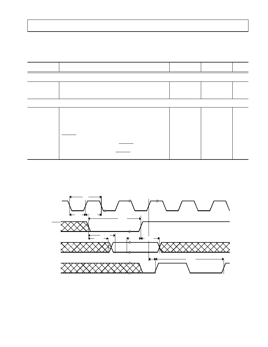
35(/,0,1$5< 7(&+1,&$/ '$7$
This information applies to a product under development. Its characteristics and specifications are subject to change with-
out notice. Analog Devices assumes no obligation regarding future manufacturing unless otherwise agreed to in writing.
25
REV. PrA
For current information contact Analog Devices at 800/262-5643
ADSP-2195
September 2001
Clock In and Clock Out Cycle Timing
Table 8
and
Figure 11
describe clock and reset operations. Per
V
DDINT
Internal (Core) Supply Voltage, 0.3 to 3.0 V on
page 24
, combinations of CLKIN and clock multipliers must not select core/peripheral clocks in excess of 160/100 MHz.
Table 8. Clock In and Clock Out Cycle Timing
Parameter
Description
Min
Max
Unit
Switching Characteristic
t
CKOD
CLKOUT delay from CLKIN
0
5.8
ns
t
CKO
CLKOUT period
1
1
Figure 11
shows a 2 ratio between CLKOUT = 2
CLKIN (or t
HCLK
= 2
t
CCLK
), but the ratio has many programmable options. For more information
see the System Design chapter of the ADSP-219x/2191 DSP Hardware Reference.
10
ns
Timing Requirements
t
CK
CLKIN period
2,3
2
In clock multiplier mode and MSEL60 set for 1:1 (or CLKIN=CCLK), t
CK
=t
CCLK
.
3
In bypass mode, t
CK
=t
CCLK
.
6.25
200
ns
t
CKL
CLKIN low pulse
2.2
ns
t
CKH
CLKIN high pulse
2.2
ns
t
WRST
RESET asserted pulsewidth low
200t
CLKOUT
ns
t
MSLS
MSELx/BYPASS stable before RESET asserted setup
160
µs
t
MSLH
MSELx/BYPASS stable after RESET de-asserted hold
1000
ns
Figure 11. Clock In and Clock Out Cycle Timing
W
& . 2 '
& / . 2 8 7
0 6 ( / ±
% < 3 $ 6 6
' )
5 ( 6 ( 7
& / . , 1
W
: 5 6 7
W
& . +
W
& .
W
& . /
W
0 6 +
W
& . 2
W
3 ) '
W
0 6 '
W
0 6 6
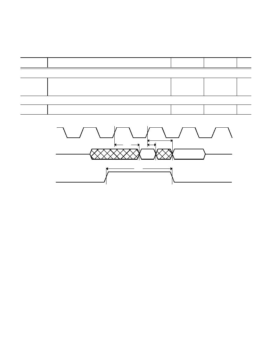
For current information contact Analog Devices at 800/262-5643
ADSP-2195
September 2001
This information applies to a product under development. Its characteristics and specifications are subject to change with-
out notice. Analog Devices assumes no obligation regarding future manufacturing unless otherwise agreed to in writing.
26
REV. PrA
35(/,0,1$5< 7(&+1,&$/ '$7$
Programmable Flags Cycle Timing
Table 9
and
Figure 12
describe programmable flag operations.
Table 9. Programmable Flags Cycle Timing
Parameter
Description
Min
Max
Unit
Switching Characteristic
t
DFO
Flag output delay with respect to HCLK
3
ns
t
HFO
Flag output hold after HCLK high
TBD
TBD
ns
Timing Requirement
t
HFI
Flag input hold is asynchronous
3
ns
Figure 12. Programmable Flags Cycle Timing
F L A G I N P U T
3 )
, 1 3 8 7
W
+ ) ,
3 )
2 8 7 3 8 7
+ & / .
) / $ * 2 8 7 3 8 7
W
' ) 2
W
' ) 2
W
+ ) 2
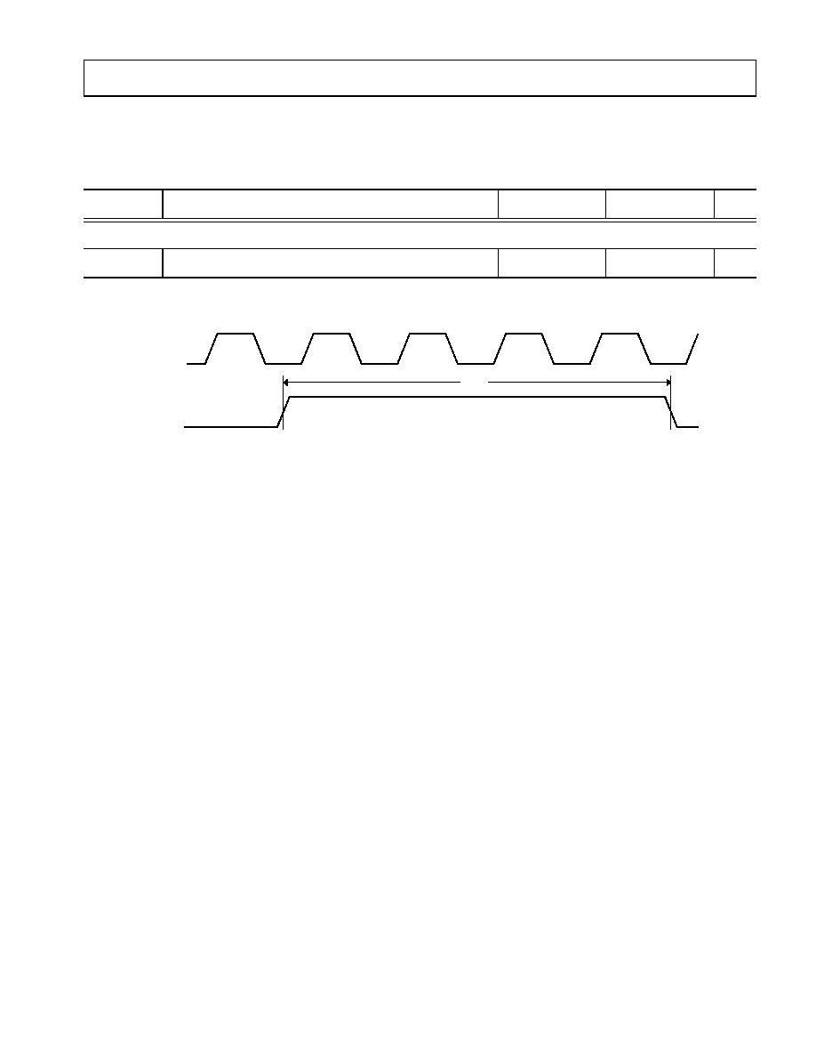
35(/,0,1$5< 7(&+1,&$/ '$7$
This information applies to a product under development. Its characteristics and specifications are subject to change with-
out notice. Analog Devices assumes no obligation regarding future manufacturing unless otherwise agreed to in writing.
27
REV. PrA
For current information contact Analog Devices at 800/262-5643
ADSP-2195
September 2001
Timer PWM_OUT Cycle Timing
Table 10
and
Figure 13
describe timer expired operations. The input signal is asynchronous in "width capture mode" and
has an absolute maximum input frequency of 50 MHz.
Table 10. Timer PWM_OUT Cycle Timing
Parameter
Description
Min
Max
Unit
Switching Characteristic
t
HTO
Timer pulsewidth output
1
1
The minimum time for t
HTO
is one cycle, and the maximum time for t
HTO
equals (2
32
1) cycles.
6.25
(2
32
1) cycles
ns
Figure 13. Timer PWM_OUT Cycle Timing
+ & / .
3 : 0 B 2 8 7
W
+ 7 2
For current information contact Analog Devices at 800/262-5643
ADSP-2195
September 2001
This information applies to a product under development. Its characteristics and specifications are subject to change with-
out notice. Analog Devices assumes no obligation regarding future manufacturing unless otherwise agreed to in writing.
28
REV. PrA
35(/,0,1$5< 7(&+1,&$/ '$7$
External Port Write Cycle Timing
Table 11
and
Figure 14
describe external port write operations.
The external port lets systems extend read/write accesses in three ways: waitstates, ACK input, and combined waitstates
and ACK. To add waits with ACK, the DSP must see ACK low at the rising edge of EMI clock. ACK low causes the DSP
to wait, and the DSP requires two EMI clock cycles after ACK goes high to finish the access. For more information, see
the External Port chapter in the ADSP-219x/2191 DSP Hardware Reference
Table 11. External Port Write Cycle Timing
Parameter
Description
1, 2, 3
1
t
HCLK
is the peripheral clock period.
2
These are preliminary timing parameters that are based on worst-case operating conditions.
3
The pad loads for these timing parameters are 20 pF.
Min
Max
Unit
Switching Characteristics
t
CWA
EMI
4
clock low to WR asserted delay
4
EMI clock is the external port clock that is generated from the EMI clock ratio. This signal is not available on an external pin, but (roughly) corresponds
to HCLK (at similar clock ratios).
2.8
ns
t
CSWS
Chip select asserted to WR de-asserted delay
4.3
6.5
ns
t
AWS
Address valid to WR setup and delay
4.9
7.0
ns
t
AKS
ACK asserted to EMI clock high delay
6.0
ns
t
WSCS
WR de-asserted to chip select de-asserted
4.8
7.0
ns
t
WSA
WR de-asserted to address invalid
4.5
6.6
ns
t
CWD
EMI clock low to WR de-asserted delay
2.5
2.7
ns
t
WW
WR strobe pulsewidth
t
HCLK
0.5
ns
t
CDA
WR to data enable access delay
1.5
4.1
ns
t
CDD
WR to data disable access delay
3.3
7.4
ns
t
DSW
Data valid to WR de-asserted setup
t
HCLK
1.4
t
HCLK
+4.8
ns
t
DHW
WR de-asserted to data invalid hold time; wt_hold=0
3.4
7.4
ns
t
DHW
WR de-asserted to data invalid hold time; wt_hold=1
t
HCLK
+3.4
t
HCLK
+7.4
ns
Timing Requirement
t
AKW
ACK strobe pulsewidth
10.0
ns
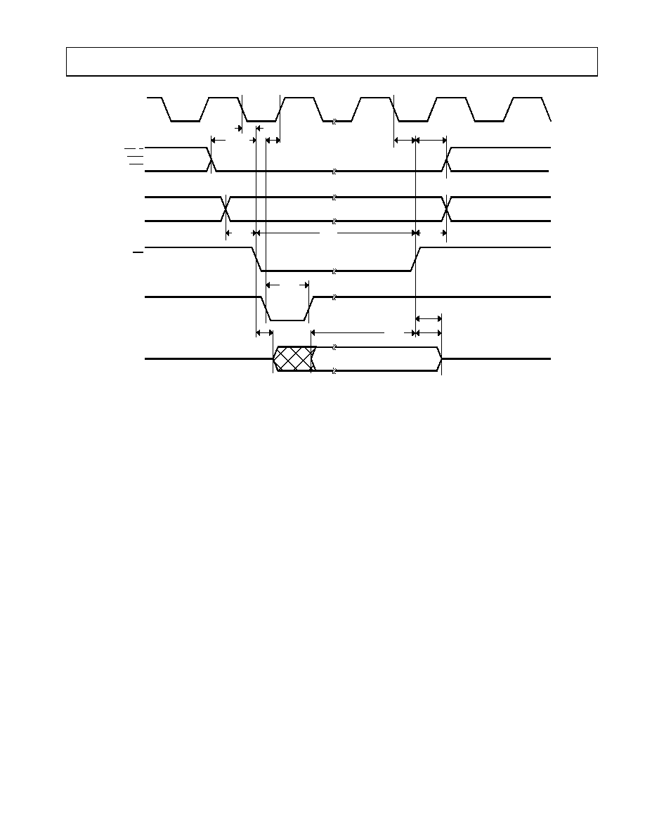
35(/,0,1$5< 7(&+1,&$/ '$7$
This information applies to a product under development. Its characteristics and specifications are subject to change with-
out notice. Analog Devices assumes no obligation regarding future manufacturing unless otherwise agreed to in writing.
29
REV. PrA
For current information contact Analog Devices at 800/262-5643
ADSP-2195
September 2001
Figure 14. External Port Write Cycle Timing
' ±
W
& : $
W
$ : 6
W
& : '
W
: :
W
$ . :
W
' 6 :
W
' + :
W
& ' '
$ & .
: 5
$ ±
0 6 ±
,2 0 6
% 0 6
( 0 ,
& / 2 & .
W
& 6 : 6
W
: 6 $
W
: 6 & 6
W
& ' $
W
$ . 6
For current information contact Analog Devices at 800/262-5643
ADSP-2195
September 2001
This information applies to a product under development. Its characteristics and specifications are subject to change with-
out notice. Analog Devices assumes no obligation regarding future manufacturing unless otherwise agreed to in writing.
30
REV. PrA
35(/,0,1$5< 7(&+1,&$/ '$7$
External Port Read Cycle Timing
Table 12
and
Figure 15
describe external port read operations. For additional information on the ACK signal, see the
discussion on
on page 28
.
Table 12. External Port Read Cycle Timing
Parameter
Description
1, 2, 3
1
t
HCLK
is the peripheral clock period.
2
These are preliminary timing parameters that are based on worst-case operating conditions.
3
The pad loads for these timing parameters are 20 pF.
Min
Max
Unit
Switching Characteristics
t
CRA
EMI
4
clock low to RD asserted delay
4
EMI clock is the external port clock that is generated from the EMI clock ratio. This signal is not available on an external pin, but (roughly) corresponds
to HCLK (at similar clock ratios).
2.8
ns
t
CSRS
Chip select asserted to RD asserted delay
4.3
6.5
ns
t
ARS
Address valid to RD setup and delay
4.9
7.0
ns
t
AKS
ACK asserted to EMI clock high delay
6.0
ns
t
CRD
EMI clock low to RD de-asserted delay
2.5
2.7
ns
t
RSCS
RD de-asserted to chip select de-asserted setup
4.8
7.0
ns
t
RW
RD strobe pulsewidth
t
HCLK
0.5
ns
t
RSA
RD de-asserted to address invalid setup
4.5
6.6
ns
Timing Requirements
t
AKW
ACK strobe pulsewidth
10.0
ns
t
CDA
RD to data enable access delay
0.0
ns
t
RDA
RD asserted to data access setup
t
HCLK
5.5
ns
t
ADA
Address valid to data access setup
t
HCLK
0.2
ns
t
SDA
Chip select asserted to data access setup
t
HCLK
0.6
ns
t
SD
Data valid to RD de-asserted setup
1.8
ns
t
HRD
RD de-asserted to data invalid hold
0.0
ns
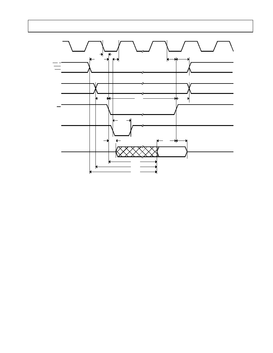
35(/,0,1$5< 7(&+1,&$/ '$7$
This information applies to a product under development. Its characteristics and specifications are subject to change with-
out notice. Analog Devices assumes no obligation regarding future manufacturing unless otherwise agreed to in writing.
31
REV. PrA
For current information contact Analog Devices at 800/262-5643
ADSP-2195
September 2001
Figure 15. External Port Read Cycle Timing
' ±
W
& 5 $
W
$ 5 6
W
& 5 '
W
5 :
W
$ . :
W
& ' $
W
5 ' $
W
$ ' $
W
6 ' $
W
6 '
W
+ 5 '
$ & .
5 '
$ ±
0 6 ±
,2 0 6
% 0 6
( 0 ,
& / 2 & .
W
& 6 5 6
W
5 6 $
W
5 6 & 6
W
$ . 6

For current information contact Analog Devices at 800/262-5643
ADSP-2195
September 2001
This information applies to a product under development. Its characteristics and specifications are subject to change with-
out notice. Analog Devices assumes no obligation regarding future manufacturing unless otherwise agreed to in writing.
32
REV. PrA
35(/,0,1$5< 7(&+1,&$/ '$7$
External Port Bus Request and Grant Cycle Timing
Table 13
and
Figure 16
describe external port bus request and bus grant operations.
Table 13. External Port Bus Request and Grant Cycle Timing
Parameter
Description
1, 2, 3
1
t
HCLK
is the peripheral clock period.
2
These are preliminary timing parameters that are based on worst-case operating conditions.
3
The pad loads for these timing parameters are 20 pF.
Min
Max
Unit
Switching Characteristics
t
SD
CLKOUT high to xMS, address, and RD/WR disable
4.3
ns
t
SE
CLKOUT low to xMS, address, and RD/WR enable
4.0
ns
t
DBG
CLKOUT high to BG asserted setup
2.2
ns
t
EBG
CLKOUT high to BG de-asserted hold time
2.2
ns
t
DBH
CLKOUT high to BGH asserted setup
2.4
ns
t
EBH
CLKOUT high to BGH de-asserted hold time
2.4
ns
Timing Requirements
t
BS
BR asserted to CLKOUT high setup
4.6
ns
t
BH
CLKOUT high to BR de-asserted hold time
0.0
ns
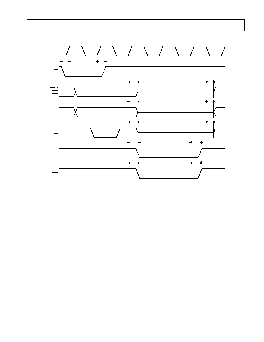
35(/,0,1$5< 7(&+1,&$/ '$7$
This information applies to a product under development. Its characteristics and specifications are subject to change with-
out notice. Analog Devices assumes no obligation regarding future manufacturing unless otherwise agreed to in writing.
33
REV. PrA
For current information contact Analog Devices at 800/262-5643
ADSP-2195
September 2001
Figure 16. External Port Bus Request and Grant Cycle Timing
W
% +
% 5
$ ±
0 6 ±
,2 0 6
% 0 6
& / . 2 8 7
W
% 6
W
6 '
W
6 '
W
6 '
W
' % *
W
' % +
W
6 (
W
6 (
W
6 (
W
( % *
W
( % +
% *
: 5
5 '
% * +
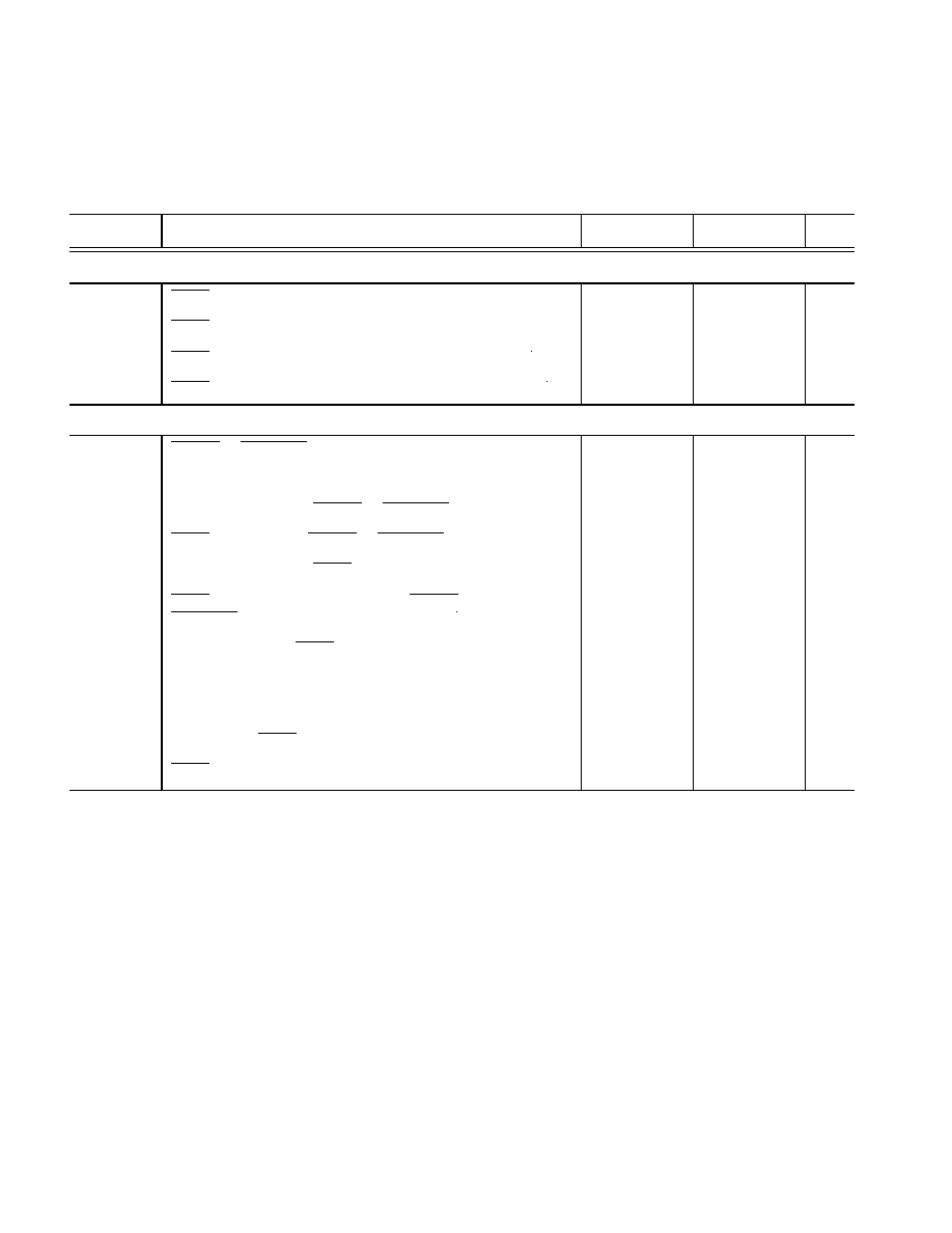
For current information contact Analog Devices at 800/262-5643
ADSP-2195
September 2001
This information applies to a product under development. Its characteristics and specifications are subject to change with-
out notice. Analog Devices assumes no obligation regarding future manufacturing unless otherwise agreed to in writing.
34
REV. PrA
35(/,0,1$5< 7(&+1,&$/ '$7$
Host Port ALE Mode Write Cycle Timing
Table 14
and
Figure 17
describe host port write operations in Address Latch Enable (ALE) mode. For more information
on ACK, Ready, ALE, and ACC mode selection, see the Host port modes description
on page 10
.
Table 14. Host Port ALE Mode Write Cycle Timing
Parameter
Description
Min
Max
Unit
Switching Characteristics
t
WHKS
HWR asserted to HACK asserted (setup, ACK Mode)
0.6
0.6+t
NH
1
1
t
NH
are peripheral bus latencies (n t
HCLK
); these are internal DSP latencies related to the number of peripherals attempting to access DSP memory at
the same time.
ns
t
WHKH
HWR de-asserted to HACK de-asserted (hold, ACK Mode)
2
ns
t
WHS
HWR asserted to HACK asserted (setup, Ready Mode)
0.6
ns
t
WHH
HWR asserted to HACK de-asserted (hold, Ready Mode)
2+t
NH
1
ns
Timing Requirements
t
CSAL
HCMS or HCIOMS asserted to HALE asserted
0
ns
t
ALPW
HALE asserted pulsewidth
4
ns
t
ALCSW
HALE de-asserted to HCMS or HCIOMS de-asserted
1
ns
t
WCSW
HWR de-asserted to HCMS or HCIOMS de-asserted
1
ns
t
ALW
HALE de-asserted to HWR asserted
1
ns
t
WCS
HWR de-asserted (after last byte) to HCMS or
HCIOMS de-asserted (ready for next write)
1
ns
t
HKWD
HACK asserted to HWR de-asserted (hold, ACK Mode)
1.5
ns
t
AALS
Address valid to HALE de-asserted (setup)
4
ns
t
ALAH
HALE de-asserted to address invalid (hold)
1.5
ns
t
DWS
Data valid to HWR de-asserted (setup)
4
ns
t
WDH
HWR de-asserted to data invalid (hold)
1
ns
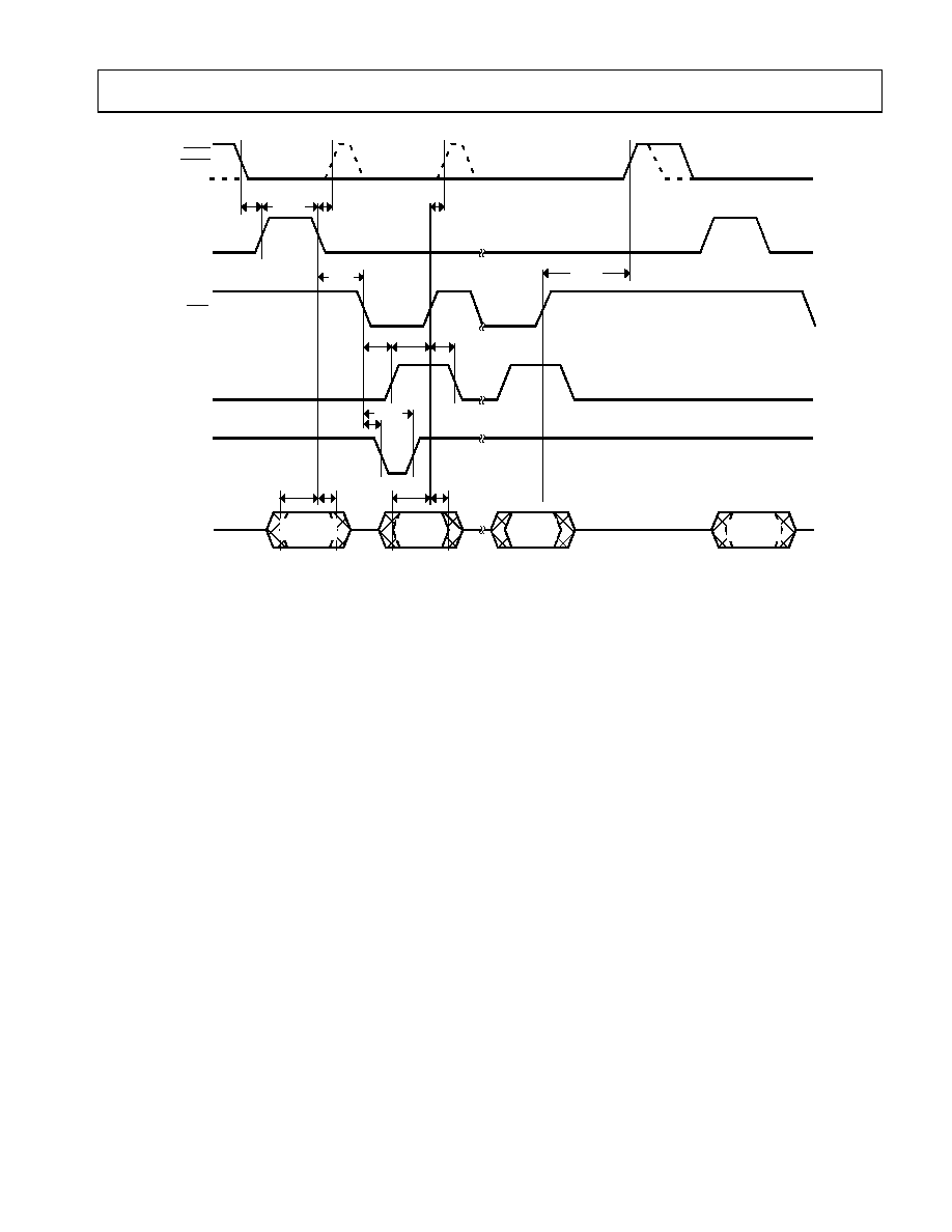
35(/,0,1$5< 7(&+1,&$/ '$7$
This information applies to a product under development. Its characteristics and specifications are subject to change with-
out notice. Analog Devices assumes no obligation regarding future manufacturing unless otherwise agreed to in writing.
35
REV. PrA
For current information contact Analog Devices at 800/262-5643
ADSP-2195
September 2001
Figure 17. Host Port ALE Mode Write Cycle Timing
W
$ / $ +
$ ' ' 5 ( 6 6
9 $ / ,'
' $ 7 $
9 $ / ,'
' $ 7 $
9 $ / ,'
$ ' ' 5 ( 6 6
9 $ / ,'
/ $ 6 7
% < 7 (
) , 5 6 7
% < 7 (
6 7 $ 5 7
1 ( ; 7 : 2 5 '
6 7 $ 5 7
) , 5 6 7 : 2 5 '
+ $ ' ±
+ $
W
: ' +
W
$ $ / 6
W
' : 6
W
& 6 $ /
W
: + . 6
W
: & 6
+ : 5
+ $ / (
+ & 0 6
+ , 2 0 6
+ $ & .
$ & .
0 2 ' (
W
: + . +
+ $ & . ( $ & + % < 7 (
+ $ & . ) ,5 6 7 % < 7 (
+ $ & .
5 ( $ ' <
0 2 ' (
W
$ / 3 :
W
$ / & 6 :
W
$ / :
W
+ . : '
W
: & 6 :
W
: + 6
W
: + +
For current information contact Analog Devices at 800/262-5643
ADSP-2195
September 2001
This information applies to a product under development. Its characteristics and specifications are subject to change with-
out notice. Analog Devices assumes no obligation regarding future manufacturing unless otherwise agreed to in writing.
36
REV. PrA
35(/,0,1$5< 7(&+1,&$/ '$7$
Host Port ACC Mode Write Cycle Timing
Table 15
and
Figure 18
describe host port write operations in Address Cycle Control (ACC) mode. For more information
on ACK, Ready, ALE, and ACC mode selection, see the Host port modes description
on page 10
.
Table 15. Host Port ACC Mode Write Cycle Timing
Parameter
Description
Min
Max
Unit
Switching Characteristics
t
WHKS
HWR asserted to HACK asserted (setup, ACK Mode)
0.6
0.6+t
NH
1
1
t
NH
are peripheral bus latencies (n
t
HCLK
); these are internal DSP latencies related to the number of peripherals attempting to access DSP memory at
the same time.
ns
t
WHKH
HWR de-asserted to HACK de-asserted (hold, ACK Mode)
2
ns
t
WHS
HWR asserted to HACK asserted (setup, Ready Mode)
0.6
ns
t
WHH
HWR asserted to HACK de-asserted (hold, Ready Mode)
2+t
NH
1
ns
Timing Requirements
t
WAL
HWR asserted to HALE de-asserted (delay)
1.5
ns
t
CSAL
HCMS or HCIOMS asserted to HALE asserted (delay)
0
ns
t
ALCS
HALE de-asserted to optional HCMS or HCIOMS
de-asserted
1
ns
t
WCSW
HWR de-asserted to HCMS or HCIOMS de-asserted
1
ns
t
ALW
HALE asserted to HWR asserted
0.5
ns
t
CSW
HCMS or HCIOMS asserted to HWR asserted
1
2
ns
t
WCS
HWR de-asserted (after last byte) to HCMS or
HCIOMS de-asserted (ready for next write)
1
ns
t
ALEW
HALE de-asserted to HWR asserted
1
ns
t
HKWD
HACK asserted to HWR de-asserted (hold, ACK Mode)
1.5
ns
t
ADW
Address valid to HWR asserted (setup)
4
ns
t
WAD
HWR de-asserted to address invalid (hold)
1
ns
t
DWS
Data valid to HWR de-asserted (setup)
4
ns
t
WDH
HWR de-asserted to data invalid (hold)
1
ns
35(/,0,1$5< 7(&+1,&$/ '$7$
This information applies to a product under development. Its characteristics and specifications are subject to change with-
out notice. Analog Devices assumes no obligation regarding future manufacturing unless otherwise agreed to in writing.
37
REV. PrA
For current information contact Analog Devices at 800/262-5643
ADSP-2195
September 2001
Figure 18. Host Port ACC Mode Write Cycle Timing
+ $ & . ) ,5 6 7 % < 7 (
W
: ' +
+ $ ' ±
+ $
W
: $ '
$ ' ' 5 ( 6 6
9 $ / ,'
' $ 7 $
9 $ / ,'
' $ 7 $
9 $ / ,'
$ ' ' 5 ( 6 6
9 $ / ,'
/ $ 6 7
% < 7 (
) , 5 6 7
% < 7 (
6 7 $ 5 7
1 ( ; 7 : 2 5 '
6 7 $ 5 7
) , 5 6 7 : 2 5 '
W
$ ' :
W
' : 6
W
: + . +
W
: + . 6
W
& 6 $ /
W
: & 6
+ : 5
+ $ / (
+ & 0 6
+ , 2 0 6
W
$ / ( :
+ $ & .
$ & .
0 2 ' (
W
+ . : '
+ $ & . ( $ & + % < 7 (
+ $ & .
5 ( $ ' <
0 2 ' (
W
: $ /
W
$ / & 6
W
$ / :
W
& 6 :
W
: & 6 :
W
: + 6
W
: + +

For current information contact Analog Devices at 800/262-5643
ADSP-2195
September 2001
This information applies to a product under development. Its characteristics and specifications are subject to change with-
out notice. Analog Devices assumes no obligation regarding future manufacturing unless otherwise agreed to in writing.
38
REV. PrA
35(/,0,1$5< 7(&+1,&$/ '$7$
Host Port ALE Mode Read Cycle Timing
Table 16
and
Figure 19
describe host port read operations in Address Latch Enable (ALE) mode. For more information
on ACK, Ready, ALE, and ACC mode selection, see the Host port modes description
on page 10
.
Table 16. Host Port ALE Mode Read Cycle Timing
Parameter
Description
Min
Max
Unit
Switching Characteristics
t
RHKS
HRD asserted to HACK asserted (setup, ACK Mode)
2
2+t
NH
1
1
t
NH
are peripheral bus latencies (n
t
HCLK
); these are internal DSP latencies related to the number of peripherals attempting to access DSP memory at
the same time.
ns
t
RHKH
HRD de-asserted to HACK de-asserted (hold, ACK Mode)
2
ns
t
RHS
HRD asserted to HACK asserted (setup, Ready Mode)
2
ns
t
RHH
HRD asserted to HACK de-asserted (hold, Ready Mode)
2+t
NH
1
ns
Timing Requirements
t
CSAL
HCMS or HCIOMS asserted to HALE asserted (delay)
0
ns
t
ALCS
HALE de-asserted to optional HCMS or HCIOMS
de-asserted
1
ns
t
RCSW
HRD de-asserted to HCMS or HCIOMS de-asserted
1
ns
t
ALR
HALE de-asserted to HRD asserted
1
ns
t
RCS
HRD de-asserted (after last byte) to HCMS or
HCIOMS de-asserted (ready for next read)
1
ns
t
ALPW
HALE asserted pulsewidth
4
ns
t
HKRD
HACK asserted to HRD de-asserted (hold, ACK Mode)
1.5
ns
t
AALS
Address valid to HALE de-asserted (setup)
4
ns
t
ALAH
HALE de-asserted to address invalid (hold)
1
ns
t
RDH
HRD de-asserted to data invalid (hold)
1
ns
35(/,0,1$5< 7(&+1,&$/ '$7$
This information applies to a product under development. Its characteristics and specifications are subject to change with-
out notice. Analog Devices assumes no obligation regarding future manufacturing unless otherwise agreed to in writing.
39
REV. PrA
For current information contact Analog Devices at 800/262-5643
ADSP-2195
September 2001
Figure 19. Host Port ALE Mode Read Cycle TIming
+ $ ' ±
+ $
W
$ / $ +
$ ' ' 5 ( 6 6
9 $ / ,'
' $ 7 $
9 $ / ,'
' $ 7 $
9 $ / ,'
$ ' ' 5 ( 6 6
9 $ / , '
/ $ 6 7
% < 7 (
) , 5 6 7
% < 7 (
6 7 $ 5 7
1 ( ; 7 : 2 5 '
6 7 $ 5 7
) , 5 6 7
: 2 5 '
W
5 ' +
W
$ $ / 6
W
& 6 $ /
W
5 & 6
+ 5 '
+ $ / (
+ & 0 6
+ , 2 0 6
+ $ & .
$ & .
0 2 ' (
W
5 + . +
+ $ & .
5 ( $ ' <
0 2 ' (
+ $ & . ) 2 5 ( $ & + % < 7 (
W
$ / 3 :
W
$ / & 6
W
+ . 5 '
W
$ / 5
W
5 & 6 :
+ $ & . ) ,5 6 7 % < 7 (
+ $ & .
5 ( $ ' <
0 2 ' (
W
5 + 6
W
5 + +
W
5 + . 6
For current information contact Analog Devices at 800/262-5643
ADSP-2195
September 2001
This information applies to a product under development. Its characteristics and specifications are subject to change with-
out notice. Analog Devices assumes no obligation regarding future manufacturing unless otherwise agreed to in writing.
40
REV. PrA
35(/,0,1$5< 7(&+1,&$/ '$7$
Host Port ACC Mode Read Cycle Timing
Table 17
and
Figure 20
describe host port read operations in Address Cycle Control (ACC) mode. For more information
on ACK, Ready, ALE, and ACC mode selection, see the Host port modes description
on page 10
.
Table 17. Host Port ACC Mode Read Cycle Timing
Parameter
Description
Min
Max
Unit
Switching Characteristics
t
RHKS
HRD asserted to HACK asserted (setup, ACK Mode)
1
1+t
NH
1
1
t
NH
are peripheral bus latencies (n
t
HCLK
); these are internal DSP latencies related to the number of peripherals attempting to access DSP memory at
the same time.
ns
t
RHKH
HRD de-asserted to HACK de-asserted (hold, ACK Mode)
2
ns
t
RHS
HRD asserted to HACK asserted (setup, Ready Mode)
1
ns
t
RHH
HRD asserted to HACK de-asserted (hold, Ready Mode)
2+t
NH
1
ns
Timing Requirements
t
CSAL
HCMS or HCIOMS asserted to HALE asserted (delay)
0
ns
t
ALCS
HALE de-asserted to optional HCMS or HCIOMS
de-asserted
1
ns
t
RCSW
HRD de-asserted to HCMS or HCIOMS de-asserted
1
ns
t
ALW
HALE asserted to HWR asserted
0.5
ns
t
ALER
HALE de-asserted to HWR asserted
1
ns
t
CSR
HCMS or HCIOMS asserted to HRD asserted
1
2
ns
t
RCS
HRD de-asserted (after last byte) to HCMS or
HCIOMS de-asserted (ready for next read)
1
ns
t
WAL
HWR de-asserted to HALE de-asserted (delay)
1.5
ns
t
HKRD
HACK asserted to HRD de-asserted (hold, ACK Mode)
1.5
ns
t
ADW
Address valid to HWR de-asserted (setup)
4
ns
t
WAD
HWR de-asserted to address invalid (hold)
1
ns
t
RDH
HRD de-asserted to data invalid (hold)
1
ns
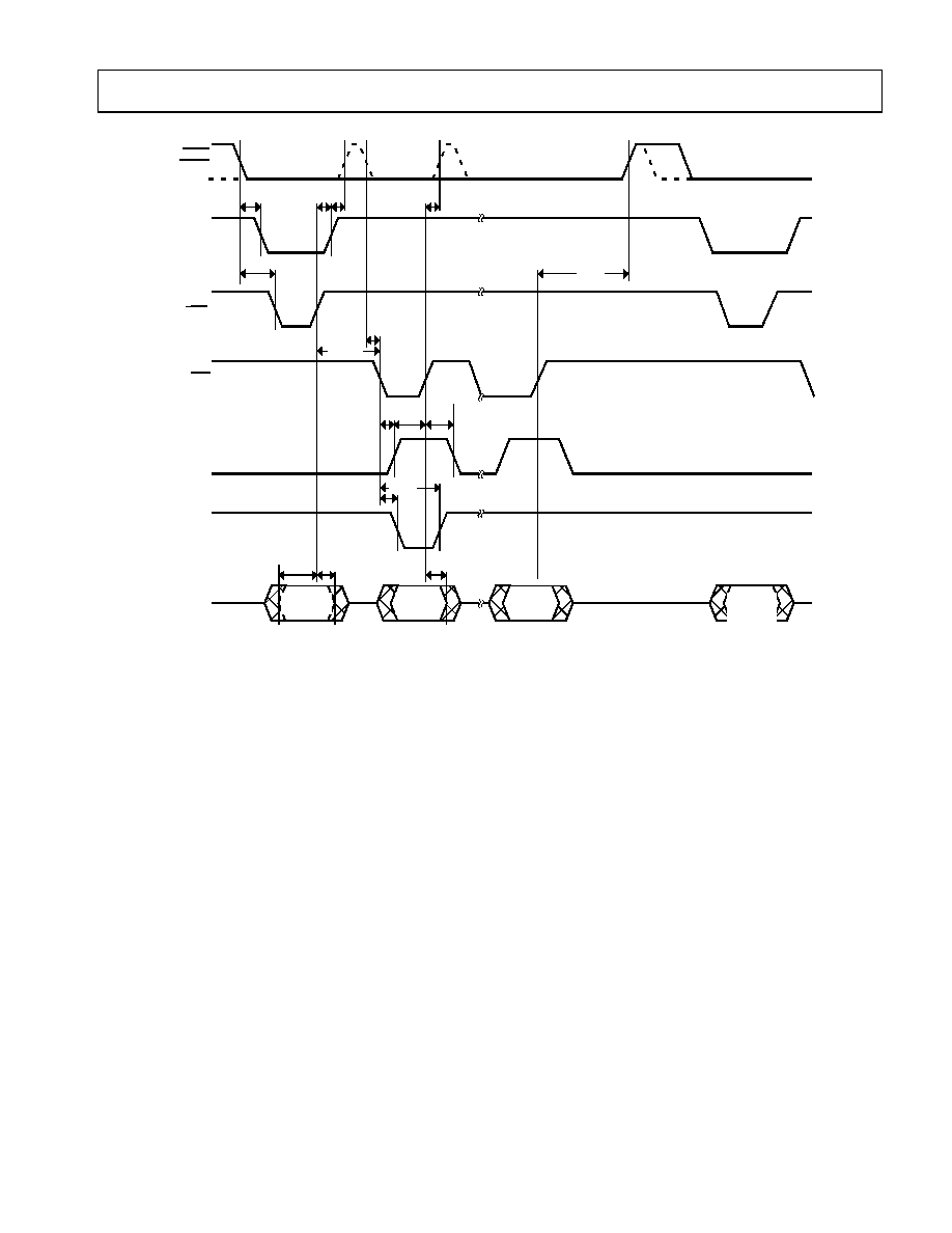
35(/,0,1$5< 7(&+1,&$/ '$7$
This information applies to a product under development. Its characteristics and specifications are subject to change with-
out notice. Analog Devices assumes no obligation regarding future manufacturing unless otherwise agreed to in writing.
41
REV. PrA
For current information contact Analog Devices at 800/262-5643
ADSP-2195
September 2001
Figure 20. Host Port ACC Mode Read Cycle TIming
W
5 ' +
+ $ ' ±
+ $
W
: $ '
W
$ ' :
$ ' ' 5 ( 6 6
9 $ / ,'
' $ 7 $
9 $ / ,'
' $ 7 $
9 $ / ,'
$ ' ' 5 ( 6
6
9 $ / , '
/ $ 6 7
% < 7 (
) , 5 6 7
% < 7 (
6 7 $ 5 7
1 ( ; 7 : 2 5 '
6 7 $ 5 7
) , 5 6 7 : 2 5 '
W
5 + . +
W
+ . 5 '
W
& 6 $ /
W
5 + . 6
W
5 & 6
+ : 5
+ $ / (
+ & 0 6
+ , 2 0 6
W
$ / :
+ $ & .
$ & .
0 2 ' (
+ $ & . ( $ & + % < 7 (
+ 5 '
W
: $ /
W
$ / & 6
W
& 6 5
W
$ / ( 5
W
5 & 6 :
+ $ & .
5 ( $ ' <
0 2 ' (
+ $ & . ) ,5 6 7 % < 7 (
+ $ & .
5 ( $ ' <
0 2 ' (
W
5 + 6
W
5 + +

For current information contact Analog Devices at 800/262-5643
ADSP-2195
September 2001
This information applies to a product under development. Its characteristics and specifications are subject to change with-
out notice. Analog Devices assumes no obligation regarding future manufacturing unless otherwise agreed to in writing.
42
REV. PrA
35(/,0,1$5< 7(&+1,&$/ '$7$
Serial Port (SPORT) Clocks and Data Timing
Table 18
and
Figure 21
describe SPORT transmit and receive operations.
Table 18. Serial Port (SPORT) Clocks and Data Timing
1
1
To determine whether communication is possible between two devices at clock speed n, the following specifications must be confirmed:
1) frame sync delay and frame sync setup and hold, 2) data delay and data setup and hold, and 3) SCLK width.
Parameter
Description
Min
Max
Unit
Switching Characteristics
t
HOFSE
RFS Hold after RCLK (Internally Generated RFS)
2
2
Referenced to drive edge.
0
12.4
ns
t
DFSE
RFS Delay after RCLK (Internally Generated RFS)
2
0
12.4
ns
t
DDTEN
Transmit Data Delay after TCLK
2
0
12.1
ns
t
DDTTE
Data Disable from External TCLK
2
0
12.0
ns
t
DDTIN
Data Enable from Internal TCLK
2
0
6.8
ns
t
DDTTI
Data Disable from Internal TCLK
2
0
6.3
ns
Timing Requirements
t
SCLKIW
TCLK/RCLK Width
20
ns
t
SFSI
TFS/RFS Setup before TCLK/RCLK
3
3
Referenced to sample edge.
0.6
ns
t
HFSI
TFS/RFS Hold after TCLK/RCLK
3, 4
4
RFS hold after RCLK when MCE = 1, MFD = 0 is 0 ns minimum from drive edge. TFS hold after TCLK for late external TFS is 0 ns minimum from
drive edge.
0.3
ns
t
SDRI
Receive Data Setup before RCLK
3
2.3
ns
t
HDRI
Receive Data Hold after RCLK
3
1.9
ns
t
SCLKW
TCLK/RCLK Width
20
ns
t
SFSE
TFS/RFS Setup before TCLK/RCLK
3
0.6
ns
t
HFSE
TFS/RFS Hold after TCLK/RCLK
3, 4
0.6
ns
t
SDRE
Receive Data Setup before RCLK
3
2.2
ns
t
HDRE
Receive Data Hold after RCLK
3
1.8
ns
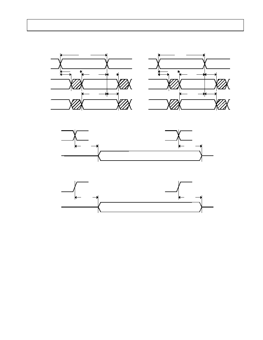
35(/,0,1$5< 7(&+1,&$/ '$7$
This information applies to a product under development. Its characteristics and specifications are subject to change with-
out notice. Analog Devices assumes no obligation regarding future manufacturing unless otherwise agreed to in writing.
43
REV. PrA
For current information contact Analog Devices at 800/262-5643
ADSP-2195
September 2001
Figure 21. Serial Port (SPORT) Clocks and Data
W
+ ) 6 (
W
+ ' 5 (
W
+ ' 5 ,
' 5 ,9 ( ( ' * (
' 5 ,9 ( ( ' * (
7 & / .
W
' ' 7 ( 1
W
' ' 7 7 (
7 & / . , 1 7
7 & / . ( ; 7
5 7 & / .
) 6
' 5 , 9 (
( ' * (
6 $ 0 3 / (
( ' * (
' $ 7 $ 7 5 $ 1 6 ) ( 5 ² ( ; 7 ( 5 1 $ / & / 2 & .
' 5
W
6 & / . :
W
' ) 6 (
W
+ 2 ) 6 (
W
6 ) 6 (
W
6 ' 5 (
1 2 7 ( ( , 7 + ( 5 7 + ( 5 , 6 , 1 * ( ' * ( 2 5 ) $ / / ,1 * ( ' * ( 2 ) 5 & / . ( ; 7 ( 5 1 $ /
2 5 5 & / . ,1 7 ( 5 1 $ / & $ 1 % ( 8 6 ( ' $ 6 7 + ( $ & 7 , 9 ( 6 $ 0 3 / , 1 * ( ' * (
' 7
' 7
5 7 & / .
) 6
' 5 , 9 (
( ' * (
6 $ 0 3 / (
( ' * (
' $ 7 $ 7 5 $ 1 6 ) ( 5 ² , 1 7 ( 5 1 $ / & / 2 & .
' 5
W
6 & / . , :
W
' ) 6 (
W
+ 2 ) 6 (
W
6 ) 6 ,
W
+ ) 6 ,
W
6 ' 5 ,
7 & / .
W
' ' 7 , 1
W
' ' 7 7 ,
' 5 ,9 ( ( ' * (
' 5 ,9 ( ( ' * (

For current information contact Analog Devices at 800/262-5643
ADSP-2195
September 2001
This information applies to a product under development. Its characteristics and specifications are subject to change with-
out notice. Analog Devices assumes no obligation regarding future manufacturing unless otherwise agreed to in writing.
44
REV. PrA
35(/,0,1$5< 7(&+1,&$/ '$7$
Serial Port (SPORT) Frame Synch Timing
Table 19
and
Figure 22
describe SPORT frame synch operations.
To determine whether communication is possible between two devices at clock speed n, the following specifications must
be confirmed: 1) frame sync delay and frame sync setup and hold, 2) data delay and data setup and hold, and 3)
R/TCLK width.
Table 19. Serial Port (SPORT) Frame Synch Timing
Parameter
Description
Min
Max
Unit
Switching Characteristics
t
HOFSE
RFS Hold after RCLK (Internally Generated RFS)
1
1
Referenced to drive edge.
12.4
ns
t
HOFSI
TFS Hold after TCLK (Internally Generated TFS)
1
12.2
ns
t
DDTENFS
Data Enable from late FS or MCE = 1, MFD = 0
2
2
MCE = 1, TFS enable and TFS valid follow t
DDTLFSE
and t
DDTENFS
.
4.7
ns
t
DDTLFSE
Data Delay from Late External TFS or External RFS with
MCE = 1, MFD = 0
3
4.7
ns
t
HDTE
Transmit Data Hold after TCLK (external clk)
1
12.4
ns
t
HDTI
Transmit Data Hold after TCLK (internal clk)
1
0
12.2
ns
t
DDTE
Transmit Data Delay after TCLK (external clk)
1
0
12.2
ns
t
DDTI
Transmit Data Delay after TCLK (internal clk)
1
0
11.1
ns
Timing Requirements
t
SFSE
TFS/RFS Setup before TCLK/RCLK (external clk)
3
3
Referenced to sample edge.
0.6
TBD
ns
t
SFSI
TFS/RFS Setup before TCLK/RCLK (internal clk)
3
0.6
TBD
ns
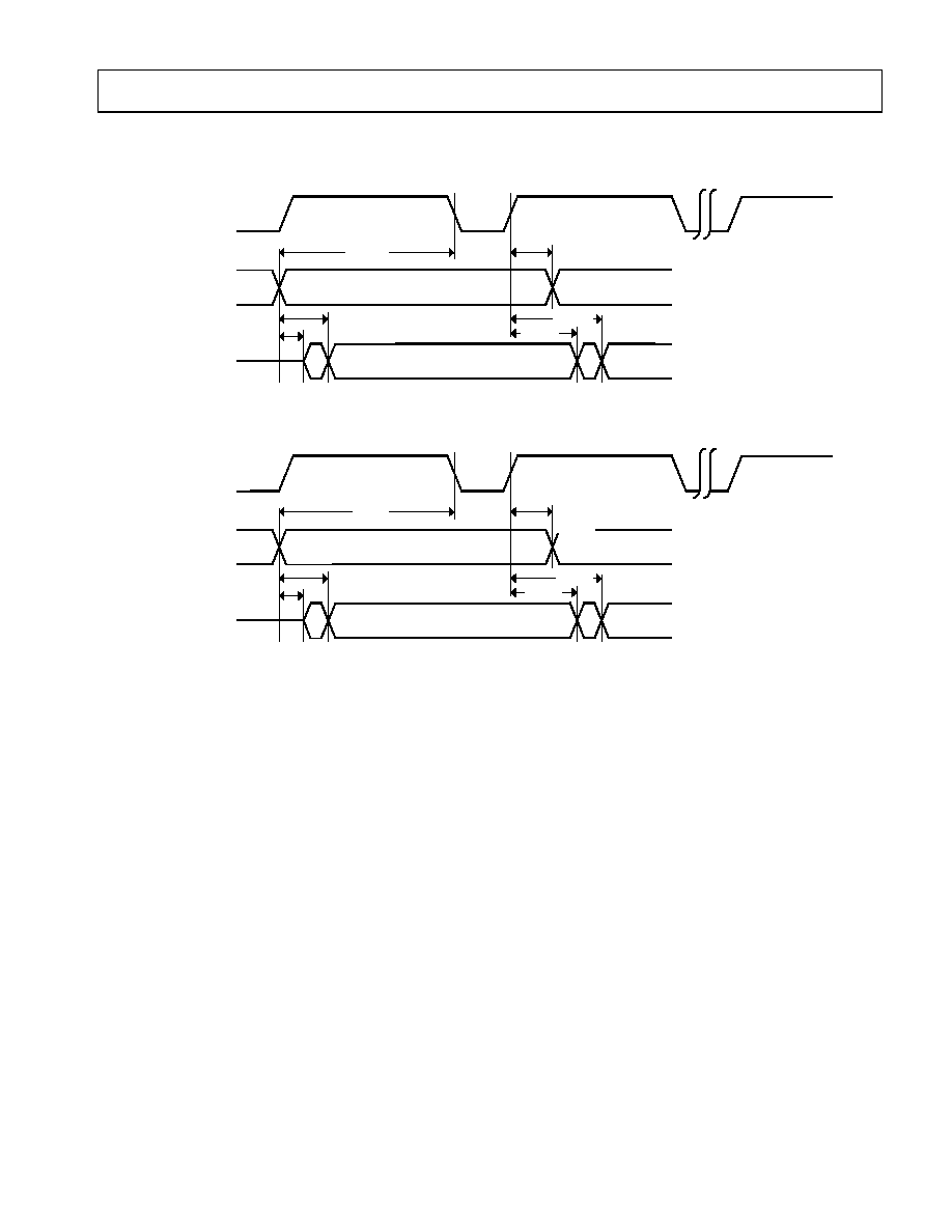
35(/,0,1$5< 7(&+1,&$/ '$7$
This information applies to a product under development. Its characteristics and specifications are subject to change with-
out notice. Analog Devices assumes no obligation regarding future manufacturing unless otherwise agreed to in writing.
45
REV. PrA
For current information contact Analog Devices at 800/262-5643
ADSP-2195
September 2001
Figure 22. Serial Port (SPORT) Frame Synch
6 ( ( 1 2 7 (
' 5 , 9 (
6 $ 0 3 / (
' 5 , 9 (
) , 5 6 7 % , 7
6 ( & 2 1 ' % , 7
5 7 & / .
) 6
W
+ 2 ) 6 ( ,
W
' ' 7 ( 1 ) 6
W
' ' 7 / ) 6 (
' 5
W
6 ) 6 ( ,
/$ 7 ( ( ; 7 ( 5 1 $ / 7 5 $ 1 6 0 ,7 ) 6
(; 7( 5 1 $ / 5 ( & ( ,9 ( )6 : ,7 + 0 & ( 0 )'
6 ( ( 1 2 7 (
' 5 , 9 (
6 $ 0 3 / (
' 5 , 9 (
) , 5 6 7 % , 7
6 ( & 2 1 ' % , 7
5 7 & / .
) 6
W
+ 2 ) 6 (
,
W
' ' 7 ( 1 ) 6
W
' ' 7 / ) 6 (
' 7
W
6 ) 6 ( ,
W
' ' 7 ( ,
W
+ ' 7 ( ,
W
' ' 7 ( ,
W
+ ' 7 ( ,
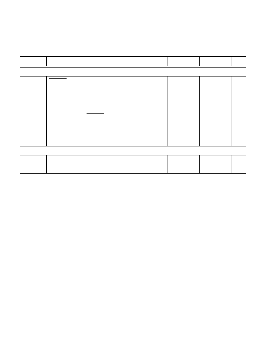
For current information contact Analog Devices at 800/262-5643
ADSP-2195
September 2001
This information applies to a product under development. Its characteristics and specifications are subject to change with-
out notice. Analog Devices assumes no obligation regarding future manufacturing unless otherwise agreed to in writing.
46
REV. PrA
35(/,0,1$5< 7(&+1,&$/ '$7$
Serial Peripheral Interface (SPI) Port--Master Timing
Table 20
and
Figure 23
describe SPI port master operations.
Table 20. Serial Peripheral Interface (SPI) Port--Master Timing
Parameter
Description
Min
Max
Unit
Switching Characteristics
t
SDSCIM
SPIxSEL low to first SCLK edge (x=0 or 1)
2t
HCLK
ns
t
SPICHM
Serial clock high period
2t
HCLK
ns
t
SPICLM
Serial clock low period
2t
HCLK
ns
t
SPICLK
Serial clock period
4t
HCLK
ns
t
HDSM
Last SCLK edge to SPIxSEL high (x=0 or 1)
2t
HCLK
ns
t
SPITDM
Sequential transfer delay
2t
HCLK
ns
t
DDSPID
SCLK edge to data out valid (data out delay)
0
6
ns
t
HDSPID
SCLK edge to data out invalid (data out hold)
0
5
ns
Timing Requirements
t
SSPID
Data input valid to SCLK edge (data input setup)
1.6
ns
t
HSPID
SCLK sampling edge to data input invalid
1.6
ns
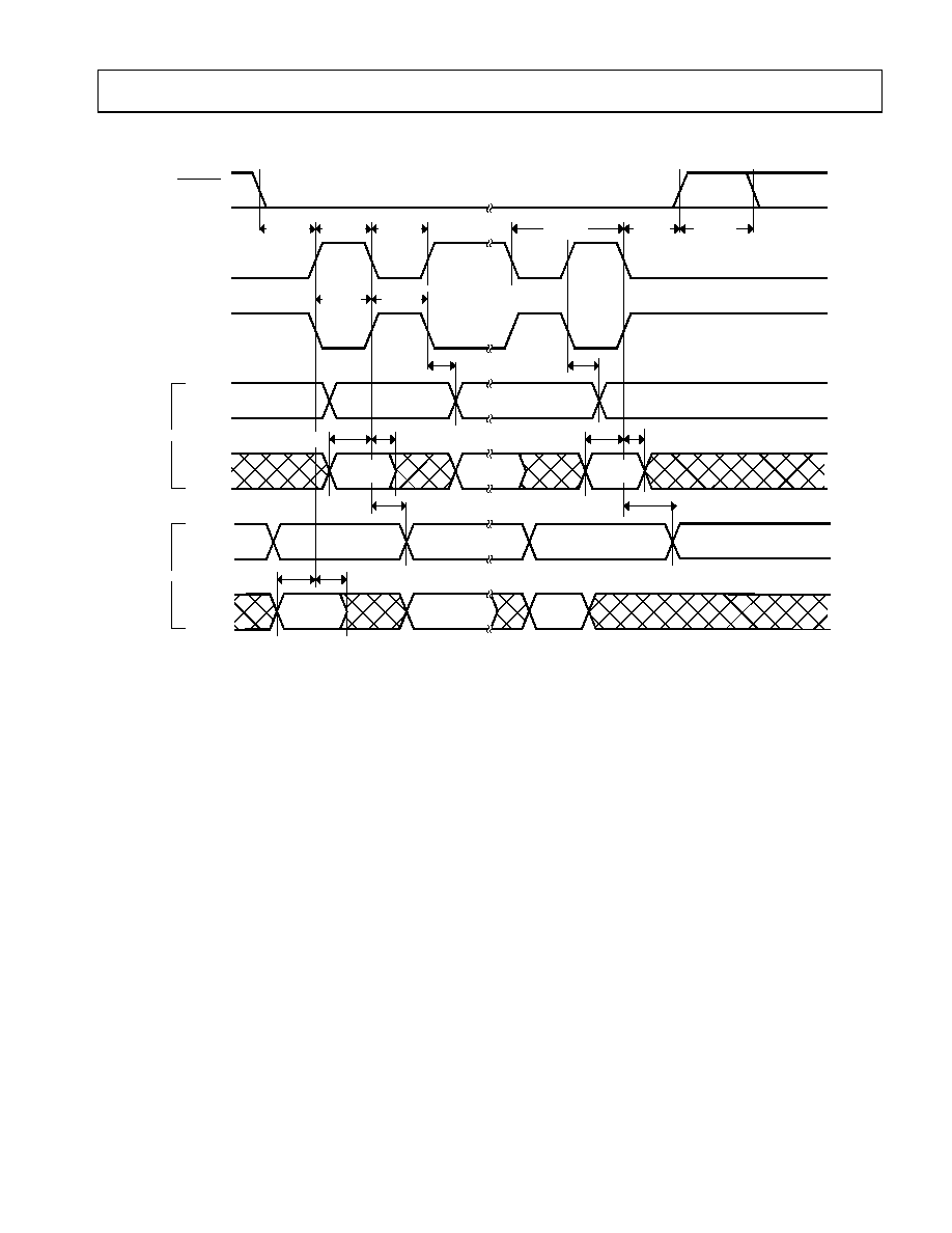
35(/,0,1$5< 7(&+1,&$/ '$7$
This information applies to a product under development. Its characteristics and specifications are subject to change with-
out notice. Analog Devices assumes no obligation regarding future manufacturing unless otherwise agreed to in writing.
47
REV. PrA
For current information contact Analog Devices at 800/262-5643
ADSP-2195
September 2001
Figure 23. Serial Peripheral Interface (SPI) Port--Master
W
6 6 3 , '
W
+ 6 3 , '
W
+ ' 6 3 , '
/ 6 %
0 6 %
W
+ 6 3 , '
W
' ' 6 3 , '
0 2 6 ,
2 8 7 3 8 7
0 ,6 2
, 1 3 8 7
6 3 , [ 6 ( /
2 8 7 3 8 7
[ R U
6 & / .
& 3 2 /
2 8 7 3 8 7
6 & / .
& 3 2 /
2 8 7 3 8 7
W
6 3 , & + 0
W
6 3 , & / 0
W
6 3 , & / 0
W
6 3 , & / .
W
6 3 , & + 0
W
+ ' 6 0
W
6 3 , 7 ' 0
W
+ ' 6 3 , '
/ 6 %
9 $ / , '
/ 6 %
0 6 %
0 6 %
9 $ / ,'
W
+ 6 3 , '
W
' ' 6 3 , '
0 2 6 ,
2 8 7 3 8 7
0 , 6 2
, 1 3 8 7
W
6 6 3 , '
&3+$
&3+$
0 6 %
9 $ / ,'
W
6 ' 6 & , 0
W
6 6 3 , '
/ 6 %
9 $ / , '
For current information contact Analog Devices at 800/262-5643
ADSP-2195
September 2001
This information applies to a product under development. Its characteristics and specifications are subject to change with-
out notice. Analog Devices assumes no obligation regarding future manufacturing unless otherwise agreed to in writing.
48
REV. PrA
35(/,0,1$5< 7(&+1,&$/ '$7$
Serial Peripheral Interface (SPI) Port--Slave Timing
Table 21
and
Figure 24
describe SPI port slave operations.
Table 21. Serial Peripheral Interface (SPI) Port--Slave Timing
Parameter
Description
Min
Max
Unit
Switching Characteristics
t
DSOE
SPISS assertion to data out active
0
6
ns
t
DSDHI
SPISS deassertion to data high impedance
0
6
ns
t
DDSPID
SCLK edge to data out valid (data out delay)
0
5
ns
t
HDSPID
SCLK edge to data out invalid (data out hold)
0
5
ns
Timing Requirements
t
SPICHS
Serial clock high period
2t
HCLK
ns
t
SPICLS
Serial clock low period
2t
HCLK
ns
t
SPICLK
Serial clock period
4t
HCLK
ns
t
HDS
Last SPICLK edge to SPISS not asserted
2t
HCLK
ns
t
SPITDS
Sequential Transfer Delay
2t
HCLK
ns
t
SDSCI
SPISS assertion to first SPICLK edge
2t
HCLK
ns
t
SSPID
Data input valid to SCLK edge (data input setup)
1.6
ns
t
HSPID
SCLK sampling edge to data input invalid
1.6
ns
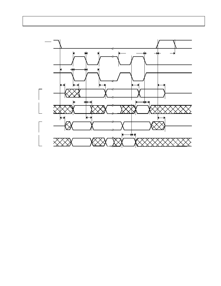
35(/,0,1$5< 7(&+1,&$/ '$7$
This information applies to a product under development. Its characteristics and specifications are subject to change with-
out notice. Analog Devices assumes no obligation regarding future manufacturing unless otherwise agreed to in writing.
49
REV. PrA
For current information contact Analog Devices at 800/262-5643
ADSP-2195
September 2001
Figure 24. Serial Peripheral Interface (SPI) Port--Slave
W
+ 6 3 , '
W
' ' 6 3 , '
W
' 6 ' + ,
/ 6 %
0 6 %
0 6 %
9 $ / ,'
W
+ 6 3 , '
W
' 6 2 (
W
' ' 6 3 , '
W
+ ' 6 3 , '
0 ,6 2
2 8 7 3 8 7
0 2 6 ,
, 1 3 8 7
W
6 6 3 , '
6 3 , 6 6
, 1 3 8 7
6 & / .
& 3 2 /
, 1 3 8 7
6 & / .
& 3 2 /
, 1 3 8 7
W
6 ' 6 & ,
W
6 3 , & + 6
W
6 3 , & / 6
W
6 3 , & / 6
W
6 3 , & / .
W
+ ' 6
W
6 3 , & + 6
W
6 6 3 , '
W
+ 6 3 , '
W
' 6 ' + ,
/ 6 %
9 $ / , '
0 6 %
0 6 %
9 $ / ,'
W
' 6 2 (
W
' ' 6 3 , '
0 ,6 2
2 8 7 3 8 7
0 2 6 ,
, 1 3 8 7
W
6 6 3 , '
/ 6 %
9 $ / ,'
/ 6 %
& 3 + $
& 3 + $
W
6 3 , 7 ' 6
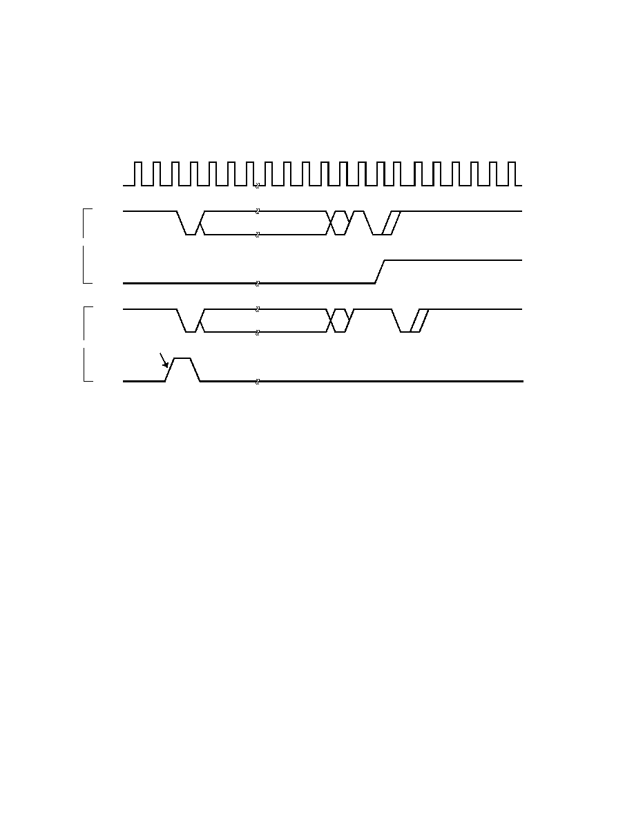
For current information contact Analog Devices at 800/262-5643
ADSP-2195
September 2001
This information applies to a product under development. Its characteristics and specifications are subject to change with-
out notice. Analog Devices assumes no obligation regarding future manufacturing unless otherwise agreed to in writing.
50
REV. PrA
35(/,0,1$5< 7(&+1,&$/ '$7$
Universal Asynchronous Receiver-Transmitter (UART)
Port--Receive and Transmit Timing
Figure 25
describes UART port receive and transmit oper-
ations. The maximum baud rate is HCLK/16. As shown in
Figure 25
there is some latency between the generation
internal UART interrupts and the external data operations.
These latencies are negligible at the data transmission rates
for the UART.
Figure 25. UART Port--Receive and Transmit Timing
5 ; '
' $ 7 $ ±
,1 7 ( 5 1 $ /
8 $ 5 7 5 ( & ( , 9 (
,1 7 ( 5 5 8 3 7
8 $ 5 7 5 ( & ( , 9 ( % , 7 6 ( 7 % < ' $ 7 $ 6 7 2 3
& / ( $ 5 ( ' % < ) , ) 2 5 ( $ '
+ & / .
6 $ 0 3 / (
& / 2 & .
7 ; '
' $ 7 $ ±
6 7 2 3 ±
, 1 7 ( 5 1 $ /
8 $ 5 7 7 5 $ 1 6 0 , 7
,1 7 ( 5 5 8 3 7
8 $ 5 7 7 5 $ 1 6 0 , 7 % ,7 6 ( 7 % < 3 5 2 * 5 $ 0
& / ( $ 5 ( ' % < : 5 , 7 ( 7 2 7 5 $ 1 6 0 ,7
6 7 $ 5 7
6 7 2 3
7 5 $ 1 6 0 , 7
5 ( & ( , 9 (
$ 6 ' $ 7 $
: 5 ,7 ( 1 7 2
% 8 ) ) ( 5
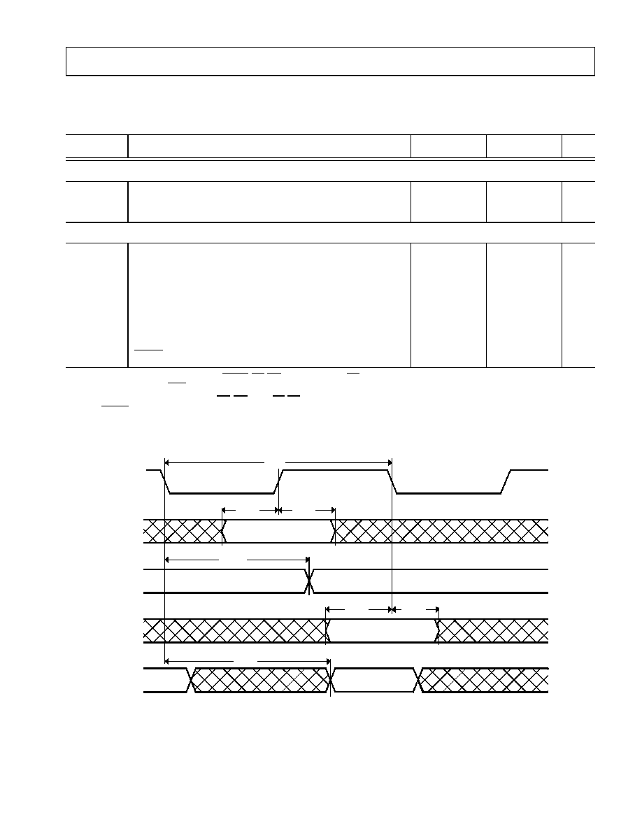
This information applies to a product under development. Its characteristics and specifications are subject to change with-
out notice. Analog Devices assumes no obligation regarding future manufacturing unless otherwise agreed to in writing.
51
REV. PrA
For current information contact Analog Devices at 800/262-5643
ADSP-2195
September 2001
35(/,0,1$5< 7(&+1,&$/ '$7$
JTAG Test And Emulation Port Timing
Table 22
and
Figure 26
describe JTAG port operations.
Table 22. JTAG Port Timing
Parameter
Description
Min
Max
Unit
Switching Characteristics
t
DTDO
TDO Delay from TCK Low
4
ns
t
DSYS
System Outputs Delay After TCK Low
1
0
5
ns
Timing Parameters
t
TCK
TCK Period
20
ns
t
STAP
TDI, TMS Setup Before TCK High
4
ns
t
HTAP
TDI, TMS Hold After TCK High
4
ns
t
SSYS
System Inputs Setup Before TCK Low
2
4
ns
t
HSYS
System Inputs Hold After TCK Low
2
5
ns
t
TRSTW
TRST Pulsewidth
3
4
ns
1
System Outputs = DATA150, ADDR210, MS30, RD, WR, ACK, CLKOUT, BG, PF70, TIMEXP, DT0, DT1, TCLK0, TCLK1, RCLK0, RCLK1,
TFS0, TFS1, RFS0, RFS1, BMS.
2
System Inputs = DATA150, ADDR210, RD, WR, ACK, BR, BG, PF70, DR0, DR1, TCLK0, TCLK1, RCLK0, RCLK1, TFS0, TFS1, RFS0, RFS1,
CLKIN, RESET.
3
50 MHz max.
Figure 26. JTAG Port Timing
7 0 6
7 ' ,
7 ' 2
6 < 6 7 ( 0
,1 3 8 7 6
6 < 6 7 ( 0
2 8 7 3 8 7 6
7 & .
W
7 & .
W
+ 7 $ 3
W
6 7 $ 3
W
' 7 ' 2
W
6 6 < 6
W
+ 6 < 6
W
' 6 < 6
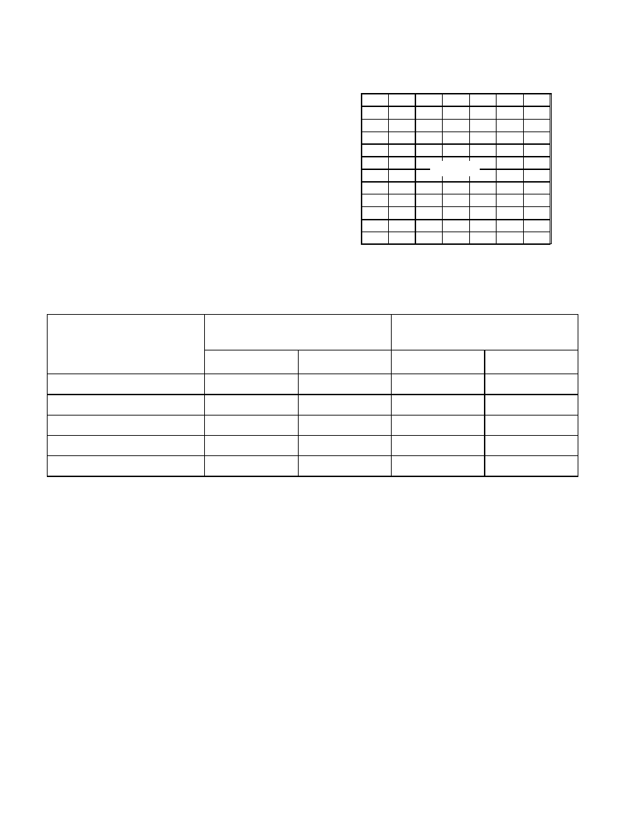
For current information contact Analog Devices at 800/262-5643
ADSP-2195
September 2001
This information applies to a product under development. Its characteristics and specifications are subject to change with-
out notice. Analog Devices assumes no obligation regarding future manufacturing unless otherwise agreed to in writing.
52
REV. PrA
35(/,0,1$5< 7(&+1,&$/ '$7$
Output Drive Currents
Figure 27
shows typical I-V characteristics for the output
drivers of the ADSP-2195. The curves represent the current
drive capability of the output drivers as a function of output
voltage.
Power Dissipation
Total power dissipation has two components, one due to
internal circuitry and one due to the switching of external
output drivers. Internal power dissipation is dependent on
the instruction execution sequence and the data operands
involved. Using the current current-versus-operation infor-
mation in
Table 23
, designers can estimate the
ADSP-2195's internal power supply (V
DDINT
) input current
for a specific application, according to the formula in
Figure 28
.
The external component of total power dissipation is caused
by the switching of output pins. Its magnitude depends on:
· The number of output pins that switch during each cycle
(O)
· The maximum frequency at which they can switch (f)
· Their load capacitance (C)
· Their voltage swing (V
DD
)
and is calculated by the formula in
Figure 29
.
Figure 27. ADSP-2195 Typical Drive Currents
6285&( 9
''( ;7
92/7$*( ± 9
±
62
8
5
&
(
9
''(
;7
&
85
5
(
1
7
±
P
$
7%'
±
±
±
±
±
Table 23. ADSP-2195 Operation Types Versus Input Current
Activity
I
DD
(mA)
1
CCLK = 80 MHz
I
DD
(mA)
1
CCLK = 160 MHz
Core
Peripheral
Core
Peripheral
Power down
2
0
0
0
0
Idle 1
3
0
3
0
5
Idle 2
4
0
30
0
60
Typical
5
95
30
184
60
Peak
6
112
30
215
60
1
Test conditions: V
DD
= 2.50 V; HCLK (peripheral clock) frequency = CCLK/2 (core clock/2) frequency; T
AMB
= 25 ºC.
2
PLL, Core, peripheral clocks, and CLKIN are disabled.
3
PLL is enabled and Core and peripheral clocks are disabled.
4
Core CLK is disabled and peripheral clock is enabled. This is a power- down interrupt mode. The timer can be used to generate an interrupt to enable the
Core clock.
5
All instructions execute from internal memory. 100% of the instructions are MAC with dual operand addressing, with changing data fetched using a linear
address sequence, and 50% of the instructions move data from PM to a data register.
6
All instructions execute from internal memory. 50% of the instructions are repeat MACs with dual operand addressing, with changing data fetched using
a linear address sequence.
Figure 28. I
DDINT
Calculation
I
DDINT
%Typical
I
DD-TYPICAL
×
(
)
=
%Idle
I
DD-IDLE
×
(
)
%Powerdown
I
DD-PWRDWN
×
(
)
+
+

This information applies to a product under development. Its characteristics and specifications are subject to change with-
out notice. Analog Devices assumes no obligation regarding future manufacturing unless otherwise agreed to in writing.
53
REV. PrA
For current information contact Analog Devices at 800/262-5643
ADSP-2195
September 2001
35(/,0,1$5< 7(&+1,&$/ '$7$
The load capacitance should include the processor's
package capacitance (C
IN
). The switching frequency
includes driving the load high and then back low. Address
and data pins can drive high and low at a maximum rate of
1/(2t
CK
). The write strobe can switch every cycle at a
frequency of 1/t
CK
. Select pins switch at 1/(2t
CK
), but selects
can switch on each cycle. For example, estimate P
EXT
with
the following assumptions:
· A system with one bank of external data memory--asyn-
chronous RAM (16-bit)
· One 64K 16 RAM chip is used with a load of 10 pF
· Maximum peripheral speed HCLK = 100 MHz
· External data memory writes occur every other cycle, a
rate of 1/(4t
HCLK
), with 50% of the pins switching
· The bus cycle time is 100 MHz (t
HCLK
= 10 nsec)
Figure 29. P
EXT
Calculation
P
EXT
O
C
×
V
DD
2
×
f
×
=
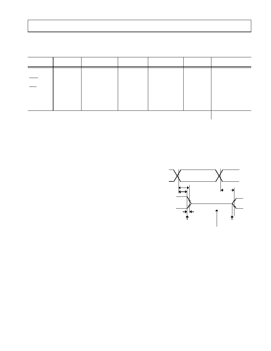
This information applies to a product under development. Its characteristics and specifications are subject to change with-
out notice. Analog Devices assumes no obligation regarding future manufacturing unless otherwise agreed to in writing.
54
REV. PrA
For current information contact Analog Devices at 800/262-5643
ADSP-2195
September 2001
35(/,0,1$5< 7(&+1,&$/ '$7$
The P
EXT
equation is calculated for each class of pins that
can drive as shown in
Table 24
.
A typical power consumption can now be calculated for
these conditions by adding a typical internal power dissipa-
tion with the formula in
Figure 30
.
Where:
· P
EXT
is from
Table 24
· P
INT
is I
DDINT
2.5V, using the calculation I
DDINT
listed in
Power Dissipation on page 52
Note that the conditions causing a worst-case P
EXT
are
different from those causing a worst-case P
INT
. Maximum
P
INT
cannot occur while 100% of the output pins are
switching from all ones to all zeros. Note also that it is not
common for an application to have 100% or even 50% of
the outputs switching simultaneously.
Test Conditions
The DSP is tested for output enable, disable, and hold time.
Output Disable Time
Output pins are considered to be disabled when they stop
driving, go into a high impedance state, and start to decay
from their output high or low voltage. The time for the
voltage on the bus to decay by V is dependent on the
capacitive load, C
L
and the load current, I
L
. This decay time
can be approximated by the equation in
Figure 31
.
The output disable time t
DIS
is the difference between
t
MEASURED
and t
DECAY
as shown in
Figure 32
. The time
t
MEASURED
is the interval from when the reference signal
switches to when the output voltage decays V from the
measured output high or output low voltage. The t
DECAY
is
calculated with test loads C
L
and I
L
, and with V equal to
0.5 V.
Output Enable Time
Output pins are considered to be enabled when they have
made a transition from a high impedance state to when they
start driving. The output enable time t
ENA
is the interval
from when a reference signal reaches a high or low voltage
level to when the output has reached a specified high or low
trip point, as shown in the Output Enable/Disable diagram
(
Figure 32
). If multiple pins (such as the data bus) are
enabled, the measurement value is that of the first pin to
start driving.
Table 24. P
EXT
Calculation
Pin Type
# of Pins
% Switching
C
f
V
DD
2
= P
EXT
Address
15
50
TBD pF
25.0 MHz
10.9 V
= TBD W
MSx
1
0
TBD pF
25.0 MHz
10.9 V
= TBD W
WR
1
--
TBD pF
25 MHz
10.9 V
= TBD W
Data
16
50
TBD pF
25.0 MHz
10.9 V
= TBD W
CLKOUT
1
--
TBD pF
100 MHz
10.9 V
= TBD W
P
EXT
=TBD W
Figure 30. P
TOTAL
(Typical) Calculation
Figure 31. Decay Time Calculation
P
TOTAL
P
=
EXT
P
INT
+
t
DECAY
C
L
V
I
L
---------------
=
Figure 32. Output Enable/Disable
5()(5(1&(
6,*1$/
W
',6
287387 67$576
'5,9,1*
9
2+ 0( $685('
± '9
9
2/ 0( $685('
'9
W
0 ($ 685( '
9
2+ 0( $6 85 ('
9
2/ 0( $6 85 ('
9
9
+,*+,0 3('$1&( 67$7(
7(67 &21',7,216 &$86( 7+,692/7$*(
72 %( $3352;,0 $7(/< 9
287387 67236
'5,9,1*
W
' (&$<
W
( 1$
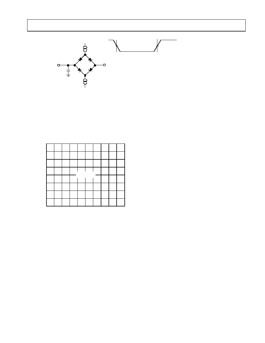
This information applies to a product under development. Its characteristics and specifications are subject to change with-
out notice. Analog Devices assumes no obligation regarding future manufacturing unless otherwise agreed to in writing.
55
REV. PrA
For current information contact Analog Devices at 800/262-5643
ADSP-2195
September 2001
35(/,0,1$5< 7(&+1,&$/ '$7$
Example System Hold
Time Calculation
To determine the data output
hold time in a particular
system, first calculate t
DECAY
using the equation given in
Figure 31
. Choose V to be
the difference between the
ADSP-2195's output voltage
and the input threshold for
the device requiring the hold
time. A typical V will be
0.4 V. C
L
is the total bus
capacitance (per data line),
and I
L
is the total leakage or
three-state current (per data
line). The hold time will be
t
DECAY
plus the minimum
disable time (i.e., t
DATRWH
for
the write cycle).
Capacitive Loading
Output delays and holds are
based on standard capacitive
loads: 50 pF on all pins (see
Figure 37
). The delay and
hold specifications given
should be derated by a factor
of 1.5 ns/50 pF for loads
other than the nominal value
of 50 pF.
Figure 35
and
Figure 36
show how output
rise time varies with capaci-
tance. These figures also
show graphically how output
delays and holds vary with
load capacitance. (Note that
this graph or derating does
not apply to output disable
delays; see
Output Disable
Time on page 54
.) The
graphs in these figures may
not be linear outside the
ranges shown.
Environmental Conditions
The thermal characteristics
in which the DSP is operating
influence performance.
Thermal Characteristics
The ADSP-2195 comes in a
144-lead LQFP or 144-lead
Ball Grid Array (mini-BGA)
package. The ADSP-2195 is
specified for an ambient tem-
perature (T
AMB
) as calculated
using the formula in
Figure 38
. To ensure that the
T
AMB
data sheet specification
is not exceeded, a heatsink
and/or an air flow source may
be used. A heatsink should be
attached to the ground plane
(as close as possible to the
thermal pathways) with a
thermal adhesive.
Where:
· T
AMB
= Ambient tempera-
ture (measured near top
surface of package)
· PD = Power dissipation in
W (this value depends
upon the specific applica-
tion; a method for
calculating PD is shown
under Power Dissipation).
·
CA
= Value from
Table 25
.
·
JB
= TBD°C/W
There are some important
things to note about these
T
AMB
calculations and the
values in
Table 25
:
· This represents thermal
resistance at total power of
TBD W.
· For the LQFP package:
JC
= 0.96°C/W
For the mini-BGA
package:
JC
= 8.4°C/W
Figure 33. Equivalent
Device Loading
for AC
Measurements
(Includes All
Fixtures)
9
S)
72
287387
3,1
,
2/
,
2+
Figure
34.
Voltage
Reference
Levels
for
AC
Measurements
(Except
Output
Enable/Disable)
,1387
25
287387
9
9
Figure 35. Typical Output Rise Time (10%90%,
V
DDEXT
=Max) vs. Load Capacitance
/2$' &$3 $&,7$1&( ±S)
7%'
5,
6
(
$
1'
)
$/
/
7
,
0
(
6
±
QV
9
±
9
±
For current information contact Analog Devices at 800/262-5643
ADSP-2195
September 2001
This information applies to a product under development. Its characteristics and specifications are subject to change with-
out notice. Analog Devices assumes no obligation regarding future manufacturing unless otherwise agreed to in writing.
56
REV. PrA
35(/,0,1$5< 7(&+1,&$/ '$7$
Figure 36. Typical Output Rise Time (10%-90%,
V
DDEXT
=Min) vs. Load Capacitance
Figure 37. Typical Output Delay or Hold vs. Load Capacitance (at Max Case Temperature)
Figure 38. T
CASE
Calculation
Table 25.
CA
Values
1
Airflow
(Linear Ft./Min.)
0
100
200
400
600
Airflow
(Meters/Second)
0
0.5
1
2
3
LQFP:
CA
(°C/W)
44.3
41.4
38.5
35.3
32.1
Mini-BGA:
CA
(°C/W)
26
24
22
20.9
19.8
/2$' &$3 $&,7$1&( ±S)
7%'
5,
6
(
$1'
)
$/
/
7
,
0
(
6
±
QV
±
±
/2$' &$3 $&,7$1&( ±S)
±
120 ,1$/
7%'
2
8
7
3
8
7
'
(
/
$
<
2
5
+
2
/
'
±
QV
T
AMB
T
CASE
=
PD
CA
×

For current information contact Analog Devices at 800/262-5643
ADSP-2195
September 2001
This information applies to a product under development. Its characteristics and specifications are subject to change with-
out notice. Analog Devices assumes no obligation regarding future manufacturing unless otherwise agreed to in writing.
57
REV. PrA
35(/,0,1$5< 7(&+1,&$/ '$7$
1
These are preliminary estimates.

For current information contact Analog Devices at 800/262-5643
ADSP-2195
September 2001
This information applies to a product under development. Its characteristics and specifications are subject to change with-
out notice. Analog Devices assumes no obligation regarding future manufacturing unless otherwise agreed to in writing.
58
REV. PrA
35(/,0,1$5< 7(&+1,&$/ '$7$
ADSP-2195 144-Lead
LQFP Pinout
Table 26
lists the LQFP
pinout by signal name.
Table 26. 144-Lead LQFP
Pins (Alphabetically By
Signal)
SIGNAL
PIN #
A0
84
A1
85
A2
86
A3
87
A4
88
A5
89
A6
91
A7
92
A8
93
A9
95
A10
96
A11
97
A12
98
A13
99
A14
101
A15
102
A16
103
A17
104
A18
106
A19
107
A20
108
A21
109
ACK
120
BG
111
BGH
110
BMODE0
70
BMODE1
71
BMS
113
BR
112
BYPASS
72
CLKOUT
130
D0
123
D1
124
D2
125
D3
126
D4
128
D5
135
D6
136
D7
137
D8
138
D9
139
D10
140
D11
141
D12
142
D13
144
D14
1
D15
2
DR0
60
DR1
67
DR2
49
DT0
56
DT1
64
DT2
46
EMU
81
HACK
26
HACK_P
24
Table 26. 144-Lead LQFP
Pins (Alphabetically By
Signal) (Continued)
SIGNAL
PIN #
HAD0
3
HAD1
4
HAD2
6
HAD3
7
HAD4
8
HAD5
9
HAD6
10
HAD7
11
HAD8
12
HAD9
14
HAD10
15
HAD11
17
HAD12
18
HAD13
20
HAD14
21
HAD15
22
HA16
23
HALE
30
HCMS
27
HCIOMS
28
HRD
31
HWR
32
IOMS
114
MS0
115
MS1
116
MS2
117
MS3
119
OPMODE
83
CLKIN
132
XTAL
133
Table 26. 144-Lead LQFP
Pins (Alphabetically By
Signal) (Continued)
SIGNAL
PIN #
PF0
34
PF1
35
PF2
36
PF3
37
PF4
38
PF5
39
PF6
41
PF7
42
RCLK0
61
RCLK1
68
RCLK2
50
RESET
73
RFS0
62
RFS1
69
RFS2
51
RD
122
RXD
52
TCK
78
TCLK0
57
TCLK1
65
TCLK2
47
TDI
75
TDO
74
TFS0
59
TFS1
66
TFS2
48
TMR0
43
TMR1
44
TMR2
45
TMS
76
Table 26. 144-Lead LQFP
Pins (Alphabetically By
Signal) (Continued)
SIGNAL
PIN #

For current information contact Analog Devices at 800/262-5643
ADSP-2195
September 2001
This information applies to a product under development. Its characteristics and specifications are subject to change with-
out notice. Analog Devices assumes no obligation regarding future manufacturing unless otherwise agreed to in writing.
59
REV. PrA
35(/,0,1$5< 7(&+1,&$/ '$7$
Table 27
lists the LQFP
pinout by pin number.
TRST
79
TXD
53
V
DDEXT
13
V
DDEXT
25
V
DDEXT
40
V
DDEXT
63
V
DDEXT
90
V
DDEXT
100
V
DDEXT
118
V
DDEXT
131
V
DDEXT
143
V
DDINT
19
V
DDINT
58
V
DDINT
82
V
DDINT
127
GND
5
GND
16
GND
29
GND
33
GND
54
GND
55
GND
77
GND
80
GND
94
GND
105
GND
129
GND
134
WR
121
Table 26. 144-Lead LQFP
Pins (Alphabetically By
Signal) (Continued)
SIGNAL
PIN #
Table 27. 144-Lead LQFP
Pins (Numerically By Pin
Number
SIGNAL
PIN #
D14
1
D15
2
HAD0
3
HAD1
4
GND
5
HAD2
6
HAD3
7
HAD4
8
HAD5
9
HAD6
10
HAD7
11
HAD8
12
V
DDEXT
13
HAD9
14
HAD10
15
GND
16
HAD11
17
HAD12
18
V
DDINT
19
HAD13
20
HAD14
21
HAD15
22
HA16
23
HACK_P
24
V
DDEXT
25
HACK
26
HCMS
27
HCIOMS
28
GND
29
HALE
30
HRD
31
HWR
32
GND
33
PF0
34
PF1
35
PF2
36
PF3
37
PF4
38
PF5
39
V
DDEXT
40
PF6
41
PF7
42
TMR0
43
TMR1
44
TMR2
45
DT2
46
TCLK2
47
TFS2
48
DR2
49
RCLK2
50
RFS2
51
RXD
52
TXD
53
GND
54
GND
55
DT0
56
TCLK0
57
V
DDINT
58
Table 27. 144-Lead LQFP
Pins (Numerically By Pin
Number (Continued)
SIGNAL
PIN #
TFS0
59
DR0
60
RCLK0
61
RFS0
62
V
DDEXT
63
DT1
64
TCLK1
65
TFS1
66
DR1
67
RCLK1
68
RFS1
69
BMODE0
70
BMODE1
71
BYPASS
72
RESET
73
TDO
74
TDI
75
TMS
76
GND
77
TCK
78
TRST
79
GND
80
EMU
81
V
DDINT
82
OPMODE
83
A0
84
A1
85
A2
86
A3
87
A4
88
Table 27. 144-Lead LQFP
Pins (Numerically By Pin
Number (Continued)
SIGNAL
PIN #

For current information contact Analog Devices at 800/262-5643
ADSP-2195
September 2001
This information applies to a product under development. Its characteristics and specifications are subject to change with-
out notice. Analog Devices assumes no obligation regarding future manufacturing unless otherwise agreed to in writing.
60
REV. PrA
35(/,0,1$5< 7(&+1,&$/ '$7$
A5
89
V
DDEXT
90
A6
91
A7
92
A8
93
GND
94
A9
95
A10
96
A11
97
A12
98
A13
99
V
DDEXT
100
A14
101
A15
102
A16
103
A17
104
GND
105
A18
106
A19
107
A20
108
A21
109
BGH
110
BG
111
BR
112
BMS
113
IOMS
114
MS0
115
MS1
116
MS2
117
V
DDEXT
118
Table 27. 144-Lead LQFP
Pins (Numerically By Pin
Number (Continued)
SIGNAL
PIN #

This information applies to a product under development. Its characteristics and specifications are subject to change with-
out notice. Analog Devices assumes no obligation regarding future manufacturing unless otherwise agreed to in writing.
61
REV. PrA
For current information contact Analog Devices at 800/262-5643
ADSP-2195
September 2001
35(/,0,1$5< 7(&+1,&$/ '$7$
MS3
119
ACK
120
WR
121
RD
122
D0
123
D1
124
D2
125
D3
126
V
DDINT
127
D4
128
GND
129
CLKOUT
130
V
DDEXT
131
CLKIN
132
XTAL
133
GND
134
D5
135
D6
136
D7
137
D8
138
D9
139
D10
140
D11
141
D12
142
V
DDEXT
143
D13
144
Table 27. 144-Lead LQFP
Pins (Numerically By Pin
Number (Continued)
SIGNAL
PIN #

This information applies to a product under development. Its characteristics and specifications are subject to change with-
out notice. Analog Devices assumes no obligation regarding future manufacturing unless otherwise agreed to in writing.
62
REV. PrA
For current information contact Analog Devices at 800/262-5643
ADSP-2195
September 2001
35(/,0,1$5< 7(&+1,&$/ '$7$
ADSP-2195 144-Lead Mini-BGA Pinout
Table 28
lists the mini-BGA pinout by signal name.
Table 28. 144-Lead Mini-BGA Pins (Alphabetically By
Signal)
SIGNAL
BALL #
A0
J11
A1
H9
A2
H10
A3
G12
A4
H11
A5
G10
A6
F12
A7
G11
A8
F10
A9
F11
A10
E12
A11
E11
A12
E10
A13
E9
A14
D11
A15
D10
A16
D12
A17
C11
A18
C12
A19
B12
A20
B11
A21
A11
ACK
A8
BG
C10
BGH
B10
BMODE0
L10
BMODE1
L9
BMS
A10
BR
B9
BYPASS
M11
CLKIN
A5
CLKOUT
C6
D0
D7
D1
A7
D2
C7
D3
A6
D4
B7
D5
A4
D6
C5
D7
B5
D8
D5
D9
A3
D10
C4
D11
B4
D12
C3
D13
A2
D14
B1
D15
B2
DR0
L7
DR1
K9
DR2
L5
TCLK0
J6
DT1
L8
DT2
H4
EMU
J10
HACK
H3
HACK_P
G1
Table 28. 144-Lead Mini-BGA Pins (Alphabetically By
Signal)
(Continued)
SIGNAL
BALL #

This information applies to a product under development. Its characteristics and specifications are subject to change with-
out notice. Analog Devices assumes no obligation regarding future manufacturing unless otherwise agreed to in writing.
63
REV. PrA
For current information contact Analog Devices at 800/262-5643
ADSP-2195
September 2001
35(/,0,1$5< 7(&+1,&$/ '$7$
HAD0
C1
HAD1
B3
HAD2
C2
HAD3
D1
HAD4
D4
HAD5
D3
HAD6
D2
HAD7
E1
HAD8
E4
HAD9
E2
HAD10
F1
HAD11
E3
HAD12
F2
HAD14
F3
HAD15
G3
HAD13
G2
HA16
H2
HALE
J1
HCIOMS
J3
HCMS
H1
HRD
J2
HWR
K2
IOMS
E8
MS0
D9
MS1
A9
MS2
C9
MS3
D8
OPMODE
H12
PF0
K1
PF1
L1
Table 28. 144-Lead Mini-BGA Pins (Alphabetically By
Signal)
(Continued)
SIGNAL
BALL #
PF2
M2
PF3
L2
PF4
M3
PF5
L3
PF6
K3
PF7
M4
RCLK0
K7
RCLK1
J9
RCLK2
J5
RD
B8
RESET
L12
RFS0
K8
RFS1
M10
RFS2
M6
RXD
K6
TCK
K11
DT0
H6
TCLK1
M9
TCLK2
K5
TDI
K12
TDO
L11
TFS0
M8
TFS1
J8
TFS2
M5
TMR0
K4
TMR1
L4
TMR2
J4
TMS
K10
TRST
J12
TXD
M7
Table 28. 144-Lead Mini-BGA Pins (Alphabetically By
Signal)
(Continued)
SIGNAL
BALL #

This information applies to a product under development. Its characteristics and specifications are subject to change with-
out notice. Analog Devices assumes no obligation regarding future manufacturing unless otherwise agreed to in writing.
64
REV. PrA
For current information contact Analog Devices at 800/262-5643
ADSP-2195
September 2001
35(/,0,1$5< 7(&+1,&$/ '$7$
Table 29
lists the mini-BGA pinout by ball number.
V
DDINT
D6
V
DDINT
F4
V
DDINT
G9
V
DDINT
J7
V
DDEXT
E5
V
DDEXT
E6
V
DDEXT
F5
V
DDEXT
F6
V
DDEXT
G7
V
DDEXT
G8
V
DDEXT
H7
V
DDEXT
H8
GND
A1
GND
A12
GND
E7
GND
F7
GND
F8
GND
F9
GND
G4
GND
G5
GND
G6
GND
H5
GND
L6
GND
M1
GND
M12
WR
C8
XTAL
B6
Table 28. 144-Lead Mini-BGA Pins (Alphabetically By
Signal)
(Continued)
SIGNAL
BALL #
Table 29. 144-Lead Mini-BGA Pins (Numerically By
Ball Number)
SIGNAL
BALL #
GND
A1
D13
A2
D9
A3
D5
A4
CLKIN
A5
D3
A6
D1
A7
ACK
A8
MS1
A9
BMS
A10
A21
A11
GND
A12
D14
B1
D15
B2
HAD1
B3
D11
B4
D7
B5
XTAL
B6
D4
B7
RD
B8
BR
B9
BGH
B10
A20
B11
A19
B12
HAD0
C1
HAD2
C2
D12
C3
D10
C4
D6
C5

This information applies to a product under development. Its characteristics and specifications are subject to change with-
out notice. Analog Devices assumes no obligation regarding future manufacturing unless otherwise agreed to in writing.
65
REV. PrA
For current information contact Analog Devices at 800/262-5643
ADSP-2195
September 2001
35(/,0,1$5< 7(&+1,&$/ '$7$
CLKOUT
C6
D2
C7
WR
C8
MS2
C9
BG
C10
A17
C11
A18
C12
HAD3
D1
HAD6
D2
HAD5
D3
HAD4
D4
D8
D5
V
DDINT
D6
D0
D7
MS3
D8
MS0
D9
A15
D10
A14
D11
A16
D12
HAD7
E1
HAD9
E2
HAD11
E3
HAD8
E4
V
DDEXT
E5
V
DDEXT
E6
GND
E7
IOMS
E8
A13
E9
A12
E10
A11
E11
Table 29. 144-Lead Mini-BGA Pins (Numerically By
Ball Number) (Continued)
SIGNAL
BALL #
A10
E12
HAD10
F1
HAD12
F2
HAD14
F3
V
DDINT
F4
V
DDEXT
F5
V
DDEXT
F6
GND
F7
GND
F8
GND
F9
A8
F10
A9
F11
A6
F12
HACK_P
G1
HAD13
G2
HAD15
G3
GND
G4
GND
G5
GND
G6
V
DDEXT
G7
V
DDEXT
G8
V
DDINT
G9
A5
G10
A7
G11
A3
G12
HCMS
H1
HA16
H2
HACK
H3
DT2
H4
GND
H5
Table 29. 144-Lead Mini-BGA Pins (Numerically By
Ball Number) (Continued)
SIGNAL
BALL #

This information applies to a product under development. Its characteristics and specifications are subject to change with-
out notice. Analog Devices assumes no obligation regarding future manufacturing unless otherwise agreed to in writing.
66
REV. PrA
For current information contact Analog Devices at 800/262-5643
ADSP-2195
September 2001
35(/,0,1$5< 7(&+1,&$/ '$7$
DT0
H6
V
DDEXT
H7
V
DDEXT
H8
A1
H9
A2
H10
A4
H11
OPMODE
H12
HALE
J1
HRD
J2
HCIOMS
J3
TMR2
J4
RCLK2
J5
TCLK0
J6
V
DDINT
J7
TFS1
J8
RCLK1
J9
EMU
J10
A0
J11
TRST
J12
PF0
K1
HWR
K2
PF6
K3
TMR0
K4
TCLK2
K5
RXD
K6
RCLK0
K7
RFS0
K8
DR1
K9
TMS
K10
TCK
K11
Table 29. 144-Lead Mini-BGA Pins (Numerically By
Ball Number) (Continued)
SIGNAL
BALL #
TDI
K12
PF1
L1
PF3
L2
PF5
L3
TMR1
L4
DR2
L5
GND
L6
DR0
L7
DT1
L8
BMODE1
L9
BMODE0
L10
TDO
L11
RESET
L12
GND
M1
PF2
M2
PF4
M3
PF7
M4
TFS2
M5
RFS2
M6
TXD
M7
TFS0
M8
TCLK1
M9
RFS1
M10
BYPASS
M11
GND
M12
Table 29. 144-Lead Mini-BGA Pins (Numerically By
Ball Number) (Continued)
SIGNAL
BALL #
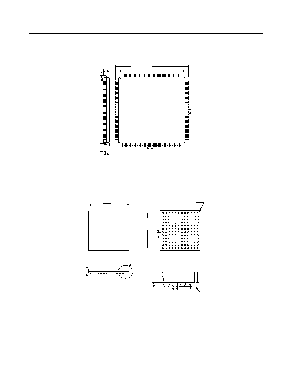
This information applies to a product under development. Its characteristics and specifications are subject to change with-
out notice. Analog Devices assumes no obligation regarding future manufacturing unless otherwise agreed to in writing.
67
REV. PrA
For current information contact Analog Devices at 800/262-5643
ADSP-2195
September 2001
35(/,0,1$5< 7(&+1,&$/ '$7$
OUTLINE DIMENSIONS
.
144-LEAD METRIC THIN PLASTIC QUAD FLATPACK (LQFP) (ST-144)
144-BALL MINI-BGA (CA-144)
6($7,1*
3/$1(
0 $;
0 $;
723 9,(:
3,16 ' 2: 1
%6& 64
%6& 64
%6&
/($' 3,7&+
',0(16,216 ,1 0,//,0 (7(56
$&78$/ 326,7,21 2) ($&+ /($' ,6 : ,7+,1 2) ,76
,'($/ 326,7,21 : +(1 0 ($685(' ,1 7+( /$7(5$/ ',5(&7,21
&(17(5 ',0 (16,216 $5( 120 ,1$/
127(6
7<3
6($7,1*
3/$1(
',0(16,216 ,1 0 ,//,0 (7(56
$&78$/ 326,7,21 2) 7+( %$// *5,' ,6
: ,7+,1 2) ,76 ,'($/ 326,7,21 5(/$7,9( 72
7+( 3$&.$*( ('*(6
$&78$/ 326,7,21 2) ($&+ %$// ,6 : ,7+,1
2) ,76 ,'($/ 326,7,21 5(/$7,9( 72 7+( %$//
*5,'
&(17(5 ',0(16,216 $5( 120 ,1$/
127(6
'(7$,/ $
%$//
',$0 (7(5
0 $;
0 $;
'(7$,/ $
%6&
%$//
3,7&+
%6&
64
$
%
&
'
(
)
*
+
-
.
/
0
64
%27720 9,(:
723 9,(:
$ & 2 5 1 ( 5 , 1 ' ( ;
7 5 , $ 1 * / (

This information applies to a product under development. Its characteristics and specifications are subject to change with-
out notice. Analog Devices assumes no obligation regarding future manufacturing unless otherwise agreed to in writing.
68
REV. PrA
For current information contact Analog Devices at 800/262-5643
ADSP-2195
September 2001
35(/,0,1$5< 7(&+1,&$/ '$7$
ORDERING GUIDE
Part Number
1,
2
1
ST = Plastic Thin Quad Flatpack (LQFP).
2
CA = Mini Ball Grid Array
Ambient Temperature Range
Instruction Rate On-Chip SRAM
Operating Voltage
ADSP-2195MKST-160X
0ºC to 70ºC
160 MHz
1.3M bit
2.5 Int./3.3 Ext. V
ADSP-2195MBST-140X
-40ºC to 85ºC
140 MHz
1.3M bit
2.5 Int./3.3 Ext. V
ADSP-2195MKCA-160X 0ºC to 70ºC
160 MHz
1.3M bit
2.5 Int./3.3 Ext. V
ADSP-2195MBCA-140X -40ºC to 85ºC
140 MHz
1.3M bit
2.5 Int./3.3 Ext. V
Document Outline