Äîêóìåíòàöèÿ è îïèñàíèÿ www.docs.chipfind.ru
a
Mixed Signal DSP Controller
Information furnished by Analog Devices is believed to be accurate and
reliable. However, no responsibility is assumed by Analog Devices for its
use, nor for any infringements of patents or other rights of third parties that
may result from its use. No license is granted by implication or otherwise
under any patent or patent rights of Analog Devices. Trademarks and
registered trademarks are the property of their respective companies.
REV. 0
ADSP-21990
KEY FEATURES
ADSP-219x, 16-Bit, Fixed Point DSP Core with up to
160 MIPS Sustained Performance
8K Words of On-Chip RAM, Configured as 4K Words On-
Chip 24-Bit Program RAM and 4K Words On-Chip
16-Bit Data RAM
External Memory Interface
Dedicated Memory DMA Controller for Data/Instruction
Transfer between Internal/External Memory
Programmable PLL and Flexible Clock Generation
Circuitry Enables Full Speed Operation from Low
Speed Input Clocks
IEEE JTAG Standard 1149.1 Test Access Port Supports
On-Chip Emulation and System Debugging
8-Channel, 14-Bit Analog-to-Digital Converter System,
with up to 20 MSPS Sampling Rate (at 160 MHz Core
Clock Rate)
Three Phase 16-Bit Center Based PWM Generation Unit
with 12.5 ns Resolution at 160 MHz Core Clock (CCLK)
Rate
Dedicated 32-Bit Encoder Interface Unit with
Companion Encoder Event Timer
Dual 16-Bit Auxiliary PWM Outputs
16 General-Purpose Flag I/O Pins
Three Programmable 32-Bit Interval Timers
SPI Communications Port with Master or Slave
Operation
Synchronous Serial Communications Port (SPORT)
Capable of Software UART Emulation
Integrated Watchdog Timer
Dedicated Peripheral Interrupt Controller with Software
Priority Control
Multiple Boot Modes
Precision 1.0 V Voltage Reference
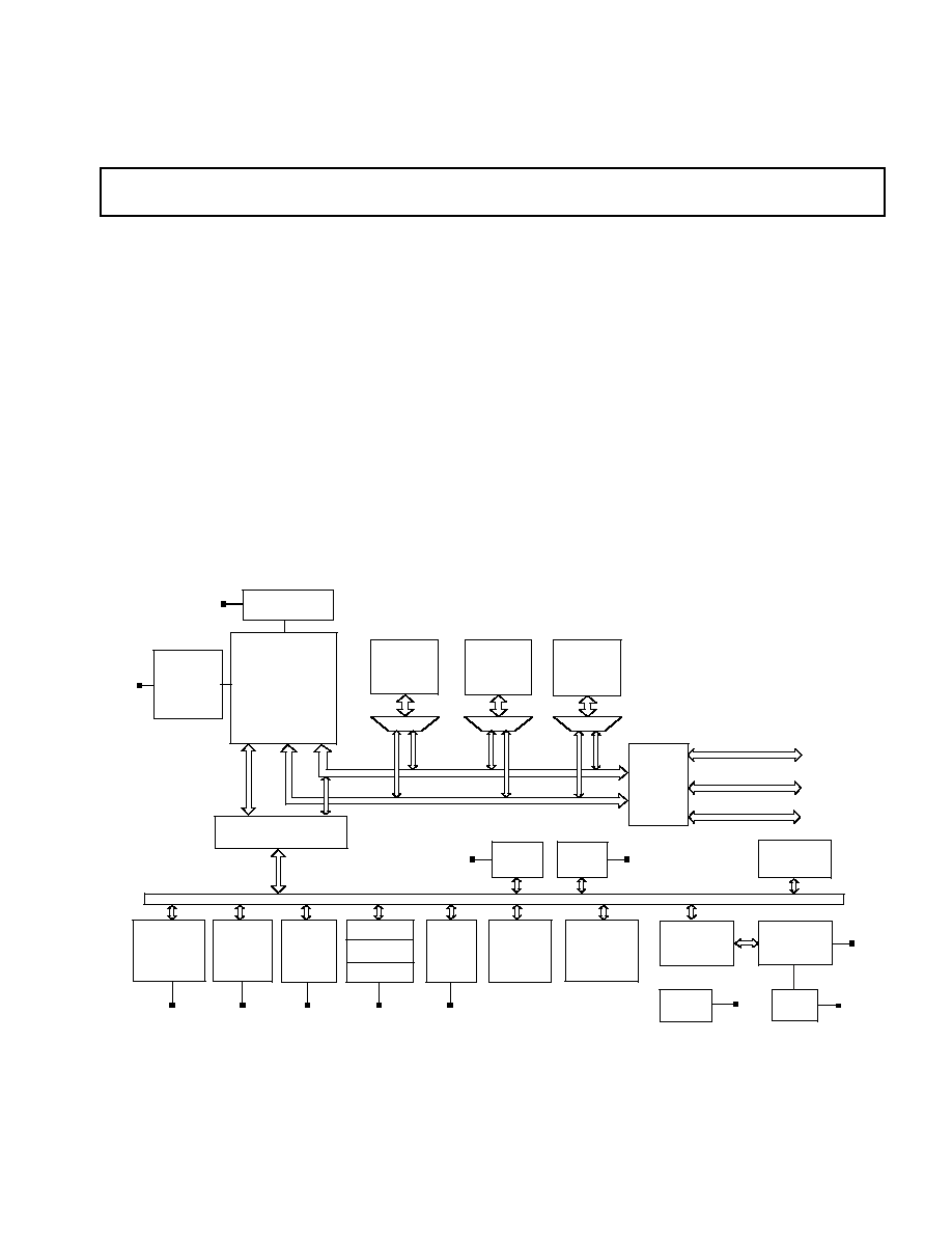
FUNCTIONAL BLOCK DIAGRAM
ADC
CONTROL
VREF
PIPELINE
FLASH ADC
CLOCK
GENERATOR/PLL
PM ADDRESS/DATA
DM ADDRESS/DATA
I/O
BUS
4K
16
DM RAM
4K
24
PM RAM
EXTERNAL
MEMORY
INTERFACE
(EMI)
TIMER 0
TIMER 1
TIMER 2
4K
24
PM ROM
ADSP-219x
DSP CORE
JTAG
TEST AND
EMULATION
ADDRESS
DATA
CONTROL
I/O REGISTERS
PWM
GENERATION
UNIT
ENCODER
INTERFACE
UNIT
(AND EET)
AUXILIARY
PWM
UNIT
FLAG
I/O
SPI
SPORT
WATCHDOG
TIMER
INTERRUPT
CONTROLLER
(ICNTL)
POR
MEMORY DMA
CONTROLLER
One Technology Way, P.O. Box 9106, Norwood, MA 02062-9106, U.S.A.
Tel:781/329-4700
www.analog.com
Fax:781/326-8703
©
2003 Analog Devices, Inc. All rights reserved.

ADSP-21990
2
REV. 0
KEY FEATURES (continued)
Integrated Power-On-Reset (POR) Generator
Flexible Power Management with Selectable Power-
Down and Idle Modes
2.5 V Internal Operation with 3.3 V I/O
Operating Temperature Range of 40ºC to +85ºC
196-Ball Mini-BGA Package
176-Lead LQFP Package
TARGET APPLICATIONS
Industrial Motor Drives
Uninterruptible Power Supplies
Optical Networking Control
Data Acquisition Systems
Test and Measurement Systems
Portable Instrumentation
TABLE OF CONTENTS
GENERAL DESCRIPTION . . . . . . . . . . . . . . . . . . . . 2
DSP Core Architecture . . . . . . . . . . . . . . . . . . . . . . . 3
Memory Architecture . . . . . . . . . . . . . . . . . . . . . . . . 4
Internal (On-Chip) Memory . . . . . . . . . . . . . . . . . . 5
External (Off-Chip) Memory . . . . . . . . . . . . . . . . . 5
External Memory Space . . . . . . . . . . . . . . . . . . . . . 5
I/O Memory Space . . . . . . . . . . . . . . . . . . . . . . . . . 5
Boot Memory Space . . . . . . . . . . . . . . . . . . . . . . . . 6
Bus Request and Bus Grant . . . . . . . . . . . . . . . . . . . . 6
DMA Controller . . . . . . . . . . . . . . . . . . . . . . . . . . . . 6
DSP Peripherals Architecture . . . . . . . . . . . . . . . . . . 6
Serial Peripheral Interface (SPI) Port . . . . . . . . . . . . . 7
DSP Serial Port (SPORT) . . . . . . . . . . . . . . . . . . . . . 7
Analog-to-Digital Conversion System . . . . . . . . . . . . 8
Voltage Reference . . . . . . . . . . . . . . . . . . . . . . . . . . . 8
PWM Generation Unit . . . . . . . . . . . . . . . . . . . . . . . 8
Auxiliary PWM Generation Unit . . . . . . . . . . . . . . . . 9
Encoder Interface Unit . . . . . . . . . . . . . . . . . . . . . . . 9
Flag I/O (FIO) Peripheral Unit . . . . . . . . . . . . . . . . 10
Watchdog Timer . . . . . . . . . . . . . . . . . . . . . . . . . . . 10
General-Purpose Timers . . . . . . . . . . . . . . . . . . . . . 10
Interrupts . . . . . . . . . . . . . . . . . . . . . . . . . . . . . . . . 10
Peripheral Interrupt Controller . . . . . . . . . . . . . . . . 11
Low Power Operation . . . . . . . . . . . . . . . . . . . . . . . 11
Idle Mode . . . . . . . . . . . . . . . . . . . . . . . . . . . . . . 11
Power-Down Core Mode . . . . . . . . . . . . . . . . . . . 11
Power-Down Core/Peripherals Mode . . . . . . . . . . 11
Power-Down All Mode . . . . . . . . . . . . . . . . . . . . 12
Clock Signals . . . . . . . . . . . . . . . . . . . . . . . . . . . . . . 12
Reset and Power-On Reset (POR) . . . . . . . . . . . . . . 12
Power Supplies . . . . . . . . . . . . . . . . . . . . . . . . . . . . 12
Booting Modes . . . . . . . . . . . . . . . . . . . . . . . . . . . . 13
Instruction Set Description . . . . . . . . . . . . . . . . . . . 13
Development Tools . . . . . . . . . . . . . . . . . . . . . . . . . 13
Designing an Emulator-Compatible DSP Board . . . 14
Additional Information . . . . . . . . . . . . . . . . . . . . . . 14
PIN FUNCTION DESCRIPTIONS . . . . . . . . . . . . . 14
SPECIFICATIONS . . . . . . . . . . . . . . . . . . . . . . . . . . 17
ABSOLUTE MAXIMUM RATINGS . . . . . . . . . . 22
ESD SENSITIVITY . . . . . . . . . . . . . . . . . . . . . . . . 22
TIMING SPECIFICATIONS . . . . . . . . . . . . . . . . 22
Clock In and Clock Out Cycle Timing . . . . . . . . . 23
Programmable Flags Cycle Timing . . . . . . . . . . . 24
Timer PWM_OUT Cycle Timing . . . . . . . . . . . . 24
External Port Write Cycle Timing . . . . . . . . . . . . 25
External Port Read Cycle Timing . . . . . . . . . . . . 26
External Port Bus Request/Grant Cycle Timing . . 27
Serial Port Timing . . . . . . . . . . . . . . . . . . . . . . . . 28
Serial Peripheral Interface Port--Master Timing . 31
Serial Peripheral Interface Port--Slave Timing . . 32
JTAG Test And Emulation Port Timing . . . . . . . 33
Power Dissipation . . . . . . . . . . . . . . . . . . . . . . . . . . 34
Test Conditions . . . . . . . . . . . . . . . . . . . . . . . . . . . 34
Output Disable Time . . . . . . . . . . . . . . . . . . . . . . 34
Output Enable Time . . . . . . . . . . . . . . . . . . . . . . 35
Example System Hold Time Calculation . . . . . . . 35
Pin Configurations . . . . . . . . . . . . . . . . . . . . . . . . 35
OUTLINE DIMENSIONS . . . . . . . . . . . . . . . . . . . . 40
ORDERING GUIDE . . . . . . . . . . . . . . . . . . . . . . . . 41
GENERAL DESCRIPTION
The ADSP-21990 is a mixed signal DSP controller based on the
ADSP-219x DSP Core, suitable for a variety of high performance
industrial motor control and signal processing applications that
require the combination of a high performance DSP and the
mixed signal integration of embedded control peripherals such
as analog-to-digital conversion.
The ADSP-21990 integrates the fixed point ADSP-219x family
base architecture with a serial port, an SPI compatible port, a
DMA controller, three programmable timers, general-purpose
Programmable Flag pins, extensive interrupt capabilities, on-
chip program and data memory spaces, and a complete set of
embedded control peripherals that permits fast motor control
and signal processing in a highly integrated environment.
The ADSP-21990 architecture is code compatible with previous
ADSP-217x based ADMCxxx products. Although the architec-
tures are compatible, the ADSP-21990, with ADSP-219x
architecture, has a number of enhancements over earlier archi-
tectures. The enhancements to computational units, data address
generators, and program sequencer make the ADSP-21990 more
flexible and easier to program than the previous ADSP-21xx
embedded DSPs.
Indirect addressing options provide addressing flexibility--
premodify with no update, pre- and post-modify by an immediate
8-bit, twos complement value and base address registers for easier
implementation of circular buffering.
The ADSP-21990 integrates 8K words of on-chip memory con-
figured as 4K words (24-bit) of program RAM, and 4K words
(16-bit) of data RAM.
Fabricated in a high speed, low power, CMOS process, the
ADSP-21990 operates with a 6.25 ns instruction cycle time for
a 160 MHz CCLK and with a 6.67 ns instruction cycle time for
a 150 MHz CCLK.

3
REV. 0
ADSP-21990
The flexible architecture and comprehensive instruction set of
the ADSP-21990 support multiple operations in parallel. For
example, in one processor cycle, the ADSP-21990 can:
· Generate an address for the next instruction fetch.
· Fetch the next instruction.
· Perform one or two data moves.
· Update one or two data address pointers.
· Perform a computational operation.
These operations take place while the processor continues to:
· Receive and transmit data through the serial port.
· Receive or transmit data over the SPI port.
· Access external memory through the external memory
interface.
· Decrement the timers.
· Operate the embedded control peripherals (ADC, PWM,
EIU, etc.).
DSP Core Architecture
· 6.25 ns instruction cycle time (internal), for up to
160 MIPS sustained performance (6.67 ns instruction
cycle time for 150 MIPS sustained performance).
· ADSP-218x family code compatible with the same easy
to use algebraic syntax.
· Single cycle instruction execution.
· Up to 1M words of addressable memory space with
twenty four bits of addressing width.
· Dual purpose program memory for both instruction and
data storage.
· Fully transparent instruction cache allows dual operand
fetches in every instruction cycle.
· Unified memory space permits flexible address genera-
tion, using two independent DAG units.
· Independent ALU, multiplier/accumulator, and barrel
shifter computational units with dual 40-bit
accumulators.
· Single cycle context switch between two sets of computa-
tional and DAG registers.
· Parallel execution of computation and memory
instructions.
· Pipelined architecture supports efficient code execution
at speeds up to 160 MIPS.
· Register file computations with all nonconditional, non-
parallel computational instructions.
· Powerful program sequencer provides zero overhead
looping and conditional instruction execution.
· Architectural enhancements for compiled C code
efficiency.
· Architecture enhancements beyond ADSP-218x family
are supported with instruction set extensions for added
registers, ports, and peripherals.
The clock generator module of the ADSP-21990 includes clock
control logic that allows the user to select and change the main
clock frequency. The module generates two output clocks: the
DSP core clock, CCLK; and the peripheral clock, HCLK.
CCLK can sustain clock values of up to 160 MHz, while HCLK
can be equal to CCLK or CCLK/2 for values up to a maximum
80 MHz peripheral clock at the 160 MHz CCLK rate.
The ADSP-21990 instruction set provides flexible data moves
and multifunction (one or two data moves with a computation)
instructions. Every single word instruction can be executed in a
single processor cycle. The ADSP-21990 assembly language uses
an algebraic syntax for ease of coding and readability. A compre-
hensive set of development tools supports program development.
The block diagram
Figure 1
shows the architecture of the
embedded ADSP-219x core. It contains three independent com-
putational units: the ALU, the multiplier/accumulator (MAC),
and the shifter. The computational units process 16-bit data from
the register file and have provisions to support multiprecision
computations. The ALU performs a standard set of arithmetic
and logic operations; division primitives are also supported. The
MAC performs single cycle multiply, multiply/add, and multi-
ply/subtract operations. The MAC has two 40-bit accumulators,
which help with overflow. The shifter performs logical and arith-
metic shifts, normalization, denormalization, and derive
exponent operations. The shifter can be used to efficiently
implement numeric format control, including multiword and
block floating point representations.
Register usage rules influence placement of input and results
within the computational units. For most operations, the com-
putational unit data registers act as a data register file, permitting
any input or result register to provide input to any unit for a
computation. For feedback operations, the computational units
let the output (result) of any unit be input to any unit on the next
cycle. For conditional or multifunction instructions, there are
restrictions on which data registers may provide inputs or receive
results from each computational unit. For more information, see
the ADSP-219x DSP Instruction Set Reference.
A powerful program sequencer controls the flow of instruction
execution. The sequencer supports conditional jumps, subrou-
tine calls, and low interrupt overhead. With internal loop
counters and loop stacks, the ADSP-21990 executes looped code
with zero overhead; no explicit jump instructions are required to
maintain loops.
Two data address generators (DAGs) provide addresses for
simultaneous dual operand fetches (from data memory and
program memory). Each DAG maintains and updates four 16-
bit address pointers. Whenever the pointer is used to access data
(indirect addressing), it is pre- or post-modified by the value of
one of four possible modify registers. A length value and base
address may be associated with each pointer to implement
automatic modulo addressing for circular buffers. Page registers
in the DAGs allow circular addressing within 64K word bound-
aries of each of the 256 memory pages, but these buffers may not
cross page boundaries. Secondary registers duplicate all the
primary registers in the DAGs; switching between primary and
secondary registers provides a fast context switch.
ADSP-21990
4
REV. 0
Efficient data transfer in the core is achieved with the use of
internal buses:
· Program Memory Address (PMA) Bus
· Program Memory Data (PMD) Bus
· Data Memory Address (DMA) Bus
· Data Memory Data (DMD) Bus
· Direct Memory Access Address Bus
· Direct Memory Access Data Bus
The two address buses (PMA and DMA) share a single external
address bus, allowing memory to be expanded off-chip, and the
two data buses (PMD and DMD) share a single external data
bus. Boot memory space and I/O memory space also share the
external buses.
Program memory can store both instructions and data, permit-
ting the ADSP-21990 to fetch two operands in a single cycle, one
from program memory and one from data memory. The dual
memory buses also let the embedded ADSP-219x core fetch an
operand from data memory and the next instruction from
program memory in a single cycle.
Memory Architecture
The ADSP-21990 provides 8K words of on-chip SRAM
memory. This memory is divided into two blocks: a 4K
× 24-bit
(block 0) and a 4K
× 16-bit (block 1). In addition, the
ADSP-21990 provides a 4K
× 24-bit block of program memory
boot ROM (that is reserved by ADI for boot load routines). The
memory map of the ADSP-21990 is illustrated in Figure 2.
As shown in Figure 2, the two internal memory RAM blocks
reside in memory page 0. The entire DSP memory map consists
of 256 pages (pages 0 to 255), and each page is 64K words long.
External memory space consists of four memory banks
(banks30) and supports a wide variety of memory devices. Each
bank is selectable using unique memory select lines (
MS30) and
has configurable page boundaries, wait states, and wait state
modes. The 4K words of on-chip boot ROM populates the top
of page 255, while the remaining 254 pages are addressable off-
chip. I/O memory pages differ from external memory in that they
are 1K word long, and the external I/O pages have their own select
pin (
IOMS). Pages 310 of I/O memory space reside on-chip and
contain the configuration registers for the peripherals. Both the
ADSP-219x core and DMA capable peripherals can access the
the entire memory map of the DSP.
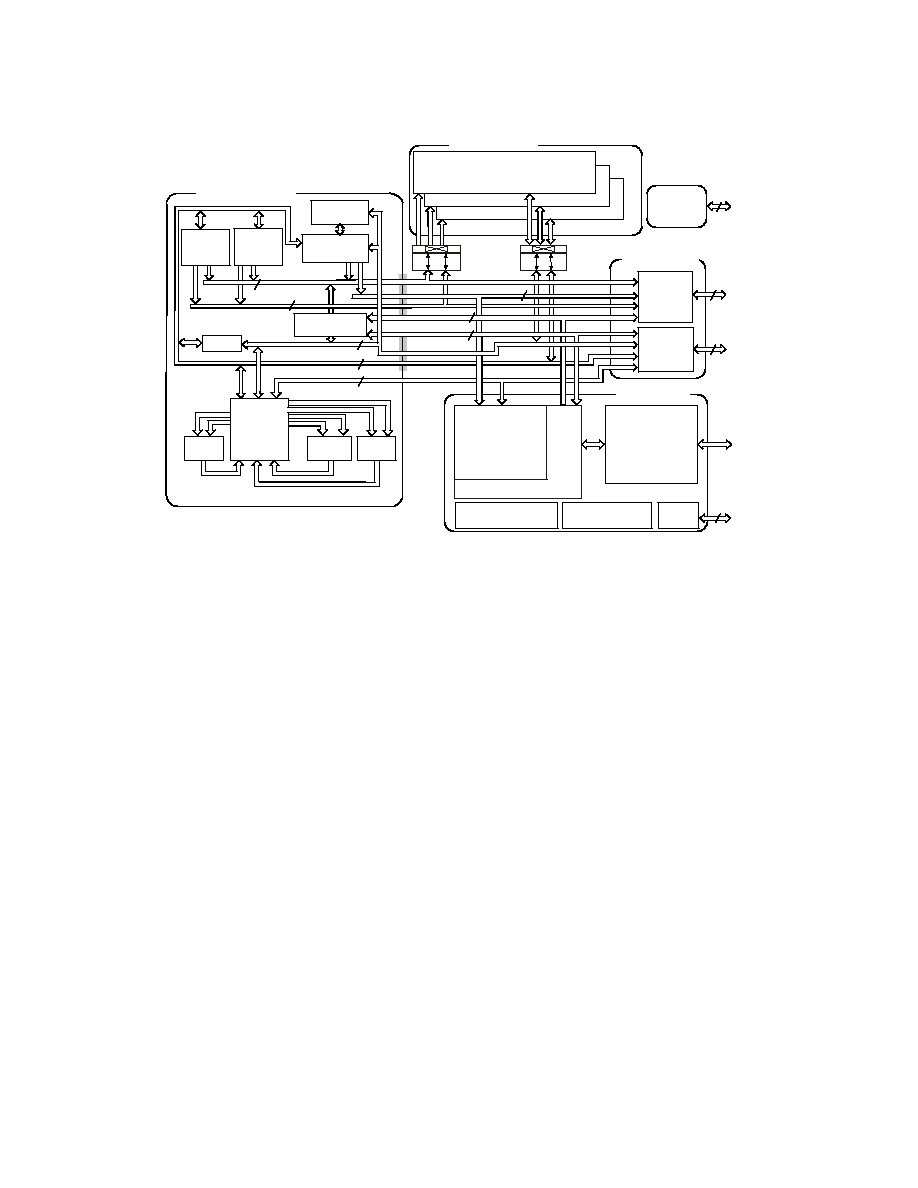
Figure 1. Block Diagram
DATA
ADDRESS
B
L
O
C
K
2
SYSTEM INTERRUPT
CONTROLLER
I/O DATA
I/O REGISTERS
(MEMORY-MAPPED)
CONTROL
STATUS
BUFFERS
I/O PROCESSOR
CACHE
64
24-BIT
JTAG
TEST AND
EMULATION
6
ADDR BUS
MUX
DATA BUS
MUX
16
20
PM ADDRESS BUS
DM ADDRESS BUS
PM DATA BUS
DM DATA BUS
PX
24
16
ADSP-219x DSP CORE
PROGRAM
SEQUENCER
DATA
REGISTER
FILE
MULT
BARREL
SHIFTER
ALU
DMA CONTROLLER
INPUT
REGISTERS
RESULT
REGISTERS
16
16-BIT
DAG1
4
4
16
DAG2
4
4
16
INTERNAL MEMORY
24
24
ADDRESS
B
L
O
C
K
1
DATA
DATA
ADDRESS
B
L
O
C
K
0
24 BIT
16 BIT
16 BIT
FOUR INDEPENDENT BLOCKS
PROGRAMMABLE
FLAGS (16)
TIMERS
(3)
3
DMA CONNECT
DMA ADDRESS
EXTERNAL PORT
18
I/O ADDRESS
24
16
24
DMA DATA
EMBEDDED
CONTROL
PERIPHERALS
AND
COMMUNICATIONS
PORTS
5
REV. 0
ADSP-21990
NOTE: The physical external memory addresses are limited by
20 address lines, and are determined by the external data width
and packing of the external memory space. The Strobe signals
(
MS3-0) can be programmed to allow the user to change starting
page addresses at run time.
Internal (On-Chip) Memory
The ADSP-21990 unified program and data memory space
consists of 16M locations that are accessible through two 24-bit
address buses, the PMA and DMA buses. The DSP uses slightly
different mechanisms to generate a 24-bit address for each bus.
The DSP has three functions that support access to the full
memory map.
· The DAGs generate 24-bit addresses for data fetches from
the entire DSP memory address range. Because DAG
index (address) registers are 16 bits wide and hold the
lower 16 bits of the address, each of the DAGs has its own
8-bit page register (DMPGx) to hold the most significant
eight address bits. Before a DAG generates an address,
the program must set the DAG DMPGx register to the
appropriate memory page. The DMPG1 register is also
used as a page register when accessing external memory.
The program must set DMPG1 accordingly, when
accessing data variables in external memory. A "C"
program macro is provided for setting this register.
· The program sequencer generates the addresses for
instruction fetches. For relative addressing instructions,
the program sequencer bases addresses for relative jumps,
calls, and loops on the 24-bit Program Counter (PC). In
direct addressing instructions (two word instructions),
the instruction provides an immediate 24-bit address
value. The PC allows linear addressing of the full 24-bit
address range.
· For indirect jumps and calls that use a 16-bit DAG
address register for part of the branch address, the
Program Sequencer relies on an 8-bit Indirect Jump page
(IJPG) register to supply the most significant eight
address bits. Before a cross page jump or call, the program
must set the program sequencer IJPG register to the
appropriate memory page.
The ADSP-21990 has 4K word of on-chip ROM that holds boot
routines. The DSP starts executing instructions from the on-chip
boot ROM, which starts the boot process.
See Booting Modes
on Page 13.
The on-chip boot ROM is located on Page 255 in
the DSP memory space map, starting at address 0xFF0000.
External (Off-Chip) Memory
Each of the ADSP-21990 off-chip memory spaces has a separate
control register, so applications can configure unique access
parameters for each space. The access parameters include read
and write wait counts, wait state completion mode, I/O clock
divide ratio, write hold time extension, strobe polarity, and data
bus width. The core clock and peripheral clock ratios influence
the external memory access strobe widths.
See Clock Signals on
Page 12.
The off-chip memory spaces are:
· External memory space (MS30 pins)
· I/O memory space (IOMS pin)
· Boot memory space (BMS pin)
All of the above off-chip memory spaces are accessible through
the External Port, which can be configured for 8-bit or 16-bit
data widths.
External Memory Space
External memory space consists of four memory banks. These
banks can contain a configurable number of 64 K word pages. At
reset, the page boundaries for external memory have Bank0 con-
taining pages 1 to 63, Bank1 containing pages 64 to 127, Bank2
containing pages 128 to 191, and Bank3 containing pages 192 to
254. The
MS3-0 memory bank pins select Banks 3-0, respec-
tively. Both the ADSP-219x core and DMA capable peripherals
can access the DSP external memory space.
All accesses to external memory are managed by the External
Memory Interface Unit (EMI).
I/O Memory Space
The ADSP-21990 supports an additional external memory
called I/O memory space. The IO space consists of 256 pages,
each containing 1024 addresses. This space is designed to
support simple connections to peripherals (such as data convert-
ers and external registers) or to bus interface ASIC data registers.
The first 32K addresses (IO pages 0 to 31) are reserved for
on-chip peripherals. The upper 224K addresses (IO pages 32 to
255) are available for external peripheral devices. External I/O
pages have their own select pin (
IOMS). The DSP instruction
set provides instructions for accessing I/O space.
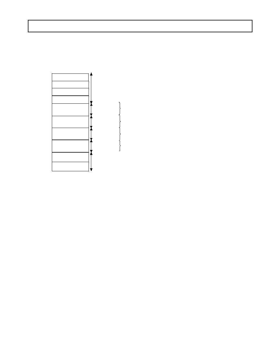
Figure 2. Core Memory Map at Reset
0x00 0000
0x00 0FFF
0x00 7FFF
0x00 8FFF
0x01 0000
0x40 0000
0x80 0000
0xC0 0000
0xFF 0000
0xFF 1000
0xFF FFFF
0x00 8000
0x00 1000
0x00 9000
0x00 FFFF
0xFF 0FFF
PAGE 0 (64K) ON-CHIP
(0 WAIT STATE)
EXTERNAL MEMORY
(4M 64K)
PAGES 1 TO 63
BANK 0 (OFF-CHIP)
MS0
PAGE 255
(ON-CHIP)
EXTERNAL MEMORY
EXTERNAL MEMORY
PAGES 64 TO 127
BANK 1 (OFF-CHIP)
PAGES 128 TO 191
BANK 2 (OFF-CHIP)
PAGES 192 TO 254
BANK 0 (OFF-CHIP)
MS1
MS2
MS3
EXTERNAL MEMORY
(4M 64K)
BLOCK 0: 4K
24-BIT RAM
RESERVED (28K)
RESERVED (28K)
BLOCK 1: 4K
16-BIT RAM
BLOCK 2: 4K
24-BIT
PM ROM
UNUSED ON-CHIP
MEMORY (60K)
ADSP-21990
6
REV. 0
Boot Memory Space
Boot memory space consists of one off-chip bank with 254 pages.
The
BMS memory bank pin selects boot memory space. Both
the ADSP-219x core and DMA capable peripherals can access
the DSP off-chip boot memory space. After reset, the DSP always
starts executing instructions from the on-chip boot ROM.
Bus Request and Bus Grant
The ADSP-21990 can relinquish control of the data and address
buses to an external device. When the external device requires
access to the bus, it asserts the bus request (
BR) signal. The (BR)
signal is arbitrated with core and peripheral requests. External
Bus requests have the lowest priority. If no other internal request
is pending, the external bus request will be granted. Due to syn-
chronizer and arbitration delays, bus grants will be provided with
a minimum of three peripheral clock delays. The ADSP-21990
will respond to the bus grant by:
· Three-stating the data and address buses and the MS30,
BMS, IOMS, RD, and WR output drivers.
· Asserting the bus grant (BG) signal.
The ADSP-21990 will halt program execution if the bus is
granted to an external device and an instruction fetch or data
read/write request is made to external general-purpose or periph-
eral memory spaces. If an instruction requires two external
memory read accesses, the bus will not be granted between the
two accesses. If an instruction requires an external memory read
and an external memory write access, the bus may be granted
between the two accesses. The external memory interface can be
configured so that the core will have exclusive use of the interface.
DMA and Bus Requests will be granted. When the external
device releases
BR, the DSP releases BG and continues program
execution from the point at which it stopped.
The bus request feature operates at all times, even while the DSP
is booting and
RESET is active.
The ADSP-21990 asserts the
BGH pin when it is ready to start
another external port access, but is held off because the bus was
previously granted. This mechanism can be extended to define
more complex arbitration protocols for implementing more
elaborate multimaster systems.
DMA Controller
The ADSP-21990 has a DMA controller that supports
automated data transfers with minimal overhead for the DSP
core. Cycle stealing DMA transfers can occur between the
ADSP-21990 internal memory and any of its DMA capable
peripherals. Additionally, DMA transfers can be accomplished
between any of the DMA capable peripherals and external
devices connected to the external memory interface. DMA
capable peripherals include the SPORT and SPI ports, and ADC
Control module. Each individual DMA capable peripheral has a
dedicated DMA channel. To describe each DMA sequence, the
DMA controller uses a set of parameters--called a DMA descrip-
tor. When successive DMA sequences are needed, these DMA
descriptors can be linked or chained together, so the completion
of one DMA sequence auto initiates and starts the next sequence.
DMA sequences do not contend for bus access with the DSP
core, instead DMAs "steal" cycles to access memory.
All DMA transfers use the DMA bus shown in
Figure 1 on
Page 4
. Because all of the peripherals use the same bus, arbitra-
tion for DMA bus access is needed. The arbitration for DMA bus
access appears in
Table 1
.
DSP Peripherals Architecture
The ADSP-21990 contains a number of special purpose,
embedded control peripherals, which can be seen in the Func-
tional Block Diagram on Page 1. The ADSP-21990 contains a
high performance, 8-channel, 14-bit ADC system with dual
channel simultaneous sampling ability across four pairs of inputs.
An internal precision voltage reference is also available as part of
the ADC system. In addition, a 3-phase, 16-bit, center based
PWM generation unit can be used to produce high accuracy
PWM signals with minimal processor overhead.
The ADSP-21990 also contains a flexible incremental encoder
interface unit for position sensor feedback; two adjustable
frequency auxiliary PWM outputs, 16 lines of digital I/O; a
16-bit watchdog timer; three general-purpose timers, and an
interrupt controller that manages all peripheral interrupts.
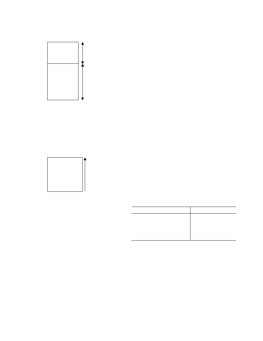
Figure 3. I/O Memory Map
Figure 4. Boot Memory Map
ON-CHIP
PERIPHERALS
16-BITS
OFF-CHIP
PERIPHERALS
16-BITS
PAGES 0 TO 31
1024 WORDS/PAGE
2 PERIPHERALS/PAGE
0x00::0x000
0x20::0x000
0xFF::0x3FF
0x1F::0x3FF
PAGES 32 TO 255
1024 WORDS/PAGE
PAGES 1 TO 254
64K WORDS/PAGE
0x01 0000
0xFE 0000
OFF-CHIP
BOOT MEMORY
16-BITS
Table 1. I/O Bus Arbitration Priority
DMA Bus Master
Arbitration Priority
SPORT Receive DMA
0--Highest
SPORT Transmit DMA
1
ADC Control DMA
2
SPI Receive/Transmit DMA
3
Memory DMA
4--Lowest

7
REV. 0
ADSP-21990
Finally, the ADSP-21990 contains an integrated power-on-reset
(POR) circuit that can be used to generate the required reset
signal for the device on power-on.
The ADSP-21990 has an external memory interface that is
shared by the DSP core, the DMA controller, and DMA capable
peripherals, which include the ADC, SPORT, and SPI commu-
nication ports. The external port consists of a 16-bit data bus, a
20-bit address bus, and control signals. The data bus is config-
urable to provide an 8- or 16-bit interface to external memory.
Support for word packing lets the DSP access 16- or 24-bit words
from external memory regardless of the external data bus width.
The memory DMA controller lets the ADSP-21990 move data
and instructions from between memory spaces: internal-to-
external, internal-to-internal, and external-to-external. On-chip
peripherals can also use this controller for DMA transfers.
The embedded ADSP-219x core can respond to up to seventeen
interrupts at any given time: three internal (stack, emulator
kernel, and power down), two external (emulator and reset), and
twelve user defined (peripherals) interrupts. Programmers assign
each of the 32 peripheral interrupt requests to one of the 12 user
defined interrupts. These assignments determine the priority of
each peripheral for interrupt service.
The following sections provide a functional overview of the
ADSP-21990 peripherals.
Serial Peripheral Interface (SPI) Port
The Serial Peripheral Interface (SPI) Port provides functionality
for a generic configurable serial port interface based on the SPI
standard, which enables the DSP to communicate with multiple
SPI compatible devices. Key features of the SPI port are:
· Interface to host microcontroller or serial EEPROM
· Master or slave operation (3-wire interface MISO, MOSI,
SCK)
· Data rates to HCLK 4 (16-bit baud rate selector)
· 8- or 16-bit transfer
· Programmable clock phase and polarity
· Broadcast Mode 1 master, multiple slaves
· DMA capability and dedicated interrupts
· PF0 can be used as Slave Select input line
· PF1PF7 can be used as external Slave Select output
SPI is a 3-wire interface consisting of 2 data pins (MOSI and
MISO), one clock pin (SCK), and a single Slave Select input
(
SPISS) that is multiplexed with the PF0 Flag IO line and seven
Slave Select outputs (SPISEL1 to SPISEL7) that are multiplexed
with the PF1 to PF7 Flag IO lines. The
SPISS input is used to
select the ADSP-21990 as a slave to an external master. The
SPISEL1 to SPISEL7 outputs can be used by the ADSP-21990
(acting as a master) to select/enable up to seven external slaves
in a multidevice SPI configuration. In a multimaster or a multi-
device configuration, all MOSI pins are tied together, all MISO
pins are tied together, and all SCK pins are tied together.
During transfers, the SPI port simultaneously transmits and
receives by serially shifting data in and out on the serial data line.
The serial clock line synchronizes the shifting and sampling of
data on the serial data line.
In master mode, the DSP core performs the following sequence
to set up and initiate SPI transfers:
1. Enables and configures the SPI port operation (data size,
and transfer format).
2. Selects the target SPI slave with the SPISELx output pin
(reconfigured Programmable Flag pin).
3. Defines one or more DMA descriptors in Page 0 of I/O
memory space (optional in DMA mode only).
4. Enables the SPI DMA engine and specifies transfer
direction (optional in DMA mode only).
5. In non DMA mode only, reads or writes the SPI port
receive or transmit data buffer.
The SCK line generates the programmed clock pulses for simul-
taneously shifting data out on MOSI and shifting data in on
MISO. In DMA mode only, transfers continue until the SPI
DMA word count transitions from 1 to 0.
In slave mode, the DSP core performs the following sequence to
set up the SPI port to receive data from a master transmitter:
1. Enables and configures the SPI slave port to match the
operation parameters set up on the master (data size and
transfer format) SPI transmitter.
2. Defines and generates a receive DMA descriptor in
Page 0 of memory space to interrupt at the end of the
data transfer (optional in DMA mode only).
3. Enables the SPI DMA engine for a receive access
(optional in DMA mode only).
4. Starts receiving the data on the appropriate SCK edges
after receiving an SPI chip select on the
SPISS input pin
(reconfigured Programmable Flag pin) from a master.
In DMA mode only, reception continues until the SPI DMA
word count transitions from 1 to 0. The DSP core could
continue, by queuing up the next DMA descriptor.
Slave mode transmit operation is similar, except that the DSP
core specifies the data buffer in memory space from which to
transmit data, generates and relinquishes control of the transmit
DMA descriptor, and begins filling the SPI port data buffer. If
the SPI controller is not ready on time to transmit, it can transmit
a "zero" word.
DSP Serial Port (SPORT)
The ADSP-21990 incorporates a complete synchronous serial
port (SPORT) for serial and multiprocessor communications.
The SPORT supports the following features:
· Bidirectional: the SPORT has independent transmit and
receive sections.
· Double buffered: the SPORT section (both receive and
transmit) has a data register for transferring data words
to and from other parts of the processor and a register for
shifting data in or out. The double buffering provides
additional time to service the SPORT.

ADSP-21990
8
REV. 0
· Clocking: the SPORT can use an external serial clock or
generate its own in a wide range of frequencies down to
0 Hz.
· Word length: each SPORT section supports serial data
word lengths from three to sixteen bits that can be trans-
ferred either MSB first or LSB first.
· Framing: each SPORT section (receive and transmit) can
operate with or without frame synchronization signals for
each data-word; with internally generated or externally
generated frame signals; with active high or active low
frame signals; with either of two pulsewidths and frame
signal timing.
· Companding in hardware: each SPORT section can
perform A law and µ law companding according to
CCITT recommendation G.711.
· Direct Memory Access with single cycle overhead: using
the built-in DMA master, the SPORT can automatically
receive and/or transmit multiple memory buffers of data
with an overhead of only one DSP cycle per data-word.
The on-chip DSP via a linked list of memory space
resident DMA descriptor blocks can configure transfers
between the SPORT and memory space. This chained list
can be dynamically allocated and updated.
· Interrupts: each SPORT section (receive and transmit)
generates an interrupt upon completing a data-word
transfer, or after transferring an entire buffer or buffers if
DMA is used.
· Multichannel capability: The SPORT can receive and
transmit data selectively from channels of a serial bit
stream that is time division multiplexed into up to 128
channels. This is especially useful for T1 interfaces or as
a network communication scheme for multiple proces-
sors. The SPORTs also support T1 and E1 carrier
systems.
· Each SPORT channel (Tx and Rx) supports a DMA
buffer of up to eight, 16-bit transfers.
· The SPORT operates at a frequency of up to one-half the
clock frequency of the HCLK.
· The SPORT is capable of UART software emulation.
Analog-to-Digital Conversion System
The ADSP-21990 contains a fast, high accuracy, multiple input
analog-to-digital conversion system with simultaneous sampling
capabilities. This A/D conversion system permits the fast,
accurate conversion of analog signals needed in high performance
embedded systems. Key features of the ADC system are:
· 14-bit Pipeline (6-Stage Pipeline) Flash Analog-to-
Digital Converter
· 8 dedicated analog inputs
· Dual channel simultaneous sampling capability
· Programmable ADC clock rate to maximum of HCLK 4
· First channel ADC data valid approximately 375 ns after
CONVST (at 20 MSPS)
· All 8 inputs converted in approximately 725 ns (at
20 MSPS)
· 2.0 V peak-to-peak input voltage range
· Multiple convert start sources
· Internal or external Voltage Reference
· Out of range detection
· DMA capable transfers from ADC to memory
The ADC system is based on a pipeline flash converter core, and
contains dual input sample-and-hold amplifiers so that simulta-
neous sampling of two input signals is supported. The ADC
system provides an analog input voltage range of 2.0 Vp-p and
provides 14-bit performance with a clock rate of up to HCLK 4.
The ADC system can be programmed to operate at a clock rate
that is programmable from HCLK 4 to HCLK 30, to a
maximum of 20 MHz (at 160 MHz CCLK rate).
The ADC input structure supports 8 independent analog inputs;
four of which are multiplexed into one sample-and-hold amplifier
(A_SHA) and 4 of which are multiplexed into the other sample-
and-hold amplifier (B_SHA).
At the 20 MHz sampling rate, the first data value is valid approx-
imately 375 ns after the Convert Start command. All 8 channels
are converted in approximately 725 ns.
The core of the ADSP-21990 provides 14-bit data such that the
stored data values in the ADC data registers are 14 bits wide.
Voltage Reference
The ADSP-21990 contains an onboard band gap reference that
can be used to provide a precise 1.0 V output for use by the A/D
system and externally on the VREF pin for biasing and level
shifting functions. Additionally, the ADSP-21990 may be con-
figured to operate with an external reference applied to the VREF
pin, if required.
PWM Generation Unit
Key features of the 3-phase PWM generation unit are:
· 16-bit, center based PWM generation unit
· Programmable PWM pulsewidth, with resolutions to
12.5 ns (at 80 MHz HCLK rate)
· Single/double update modes
· Programmable dead time and switching frequency
· Twos complement implementation permits smooth tran-
sition into full ON and full OFF states
· Possibility to synchronize the PWM generation to an
external synchronization
· Special provisions for BDCM Operation (crossover and
output enable functions)
· Wide Variety of special switched reluctance (SR)
operating modes
· Output polarity and clock gating control
· Dedicated asynchronous PWM shutdown signal
· Multiple shutdown sources, independently for each unit

9
REV. 0
ADSP-21990
The ADSP-21990 integrates a flexible and programmable,
3-phase PWM waveform generator that can be programmed to
generate the required switching patterns to drive a 3-phase
voltage source inverter for ac induction (ACIM) or permanent
magnet synchronous (PMSM) motor control. In addition, the
PWM block contains special functions that considerably simplify
the generation of the required PWM switching patterns for
control of the electronically commutated motor (ECM) or
brushless dc motor (BDCM). Tying a dedicated pin,
PWMSR,
to GND, enables a special mode, for switched reluctance motors
(SRM).
The six PWM output signals consist of three high side drive pins
(AH, BH, and CH) and three low side drive signals pins (AL,
BL, and CL). The polarity of the generated PWM signals may
be set via hardware by the PWMPOL input pin, so that either
active HI or active LO PWM patterns can be produced.
The switching frequency of the generated PWM patterns is pro-
grammable using the 16-bit PWMTM register. The PWM
generator is capable of operating in two distinct modes, single
update mode or double update mode. In single update mode the
duty cycle values are programmable only once per PWM period,
so that the resultant PWM patterns are symmetrical about the
midpoint of the PWM period. In the double update mode, a
second updating of the PWM registers is implemented at the
midpoint of the PWM period. In this mode, it is possible to
produce asymmetrical PWM patterns. that produce lower
harmonic distortion in 3-phase PWM inverters.
Auxiliary PWM Generation Unit
Key features of the auxiliary PWM generation unit are:
· 16-bit, programmable frequency, programmable duty
cycle PWM outputs
· Independent or offset operating modes
· Double buffered control of duty cycle and period registers
· Separate auxiliary PWM synchronization signal and asso-
ciated interrupt (can be used to trigger ADC Convert
Start)
· Separate auxiliary PWM shutdown signal (AUXTRIP)
The ADSP-21990 integrates a 2-channel, 16-bit, auxiliary PWM
output unit that can be programmed with variable frequency,
variable duty cycle values and may operate in two different
modes, independent mode or offset mode. In independent mode,
the two auxiliary PWM generators are completely independent
and separate switching frequencies and duty cycles may be pro-
grammed for each auxiliary PWM output. In offset mode the
switching frequency of the two signals on the AUX0 and AUX1
pins is identical. Bit 4 of the AUXCTRL register places the
auxiliary PWM channel pair in independent or offset mode.
The auxiliary PWM generation unit provides two chip output
pins, AUX0 and AUX1 (on which the switching signals appear)
and one chip input pin,
AUXTRIP, which can be used to shut
down the switching signals--for example, in a fault condition.
Encoder Interface Unit
The ADSP-21990 incorporates a powerful encoder interface
block to incremental shaft encoders that are often used for
position feedback in high performance motion control systems.
· Quadrature rates to 53 MHz (at 80 MHz HCLK rate)
· Programmable filtering of all encoder input signals
· 32-bit encoder counter
· Variety of hardware and software reset modes
· Two registration inputs to latch EIU count value with
corresponding registration interrupt
· Status of A/B signals latched with reading of EIU count
value
· Alternative frequency and direction mode
· Single north marker mode
· Count error monitor function with dedicated error
interrupt
· Dedicated 16-bit loop timer with dedicated interrupt
· Companion encoder event (1/T) timer unit
The encoder interface unit (EIU) includes a 32-bit quadrature
up/down counter, programmable input noise filtering of the
encoder input signals and the zero markers, and has four
dedicated chip pins. The quadrature encoder signals are applied
at the EIA and EIB pins. Alternatively, a frequency and direction
set of inputs may be applied to the EIA and EIB pins. In addition,
two north marker/strobe inputs are provided on pins EIZ and
EIS. These inputs may be used to latch the contents of the
encoder quadrature counter into dedicated registers,
EIZLATCH and EISLATCH, on the occurrence of external
events at the EIZ and EIS pins. These events may be programmed
to be either rising edge only (latch event) or rising edge if the
encoder is moving in the forward direction and falling edge if the
encoder is moving in the reverse direction (software latched north
marker functionality).
The encoder interface unit incorporates programmable noise
filtering on the four encoder inputs to prevent spurious noise
pulses from adversely affecting the operation of the quadrature
counter. The encoder interface unit operates at a clock frequency
equal to the HCLK rate. The encoder interface unit operates
correctly with encoder signals at frequencies of up to 13.25 MHz
at the 80 MHz HCLK rate, corresponding to a maximum
quadrature frequency of 53 MHz (assuming an ideal quadrature
relationship between the input EIA and EIB signals).
The EIU may be programmed to use the north marker on EIZ
to reset the quadrature encoder in hardware, if required.
Alternatively, the north marker can be ignored, and the encoder
quadrature counter is reset according to the contents of a
maximum count register, EIUMAXCNT. There is also a "single
north marker" mode available in which the encoder quadrature
counter is reset only on the first north marker pulse.

ADSP-21990
10
REV. 0
The encoder interface unit can also be made to implement some
error checking functions. If an encoder count error is detected
(due to a disconnected encoder line, for example), a status bit in
the EIUSTAT register is set, and an EIU count error interrupt is
generated.
The encoder interface unit of the ADSP-21990 contains a 16-bit
loop timer that consists of a timer register, period register and
scale register so that it can be programmed to time out and reload
at appropriate intervals. When this loop timer times out, an EIU
loop timer timeout interrupt is generated. This interrupt could
be used to control the timing of speed and position control loops
in high performance drives.
The encoder interface unit also includes a high performance
encoder event timer (EET) block that permits the accurate timing
of successive events of the encoder inputs. The EET can be pro-
grammed to time the duration between up to 255 encoder pulses
and can be used to enhance velocity estimation, particularly at
low speeds of rotation.
Flag I/O (FIO) Peripheral Unit
The FIO module is a generic parallel I/O interface that supports
sixteen bidirectional multifunction flags or general-purpose
digital I/O signals (PF150).
All sixteen FLAG bits can be individually configured as an input
or output based on the content of the direction (DIR) register,
and can also be used as an interrupt source for one of two FIO
interrupts. When configured as input, the input signal can be
programmed to set the FLAG on either a level (level sensitive
input/interrupt) or an edge (edge sensitive input/interrupt).
The FIO module can also be used to generate an asynchronous
unregistered wake-up signal FIO_WAKEUP for DSP core wake
up after power-down.
The FIO Lines, PF71 can also be configured as external slave
select outputs for the SPI communications port, while PF0 can
be configured to act as a slave select input.
The FIO Lines can be configured to act as a PWM shutdown
source for the 3-phase PWM generation unit of the
ADSP-21990.
Watchdog Timer
The ADSP-21990 integrates a watchdog timer that can be used
as a protection mechanism against unintentional software events.
It can be used to cause a complete DSP and peripheral reset in
such an event. The watchdog timer consists of a 16-bit timer that
is clocked at the external clock rate (CLKIN or crystal input
frequency).
In order to prevent an unwanted timeout or reset, it is necessary
to periodically write to the watchdog timer register. During
abnormal system operation, the watchdog count will eventually
decrement to 0 and a watchdog timeout will occur. In the system,
the watchdog timeout will cause a full reset of the DSP core and
peripherals.
General-Purpose Timers
The ADSP-21990 contains a general-purpose timer unit that
contains three identical 32-bit timers. The three programmable
interval timers (Timer0, Timer1, and Timer2) generate periodic
interrupts. Each timer can be independently set to operate in one
of three modes:
· Pulse Waveform Generation (PWM_OUT) mode
· Pulsewidth Count/Capture (WDTH_CAP) mode
· External Event Watchdog (EXT_CLK) mode
Each Timer has one bidirectional chip pin, TMR2-0. For each
timer, the associated pin is configured as an output pin in
PWM_OUT Mode and as an input pin in WDTH_CAP and
EXT_CLK Modes.
Interrupts
The interrupt controller lets the DSP respond to 17 interrupts
with minimum overhead. The DSP core implements an interrupt
priority scheme as shown in
Table 2
. Applications can use the
unassigned slots for software and peripheral interrupts. The
Peripheral Interrupt Controller is used to assign the various
peripheral interrupts to the 12 user assignable interrupts of the
DSP core.
There is no assigned priority for the peripheral interrupts after
reset. To assign the peripheral interrupts a different priority,
applications write the new priority to their corresponding control
bits (determined by their ID) in the Interrupt Priority Control
register.
Interrupt routines can either be nested with higher priority inter-
rupts taking precedence or processed sequentially. Interrupts can
be masked or unmasked with the IMASK register. Individual
interrupt requests are logically ANDed with the bits in IMASK;
the highest priority unmasked interrupt is then selected. The
emulation, power down, and reset interrupts are nonmaskable
with the IMASK register, but software can use the DIS INT
instruction to mask the power-down interrupt.
The Interrupt Control (ICNTL) register controls interrupt
nesting and enables or disables interrupts globally.
The IRPTL register is used to force and clear interrupts. On-chip
stacks preserve the processor status and are automatically main-
tained during interrupt handling. To support interrupt, loop, and
subroutine nesting, the PC stack is 33 levels deep, the loop stack
is 8 levels deep, and the status stack is 16 levels deep. To prevent
stack overflow, the PC stack can generate a stack level interrupt
if the PC stack falls below 3 locations full or rises above 28
locations full.
The following instructions globally enable or disable interrupt
servicing, regardless of the state of IMASK.
ENA INT;
DIS INT;
At reset, interrupt servicing is disabled.
For quick servicing of interrupts, a secondary set of DAG and
computational registers exist. Switching between the primary
and secondary registers lets programs quickly service interrupts,
while preserving the state of the DSP.

11
REV. 0
ADSP-21990
Peripheral Interrupt Controller
The Peripheral Interrupt Controller is a dedicated peripheral unit
of the ADSP-21990 (accessed via IO mapped registers). The
peripheral interrupt controller manages the connection of up to
32 peripheral interrupt requests to the DSP core.
For each peripheral interrupt source, there is a unique 4-bit code
that allows the user to assign the particular peripheral interrupt
to any one of the 12 user assignable interrupts of the embedded
ADSP-219x core. Therefore, the peripheral interrupt controller
of the ADSP-21990 contains eight, 16-bit Interrupt Priority
Registers (Interrupt Priority Register 0 (IPR0) to Interrupt
Priority Register 7 (IPR7)).
Each Interrupt Priority Register contains a four 4-bit codes; one
specifically assigned to each peripheral interrupt. The user may
write a value between 0x0 and 0xB to each 4-bit location in order
to effectively connect the particular interrupt source to the cor-
responding user assignable interrupt of the ADSP-219x core.
Writing a value of 0x0 connects the peripheral interrupt to the
USR0 user assignable interrupt of the ADSP-219x core while
writing a value of 0xB connects the peripheral interrupt to the
USR11 user assignable interrupt. The core interrupt USR0 is the
highest priority user interrupt, while USR11 is the lowest priority.
Writing a value between 0xC and 0xF effectively disables the
peripheral interrupt by not connecting it to any ADSP-219x core
interrupt input. The user may assign more than one peripheral
interrupt to any given ADSP-219x core interrupt. In that case,
the burden is on the user software in the interrupt vector table to
determine the exact interrupt source through reading status bits.
This scheme permits the user to assign the number of specific
interrupts that are unique to their application to the interrupt
scheme of the ADSP-219x core. The user can then use the
existing interrupt priority control scheme to dynamically control
the priorities of the 12 core interrupts.
Low Power Operation
The ADSP-21990 has four low power options that significantly
reduce the power dissipation when the device operates under
standby conditions. To enter any of these modes, the DSP
executes an IDLE instruction. The ADSP-21990 uses the con-
figuration of the PD, STCK, and STALL bits in the PLLCTL
register to select between the low power modes as the DSP
executes the IDLE instruction. Depending on the mode, an
IDLE shuts off clocks to different parts of the DSP in the different
modes. The low power modes are:
· Idle
· Power-Down Core
· Power-Down Core/Peripherals
· Power-Down All
Idle Mode
When the ADSP-21990 is in Idle mode, the DSP core stops
executing instructions, retains the contents of the instruction
pipeline, and waits for an interrupt. The core clock and peripheral
clock continue running.
To enter Idle mode, the DSP can execute the IDLE instruction
anywhere in code. To exit Idle mode, the DSP responds to an
interrupt and (after two cycles of latency) resumes executing
instructions.
Power-Down Core Mode
When the ADSP-21990 is in Power-Down Core mode, the DSP
core clock is off, but the DSP retains the contents of the pipeline
and keeps the PLL running. The peripheral bus keeps running,
letting the peripherals receive data.
To exit Power-Down Core mode, the DSP responds to an
interrupt and (after two cycles of latency) resumes executing
instructions.
Power-Down Core/Peripherals Mode
When the ADSP-21990 is in Power-Down Core/Peripherals
mode, the DSP core clock and peripheral bus clock are off, but
the DSP keeps the PLL running. The DSP does not retain the
contents of the instruction pipeline.The peripheral bus is
stopped, so the peripherals cannot receive data.
To exit Power-Down Core/Peripherals mode, the DSP responds
to an interrupt and (after five to six cycles of latency) resumes
executing instructions.
Table 2. Interrupt Priorities/Addresses
Interrupt
IMASK/
IRPTL
Vector Address
Emulator (NMI)
--Highest Priority
NA
NA
Reset (NMI)
0
0x00 0000
Power Down (NMI)
1
0x00 0020
Loop and PC Stack
2
0x00 0040
Emulation Kernel
3
0x00 0060
User Assigned Interrupt
(USR0)
4
0x00 0080
User Assigned Interrupt
(USR1)
5
0x00 00A0
User Assigned Interrupt
(USR2)
6
0x00 00C0
User Assigned Interrupt
(USR3)
7
0x00 00E0
User Assigned Interrupt
(USR4)
8
0x00 0100
User Assigned Interrupt
(USR5)
9
0x00 0120
User Assigned Interrupt
(USR6)
10
0x00 0140
User Assigned Interrupt
(USR7)
11
0x00 0160
User Assigned Interrupt
(USR8)
12
0x00 0180
User Assigned Interrupt
(USR9)
13
0x00 01A0
User Assigned Interrupt
(USR10)
14
0x00 01C0
User Assigned Interrupt
(USR11)
--Lowest Priority
15
0x00 01E0

ADSP-21990
12
REV. 0
Power-Down All Mode
When the ADSP-21990 is in Power-Down All mode, the DSP
core clock, the peripheral clock, and the PLL are all stopped. The
DSP does not retain the contents of the instruction pipeline. The
peripheral bus is stopped, so the peripherals cannot receive data.
To exit Power-Down Core/Peripherals mode, the DSP responds
to an interrupt and (after 500 cycles to re-stabilize the PLL)
resumes executing instructions.
Clock Signals
The ADSP-21990 can be clocked by a crystal oscillator or a
buffered, shaped clock derived from an external clock oscillator.
If a crystal oscillator is used, the crystal should be connected
across the CLKIN and XTAL pins, with two capacitors
connected as shown in
Figure 5
. Capacitor values are dependent
on crystal type and should be specified by the crystal manufac-
turer. A parallel resonant, fundamental frequency,
microprocessor grade crystal should be used for this
configuration.
If a buffered, shaped clock is used, this external clock connects
to the DSP CLKIN pin. CLKIN input cannot be halted,
changed, or operated below the specified frequency during
normal operation. This clock signal should be a TTL compatible
signal. When an external clock is used, the XTAL input must be
left unconnected.
The DSP provides a user programmable 1 to 32 multiplica-
tion of the input clock, including some fractional values, to
support 128 external to internal (DSP core) clock ratios. The
BYPASS pin, and MSEL60 and DF bits, in the PLL configu-
ration register, decide the PLL multiplication factor at reset. At
run time, the multiplication factor can be controlled in software.
To support input clocks greater that 100 MHz, the PLL uses an
additional bit (DF). If the input clock is greater than 100 MHz,
DF must be set. If the input clock is less than 100 MHz, DF must
be cleared. For clock multiplier settings, see the ADSP-2199x
Mixed Signal DSP Controller Hardware Reference.
The peripheral clock is supplied to the CLKOUT pin.
All on-chip peripherals for the ADSP-21990 operate at the rate
set by the peripheral clock. The peripheral clock (HCLK) is
either equal to the core clock rate or one half the DSP core clock
rate (CCLK). This selection is controlled by the IOSEL bit in
the PLLCTL register. The maximum core clock is 160 MHz
for the ADSP-21990BST and 150 MHz for the ADSP-
21990BBC.The maximum peripheral clock is 80 MHz for the
ADSP-21990BST and 75 MHz for the ADSP-21990BBC--the
combination of the input clock and core/peripheral clock ratios
may not exceed these limits.
Reset and Power-On Reset (POR)
The
RESET pin initiates a complete hardware reset of the ADSP-
21990 when pulled low. The
RESET signal must be asserted
when the device is powered up to assure proper initialization. The
ADSP-21990 contains an integrated power-on reset (POR)
circuit that provides an output reset signal,
POR, from the ADSP-
21990 on power-up and if the power supply voltage falls below
the threshold level. The ADSP-21990 may be reset from an
external source using the
RESET signal, or alternatively, the
internal power-on reset circuit may be used by connecting the
POR pin to the RESET pin. During power-up the RESET line
must be activated for long enough to allow the DSP core's internal
clock to stabilize. The power-up sequence is defined as the total
time required for the crystal oscillator to stabilize after a valid
VDD is applied to the processor and for the internal phase-locked
loop (PLL) to lock onto the specific crystal frequency. A
minimum of 512 cycles will ensure that the PLL has locked (this
does not include the crystal oscillator start-up time).
The
RESET input contains some hysteresis. If an RC circuit is
used to generate the
RESET signal, the circuit should use an
external Schmitt trigger.
The master reset sets all internal stack pointers to the empty stack
condition, masks all interrupts, and resets all registers to their
default values (where applicable). When
RESET is released, if
there is no pending bus request, program control jumps to the
location of the on-chip boot ROM (0xFF0000) and the booting
sequence is performed.
Power Supplies
The ADSP-21990 has separate power supply connections for the
internal (V
DDINT
) and external (V
DDEXT
) power supplies. The
internal supply must meet the 2.5 V requirement. The external
supply must be connected to a 3.3 V supply. All external supply
pins must be connected to the same supply. The ideal power-on
sequence for the DSP is to provide power-up of all supplies simul-
taneously. If there is going to be some delay in power-up between
the supplies, provide V
DD
first, then V
DD_IO
.
Figure 5. External Crystal Connections
CLKIN
XTAL
ADSP-2199x

13
REV. 0
ADSP-21990
Booting Modes
The ADSP-21990 supports a number of different boot modes
that are controlled by the three dedicated hardware boot mode
control pins (BMODE2, BMODE1, and BMODE0). The use
of three boot mode control pins means that up to eight different
boot modes are possible. Of these only five modes are valid on
the ADSP-21990. The ADSP-21990 exposes the boot
mechanism to software control by providing a nonmaskable boot
interrupt that vectors to the start of the on-chip ROM memory
block (at address 0xFF0000). A boot interrupt is automatically
initiated following either a hardware initiated reset, via the
RESET pin, or a software initiated reset, via writing to the
Software Reset register. Following either a hardware or a software
reset, execution always starts from the boot ROM at address
0xFF0000, irrespective of the settings of the BMODE2,
BMODE1, and BMODE0 pins. The dedicated BMODE2,
BMODE1, and BMODE0 pins are sampled at hardware reset.
The particular boot mode for the ADSP-21990 associated with
the settings of the BMODE2, BMODE1, BMODE0 pins is
defined in
Table 3
.
Instruction Set Description
The ADSP-21990 assembly language instruction set has an
algebraic syntax that was designed for ease of coding and read-
ability. The assembly language, which takes full advantage of the
unique architecture of the processor, offers the following benefits:
· ADSP-219x assembly language syntax is a superset of and
source code compatible (except for two data registers and
DAG base address registers) with ADSP-21xx family
syntax. It may be necessary to restructure ADSP-21xx
programs to accommodate the ADSP-21990 unified
memory space and to conform to its interrupt vector map.
· The algebraic syntax eliminates the need to remember
cryptic assembler mnemonics. For example, a typical
arithmetic add instruction, such as AR = AX0 + AY0,
resembles a simple equation.
· Every instruction, but two, assembles into a single, 24-bit
word that can execute in a single instruction cycle. The
exceptions are two dual word instructions. One writes
16-bit or 24-bit immediate data to memory, and the other
is an absolute jump/call with the 24-bit address specified
in the instruction.
· Multifunction instructions allow parallel execution of an
arithmetic, MAC, or shift instruction with up to two
fetches or one write to processor memory space during a
single instruction cycle.
· Program flow instructions support a wider variety of con-
ditional and unconditional jumps/calls and a larger set of
conditions on which to base execution of conditional
instructions.
Development Tools
The ADSP-21990 is supported with a complete set of
CROSSCORETM software and hardware development tools,
including Analog Devices emulators and VisualDSP++TM devel-
opment environment. The emulator hardware that supports
other ADSP-219x DSPs also fully emulates the ADSP-21990.
The VisualDSP++ project management environment lets pro-
grammers develop and debug an application. This environment
includes an easy to use assembler (which is based on an algebraic
syntax), an archiver (librarian/library builder), a linker, a loader,
a cycle-accurate instruction-level simulator, a C/C++ compiler,
and a C/C++ runtime library that includes DSP and mathemat-
ical functions. A key point for these tools is C/C++ code
efficiency. The compiler has been developed for efficient transla-
tion of C/C++ code to DSP assembly. The DSP has architectural
features that improve the efficiency of compiled C/C++ code.
The VisualDSP++ debugger has a number of important features.
Data visualization is enhanced by a plotting package that offers
a significant level of flexibility. This graphical representation of
user data enables the programmer to quickly determine the per-
formance of an algorithm. As algorithms grow in complexity, this
capability can have significant influence on the design develop-
ment schedule, increasing productivity. Statistical profiling
enables the programmer to nonintrusively poll the processor as
it is running the program. This feature, unique to VisualDSP++,
enables the software developer to passively gather important code
execution metrics without interrupting the real-time characteris-
tics of the program. Essentially, the developer can identify
bottlenecks in software quickly and efficiently. By using the
profiler, the programmer can focus on those areas in the program
that impact performance and take corrective action.
Table 3. Summary of Boot Modes
Boot Mode
BMODE2
BMODE1
BMODE0
Function
0
0
0
0
Illegal Reserved
1
0
0
1
Boot from External 8-bit Memory over EMI
2
0
1
0
Execute from External 8-bit Memory
3
0
1
1
Execute from External 16-bit Memory
4
1
0
0
Boot from SPI
4K bits
5
1
0
1
Boot from SPI
> 4K bits
6
1
1
0
Illegal Reserved
7
1
1
1
Illegal Reserved

ADSP-21990
14
REV. 0
Debugging both C/C++ and assembly programs with the
VisualDSP++ debugger, programmers can:
· View mixed C/C++ and assembly code (interleaved
source and object information).
· Insert breakpoints.
· Set conditional breakpoints on registers, memory,
and stacks.
· Trace instruction execution.
· Perform linear or statistical profiling of program
execution.
· Fill, dump, and graphically plot the contents of memory.
· Perform source level debugging.
· Create custom debugger windows.
The VisualDSP++ IDDE lets programmers define and manage
DSP software development. Its dialog boxes and property pages
let programmers configure and manage all of the ADSP-219x
development tools, including the color syntax highlighting in the
VisualDSP++ editor. This capability permits programmers to:
· Control how the development tools process inputs and
generate outputs.
· Maintain a one-to-one correspondence with the
command line switches of the tool.
The VisualDSP++ Kernel (VDK) incorporates scheduling and
resource management tailored specifically to address the memory
and timing constraints of DSP programming. These capabilities
enable engineers to develop code more effectively, eliminating the
need to start from the very beginning, when developing new
application code. The VDK features include Threads, Critical
and Unscheduled regions, Semaphores, Events, and Device flags.
The VDK also supports Priority-based, Preemptive, Coopera-
tive, and Time-Sliced scheduling approaches. In addition, the
VDK was designed to be scalable. If the application does not use
a specific feature, the support code for that feature is excluded
from the target system.
Because the VDK is a library, a developer can decide whether to
use it or not. The VDK is integrated into the VisualDSP++ devel-
opment environment, but can also be used via standard
command line tools. When the VDK is used, the development
environment assists the developer with many error-prone tasks
and assists in managing system resources, automating the gener-
ation of various VDK based objects, and visualizing the system
state, when debugging an application that uses the VDK.
VCSE is Analog Devices technology for creating, using, and
reusing software components (independent modules of substan-
tial functionality) to quickly and reliably assemble software
applications. Download components from the Web and drop
them into the application. Publish component archives from
within VisualDSP++. VCSE supports component implementa-
tion in C/C++ or assembly language.
Use the Expert Linker to visually manipulate the placement of
code and data on the embedded system. View memory utilization
in a color-coded graphical form, easily move code and data to
different areas of the DSP or external memory with the drag of
the mouse, examine run time stack and heap usage. The Expert
Linker is fully compatible with existing Linker Definition File
(LDF), allowing the developer to move between the graphical
and textual environments.
Analog Devices DSP emulators use the IEEE 1149.1 JTAG Test
Access Port of the ADSP-21990 processor to monitor and control
the target board processor during emulation. The emulator
provides full speed emulation, allowing inspection and modifica-
tion of memory, registers, and processor stacks. Nonintrusive
in-circuit emulation is assured by the use of the processor JTAG
interface--target system loading and timing are not affected by
the emulator.
In addition to the software and hardware development tools
available from Analog Devices, third parties provide a wide range
of tools supporting the ADSP-219x processor family. Hardware
tools include ADSP-219x DSP PC plug-in cards. Third party
software tools include DSP libraries, real-time operating systems,
and block diagram design tools.
Designing an Emulator-Compatible DSP Board
The Analog Devices family of emulators are tools that every DSP
developer needs to test and debug hardware and software
systems. Analog Devices has supplied an IEEE 1149.1 JTAG Test
Access Port (TAP) on each JTAG DSP. The emulator uses the
TAP to access the internal features of the DSP, allowing the
developer to load code, set breakpoints, observe variables,
observe memory, and examine registers. The DSP must be halted
to send data and commands, but once an operation has been
completed by the emulator, the DSP system is set running at full
speed with no impact on system timing.
To use these emulators, the target board must include a header
that connects the DSP JTAG port to the emulator.
For details on target board design issues including mechanical
layout, single processor connections, multiprocessor scan chains,
signal buffering, signal termination, and emulator pod logic, see
the EE-68: Analog Devices
JTAG Emulation Technical Reference on
the Analog Devices website (
www.analog.com
)--use site search
on "EE-68." This document is updated regularly to keep pace
with improvements to emulator support.
Additional Information
This data sheet provides a general overview of the ADSP-21990
architecture and functionality. For detailed information on the
ADSP-21990 embedded DSP core architecture, instruction set,
communications ports and embedded control peripherals, refer
to the ADSP-2199x Mixed Signal DSP Controller Hardware
Reference.
PIN FUNCTION DESCRIPTIONS
ADSP-21990 pin definitions are listed in
Table 4
. All ADSP-
21990 inputs are asynchronous and can be asserted asynchro-
nously to CLKIN (or to TCK for
TRST).
Unused inputs should be tied or pulled to V
DDEXT
or GND, except
for ADDR210, DATA150, PF7-0, and inputs that have
internal pull-up or pull-down resistors (
TRST, BMODE0,
BMODE1, BMODE2, BYPASS, TCK, TMS, TDI, PWMPOL,
PWMSR, and RESET)--these pins can be left floating. These

15
REV. 0
ADSP-21990
pins have a logic level hold circuit that prevents input from
floating internally.
PWMTRIP has an internal pull-down, but
should not be left floating to avoid unnecessary PWM shutdowns.
The following symbols appear in the Type column of
Table 4
:
G = Ground, I = Input, O = Output, P = Power Supply,
B = Bidirectional, T = Three-State, D = Digital, A = Analog,
CKG = Clock Generation pin, PU = Internal Pull-Up, and
PD = Internal Pull-Down.
Table 4. Pin Descriptions
Pin
Type
Function
A19-0
D, OT
External Port Address Bus
D15-0
D, BT
External Port Data Bus
RD
D, OT
External Port Read Strobe
WR
D, OT
External Port Write Strobe
ACK
D, I
External Port Access Ready Acknowledge
BR
D, I, PU
External Port Bus Request
BG
D, O
External Port Bus Grant
BGH
D, O
External Port Bus Grant Hang
MS0
D, OT
External Port Memory Select Strobe 0
MS1
D, OT
External Port Memory Select Strobe 1
MS2
D, OT
External Port Memory Select Strobe 2
MS3
D, OT
External Port Memory Select Strobe 3
IOMS
D, OT
External Port IO Space Select Strobe
BMS D,
OT
External
Port
Boot Memory Select Strobe
CLKIN
D, I, CKG
Clock Input/Oscillator Input/Crystal Connection 0
XTAL
D, O, CKG
Oscillator Output/ Crystal Connection 1
CLKOUT
D, O
Clock Output (HCLK)
BYPASS
D, I, PU
PLL Bypass Mode Select
RESET
D, I, PU
Processor Reset Input
POR
D, O
Power on Reset Output
BMODE2
D, I, PU
Boot Mode Select Input 2
BMODE1
D, I, PD
Boot Mode Select Input 1
BMODE0
D, I, PU
Boot Mode Select Input 0
TCK
D, I
JTAG Test Clock
TMS
D, I, PU
JTAG Test Mode Select
TDI
D, I, PU
JTAG Test Data Input
TDO
D, OT
JTAG Test Data Output
TRST
D, I, PU
JTAG Test Reset Input
EMU
D, OT, PU
Emulation Status
VIN0
A, I
ADC Input 0
VIN1
A, I
ADC Input 1
VIN2
A, I
ADC Input 2
VIN3
A, I
ADC Input 3
VIN4
A, I
ADC Input 4
VIN5
A, I
ADC Input 5
VIN6
A, I
ADC Input 6
VIN7
A, I
ADC Input 7
ASHAN
A, I
Inverting SHA_A Input
BSHAN
A, I
Inverting SHA_B Input
CAPT
A, O
Noise Reduction Pin
CAPB
A, O
Noise Reduction Pin
VREF
A, I, O
Voltage Reference Pin (Mode Selected by State of SENSE)
SENSE
A, I
Voltage Reference Select Pin
CML
A, O
Common-Mode Level Pin
CONVST
D, I
ADC Convert Start Input
PF15
D, BT, PD
General-Purpose IO15
PF14
D, BT, PD
General-Purpose IO14
PF13
D, BT, PD
General-Purpose IO13

ADSP-21990
16
REV. 0
PF12
D, BT, PD
General-Purpose IO12
PF11
D, BT, PD
General-Purpose IO11
PF10
D, BT, PD
General-Purpose IO10
PF9
D, BT, PD
General-Purpose IO9
PF8
D, BT, PD
General-Purpose IO8
PF7/SPISEL7
D, BT, PD
General-Purpose IO7 / SPI Slave Select Output 7
PF6/SPISEL6
D, BT, PD
General-Purpose IO6 / SPI Slave Select Output 6
PF5/SPISEL5
D, BT, PD
General-Purpose IO5 / SPI Slave Select Output 5
PF4/SPISEL4
D, BT, PD
General-Purpose IO4 / SPI Slave Select Output 4
PF3/SPISEL3
D, BT, PD
General-Purpose IO3 / SPI Slave Select Output 3
PF2/SPISEL2
D, BT, PD
General-Purpose IO2 / SPI Slave Select Output 2
PF1/SPISEL1
D, BT, PD
General-Purpose IO1 / SPI Slave Select Output 1
PF0/
SPISS
D, BT, PD
General-Purpose IO0 / SPI Slave Select Input 0
SCK
D, BT
SPI Clock
MISO
D, BT
SPI Master In Slave Out Data
MOSI
D, BT
SPI Master Out Slave In Data
DT
D, OT
SPORT Data Transmit
DR
D, I
SPORT Data Receive
RFS
D, BT
SPORT Receive Frame Sync
TFS
D, BT
SPORT Transmit Frame Sync
TCLK
D, BT
SPORT Transmit Clock
RCLK
D, BT
SPORT Receive Clock
EIA
D, I
Encoder A Channel Input
EIB
D, I
Encoder B Channel Input
EIZ
D, I
Encoder Z Channel Input
EIS
D, I
Encoder S Channel Input
AUX0
D, O
Auxiliary PWM Channel 0 Output
AUX1
D, O
Auxiliary PWM Channel 1 Output
AUXTRIP
D, I, PD
Auxiliary PWM Shutdown Pin
TMR2
D, BT
Timer 0 Input/Output Pin
TMR1
D, BT
Timer 1 Input/Output Pin
TMR0
D, BT
Timer 2 Input/Output Pin
AH
D, O
PWM Channel A HI PWM
AL
D, O
PWM Channel A LO PWM
BH
D, O
PWM Channel B HI PWM
BL
D, O
PWM Channel B LO PWM
CH
D, O
PWM Channel C HI PWM
CL
D, O
PWM Channel C LO PWM
PWMSYNC
D, BT
PWM Synchronization
PWMPOL
D, I, PU
PWM Polarity
PWMTRIP D,
I,
PD
PWM
Trip
PWMSR
D, I, PU
PWM SR Mode Select
AVDD (2 pins)
A, P
Analog Supply Voltage
AVSS (2 pins)
A, G
Analog Ground
VDDINT (6 pins)
D, P
Digital Internal Supply
VDDEXT (10 pins)
D, P
Digital External Supply
GND (16 pins)
D, G
Digital Ground
Table 4. Pin Descriptions (continued)
Pin
Type
Function

17
REV. 0
ADSP-21990
SPECIFICATIONS
Specifications subject to change without notice.
RECOMMENDED OPERATING CONDITIONS--ADSP-21990BBC
Parameter
Min
Typ
Max
Unit
V
DDINT
Internal (Core) Supply Voltage
2.375
2.5
2.625
V
V
DDEXT
External (I/O) Supply Voltage
3.135
3.3
3.465
V
AVDD
Analog Supply Voltage
2.375
2.5
2.625
V
CCLK
DSP Instruction Rate, Core Clock
0
150
MHz
HCLK
1, 2
Peripheral Clock Rate
0
75
MHz
CLKIN
3
Input Clock Frequency
0
150
MHz
T
JUNC
4
Silicon Junction Temperature
+140ºC
ºC
T
AMB
Ambient Operating Temperature
40ºC
+85ºC
ºC
1
The HCLK frequency may be made to appear at the dedicated CLKOUT pin of the device. For low power operation, however, the CLKOUT pin can be
disabled.
2
The peripherals operate at the HCLK rate, which may be selected to be equal to CCLK or CCLK 2, up to a maximum of a 75 MHz HCLK for the
ADSP-21990BBC.
3
In order to attain the correct CCLK and HCLK values, the input clock frequency or crystal frequency depends on the internal operation of the clock
generation PLL circuit and the associated frequency ratio.
4
The maximum junction temperature is limited to 140°C in order to meet all of the electrical specifications. It is ultimately the responsibility of the user to
ensure that the power dissipation of the ADSP-21990 (including all dc and ac loads) is such that the maximum junction temperature limit of 140°C is not
exceeded.
RECOMMENDED OPERATING CONDITIONS--ADSP-21990BST
Parameter
Min
Typ
Max
Unit
V
DDINT
Internal (Core) Supply Voltage
2.375
2.5
2.625
V
V
DDEXT
External (I/O) Supply Voltage
3.135
3.3
3.465
V
AVDD
Analog Supply Voltage
2.375
2.5
2.625
V
CCLK
DSP Instruction Rate, Core Clock
0
160
MHz
HCLK
1, 2
Peripheral Clock Rate
0
80
MHz
CLKIN
3
Input Clock Frequency
0
160
MHz
T
JUNC
4
Silicon Junction Temperature
+140ºC
ºC
T
AMB
Ambient Operating Temperature
40ºC
+85ºC
ºC
1
The HCLK frequency may be made to appear at the dedicated CLKOUT pin of the device. For low power operation, however, the CLKOUT pin can be
disabled.
2
The peripherals operate at the HCLK rate, which may be selected to be equal to CCLK or CCLK 2, up to a maximum of an 80 MHz HCLK for the
ADSP-21990BST.
3
In order to attain the correct CCLK and HCLK values, the input clock frequency or crystal frequency depends on the internal operation of the clock
generation PLL circuit and the associated frequency ratio.
4
The maximum junction temperature is limited to 140°C in order to meet all of the electrical specifications. It is ultimately the responsibility of the user to
ensure that the power dissipation of the ADSP-21990 (including all dc and ac loads) is such that the maximum junction temperature limit of 140°C is not
exceeded.

ADSP-21990
18
REV. 0
ELECTRICAL CHARACTERISTICS--ADSP-21990BBC
Parameter
Test Conditions
Min
Typ
Max
Unit
V
IH
High Level Input Voltage
1
@
V
DDEXT
= maximum
2.0
V
DDEXT
V
V
IH
High Level Input Voltage
2
@
V
DDEXT
= maximum
2.2
V
DDEXT
V
V
IL
High Level Input Voltage
1, 2
@ V
DDEXT
= minimum
0.8
V
V
OH
High Level Output Voltage
3
@
V
DDEXT
= minimum,
I
OH
= 0.5 mA
2.4
V
V
OL
Low Level Output Voltage
3
@ V
DDEXT
= minimum,
I
OL
= 2.0 mA
0.4
V
I
IH
High Level Input Current
4
@ V
DDINT
= maximum,
V
IN
= 3.6 V
10
µA
I
IH
High Level Input Current
5
@ V
DDINT
= maximum,
V
IN
= 3.6 V
150
µA
I
IH
High Level Input Current
6
@ V
DDINT
= maximum,
V
IN
= 3.6 V
10
µA
I
IL
Low Level Input Current
@ V
DDINT
= maximum,
V
IN
= 0 V
10
µA
I
IL
Low Level Input Current
@ V
DDINT
= maximum,
V
IN
= 0 V
10
µA
I
IL
Low Level Input Current
@ V
DDINT
= maximum,
V
IN
= 0 V
150
µA
I
OZH
Three-State Leakage Current
7
@ V
DDINT
= maximum,
V
IN
= 3.6 V
10
µA
I
OZL
Three-State Leakage Current
7
@ V
DDINT
= maximum,
V
IN
= 0 V
10
µA
C
I
Input Pin Capacitance
f
IN
= 1 MHz
10
pF
C
O
Output Pin Capacitance
f
IN
= 1 MHz
10
pF
I
DD-PEAK
Supply Current (Internal)
8, 9
300
350
mA
I
DD-TYP
Supply Current (Internal)
8
250
290
mA
I
DD-IDLE
Supply Current (Idle)
8
230
285
mA
I
DD-STOPCLK
Supply Current (Power-Down)
8,
10
130
190
mA
I
DD-STOPALL
Supply Current (Power-Down)
8,
11
15
75
mA
I
DD-PDOWN
Supply Current (Power-Down)
8,
12
10
60
mA
I
AVDD
Analog Supply Current
13
55
65
mA
I
AVDD-ADCOFF
Analog Supply Current
12
20
35
mA
1
Applies to all input and bidirectional pins.
2
Applies to input pins CLKIN,
RESET, TRST.
3
Applies to all output and bidirectional pins.
4
Applies to all input only pins.
5
Applies to input pins with internal pull-down.
6
Applies to input pins with internal pull-up.
7
Applies to three-stateable pins.
8
The I
DD
supply currents are affected by the operating frequency of the device. The guaranteed numbers are based on an assumed CCLK = 150 MHz,
HCLK = 75 MHz for the ADSP-21990BBC. I
DD
refers only to the current consumption on the internal power supply lines (V
DDINT
). The current
consumption at the I/O on the V
DDEXT
power supply is very much dependent on the particular connection of the device in the final system.
9
I
DD-PEAK
represents worst-case processor operation and is not sustainable under normal application conditions. Actual internal power measurements made
using typical applications are less than specified. Measured at V
DDINT
= maximum.
10
IDLE denotes the current consumption during execution of the IDLE instruction. Measured at V
DDINT
= maximum.
11
I
DD-PDOWN
represents the processor operation in full power-down mode with both core and peripheral clocks disabled. Measured at V
DDINT
= maximum.
12
I
AVDD
represents the power consumption of the analog system. Measured at AVDD = maximum.
13
The responsibility lies with the user to ensure that the device is operated in such a manner that the maximum allowable junction temperature is not exceeded.

19
REV. 0
ADSP-21990
ELECTRICAL CHARACTERISTICS--ADSP-21990BST
Parameter
Test Conditions
Min
Typ
Max
Unit
V
IH
High Level Input Voltage
1
@
V
DDEXT
= maximum
2.0
V
DDEXT
V
V
IH
High Level Input Voltage
2
@
V
DDEXT
= maximum
2.2
V
DDEXT
V
V
IL
High Level Input Voltage
1, 2
@ V
DDEXT
= minimum
0.8
V
V
OH
High Level Output Voltage
3
@
V
DDEXT
= minimum,
I
OH
= 0.5 mA
2.4
V
V
OL
Low Level Output Voltage
3
@ V
DDEXT
= minimum,
I
OL
= 2.0 mA
0.4
V
I
IH
High Level Input Current
4
@ V
DDINT
= maximum,
V
IN
= 3.6 V
10
µA
I
IH
High Level Input Current
5
@ V
DDINT
= maximum,
V
IN
= 3.6 V
150
µA
I
IH
High Level Input Current
6
@ V
DDINT
= maximum,
V
IN
= 3.6 V
10
µA
I
IL
Low Level Input Current
@ V
DDINT
= maximum,
V
IN
= 0 V
10
µA
I
IL
Low Level Input Current
@ V
DDINT
= maximum,
V
IN
= 0 V
10
µA
I
IL
Low Level Input Current
@ V
DDINT
= maximum,
V
IN
= 0 V
150
µA
I
OZH
Three-State Leakage Current
7
@ V
DDINT
= maximum,
V
IN
= 3.6 V
10
µA
I
OZL
Three-State Leakage Current
7
@ V
DDINT
= maximum,
V
IN
= 0 V
10
µA
C
I
Input Pin Capacitance
f
IN
= 1 MHz
10
pF
C
O
Output Pin Capacitance
f
IN
= 1 MHz
10
pF
I
DD-PEAK
Supply Current (Internal)
8, 9
325
375
mA
I
DD-TYP
Supply Current (Internal)
8
275
320
mA
I
DD-IDLE
Supply Current (Idle)
8
250
300
mA
I
DD-STOPCLK
Supply Current (Power-Down)
8, 10
140
175
mA
I
DD-STOPALL
Supply Current (Power-Down)
8, 11
25
55
mA
I
DD-PDOWN
Supply Current (Power-Down)
8, 12
15
45
mA
I
AVDD
Analog Supply Current
13
55
65
mA
I
AVDD-ADCOFF
Analog Supply Current
12
20
35
mA
1
Applies to all input and bidirectional pins.
2
Applies to input pins CLKIN,
RESET, TRST.
3
Applies to all output and bidirectional pins.
4
Applies to all input only pins.
5
Applies to input pins with internal pull-down.
6
Applies to input pins with internal pull-up.
7
Applies to three-stateable pins.
8
The I
DD
supply currents are affected by the operating frequency of the device. The guaranteed numbers are based on an assumed CCLK = 160 MHz,
HCLK = 80 MHz for the ADSP-21990BST. I
DD
refers only to the current consumption on the internal power supply lines (V
DDINT
). The current
consumption at the I/O on the V
DDEXT
power supply is very much dependent on the particular connection of the device in the final system.
9
I
DD-PEAK
represents worst-case processor operation and is not sustainable under normal application conditions. Actual internal power measurements made
using typical applications are less than specified. Measured at V
DDINT
= maximum.
10
IDLE denotes the current consumption during execution of the IDLE instruction. Measured at V
DDINT
= maximum.
11
I
DD-PDOWN
represents the processor operation in full power-down mode with both core and peripheral clocks disabled. Measured at V
DDINT
= maximum.
12
I
AVDD
represents the power consumption of the analog system. Measured at AVDD = maximum.
13
The responsibility lies with the user to ensure that the device is operated in such a manner that the maximum allowable junction temperature is not exceeded.

ADSP-21990
20
REV. 0
PERIPHERALS ELECTRICAL CHARACTERISTICS--ADSP-21990BBC
Parameter
Min
Typ
Max
Unit
ANALOG-TO-DIGITAL CONVERTER
AC Specifications
SNR
Signal-to-Noise Ratio
1
68
71
dB
SNRD
Signal-to-Noise and Distortion
1
64
68
dB
THD
Total Harmonic Distortion
1
72
66
dB
CTLK
Channel-Channel Crosstalk
1
78
66
dB
CMRR
Common-Mode Rejection Ratio
1
74
66
dB
PSRR
Power Supply Rejection Ratio
1
0.05
0.2
%FSR
Accuracy
INL
Integral Nonlinearity
1
±1.0
±2.0
LSB
DNL
Differential Nonlinearity
1
±0.5
±1.25
LSB
No missing Codes
12
Bits
Zero Error
1
1.25
2.5
%FSR
Gain Error
1
0.5
1.5
%FSR
Input Voltage
V
IN
Input Voltage Span
2.0
V
C
IN
Input Capacitance
2
10
pF
Conversion Time
FCLK
ADC Clock Rate
18.75
MHz
t
CONV
Total Conversion Time All 8 Channels
773
ns
VOLTAGE REFERENCE
Internal Voltage Reference
3
0.94
0.98
1.02
V
Output Voltage Tolerance
40
mV
Output Current
100
µA
Load Regulation
4
0.5
2
mV
Power Supply Rejection Ratio
0.5
2
mV
Reference Input Resistance
8
k
POWER-ON RESET
V
RST
Reset Threshold Voltage
1.4
2.1
V
V
HYST
Hysteresis Voltage
50
mV
1
In all cases, the input frequency to the ADC system is assumed to be <100 kHz.
2
Analog Input Pins VIN0 to VIN7.
3
These specifications are for operation of the internal voltage reference so that SENSE = REFCOM, with the default 1.0 V operating mode.
4
Operation with full 0.1 mA load current. For optimal operation, it is recommended to buffer the VREF output voltage before using it in other parts of the
system.

21
REV. 0
ADSP-21990
PERIPHERALS ELECTRICAL CHARACTERISTICS--ADSP-21990BST
Parameter
Min
Typ
Max
Unit
ANALOG-TO-DIGITAL CONVERTER
SNR
Signal-to-Noise Ratio
1
68
72
dB
SNRD
Signal-to-Noise and Distortion
1
68
71
dB
THD
Total Harmonic Distortion
1
80
68
dB
CTLK
Channel-Channel Crosstalk
1
78
66
dB
CMRR
Common-Mode Rejection Ratio
1
74
66
dB
PSRR
Power Supply Rejection Ratio
1
0.05
0.2
%FSR
Accuracy
INL
Integral Nonlinearity
1
±0.6
±2.0
LSB
DNL
Differential Nonlinearity
1
±0.5
±1.25
LSB
No missing Codes
12
Bits
Zero Error
1
1.25
2.5
%FSR
Gain Error
1
0.5
1.5
%FSR
Input Voltage
V
IN
Input Voltage Span
2.0
V
C
IN
Input Capacitance
2
10
pF
Conversion Time
FCLK
ADC Clock Rate
20
MHz
t
CONV
Total Conversion Time All 8 Channels
725
ns
VOLTAGE REFERENCE
Internal Voltage Reference
3
0.94
0.98
1.02
V
Output Voltage Tolerance
40
mV
Output Current
100
µA
Load Regulation
4
2
+0.5
+2
mV
Power Supply Rejection Ratio
2
+0.5
+2
mV
Reference Input Resistance
8
k
POWER-ON RESET
V
RST
Reset Threshold Voltage
1.4
2.1
V
V
HYST
Hysteresis Voltage
50
mV
1
In all cases, the input frequency to the ADC system is assumed to be <100 kHz.
2
Analog Input Pins VIN0 to VIN7.
3
These specifications are for operation of the internal voltage reference so that SENSE = REFCOM, with the default 1.0 V operating mode.
4
Operation with full 0.1 mA load current. For optimal operation, it is recommended to buffer the VREF output voltage before using it in other parts of the
system.

ADSP-21990
22
REV. 0
ABSOLUTE MAXIMUM RATINGS
ESD SENSITIVITY
TIMING SPECIFICATIONS
This section contains timing information for the DSP external
signals. Use the exact information given. Do not attempt to derive
parameters from the addition or subtraction of other information.
While addition or subtraction would yield meaningful results for
an individual device, the values given in this data sheet reflect
statistical variations and worst cases. Consequently, parameters
cannot be added meaningfully to derive longer times.
Switching characteristics specify how the processor changes its
signals. No control is possible over this timing; circuitry external
to the processor must be designed for compatibility with these
signal characteristics. Switching characteristics indicate what the
processor will do in a given circumstance. Switching character-
istics can also be used to ensure that any timing requirement of
a device connected to the processor (such as memory) is satisfied.
Timing requirements apply to signals that are controlled by
circuitry external to the processor, such as the data input for a
read operation.Timing requirements guarantee that the
processor operates correctly with other devices.
Internal (Core) Supply Voltage(V
DDINT
)
1
. . 0.3 V to +3.0 V
1
Stresses greater than those listed above may cause permanent damage to the
device. These are stress ratings only; functional operation of the device at these
or any other conditions greater than those indicated in the operational sections
of this specification is not implied. Exposure to absolute maximum rating
conditions for extended periods may affect device reliability.
External (I/O) Supply Voltage (V
DDEXT
)
1
. . . 0.3 V to +4.6 V
Input Voltage (V
IL
V
IH
)
1,
2
. . . . . . . . . . . . . 0.5 V to + 5.5 V
2
Except CLKIN and analog pins.
Output Voltage Swing (V
OL
V
OH
)
1, 2
. . . . . . 0.5 V to + 5.5 V
Load Capacitance (C
L
)
1
. . . . . . . . . . . . . . . . . . . . . . 200 pF
Core Clock Period (t
CCLK
)
1
. . . . . . . . . . . . . . . . . . . . 6.25 ns
Core Clock Frequency (f
CCLK
)
1
. . . . . . . . . . . . . . 160 MHz
Peripheral Clock Period (t
HCLK
)
1
. . . . . . . . . . . . . . . 12.5 ns
Peripheral Clock Frequency (f
HCLK
)
1
. . . . . . . . . . . 80 MHz
Storage Temperature Range (T
STORE
)
1
. . . .65ºC to +150ºC
Lead Temperature (5 seconds) (T
LEAD
)
1
. . . . . . . . . . . 185ºC
CAUTION
ESD (electrostatic discharge) sensitive device. Electrostatic charges as high as 4000 V
readily accumulate on the human body and test equipment and can discharge without
detection. Although the ADSP-21990 features proprietary ESD protection circuitry,
permanent damage may occur on devices subjected to high energy electrostatic
discharges. Therefore, proper ESD precautions are recommended to avoid performance
degradation or loss of functionality.
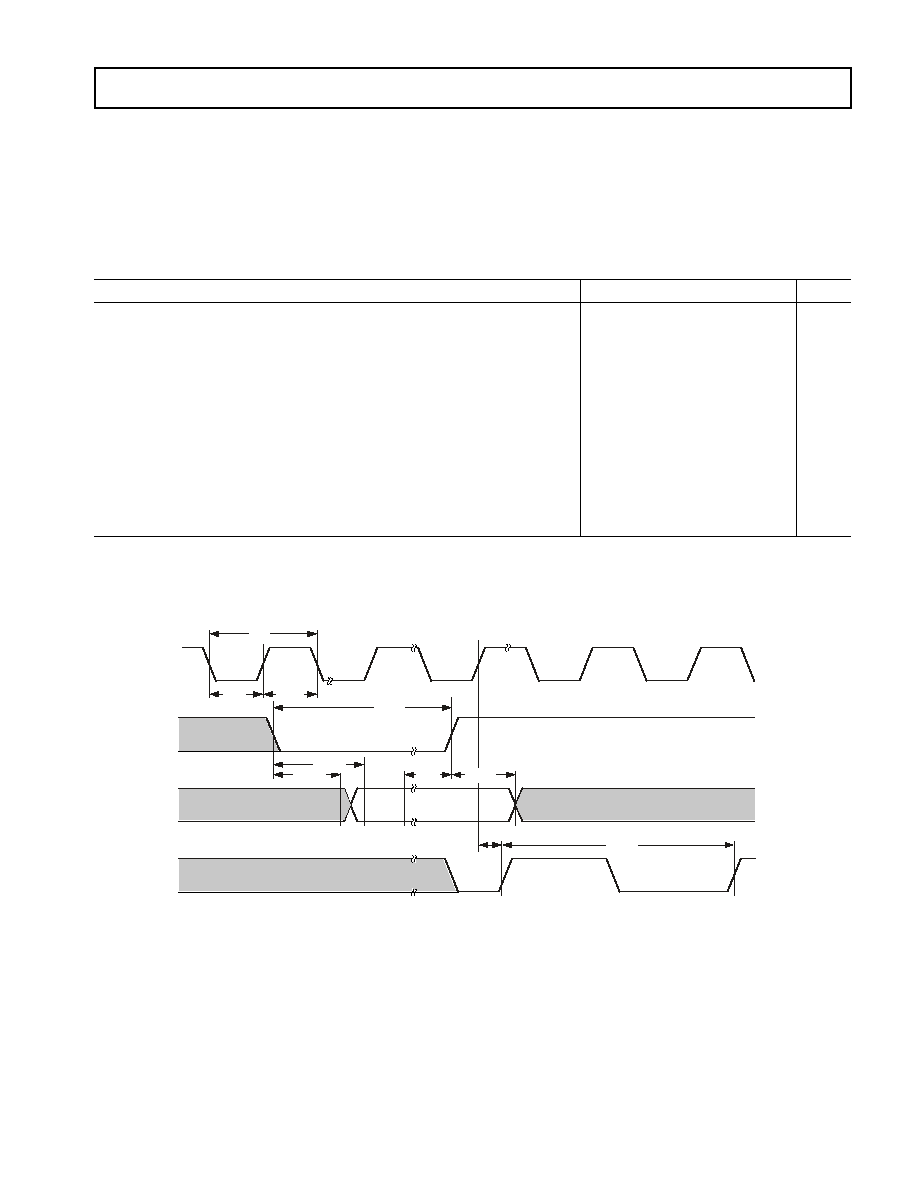
23
REV. 0
ADSP-21990
Clock In and Clock Out Cycle Timing
Table 5
and
Figure 6
describe clock and reset operations. Com-
binations of CLKIN and clock multipliers must not select
core/peripheral clocks in excess of 160 MHz/80 MHz for the
ADSP-21990BST and 150 MHz/75 MHz for the ADSP-
21990BBC, when the peripheral clock rate is one-half the core
clock rate. If the peripheral clock rate is equal to the core clock
rate, the maximum peripheral clock rate is 80 MHz for the
ADSP-21990BST and 75 MHz for the ADSP-21990BBC. The
peripheral clock is supplied to the CLKOUT pins.
When changing from bypass mode to PLL mode, allow 512
HCLK cycles for the PLL to stabilize.
Table 5. Clock In and Clock Out Cycle Timing
Parameter
Min
Max
Unit
Timing Requirements
t
CK
CLKIN Period
1,
2
10
200
ns
t
CKL
CLKIN Low Pulse
4.5
ns
t
CKH
CLKIN High Pulse
4.5
ns
t
WRST
RESET Asserted Pulsewidth Low
200t
CLKOUT
ns
t
MSS
MSELx/BYPASS Stable Before
RESET Deasserted Setup 40
µs
t
MSH
MSELx/BYPASS Stable After
RESET Deasserted Hold
1000
ns
t
MSD
MSELx/BYPASS Stable After
RESET Asserted
200
ns
t
PFD
Flag Output Disable Time After
RESET Asserted
10
ns
Switching Characteristics
t
CKOD
CLKOUT Delay from CLKIN
0
5.8
ns
t
CKO
CLKOUT Period
3
12.5
ns
1
In clock multiplier mode and MSEL60 set for 1:1 (or CLKIN = CCLK), t
CK
= t
CCLK
.
2
In bypass mode, t
CK
= t
CCLK
.
3
CLKOUT jitter can be as great as 8 ns when CLKOUT frequency is less than 20 MHz. For frequencies greater than 20 MHz, jitter is less than 1 ns.
Figure 6. Clock In and Clock Out Cycle Timing
t
CKOD
CLKOUT
MSEL60
BYPASS
DF
RESET
CLKIN
t
WRST
t
CKH
t
CK
t
CKL
t
MSH
t
CKO
t
PFD
t
MSD
t
MSS
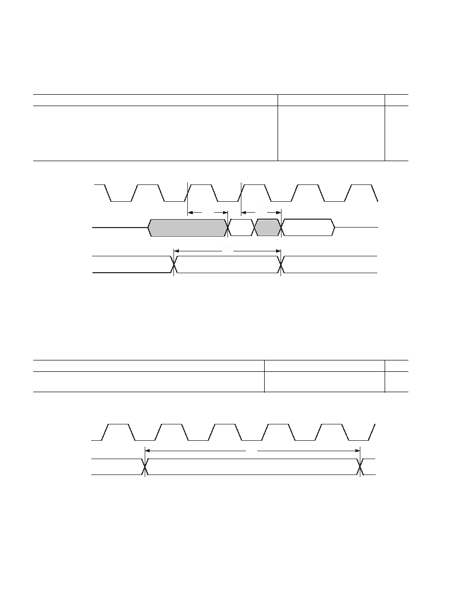
ADSP-21990
24
REV. 0
Programmable Flags Cycle Timing
Table 6
and
Figure 7
describe Programmable Flag operations.
Timer PWM_OUT Cycle Timing
Table 7
and
Figure 8
describe timer expired operations. The
input signal is asynchronous in "width capture mode" and has
an absolute maximum input frequency of 40 MHz.
Table 6. Programmable Flags Cycle Timing
Parameter
Min
Max
Unit
Timing Requirement
t
HFI
Flag Input Hold is Asynchronous
3
ns
Switching Characteristics
t
DFO
Flag Output Delay with Respect to CLKOUT
7
ns
t
HFO
Flag Output Hold After CLKOUT High
6
ns
Figure 7. Programmable Flags Cycle Timing
t
DFO
PF
(INPUT)
t
HFI
PF
(OUTPUT)
CLKOUT
FLAG INPUT
FLAG OUTPUT
t
HFO
Table 7. Timer PWM_OUT Cycle Timing
Parameter
Min
Max
Unit
Switching Characteristic
t
HTO
Timer Pulsewidth Output
1
12.5
(2
32
1) cycles
ns
1
The minimum time for t
HTO
is one cycle, and the maximum time for t
HTO
equals (2
32
1) cycles.
Figure 8. Timer PWM_OUT Cycle Timing
HCLK
PWM_OUT
t
HTO
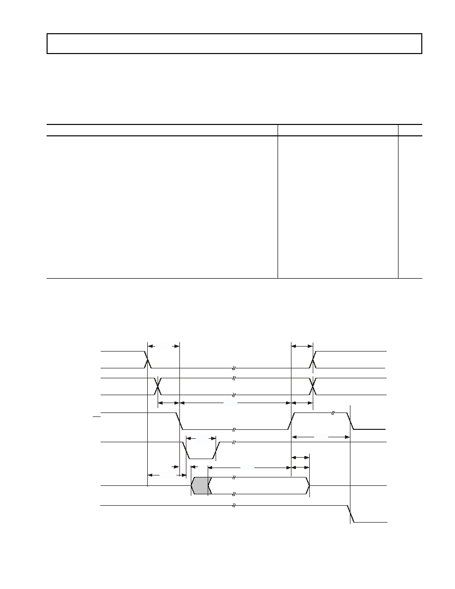
25
REV. 0
ADSP-21990
External Port Write Cycle Timing
Table 8
and
Figure 9
describe external port write operations.
The external port lets systems extend read/write accesses in three
ways: wait states, ACK input, and combined wait states and
ACK. To add waits with ACK, the DSP must see ACK low at
the rising edge of EMI clock. ACK low causes the DSP to wait,
and the DSP requires two EMI clock cycles after ACK goes high
to finish the access. For more information, see the External Port
chapter in the ADSP-2199x Mixed Signal DSP Controller
Hardware Reference.
Table 8. External Port Write Cycle Timing
Parameter
1, 2
Min
Max
Unit
Timing Requirements
t
AKW
ACK Strobe Pulsewidth
12.5
ns
t
DWSAK
ACK Delay from
XMS Low
0.5t
EMICLK
1
ns
Switching Characteristics
t
CSWS
Chip Select Asserted to
WR Asserted Delay
0.5t
EMICLK
4
ns
t
AWS
Address Valid to
WR Setup and Delay
0.5t
EMICLK
3
ns
t
WSCS
WR Deasserted to Chip Select Deasserted
0.5t
EMICLK
4
ns
t
WSA
WR Deasserted to Address Invalid
0.5t
EMICLK
3
ns
t
WW
WR Strobe Pulsewidth
t
EMICLK
2 + W
3
ns
t
CDA
WR to Data Enable Access Delay
0
ns
t
CDD
WR to Data Disable Access Delay
0.5t
EMICLK
3
0.5t
EMICLK
+ 4
ns
t
DSW
Data Valid to
WR Deasserted Setup
t
EMICLK
+ 1 +W
3
t
EMICLK
+ 7 + W
3
ns
t
DHW
WR Deasserted to Data Invalid Hold Time; E_WHC
4,
5
3.4
ns
t
DHW
WR Deasserted to Data Invalid Hold Time; E_WHC
4,
6
t
EMICLK
+ 3.4
ns
t
WWR
WR Deasserted to WR, RD Asserted
t
HCLK
ns
1
t
EMICLK
is the External Memory Interface clock period. t
HCLK
is the peripheral clock period.
2
These are timing parameters that are based on worst-case operating conditions.
3
W = (number of wait states specified in wait register) t
EMICLK
.
4
Write hold cyclememory select control registers (MS CTL).
5
Write wait state count (E_WWC) = 0
6
Write wait state count (E_WWC) = 1
Figure 9. External Port Write Cycle Timing
D150
t
AWS
t
WW
t
AKW
t
DHW
t
CDD
ACK
WR
A210
MS30
IOMS
BMS
t
CSWS
t
WSA
t
WSCS
t
CDA
RD
t
DSW
t
WWR
t
DWSAK
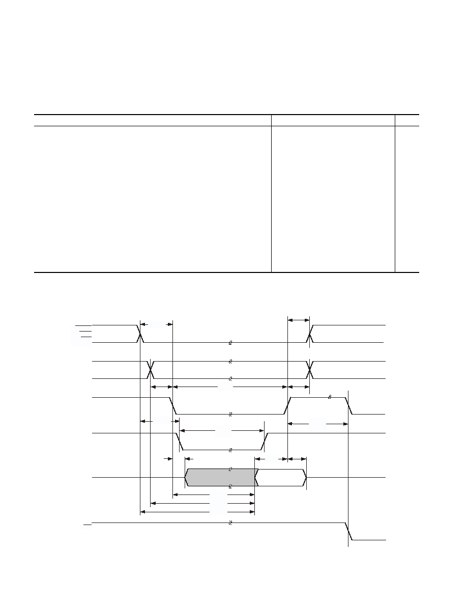
ADSP-21990
26
REV. 0
External Port Read Cycle Timing
Table 9
and
Figure 10
describe external port read operations.
For additional information on the ACK signal, see the discussion
on Page 25
.
Table 9. External Port Read Cycle Timing
Parameter
1, 2
Min
Max
Unit
Timing Requirements
t
AKW
ACK Strobe Pulsewidth
t
HCLK
ns
t
RDA
RD Asserted to Data Access Setup
t
EMICLK
5 +W
3
ns
t
ADA
Address Valid to Data Access Setup
t
EMICLK
+ W
3
ns
t
SDA
Chip Select Asserted to Data Access Setup
t
EMICLK
+ W
3
ns
t
SD
Data Valid to
RD Deasserted Setup
5
ns
t
HRD
RD Deasserted to Data Invalid Hold
0
ns
t
DRSAK
ACK Delay from
XMS Low
0.5t
EMICLK
1
ns
Switching Characteristics
t
CSRS
Chip Select Asserted to
RD Asserted Delay
0.5t
EMICLK
3
ns
t
ARS
Address Valid to
RD Setup and Delay
0.5t
EMICLK
3
ns
t
RSCS
RD Deasserted to Chip Select Deasserted Setup
0.5t
EMICLK
2
ns
t
RW
RD Strobe Pulsewidth
t
EMICLK
2 + W
3
ns
t
RSA
RD Deasserted to Address Invalid Setup
0.5t
HCLK
2
ns
t
RWR
RD Deasserted to WR, RD Asserted
t
HCLK
1
t
EMICLK
is the External Memory Interface clock period. t
HCLK
is the peripheral clock period.
2
These are timing parameters that are based on worst-case operating conditions.
3
W = (number of wait states specified in wait register) t
EMICLK
.
Figure 10. External Port Read Cycle Timing
t
ARS
D150
t
RW
t
AKW
t
CDA
t
RDA
t
ADA
t
SDA
t
S D
t
H R D
ACK
RD
A210
t
CSRS
t
RSA
t
RSCS
t
RWR
MS30
IOMS
BMS
WR
t
DRSAK
27
REV. 0
ADSP-21990
External Port Bus Request/Grant Cycle Timing
Table 10
and
Figure 11
describe external port bus request and
bus grant operations.
Table 10. External Port Bus Request and Grant Cycle Timing
Parameter
1, 2
Min
Max
Unit
Timing Requirements
t
BS
BR Asserted to CLKOUT High Setup
4.6
ns
t
BH
CLKOUT High to
BR Deasserted Hold Time
0
ns
Switching Characteristics
t
SD
CLKOUT High to
xMS, Address, and RD/WR Disable
0.5t
HCLK
+1
ns
t
SE
CLKOUT Low to
xMS, Address, and RD/WR Enable
0
4
ns
t
DBG
CLKOUT High to
BG Asserted Setup
0
4
ns
t
EBG
CLKOUT High to
BG Deasserted Hold Time
0
4
ns
t
DBH
CLKOUT High to
BGH Asserted Setup
0
4
ns
t
EBH
CLKOUT High to
BGH Deasserted Hold Time
0
4
ns
1
t
HCLK
is the peripheral clock period.
2
These are timing parameters that are based on worst-case operating conditions.
Figure 11. External Port Bus Request and Grant Cycle Timing
t
BH
A210
CLKOUT
t
BS
t
SD
t
SD
t
SD
t
DBG
t
DBH
t
SE
t
SE
t
SE
t
EBG
t
EBH
BGH
WR
RD
MS30
IOMS
BMS
BR
BG

ADSP-21990
28
REV. 0
Serial Port Timing
Table 11
and
Figure 12
describe SPORT transmit and receive
operations, while
Figure 13
and
Figure 14
describe SPORT
Frame Sync operations.
Table 11. Serial Port
1, 2
Parameter
Min
Max
Unit
External Clock Timing Requirements
t
SFSE
TFS/RFS Setup Before TCLK/RCLK
3
4
ns
t
HFSE
TFS/RFS Hold After TCLK/RCLK
3
4
ns
t
SDRE
Receive Data Setup Before RCLK
3
1.5
ns
t
HDRE
Receive Data Hold After RCLK
3
4
ns
t
SCLKW
TCLK/RCLK Width
0.5t
HCLK
1
ns
t
SCLK
TCLK/RCLK Period
2t
HCLK
ns
Internal Clock Timing Requirements
t
SFSI
TFS Setup Before TCLK
4
; RFS Setup Before RCLK
3
4
ns
t
HFSI
TFS/RFS Hold After TCLK/RCLK
3
3
ns
t
SDRI
Receive Data Setup Before RCLK
3
2
ns
t
HDRI
Receive Data Hold After RCLK
3
5
ns
External or Internal Clock Switching Characteristics
t
DFSE
TFS/RFS Delay After TCLK/RCLK (Internally
Generated FS)
4
14
ns
t
HOFSE
TFS/RFS Hold After TCLK/RCLK (Internally
Generated FS)
4
3
ns
External Clock Switching Characteristics
t
DDTE
Transmit Data Delay After TCLK
4
13.4
ns
t
HDTE
Transmit Data Hold After TCLK
4
4
ns
Internal Clock Switching Characteristics
t
DDTI
Transmit Data Delay After TCLK
4
13.4
ns
t
HDTI
Transmit Data Hold After TCLK
4
4
ns
t
SCLKIW
TCLK/RCLK Width
0.5t
HCLK
3.5
0.5t
HCLK
+ 2.5
ns
Enable and Three-State
5
Switching Characteristics
t
DTENE
Data Enable from External TCLK
4
0
12.1
ns
t
DDTTE
Data Disable from External TCLK
4
13
ns
t
DTENI
Data Enable from Internal TCLK
4
0
13
ns
t
DDTTI
Data Disable from External TCLK
4
12
ns
External Late Frame Sync Switching Characteristics
t
DDTLFSE
Data Delay from Late External TFS with MCE = 1, MFD = 0
6, 7
10.5
ns
t
DTENLFSE
Data Enable from Late FS or MCE = 1, MFD = 0
6, 7
3.5
ns
1
To determine whether communication is possible between two devices at clock speed n, the following specifications must be confirmed: 1) frame sync delay
and frame sync setup-and-hold, 2) data delay and data setup-and-hold, and 3) SCLK width.
2
Word selected timing for I
2
S mode is the same as TFS/RFS timing (normal framing only).
3
Referenced to sample edge.
4
Referenced to drive edge.
5
Only applies to SPORT.
6
MCE = 1, TFS enable, and TFS valid follow t
DDTENFS
and t
DDTLFSE
.
7
If external RFSD/TFS setup to RCLK/TCLK > 0.5t
LSCK
, t
DDTLSCK
and t
DTENLSCK
apply; otherwise, t
DDTLFSE
and t
DTENLFS
apply.
29
REV. 0
ADSP-21990
Figure 12. Serial Port
DT
DT
t
DDTTE
t
DDTEN
t
DDTTI
t
DDTIN
DRIVE
EDGE
DRIVE
EDGE
DRIVE
EDGE
DRIVE
EDGE
TCLK/RCLK
TCLK/RCLK
TCLK (EXT)
TFS ("LATE," EXT.)
t
SDRI
RCLK
RFS
DR
DRIVE
EDGE
SAMPLE
EDGE
t
HDRI
t
SFSI
t
HFSI
t
DFSE
t
HOFSE
t
SCLKIW
DATA RECEIVE-INTERNAL CLOCK
t
SDRE
DATA RECEIVE-EXTERNAL CLOCK
RCLK
RFS
DR
DRIVE
EDGE
SAMPLE
EDGE
t
HDRE
t
SFSE
t
HFSE
t
DFSE
t
SCLKW
t
HOFSE
NOTE: EITHER THE RISING EDGE OR FALLING EDGE OF RCLK OR TCLK CAN BE USED AS THE ACTIVE SAMPLING EDGE.
t
DDTI
t
HDTI
TCLK
TFS
DT
DRIVE
EDGE
SAMPLE
EDGE
t
SFSI
t
HFSI
t
SCLKIW
t
DFSE
t
HOFSE
DATA TRANSMIT-INTERNAL CLOCK
t
DDTE
t
HDTE
TCLK
TFS
DT
DRIVE
EDGE
SAMPLE
EDGE
t
SFSE
t
HFSE
t
DFSE
t
SCLKW
t
HOFSE
DATA TRANSMIT-EXTERNAL CLOCK
NOTE: EITHER THE RISING EDGE OR FALLING EDGE OF RCLK OR TCLK CAN BE USED AS THE ACTIVE SAMPLING EDGE.
TCLK (INT)
TFS ("LATE," INT.)
ADSP-21990
30
REV. 0
Figure 13. Serial Port--External Late Frame Sync (Frame Sync Setup > 0.5t
SCLK
)
Figure 14. Serial Port--External Late Frame Sync (Frame Sync Setup < 0.5t
HCLK
)
DRIVE
SAMPLE
DRIVE
t
DTENLFSE
t
DDTLFSE
EXTERNAL RFS WITH MCE = 1, MFD = 0
1ST BIT
2ND BIT
DT
RCLK
RFS
LATE EXTERNAL TFS
t
HDTE/ I
t
DDTE/ I
t
SFSE / I
DRIVE
SAMPLE
DRIVE
t
DTENLFSE
t
DDTLFSE
1ST BIT
2ND BIT
DT
TCLK
TFS
t
HDTE/ I
t
DDTE / I
t
HOSFSE/ I
t
HOSFSE/ I
t
SFSE/ I
t
DDTLFSE
DRIVE
SAMPLE
DRIVE
t
DTENLFSE
t
DDTLFSE
EXTERNAL RFS WITH MCE = 1, MFD = 0
1ST BIT
2ND BIT
DT
RCLK
RFS
LATE EXTERNAL TFS
t
HDTE/ I
t
DDTE / I
t
SFSE/ I
DRIVE
SAMPLE
DRIVE
t
DTENLFSE
1ST BIT
2ND BIT
DT
TCLK
TFS
t
HDTE/ I
t
DDTE/ I
t
HOFSE/ I
t
HOFSE/ I
t
SFSE/ I
31
REV. 0
ADSP-21990
Serial Peripheral Interface Port--Master Timing
Table 12
and
Figure 15
describe SPI port master operations.
Table 12. Serial Peripheral Interface (SPI) Port--Master Timing
Parameter
Min
Max
Unit
Timing Requirements
t
SSPID
Data Input Valid to SCLK Edge (Data Input Setup)
8
ns
t
HSPID
SCLK Sampling Edge to Data Input Invalid (Data In Hold)
1
ns
Switching Characteristics
t
SDSCIM
SPISEL Low to First SCLK Edge
2t
HCLK
3
ns
t
SPICHM
Serial Clock High Period
2t
HCLK
3
ns
t
SPICLM
Serial Clock Low Period
2t
HCLK
3
ns
t
SPICLK
Serial Clock Period
4t
HCLK
1
ns
t
HDSM
Last SCLK Edge to
SPISEL High
2t
HCLK
3
ns
t
SPITDM
Sequential Transfer Delay
2t
HCLK
2
ns
t
DDSPID
SCLK Edge to Data Output Valid (Data Out Delay)
0
6
ns
t
HDSPID
SCLK Edge to Data Output Invalid (Data Out Hold)
0
5
ns
Figure 15. Serial Peripheral Interface (SPI) Port--Master Timing
t
HSPID
t
HDSPID
LSB
MSB
t
HSPID
t
DDSPID
MOSI
(OUTPUT)
MISO
(INPUT)
SPISEL
(OUTPUT)
SCLK
(CPOL = 0)
(OUTPUT)
SCLK
(CPOL = 1)
(OUTPUT)
t
SPICHM
t
SPICLM
t
SPICLM
t
SPICLK
t
SPICHM
t
HDSM
t
SPITDM
t
HDSPID
LSB
VALID
LSB
MSB
MSB
VALID
t
HSPID
t
DDSPID
MOSI
(OUTPUT)
MISO
(INPUT)
t
SSPID
t
SDSCIM
t
SSPID
CPHA = 1
CPHA = 0
MSB
VALID
LSB
VALID
t
SSPID
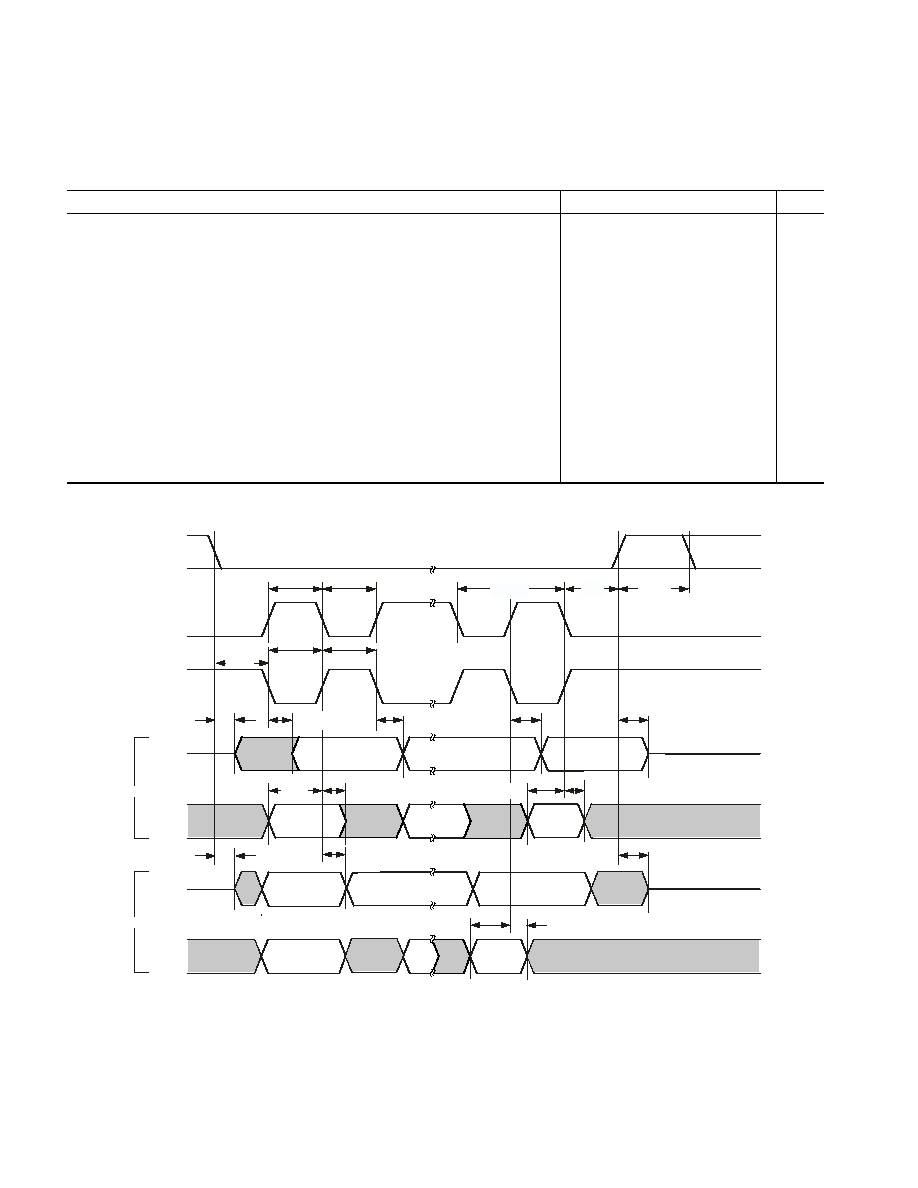
ADSP-21990
32
REV. 0
Serial Peripheral Interface Port--Slave Timing
Table 13
and
Figure 16
describe SPI port slave operations.
Table 13. Serial Peripheral Interface (SPI) Port--Slave Timing
Parameter
Min
Max
Unit
Timing Requirements
t
SPICHS
Serial Clock High Period
2t
HCLK
ns
t
SPICLS
Serial Clock Low Period
2t
HCLK
ns
t
SPICLK
Serial Clock Period
4t
HCLK
ns
t
HDS
Last SPICLK Edge to
SPISS Not Asserted
2t
HCLK
ns
t
SPITDS
Sequential Transfer Delay
2t
HCLK
+ 4
ns
t
SDSCI
SPISS Assertion to First SPICLK Edge
2t
HCLK
ns
t
SSPID
Data Input Valid to SCLK Edge (Data Input Setup)
1.6
ns
t
HSPID
SCLK Sampling Edge to Data Input Invalid (Data In Hold)
2.4
ns
Switching Characteristics
t
DSOE
SPISS Assertion to Data Out Active
0
8
ns
t
DSDHI
SPISS Deassertion to Data High Impedance
0
10
ns
t
DDSPID
SCLK Edge to Data Out Valid (Data Out Delay)
0
10
ns
t
HDSPID
SCLK Edge to Data Out Invalid (Data Out Hold)
0
10
ns
Figure 16. Serial Peripheral Interface (SPI) Port--Slave Timing
t
HSPID
t
DDSPID
t
DSDHI
LSB
MSB
MSB
VALID
t
HSPID
t
DSOE
t
HDSPID
MISO
(OUTPUT)
MOSI
(INPUT)
SPISS
(INPUT)
SCLK
(CPOL = 0)
(INPUT)
SCLK
(CPOL = 1)
(INPUT)
t
SPICHS
t
SPICLS
t
SPICLS
t
SPICLK
t
HDS
t
SPICHS
t
SSPID
t
HSPID
t
DSDHI
LSB
VALID
MSB
MSB
VALID
t
DSOE
t
DDSPID
MISO
(OUTPUT)
MOSI
(INPUT)
LSB
VALID
LSB
t
SPITDS
t
DDSPID
CPHA = 0
CPHA = 1
t
SDSCI
t
SSPID
t
SSPID
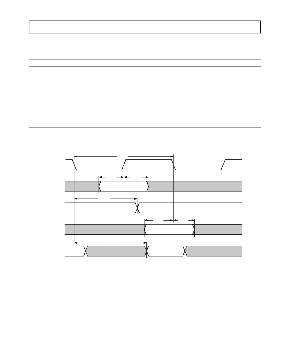
33
REV. 0
ADSP-21990
JTAG Test And Emulation Port Timing
Table 14
and
Figure 17
describe JTAG port operations.
Table 14. JTAG Port Timing
Parameter
Min
Max
Unit
Timing Requirements
t
TCK
TCK Period
20
ns
t
STAP
TDI, TMS Setup Before TCK High
4
ns
t
HTAP
TDI, TMS Hold After TCK High
4
ns
t
SSYS
System Inputs Setup Before TCK Low
1
4
ns
t
HSYS
System Inputs Hold After TCK Low
1
5
ns
t
TRSTW
TRST Pulsewidth
2
4t
TCK
ns
Switching Characteristics
t
DTDO
TDO Delay from TCK Low
8
ns
t
DSYS
System Outputs Delay After TCK Low
3
0
22
ns
1
System Inputs = DATA150, ADDR210, RD, WR, ACK, BR, BG, PF150, DR, TCLK, RCLK, TFS, RFS, CLKIN, RESET.
2
50 MHz maximum.
3
System Outputs = DATA150, ADDR210, MS30, RD,
WR, ACK, CLKOUT, BG, PF150, DT, TCLK0, TCLK, RCLK, TFS, RFS, BMS.
Figure 17. JTAG Port Timing
TMS
TDI
TDO
SYSTEM
INPUTS
SYSTEM
OUTPUTS
TCK
t
TCK
t
HTAP
t
STAP
t
DTDO
t
SSYS
t
HSYS
t
DSYS
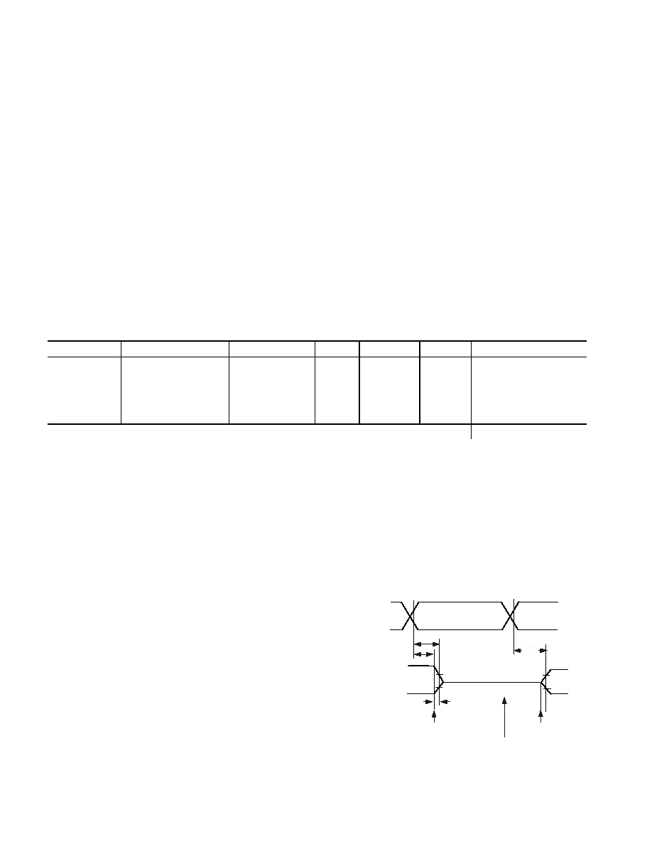
ADSP-21990
34
REV. 0
Power Dissipation
Total power dissipation has two components, one due to internal
circuitry and one due to the switching of external output drivers.
Internal power dissipation is dependent on the instruction
execution sequence and the data operands involved.
The external component of total power dissipation is caused by
the switching of output pins. Its magnitude depends on:
· Number of output pins that switch during each cycle (O)
· The maximum frequency at which they can switch (f)
· Their load capacitance (C)
· Their voltage swing (V
DD
)
and is calculated by the formula below.
The load capacitance includes the processor package capacitance
(C
IN
). The switching frequency includes driving the load high
and then back low. Address and data pins can drive high and low
at a maximum rate of 1/(2t
CK
). The write strobe can switch every
cycle at a frequency of 1/t
CK
. Select pins switch at 1/(2t
CK
), but
selects can switch on each cycle. For example, estimate P
EXT
with
the following assumptions:
· A system with one bank of external data memory--asyn-
chronous RAM (16-bit)
· One 64K 16 RAM chip is used with a load of 10 pF
· Maximum peripheral speed CCLK = 80 MHz, HCLK =
80 MHz
· External data memory writes occur every other cycle, a
rate of 1/(4t
HCLK
), with 50% of the pins switching
· The bus cycle time is 80 MHz (t
HCLK
= 12.5 ns)
The P
EXT
equation is calculated for each class of pins that can
drive as shown in
Table 15
.
A typical power consumption can now be calculated for these
conditions by adding a typical internal power dissipation with the
following formula.
Where:
· P
EXT
is from
Table 15
.
· P
INT
is I
DDINT
2.5 V, using the calculation I
DDINT
listed
in
Power Dissipation
.
Note that the conditions causing a worst-case P
EXT
are different
from those causing a worst-case P
INT
. Maximum P
INT
cannot
occur while 100% of the output pins are switching from all ones
to all zeros. Note also that it is not common for an application to
have 100% or even 50% of the outputs switching simultaneously.
Test Conditions
The DSP is tested for output enable, disable, and hold time.
Output Disable Time
Output pins are considered to be disabled when they stop driving,
go into a high impedance state, and start to decay from their
output high or low voltage. The time for the voltage on the bus
to decay by
V is dependent on the capacitive load, C
L
and the
load current, I
L
. This decay time can be approximated by the
following equation.
The output disable time t
DIS
is the difference between t
MEASURED
and t
DECAY
as shown in
Figure 18
. The time t
MEASURED
is the
interval from when the reference signal switches to when the
output voltage decays
V from the measured output high or
output low voltage. The t
DECAY
is calculated with test loads C
L
and
I
L
, and with
V equal to 0.5 V.
P
EXT
O
C
×
V
DD
2
×
f
×
=
Table 15. P
EXT
Calculation Example
Pin Type
Number of Pins
% Switching
C
f
V
DD
2
= P
EXT
Address
15
50
10 pF
20 MHz
10.9 V
= 0.01635 W
MSx
1
0
10 pF
20 MHz
10.9 V
= 0.0 W
WR
1
10 pF
40 MHz
10.9 V
= 0.00436 W
Data
16
50
10 pF
20 MHz
10.9 V
= 0.01744 W
CLKOUT
1
10 pF
80 MHz
10.9 V
= 0.00872 W
= 0.04687 W
P
TOTAL
P
=
EXT
P
INT
+
Figure 18. Output Enable/Disable
t
DECAY
C
L
V
I
L
---------------
=
REFERENCE
SIGNAL
t
DIS
OUTPUT STARTS
DRIVING
V
OH (MEASURED)
V 2.0V
V
OL (MEASURED)
+
V 1.0V
t
MEASURED
V
OH (MEASURED)
V
OL (MEASURED)
HIGH IMPEDANCE STATE.
TEST CONDITIONS CAUSE THIS VOLTAGE
TO BE APPROXIMATELY 1.5V
OUTPUT STOPS
DRIVING
t
DECAY
t
ENA
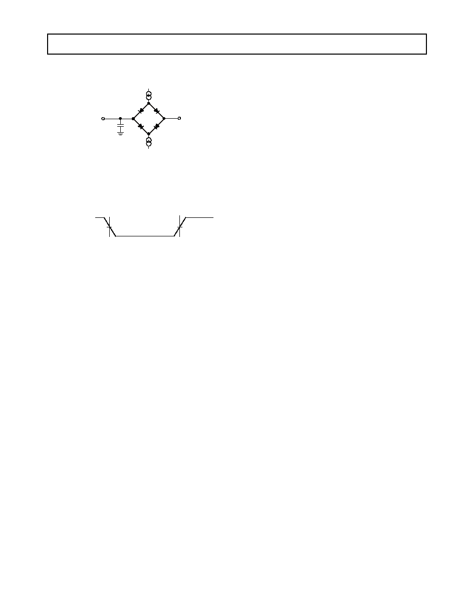
35
REV. 0
ADSP-21990
Output Enable Time
Output pins are considered to be enabled when they have made
a transition from a high impedance state to when they start
driving. The output enable time t
ENA
is the interval from when a
reference signal reaches a high or low voltage level to when the
output has reached a specified high or low trip point, as shown
in the Output Enable/Disable diagram (
Figure 18
). If multiple
pins (such as the data bus) are enabled, the measurement value
is that of the first pin to start driving.
Example System Hold Time Calculation
To determine the data output hold time in a particular system,
first calculate t
DECAY
using the equation at
Output Disable Time
on Page 34
. Choose
V to be the difference between the ADSP-
21990 output voltage and the input threshold for the device
requiring the hold time. A typical
V will be 0.4 V. C
L
is the total
bus capacitance (per data line), and I
L
is the total leakage or three-
state current (per data line). The hold time will be t
DECAY
plus the
minimum disable time (i.e., t
DATRWH
for the write cycle).
Pin Configurations
Table 16
identifies the signal for each Mini-BGA ball number.
Table 17
identifies the Mini-BGA ball number for each signal
name.
Table 18
identifies the signal for each LQFP lead.
Table 19
identifies the LQFP lead for each signal name.
Table 4
describes each pin name.
Figure 19. Equivalent Device Loading for AC
Measurements (Includes All Fixtures)
Figure 20. Voltage Reference Levels for AC
Measurements (Except Output Enable/Disable)
1.5V
50pF
TO
OUTPUT
PIN
I
OL
I
OH
INPUT
OR
OUTPUT
1.5V
1.5V

ADSP-21990
36
REV. 0
Table 16. 196-Ball Mini-BGA Ball Number by Signal
Pin Name
Ball No.
Pin Name
Ball No.
Pin Name
Ball No.
Pin Name
Ball No.
A0
N1
CONVST
G13
nc
E6
PF15
D14
A1
N2
D0
P10
nc
E7
POR H13
A2
M1
D1
N9
nc
E8
PWMPOL
M11
A3
M2
D2
P9
nc
E9
PWMSYNC
N13
A4
L1
D3
N8
nc
E10
PWMSR N14
A5
L2
D4
P8
nc
F5
PWMTRIP M12
A6
K1
D5
N7
nc
F6
RCLK
B2
A7
K2
D6
P7
nc
F7
RD C2
A8
J1
D7
N6
nc
F8
RESET H14
A9
J2
D8
P6
nc
F9
RFS
A4
A10
H1
D9
N5
nc
F10
SCK
B1
A11
H2
D10
P5
nc
G5
SENSE
B8
A12
G1
D11
N4
nc
G6
TCK
J13
A13
G2
D12
P4
nc
G7
TCLK
B3
A14
F1
D13
N3
nc
G8
TDI
J14
A15
F2
D14
P3
nc
G9
TDO
K14
A16
E1
D15
P2
nc
G10
TFS
B4
A17
E2
DR
A2
nc
H5
TMR0
H12
A18
D1
DT
A3
nc
H6
TMR1
G12
A19
D2
EIA
E12
nc
H7
TMR2
F13
ACK
D4
EIB
E13
nc
H8
TMS
J12
AH
N11
EIS
E14
nc
H9
TRST K13
AL
M10
EIZ
F12
nc
H10
VDDEXT
D11
ASHAN
B6
EMU K12
nc
J5
VDDEXT
E5
AUXTRIP
D10
GND
E4
nc
J6
VDDEXT
H11
AUX1
D12
GND
E11
nc
J7
VDDEXT
J4
AUX0
D13
GND
F4
nc
J8
VDDEXT
L4
AVDD
D5
GND
G11
nc
J9
VDDEXT
L6
AVDD
D6
GND
H4
nc
J10
VDDEXT
L9
AVSS
D7
GND
J11
nc
M8
VDDEXT
L10
AVSS
D8
GND
K4
nc
N12
VDDEXT
M5
BG F3
GND
K5
nc
P1
VDDEXT
M7
BGH G3
GND
K6
nc
P13
VDDINT
G4
BL
P11
GND
K7
nc
P14
VDDINT
L5
BH
P12
GND
K8
PF0/
SPISS
A10
VDDINT
L7
BMODE0
M14
GND
K9
PF1/SPISEL1
B10
VDDINT
L8
BMODE1
L13
GND
K10
PF2/SPISEL2
C10
VDDINT
K11
BMODE2
L12
GND
L11
PF3/SPISEL3
D9
VDDINT
F11
BMS J3
GND
M4
PF4/SPISEL4
A11
VIN0
A7
BR C1
GND
M6
PF5/SPISEL5
B11
VIN1
A8
BSHAN
A6
IOMS D3
PF6/SPISEL6
A12
VIN2
B7
BYPASS
M13
MISO
C3
PF7/SPISEL7
A13
VIN3
A9
CAPB
B9
MOSI
C4
PF8
B12
VIN4
A5
CAPT
C7
MS0 K3
PF9
B13
VIN5
C6
CH
N10
MS1 L3
PF10
C11
VIN6
B5
CL
M9
MS2 M3
PF11
C12
VIN7
C5
CLKIN
L14
MS3 H3
PF12
C13
VREF
C8
CLKOUT
G14
nc
A1
PF13
B14
WR E3
CML
C9
nc
A14
PF14
C14
XTAL
F14

37
REV. 0
ADSP-21990
Table 17. 196-Ball Mini-BGA Signal by Ball Number
Ball No.
Pin Name
Ball No.
Pin Name
Ball No.
Pin Name
Ball No.
Pin Name
A1
nc
D8
AVSS
H1
A10
L8
VDDINT
A2
DR
D9
PF3/SPISEL3
H2
A11
L9
VDDEXT
A3
DT
D10
AUXTRIP H3
MS3 L10
VDDEXT
A4
RFS
D11
VDDEXT
H4
GND
L11
GND
A5
VIN4
D12
AUX1
H5
nc
L12
BMODE2
A6
BSHAN
D13
AUX0
H6
nc
L13
BMODE1
A7
VIN0
D14
PF15
H7
nc
L14
CLKIN
A8
VIN1
E1
A16
H8
nc
M1
A2
A9
VIN3
E2
A17
H9
nc
M2
A3
A10
PF0/
SPISS
E3
WR H10
nc
M3
MS2
A11
PF4/SPISEL4
E4
GND
H11
VDDEXT
M4
GND
A12
PF6/SPISEL6
E5
VDDEXT
H12
TMR0
M5
VDDEXT
A13
PF7/SPISEL7
E6
nc
H13
POR M6
GND
A14
nc
E7
nc
H14
RESET M7
VDDEXT
B1
SCK
E8
nc
J1
A8
M8
nc
B2
RCLK
E9
nc
J2
A9
M9
CL
B3
TCLK
E10
nc
J3
BMS M10
AL
B4
TFS
E11
GND
J4
VDDEXT
M11
PWMPOL
B5
VIN6
E12
EIA
J5
nc
M12
PWMTRIP
B6
ASHAN
E13
EIB
J6
nc
M13
BYPASS
B7
VIN2
E14
EIS
J7
nc
M14
BMODE0
B8
SENSE
F1
A14
J8
nc
N1
A0
B9
CAPB
F2
A15
J9
nc
N2
A1
B10
PF1/SPISEL1
F3
BG J10
nc
N3
D13
B11
PF5/SPISEL5
F4
GND
J11
GND
N4
D11
B12
PF8
F5
nc
J12
TMS
N5
D9
B13
PF9
F6
nc
J13
TCK
N6
D7
B14
PF13
F7
nc
J14
TDI
N7
D5
C1
BR F8
nc
K1
A6
N8
D3
C2
RD F9
nc
K2
A7
N9
D1
C3
MISO
F10
nc
K3
MS0 N10
CH
C4
MOSI
F11
VDDINT
K4
GND
N11
AH
C5
VIN7
F12
EIZ
K5
GND
N12
nc
C6
VIN5
F13
TMR2
K6
GND
N13
PWMSYNC
C7
CAPT
F14
XTAL
K7
GND
N14
PWMSR
C8
VREF
G1
A12
K8
GND
P1
nc
C9
CML
G2
A13
K9
GND
P2
D15
C10
PF2/SPISEL2
G3
BGH K10
GND
P3
D14
C11
PF10
G4
VDDINT
K11
VDDINT
P4
D12
C12
PF11
G5
nc
K12
EMU P5
D10
C13
PF12
G6
nc
K13
TRST P6
D8
C14
PF14
G7
nc
K14
TDO
P7
D6
D1
A18
G8
nc
L1
A4
P8
D4
D2
A19
G9
nc
L2
A5
P9
D2
D3
IOMS G10
nc
L3
MS1 P10
D0
D4
ACK
G11
GND
L4
VDDEXT
P11
BL
D5
AVDD
G12
TMR1
L5
VDDINT
P12
BH
D6
AVDD
G13
CONVST
L6
VDDEXT
P13
nc
D7
AVSS
G14
CLKOUT
L7
VDDINT
P14
nc

ADSP-21990
38
REV. 0
Table 18. 176-Lead LQFP Signal by Lead Number
Lead No.
Signal
Lead No.
Signal
Lead No.
Signal
Lead No.
Signal
1
nc
45
VDDEXT
89
nc
133
VDDEXT
2
nc
46
A4
90
nc
134
PF11
3
VDDEXT
47
A3
91
VDDEXT
135
PF10
4
RCLK
48
A2
92
BYPASS
136
PF9
5
SCK
49
A1
93
BMODE0
137
PF8
6
MISO
50
A0
94
BMODE1
138
PF7/SPISEL7
7
MOSI
51
D15
95
BMODE2
139
PF6/SPISEL6
8
RD
52
D14
96
nc
140
PF5/SPISEL5
9
WR
53
D13
97
GND
141
PF4/SPISEL4
10
ACK
54
D12
98
VDDINT
142
GND
11
BR
55
D11
99
EMU
143
VDDEXT
12
BG
56
GND
100
TRST
144
PF3/SPISEL3
13
BGH
57
VDDEXT
101
TDO
145
PF2/SPISEL2
14
IOMS
58
GND
102
TDI
146
PF1/SPISEL1
15
BMS
59
VDDINT
103
TMS
147
PF0/
SPISS
16
MS3
60
D10
104
TCK
148
GND
17
GND
61
D9
105
POR
149
VDDINT
18
VDDEXT
62
D8
106
RESET
150
AVSS
19
MS2
63
D7
107
CLKIN
151
AVDD
20
MS1
64
D6
108
XTAL
152
nc
21
MS0
65
D5
109
CLKOUT
153
VREF
22
GND
66
GND
110
CONVST
154
CML
23
VDDINT
67
VDDINT
111
TMR0
155
CAPT
24
A19
68
D4
112
GND
156
CAPB
25
A18
69
D3
113
VDDEXT
157
SENSE
26
A17
70
D2
114
TMR1
158
VIN3
27
A16
71
D1
115
TMR2
159
VIN2
28
A15
72
D0
116
EIS
160
VIN1
29
A14
73
nc
117
GND
161
VIN0
30
A13
74
GND
118
VDDINT
162
ASHAN
31
GND
75
VDDEXT
119
EIZ
163
BSHAN
32
VDDEXT
76
CL
120
EIB
164
VIN4
33
A12
77
CH
121 EIA
165
VIN5
34
A11
78
BL
122
AUXTRIP
166
VIN6
35
A10
79
BH
123
AUX1
167
VIN7
36
A9
80
AL
124
AUX0
168
AVSS
37
A8
81
AH
125
PF15
169
AVDD
38
A7
82
nc
126
PF14
170
DT
39
A6
83 nc
127
PF13
171
DR
40
A5
84
PWMSYNC
128
PF12
172
RFS
41
GND
85 PWMPOL
129
GND
173
TFS
42
nc
86
PWMSR
130
nc
174
TCLK
43
nc
87
PWMTRIP
131
nc
175
GND
44
nc
88
GND
132
nc
176
nc

39
REV. 0
ADSP-21990
Table 19. 176-Lead LQFP Lead Number by Signal
Signal
Lead No.
Signal
Lead No.
Signal
Lead No.
Signal
Lead No.
A0
50
CAPB
156
EIS
116
PWMTRIP
87
A1
49
CAPT
155
EIZ
119
RCLK
4
A10
35
CH
77
EMU
99
RD
8
A11
34
CL
76
IOMS
14
RESET
106
A12
33
CLKIN
107
MISO
6
RFS
172
A13
30
CLKOUT
109
MOSI
7
SCK
5
A14
29
CML
154
MS0
21
SENSE
157
A15
28
CONVST
110
MS1
20
TCK
104
A16
27
D0
72
MS2
19
TCLK
174
A17
26
D1
71
MS3
16
TDI
102
A18
25
D10
60
nc
1
TDO
101
A19
24
D11
55
nc
2
TFS
173
A2
48
D12
54
nc
42
TMR0
111
A3
47
D13
53
nc
43
TMR1
114
A4
46
D14
52
nc
44
TMR2
115
A5
40
D15
51
nc
83
TMS
103
A6
39
D2
70
nc
89
TRST
100
A7
38
D3
69
nc
90
VDDEXT
3
A8
37
D4
68
nc
96
VDDEXT
18
A9
36
D5
65
nc
130
VDDEXT
32
ACK
10
D6
64
nc
131
VDDEXT
45
AH
81
D7
63
nc
132
VDDEXT
57
AL
80
D8
62
nc
152
VDDEXT
75
ASHAN
162
D9
61
nc
176
VDDEXT
91
AUX0
124
GND
17
PF0/
SPISS
147
VDDEXT
113
AUX1
123
GND
22
PF1/SPISEL1
146
VDDEXT
133
AUXTRIP
122
GND
31
PF10
135
VDDEXT
143
AVDD
151
GND
41
PF11
134
VDDINT
23
AVDD
169
GND
56
PF12
128
VDDINT
59
AVSS
150
GND
58
PF13
127
VDDINT
67
AVSS
168
GND
66
PF14
126
VDDINT
98
BG
12
GND
74
PF15
125
VDDINT
118
BGH
13
GND
88
PF2/SPISEL2
145
VDDINT
149
BH
79
GND
97
PF3/SPISEL3
144
VIN0
161
BL
78
GND
112
PF4/SPISEL4
141
VIN1
160
BMODE0
93
GND
117
PF5/SPISEL5
140
VIN2
159
BMODE1
94
GND
129
PF6/SPISEL6
139
VIN3
158
BMODE2
95
GND
142
PF7/SPISEL7
138
VIN4
164
BMS
15
GND
148
PF8
137
VIN5
165
BR
11
GND
175
PF9
136
VIN6
166
BSHAN
163
DR
171
POR
105
VIN7
167
BYPASS
92
DT
170
PWMPOL
85 VREF
153
nc
73
EIA
121
PWMSR
86
WR
9
nc
82
EIB
120
PWMSYNC
84 XTAL
108
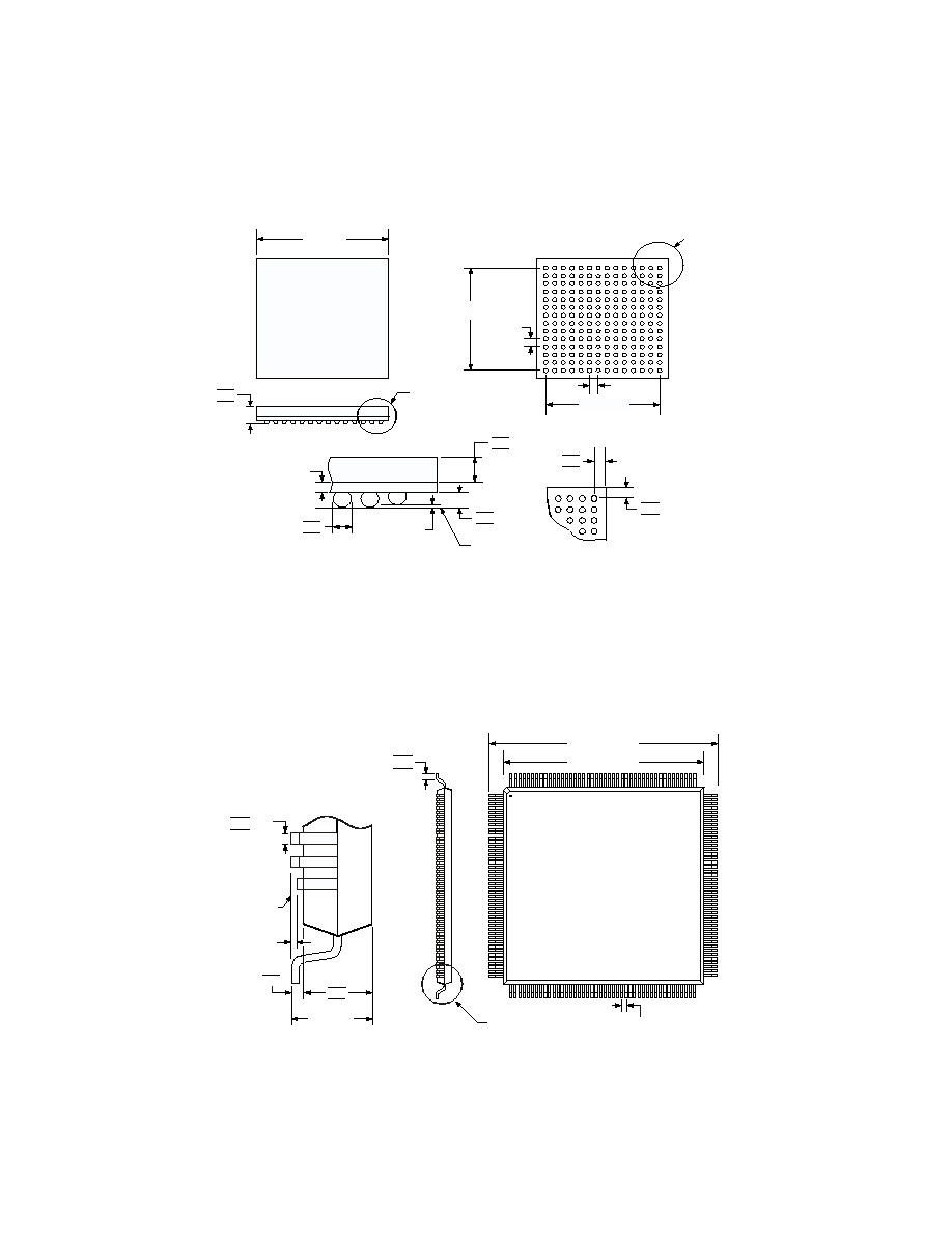
ADSP-21990
40
REV. 0
OUTLINE DIMENSIONS
Dimensions shown in millimeters.
196-Ball Mini-BGA (BC-196-2)
176-Lead LQFP (ST-176-1)
DETAIL B
DETAIL A
SEAT IN G PLANE
DET AIL A
BALL
DIAM ETER
0.55
NO M
0.20
MAX BALL
COPLANAR IT Y
13.00 BSC
A
B
C
D
E
F
G
H
J
K
L
M
N
P
9 8 7 6 5 4 3 2 1
DETAIL B
1.00 BSC
15.00
BSC SQ
TO P VIEW
BO TTO M VIEW
1.00 BSC
N OTES:
1. THE ACTUAL POSITION O F THE BALL G RID IS W ITHIN 0.25 OF IT S IDEAL POSITIO N REL ATIVE TO
THE PACKAGE ED GES.
2. THE ACTUAL POSITION O F EACH BAL L IS W ITHIN 0.10 OF IT S IDEAL POSITIO N RELAT IVE TO THE
BALL GRID.
3. DIMENSIONS COM PLY WITH JEDEC STANDARD M O-192 VARIATION AAE-1 W ITH THE EXCEPT ION
OF M AXIM UM H EIG HT.
4. CENTER DIM ENSIONS ARE NO MINAL.
1.85
1.70
1.55
13.00
BSC
10
11
12
13
14
0.70
0.60
0.50
0.57
0.52
0.47
0.75
0.70
0.65
1.10
1.00
0.90
1.10
1.00
0.90
TOP VIEW (PINS DOWN)
PIN 1
133
1
132
45
44
88
89
176
26.00
BSC SQ
24.00 BSC SQ
0.27
0.22 TYP
0.17
0.50 BSC
LEAD PITCH
0.75
0.60
0.45
SEATING
PLANE
1.60 MAX
0.15
0.05
0.08 MAX LEAD
COPLANARITY
1.45
1.40
1.35
DETAIL A
NOTES:
1.
DIMENSIONS IN MILLIMETERS.
2.
ACTUAL POSITION OF EACH LEAD IS WITHIN 0.08 OF ITS IDEAL POSITION,
WHEN MEASURED IN THE LATERAL DIRECTION.
3.
CENTER DIMENSIONS ARE NOMINAL.
4. DIMENSIONS COMPLY WITH JEDEC STANDARD MS-026-BGA.
DETAIL A

41
REV. 0
ADSP-21990
ORDERING GUIDE
Part Number
Ambient Temperature Range Instruction Rate
Operating Voltage
Package
ADSP-21990BBC
40ºC to +85ºC
150 MHz
2.5 Int./3.3 Ext. V
196-Ball Mini-BGA
ADSP-21990BST
40ºC to +85ºC
160 MHz
2.5 Int./3.3 Ext. V
176-Lead LQFP

42

43

44
C0
28
93
0
5/
03
(
0)
Document Outline