Äîêóìåíòàöèÿ è îïèñàíèÿ www.docs.chipfind.ru
a
Preliminary Technical Data
MultiPort Internet
Gateway Processor
This information applies to a product under development. Its characteristics
and specifications are subject to change without notice. Analog Devices
assumes no obligation regarding future manufacturing unless otherwise
agreed to in writing.
One Technology Way, P.O.Box 9106, Norwood, MA 02062-9106, U.S.A.
Tel:781/329-4700
World Wide Web Site: http://www.analog.com
Fax:781/326-8703
©Analog Devices,Inc., 2001
REV. PrB
6/2001
ADSP-21mod980N
PERFORMANCE FEATURES
Complete Single Device Multi-Port Internet Gateway
Processor (No External Memory Required)
Implements Sixteen Modem Channels or Forty Voice
Channels in One Package
Each DSP Can Implement two V.34/V.90 Data/Fax
Modem Channels (includes Datapump and
Controller)
Low Power Version: 640 MIPS Sustained Performance,
12.5 ns Instruction Time @ 1.9 Volts nominal
(internal)
Open Architecture Extensible to Voice-over-Network
(VoN) and Other Applications
Low Power Dissipation, 25 mW (typical) per Channel
Powerdown Mode Featuring Low CMOS Standby Power
Dissipation
INTEGRATION FEATURES
ADSP-2100 Family Code-Compatible, with Instruction
Set Extensions
16 Mbits of On-Chip SRAM, Configured as 9 Mbits of
Program Memory and 7 Mbits of Data Memory
Dual-Purpose Program Memory, for Both Instruction
and Data Storage
352-Ball PBGA with a 35mm 35mm footprint
SYSTEM CONFIGURATION FEATURES
16-Bit Internal DMA Port for High-Speed Access to
On-Chip Memory (Mode-Selectable)
Programmable Multichannel Serial Port Supports 24/32
Channels
Two Double-Buffered Serial Ports with Companding
Hardware and Automatic Data Buffering
Separate Reset Pins for Each Internal Processor
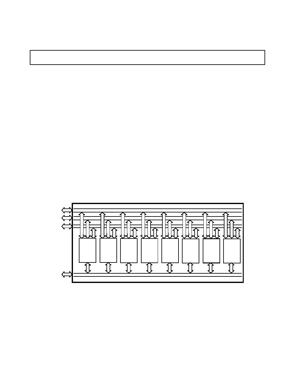
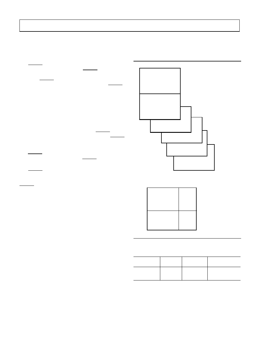
Figure 1. MOD980N MultiPort Internet Gateway Processor Block Diagram
2188N
DSP 1
2188N
DSP 2
2188N
DSP 3
2188N
DSP 4
2188N
DSP 5
2188N
DSP 6
2188N
DSP 8
2188N
DSP 7
Host IDMA
SPORT0
SPORT1
CONTROL
21m od980N

2
6/2001 REV. PrB
For current information contact Analog Devices at (800) ANALOGD
ADSP-21mod980N
PRELIMINARY TECHNICAL DATA
GENERAL DESCRIPTION
The ADSP-21mod980N is a multi-port Internet gateway
processor optimized for implementation of a complete
V.34/V.90 digital modem. All datapump and controller
functions can be implemented on a single device, offering
the lowest power consumption and highest possible modem
port density.
The ADSP-21mod980N combines the ADSP-2100 Family
base architecture (three computational units, data address
generators, and a program sequencer) with two serial ports,
a 16-bit internal DMA port, a byte DMA port, a program-
mable timer, Flag I/O, extensive interrupt capabilities, and
on-chip program and data memory.
The ADSP-21mod980N integrates 16 Mbits of on-chip
memory, configured as 384 Kwords (24-bit) of program
RAM, and 448 Kwords (16-bit) of data RAM. Power-down
circuitry is also provided to reduce the average and standby
power consumption of equipment which in turn reduces
equipment cooling requirements. The ADSP-21mod980N
is available in a 35 mm x 35 mm, 352-lead PBGA package.
Fabricated in a high-speed, low-power, CMOS process, the
ADSP-21mod980N operates with a 12.5 ns instruction
cycle time. Every instruction can execute in a single proces-
sor cycle.
The ADSP-21mod980N's flexible architecture and com-
prehensive instruction set allow the processor to perform
multiple operations in parallel. In one processor cycle, the
ADSP-21mod980N can:
·
Generate the next program address
·
Fetch the next instruction
·
Perform one or two data moves
·
Update one or two data address pointers
·
Perform a computational operation
This takes place while the processor continues to:
·
Receive and transmit data through the two serial ports
·
Receive and/or transmit data through the internal
DMA port
·
Receive and/or transmit data through the byte DMA
port
·
Decrement timer
MODEM SOFTWARE
The following software is available as object code from
Analog Devices Inc.
·
ADSP-21mod Family Dynamic Internet Voice
Access
TM
(DIVA) Voice Over Network Solution.
·
ADSP-21mod980-210N Multiport Internet Gateway
Processor Modem Solution.
A complete system implementation requires the
ADSP-21mod980N device plus modem or voice software.
The modem software executes general modem control,
command sets, error correction, and data compression,
data modulations (for example, V.34 and V.90), and host
interface functions.The host interface allows system access
to modem statistics, such as call progress, connect speed,
retrain count, symbol rate, and other modulation
parameters.
The modem datapump and controller software reside in
on-chip SRAM and do not require additional memory. You
can configure the ADSP-21mod980N dynamically by
downloading software from the host through the 16-bit
IDMA interface. This SRAM-based architecture provides a
software upgrade path to other applications, such as
voice-over-IP, and to future standards.
DEVELOPMENT SYSTEM
Analog Devices' wide range of software and hardware devel-
opment tools supports the ADSP-218x N Series. The DSP
tools include an integrated development environment
(IDE), an evaluation kit, and a serial port emulator.
VisualDSP® is an integrated development environment,
allowing for fast and easy development, debug and deploy-
ment. The VisualDSP project management environment
lets programmers develop and debug an application. This
environment includes an easy-to-use assembler that is based
on an algebraic syntax; an archiver (librarian/library
builder); a linker; a loader; a cycle-accurate, instruc-
tion-level simulator; a C compiler; and a C run-time library
that includes DSP and mathematical functions.
Debugging both C and assembly programs with the Visu-
alDSP debugger, programmers can:
· View mixed C and assembly code (interleaved source and
object information)
· Insert break points
· Set conditional breakpoints on registers, memory, and
stacks
· Trace instruction execution
· Fill and dump memory
· Source level debugging

3
REV. PrB
6/2001
For current information contact Analog Devices at (800) ANALOGD
ADSP-21mod980N
PRELIMINARY TECHNICAL DATA
The VisualDSP IDE lets programmers define and manage
DSP software development. The dialog boxes and property
pages let programmers configure and manage all of the
ADSP-218x development tools, including the syntax high-
lighting in the VisualDSP editor. This capability controls
how the development tools process inputs and generate
outputs.
The ADSP-218x EZ-ICE ® Emulator provides an easier
and more cost-effective method for engineers to develop
and optimize DSP systems, shortening product develop-
ment cycles for faster time-to-market. The
ADSP-21mod980N integrates on-chip emulation support
with a 14-pin ICE-Port interface. This interface provides a
simpler target board connection that requires fewer
mechanical clearance considerations than other
ADSP-2100 Family EZ-ICEs. The ADSP-21mod980N
device need not be removed from the target system when
using the EZ-ICE, nor are any adapters needed. Due to the
small footprint of the EZ-ICE connector, emulation can be
supported in final board designs.The EZ-ICE performs a
full range of functions, including:
· In-target operation
· Up to 20 breakpoints
· Single-step or full-speed operation
· Registers and memory values can be examined and
altered
· PC upload and download functions
· Instruction-level emulation of program booting and
execution
· Complete assembly and disassembly of instructions
· C source-level debugging
ADDITIONAL INFORMATION
This data sheet provides a general overview of
ADSP-21mod980N functionality. For specific information
about the modem processors, refer to the ADSP-2188N
data sheet. For additional information on the architecture
and instruction set of the modem processors, refer to the
ADSP-2100 Family User's Manual (3rd edition). For more
information about the development tools, refer to the
ADSP-2100 Family Development Tools Data Sheet.
4
6/2001 REV. PrB
For current information contact Analog Devices at (800) ANALOGD
ADSP-21mod980N
PRELIMINARY TECHNICAL DATA
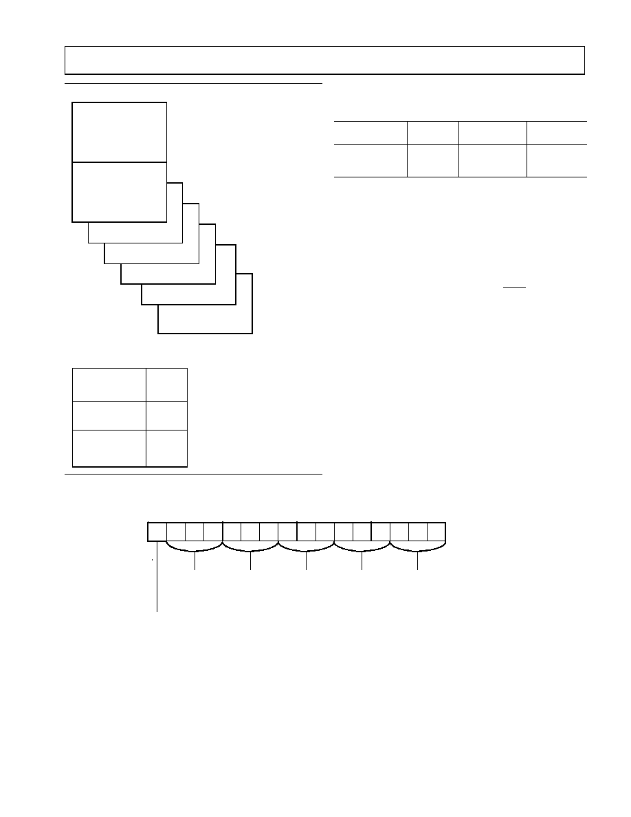
ARCHITECTURE OVERVIEW
Figure 2 on page 4 is a functional block diagram of the
ADSP-21mod980N. It contains eight independent digital
signal processors.
Every modem processor has:
·
A DSP core
·
256K bytes of RAM
·
Two serial ports
·
An IDMA host.
The signals of each modem processor are accessed through
the external pins of the ADSP-21mod980N. Some signals
are bussed with the signals of the other processors and are
accessed through a single external pin. Other signals remain
separate and they are accessed through separate external
pins for each processor.
The arrangement of the eight modem processors in the
ADSP-21mod980N makes one basic configuration possi-
ble: a slave configuration. In this configuration, the data
pins of all eight processors connect to a single bus structure.
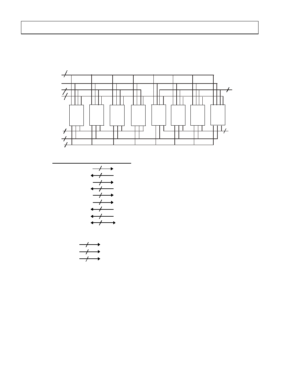
Figure 2. ADSP-21mod980N Functional Block Diagram
IAD<15:0>, IDM A CNTL
P F<0:2>/M OD E A:C
20
3
2188N
2188N
2188N
2188N
2188N
17
2188N
4
4
8
4
2188N
2188N
20
S P ORT1
S P ORT0A
CLKIN
E M ULATOR
S UBTO TAL = 177 S IG NAL BALLS
SIGNALS RO UTE D TO E ACH RE S P E CTIV E DIE
8
BG <8:1>
8
BR <8:1>
E E <8:1>
8
IS <8:1>
8
RE S E T <8:1>
8
CLKOUT <8:1>
8
TFS 0 <8:1>
8
DT1 <8:1>
8
INTE RRUP TS < 8:1>
32
22
V DDINT
44
V DDE XT
S UBTO TAL = 175 P OW E R BALLS
TOTAL = 352 BALLS
109
GND
DATA< 23:8>, A<0 >
IAD <15:0>,
IDM A CNTL
S P ORT0B
IDM A CNTL = IAL, IRD, IW R, IACK
INTE RRUP TS = IRQE (P F4), IRQL 0(P F5), IRQL1(P F6), IRQ2(P F7)
EM ULATOR = E M S , E INT, E LIN, E BR, E BG, E CLK
E LOUT, E RE S E T
S P ORT0A, S PO RT 0B
= RFS 0, DR0, DT0, S CKL0
S P ORT1 = RFS 1, TFS 1, DR1, S CKL1
NOTE :
1. P W D AND P F3/M ODE D ARE TIE D HIGH
DS P 1
DS P 2
DS P 3
DS P 4
DS P 5
DS P 6
DS P 7
DS P 8

5
REV. PrB
6/2001
For current information contact Analog Devices at (800) ANALOGD
ADSP-21mod980N
PRELIMINARY TECHNICAL DATA
All eight modem processors have identical functions and
have equal status. Each of the modem processors is con-
nected to a common IDMA bus and each modem processor
is configured to operate in the same mode (see the slave
mode and the memory mode descriptions in
"Memory
Architecture" on page 10
). The slave mode is considered to
be the only mode of operation in the ADSP-21mod980N
modem pool.
SERIAL PORTS
The ADSP-21mod980N has a multichannel serial port
(SPORT) connected to each internal digital modem pro-
cessor for serial communications.
The following is a brief list of ADSP-21mod980N SPORT
features. For additional information on the internal Serial
Ports, refer to the ADSP-2100 Family User's Manual. Each
SPORT:
·
is bidirectional and has a separate, double-buffered
transmit and receive section.
·
can use an external serial clock or generate its own
serial clock internally.
·
has independent framing for the receive and transmit
sections. Sections run in a frameless mode or with
frame synchronization signals internally or externally
generated. Frame sync signals are active high or
inverted, with either of two pulse widths and timings.
·
supports serial data word lengths from 3 to 16 bits and
provides optional A-law and µ-law companding accord-
ing to CCITT recommendation G.711.
·
receive and transmit sections can generate unique
interrupts on completing a data word transfer.
·
can receive and transmit an entire circular buffer of
data with one overhead cycle per data word. An inter-
rupt is generated after a data buffer transfer.
A multichannel interface selectively receives and transmits a
24 or 32 word, time-division multiplexed, serial bitstream.
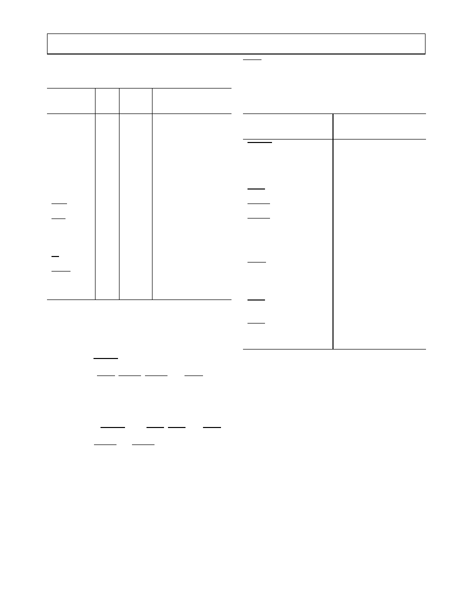
PIN DESCRIPTIONS
The ADSP-21mod980N is available in a 352-lead PBGA
package. In order to maintain maximum functionality and
reduce package size and pin count, some serial port, pro-
grammable flag, interrupt and external bus pins have dual,
multiplexed functionality. The external bus pins are config-
ured during RESET only, while serial port pins are software
configurable during program execution. Flag and interrupt
functionality is retained concurrently on multiplexed pins.
Table on page 6
lists the pin names and their functions. In
cases where pin functionality is reconfigurable, the default
state is shown in plain text; alternate functionality is shown
in italics.

6
6/2001 REV. PrB
For current information contact Analog Devices at (800) ANALOGD
ADSP-21mod980N
PRELIMINARY TECHNICAL DATA
MEMORY INTERFACE PINS
The ADSP-21mod980N modem pool is used in Slave
Mode. In Slave Mode, the Modem Processors operate in
host configuration. The operating mode is determined by
the state of the Mode C pin during RESET and cannot be
changed while the modem pool is running. See the "Mem-
ory Architecture" section for more information.
Table 1. Common Mode Pins
Pin Name(s)
# of Pins
Input/Output
Function
RESET
8
I
Processor Reset Input
BR
8
I
Bus Request Input
BG
8
O
Bus Grant Output
IRQ2 /
8
I
Edge- or Level-Sensitive Interrupt Request
1
PF7
8
I/O
Programmable I/O Pin
IRQL1 /
8
I
Level-Sensitive Interrupt Requests
1
PF6
8
I/O
Programmable I/O Pin
IRQL0 /
8
I
Level-Sensitive Interrupt Requests
1
PF5
8
I/O
Programmable I/O Pin
IRQE /
8
I
Edge-Sensitive Interrupt Requests
1
PF4
8
I/O
Programmable I/O Pin
Mode C /
1
I
Mode Select Input - Checked Only During RESET
PF2
1
I/O
Programmable I/O Pin During Normal Operation
Mode B /
1
I
Mode Select Input - Checked Only During RESET
PF1
1
I/O
Programmable I/O Pin During Normal Operation
Mode A /
1
I
Mode Select Input - Checked Only During RESET
PF0
1
I/O
Programmable I/O Pin During Normal Operation
CLKIN
1
I
Clock Input
CLKOUT
8
O
Processor Clock Output
SPORT
28
I/O
Serial Port I/O Pins
2
V
DD
and GND
175
I
Power and Ground
EZ-Port
16
I/O
For Emulation Use
1
Interrupt/Flag Pins retain both functions concurrently. If IMASK is set to enable the corresponding interrupts, then the ADSP-21mod980N will vector
to the appropriate interrupt vector address when the pin is asserted, either by external devices, or set as a programmable flag.
2
SPORT configuration determined by the ADSP-21mod980N System Control Register. Software configurable.
7
REV. PrB
6/2001
For current information contact Analog Devices at (800) ANALOGD
ADSP-21mod980N
PRELIMINARY TECHNICAL DATA
INTERRUPTS
The interrupt controller allows each modem processor in
the modem pool to respond individually to eleven possible
interrupts and RESET with minimum overhead. The
ADSP-21mod980N provides four dedicated external inter-
rupt input pins, IRQ2, IRQL1, IRQL0, and IRQE (shared
with the PF[7:4] pins) for each modem processor. The
ADSP-21mod980N also supports internal interrupts from
the timer, the byte DMA port, the serial port, software, and
the power-down control circuit. The interrupt levels are
internally prioritized and individually maskable (except
power down and RESET). The IRQ2, IRQ1, and IRQ0
input pins can be programmed to be either level- or
edge-sensitive. IRQL0 and IRQL1 are level-sensitive and
IRQE is edge sensitive. The priorities and vector addresses
of all interrupts are shown in
Table on page 7
. When the
modem pool is reset, interrupt servicing is disabled.
LOW POWER OPERATION
The ADSP-21mod980N has three low power modes that
significantly reduce the power dissipation when the device
operates under standby conditions. These modes are:
·
Power Down
·
Idle
·
Slow Idle
The CLKOUT pin may also be disabled to reduce external
power dissipation.
POWER DOWN
The ADSP-21mod980N modem pool has a low power fea-
ture that lets the modem pool enter a very low power
dormant state through software control. Here is a brief list
Table 2. Host Pins (Mode C = 1) Modem Processors 1-8
Pin Name
# of
Pins
Input/
Output
Function
IAD[15:0]
32
1
1
There are two distinct IAD buses. One addresses DSPs 1-4 and the other
communicates with DSPs 5-8. See Figure 2 for details.
I/O
IDMA Port
Address/Data Bus
A0
1
O
Address Pin for Exter-
nal I/O, Program,
Data, or Byte access
D[23:8]
16
I/O
Data I/O Pins for Pro-
gram, Data Byte and
I/O spaces
IWR
2
1
I
IDMA Write Enable
IRD
2
1
I
IDMA Read Enable
IAL
2
1
I
IDMA Address Latch
Pin
IS
8
I
IDMA Selects
IACK
2
1
O
IDMA Port Acknowl-
edge Configurable in
Mode D; Open Drain
Table 3. Interrupt Priority and Interrupt Vector
Addresses
Source Of Interrupt
Interrupt Vector Address
(Hex)
RESET (or Power-Up
with PUCR = 1)
0x0000 (Highest Priority)
Power Down
(Nonmaskable)
0x002C
IRQ2
0x0004
IRQL1
0x0008
IRQL0
0x000C
SPORT0 Transmit
0x0010
SPORT0 Receive
0x0014
IRQE
0x0018
BDMA Interrupt
0x001C
SPORT1 Transmit or
IRQ1
0x0020
SPORT1 Receive or
IRQ0
0x0024
Timer
0x0028 (Lowest Priority)

8
6/2001 REV. PrB
For current information contact Analog Devices at (800) ANALOGD
ADSP-21mod980N
PRELIMINARY TECHNICAL DATA
of power-down features. Refer to the ADSP-2100 Family
User's Manual, "System Interface" chapter, for detailed
information about the power-down feature.
·
Quick recovery from power down. The modem pool
begins executing instructions in as few as 200 CLKIN
cycles.
·
Support for an externally generated TTL or CMOS
processor clock. The external clock can continue run-
ning during power down without affecting the lowest
power rating and 200 CLKIN cycle recovery.
·
Power down is initiated by the software power-down
force bit. Interrupt support allows an unlimited num-
ber of instructions to be executed before optionally
powering down.
·
Context clear/save control allows the modem pool to
continue where it left off or start with a clean context
when leaving the power down state.
·
The RESET pin also can be used to terminate power
down.
IDLE
When the ADSP-21mod980N is in the Idle Mode, the
modem pool waits indefinitely in a low power state until an
interrupt occurs. When an unmasked interrupt occurs, it is
serviced; execution then continues with the instruction fol-
lowing the IDLE instruction. In Idle mode IDMA, BDMA
and autobuffer cycle steals still occur.
SLOW IDLE
The IDLE instruction is enhanced on the
ADSP-21mod980N to let the modem pool's internal clock
signal be slowed, further reducing power consumption. The
reduced clock frequency, a programmable fraction of the
normal clock rate, is specified by a selectable divisor given
in the IDLE instruction.
The format of the instruction is:
IDLE (n);
where n = 16, 32, 64, or 128. This instruction keeps the
modem pool fully functional, but operating at the slower
clock rate. While it is in this state, the modem pool's other
internal clock signals, such as SCLK, CLKOUT, and timer
clock, are reduced by the same ratio. The default form of
the instruction, when no clock divisor is given, is the stan-
dard IDLE instruction.
When the IDLE (n) instruction is used, it effectively slows
down the modem pool's internal clock and thus its response
time to incoming interrupts. The one-cycle response time
of the standard idle state is increased by n, the clock divisor.
When an enabled interrupt is received, the
ADSP-21mod980N will remain in the idle state for up to a
maximum of n modem pool cycles (n = 16, 32, 64, or 128)
before resuming normal operation.
When the IDLE (n) instruction is used in systems that have
an externally generated serial clock (SCLK), the serial clock
rate may be faster than the modem pool's reduced internal
clock rate. Under these conditions, interrupts must not be
generated at a faster rate than can be serviced, due to the
additional time the modem pool takes to come out of the
idle state (a maximum of n cycles).
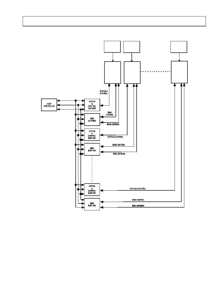
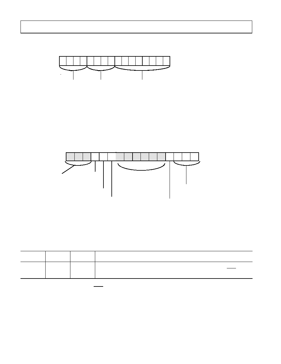
SYSTEM CONFIGURATION
Figure on page 9
shows the hardware interfaces for a typi-
cal multichannel modem configuration with the
ADSP-21mod980N. Other system design considerations
such as host processing requirements, electrical loading,
and overall bus timing must all be met. A line interface can
be used to connect the multichannel subscriber or client
data stream to the multichannel serial port of the
ADSP-21mod980N. The IDMA port of the
ADSP-21mod980N is used to give a host processor full
access to the internal memory of the ADSP-21mod980N.
This lets the host dynamically configure the
ADSP-21mod980N by loading code and data into its inter-
nal memory. This configuration also lets the host access
server data directly from the ADSP-21mod980N's internal
memory. In this configuration, the Modem Processors
should be put into host memory mode where Mode C = 1,
Mode B = 0, and Mode A = 1.
9
REV. PrB
6/2001
For current information contact Analog Devices at (800) ANALOGD
ADSP-21mod980N
PRELIMINARY TECHNICA L DATA
CLOCK SIGNALS
The ADSP-21mod980N is clocked by a TTL-compatible
clock signal that runs at half the instruction rate; a 40 MHz
input clock yields a 12.5 ns processor cycle, which is equiv-
alent to 80 MHz. Normally, instructions are executed in a
single processor cycle. All device timing is relative to the
internal instruction clock rate, which is indicated by the
CLKOUT signal when enabled. The clock input signal is
connected to the processor's CLKIN input.
The CLKIN input cannot be halted, changed during oper-
ation, or operated below the specified frequency during
normal operation. The only exception is while the processor
is in the power down state. For additional information, refer
to Chapter 9, ADSP-2100 Family User's Manual for a
detailed explanation of this power down feature.
Figure 3. Multichannel Modem Configuration
SPORT
21mod980N
ST/CNTL IDMA
SPORT
21mod980N
ST/CNTL IDMA
21mod980N
ST/CNTL IDMA
T1/E1
LINE
INTERFACE
SPORT
T1/E1
LINE
INTERFACE
T1/E1
LINE
INTERFACE
10
6/2001 REV. PrB
For current information contact Analog Devices at (800) ANALOGD
ADSP-21mod980N
PRELIMINARY TECHNICAL DATA
A clock output (CLKOUT) signal is generated by the pro-
cessor at the processor's cycle rate. This can be enabled and
disabled by the CLKODIS bit in the SPORT0 Autobuffer
Control Register.
RESET
The RESET signals initiate a reset of each modem proces-
sor in the ADSP-21mod980N. The RESET signals must be
asserted during the power-up sequence to assure proper ini-
tialization. RESET during initial power-up must be held
long enough to let the internal clocks stabilize. If RESETs
are activated any time after power up, the clocks continue to
run and do not require stabilization time.
The power-up sequence is defined as the total time required
for the oscillator circuits to stabilize after a valid V
DD
is
applied to the processors, and for the internal phase-locked
loops (PLL) to lock onto the specific frequency. A mini-
mum of 2000 CLKIN cycles ensures that the PLLs have
locked, but this does not include the oscillators' start-up
time. During this power-up sequence, the RESET signals
should be held low. On any subsequent resets, the RESET
signals must meet the minimum pulse width specification,
t
RSP
.
The RESET input contains some hysteresis; however, if you
use an RC circuit to generate your RESET signals, the use
of an external Schmidt triggers are recommended.
The RESET for each individual modem processor sets the
internal stack pointers to the empty stack condition, masks
all interrupts and clears the MSTAT register. When a
RESET is released, if there is no pending bus request and
the modem processor is configured for booting, the
boot-loading sequence is performed. The first instruction is
fetched from on-chip program memory location 0x0000
once boot loading completes.
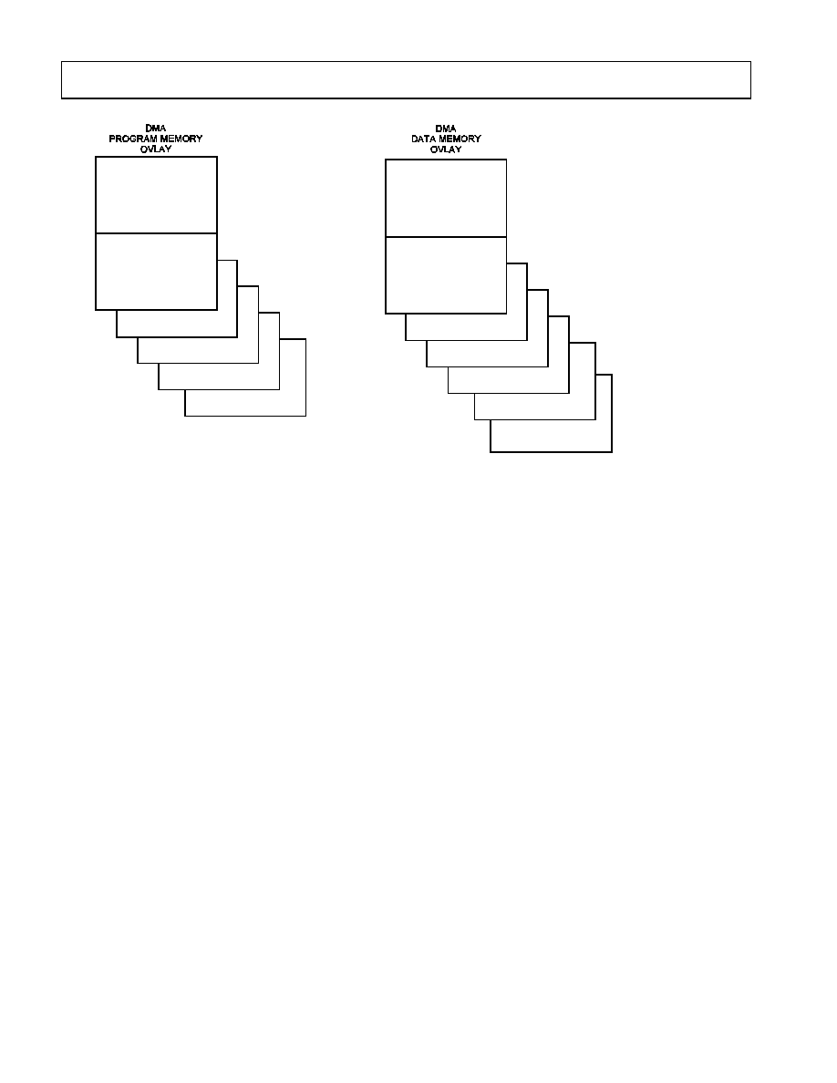
MEMORY ARCHITECTURE
The ADSP-21mod980N provides a variety of memory and
peripheral interface options for Modem Processor 1. The
key functional groups are Program Memory, Data Memory,
Byte Memory, and I/O. Refer to the following figures and
tables for PM and DM memory allocations in the
ADSP-21mod980N.
The ADSP-21mod980N modem pool operates in one
memory mode: Slave Mode. The following figures and
tables describe the memory of the ADSP-21mod980N:
·
Figure on page 10
shows Program Memory
·
Table on page 10
shows the generation of address bits
based on the PMOVLAY values
·
Figure on page 11
shows Data Memory
·
Table on page 11
shows the generation of address bits
based on the DMOVLAY values. Access to external
memory is not available
Figure 4. Program Memory Map
Table 4. PMOVLAY bits
PMOVLAY
Memory
A13
A[12:0]
0, 4, 5, 6, 7
Internal
Not
Applicable
Not Applicable
0 x 2 0 0 0 -
0 x 3 F F F
A C C E S S IB L E
W H E N
P M O V L A Y = 7
0 x 2 0 0 0 -
0 x 3 F F F
A C C E S S IB L E
W H E N
P M O V L A Y = 6
0 x 2 0 0 0 -
0 x 3 F F F
A C C E S S IB L E W H E N
P M O V L A Y = 5
P M O V L A Y = 0
A C C E S S IB L E W H E N
0 x 2 0 0 0 -
0 x 3 F F F
0 x 2 0 0 0 -
0 x 3 F F F
A C C E S S IB L E W H E N
P M O V L A Y = 4
P M M O D E B = 0
A L W A Y S
A C C E S S IB L E
A T A D D R E S S
0 x 0 0 0 0 - 0 x 1 F F F
0x3FFF
8K
INTERNAL
0x0000
8K INTERNAL
PMOVLAY =
0, 4, 5, 6, 7
0x1FFF
0x2000
PROGRAM MEMORY
MODE B=0
ADDRESS
IN T E R N A L
M E M O R Y
11
REV. PrB
6/2001
For current information contact Analog Devices at (800) ANALOGD
ADSP-21mod980N
PRELIMINARY TECHNICAL DATA
MEMORY MAPPED REGISTERS (NEW TO THE
ADSP-21MOD980N)
The ADSP-21mod980N has three memory mapped regis-
ters that differ from other ADSP-21xx Family DSPs. See
"Waitstate Control Register" on page 11. See
"Programmable Flag & Composite Select Control Regis-
ter" on page 12. See "System Control Register" on
page 12. The slight modifications to these registers provide
the ADSP-21mod980N's waitstate and BMS control
features.
Figure 5. Data Memory Map
A C C E SS IB L E W H EN
D M O VL A Y = 8
0 x 00 0 0 - 0 x 1F F F
A C C E SS IB L E W H EN
D M O VL A Y = 7
0 x 00 0 0 - 0 x 1F F F
A C C E SS IB L E W H EN
D M O VL A Y = 6
32 MEMORY
MAPPED
REGISTERS
0x3FFF
INTERNAL
8160 WORDS
DATA MEMORY
ADDR
0x3FE0
8K INTERNAL
DMOVLAY =
0, 4, 5, 6, 7, 8
0x1FFF
0x3FDF
0x2000
A C C E SS IB L E W H EN
D M O VL A Y = 5
A C C E SS IB L E W H EN
D M O VL A Y = 4
0 x 00 0 0 - 0 x 1F F F
A C C E SS IB L E W H EN
D M O VL A Y = 0
0 x 00 0 0 - 0 x 1F F F
0 x 00 0 0 - 0 x 1F F F
D A T A M EM O R Y
A L W A Y S
A C C E SS IB L E
A T A D D R E S S
0 x 20 0 0 - 0 x 3F F F
IN T ER N A L
M E M O R Y
0 x 00 0 0 - 0 x 1F F F
Table 5. DMOVLAY bits
DMOVLAY
Memory
A13
A[12:0]
0, 4, 5, 6, 7, 8
Internal
Not
Applicable
Not
Applicable
.
Figure 6. Waitstate Control Register
15
14
13
12
11
10
9
8
7
6
5
4
3
2
1
0
1
1
1
1
1
1
1
1
1
1
1
1
1
1
1
1
IO W AIT 0
W ait State M od e Select
0 = Norm al m od e (P W AIT , DW AIT , IO W AIT 0-3 = N w ait states, rang ing fro m 0 to 7)
1 = 2N+ 1 m ode (P W AIT , D W AIT , IO W AIT 0-3 = 2N +1 w ait states, rang ing from 0 to 15)
DM (0x3FF E)
IO W AIT 1
IO W AIT 2
IO W AIT 3
DW AIT
12
6/2001 REV. PrB
For current information contact Analog Devices at (800) ANALOGD
ADSP-21mod980N
PRELIMINARY TECHNICAL DATA
SLAVE MODE
This section describes the Slave Mode memory configura-
tion of the Modem Processors.
INTERNAL MEMORY DMA PORT (IDMA PORT)
The IDMA Port provides an efficient way for a host system
and the ADSP-21mod980N to communicate. The port is
used to access the on-chip program memory and data mem-
ory of each modem processor with only one processor cycle
per word overhead. The IDMA port cannot be used, how-
Figure 7. Programmable Flag
1
& Composite Select Control Register
1
Since they are multiplexed within the ADSP-21mod980N, PF[2:0] should be configured as an output for only one processor at a time. Bit [3] of DM
(0x3FE6) must also be 0 to ensure that PF[3] is never an output.
15 14 13 12 11 10 9
8
7
6
5
4
3
2
1
0
1
1
1
1
1
0
1
1
0
0
0
0
0
0
0
0
DM(0x3FE6)
PFTYPE
0 = Input
1 = Output
CMSSEL
0 = Disable CMS
1 = Enable CMS
(where bit: 11-IOM, 10-BM, 9-DM, 8-PM)
BMWAIT
Figure 8. System Control Register
15
14
13
12
11
10
9
8
7
6
5
4
3
2
1
0
0
0
0
0
0
1
0
0
0
1
1
1
0
0
0
0
SPO RT 1 En ab le
0 = Disable
1 = Enable
PW AIT
Pro gram M em ory
W ait S tates
SPO R T 1 Configu re
0 = F I, F O , IR Q 0, IRQ 1, SCL K
1= SPO RT 1
Disab le B M S
0 = En able B M S
1 = D isable B M S , excep t w hen
m em ory strobes are three-stated
SPO RT 0 En ab le
0 = Disable
1 = Enable
DM (0x3F FF )
RE S ER V E D
SET T O 0
Reserved Set
T o 0
Table 6. ADSP-21mod980N Mode of Operation
MODE C
MODE B
MODE A
Booting Method
1
0
1
IDMA feature is used to load internal memory as desired. Program execution is held off until internal
program memory location 0x0000 is written to. Chip is configured in Slave Mode.
1
IACK requires
external pulldown.
2
1
Considered standard operating settings. These configurations simplify your design and improve memory management.
2
IDMA timing details and the correct usage of IACK are described in the ADSP-2100 Family User's Manual.
13
REV. PrB
6/2001
For current information contact Analog Devices at (800) ANALOGD
ADSP-21mod980N
PRELIMINARY TECHNICAL DATA
ever, to write to the processor's memory-mapped control
registers. A typical IDMA transfer process is described as
follows:
1.
Host starts IDMA transfer
2.
Host uses IS and IAL control lines to latch either the
DMA starting address (IDMAA) or the PM/DM
OVLAY selection into the processor's IDMA control
registers.
If IAD [15] = 1, the value of IAD [7:0] represents the
IDMA overlay: IAD[14:8] must be set to 0.
If IAD [15] = 0, the value of IAD [13:0] represents the
starting address of internal memory to be accessed and
IAD [14] reflects PM or DM for access.
1.
Host uses IS and IRD (or IWR) to read (or write) pro-
cessor internal memory (PM or DM).
2.
Host ends IDMA transfer.
The IDMA port has a 16-bit multiplexed address and data
bus and supports 24-bit program memory. The IDMA port
is completely asynchronous and can be written to, while the
ADSP-21mod980N is operating at full speed.
The processor memory address is latched and then auto-
matically incremented after each IDMA transaction. An
external device can therefore access a block of sequentially
addressed memory by specifying only the starting address of
the block. This increases throughput as the address does
not have to be sent for each memory access.
IDMA Port access occurs in two phases. The first is the
IDMA Address Latch cycle. When the acknowledge is
asserted, a 14-bit address and 1-bit destination type can be
driven onto the bus by an external device. The address
specifies an on-chip memory location, the destination type
specifies whether it is a DM or PM access. The falling edge
of the address latch signal latches this value into the
IDMAA register.
Once the address is stored, data can then be either read
from, or written to, the ADSP-21mod980N's on-chip
memory. Asserting the select line (IS) and the appropriate
read or write line (IRD and IWR respectively) signals the
ADSP-21mod980N that a particular transaction is
required. In either case, there is a one-processor-cycle delay
for synchronization. The memory access consumes one
additional processor cycle.
Once an access has occurred, the latched address is auto-
matically incremented, and another access can occur.
Through the IDMAA register, the processor can also spec-
ify the starting address and data format for DMA operation.
Asserting the IDMA port select (IS) and address latch
enable (IAL) directs the ADSP-21mod980N to write the
address onto the IAD [14:0] bus into the IDMA Control
Register. If IAD [15] is set to 0, IDMA latches the address.
If IAD [15] is set to 1, IDMA latches OVLAY memory. The
IDMAA register is memory mapped at address DM
(0x3FE0). Note that the latched address (IDMAA) or over-
lay register cannot be read back by the host. The IDMA
OVERLAY register is memory mapped at address
DM(0x3FE7). See
Figure on page 13
for more informa-
tion on IDMA memory mapping. When bit 14 in 0x3FE7
is set to 1, then timing in
Figure on page 35
applies for
short reads. When bit 14 in 0x3FE7 is set to zero short
reads use the timing shown in
Figure on page 34
.
Figure 9. IDMA Control/OVLAY Registers
15
14
13
12
11
10
9
8
7
6
5
4
3
2
1
0
IDM A O VER LAY
DM (0x3FE7)
ID DM OVLAY
ID PM O VLAY
RESERVE D
SET TO 0
15
14
13
12
11
10
9
8
7
6
5
4
3
2
1
0
IDM A CO NTRO L (U=U NDEF INED AT R ESET)
U
DM (0x3FE0)
IDM AA
ADDR ESS
IDM AD
Destination m em ory type:
0=PM
1=DM
U
U
U
U
U
U
U
U
U
U
U
U
U
U
Short R ead Only
En able
1 = Enable
0 = D isable
0
0
0
0
0
0
0
0
0
0
0
0
0
0
0
0
0
RESE RVED
ALW A YS SET
TO 0
RESE RVED
ALW A YS SET
TO 0
14
6/2001 REV. PrB
For current information contact Analog Devices at (800) ANALOGD
ADSP-21mod980N
PRELIMINARY TECHNICAL DATA
Figure 10. Direct Memory Access - PM and DM Memory Maps
AC CE SSIBLE W H E N
DM O VLAY = 8
AC CE SSIBLE W H E N
DM O VLAY = 7
0x0000 - 0x 1FFF
0x0000 - 0x 1FF F
AC CE SSIBLE W H E N
PM O VLAY = 7
0x2000 - 0x 3FFF
AC CE SSIBLE W H E N
PM O VLAY = 6
AC CE SSIBLE W H EN
PM O VLAY = 5
AC CE SSIBLE W H E N
PM O VLAY = 4
0x2000 - 0x 3FF F
AC CE SS IBLE W H EN
PM O VLAY = 0
0x20 00 - 0x 3FF F
0x2000 - 0x 3FFF
ALW A YS
AC CE S SIBLE
AT AD DR ESS
0x0000 - 0x 1FFF
0x2000 - 0x 3FF F
AC CE SSIBLE W H E N
DM O VLAY = 6
AC CE SS IBLE W H E N
DM O VLAY = 5
AC CE SSIBLE W H E N
DM O VLAY = 4
0x0000 - 0x 1FF F
AC CE SSIBLE W H E N
DM O VLAY = 0
0x0000 - 0x 1FF F
0x0000 - 0x 1FF F
ALW A Y S
AC CE S SIB LE
AT A D DR ESS
0x2000 - 0x 3FFF
0x00 00 - 0x 1FF F

15
REV. PrB
6/2001
For current information contact Analog Devices at (800) ANALOGD
ADSP-21mod980N
PRELIMINARY TECHNICAL DATA
IDMA PORT BOOTING
The ADSP-21mod980N boots programs through its Inter-
nal DMA port.When Mode C = 1, Mode B = 0, and Mode
A = 1, the ADSP-21mod980N boots from the IDMA port.
IDMA feature can load as much on-chip memory as
desired. Program execution is held off until on-chip pro-
gram memory location 0 is written to.
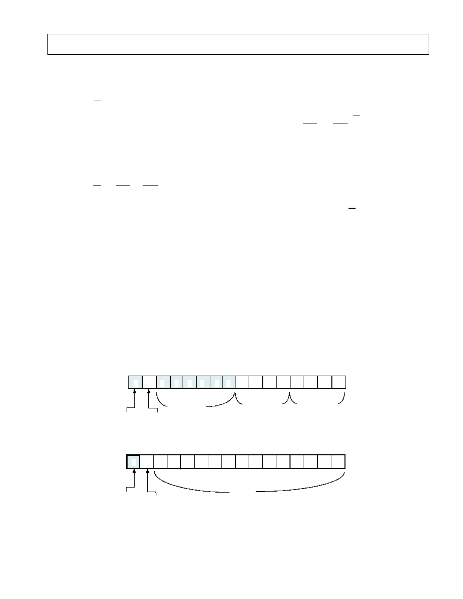
FLAG I/O PINS
Each modem processor has eight general purpose program-
mable input/output flag pins. They are controlled by two
memory mapped registers. The PFTYPE register deter-
mines the direction, 1 = output and 0 = input. The
PFDATA register is used to read and write the values on the
pins. Data being read from a pin configured as an input is
synchronized to the ADSP-21mod980N's clock. Bits that
are programmed as outputs will read the value being out-
put. The PF pins default to input during RESET.
Note: Pins PF0, PF1, and PF2 are also used for device con-
figuration during RESET. Since they are multiplexed
within the ADSP-21mod980N, PF[2:0] should be config-
ured as an output for only one processor at a time.
16
6/2001 REV. PrB
For current information contact Analog Devices at (800) ANALOGD
ADSP-21mod980N
PRELIMINARY TECHNICAL DATA
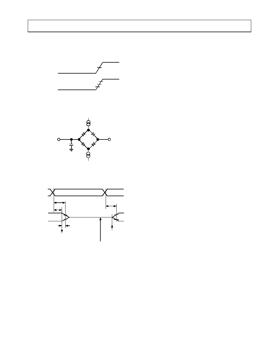
DESIGNING AN EZ-ICE-COMPATIBLE SYSTEM
The ADSP-21mod980N has on-chip emulation support
and an ICE-Port, a special set of pins that interface to the
EZ-ICE. These features allow in-circuit emulation without
replacing the target system processor by using only a 14-pin
connection from the target system to the EZ-ICE. Target
systems must have a 14-pin connector to accept the
EZ-ICE's in-circuit probe, a 14-pin plug.
The EZ-ICE can emulate only one modem processor at a
time. You must include hardware to select which processor
in the ADSP-21mod980N you want to emulate.
Figure on
page 16
is a functional representation of the modem proces-
sor selection hardware. You can use one ICE-Port
connector with two ADSP-21mod980N processors without
using additional buffers.
Issuing the "chip reset" command during emulation causes
the modem processor to perform a full chip reset, including
a reset of its memory mode. Therefore, it is vital that the
mode pins are set correctly PRIOR to issuing a chip reset
command from the emulator user interface. As the mode
pins share functionality with PF[2:0] on the
Figure 11. Selecting a Modem Processor in the ADSP-21mod980N
1
2
3
4
5
6
7
8
9
10
11
12
13
14
BG
BR
E NT
E L IN
E CL K
E M S
E RE S E T
G ND
E BG
E BR
KE Y
E L O U T
E E
RE S E T
BG 6
BR 6
RE S E T 6
E E 6
BG 7
BR 7
RE S E T 7
E E 7
BG 5
BR 5
RE S E T 5
E E 5
BG 4
BR 4
RE S E T 4
E E 4
BG 3
BR 3
RE S E T 3
E E 3
BG 2
BR 2
RE S E T 2
E E 2
BG 1
BR 1
RE S E T 1
E E 1
BG 0
BR 0
RE S E T 0
E E 0
E L O U T
E BR
E BG
E INT
E L IN
E CL K
E M S
E RE S E T
A D S P-21 M O D980N
17
REV. PrB
6/2001
For current information contact Analog Devices at (800) ANALOGD
ADSP-21mod980N
PRELIMINARY TECHNICAL DATA
ADSP-21mod980N, it may be necessary to reset the target
hardware separately to insure the proper mode selection
state on emulator chip reset. See the ADSP-2100 Family
EZ-Tools data sheet for complete information on ICE
products.
The ICE-Port interface consists of the following
ADSP-21mod980N pins:
EBR
EINT
EE
EBG
ECLK
ERESET
ELIN
EMS
ELOUT
These ADSP-21mod980N pins must be connected only to
the EZ-ICE connector in the target system. These pins have
no function except during emulation, and do not require
pull-up or pull-down resistors. The traces for these signals
between the ADSP-21mod980N and the connector must
be kept as short as possible--no longer than 3 inches.
The following pins are also used by the EZ-ICE:
·
BR
·
BG
·
RESET
·
GND
The EZ-ICE uses the EE (emulator enable) signal to take
control of the ADSP-21mod980N in the target system.
This causes the processor to use its ERESET, EBR, and
EBG pins instead of the RESET, BR, and BG pins. The BG
output is three-stated. These signals do not need to be
jumper-isolated in your system.
The EZ-ICE connects to your target system via a ribbon
cable and a 14-pin female plug. The female plug is plugged
onto the 14-pin connector (a pin strip header) on the target
board.
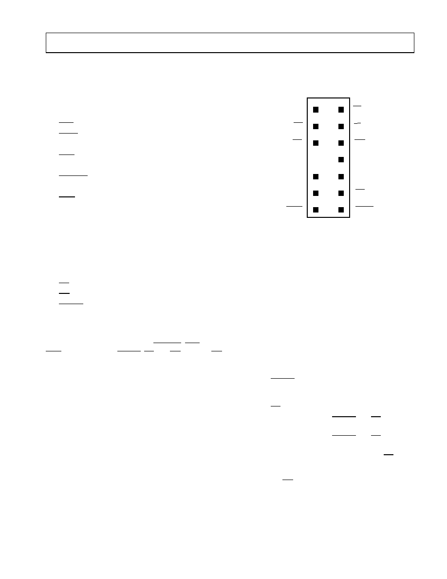
TARGET BOARD CONNECTOR FOR EZ-ICE PROBE
The EZ-ICE connector (a standard pin strip header) is
shown in
Figure on page 17
. You must add this connector
to your target board design if you intend to use the EZ-ICE.
Be sure to allow enough room in your system to fit the
EZ-ICE probe onto the 14-pin connector.
The 14-pin, 2-row pin strip header is keyed at the Pin 7
location--you must remove Pin 7 from the header. The pins
must be 0.025 inch square and at least 0.20 inch in length.
Pin spacing should be 0.1 0.1 inches. The pin strip
header must have at least 0.15 inch clearance on all sides to
accept the EZ-ICE probe plug.
Pin strip headers are available from vendors such as 3M,
McKenzie, and Samtec.
TARGET MEMORY INTERFACE
For your target system to be compatible with the EZ-ICE
emulator, it must comply with the memory interface guide-
lines listed below.
TARGET SYSTEM INTERFACE SIGNALS
When the EZ-ICE board is installed, the performance on
some system signals change. Design your system to be com-
patible with the following system interface signal changes
introduced by the EZ-ICE board:
·
EZ-ICE emulation introduces an 8 ns propagation
delay between your target circuitry and the processor
on the RESET signal.
·
EZ-ICE emulation introduces an 8 ns propagation
delay between your target circuitry and the processor
on the BR signal.
·
EZ-ICE emulation ignores RESET and BR when
single-stepping.
·
EZ-ICE emulation ignores RESET and BR when in
Emulator Space (processor halted).
·
EZ-ICE emulation ignores the state of target BR in cer-
tain modes. As a result, the target system may take
control of the processor's external memory bus only if
bus grant (BG) is asserted by the EZ-ICE board's
processor.
Figure 12. Target Board Connector for EZ-ICE
1
2
3
4
5
6
7
8
9
10
11
12
13
14
GN D
KEY (N O PIN)
R E S E T
B R
B G
TOP VIEW
EBG
EBR
ELOUT
EE
EINT
ELIN
ECLK
EMS
ERESET

18
6/2001 REV. PrB
For current information contact Analog Devices at (800) ANALOGD
ADSP-21mod980N
PRELIMINARY TECHNICAL DATA
ELECTRICAL SPECIFICATIONS
RECOMMENDED OPERATING CONDITIONS
Parameter
Description
Min
Max
Unit
V
DDEXT
External supply
2.98
3.63
V
V
DDINT
Internal supply
1.81
2.0
V
V
INPUT
Input Voltage
V
IL
= 0.3
V
IH
= +3.6
V
T
AMB
Ambient temperature
0
+70
°
C
ELECTRICAL CHARACTERISTICS
Parameter
Test Conditions
Min
Typ
Max
Unit
V
IH
, Hi-Level Input Voltage
1, 2
@ V
DDINT
= max
1.5
V
V
IH
, Hi-Level CLKIN Voltage
@ V
DDINT
= max
2.0
V
V
IL
, Lo-Level Input Voltage
1, 3
@ V
DDINT
= min
0.7
V
V
OH
, Hi-Level Output Voltage
1, 4, 5
@ V
DDEXT
= min
I
OH
= 0.5 mA
2.4
V
@ V
DDEXT
= min
I
OH
= 100 µA
6
V
DDEXT
-0.3
V
V
OL
, Lo-Level Output Voltage
1, 4, 5
@ V
DDEXT
= min
I
OL
= 2 mA
0.4
V
I
IH
, Hi-Level Input Leakage Current
3
@ V
DDINT
= max
V
IN
= 3.6V
10
A
I
IL
, Lo-Level Input Leakage Current
3
@ V
DDINT
= max
V
IN
= 0 V
10
A
I
OZH
, Three-State Leakage Current
7
@ V
DDEXT
= max
V
IN
= 3.6V
8
10
A
I
OZL
, Three-State Leakage Current
7
@ V
DDEXT
= max
V
IN
= 0 V
8
10
A

19
REV. PrB
6/2001
For current information contact Analog Devices at (800) ANALOGD
ADSP-21mod980N
PRELIMINARY TECHNICAL DATA
I
DD
, Supply Current (Idle)
@ V
DDINT
= 1.9V
t
CK
= 12.5 ns
50
mA
I
DD
, Supply Current (Dynamic)
@ V
DDINT
= 1.9V
t
CK
= 12.5 ns
9
T
AMB
= +25°C
200
mA
I
DD
, Supply Current (Powerdown)
10
Lowest power mode
800
µA
C
I
, Input Pin Capacitance
RESET, BR, IS, TFS0, PF[7:4]
@ V
IN
= 2.5 V, f
IN
= 1.0 MHz,
T
AMB
= +25°C
8
pF
C
I
, Input Pin Capacitance
IWR
,
IRD, IAL, DR0, RFS0, SCLK0, IAD [15:0]
@ V
IN
= 2.5 V, f
IN
= 1.0 MHz,
T
AMB
= +25°C
32
pF
C
I
, Input Pin Capacitance
TFS1, PF[2:0], CLKIN, DR1, RFS1, SCLK1
@ V
IN
= 2.5 V, f
IN
= 1.0 MHz,
T
AMB
= +25°C
64
pF
C
O
, Output Pin Capacitance
1, 6, 7, 10, 11
BG, CLKOUT, TFS0, PF[7:4], DT1
@ V
IN
= 2.5 V, f
IN
= 1.0 MHz,
T
AMB
= +25°C
8
pF
C
O
, Output Pin Capacitance
1, 6, 7, 9, 10
IAD [15:0]
,
DT0, IACK, RFS0, SCLK0
@ V
IN
= 2.5 V, f
IN
= 1.0 MHz,
T
AMB
= +25°C
32
pF
C
O
, Output Pin Capacitance
1, 6, 7, 9, 10
SCLK1, TFS1, PF[2:0], DATA [23:8], A0, RFS1
@ V
IN
= 2.5 V, f
IN
= 1.0 MHz,
T
AMB
= +25°C
64
pF
1
Bidirectional pins: RFS0, RFS1, SCLK0, SCLK1, TFS0, TFS1, IAD [15:0], PF[2:0], PF[7:4].
2
Input only pins: RESET, BR, DR0, DR1, IS, IAL,IRD, IWR.
3
Input only pins: CLKIN, RESET, BR, DR0, DR1.
4
Output pins: BG, A0, DT0, DT1, CLKOUT, IACK.
5
Although specified for TTL outputs, all ADSP-21mod980N outputs are CMOS-compatible and will drive to V
DDEXT
and GND, assuming no DC
loads.
6
Guaranteed but not tested.
7
Three-statable pins: DT0, DT1, SCLK0, SCLK1, TFS0, TFS1, RFS0, RSF1, IAD[15:0].
8
0 Volts on BR.
9
Vin = 0V and 3V. For typical supply current figures refer to "Power Dissipation" section.
10
See the ADSP-2100 Family User's Manual for details.
11
Output pin capacitance is the capacitive load for any three-stated output pin
ELECTRICAL CHARACTERISTICS (CONTINUED)
Parameter
Test Conditions
Min
Typ
Max
Unit
20
6/2001 REV. PrB
For current information contact Analog Devices at (800) ANALOGD
ADSP-21mod980N
PRELIMINARY TECHNICAL DATA
ABSOLUTE MAXIMUM RATINGS
Parameter
Description
Min.
Max
Unit
V
DDINT
Internal Supply Voltage
0.3
+2.5
V
V
DDEXT
External Supply Voltage
0.3
+4.6
V
Input Voltage
1
0.5
+4.6
V
Output Voltage Swing
2
0.5
V
DDEXT
+ 0.5
V
Storage Temperature Range
65 °C
+150 °C
°C
1
Applies to bidirectional pins (D0:D23, RFS0, RFS1, SCLK0, SCLK1, TFS0, TFS1, A1:A13, PF0:PF7) and input only pins (CLKIN, RESET, BR,
DR0, DR1).
2
Applies to output pins (BG, PWDACK, A0, DT0, DT1, CLKOUT).
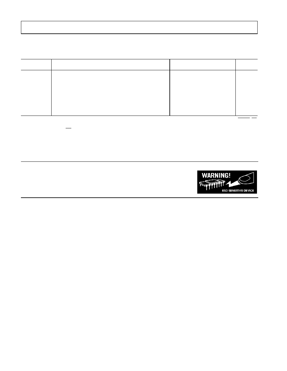
ESD SENSITIVITY
CAUTION: ESD (electrostatic discharge) sensitive device. Electrostatic charges as high
as 4000V readily accumulate on the human body and test equipment and can discharge
without detection. Although the device features proprietary ESD protection circuitry,
permanent damage may occur on devices subjected to high-energy electrostatic dis-
charges. Therefore, proper ESD precautions are recommended to avoid performance
degradation or loss of functionality.

21
REV. PrB
6/2001
For current information contact Analog Devices at (800) ANALOGD
ADSP-21mod980N
PRELIMINARY TECHNICAL DATA
POWER DISSIPATION
To determine total power dissipation in a specific applica-
tion, the following equation should be applied for each
output:
C V
DD
2
f
C = load capacitance
f = output switching frequency
Example:
In an application where an external host is accessing inter-
nal memory and no other outputs are active, power
dissipation is calculated as follows:
Assumptions:
Assumptions:
·
External data memory is accessed every fourth cycle
with 50% of the address pins switching.
·
External data memory writes occur every fourth cycle
with 50% of the data pins switching.
·
Each address and data pin has a 64 pF total load at the
pin.
·
Application operates at V
DDEXT
= 3.3 V and t
CK
= 30 ns.
Total Power Dissipation = P
INT
+ (C V
DDEXT
2
f)
P
INT
= internal power dissipation from
Figure 15
(C V
DDEXT
2
f) is calculated for each output, as in the
example in
Table 7
.
Total power dissipation for this example is:
PD = P
INT
+ 222.7 mW
Table 7. Example Power Dissipation Calculation
Parameters
# of Pins
× C (pF)
× V
DDEXT
2
(V)
× f (MHz)
PD (mW)
Address
8
64
3.3
2
18.8 104.8
Data Output, WR
9
64
3.3
2
18.8
117.9
222.7
22
6/2001 REV. PrB
For current information contact Analog Devices at (800) ANALOGD
ADSP-21mod980N
PRELIMINARY TECHNICAL DATA
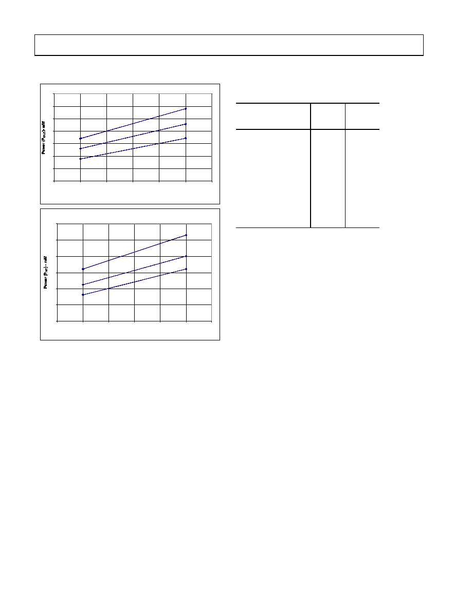
ENVIRONMENTAL CONDITIONS
Figure 13. Power vs. Frequency
M O D 9 80 N C o re P O W E R , ID L E
5 0
6 0
7 0
8 0
9 0
10 0
11 0
12 0
5 5
6 0
65
7 0
75
8 0
8 5
1/t
C K
- M Hz
V
D D
= 1 .8 v
1 0 8 m W
V
D D
= 1 .9 v
V
D D
= 2 .0 v
6 8 m W
7 6 m W
8 4 m W
9 6 m W
8 4 m W
M O D 9 8 0N C o r e P O W E R , D Y N A M IC
17 5
22 5
27 5
32 5
37 5
42 5
47 5
55
6 0
6 5
7 0
75
8 0
8 5
1/t
C K
- M Hz
V
D D
= 2 .0 V
V
D D
= 1 .9 V
2 8 7 m W
3 3 6 m W
3 7 5 m W
4 4 0 m W
3 3 6 m W
2 5 6 m W
V
D D
= 1 .8 V
Table 8. Thermal Resistance
Rating
Description
1
1
Where the Ambient Temperature Rating (T
AMB
) is:
T
AMB
= T
CASE
(PD ×
CA
)
T
CASE
= Case Temperature in
°
C
PD = Power Dissipation in W
Symbol
PBGA
Thermal Resistance
(Case-to-
Ambient)
CA
23ºC
/W
Thermal Resistance
(Junction-to-
Ambient)
JA
28.2ºC
/W
Thermal Resistance
(Junction-to-
Case)
JC
5.2ºC
/W
23
REV. PrB
6/2001
For current information contact Analog Devices at (800) ANALOGD
ADSP-21mod980N
PRELIMINARY TECHNICAL DATA
TEST CONDITIONS
Output Disable Time
Output pins are considered to be disabled when they have
stopped driving and started a transition from the measured
output high or low voltage to a high impedance state. The
output disable time (t
DIS
) is the difference of t
MEASURED
and
t
DECAY
, as shown in
Figure 16
. The time is the interval from
when a reference signal reaches a high or low voltage level
to when the output voltages have changed by 0.5 V from the
measured output high or low voltage.
The decay time, t
DECAY
, is dependent on the capacitive load,
C
L
, and the current load, i
L
, on the output pin. It can be
approximated by the following equation:
from which
is calculated. If multiple pins (such as the data bus) are dis-
abled, the measurement value is that of the last pin to stop
driving.
Output Enable Time
Output pins are considered to be enabled when they have
made a transition from a high-impedance state to when they
start driving. The output enable time (t
ENA
) is the interval
from when a reference signal reaches a high or low voltage
level to when the output has reached a specified high or low
trip point, as shown in
Figure 16
. If multiple pins (such as
the data bus) are enabled, the measurement value is that of
the first pin to start driving.
Figure 14. Voltage Reference Levels for AC
Measurements (Except Output Enable/Disable)
Figure 15. Equivalent Loading for AC Measurements
(Including All Fixtures)
Figure 16. Output Enable/Disable
1.5V
O UT P UT
IN P U T
1.5V
2.0V
0.8V
T O
O UT P UT
P IN
50p F
1.5V
I
O H
I
O L
2.0V
1.0V
t
E N A
RE F E RE NC E
S IG N AL
O UT P UT
t
DE CA Y
V
O H
(M E A S U R E D)
O UT P UT S TO P S
DR IV ING
O UT P UT S TA RT S
DR IV ING
t
DI S
t
M E A S UR E D
V
O L
(M E A S U R E D)
V
O H
(M E A S U RE D ) - 0.5V
V
O L
(M E A S U RE D ) +0.5V
HIG H-IM P E DAN CE S T AT E . T E S T CO ND IT IO N S CAU S E
T HIS V O LT AGE L E V E L T O B E AP P RO XIM AT E LY 1.5V .
V
O H
(M E A S U R E D)
V
O L
(M E A S U R E D)
t
DECAY
C
L
0.5V
×
i
L
-------------------------
=
t
DIS
t
MEASURED
t
DECAY
=

24
6/2001 REV. PrB
For current information contact Analog Devices at (800) ANALOGD
ADSP-21mod980N
PRELIMINARY TECHNICAL DATA
TIMING SPECIFICATIONS
This section contains timing information for the DSP's
external signals.
General Notes
Use the exact timing information given. Do not attempt to
derive parameters from the addition or subtraction of oth-
ers. While addition or subtraction would yield meaningful
results for an individual device, the values given in this data
sheet reflect statistical variations and worst cases. Conse-
quently, you cannot meaningfully add up parameters to
derive longer times.
Timing Notes
Switching characteristics specify how the processor changes
its signals. You have no control over this timing--circuitry
external to the processor must be designed for compatibility
with these signal characteristics. Switching characteristics
tell you what the processor will do in a given circumstance.
You can also use switching characteristics to ensure that any
timing requirement of a device connected to the processor
(such as memory) is satisfied.
Timing requirements apply to signals that are controlled by
circuitry external to the processor, such as the data input for
a read operation. Timing requirements guarantee that the
processor operates correctly with other devices.
Frequency Dependency For Timing Specifications
t
CK
is defined as 0.5 t
CKI
. The ADSP-21mod980N uses an
input clock with a frequency equal to half the instruction
rate. For example, a 40 MHz input clock (which is equiva-
lent to 25 ns) yields a 12.5 ns processor cycle (equivalent to
80 MHz). t
CK
values within the range of 0.5 t
CKI
period
should be substituted for all relevant timing parameters to
obtain the specification value.
Example: t
CKH
= 0.5 t
CK
2 ns = 0.5 (12.5 ns) 2 ns = 4.25
ns
Output Drive Currents
Figure 14
shows typical I-V characteristics for the output
drivers on the ADSP-21mod980N. The curves represent
the current drive capability of the output drivers as a func-
tion of output voltage
Capacitive Loading
Figure 16
and
Figure 17
show the capacitive loading char-
acteristics of the ADSP-21mod980N.
Figure 17. Typical Output Rise Time vs.Load Capacitance
(at Maximum Ambient Operating Temperature)
Figure 18. Typical Output Valid Delay or Hold vs.Load
Capacitance, CL (at Maximum Ambient Operating
Temperature)
C
L
- p F
RI
SE T
IM
E
(0
.
4
V
-
2.
4
V
)
- n
s
30
300
0
50
100
150
200
250
25
15
10
5
0
20
T = 85 C
V
D D
= 0V T O 2.0V
C
L
- p F
14
0
VA
LI
D
OU
T
PU
T
DE
LA
Y
OR
HO
L
D -
ns
50
100
150
250
200
12
4
2
-2
10
8
N OM IN AL
16
18
6
-4
-6

25
REV. PrB
6/2001
For current information contact Analog Devices at (800) ANALOGD
ADSP-21mod980N
PRELIMINARY TECHNICAL DATA
Clock and Reset Signals
Table 9. Clock and Reset Signals
Parameter
Description
Min.
Max
Unit
Clock signals (Timing Requirements):
t
CKI
CLKIN Period
25.0
40.0
ns
t
CKIL
CLKIN Width Low
8
ns
t
CKIH
CLKIN Width High
8
ns
t
CKRISE
CLKIN rise time
1
4
ns
t
CKFALL
CLKIN fall time
4
ns
Clock signals (Switching Characteristics)
2
:
t
CKL
CLKOUT Width Low
0.5t
CK
- 3
ns
t
CKH
CLKOUT Width High
0.5t
CK
- 3
ns
t
CKOH
CLKIN High to CLKOUT High
0
8
ns
Control Signals (Timing Requirements):
t
RSP
RESET Width Low
5t
CK
3
ns
t
MS
Mode Setup Before RESET High
4
ns
t
MH
Mode Hold After RESET High
5
ns
1
t
CKRISE
and t
CKFALL
are specified between the 10% and 90% points on the signal edge.
2
If it is not needed by the application, CLKOUT should be disabled to reduce noise (DM(0x3FF3) bit 14).
3
Applies after power-up sequence is complete. Internal phase lock loop requires no more than 2000 CLKIN cycles assuming stable CLKIN (not including
crystal oscillator start-up time).
26
6/2001 REV. PrB
For current information contact Analog Devices at (800) ANALOGD
ADSP-21mod980N
PRELIMINARY TECHNICAL DATA
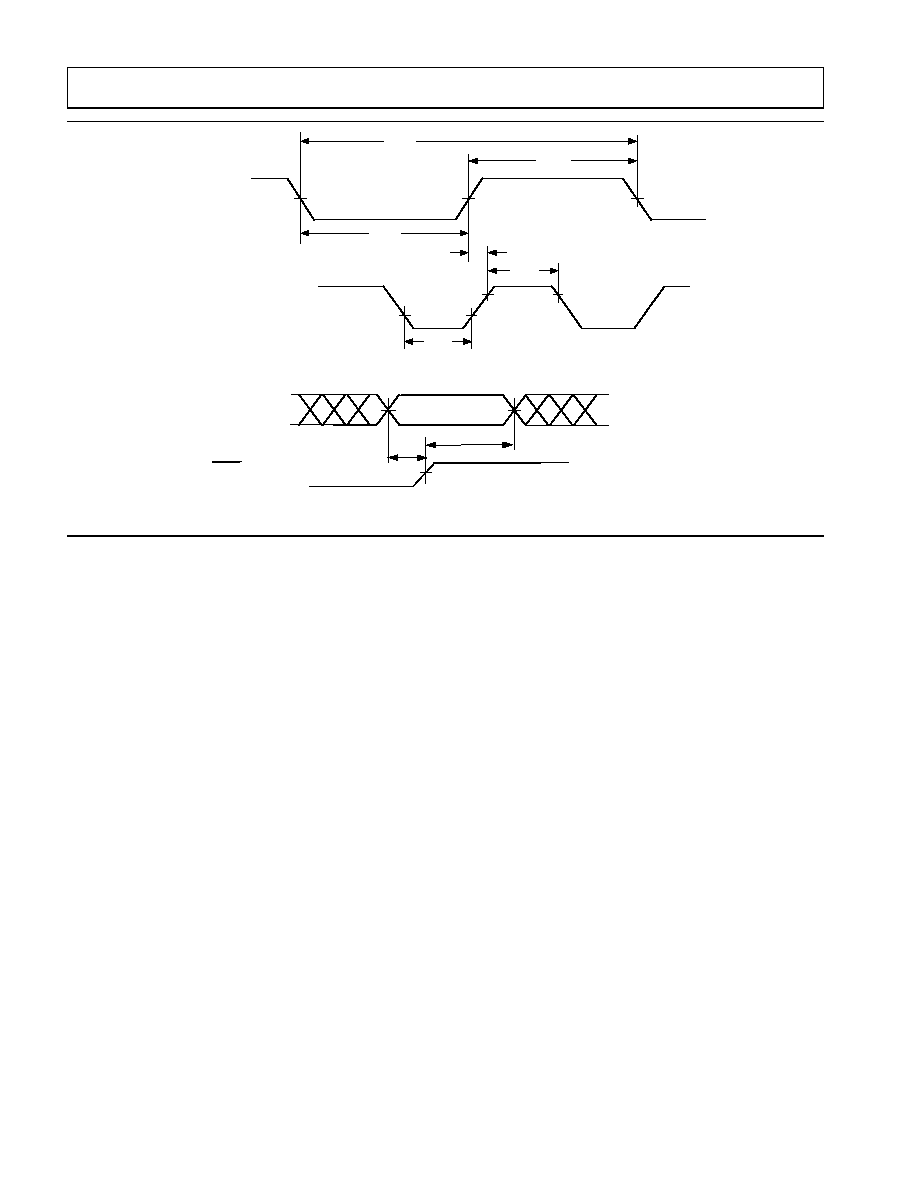
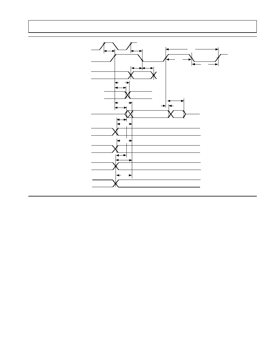
Figure 19. Clock and Reset Signals
t
MH
PF (2:0 )*
RE S E T
t
MS
*PF 2 is M ode C , PF 1 is M ode B, PF 0 is M ode A
CL K IN
CL K O U T
t
C K I L
t
C K O H
t
C K H
t
C K L
t
C K I
t
C K I H
27
REV. PrB
6/2001
For current information contact Analog Devices at (800) ANALOGD
ADSP-21mod980N
PRELIMINARY TECHNICAL DATA
Interrupts and Flags
Table 10. Interrupts and Flags
Parameter
Description
Min.
Max
Unit
Timing Requirements:
t
IFS
IRQx, FI, or PFx Setup before CLKOUT Low
1,
2, 3, 4
0.25t
CK
+ 10
ns
t
IFH
IRQx, FI, or PFx Hold after CLKOUT High
1, 2, 3, 4
0.25t
CK
ns
Switching Characteristics:
t
FOH
Flag Output Hold after CLKOUT Low
5
0.5t
CK
- 5
ns
t
FOD
Flag Output Delay from CLKOUT Low
5
0.5t
CK
+ 4
ns
1
If IRQx and FI inputs meet t
IFS
and t
IFH
setup/hold requirements, they will be recognized during the current clock cycle; otherwise the signals will be
recognized on the following cycle. (Refer to Interrupt Controller Operation in the Program Control chapter of the ADSP-2100 Family User's Manual for
further information on interrupt servicing.)
2
Edge-sensitive interrupts require pulse widths greater than 10 ns; level-sensitive interrupts must be held low until serviced.
3
IRQx = IRQ0, IRQ1, IRQ2, IRQL0, IRQL1, IRQE.
4
PFx = PF0, PF1, PF2, PF4, PF5, PF6, PF7.
5
Flag Outputs = PFx, Flag_out
4
.
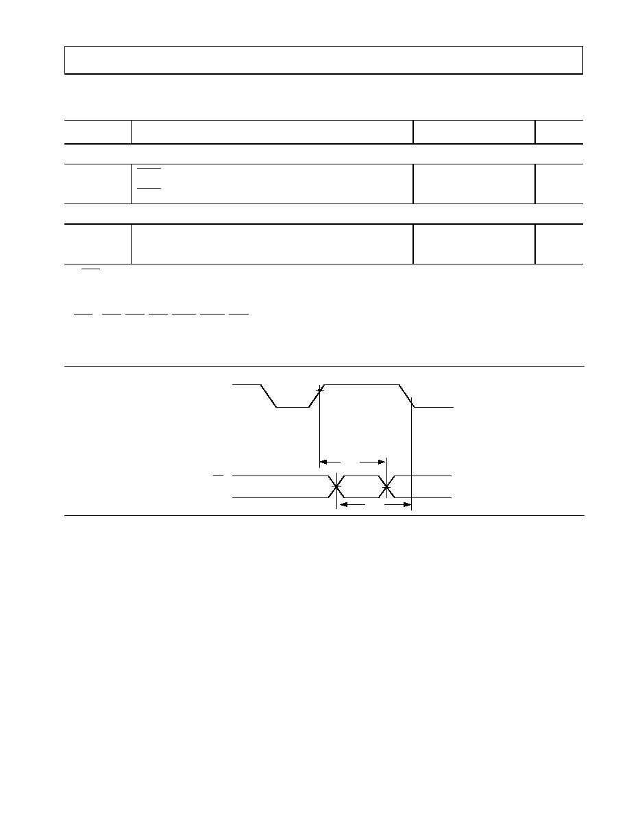
Figure 20. Interrupts and Flags
t
IF H
t
IF S
CLKOUT
IR Q
x
FI
PFx

28
6/2001 REV. PrB
For current information contact Analog Devices at (800) ANALOGD
ADSP-21mod980N
PRELIMINARY TECHNICAL DATA
Serial Ports
Table 11. Serial Ports
Parameter
Description
Min.
Max
Unit
Timing Requirements:
t
SCK
SCLK Period
30
ns
t
SCS
DR/TFS/RFS Setup before SCLK Low
4
ns
t
SCH
DR/TFS/RFS Hold after SCLK Low
7
ns
t
SCP
SCLKIN Width
12
ns
Switching Characteristics:
t
CC
CLKOUT High to SCLKOUT
0.25t
CK
0.25t
CK
+ 6
ns
t
SCDE
SCLK High to DT Enable
0
ns
t
SCDV
SCLK High to DT Valid
12
ns
t
RH
TFS/RFSOUT Hold after SCLK High
0
ns
t
RD
TFS/RFSOUT Delay from SCLK High
12
ns
t
SCDH
DT Hold after SCLK High
0
ns
t
TDE
TFS (Alt) to DT Enable
0
ns
t
TDV
TFS (Alt) to DT Valid
12
ns
t
SCDD
SCLK High to DT Disable
12
ns
t
RDV
RFS (Multichannel, Frame Delay Zero to DT Valid
12
ns
29
REV. PrB
6/2001
For current information contact Analog Devices at (800) ANALOGD
ADSP-21mod980N
PRELIMINARY TECHNICAL DATA
Figure 21. Serial Ports
CL K O U T
S CL K
T F S
O U T
RF S O UT
DT
A L T E R N A T E
FR A M E M O D E
t
C C
t
C C
t
S C S
t
S C H
t
R H
t
S C D E
t
S C D H
t
S C D D
t
T D E
t
R D V
M U L T IC H A N N E L
M O D E ,
F R A M E D E L A Y 0
(M F D = 0 )
DR
TF S
IN
RFS
IN
RFS
O UT
TFS
OU T
t
T D V
t
S C D V
t
R D
t
S C P
t
S C K
t
S C P
T F SIN
RF S IN
A L T E R N A T E
FR A M E M O D E
t
R D V
M U L T IC H A N N E L
M O D E ,
F R A M E D E L A Y 0
(M F D = 0 )
t
T D E
t
T D V
30
6/2001 REV. PrB
For current information contact Analog Devices at (800) ANALOGD
ADSP-21mod980N
PRELIMINARY TECHNICAL DATA
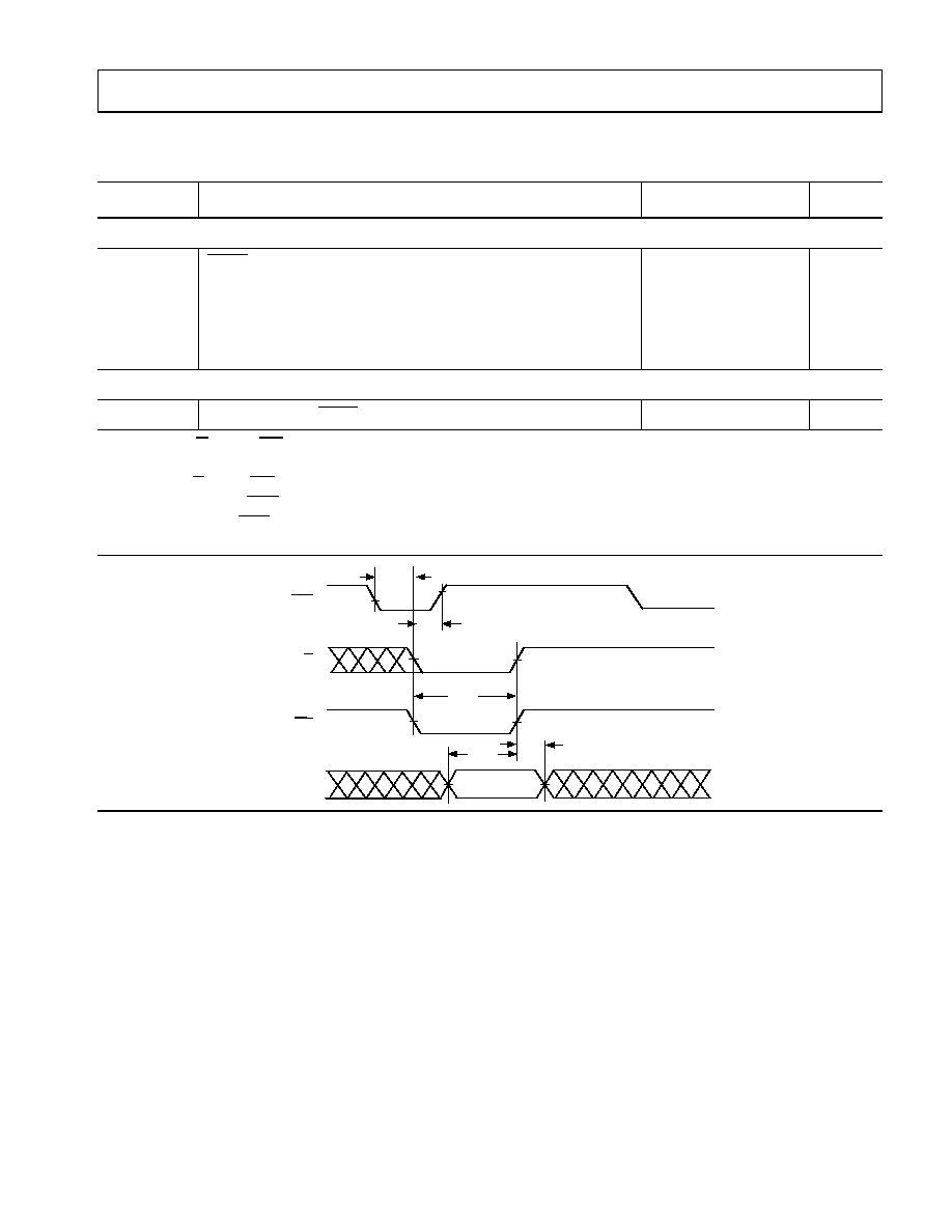
IDMA Address Latch
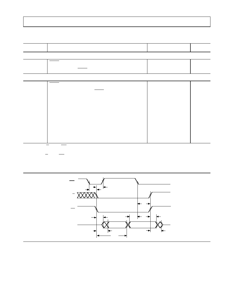
Table 12. IDMA Address Latch
Parameter
Description
Min.
Max
Unit
Timing Requirements:
t
IALP
Duration of Address Latch
1, 2, 3
10
ns
t
IASU
IAD[15:0] Address Setup before Address Latch End
2, 3
5
ns
t
IAH
IAD[15:0] Address Hold after Address Latch End
2, 3
3
ns
t
IKA
IACK Low before Start of Address Latch
2, 3,
4
0
ns
t
IALS
Start of Write or Read after Address Latch End
2,
3, 4
3
ns
t
IALD
Address Latch Start after Address Latch End
1,
2, 3
2
ns
1
Start of Address Latch = IS Low and IAL High.
2
End of Address Latch = IS High or IAL Low.
3
For IDMA, please refer to the ADSP-2100 Family User's Manual.
4
Start of Write or Read = IS Low and IWR Low or IRD Low.
Figure 22. IDMA Address Latch
IA D 15-0
t
IK A
IRD
IWR
OR
IA C K
IA L
IS
t
IA L P
t
IA L D
t
IA L S
t
IA S U
t
IA S U
t
IA H
t
IA H
t
IA L P
31
REV. PrB
6/2001
For current information contact Analog Devices at (800) ANALOGD
ADSP-21mod980N
PRELIMINARY TECHNICAL DATA
IDMA Write, Short Write Cycle
Table 13. IDMA Write, Short Write Cycle
Parameter
Description
Min.
Max
Unit
Timing Requirements:
t
IKW
IACK Low before Start of Write
1, 2
0
ns
t
IWP
Duration of Write
1, 2,
3
10
ns
t
IDSU
IAD[15:0] Data Setup before End of Write
2, 3, 4, 5
3
ns
t
IDH
IAD[15:0] Data Hold after End of Write
2, 3, 4, 5
2
ns
Switching Characteristics:
t
IKHW
Start of Write to IACK High
10
ns
1
Start of Write = IS Low and IWR Low.
2
For IDMA, please refer to the ADSP-2100 Family User's Manual.
3
End of Write = IS High or IWR High.
4
If Write Pulse ends before IACK Low, use specifications t
IDSU
, t
IDH
.
5
If Write Pulse ends after IACK Low, use specifications t
IKSU
, t
IKH
.
Figure 23. IDMA Write, Short Write Cycle
IA D 15-0
DA T A
t
IKHW
t
IKW
t
ID SU
IA C K
t
IW P
t
IDH
IS
IW R
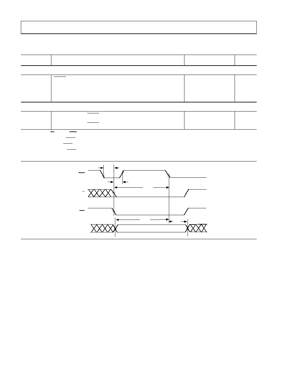
32
6/2001 REV. PrB
For current information contact Analog Devices at (800) ANALOGD
ADSP-21mod980N
PRELIMINARY TECHNICAL DATA
IDMA Write, Long Write Cycle
Table 14. IDMA Write, Long Write Cycle
Parameter
Description
Min.
Max
Unit
Timing Requirements
t
IKW
IACK Low before Start of Write
1
0
ns
t
IKSU
IAD[15:0] Data Setup before End of Write
2, 3, 4
0.5t
CK
+ 5
ns
t
IKH
IAD[15:0] Data Hold after End of Write
2, 3, 4
0
ns
Switching Characteristics:
t
IKLW
Start of Write to IACK Low
4
1.5t
CK
ns
t
IKHW
Start of Write to IACK High
10
ns
1
Start of Write = IS Low and IWR Low.
2
If Write Pulse ends before IACK Low, use specifications t
IDSU
, t
IDH
.
3
If Write Pulse ends after IACK Low, use specifications t
IKSU
, t
IKH
.
4
This is the earliest time for IACK Low from Start of Write. For IDMA Write cycle relationships, please refer to the ADSP-2100 Family User's Manual.
Figure 24. IDMA Write, Long Write Cycle
IAD 15-0
DA T A
t
IKHW
t
IK W
IAC K
IS
IW R
t
IKLW
t
IKH
t
IKSU
33
REV. PrB
6/2001
For current information contact Analog Devices at (800) ANALOGD
ADSP-21mod980N
PRELIMINARY TECHNICAL DATA
IDMA Read, Long Read Cycle
Table 15. IDMA Read, Long Read Cycle
Parameter
Description
Min.
Max
Unit
Timing Requirements:
t
IKR
IACK Low before Start of Read
1, 2
0
ns
t
IRK
End of Read after IACK Low
2,
3
2
ns
Switching Characteristics:
t
IKHR
IACK High after Start of Read
1, 2
10
ns
t
IKDS
IAD[15:0 Data Setup before IACK Low
2
0.5t
CK
- 2
ns
t
IKDH
IAD[15:0] Data Hold after End of Read
2, 3
0
ns
t
IKDD
IAD[15:0] Data Disabled after End of Read
2, 3
10
ns
t
IRDE
IAD[15:0] Previous Data Enabled after Start of Read
2
0
ns
t
IRDV
IAD[15:0] Previous Data Valid after Start of Read
2
10
ns
t
IRDH
1
IAD[15:0] Previous Data Hold after Start of Read
(DM/PM1)
2, 4
2t
CK
- 5
ns
t
IRDH
2
IAD[15:0] Previous Data Hold after Start of Read (PM2)
2, 5
t
CK
- 5
ns
1
Start of Read = IS Low and IRD Low.
2
For IDMA, please refer to the ADSP-2100 Family User's Manual.
3
End of Read = IS High or IRD High.
4
DM read or first half of PM read.
5
Second half of PM read.
Figure 25. IDMA Read, Long Read Cycle
t
IR K
t
IK R
P RE V IO US
DA T A
RE A D
DA T A
t
IK H R
t
IK D S
t
IR D V
t
IR D H
t
IK D D
t
IR D E
t
IK D H
IA D 15-0
IA C K
IS
IR D
34
6/2001 REV. PrB
For current information contact Analog Devices at (800) ANALOGD
ADSP-21mod980N
PRELIMINARY TECHNICAL DATA
IDMA Read, Short Read Cycle
Table 16. IDMA Read, Short Read Cycle
1
Parameter
Description
Min.
Max
Unit
Timing Requirements:
t
IKR
IACK Low before Start of Read
2
0
ns
t
IRP
Duration of Read
10
ns
Switching Characteristics:
t
IKHR
IACK High after Start of Read
2, 3
10
ns
t
IKDH
IAD[15:0] Data Hold after End of Read
3, 4
0
ns
t
IKDD
IAD[15:0] Data Disabled after End of Read
3, 4
10
ns
t
IRDE
IAD[15:0] Previous Data Enabled after Start of Read
3
0
ns
t
IRDV
IAD[15:0] Previous Data Valid after Start of Read
3
10
ns
t
IRDH
1
IAD[15:0] Previous Data Hold after Start of Read
(DM/PM1)
3,5
2t
CK
- 5
ns
t
IRDH
2
IAD[15:0] Previous Data Hold after Start of Read (PM2)
3, 6
t
CK
- 5
ns
1
Timing applies to ADSP-21mod980N when Short Read Only mode is disabled. See
Table on page 35
.
2
Start of Read = IS Low and IRD Low.
3
For IDMA, please refer to the ADSP-2100 Family User's Manual.
4
End of Read = IS High or IRD High.
5
DM read or first half of PM read.
6
Second half of PM read.
Figure 26. IDMA Read, Short Read Cycle
IACK
IS
IR D
tIKR
tIKHR
tIRDE
tIRDV
Previous Data
New Read Data
IAD[15:0]
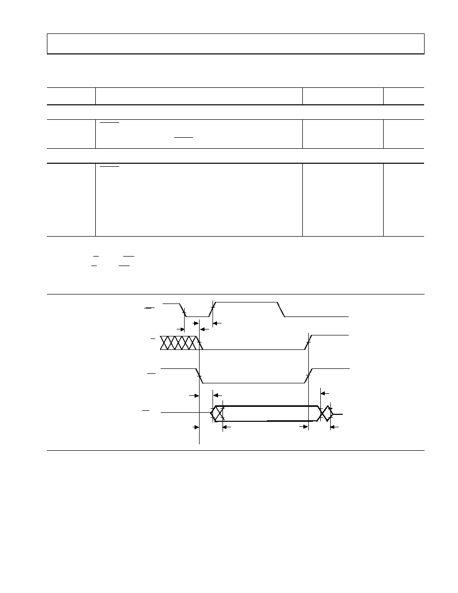
35
REV. PrB
6/2001
For current information contact Analog Devices at (800) ANALOGD
ADSP-21mod980N
PRELIMINARY TECHNICAL DATA
IDMA Read - Short Read Cycle in Short Read Only Mode
Table 17. IDMA Read - Short Read Cycle in Short Read Only Mode
1
1
Short Read Only is enabled by setting Bit 14 of the IDMA Overlay Register to 1 (0x3FE7). Short Read Only can be enabled by the processor core writing
to the register or by an external host writing to the register. Disabled by default.
Parameter
Description
Min.
Max
Unit
Timing Requirements:
t
IKR
IACK Low before Start of Read
2, 4
2
Start of Read = IS Low and IRD Low. Previous data remains until end of read.
0
ns
t
IRP
Duration of Read after IACK Low
3, 4
3
End of Read = IS High or IRD High.
10
ns
Switching Characteristics:
t
IKHR
IACK High after Start of Read
2, 4
4
For IDMA, please refer to the ADSP-2100 Family User's Manual.
10
ns
t
IKDH
IAD[15:0] Previous Data Hold after End of Read
3, 4
0
ns
t
IKDD
IAD[15:0] Previous Data Disabled after End of Read
3, 4
10
ns
t
IRDE
IAD[15:0] Previous Data Enabled after Start of Read
4
0
ns
t
IRDV
IAD[15:0] Previous Data Valid after Start of Read
4
10
ns
Figure 27. IDMA Read, Short Read Only Mode
IACK
IS
IR D
tIRDE
tRDV
tIKR
tIKHR
tIKDH
tIKDD
Previous Data
IAD[15:0]
36
6/2001 REV. PrB
For current information contact Analog Devices at (800) ANALOGD
ADSP-21mod980N
PRELIMINARY TECHNICAL DATA
352-BALL PBGA
PACKAGE PINOUT
A physical layout of all sig-
nals is shown in the
following tables.
Figure on
page 40
shows the signals
on the left side of the device
when viewed from the top.
Figure on page 41
shows
the signals on the right side
of the device when viewed
from the top. The pin num-
ber for each signal is listed
in
Table on page 36
.
Table 18. Pinout by
Signal Name
Signal Name
Pin
A0
A2
BG_1
F3
BG_2
D14
BG_3
F25
BG_4
AC5
BG_5
R25
BG_6
R4
BG_7
AD15
BG_8
AD25
BR_1
G4
BR_2
B13
BR_3
G25
BR_4
AC9
BR_5
N24
BR_6
U4
BR_7
AE15
BR_8
AE26
CLKIN
E3
CLKOUT_1
G1
CLKOUT_2
A10
CLKOUT_3
C20
CLKOUT_4
AC1
CLKOUT_5
L24
CLKOUT_6
P4
CLKOUT_7
AD10
CLKOUT_8
AF15
D08
F23
D09
E25
D10
E24
D11
D26
D12
D25
D13
D24
D14
C26
D15
C25
D16
B26
D17
B24
D18
A25
D19
B23
D20
C23
D21
A24
D22
A23
D23
A22
DR0A
E1
DR0B
AF22
DR1
AE7
DT0A
P2
DT0B
AF20
DT1_1
P3
DT1_2
A12
DT1_3
D21
Table 18. Pinout by
Signal Name (Continued)
Signal Name
Pin
DT1_4
AF2
DT1_5
T25
DT1_6
U3
DT1_7
AD13
DT1_8
AE20
EBG
F26
EBR
G26
ECLK
J23
EE_1
M4
EE_2
C13
EE_3
G23
EE_4
AE9
EE_5
T26
EE_6
Y2
EE_7
AC13
EE_8
AE22
EINT
J26
ELIN
J25
ELOUT
J24
EMS
E23
ERESET
E26
GND
D19
GND
D20
GND
D23
GND
F1
GND
F2
GND
F4
GND
G2
GND
G3
GND
H1
Table 18. Pinout by
Signal Name (Continued)
Signal Name
Pin
GND
H2
GND
H3
GND
H4
GND
H23
GND
H24
GND
H25
GND
H26
GND
N1
GND
N2
GND
N3
GND
N4
GND
R23
GND
R24
GND
T3
GND
T24
GND
U1
GND
U2
GND
U23
GND
U24
GND
U25
GND
U26
GND
W1
GND
W2
GND
W3
GND
W4
GND
AF1
GND
AF4
GND
AF8
GND
AF10
GND
AF12
Table 18. Pinout by
Signal Name (Continued)
Signal Name
Pin
37
REV. PrB
6/2001
For current information contact Analog Devices at (800) ANALOGD
ADSP-21mod980N
PRELIMINARY TECHNICAL DATA
GND
AF16
GND
AF17
GND
AF21
GND
AF23
GND
AF26
GND
B2
GND
B5
GND
B11
GND
B12
GND
B16
GND
B19
GND
B21
GND
B25
GND
C3
GND
C5
GND
C11
GND
C16
GND
C19
GND
C21
GND
C24
GND
D4
GND
D5
GND
D11
GND
D16
GND
AC12
GND
AC17
GND
AC21
GND
AC23
GND
AD2
GND
AD3
Table 18. Pinout by
Signal Name (Continued)
Signal Name
Pin
GND
AD4
GND
AD5
GND
AD7
GND
AD8
GND
AD11
GND
AD12
GND
AD16
GND
AD17
GND
AD21
GND
AD22
GND
AD23
GND
AD24
GND
AE1
GND
AE2
GND
AE4
GND
AE8
GND
AE10
GND
AE12
GND
AE16
GND
AE17
GND
AE21
GND
AE23
GND
AE25
GND
A1
GND
A5
GND
A11
GND
A16
GND
A19
GND
A20
GND
A21
Table 18. Pinout by
Signal Name (Continued)
Signal Name
Pin
GND
A26
GND
AA23
GND
AA24
GND
AA25
GND
AA26
GND
AC4
GND
AC6
GND
AC8
GND
AC10
GND
W23
IACK_A
T4
IACK_B
AC26
IAD0_A
B4
IAD0_B
V26
IAD1_A
B1
IAD1_B
V23
IAD10_A
AA2
IAD10_B
L26
IAD11_A
V3
IAD11_B
L23
IAD12_A
AA4
IAD12_B
M25
IAD13_A
E2
IAD13_B
AD26
IAD14_A
D1
IAD14_B
AC24
IAD15_A
E4
IAD15_B
AC25
IAD2_A
C2
IAD2_B
V24
Table 18. Pinout by
Signal Name (Continued)
Signal Name
Pin
IAD3_A
D3
IAD3_B
W24
IAD4_A
C1
IAD4_B
W25
IAD5_A
D2
IAD5_B
W26
IAD6_A
V4
IAD6_B
M26
IAD7_A
Y4
IAD7_B
N26
IAD8_A
AD6
IAD8_B
M23
IAD9_A
Y3
IAD9_B
M24
IAL_A
C8
IAL_B
Y25
IRD_A
C4
IRD_B
Y24
IS_1
D6
IS_2
A14
IS_3
F24
IS_4
AA3
IS_5
V25
IS_6
AC7
IS_7
AC16
IS_8
Y26
IWR_A
D8
IWR_B
Y23
PF0
A6
PF1
B6
Table 18. Pinout by
Signal Name (Continued)
Signal Name
Pin
38
6/2001 REV. PrB
For current information contact Analog Devices at (800) ANALOGD
ADSP-21mod980N
PRELIMINARY TECHNICAL DATA
PF2
C6
PF4_1
M1
PF4_2
C10
PF4_3
D18
PF4_4
AC2
PF4_5
L25
PF4_6
T1
PF4_7
AF7
PF4_8
AD18
PF5_1
M2
PF5_2
D10
PF5_3
C18
PF5_4
AC3
PF5_5
G24
PF5_6
V1
PF5_7
AE11
PF5-8
AE18
PF6_1
M3
PF6_2
B10
PF6_3
B18
PF6_4
AD1
PF6_5
R26
PF6_6
T2
PF6_7
AD9
PF6_8
AC18
PF7_1
J4
PF7_2
D12
PF7_3
A18
PF7_4
AE3
PF7_5
N25
Table 18. Pinout by
Signal Name (Continued)
Signal Name
Pin
PF7_6
V2
PF7_7
AF9
PF7_8
AF18
RESET_1
J1
RESET_2
D13
RESET_3
C22
RESET_4
AF6
RESET_5
T23
RESET_6
AA1
RESET_7
AC11
RESET_8
AC22
RFS0A
J3
RFS0B
AD20
RFS1
AE6
SCLK0A
P1
SCLK0B
AE24
SCLK1
AF5
TFS0_1
J2
TFS0_2
C12
TFS0_3
B20
TFS0_4
AE5
TFS0_5
N23
TFS0_6
Y1
TFS0_7
AF11
TFS0_8
AC20
TFS1
AF3
VDDEXT
B22
VDDEXT
C7
VDDEXT
C9
VDDEXT
C14
Table 18. Pinout by
Signal Name (Continued)
Signal Name
Pin
VDDEXT
C15
VDDEXT
C17
VDDEXT
D7
VDDEXT
D9
VDDEXT
D15
VDDEXT
D17
VDDEXT
D22
VDDEXT
K1
VDDEXT
K2
VDDEXT
K3
VDDEXT
K4
VDDEXT
K23
VDDEXT
K24
VDDEXT
K25
VDDEXT
K26
VDDEXT
L1
VDDEXT
L2
VDDEXT
L3
VDDEXT
L4
VDDEXT
A7
VDDEXT
A8
VDDEXT
A9
VDDEXT
A13
VDDEXT
A15
VDDEXT
A17
VDDEXT
AC14
VDDEXT
AC15
VDDEXT
AC19
VDDEXT
AD14
VDDEXT
AD19
Table 18. Pinout by
Signal Name (Continued)
Signal Name
Pin
VDDEXT
AE14
VDDEXT
AE19
VDDEXT
AF14
VDDEXT
AF19
VDDEXT
B7
VDDEXT
B8
VDDEXT
B9
VDDEXT
B14
VDDEXT
B15
VDDEXT
B17
VDDINT
A3
VDDINT
A4
VDDINT
AB1
VDDINT
AB2
VDDINT
AB3
VDDINT
AB4
VDDINT
AB23
VDDINT
AB24
VDDINT
AB25
VDDINT
AB26
VDDINT
AE13
VDDINT
AF13
VDDINT
AF24
VDDINT
AF25
VDDINT
B3
VDDINT
P23
VDDINT
P24
VDDINT
P25
VDDINT
P26
Table 18. Pinout by
Signal Name (Continued)
Signal Name
Pin

39
REV. PrB
6/2001
For current information contact Analog Devices at (800) ANALOGD
ADSP-21mod980N
PRELIMINARY TECHNICAL DATA
VDDINT
R1
VDDINT
R2
VDDINT
R3
Table 18. Pinout by
Signal Name (Continued)
Signal Name
Pin

40
6/2001 REV. PrB
For current information contact Analog Devices at (800) ANALOGD
ADSP-21mod980N
PRELIMINARY TECHNICAL DATA
Signals by Pin Location--Top View, Left to Right
1
2
3
4
5
6
7
8
9
10
11
12
13
A
GND
A0
VDDINT
VDDINT
GND
PF0
VDDEXT
VDDEXT
VDDEXT
CLKOUT_2
GND
DT1_2
VDDEXT
B
IAD1_A
GND
VDDINT
IAD0_A
GND
PF1
VDDEXT
VDDEXT
VDDEXT
PF6_2
GND
GND
BR_2
C
IAD4_A
IAD2_A
GND
IRD_A
GND
PF2
VDDEXT
IAL_A
VDDEXT
PF4_2
GND
TFS0_2
EE_2
D
IAD14_A
IAD6_A
IAD3_A
GND
GND
IS_1
VDDEXT
IWR_A
VDDEXT
PF5_2
GND
PF7_2
RESET_2
E
DR0A
IAD13_A
CLKIN
IAD15_A
F
GND
GND
BG_1
GND
G
CLKOUT_1
GND
GND
BR_1
H
GND
GND
GND
GND
J
RESET_1
TFS0_1
RFS0A
PF7_1
K
VDDEXT
VDDEXT
VDDEXT
VDDEXT
L
VDDEXT
VDDEXT
VDDEXT
VDDEXT
M
PF4_1
PF5_1
PF6_1
EE_1
N
GND
GND
GND
GND
P
SCLK0A
DT0A
DT1_1
CLKOUT_6
R
VDDINT
VDDINT
VDDINT
BG_6
T
PF4_6
PF6_6
GND
IACK_A
U
GND
GND
DT1_6
BR_6
V
PF5_6
PF7_6
IAD11_A
IAD6_A
W
GND
GND
GND
GND
Y
TFS0_6
EE_6
IAD9_A
IAD7_A
AA
RESET_6
IAD10_A
IS_4
IAD12_A
AB
VDDINT
VDDINT
VDDINT
VDDINT
AC
CLKOUT_4
PF4_4
PF5_4
GND
BG_4
GND
IS_6
GND
BR_4
GND
RESET_7
GND
EE_7
AD
PF6_4
GND
GND
GND
GND
IAD8_A
GND
GND
PF6_7
CLKOUT_7
GND
GND
DT1_7
AE
GND
GND
PF7_4
GND
TFS0_4
RFS1
DR1
GND
EE_4
GND
PF5_7
GND
VDDINT
AF
GND
DT1_4
TFS1
GND
SCLK1
RESET_4
PF4_7
GND
PF7_7
GND
TFS0_7
GND
VDDINT
1
2
3
4
5
6
7
8
9
10
11
12
13

41
REV. PrB
6/2001
For current information contact Analog Devices at (800) ANALOGD
ADSP-21mod980N
PRELIMINARY TECHNICAL DATA
OUTLINE DIMENSIONS 352 PLASTIC BALL GRID ARRAY
Signals by Pin Location--Top View, Left to Right (Continued)
14
15
16
17
18
19
20
21
22
23
24
25
26
IS_2
VDDEXT
GND
VDDEXT
PF7_3
GND
GND
GND
D23
D22
D21
D18
GND
A
VDDEXT
VDDEXT
GND
VDDEXT
PF6_3
GND
TRS0_3
GND
VDDEXT
D19
D17
GND
D16
B
VDDEXT
VDDEXT
GND
VDDEXT
PF5_3
GND
CLKOUT_3
GND
RESET_3
D20
GND
D15
D14
C
BG_2
VDDEXT
GND
VDDEXT
PF4_3
GND
GND
DT1_3
VDDEXT
GND
D13
D12
D11
D
EMS
D10
D09
ERESET
E
D08
IS_3
BG_3
EBG
F
EE_3
PF5_5
BR_3
EBR
G
GND
GND
GND
GND
H
ECLK
ELOUT
ELIN
EINT
J
VDDEXT
VDDEXT
VDDEXT
VDDEXT
K
IAD11_B
CLKOUT_5
PF4_5
IAD10_B
L
IAD8_B
IAD9_B
IAD12_B
IAD6_B
M
TFS0_5
BR_5
PF7_5
IAD7_B
N
VDDINT
VDDINT
VDDINT
VDDINT
P
GND
GND
BG_5
PF6_5
R
RESET_5
GND
DT1_5
EE_5
T
GND
GND
GND
GND
U
IAD1_B
IAD2_B
IS_5
IAD0_B
V
GND
IAD3_B
IAD4_B
IAD5_B
W
IWR_B
IRD_B
IAL_B
IS_8
Y
GND
GND
GND
GND
AA
VDDINT
VDDINT
VDDINT
VDDINT
AB
VDDEXT
VDDEXT
IS_7
GND
PF6_8
VDDEXT
TFS0_8
GND
RESET_8
GND
IAD14_B
IAD15_B
IACK_B
AC
VDDEXT
BG_7
GND
GND
PF4_8
VDDEXT
RFS0B
GND
GND
GND
GND
BG_8
IAD13_B
AD
VDDEXT
BR_7
GND
GND
PF5_8
VDDEXT
DT1_8
GND
EE_8
GND
SCLK0B
GND
BR_8
AE
VDDEXT
CLKOUT_8
GND
GND
PF7_8
VDDEXT
DT0B
GND
DR0B
GND
VDDINT
VDDINT
GND
AF
14
15
16
17
18
19
20
21
22
23
24
25
26
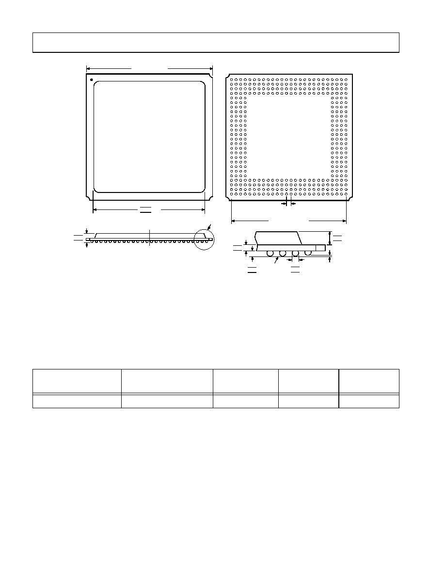
42
6/2001 REV. PrB
For current information contact Analog Devices at (800) ANALOGD
ADSP-21mod980N
PRELIMINARY TECHNICAL DATA
ORDERING GUIDE
A complete modem requires the device listed in
Table
19
plus a software solution as described in
M
ODEM
S
OFTWARE
on page 2.
Figure 28. 352-Lead metric Plastic Ball Grid Array (PBGA) (B-352)
DE T A IL A
2.62
2.37
2.12
BO T T O M V IE W
A
B
C
D
E
F
G
H
J
K
L
M
N
P
R
T
U
V
W
Y
A A
A B
A C
A D
A E
A F
25
23
21
19
17
15
13
11
9
7
5
3
1
26
24
22
20
18
16
14
12
10
8
6
4
2
1.27 B S C S Q
BA L L P ITC H
31.75 BS C S Q
35.00 BS C S Q
T O P V IE W
BA L L A1
IN DIC AT O R
30.70
30.00 S Q
29.50
1.22
1.17
1.12
S E AT IN G
P L AN E
0.20 M AX
D ET A IL A
0.90
0.75
0.60
BA L L DIA M E T E R
0.70
0.60
0.50
0.70
0.60
0.50
NO T E S :
1. T HE AC T UA L P O S IT IO N O F T HE B AL L G R ID IS W IT HIN 0.30
O F T HE IDE A L P O S IT IO N R E L A TIV E T O TH E P AC KAG E E DG E S .
2. T HE AC T UA L P O S IT IO N O F E A CH BA L L IS W IT HIN 0.15 O F ITS
ID E AL PO S ITIO N RE L AT IV E T O THE B AL L G RID .
3. CE N T E R F IG U RE S A RE N O M INA L UN LE S S O T HE RW IS E NO T E D.
Table 19. Ordering Guide
Part Number
Ambient Temperature
Range
Instruction Rate
Package
Description
Package Option
ADSP-21mod980N-000
0ºC to +70ºC
80 MHz
352-Ball PBGA
B-352
Document Outline
- Specifications
- ELECTRICAL CHARACTERISTICS
- Pinout
- Package drawings
- ORDERING GUIDE
- Features
- Product Description
- ABSOLUTE MAXIMUM RATINGS
- Functional Block Diagram
- MODEM SOFTWARE
- DEVELOPMENT SYSTEM
- ADDITIONAL INFORMATION
- ARCHITECTURE OVERVIEW
- SERIAL PORTS
- PIN DESCRIPTIONS
- MEMORY INTERFACE PINS
- INTERRUPTS
- LOW POWER OPERATION
- POWER DOWN
- SYSTEM CONFIGURATION
- IDLE
- SLOW IDLE
- CLOCK SIGNALS
- RESET
- MEMORY ARCHITECTURE
- MEMORY MAPPED REGISTERS (NEW TO THE ADSP-21MOD980N)
- SLAVE MODE
- IDMA PORT BOOTING
- FLAG I/O PINS
- DESIGNING AN EZ-ICE-COMPATIBLE SYSTEM
- TARGET MEMOR Y INTERF ACE
- TARGET SYSTEM INTERFACE SIGNALS
- TARGET BOARD CONNECTOR FOR EZ-ICE PROBE
- DIAGRAMS
- MOD980N MultiPort Internet Gateway Processor Block Diagram
- ADSP-21mod980N Functional Block Diagram
- Multichannel Modem Configuration
- Program Memory Map
- Data Memory Map
- Waitstate Control Register
- Programmable Flag1 & Composite Select Control Register
- System Control Register
- IDMA Control/OVLAY Registers
- Direct Memory Access - PM and DM Memory Maps
- Selecting a Modem Processor in the ADSP-21mod980N
- Target Board Connector for EZ-ICE
- Voltage Reference Levels for AC Measurements (Except Output Enable/Disable)
- Equivalent Loading for AC Measurements (Including All Fixtures)
- Untitled
- Clock and Reset Signals
- Interrupts and Flags
- Serial Ports
- IDMA Address Latch
- IDMA Write, Short Write Cycle
- IDMA Write, Long Write Cycle
- IDMA Read, Long Read Cycle
- IDMA Read, Short Read Cycle
- IDMA Read, Short Read Only Mode
- 352-Lead metric Plastic Ball Grid Array (PBGA) (B-352)