Äîêóìåíòàöèÿ è îïèñàíèÿ www.docs.chipfind.ru
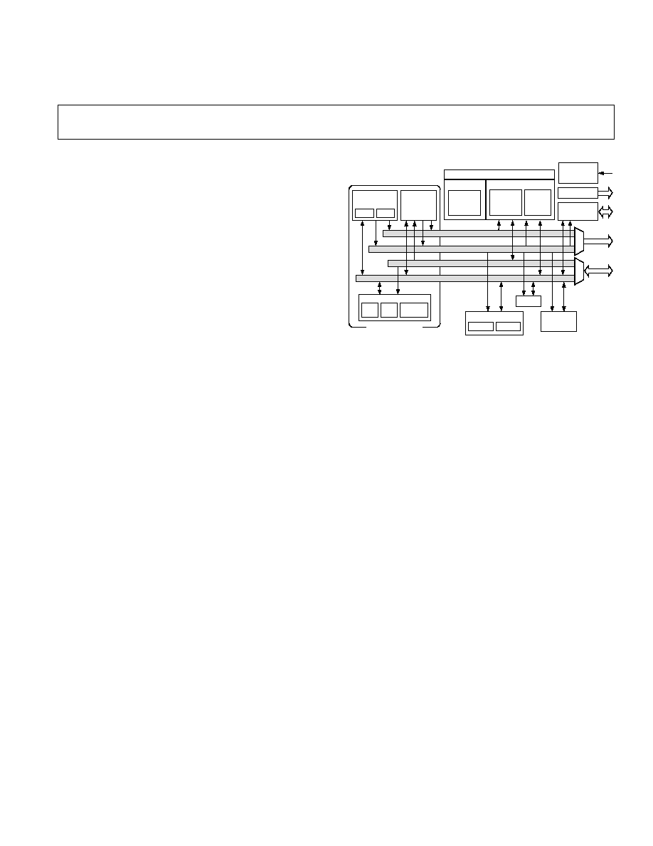
FUNCTIONAL BLOCK DIAGRAM
MEMORY
PROGRAM
MEMORY
4K x 24
(ROM)
ADSP-21msp59
PROGRAM
MEMORY
2K x 24
DATA
MEMORY
2K x 16
ADSP-21msp58/59
ALU
MAC
SHIFTER
ARITHMETIC UNITS
EXTERNAL
ADDRESS
BUS
EXTERNAL
DATA
BUS
HOST
INTERFACE
PORT
SERIAL PORTS
SPORT 0
SPORT 1
TIMER
DAG 1
DAG 2
DATA
ADDRESS
GENERATORS
PROGRAM
SEQUENCER
POWERDOWN
CONTROL
LOGIC
FLAG
DATA MEMORY DATA
DATA MEMORY ADDRESS
PROGRAM MEMORY ADDRESS
ANALOG
INTERFACE
ADSP-2100 BASE
ARCHITECTURE
PROGRAM MEMORY DATA
REV. 0
Information furnished by Analog Devices is believed to be accurate and
reliable. However, no responsibility is assumed by Analog Devices for its
use, nor for any infringements of patents or other rights of third parties
which may result from its use. No license is granted by implication or
otherwise under any patent or patent rights of Analog Devices.
a
DSP Microcomputers
ADSP-21msp58/59
© Analog Devices, Inc., 1995
One Technology Way, P.O. Box 9106, Norwood. MA 02062-9106, U.S.A.
Tel: 617/329-4700
Fax: 617/326-8703
FEATURES
38 ns Instruction Cycle Time (26 MIPS) from 13.00 MHz
Crystal
ADSP-2100 Family Code and Function Compatible with
New Instruction Set Enhanced for Bit Manipulation
Instructions, Multiplication Instructions, Biased
Rounding, and Global Interrupt Masking
2K 24 Words of On-Chip Program Memory RAM
2K 16 Words of On-Chip Data Memory RAM
4K 24 Words of On-Chip Program Memory ROM
(ADSP-21msp59 Only)
8-Bit Parallel Host Interface Port
Analog Interface Provides:
16-Bit Sigma-Delta ADC and DAC
Programmable Gain Stages
On-Chip Anti-Aliasing & Anti-Imaging Filters
8 kHz Sampling Frequency
65 dB ADC, SNR and THD
72 dB DAC, SNR and THD
425 mW Typical Power Dissipation @ 5.0 V @ 38 ns
<1 mW Powerdown Mode with 100 Cycle Recovery
Dual Purpose Program Memory for Both Instruction
and Data Storage
Independent ALU, Multiplier/Accumulator, and Barrel
Shifter Computational Units
Two Independent Data Address Generators
Powerful Program Sequencer Provides:
Zero Overhead Looping
Conditional Instruction Execution
Two Double-Buffered Serial Ports with Companding
Hardware, One Serial Port (SPORT0) has Automatic
Data Buffering
Programmable 16-Bit Interval Timer with Prescaler
Programmable Wait State Generation
Automatic Booting of Internal Program Memory from
Byte-Wide External Memory, e.g., EPROM, or
Through Host Interface Port
Stand-Alone ROM Execution (ADSP-21msp59 Only)
Single-Cycle Instruction Execution
Single-Cycle Context Switch
Multifunction Instructions
Three Edge- or Level-Sensitive External Interrupts
Low Power Dissipation in Standby Mode
100-Lead TQFP
GENERAL DESCRIPTION
The ADSP-21msp58 and ADSP-21msp59 Mixed-Signal Pro-
cessors (MSProcessor
®
DSPs) are fully integrated, single-chip
DSPs complete with a high performance analog front end. The
ADSP-21msp58/59 Family is optimized for voice band applica-
tions such as Speech Compression, Speech Processing, Speech
Recognition, Text-to Speech, and Speech-to-Text conversion.
The ADSP-21msp58/59 combines the ADSP-2100 base archi-
tecture (three computation units, data address generators, and
program sequencer) with two serial ports, a host interface port,
an analog front end, a programmable timer, extensive interrupt
capability, and on-chip program and data memory.
The ADSP-21msp58 provides 2K words (24-bit) of program
RAM and 2K words (16-bit) of data memory. The ADSP-
21msp59 provides an additional 4K words (24-bit) of program
ROM. The ADSP-21msp58/59 integrates a high performance
analog codec based on a single chip, voice band codec, the
AD28msp02. Powerdown circuitry is also provided to meet the
low power needs of battery operated portable equipment. The
ADSP-21msp58/59 is available in a 100-pin TQFP package
(thin quad flat package).
In addition, the ADSP-21msp58/59 supports new instructions,
which include bit manipulationsbit set, bit clear, bit toggle,
bit testnew ALU constants, new multiplication instruction
(x squared), biased rounding, and global interrupt masking.
MSProcessor is a registered trademark of Analog Devices, Inc.
REV. 0
2
ADSP-21msp58/59
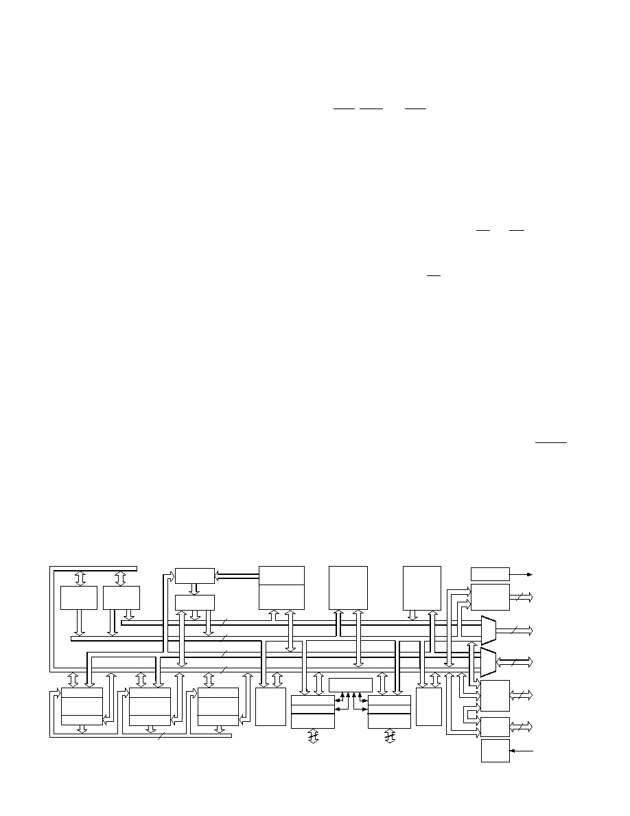
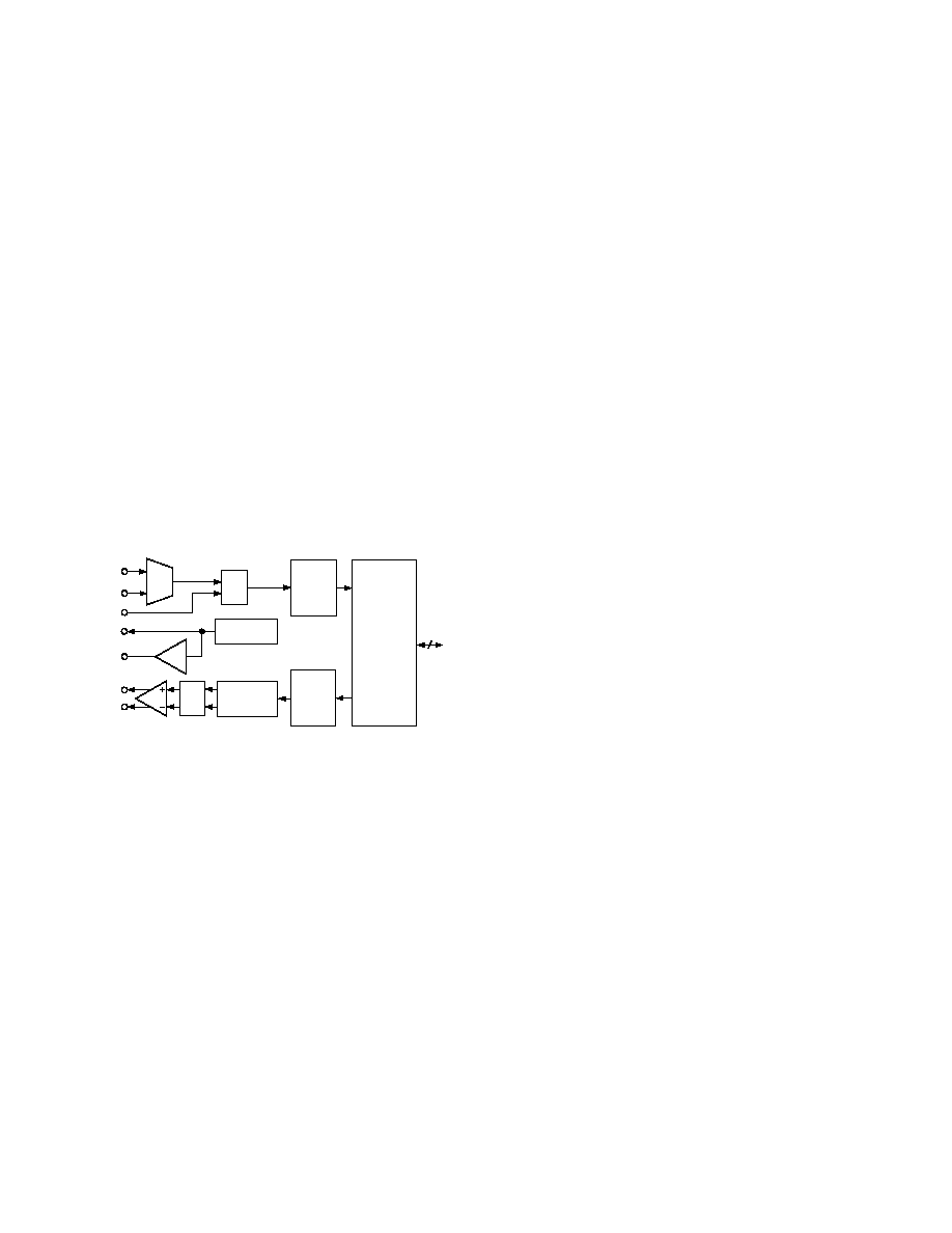
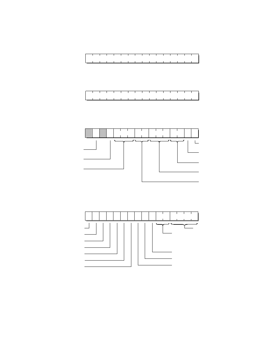
DIGITAL ARCHITECTURE OVERVIEW
Figure 1 is an overall block diagram of the ADSP-21msp58/59.
The processors contain three independent computational units:
the ALU, the multiplier/accumulator (MAC), and the shifter.
The computational units process 16-bit data directly and have
provisions to support multiprecision computations. The ALU
performs a standard set of arithmetic and logic operations; divi-
sion primitives are also supported. The MAC performs single-
cycle multiply, multiply/add, and multiply/subtract operations.
The shifter performs logical and arithmetic shifts, normalization,
denormalization, and derive exponent operations. The shifter
can be used to efficiently implement numeric format control in-
cluding multiword floating-point representations.
The internal result (R) bus directly connects the computational
units so that the output of any unit may be the input of any unit
on the next cycle.
A powerful program sequencer and two dedicated data address
generators ensure efficient use of these computational units.
The sequencer supports conditional jumps, subroutine calls,
and returns in a single cycle. With internal loop counters and
loop stacks, the ADSP-21msp58/59 executes looped code with
zero overhead--no explicit jump instructions are required to
maintain the loop.
Two data address generators (DAGs) provide addresses for si-
multaneous dual operand fetches (from data memory and pro-
gram memory). Each DAG maintains and updates four address
pointers. Whenever the pointer is used to access data (indirect
addressing), it is post-modified by the value of one of four
modify registers. A length value may be associated with each
pointer to implement automatic modulo addressing for circular
buffers. The circular buffering feature is also used by the serial
ports for automatic data transfers to (and from) on-chip
memory.
Efficient data transfer is achieved with the use of five internal
buses:
· Program Memory Address (PMA) Bus
· Program Memory Data (PMD) Bus
· Data Memory Address (DMA) Bus
· Data Memory Data (DMD) Bus
· Result (R) Bus
The two address buses (PMA, DMA) share a single external ad-
dress bus, allowing memory to be expanded off chip, and the
two data buses (PMD, DMD) share a single external data bus.
The BMS, DMS, and PMS signals indicate which memory
space the external buses are being used for.
Program memory can store both instructions and data, permit-
ting the ADSP-21msp58/59 to fetch two operands in a single
cycle, one from program memory and one from data memory.
The ADSP-21msp58/59 can fetch an operand from on-chip
program memory and the next instruction in the same cycle.
The memory interface supports slow memories and memory-
mapped peripherals with programmable wait state generation.
External devices can gain control of the processors' buses with
the use of the bus request/grant signals (BR and BG). Bus grant
has two modes of operation. If GoMode is enabled in the MSTAT
register, instruction execution continues from internal memory.
If GoMode is disabled, the processor stops instruction execution
and waits for deassertion of BR.
In addition to the address and data bus for external memory
connection, the ADSP-21msp58/59 has a host interface port
(HIP) for easy connection to a host processor. The HIP is made
up of 8 data/address pins and 10 control pins. The HIP is ex-
tremely flexible and provides a simple interface to a variety of
host processors. For example, the Motorola 68000 series, the
Intel 80C51 series, and the Analog Devices ADSP-2101 can be
easily connected to the HIP. The host processor can boot the
ADSP-21msp58/59 on-chip memory through the HIP.
The ADSP-21msp58/59 can respond to eleven interrupts. There
can be up to three external interrupts, configured as edge- or
level-sensitive, and seven internal interrupts generated by the
Timer, the Serial Ports (SPORTs), the HIP, the powerdown cir-
cuitry, and the analog interface. There is also a master RESET
signal.
The two serial ports provide a complete synchronous serial in-
terface with optional companding in hardware and a wide vari-
ety of framed or frameless data transmit and receive modes of
operation. Each port can generate an internal programmable se-
rial clock or accept an external serial clock.
Booting circuitry provides for loading on-chip program memory
automatically from byte-wide external memory. After reset,
OUTPUT REGS
INPUT REGS
SHIFTER
OUTPUT REGS
INPUT REGS
ALU
OUTPUT REGS
INPUT REGS
MAC
CONTROL
LOGIC
16
R BUS
TRANSMIT REG
RECEIVE REG
SERIAL
PORT 0
5
COMPANDING
CIRCUITRY
TRANSMIT REG
RECEIVE REG
SERIAL
PORT 1
5
TIMER
POWER
DOWN
CONTROL
LOGIC
HIP
CONTROL
DATA
ADDRESS
GENERATOR
#1
DATA
ADDRESS
GENERATOR
#2
PROGRAM
ROM
4K x 24
(ADSP-21msp59)
PROGRAM
SRAM
2K x 24
DATA
SRAM
2K x 16
1
8
10
HIP
DATA
BUS
EXTERNAL
ADDRESS
BUS
EXTERNAL
DATA
BUS
FLAG
DMD BUS
16
24
14
14
PMD BUS
DMA BUS
PMA BUS
PROGRAM
SEQUENCER
BOOT
ADDRESS
GENERATOR
INSTRUCTION
REGISTER
1
ADC, DAC
AND
FILTERS
7
MUX
MUX
14
24
HIP
REGISTER
Figure 1. ADSP-21msp58/59 Block Diagram

ADSP-21msp58/59
REV. 0
3
seven wait states are automatically generated. This allows, for
example, a 38 ns ADSP-21msp58/59 to use a 250 ns EPROM
as external boot memory. Multiple programs can be selected
and loaded from the EPROM with no additional hardware. The
on-chip program memory can also be initialized through the
HIP.
The ADSP-21msp58/59 features a general purpose flag output
whose state is controlled through software. You can use this
output to signal an event to an external device. In addition, the
data input and output pins on SPORT1 can be alternatively
configured as an input and an output flag.
A programmable interval timer can generate periodic interrupts.
A 16-bit count register (TCOUNT) is decremented every n
cycles, where n1 is a scaling value stored in an 8-bit register
(TSCALE). When the value of the count register reaches zero,
an interrupt is generated and the count register is reloaded from
a 16-bit period register (TPERIOD).
The ADSP-21msp58/59 instruction set provides flexible data
moves and multifunction (one or two data moves with a compu-
tation) instructions. Every instruction can be executed in a
single processor cycle. The ADSP-21msp58/59 uses an alge-
braic syntax for ease of coding and readability. A comprehensive
set of development tools supports program development.
Serial Ports
The ADSP-21msp58/59 processors include two synchronous se-
rial ports (SPORT0 and SPORT1) for serial communications
and multiprocessor communication.
Here is a brief list of the capabilities of the ADSP-21msp58/59
SPORTs. Refer to the ADSP-2100 Family User's Manual for fur-
ther details.
· SPORTs are bidirectional with a separate, double-buffered
transmit and receive section.
· SPORTs can use an external serial clock or generate their own
clock internally.
· SPORTs have independent framing for the transmit and
receive sections. Sections run in a frameless mode or with
frame synchronization signals internally or externally gener-
ated. Frame sync signals are programmed to be active high or
low, with either of two pulse widths and timings.
· SPORTs support serial data word lengths from 3 to 16 bits
and provide optional A-law and
µ
-law companding according
to CCITT recommendation G.711.
· SPORTs receive and transmit sections generate separate
interrupts when the SPORTs are ready to read or write new
data.
· SPORTs can receive and transmit an entire circular buffer of
data with only one overhead cycle per data word (Autobuffering
Mode). An interrupt is generated after a complete data buffer
transfer.
· SPORT0 has a multichannel interface to selectively receive
and transmit a 24- or 32-word, time-division multiplexed
serial bit stream.
· SPORT1 can be reconfigured as two external interrupt inputs
(IRQ0 and IRQ1) and the Flag In and Flag Out signals (FI,
FO). The internally generated serial clock may still be used in
this configuration.
Pin Descriptions
The ADSP-21msp58 and ADSP-21msp59 are available in a
100-lead TQFP package. Table I contains the pin descriptions.
Table I. ADSP-21msp58/59 Pin List
Pin
#
Group
of
Input/
Name
Pins Output Function
Digital Pins
Address
14
O
Address output for program,
data and boot memory spaces
Data
24
I/O
Data I/O pins for program
and data memories. Input
only for boot memory space,
with two MSBs used as boot
space addresses.
RESET
1
I
Processor reset input
IRQ2
1
I
External interrupt request #2
BR
1
I
External bus request input
BG
1
O
External bus grant output
PMS
1
O
External program memory select
DMS
1
O
External data memory select
BMS
1
O
Boot memory select
RD
1
O
External memory read enable
WR
1
O
External memory write enable
MMAP
1
I
Memory map select
CLKIN,
XTAL
2
I
External clock or quartz crystal
input
CLKOUT
1
O
Processor clock output
HACK
1
O
HIP acknowledge output
HSEL
1
I
HIP select input
BMODE
1
I
Boot mode select (0 = Standard
EPROM Booting, 1 = HIP
Booting)
HMD0
1
I
Bus strobe select (0 = RD/WR,
1 = RW/DS)
HMD1
1
I
HIP address/data mode select
(0 = Separate, 1 = Multiplexed)
HRD
/HRW
1
I
HIP read strobe or read/write
select
HWR
/HDS
1
I
HIP write strobe or host data
strobe select
HD70/
HAD70
8
I/O
HIP data or HIP data and
address
HA2/ALE
1
I
Host address 2 or address latch
enable
HA10/
(unused)
2
I
Host address 1 and 0 inputs
SPORT0
5
I/O
Serial port 0 pins (TFS0, RFS0,
DT0, DR0, SCLK0)
SPORT1
5
I/O
Serial port 1 pins (TFS1, RFS1,
DT1, DR1, SCLK1)
or

REV. 0
4
ADSP-21msp58/59
Pin
#
Group
of
Input/
Name
Pins Output Function
IRQ0
(RFS1) 1
I
External interrupt request #0
IRQ1
(TFS1) 1
I
External interrupt request #1
SCLK1
1
O
Programmable clock output
FI (DR1)
1
I
Flag input pin
FO (DT1)
1
O
Flag output pin
FL0
1
O
General purpose flag output pin
V
DD
4
Digital power supply pins
GND
5
Ground pins
PWD
1
I
Powerdown pin
Analog Pins
VIN
NORM
1
I
Input terminal of the NORM
amplifier for the encoder section
(ADC)
VIN
AUX
1
I
Input terminal of the AUX
amplifier for the encoder section
(ADC)
Decouple
1
I
Ground reference of the NORM
and AUX amplifiers for the
encoder section (ADC)
VOUT
P
1
O
Noninverting output terminal of
the differential amplifier from
the decoder section (DAC)
VOUT
N
1
O
Inverting output terminal of the
differential amplifier from the
decoder section (DAC)
V
REF
1
O
Output voltage reference
REF_
FILTER
1
O
Voltage reference external by-
pass filter node
V
CC
1
Analog power supply
GND
A
2
Analog ground
Host Interface Port
The ADSP-21msp58/59 host interface port (HIP) is a parallel
I/O port that allows for an easy connection to a host processor.
Through the HIP, the ADSP-21msp58/59 can be used as a
memory-mapped peripheral to a host computer. The HIP can
be thought of as an area of dual-ported memory, or mailbox reg-
isters, that allows communication between the computational
core of the ADSP-21msp58/59 and the host computer.
The host interface port is completely asynchronous. The host
processor can write data into the HIP while the ADSP-
21msp58/59 is operating at full speed.
The HIP can be configured with the following pins:
· BMODE (when MMAP = 0) determines whether the ADSP-
21msp58/59 boots from the host processor (through the HIP)
or external EPROM (through the data bus).
· HMD0 configures the bus strobes as separate read and write
strobes, or a single read/write select and a host data strobe.
· HMD1 selects separate address (3-bit) and data (8-bit) buses,
or a multiplexed 8-bit address/data bus with address latch
enable.
Tying these pins to appropriate values configures the ADSP-
21msp58/59 for straight-wire interface to a variety of industry-
standard microprocessors and microcomputers.
When the host processor writes an 8-bit value to the HIP, the
upper eight bits of the HIP registers are all zeros. For additional
information, refer to the ADSP-2100 Family User's Manual,
Chapter 7, for information about 8-bit configuration.
HIP Operation
The HIP contains six data registers (HDR5-0) and two status
registers (HSR7-6) with an associated HMASK register for
masking interrupts from individual HIP data registers. The HIP
data registers are memory-mapped in the internal data memory
of the ADSP-21msp58/59. HIP transfers can be managed using
either interrupts or polling. These registers are shown in the sec-
tion "ADSP-21msp58/59 Registers." The two status registers
provide status information to both the ADSP-21msp58/59 and
the host processor. HSR7 contains a software reset bit that can
be set by the ADSP-21msp58/59 and the host.
The HIP allows a software reset to be performed by the host
processor. The internal software reset signal is asserted for five
ADSP-21msp58/59 cycles.
The HIP generates an interrupt whenever an HDR register re-
ceives data from a host processor write. It also generates an in-
terrupt when the host processor has performed a successful read
of any HDR. The read/write status of the HDRs is also stored in
the HSR registers.
The HMASK register bits can be used to mask the generation of
read or write interrupts from individual HDR registers. Bits in
the IMASK register enable and disable all HIP read interrupts
or all HIP write interrupts. So, for example, a write to HDR4
will cause an interrupt only if both the HDR4 Write bit in
HMASK and the HIP Write interrupt enable bit in IMASK are
set.
The HIP provides a second method of booting the ADSP-
21msp58/59 in which the host processor loads instructions into
the HIP. The ADSP-21msp58/59 automatically transfers the
data, in this case opcodes, to internal program memory. The
BMODE pin determines whether the ADSP-21msp58/59 boots
from the host processor through the HIP or from external
EPROM over the data bus.
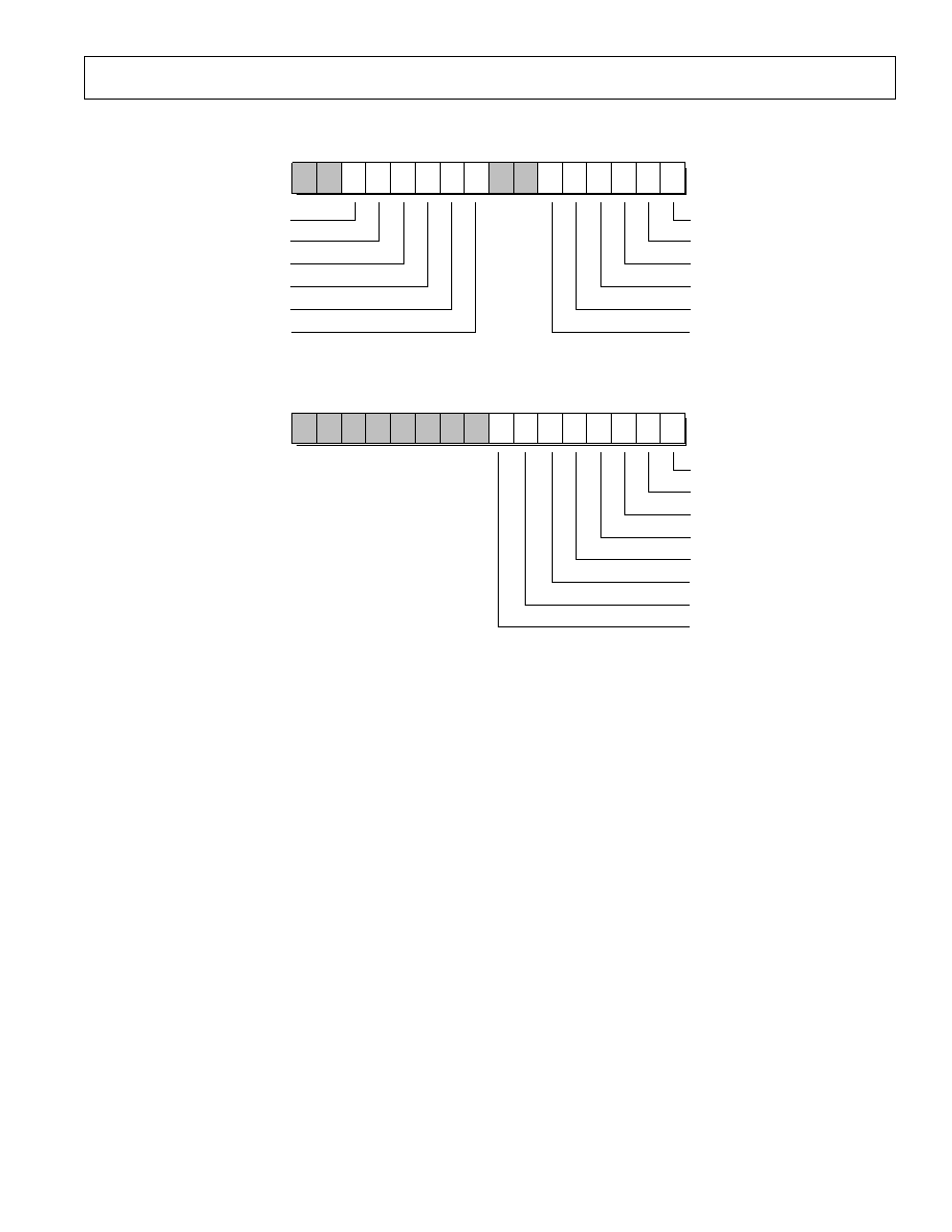
Interrupts
The interrupt controller lets the processor respond to interrupts
and reset with a minimum of overhead. The ADSP-21msp58/59
provides up to three external interrupt input pins, IRQ0, IRQ1,
and IRQ2. IRQ2 is always available as a dedicated pin;
SPORT1 may be reconfigured for IRQ1 and IRQ0 and the flag.
The ADSP-21msp58/59 also supports internal interrupts from
the timer, the host interface port, the serial ports, the analog in-
terface, and the powerdown control circuit. The interrupts are
internally prioritized and individually maskable (except for
powerdown and RESET). The input pins can be programmed
for either level- or edge-sensitivity. The priorities and vector ad-
dresses for the interrupts are shown in Table II; the interrupt
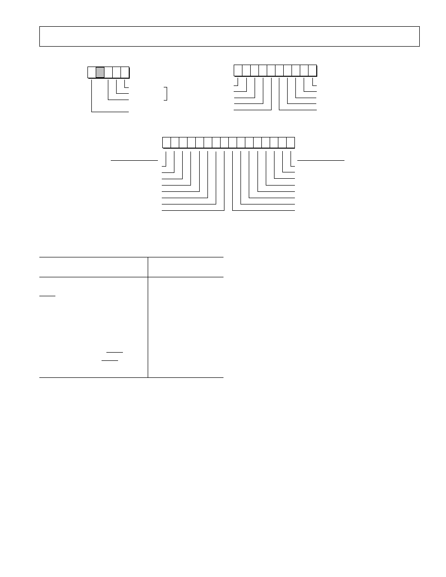
registers are shown in Figure 2.
ADSP-21msp58/59
REV. 0
5
Table II. Interrupt Priority & Interrupt Vector Addresses
Interrupt Vector
Source of Interrupt
Address (Hex)
Reset (or Power-Up with PUCR = 1)
0000 (Highest Priority)
Powerdown (Nonmaskable)
002C
IRQ2
0004
HIP Write
0008
HIP Read
000C
SPORT0 Transmit
0010
SPORT0 Receive
0014
Analog Interface Transmit
0018
Analog Interface Receive
001C
SPORT1 Transmit or (IRQ1)
0020
SPORT1 Receive or (IRQ0)
0024
Timer
0028 (Lowest Priority)
Interrupts can be masked or unmasked with the IMASK regis-
ter. Individual interrupt requests are logically ANDed with the
bits in IMASK; the highest priority unmasked interrupt is then
selected. The powerdown interrupt is non-maskable.
The interrupt control register, ICNTL, allows the external in-
terrupts to be set as either edge- or level-sensitive. Interrupt ser-
vice routines can either be nested (with higher priority interrupts
taking precedence) or be processed sequentially (with only one
interrupt service active at a time).
The interrupt force and clear register, IFC, is a write-only regis-
ter used to force an interrupt or clear a pending edge-sensitive
interrupt.
On-chip stacks preserve the processor status and are automati-
cally maintained during interrupt handling. The stack is twelve
levels deep to allow interrupt nesting.
Register bit values shown in Figure 2 are the default bit values
after reset. If no values are shown, the bits are indeterminate at
reset. Reserved bits are shown in gray; these bits should always
be written with zeros.
0
0
0
0
0
0
0
0
0
0
0
0
0
0
0
0
15 14 13 12 11 10
9
8
7
6
5
4
3
2
1
0
Timer
SPORT1 Receive or IRQ0
SPORT1 Transmit or IRQ1
Analog Receive
Analog Transmit
SPORT0 Receive
SPORT0 Transmit
IRQ2
1 = enable, 0 = disable
INTERRUPT CLEAR
IRQ2
SPORT0 Transmit
SPORT0 Receive
Analog Transmit
Analog Receive
SPORT1 Transmit or IRQ1
SPORT1 Receive or IRQ0
Timer
INTERRUPT FORCE
IFC
0
0
0
0
0
0
0
0
0
0
9
8
7
6
5
4
3
2
1
0
Timer
IRQ0 or SPORT1 Receive
IRQ1 or SPORT1 Transmit
Analog Receive
Analog Transmit
1 = enable, 0 = disable
IRQ2
HIP Write
HIP Read
SPORT0 Transmit
SPORT0 Receive
IMASK
4
3
2
1
0
0
ICNTL
IRQ0 Sensitivity
IRQ1 Sensitivity
IRQ2 Sensitivity
Interrupt Nesting
1 = edge
0 = level
1 = enable, 0 = disable
Figure 2. Interrupt Registers
The following instructions allow global enable or disable servic-
ing of the interrupts (including powerdown), regardless of the
state of IMASK. Disabling the interrupts does not affect
autobuffering.
ENA INTS;
DIS INTS;
Interrupt servicing is enabled on processor reset.
System Interface
Figure 3 shows a basic system configuration with the ADSP-
21msp58/59, two serial devices, a host processor, a boot
EPROM, optional external program and data memories, and an
analog interface. Up to 15K words of data memory and 16K
words of program memory can be supported. Programmable
wait state generation allows the processor to interface easily to
slow memories. The ADSP-21msp58/59 also provides one ex-
ternal interrupt and two serial ports or three external interrupts
and one serial port.
Clock Signals
The ADSP-21msp58/59 CLKIN input may be driven by a crys-
tal or by a TTL-compatible external clock signal.
The CLKIN input may not be halted, changed in frequency
during operation, or operated at any frequency other the one
specified. Operating the ADSP-21msp58/59 at any other fre-
quency changes the analog performance, which is not tested or
supported.
If an external clock is used, it should be a TTL-compatible sig-
nal running at half the instruction rate. The signal should be
connected to the processor's CLKIN input; in this case, the
XTAL input must be left unconnected.
The ADSP-21msp58/59 uses an input clock with a frequency
equal to half the instruction rate; a 13 MHz input clock yields a
38.46 ns processor cycle (which is equivalent to 26 MHz). Nor-
mally, instructions are executed in a single processor cycle.
All device timing is relative to the internal instruction clock rate,
which is indicated by the CLKOUT signal when enabled. The
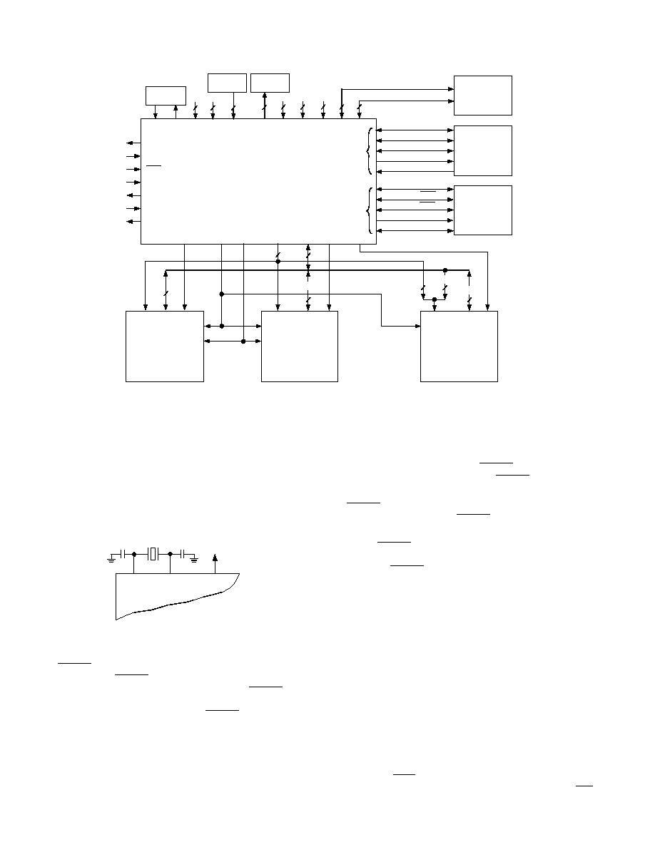
REV. 0
6
ADSP-21msp58/59
CLKIN XTAL V
CC
GND
A
V
DD
GND
HOST
MODE
CLKOUT
RESET
IRQ2
BR
BG
MMAP
FL0
PMS
RD
WR
ADDRESS
DATA
DMS
BMS
HIP
SERIAL
PORT 0
SERIAL
PORT 1
SCLK
RFS
TFS
DT
DR
SCLK
RFS OR
IRQ0
TFS OR
IRQ1
DT OR FO
DR OR FI
24
14
8
7
3
5
4
4
3
2
1
HIP CONTROL
HIP DATA/ADDR
14
2
8
A
D
CS
OE
BOOT
MEMORY
e.g., EPROM
27C64
27C128
27C256
27C512
A
D
CS
OE
WE
DATA
MEMORY &
PERIPHERALS
(OPTIONAL)
24
16
NOTE: The two MSBs of the Boot EPROM Address are also the two MSBs of the Data Bus.
This is only for the 27C256 and 27C512.
ANALOG
INPUT
ANALOG
OUTPUT
CLOCK OR
CRYSTAL
SERIAL DEVICE
(OPTIONAL)
SERIAL DEVICE
(OPTIONAL)
HOST
PROCESSOR
(OPTIONAL)
A
D
CS
OE
WE
PROGRAM
MEMORY
(OPTIONAL)
D
2 3 - 8
D
2 3 - 2 2
D
1 5 - 8
ADSP-21msp58/59
Figure 3. ADSP-21msp58/59 Basic System Configuration
CLKOUT signal is enabled and disabled by the CLKODIS bit
in the SPORT0 Autobuffer Control Register, DM[0x3FF3].
Because the ADSP-21msp58/59 includes an on-chip oscillator
circuit, an external crystal may also be used. The crystal should
be connected across the CLKIN and XTAL pins, with two ca-
pacitors connected as shown in Figure 4. A parallel-resonant,
fundamental frequency, microprocessor-grade crystal should be
used.
CLKIN
XTAL
CLKOUT
ADSP-21msp58/59
Figure 4. External Crystal Connections
Reset
The RESET signal initiates a master reset of the ADSP-
21msp58/59. The RESET signal must be asserted during the
power-up sequence to assure proper initialization. RESET dur-
ing initial power-up must be held long enough to allow the
processor's internal clock to stabilize. If RESET is asserted at
any time after power-up, the clock continues to run and does
not require stabilization time.
The power-up sequence is defined as the total time required for
the crystal oscillator circuit to stabilize after a valid V
DD
is ap-
plied to the processor and for the internal phase-locked loop
(PLL) to lock onto the specific crystal frequency. A minimum of
2000 CLKIN cycles will ensure that the PLL has locked (this
does not, however, include the crystal oscillator start-up time).
During this power-up sequence, the RESET signal should be
held low. On any subsequent resets, the RESET signal must
meet the minimum pulse width specification, t
RSP
.
The RESET input contains some hysteresis; however, if you use
an RC circuit to generate your RESET signal, the use of an ex-
ternal Schmidt trigger is recommended.
The master RESET sets all internal stack pointers to the empty
stack condition, masks all interrupts, and clears the MSTAT
register. When RESET is released, if there is no pending bus re-
quest and the chip is configured for booting (MMAP = 0), the
boot loading sequence is performed. Then the first instruction is
fetched from internal program memory location 0x0000 and ex-
ecution begins.
Program Memory Interface
The on-chip program memory address bus (PMA) and on-chip
program memory data bus (PMD) are multiplexed with the on-
chip data memory buses (DMA, DMD), creating a single exter-
nal data bus and a single external address bus. The data and
address busses are three-stated when the DSP runs from inter-
nal memory. Refer to the ADSP-2100 Family User's Manual,
Chapter 10, "Memory Interface" for a detailed explanation. The
14-bit address bus directly addresses up to 16K words. See
"Program Memory Maps" for details on program memory
addressing.
The program memory data lines are bidirectional. The program
memory select (PMS) signal indicates access to program
memory and can be used as a chip select signal. The write (WR)
signal indicates a write operation and is used as a write strobe.

ADSP-21msp58/59
REV. 0
7
The read (RD) signal indicates a read operation and is used as a
read strobe or output enable signal. An external program
memory access should always be qualified with the PMS signal.
The ADSP-21msp58/59 writes data from its 16-bit registers to
24-bit program memory using the PX register to provide the
lower eight bits. When the processor reads data (not instruc-
tions) from 24-bit program memory to a 16-bit data register, the
lower eight bits are placed in the PX register. The program
memory interface can generate zero to seven wait states for ex-
ternal memory devices; the default is seven wait states after
RESET
.
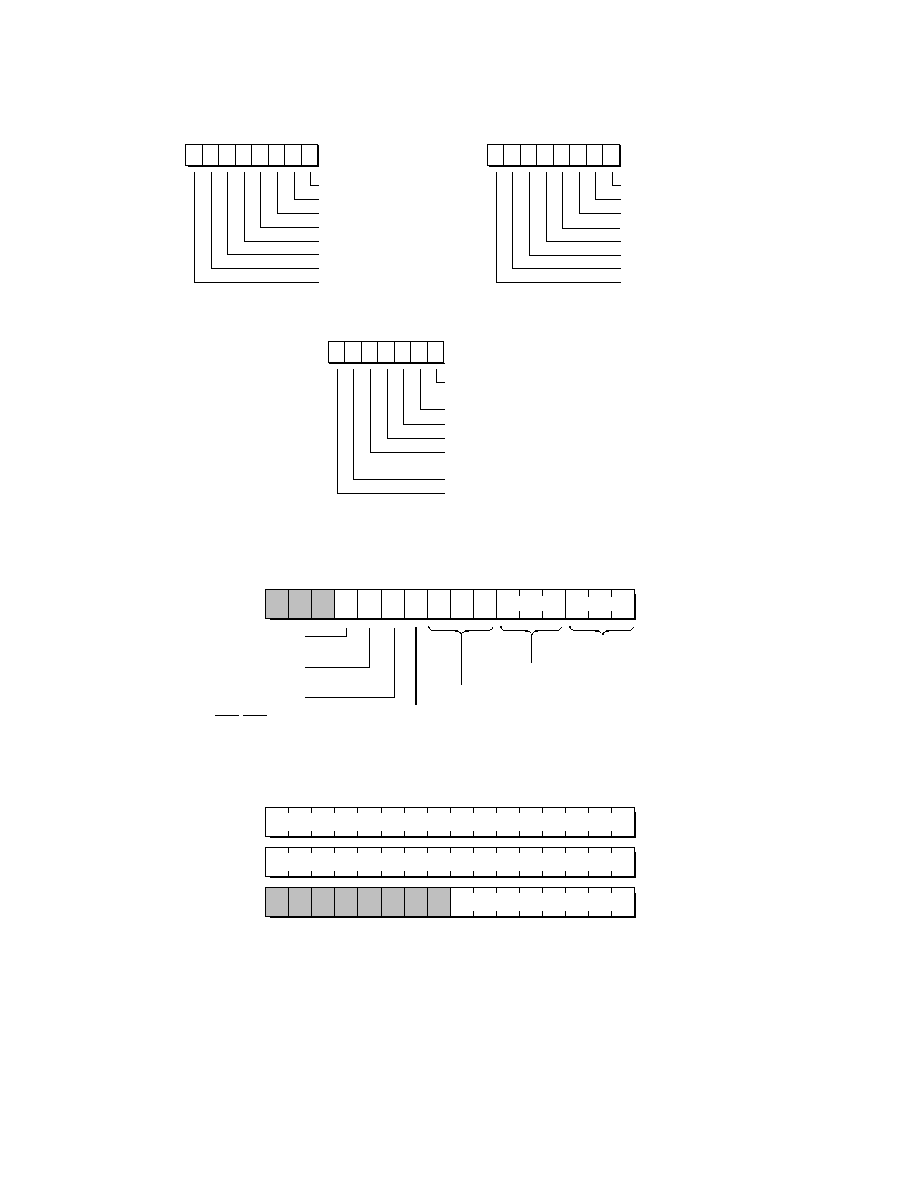
Program Memory Maps
ADSP-21msp58
ADSP-21msp58 Program memory can be mapped in two ways,
depending on the state of the MMAP pin. Figure 5 shows the
two configurations. When MMAP = 0, internal RAM occupies
2K words beginning at address 0x0000; external program
memory uses the remaining 14K words beginning at address
0x0800. In this configuration, the boot loading sequence (de-
scribed in "Boot Memory Interface") is automatically initiated
when RESET is released.
INTERNAL
RAM
LOADED FROM
EXTERNAL
BOOT
MEMORY
EXTERNAL
EXTERNAL
INTERNAL
RAM
NOT LOADED
0000
07FF
0800
3FFF
0000
37FF
3800
3FFF
MMAP=1
MMAP=0
Figure 5. ADSP-21msp58 Program Memory Maps
When MMAP = 1, 14K words of external program memory be-
gin at address 0x0000 and internal RAM is located in the upper
2K words, beginning at address 0x3800. In this configuration,
the boot loading sequence does not take place; execution begins
immediately after RESET.
ADSP-21msp59
The ADSP-21msp59 is functionally identical to the ADSP-
21msp58. The ADSP-21msp59 includes an additional 4K by
24-bit mask programmable ROM (see Figure 6). The ROM
can be used to hold program instructions or data and can be
accessed twice in one instruction cycle if necessary. The ROM
always resides at locations PM[0x0800] through PM[0x17FF]
regardless of the state of the MMAP pin. Sixteen addresses at
the end of ROM (0x17F00x17FF) are reserved for Analog
Devices' use. The ROM is enabled by setting the ROMENABLE
bit in the Data Memory Wait State control register, DM[0x3FFE].
When the ROMENABLE bit is set to 1, addressing program
memory in this range will access the on-chip ROM. When set
to 0, addressing program memory in this range will access exter-
nal program memory. The ROMENABLE bit is set to 0 on
chip reset.
Data Memory Interface
The data memory address bus (DMA) is 14 bits wide. The bi-
directional external data bus is 24 bits wide, with the upper 16
bits used for data memory data (DMD) transfers.
The data memory select (DMS) signal indicates access to data
memory and can be used as a chip select signal. The write (WR)
signal indicates a write operation and can be used as a write
strobe. The read (RD) signal indicates a read operation and can
be used as a read strobe or output enable signal.
The ADSP-21msp58/59 supports memory-mapped I/O, with
the peripherals memory mapped into the data or program
memory address spaces and accessed by the processor in the
same manner.
Data Memory Map
The on-chip data memory RAM resides in the 2K words begin-
ning at address 0x3000, as shown in Figure 7. In addition, data
memory locations from 0x3800 to the end of data memory at
0x3FFF are reserved. Control registers for the system, timer,
INTERNAL
RAM
LOADED FROM
EXTERNAL
BOOT
MEMORY
EXTERNAL
EXTERNAL
INTERNAL
RAM
NOT LOADED
0000
07FF
0800
3FFF
0000
07FF
0800
3FFF
ROM ENABLE = 1
MMAP = 0
EXTERNAL
EXTERNAL
INTERNAL
RAM
NOT LOADED
0000
37FF
3800
3FFF
0000
37FF
3800
3FFF
INTERNAL
MASK
PROGRAMMED
ROM
17FF
1800
17F0 17FF
RESERVED
07FF
0800
17FF
1800
INTERNAL
RAM
LOADED FROM
EXTERNAL
BOOT
MEMORY
INTERNAL
MASK
PROGRAMMED
ROM
17F0 17FF
RESERVED
ROM ENABLE = 0
MMAP = 0
ROM ENABLE = 1
MMAP = 1
ROM ENABLE = 0
MMAP = 1
EXTERNAL
Figure 6. ADSP-21msp59 Program Memory Maps

REV. 0
8
ADSP-21msp58/59
wait-state configuration, host interface port, codec, and serial
port operations are located in this region of memory.
The remaining 12K of data memory is external. External data
memory is divided into three zones, each associated with its own
wait-state generator. By mapping peripherals into different
zones, you can accommodate peripherals with different wait-
state requirements. All zones default to seven wait states after
RESET
.
For compatibility with other ADSP-2100 Family processors, bit
definitions for DWAIT3 and DWAIT4 are shown in the Data
Memory Wait State Control register, but they are not used by
the ADSP-21msp58/59.
12K
EXTERNAL
MEMORY MAPPED
REGISTERS
AND RESERVED
0000
07FF
0800
3FFF
0000
37FF
3800
3FFF
DATA MEMORY
WAIT STATES
DWAIT0
(1K EXTERNAL)
DWAIT1
(1K EXTERNAL)
DWAIT2
(10K EXTERNAL)
NO WAIT STATES
03FF
0400
2FFF
3000
2K
INTERNAL
1K
RESERVED
2FFF
3000
3BFF
3C00
Figure 7. ADSP-21msp58/59 Data Memory Maps
Boot Memory Interface
The ADSP-21msp58/59 can load on-chip memory from exter-
nal boot memory space. The boot memory space consists of
64K by 8-bit space, divided into eight separate 8K by 8-bit
pages. Three bits in the System Control Register select which
page is loaded by the boot memory interface. Another bit in the
System Control Register allows the user to force a boot loading
sequence under software control. Boot loading from Page 0 after
RESET
is initiated automatically if MMAP = 0.
The boot memory interface can generate zero to seven wait
states; it defaults to seven wait states after RESET. This allows
the ADSP-21msp58/59 to boot from a single low cost EPROM
such as a 27C256. Program memory is booted one byte at a
time and converted to 24-bit program memory words.
The BMS and RD signals are used to select and to strobe the
boot memory interface. Only 8-bit data is read over the data
bus, on pins D8D15. To accommodate addressing up to eight
pages of boot memory, the two MSBs of the data bus are used
in the boot memory interface as the two MSBs of the boot
memory address.
The ADSP-2100 Family Assembler and Linker support the cre-
ation of programs and data structures requiring multiple boot
pages during execution.
RD
and WR must always be qualified by PMS, DMS, or BMS
to ensure the correct program, data, or boot memory accessing.
HIP Booting
The ADSP-21msp58/59 can also boot programs through the
Host Interface Port. If BMODE = 1 and MMAP = 0, the
ADSP-21msp58/59 boots from the HIP. If BMODE = 0, the
ADSP-21msp58/59 boots through the data bus (in the same
way as the ADSP-2101), as described above in "Boot Memory
Interface." For additional information about HIP booting, refer
to the ADSP-2100 Family User's Manual, Chapter 7, "Host In-
terface Port."
The ADSP-2100 Family Development Software includes a
utility program called the HIP Splitter. This utility allows the
creation of programs that can be booted through the ADSP-
21msp58/59 HIP, in a similar fashion as EPROM-bootable
programs generated by the PROM Splitter utility.
Bus Request and Bus Grant
The ADSP-21msp58/59 can relinquish control of the data and
address buses to an external device. When the external device
requires access to memory, it asserts the bus request signal
(BR). If the ADSP-21msp58/59 is not performing an external
memory access, it responds to the active BR input in the follow-
ing processor cycle by
· three-stating the data and address buses and the PMS, DMS,
BMS
, RD, and WR output drivers,
· asserting the bus grant (BG) signal, and
· halting program execution.
If GoMode is enabled, the ADSP-21msp58/59 will not halt pro-
gram execution until it encounters an instruction that requires
an external memory access.
If the ADSP-21msp58/59 is performing an external memory ac-
cess when the external device asserts the BR signal, then it will
not three-state the memory interfaces or assert the BG signal
until the cycle after the access is completed, which can be up to
eight cycles later depending on the number of wait states. The
instruction does not need to be completed when the bus is
granted. If a single instruction requires two external memory
accesses, the bus will be granted between the two accesses.
When the BR signal is released, the processor releases the BG
signal, which reenables the output drivers, and continues pro-
gram execution from the point where it stopped.
The bus request feature operates at all times, including when
the processor is booting and when RESET is active.
LOW POWER OPERATION
The ADSP-21msp58/59 has three low power modes that signifi-
cantly reduce the power dissipation when the device operates
under standby conditions. These modes are:
· Powerdown
· Idle
· Slow Idle
The CLKOUT pin may also be disabled to reduce external
power dissipation. The CLKOUT pin is controlled by Bit 14 of
SPORT0 Autobuffer Control Register, DM[0x3FF3].
Powerdown
The ADSP-21msp58/59 has a low power feature that lets the
processors enter a very low power dormant state through hard-
ware or software control. Here is a brief list of powerdown fea-
tures. Refer to the ADSP-2100 Family User's Manual, Chapter 9,

ADSP-21msp58/59
REV. 0
9
"System Interface" for detailed information about the power-
down feature.
· Powerdown mode holds the processor in CMOS standby with
a maximum current of less than 100
µ
A in some modes.
· Quick recovery from powerdown. In some modes, the proces-
sor can begin executing instructions in less than 100 CLKIN
cycles.
· Support for an externally generated TTL or CMOS processor
clock. The external clock can continue running during
powerdown without affecting the lowest power rating and 100
CLKIN cycle recovery.
· Support for crystal operation includes disabling the oscillator
to save power (the processor automatically waits 4096 CLKIN
cycles for the crystal oscillator to start and stabilize), and
letting the oscillator run to allow 100 CLKIN cycle start-up.
· Powerdown is initiated by either the powerdown pin (PWD)
or the software powerdown force bit.
· Interrupt support allows an unlimited number of instructions
to be executed before optionally powering down. The power-
down interrupt also can be used as a non-maskable, edge-
sensitive interrupt.
· Context clear/save control lets the processor continue where it
left off or start with a clean context when leaving the power-
down state.
· The RESET pin also can be used to terminate powerdown,
and the host software reset feature can be used to terminate
powerdown under certain conditions.
· Setting the CLKODIS bit (Bit 14 of the SPORT0 Autobuffer
Control Register [0x3FF3]) disables the CLKOUT pin during
powerdown.
Idle
When the ADSP-21msp58/59 is in the Idle Mode, the processor
waits indefinitely in a low power state until an interrupt occurs.
When an unmasked interrupt occurs, it is serviced; execution
then continues with the instruction following the IDLE instruction.
Slow Idle
The IDLE instruction is enhanced on the ADSP-21msp58/59 to
let the processor's internal clock signal be slowed, further reduc-
ing power consumption. The reduced clock frequency, a pro-
grammable fraction of the normal clock rate, is specified by a
selectable divisor given in the IDLE instruction. The format of
the instruction is
IDLE (n);
where n = 16, 32, 64, or 128. This instruction keeps the proces-
sor fully functional, but operating at the slower clock rate. While
it is in this state, the processor's other internal clock signals,
such as SCLK, and timer clock, are reduced by the same ratio.
CLKOUT remains at the normal rate; it is not reduced. The de-
fault form of the instruction, when no clock divisor is given, is
the standard IDLE instruction.
When the IDLE (n) instruction is used, it effectively slows down
the processor's internal clock and thus its response time to in-
coming interruptsthe 1-cycle response time of the standard
idle state is increased by n, the clock divisor. When an enabled
interrupt is received, the ADSP-21msp58/59 remains in the idle
state for up to a maximum of n processor cycles (n = 16, 32, 64,
or 128) before resuming normal operation.
When the IDLE (n) instruction is used in systems that have an
externally generated serial clock (SCLK), the serial clock rate
may be faster than the processor's reduced internal clock rate.
Under these conditions, interrupts must not be generated at a
faster rate than can be serviced, due to the additional time the
processor takes to come out of the idle state (a maximum of n
processor cycles).
Standalone ROM Execution (ADSP-21msp59 Only)
When the MMAP and BMODE pins both are set to 1, the
ROM is automatically enabled and execution commences from
program memory location 0x0800 at the start of ROM. This
feature lets an embedded design operate without external
memory components. To operate in this mode, the ROM coded
program must copy an interrupt vector table to the appropriate
locations in program memory RAM. In this mode, the ROM
enable bit defaults to 1 during reset.
Table III. Boot Summary Table
BMODE = 0
BMODE = 1
MMAP = 0
Boot from EPROM,
Boot from HIP, then
then execution starts
execution starts at
at internal RAM
internal RAM location
location 0x0000
0x0000
MMAP = 1
No booting, execution
Stand Alone Mode,
starts at external memory execution starts at
location 0x0000
internal ROM location
0x0800
Ordering Procedure For ADSP-21msp59 ROM Processors
To place an order for a custom ROM-coded ADSP-21msp59
processor, you must:
1. Complete the following forms contained in the ADSP ROM
Ordering Package, available from your Analog Devices sales
representative:
ADSP-21msp59 ROM Specification Form
ROM Release Agreement
ROM NRE Agreement & Minimum Quantity Order (MQO)
Acceptance Agreement for Preproduction ROM Products
2. Return the forms to Analog Devices along with two copies of
the Memory Image File (.EXE file) of your ROM code. The
files must be supplied on two 3.5" or 5.25" floppy disks for
the IBM PC (DOS 2.01 or higher).
3. Place a purchase order with Analog Devices for nonrecurring
engineering changes (NRE) associated with ROM product
development.
After this information is received, it is entered into Analog
Devices' ROM Manager System that assigns a custom ROM
model number to the product. This model number will be
branded on all prototype and production units manufactured to
these specifications.
To minimize the risk of code being altered during this process,
Analog Devices verifies that the .EXE files on both floppy disks
are identical, and recalculates the checksums for the .EXE file
entered into the ROM Manager System. The checksum data, in
the form of a ROM Memory Map, a hard copy of the .EXE file,
and a ROM Data Verification form are returned to you for
inspection.
REV. 0
10
ADSP-21msp58/59
A signed ROM Verification Form and a purchase order for pro-
duction units are required prior to any product being manufac-
tured. Prototype units may be applied toward the minimum
order quantity.
Upon completion of prototype manufacture, Analog Devices
will ship prototype units and a delivery schedule update for pro-
duction units. An invoice against your purchase order for the
NRE charges is issued at this time.
There is a charge for each ROM mask generated and a mini-
mum order quantity. Consult your sales representative for de-
tails. A separate order must be placed for parts of a specific
package type, temperature range, and speed grade.
ANALOG INTERFACE
The analog interface contains encoding circuitry (ADC), decod-
ing circuitry (DAC), and processor interface logic. A block dia-
gram of the ADSP-21msp58/59 analog section is shown in
Figure 8.
The analog interface is configured through the Analog Control
Register and the Analog Autobuffer/Powerdown Register (refer
to "ADSP-21msp58/59 Registers"). The Analog Control Regis-
ter DM[0x3FEE] configures the programmable gain stages, the
analog input multiplexer, and the analog interface powerdown
state. Note that the unused bits must be cleared to zero.
16
OUTPUT
DIFFERENTIAL AMP
VIN
NORM
VIN
AUX
DECOUPLE
REF_FILTER
V
REF
VOUT
P
VOUT
N
MUX
DAC
PGA
ANALOG
SMOOTHING
FILTER
BUF
VOLTAGE
REFERENCE
ADC
PGA
16-BIT
SIGMA-
DELTA
DAC
16-BIT
SIGMA-
DELTA
ADC
PROCESSOR
INTERFACE
Figure 8. Analog Interface Block Diagram
A/D Conversion
The A/D conversion circuitry of the analog interface consists of
an analog multiplexer, a programmable gain amplifier (ADC
PGA), and a 16-bit sigma-delta analog-to-digital converter
(ADC).
Analog Input Multiplexer and Amplifiers
The analog multiplexer selects either the NORM or AUX input
to the ADC's sigma-delta modulator. The inputs should be ac
coupled.
The ADC PGA may be used to additionally increase the signal
level by +6 dB, +20 dB, or +26 dB. This gain is selected by bit
9 and bit 0 (IG0, IG1) of the analog control register. Input sig-
nal level to the sigma-delta ADC should not exceed the V
INMAX
specification.
Analog-To-Digital Converter
The analog interface's analog-to-digital converter consists of a
4th-order analog sigma-delta modulator, an anti-aliasing deci-
mation filter, and an optional digital high-pass filter. For a detailed
description of the ADC components, refer to the ADSP-2100
Family User's Manual, Chapter 8, "Analog Interface."
Bit 10 of the Analog Control Register (0x3FEE) may be set to
add an offset to the input of the ADC sigma-delta converter.
This offset moves ADC sigma-delta idle tones out of the 4.0
kHz speech band range. This added offset must be removed by
the ADC high-pass filter. Therefore, the high-pass filter must be
inserted when you use the offset feature.
D/A Conversion
The D/A conversion circuitry of the analog interface consists of
a sigma-delta digital-to-analog converter (DAC), an analog
smoothing filter, a programmable gain amplifier (DAC PGA),
and a differential output amplifier.
Digital-to-Analog Converter
The digital-to-analog converter consists of an optional digital
high-pass filter, an anti-imaging interpolation filter, and a
sigma-delta modulator. The digital filters and the sigma-delta
modulator have the same characteristics as the filters and
modulator of the ADC. For detailed description of the DAC
components, refer to the ADSP-2100 Family User's Manual,
Chapter 8, "Analog Interface."
Analog Smoothing Filter and Programmable Gain Amplifier
The analog smoothing filter consists of a 3rd-order switched ca-
pacitor filter with a 3 dB point at approximately 25 kHz.
The DAC's programmable gain amplifier (DAC PGA) can be
used to adjust the output signal level by 15 dB to +6 dB in
3 dB increments. This gain is selected by bits 24 (OG0, OG1,
OG2) of the analog control register.
Differential Output Amplifier
The analog output signal (VOUT
P
, VOUT
N
) is produced by a
differential amplifier. The differential amplifier meets specifica-
tions for loads greater than 2 k
and has a maximum differen-
tial output swing of
±
3.156 V peak-to-peak (3.17 dBm0). The
DAC will drive loads smaller than 2 k
, but with degraded
performance.
The output signal is dc-biased to the on-chip voltage reference
(V
REF
) and can be ac-coupled directly to a load or dc-coupled to
an external amplifier.
The VOUT
P
, VOUT
N
output must be used as a differential sig-
nal otherwise performance will be severely compromised. Do
not use either pin as a single-ended output.
OPERATING THE ANALOG INTERFACE
The analog interface is operated with several memory-mapped
control and data registers. The ADC and DAC I/O data is re-
ceived and transmitted through two memory-mapped data regis-
ters. The data can also be autobuffered directly into (or from)
on-chip memory. In both cases, the I/O processing is interrupt
driven; two interrupts are dedicated to the analog interface, one
for the ADC receive data and one for the DAC transmit data.
The ADSP-21msp58/59 must have an input clock frequency of
13 MHz. At this frequency, analog-to-digital and digital-to-ana-
log converted data is transmitted at an 8 kHz rate with a single
16-bit word transmitted every 125
µ
s.
For detailed information about the analog interface, refer to the
ADSP-2100 Family User's Manual, Chapter 8, "Analog Interface."
ADSP-21msp58/59
REV. 0
11
Autobuffering
In some applications, it is advantageous to perform block data
transfers between the analog converters and processor memory.
Analog interface autobuffering enables the automatic transfer of
data blocks directly from the ADC to on-chip processor data
memory or from on-chip processor data memory directly to the
DAC.
ADC and DAC Interrupts
The analog interface generates two interrupts that signal either:
(1) a 16-bit, 8 kHz analog-to-digital or digital-to-analog conver-
sion has been completed, or (2) an autobuffer block transfer
has been completed (i.e., the data buffer contents have been
received or transferred).
When an analog interrupt occurs, the processor vectors to the
addresses listed in Table II, Interrupt Priority & Interrupt Vector
Addresses.
The ADC receive and DAC transmit interrupts occur at an
8 kHz rate, indicating when the data registers should be ac-
cessed. On the receive side, the ADC interrupt is generated each
time an A/D conversion cycle is completed and the 16-bit data
word is available in the ADC receive register. On the transmit
side, the DAC interrupt is generated each time an D/A conver-
sion cycle is completed and the DAC transmit register is ready
for the next 16-bit data word.
Both interrupts are generated simultaneously at an 8 kHz rate,
occurring every 3250 instruction cycles with a 13 MHz internal
processor clock. The interrupts are generated continuously,
starting when the analog interface is powered up by setting the
APWD bits (Bits 5 and 6) to one in the analog control register.
Because both interrupts occur simultaneously, only one should
be enabled (in IMASK) to vector to a single service routine that
handles transmit and receive data. However, when using
autobuffer transfers, both interrupts should be enabled.
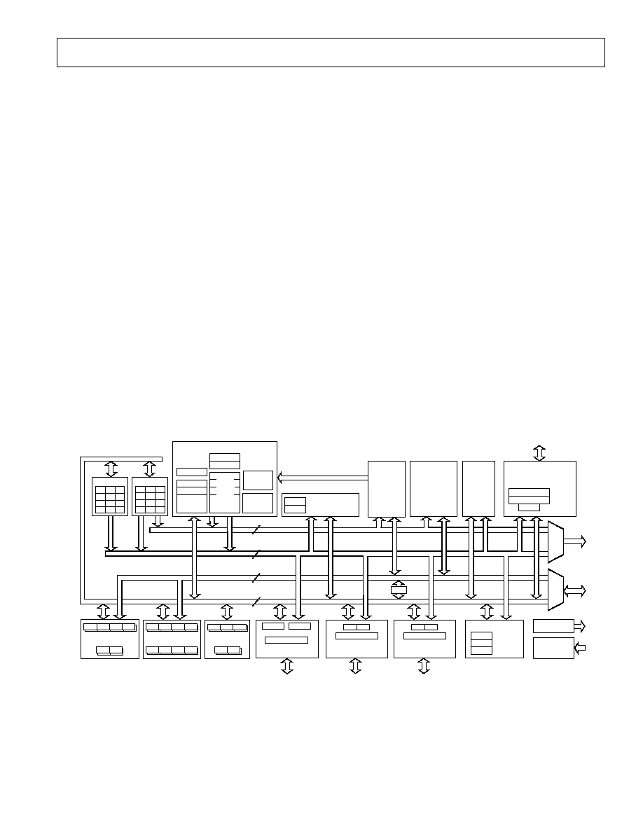
ADSP-21msp58/59 REGISTERS
Figure 9 summarizes the ADSP-21msp58/59 registers. Some
registers store values. For example, AX0 stores an ALU oper-
and; I4 stores a DAG2 pointer. Other registers consist of control
bits and fields, or status flags. For example ASTAT contains
status flags from arithmetic operations, and fields in DWAIT
control the number of wait states for different zones of data
memory.
A secondary set of registers in all computational units allows a
single-cycle context switch.
The bit and field definitions for control and status registers are
given in the rest of this section, except IMASK, ICNTL, and
IFC, which are defined earlier in this data sheet. The system
control register, DWAIT register, timer registers, HIP control
registers, HIP data registers, and SPORT control registers are
all mapped into data memory locations; that is, you access these
registers by reading and writing data memory locations rather
than register names. The particular data memory address is
shown with each memory-mapped register.
Register bit values shown on the following pages are the default
bit values after reset. If no values are shown, the bits are indeter-
minate at reset. Reserved bits are shown in gray; these bits
should always be written with zeros.
POWERDOWN
CONTROL
LOGIC
TX1
RX1
0x3FF2-0x3FEF
CONTROL REGISTERS
SPORT 1
MX0 MX1 MY0 MY1
MR0 MR1 MR2 MF
MAC
AX0 AX1 AY0 AY1
AF
AR
ALU
S I
SE
SB
SHIFTER
SR1
SR0
DAC
ADC
CONTROL REGISTERS
ANALOG INTERFACE
0x3FEC
0x3FED
0x3FEE-0x3FEF
0x3FFD
0x3FFC
0x3FFB
TPERIOD
TCOUNT
TSCALE
TIMER
I0
I1
I2
I3
M0
M1
M2
M3
L0
L1
L2
L3
DAG 1
0x3FFF
0x3FFE
SYSTEM CONTROL
DM WAIT CONTROL
PROGRAM
ROM
4K x 24
ADSP-21msp59
ONLY
DATA
SRAM
2K x 16
0x3FE0-0x3FE5
0x3FE6-0x3FE7
0x3FE8
DATA
STATUS
HMASK
HOST
INTERFACE
PORT
DMD BUS
16
24
14
14
PMD BUS
DMA BUS
PMA BUS
I4
I5
I6
I7
M4
M5
M6
M7
L4
L5
L6
L7
DAG 2
SSTAT
COUNT
STACK
4 x 14
OWRCNTR
CNTR
IMASK
MSTAT
ASTAT
STATUS
STACK
12 x 25
LOOP
STACK
4 x 18
PC
STACK
16 x 14
PROGRAM SEQUENCER
ICNTL
IFC
PROGRAM
SRAM
2K x 24
PX
FLAG
TX0
RX0
0x3FFA-0x3FF3
CONTROL REGISTERS
SPORT 0
Figure 9. ADSP-21msp58/59 Registers
REV. 0
12
ADSP-21msp58/59
0
0
0
0
0
1
0
0
0
0
1
1
1
1
1
1
15
14
13
12
11
10
9
8
7
6
5
4
3
2
1
0
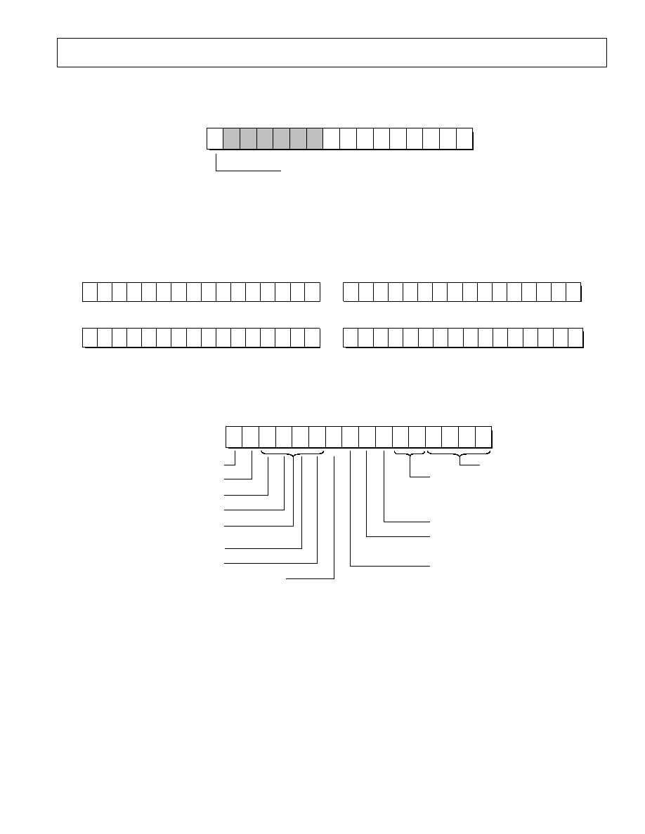
System Control Register
0x3FFF
SPORT0 Enable
1 = enabled, 0 = disabled
SPORT1 Enable
1 = enabled, 0 = disabled
SPORT1 Configure
1 = serial port
0 = FI, FO,
IRQ0
,
IRQ1
, SCLK
BFORCE
Boot Force Bit
BPAGE
Boot Page Select
BWAIT
Boot Wait States
PWAIT
Program Memory
Wait States
AZ ALU Result Zero
AN ALU Result Negative
AV ALU Overflow
AC ALU Carry
AS ALU X Input Sign
AQ ALU Quotient
MV MAC Overflow
SS Shifter Input Sign
7
6
5
4
3
2
1
0
0
0
0
0
0
0
0
0
ASTAT
PC Stack Empty
PC Stack Overflow
Count Stack Empty
Count Stack Overflow
Status Stack Empty
Status Stack Overflow
Loop Stack Empty
Loop Stack Overflow
7
6
5
4
3
2
1
0
0
1
0
1
0
1
0
1
SSTAT (Read -Only)
Data Register Bank Select
0 = primary, 1 = secondary
Bit Reverse Mode Enable (DAG1)
ALU Overflow Latch Mode Enable
AR Saturation Mode Enable
MAC Result Placement
0 = fractional, 1 = integer
Timer Enable
Go Mode Enable
6
5
4
3
2
1
0
0
0
0
0
0
0
0
MSTAT
TPERIOD Period Register
15
14
13
12
11
10
9
8
7
6
5
4
3
2
1
0
TCOUNT Counter Register
0
0
0
0
0
0
0
0
TCOUNT Scaling Register
0x3FFD
0x3FFC
0x3FFB
Timer Registers
Control Registers
ADSP-21msp58/59
REV. 0
13
0
0
0
0
0
0
0
0
0
0
0
0
0
0
0
0
15
14
13
12
11
10
9
8
7
6
5
4
3
2
1
0
SPORT0 Control Register
0x3FF6
Multichannel Enable MCE
Internal Serial Clock Generation ISCLK
Receive Frame Sync Required RFSR
Receive Frame Sync Width RFSW
Multichannel Frame Delay MFD
Only If Multichannel Mode Enabled
Transmit Frame Sync Required TFSR
Transmit Frame Sync Width TFSW
ITFS Internal Transmit Frame Sync Enable
(or MCL Multichannel Length; 1 = 32 words, 0 = 24 words
Only If Multichannel Mode Enabled )
SLEN Serial Word Length
DTYPE Data Format
00 = right justify, zero-fill unused MSBs
01 = right justify, sign extend into unused MSBs
10 = compand using µ-law
11 = compand using A-law
INVRFS Invert Receive Frame Sync
INVTFS Invert Transmit Frame Sync
(or INVTDV Invert Transmit Data Valid
Only If Multichannel Mode Enabled )
IRFS Internal Receive Frame Sync Enable
31
30
29
28
27
26
25
24
23
22
21
20
19
18
17
16
15
14
13 12
11 10
9
8
7
6
5
4
3
2
1
0
15
14
13
12
11
10
9
8
7
6
5
4
3
2
1
0
31
30
29
28
27
26
25
24
23
22
21
20
19
18
17
16
SPORT0 Multichannel Receive Word Enable Registers
1 = Channel Enabled
0 = Channel Ignored
0x3FFA
0x3FF9
0x3FF8
0x3FF7
SPORT0 Multichannel Transmit Word Enable Registers
1 = Channel Enabled
0 = Channel Ignored
0
0
0
0
0
0
0
1
1
1
1
1
1
1
1
1
15
14
13
12
11
10
9
8
7
6
5
4
3
2
1
0
ROM Enable/Data Memory Wait State
Control Register
0x3FFE
DWAIT4
DWAIT3
DWAIT2
DWAIT1
DWAIT0
ROM enable (ADSP-21msp59)
1 = enable
0 = disable
Control Registers
REV. 0
14
ADSP-21msp58/59
0
0
0
0
0
0
15
14
13
12
11
10
9
8
7
6
5
4
3
2
1
0
SPORT0 Autobuffer Control Register
0x3FF3
CLKODIS
CLKOUT Disable Control Bit
BIASRND
MAC Biased Rounding Control Bit
TIREG
Transmit Autobuffer I Register
RBUF
Receive Autobuffering Enable
TBUF
Transmit Autobuffering Enable
RMREG
Receive Autobuffer M Register
RIREG
Receive Autobuffer I Register
TMREG
Transmit Autobuffer M Register
15
14
13
12
11
10
9
8
7
6
5
4
3
2
1
0
SPORT0 SCLKDIV
Serial Clock Divide Modulus
0x3FF5
15
14
13
12
11
10
9
8
7
6
5
4
3
2
1
0
0
0
0
0
0
0
0
0
0
0
0
0
0
0
0
SPORT1 Control Register
0x3FF2
Flag Out (Read Only)
Internal Serial Clock Generation ISCLK
Receive Frame Sync Required RFSR
Receive Frame Sync Width RFSW
Transmit Frame Sync Required TFSR
Transmit Frame Sync Width TFSW
ITFS Internal Transmit Frame Sync Enable
SLEN Serial Word Length
DTYPE Data Format
00 = right justify, zero-fill unused MSBs
01 = right justify, sign extend into unused MSBs
10 = compand using µ-law
11 = compand using A-law
INVRFS Invert Receive Frame Sync
INVTFS Invert Transmit Frame Sync
IRFS Internal Receive Frame Sync Enable
15
14
13
12
11
10
9
8
7
6
5
4
3
2
1
0
SPORT0 RFSDIV
Receive Frame Sync Divide Modulus
0x3FF4
Control Registers
ADSP-21msp58/59
REV. 0
15
0
0
0
0
0
0
0
0
0
0
0
0
0
0
0
0
15
14
13
12
11
10
9
8
7
6
5
4
3
2
1
0
HMASK Register
0x3FE8
Host HDR5 Read
Host HDR4 Read
Host HDR3 Read
Host HDR2 Read
Host HDR1 Read
Host HDR0 Read
Host HDR0 Write
Host HDR1 Write
Host HDR2 Write
Host HDR3 Write
Host HDR4 Write
Host HDR5 Write
Interrupt Enables
1 = Enable
0 = Disable
0
0
0
0
0
0
15
14
13
12
11
10
9
8
7
6
5
4
3
2
1
0
Analog Autobuffer/Powerdown Control Register
0x3FEF
XTALDIS
XTAL Pin Disable During Powerdown
1 = disabled, 0 = enabled
(XTAL pin should be disabled when
no external crystal is connected)
XTALDELAY
Delay Startup From Powerdown 4096 Cycles
1 = delay, 0 = no delay
(use delay to let internal phase locked
loop or external oscillator stabilize)
PDFORCE
Powerdown Force
1 = force processor to vector to
powerdown interrupt
PUCR
Powerup Context Reset
1 = soft reset, 0 = resume execution
ARBUF
ADC Receive Autobuffer Enable
ATBUF
DAC Transmit Autobuffer Enable
ARMREG
Receive M Register
ARIREG
Receive I Register
ATMREG
Transmit M Register
ATIREG
Transmit I Register
15
14
13
12
11
10
9
8
7
6
5
4
3
2
1
0
SPORT1 SCLKDIV
Serial Clock Divide Modulus
0x3FF1
15
14
13
12
11
10
9
8
7
6
5
4
3
2
1
0
SPORT1 RFSDIV
Receive Frame Sync Divide Modulus
0x3FF0
Control Registers
REV. 0
16
ADSP-21msp58/59
0
0
0
0
0
0
0
0
0
0
0
0
0
0
0
0
15
14
13
12
11
10
9
8
7
6
5
4
3
2
1
0
Analog Control Register
0x3FEE
ADC Offset
IG0
ADC Input Gain
DABY
DAC High Pass Filter Bypass
1 = bypass, 0 = insert
ADBY
ADC High Pass Filter Bypass
1 = bypass, 0 = insert
APWD
Analog Interface Powerdown
0 = powerdown, 1 = enable
(set both bits to 1
to enable analog interface)
IG1
ADC Input Gain
IMS
ADC Input Multiplexer Select
1 = AUX input, 0 = NORM input
OG2, OG1, OG0
DAC Output Gain (for PGA)
OG2
OG1
OG0
0dB
+6dB
+20dB
+26dB
IG1
0
0
1
1
IG0
0
1
0
1
Gain
+6dB
+3dB
0dB
3dB
6dB
9dB
12dB
15dB
IG2
0
0
0
0
1
1
1
1
IG1
0
0
1
1
0
0
1
1
IG1
0
1
0
1
0
1
0
1
Gain
IG0, IG1
ADC Input Gain (for PGA)
All bits are set to 0 at processor reset.
(Reserved bits 1115 must always be set to 0)
15
14
13
12
11
10
9
8
7
6
5
4
3
2
1
0
DM(0x3FED)
ADC Receive
15
14
13
12
11
10
9
8
7
6
5
4
3
2
1
0
DM(0x3FEC)
DAC Transmit
15 14 13 12 11 10
9
8
7
6
5
4
3
2
1
0
0x3FE5
HIP Data Registers
HDR5
0x3FE4
0x3FE3
0x3FE2
0x3FE1
0x3FE0
HDR4
HDR3
HDR2
HDR1
HDR0
Control Registers
ADSP-21msp58/59
REV. 0
17
0
0
0
0
0
0
0
0
1
0
0
0
0
0
0
0
15
14
13
12
11
10
9
8
7
6
5
4
3
2
1
0
HSR7
0x3FE7
ADSP-21msp58/59 HDR0 Write
ADSP-21msp58/59 HDR1 Write
ADSP-21msp58/59 HDR2 Write
ADSP-21msp58/59 HDR3 Write
ADSP-21msp58/59 HDR4 Write
ADSP-21msp58/59 HDR5 Write
Overwrite Mode
Software Reset
0
0
0
0
0
0
0
0
0
0
0
0
0
0
0
0
15
14
13
12
11
10
9
8
7
6
5
4
3
2
1
0
HSR6
0x3FE6
ADSP-21msp58/59 HDR5 Write
ADSP-21msp58/59 HDR4 Write
ADSP-21msp58/59 HDR3 Write
ADSP-21msp58/59 HDR2 Write
ADSP-21msp58/59 HDR1 Write
ADSP-21msp58/59 HDR0 Write
Host HDR0 Write
Host HDR1 Write
Host HDR2 Write
Host HDR3 Write
Host HDR4 Write
Host HDR5 Write
Control Registers
ADSP-21msp58/59 EXTENDED INSTRUCTION SET
The ADSP-21msp58/59 has a number of additional instruc-
tions beyond the standard ADSP-2100 Family instruction set.
These additional instructions and mathematical operations are
described below.
Slow IDLE
Slow IDLE allows slowing the processor's internal clock by a
factor of 16, 32, 64, or 128 during IDLE. The instruction
source code is specified as follows:
Syntax:
IDLE (n);
Permissible Values for n
16, 32, 64, 128
Examples:
IDLE;
IDLE (16);
Description: The IDLE instruction causes the processor to
wait indefinitely in a low power state until an in-
terrupt occurs. When an unmasked interrupt oc-
curs, it is serviced; execution then continues with
the instruction following the IDLE instruction.
The optional value provides a "slow idle" fea-
ture; slowing the clock down by the factor set
with the value.
Interrupt Enable and Disable Instructions
The ADSP-21msp58/59 supports an interrupt enable instruc-
tion and interrupt disable instruction. Interrupts are enabled by
default at reset. The interrupt enable instruction source code is
specified as follows:
INSTRUCTION SET DESCRIPTION
The ADSP-21msp58/59 assembly language instruction set has
an algebraic syntax that was designed for ease of coding and
readability. The assembly language, which takes full advantage
of the processor's unique architecture, offers the following
benefits:
· The algebraic syntax eliminates the need to remember cryptic
assembler mnemonics. For example, a typical arithmetic add
instruction, such as AR = AX0 + AY0, resembles a simple
equation.
· Every instruction assembles into a single 24-bit word and
executes in a single cycle.
·The syntax is a superset of the ADSP-2100 Family assembly
language and is completely source and object code compatible
with other family members. Programs may, however, need to
be relocated to utilize internal memory and conform to the
ADSP-21msp58/59 interrupt vector and reset vector map.
· Sixteen condition codes are available. For conditional jump,
call, return, or arithmetic instructions, the condition can be
checked and the operation executed in the same instruction
cycle.
· Multifunction instructions allow parallel execution of an
arithmetic instruction with up to two fetches and one write to
processor memory space during a single instruction cycle.
Consult the ADSP-2100 Family User's Manual for a complete
description of the syntax and an instruction set reference.

REV. 0
18
ADSP-21msp58/59
Syntax:
ENA INTS;
Description: Executing the ENA INTS instruction allows all
unmasked interrupts to be serviced again.
The interrupt disable instruction source code is specified as
follows:
Syntax:
DIS INTS;
Description: Reset enables interrupt servicing. Executing the
DIS INTS instruction causes all interrupts to be
masked without changing the contents of the
IMASK register. Disabling interrupts does not
affect the autobuffer circuitry, which will operate
normally whether or not interrupts are enabled.
The disable interrupt instruction masks all user
interrupts including the powerdown interrupt.
Extended ALU and Multiplier Operations
The following extended computation operations are available
only on the ADSP-21msp58/59 processor. The term "base in-
struction set" refers to the computations and instructions avail-
able on all ADSP-21xx processors.
Additional Constants for ALU Operations
A new set of numerical constants may be used in all nonmulti-
function ALU operations (except DIVS and DIVQ) using both
X and Y operands. The instruction source code is specified as
follows:
Syntax: [IF condition]
AR
= xop function
yop
AF
constant
Permissible xops
AX0, AX1, AR, MR0, MR1, MR2, SR0, SR1
Permissible functions
ADD/ADD with CARRY, SUBTRACT XY/SUBTRACT X
Y with BORROW, SUBTRACT YX/SUBTRACT YX with
BORROW, AND, OR, XOR
Permissible yops (base instruction set)
AY0, AY1, AF
Permissible yops and constants (extended instruction set)
AY0, AY1, AF, 0, 1, 2, 4, 8, 16, 32, 64, 128, 256, 512, 1024,
2048, 4096, 8192, 16384, 32767, 2, 3, 5, 9, 17, 33, 65,
129, 257, 513, 1025, 2049, 4097, 8193, 16385, 32768
Examples:
AR = AR+1;
AR = MR1 - 33;
IF GT AF = AX1 OR 16;
Description: Test the optional condition and, if true, perform
the specified function. If false then perform a no-
operation. Omitting the condition performs the
function unconditionally. The operands are con-
tained in the data registers specified in the in-
struction or optionally a constant may be used.
Additional Constants for ALU PASS Operation
A new set of numerical constants may be used in the PASS in-
struction. The instruction source code is specified as follows:
Syntax:
[IF condition]
AR
= pass
yop
AF
constant
Permissible yops (base instruction set)
AY0, AY1, AF
Permissible yops and constants (extended instruction set)
AY0, AY1, AF, 0, 1, 2, 3, 4, 5, 7, 8, 9, 15, 16, 17, 31, 32, 33,
63, 64, 65, 127, 128, 129, 255, 256, 257, 511, 512, 513, 1023,
1024, 1025, 2047, 2048, 2049, 4095, 4096, 4097, 8191, 8192,
8193, 16383, 16384, 16385, 32766, 32767, 1, 2, 3, 4, 5,
6, 8, 9, 10, 16, 17, 18, 32, 33, 34, 64, 65, 66, 128,
129, 130, 256, 257, 258, 512, 513, 514, 1024, 1025,
1026, 2048, 2049, 2050, 4096, 4097, 4098, 8192, 8193,
8194, 16384, 16385, 16386, 32767, 32768
Examples:
IF GE AR = PASS AY0;
IF EQ AF = PASS 1025;
Description: Test the optional condition and, if true, pass the
source operand unmodified through the ALU
block and store in the destination location. If the
condition is not true, perform a no-operation.
Omitting the condition performs the pass uncon-
ditionally. The source operand is contained in
the data registers specified in the instruction or
optional constant.
The PASS instruction performs the transfer to the
AR register and affect the status flag; this instruc-
tion is different from a register move operation
which does not affect any status flags. PASS 0 is
one method of clearing AR. PASS 0 can also be
combined in a multifunction instruction in con-
junction with memory reads and writes to clear AR.
Note:
The ALU status flags (in the ASTAT register)
are not defined for the execution of this instruc-
tion when using the constant values other than 0,
1, and 1.
ALU Bit Operations
The additional constants for ALU operations allow you to code
bit test, set, clear, and toggle operations through careful choice
of the constant and ALU function. For streamlined programming,
the source code for these operations can also be specified as:
Syntax: [IF condition]
AR
=
TSTBIT n of xop;
AF
SETBIT n of xop;
CLBIT n of xop;
TGBIT n of xop;
Permissible xops
AX0, AX1, AR, MR0, MR1, MR2, SR0, SR1
Permissible n Values (0 = LSB)
0, 1, 2, 3, 4, 5, 6, 7, 8, 9, 10, 11, 12, 13, 14, 15
Examples:
AF=TSTBIT 5 of AR;
IF NE JUMP SET;
/* JUMP TO SET IF BIT IS SET */
Definitions of Operations
TSTBIT is an AND operation with a 1 in the selected bit
SETBIT is an OR operation with a 1 in the selected bit
CLBIT is an AND operation with a 0 in the selected bit
TGBIT is an XOR operation with a 1 in the selected bit
Result-Free ALU Operations
The result-free ALU operations allow the generation of condi-
tion flags based on an ALU operation but discard the result.
The source code for the instruction is specified as follows:
Syntax:
NONE = <ALU>;
where <ALU> is any unconditional ALU operation of the 21xx
base instruction set (except DIVS or DIVQ). (Note that the addi-
tional constant ALU operations of the ADSP-2171/2181 ex-
tended instruction set are not allowed.)

ADSP-21msp58/59
REV. 0
19
Examples:
NONE = AX0 AY0;
NONE = PASS SR0;
Description: Perform the designated ALU operation, set the
condition flags, then discard the result value.
This allows the testing of register values without
disturbing the AR or AF register values.
MAC Operations
A modified MAC operation allows additional type 9 instruc-
tions. The conditional ALU/MAC instruction has been modi-
fied to allow the X operand to be used as the Y operand as well.
This allows a single cycle X
2
, and also
X
2
operations.
The new MAC instructions allow the use of any xop as both the
X and Y operands. The instructions source code is specified as
follows:
Syntax: [IF condition]
MR
=
[MR +]
xop * yop (UU);
MF
[MR ]
xop (SS) ;
(RND);
Permissible xops
AR, MR0, MR1, MR2, MX0, MX1, SR0, SR1
Example:
IF LT MR=MR+ SR0 * SR0 (SS);
Note:
Both X operators must be the same register.
Biased Rounding
A new mode has been added to allow biased rounding in addi-
tion to the normal unbiased rounding. When the BIASRND bit
is set to 0 the normal unbiased rounding operations occur.
When the BIASRND bit is set to 1, biased rounding occurs in-
stead of the normal unbiased rounding. When operating in bi-
ased rounding mode all rounding operations with MR0 set to
0x8000 will round up, rather than only rounding odd MR1
values up. For example:
MR value before RND
biased RND result
unbiased RND result
00-0000-8000
00-0001-8000
00-0000-8000
00-0001-8000
00-0002-8000
00-0002-8000
00-0000-8001
00-0001-8001
00-0001-8001
00-0001-8001
00-0002-8001
00-0002-8001
00-0000-7FFF
00-0000-7FFF
00-0000-7FFF
00-0001-7FFF
00-0001-7FFF
00-0001-7FFF
This mode only has an effect when the MR0 register contains
0x8000, all other rounding operation work normally. This mode
was added to allow more efficient implementation of bit speci-
fied algorithms which specify biased rounding such as the GSM
speech compression routines. Unbiased rounding is preferred
for most algorithms.
Note:
BIASRND bit is bit twelve of the SPORT0
Autobuffer Control register.
Interrupt Enable
The ADSP-21msp58/59 supports an interrupt enable instruc-
tion. Interrupts are enabled by default at reset. The instruction
source code is specified as follows:
Syntax:
ENA INTS;
Description:
Executing the ENA INTS instruction allows
all unmasked interrupts to be serviced again.
Interrupt Disable
The ADSP-21msp58/59 supports an interrupt disable instruc-
tion. The instruction source code is specified as follows:
Syntax:
DIS INTS;
Description:
Reset enables interrupt servicing. Executing the
DIS INTS instruction causes all interrupts to
be masked without changing the contents of the
IMASK register. Disabling interrupts does not af-
fect the autobuffer circuitry, which will operate
normally whether or not interrupts are enabled.
The disable interrupt instruction masks all user
interrupts including the powerdown interrupt.
CIRCUIT DESIGN CONSIDERATIONS
The following sections discuss interfacing analog signals to the
ADSP-21msp58/59.
Analog Signal Input
Figure 10 shows the recommended input circuit for the analog in-
put pin (either VIN
NORM
or VIN
AUX
). The circuit of Figure 10
implements a first-order low-pass filter (R1C1) with a 3 dB point
less than 40 kHz. This is the only filter required external to the
processor to prevent aliasing of the sampled signal. Since the
ADSP-21msp58/59's sigma-delta ADC uses a highly oversampled
approach that transfers the bulk of the anti-aliasing filtering into the
digital domain, the off-chip anti-aliasing need only be of low order.
VIN
NORM
VIN
AUX
DECOUPLE
PGA
C3
C2
C1
R1
INPUT
SOURCE
STAR
GROUND
ADSP-21msp58/59
MUX
Figure 10. Recommend Analog Input Circuit
The on-chip ADC PGA can be used when there is not enough
gain in the input circuit. The PGA gain is set by bits 9 and 0
(IG1, IG0) of the processor's analog control register. The gain
must be chosen to ensure that a full-scale input signal (at R1 in
Figure 10) produces a signal level at the input to the sigma-delta
modulator of the ADC that does not exceed VIN
MAX
(refer to
the "Analog Interface Electrical Characteristics" specifications).
VIN
NORM
and VIN
AUX
are biased at the Internal Reference Volt-
age (nominal of 2.5 V) of the ADSP-21msp58/59, which lets the
analog section of the processor operate from a single supply.
The input signal should be ac-coupled with an external capaci-
tor (C2). The value of C2 is determined by the input resistance
of the analog input (VIN
NORM
, VIN
AUX
) (200 k
) and the de-
sired cutoff frequency. The cutoff frequency should be
30 Hz.
The following equation should be used to determine the values
of R1, C1, and C2; R1 should be
2.2 k
. C2 should be
0.027
µ
F; C3 should be equal to C2.
C2
=
1
2
f
1
R
IN
R
IN
= ADSP-21msp58/59 input resistance (200 k
)
f
1
= cutoff frequency <30 Hz
R1
=
1
2
f
2
C1
R1
2.2 k
f
2
> 20 kHz < 40 kHz*
C1
=
1
2
f
2
R1
For optimum ADC performance, C1 should be an NPO type
capacitor.
*If minimum (<0.1 dB) rolloff at 4 kHz is desired, f
2
should be set to 40 kHz.
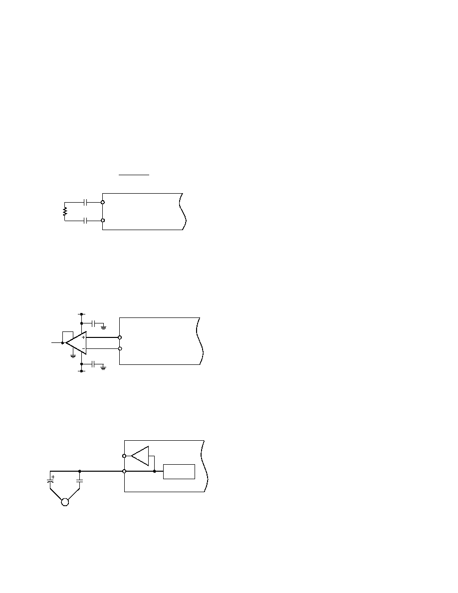
REV. 0
20
ADSP-21msp58/59
APPLICATION EXAMPLES
The ADSP-21msp58/59 is ideal for speech processing applica-
tions where high performance for analog and digital circuitry is
required, but board space is severely limited. The cellular radio
handset is one application. Here the ADSP-21msp58/59 can
digitize the speech, then perform compression algorithms that
sufficiently reduce the bit rate for transmission in a limited radio
bandwidth.
DEFINITION OF SPECIFICATIONS
Absolute Gain
Absolute gain is a measure of converter gain for a known signal.
Absolute gain is measured with a 1.0 kHz sine wave at 0 dBm0.
The absolute gain specification is used as a reference for the
gain tracking error specification.
Gain Tracking Error
Gain tracking error measures changes in converter output for
different signal levels relative to an absolute signal level. The
absolute signal level is 1.0 kHz at 0 dBm0. Gain tracking error
at 0 dBm0 is 0 dB by definition.
SNR + THD
Signal-to-noise ratio plus total harmonic distortion is defined to
be the ratio of the rms value of the measured input signal to the
rms sum of all other spectral components in the frequency range
300 Hz3400 Hz, including harmonics but excluding dc.
Intermodulation Distortion
With inputs consisting of sine waves at two frequencies, fa and
fb, any active device with nonlinearities will create distortion
products at sum and difference frequencies of mfa
±
nfb where
m, n = 0, 1, 2, 3, etc. Intermodulation terms are those which
neither m nor n are equal to zero. The second order terms in-
clude (fa + fb) and (fa fb), while the third order terms include
(2fa + fb), (2fa fb), (fa + 2fb), and (fa 2fb).
Idle Channel Noise
Idle channel noise is defined as the total signal energy measured
at the output of the device when the input is grounded (mea-
sured in the frequency range 300 Hz3400 Hz).
Crosstalk
Crosstalk is defined as the ratio of the rms value of a full-scale
signal appearing on one channel to the rms value of the same
signal that couples onto the adjacent channel. Crosstalk is ex-
pressed in dB.
Power Supply Rejection
Power supply rejection measures the susceptibility of a device to
a signal on the power supply. Power supply rejection is mea-
sured by modulating a signal on the power supply and measur-
ing the signal at the output (relative to 0 dB). Power supply
rejection is defined as the ratio of the rms value of the modula-
tion signal to the rms value of the same signal in the ADC/DAC
channel.
Group Delay
Group delay is defined as the derivative of radian phase with re-
spect to radian frequency,
(
)/
. Group delay is a measure
of the average delay of a system as a function of frequency. A
linear system with a constant group delay has a linear phase re-
sponse. The deviation of group delay away from a constant indi-
cates the degree of nonlinear phase response of the system.
Analog Signal Output
The differential analog output (VOUT
P
, VOUT
N
) is produced
by an on-chip differential amplifier which is part of the processor's
analog interface. The differential amplifier will meet dynamic
specifications for loads greater than 2 k
(R
L
2 k
) and has a
maximum differential output voltage swing of
±
3.156 V peak-to-
peak (3.17 dBm0). The DAC will drive loads smaller than 2 k
,
but with degraded dynamic performance. The differential out-
put can be ac-coupled directly to a load or dc-coupled to an ex-
ternal amplifier.
Figure 11 shows a simple circuit providing a differential output
with ac coupling. The capacitor of this circuit (C
OUT
) is op-
tional; if used, its value can be chosen as follows:
C
OUT
=
1
(60
) R
L
VOUT
P
VOUT
N
C
OUT
C
OUT
R
L
ADSP-21msp58/59
Figure 11. Example Circuit for Differential Output with
AC Coupling
The VOUT
P
and VOUT
N
outputs must be used as differential
outputs (do not use either as a single-ended output). Figure 12
shows an example circuit which can be used to convert the dif-
ferential output to a single-ended output. The circuit uses a dif-
ferential-to-single-ended amplifier, the Analog Devices SSM2141.
ADSP-21msp58/59
5
7
4
1
GND
A
0.1µF
GND
A
SSM2141
12V
0.1µF
GND
A
+12V
VOUT
P
VOUT
N
V
OUT
Figure 12. Example Circuit for Single-Ended Output
Voltage Reference Filter Capacitance
Figure 13 shows the recommended reference filter capacitor
connections. The capacitor grounds should be connected to the
same star ground point shown in Figure 10.
VOLTAGE
REFERENCE
0.1µF
STAR
GROUND
ADSP-21msp58/59
10µF
REF_FILTER
V
REF
BUF
Figure 13. Voltage Reference Filter Capacitor

ADSP-21msp58/59SPECIFICATIONS
RECOMMENDED OPERATING CONDITIONS
B Grade
Parameter
Min
Max
Unit
V
DD
Supply Voltage
4.50
5.50
V
T
AMB
Ambient Operating Temperature
40
+85
°
C
See "Environmental Conditions" for information on thermal specifications.
ELECTRICAL CHARACTERISTICS
Parameter
Test Conditions
Min
Max
Unit
V
IH
Hi-Level Input Voltage
1, 2
@ V
DD
= max
2.0
V
V
IH
Hi-Level CLKIN Voltage
@ V
DD
= max
2.2
V
V
IL
Lo-Level Input Voltage
1, 3
@ V
DD
= min
0.8
V
V
OH
Hi-Level Output Voltage
1, 4, 5
@ V
DD
= min,
I
OH
= 0.5 mA
2.4
V
@ V
DD
= min,
I
OH
= 100
µ
A
6
V
DD
0.3
V
V
OL
Lo-Level Output Voltage
1, 4, 5
@ V
DD
= min,
I
OL
= 2 mA
0.4
V
I
IH
Hi-Level Input Current
3
@ V
DD
= max,
V
IN
= V
DD
max
10
µ
A
I
IL
Lo-Level Input Current
3
@ V
DD
= max,
V
IN
= 0 V
10
µ
A
I
OZH
Tristate Leakage Current
7
@ V
DD
= max,
V
IN
= V
DD
max
8
10
µ
A
I
OZL
Tristate Leakage Current
7
@ V
DD
= max,
V
IN
= 0 V
8
10
µ
A
I
DD
Digital Supply Current (Idle)
6, 9
@ V
DD
= max,
Codec Inactive
18
mA
I
DD
Digital Supply Current (Dynamic)
9, 10
@ V
DD
= max,
V
CC
= max
92
mA
I
DD
Digital Supply Current (Powerdown)
9
@ V
DD
= max, See
ADSP-2100 Family User's
Manual, Chapter 9
100
µ
A
I
CC
Analog Supply Current (Dynamic)
9
Codec Active
18
mA
C
I
Input Pin Capacitance
3, 11, 12
@ V
IN
= 2.5 V,
f
IN
= 1.0 MHz,
T
AMB
= 25
°
C
8
pF
C
O
Output Pin Capacitance
7, 11, 12
@ V
IN
= 2.5 V,
f
IN
= 1.0 MHz,
T
AMB
= 25
°
C
8
pF
NOTES
1
Bidirectional pins: D0-D23, RFS0, RFS1, SCLK0, SCLK1, TFS0, TFS1, HD0-HD7/HAD0-HAD7.
2
Input only pins: RESET, IRQ2, BR, MMAP, DR0, DR1, HSEL, HSIZE, BMODE, HMD0, HMD1, HRD/HWR, HWR/HDS, PWD, HA2/ALE, HA1-0.
3
Input only pins: CLKIN, RESET, IRQ2, BR, MMAP, DR0, DR1, HSEL, HSIZE, BMODE, HMD0, HMD1, HRD/HWR, HWR/HDS, PWD, HA2/ALE, HA1-0.
4
Output pins: BG, PMS, DMS, BMS, RD, WR, A0-A13, DT0, DT1, CLKOUT, HACK, FL0.
5
Although specified for TTL outputs, all ADSP-21msp58/59 outputs are CMOS-compatible and will drive to V
DD
and GND, assuming no dc loads.
6
Idle refers to ADSP-21msp58/59 state of operation during IDLE instruction. Deasserted pins are driven to either V
DD
or GND. Refer to chart in back for lower
IDLE currents.
7
Three-statable pins: A0-A13, D0-D23, PMS, DMS, BMS, RD, WR, DT0, DT1, SCLK0, SCLK1, TFS0, TFS1, RFS0, RSF1, HD0-HD7/HAD0-HAD7.
8
0 V on BR, CLKIN Active (to force three-state condition).
9
Current reflects the digital portion of device operating with no output loads and a 2 k
load on the analog output (VOUT
P
, VOUT
N
).
10
t
CK
= 76.92 ns, CODEC active, 80% execution type 1 instructions, with random data. For typical figures for digital and analog supply currents, refer to "Power
Dissipation" section.
11
Guaranteed but not tested.
12
Output pin capacitance is the capacitive load for any three-stated output pin.
Specifications subject to change without notice.
21
REV. 0
ADSP-21msp58/59

REV. 0
22
ADSP-21msp58/59
MEMORY REQUIREMENTS
This chart links common memory device specification
names and ADSP-21msp58/59 timing parameters for your
convenience.
Common
Parameter
Memory Device
Name
Function
Specification Name
t
ASW
A0-A13, DMS, PMS
Address Setup to
Setup before WR Low
Write Start
t
AW
A0-A13, DMS, PMS Setup
Address Setup
before WR Deasserted
to Write End
t
WRA
A0-A13, DMS, PMS
Address Hold Time
Hold after WR Deasserted
t
DW
Data Setup before WR High Data Setup Time
t
DH
Data Hold after WR High
Data Hold Time
t
RDD
RD
Low to Data Valid
OE
to Data Valid
t
AA
A0-A13, DMS, PMS,
Address Access Time
BMS
to Data Valid
ESD SENSITIVITY
The ADSP-21msp58/59 is an ESD (electrostatic discharge) sensitive device. Electrostatic charges
readily accumulate on the human body and equipment and can discharge without detection.
Permanent damage may occur to devices subjected to high energy electrostatic discharges.
The ADSP-21msp58/59 features proprietary ESD protection circuitry to dissipate high energy
discharges (Human Body Model).
Proper ESD precautions are recommended to avoid performance degradation or loss of function-
ality. Unused devices must be stored in conductive foam or shunts, and the foam should be
discharged to the destination before devices are removed.
GENERAL NOTES
Use the exact timing information given. Do not attempt to de-
rive parameters from the addition or subtraction of others. While
addition or subtraction would yield meaningful results for an in-
dividual device, the values given in this data sheet reflect statisti-
cal variations and worst cases. Consequently, you cannot
meaningfully add up parameters to derive longer times.
TIMING NOTES
Switching characteristics specify how the processor changes its
signals. You have no control over this timing; it is dependent on
the internal design. Timing requirements apply to signals that
are controlled outside the processor, such as the data input for a
read operation.
Timing requirements guarantee that the processor operates cor-
rectly with another device. Switching characteristics tell you
what the device will do under a given circumstance. Also, use the
switching characteristics to ensure any timing requirement of a
device connected to the processor (such as memory) is satisfied.
TIMING PARAMETERS
WARNING!
ESD SENSITIVE DEVICE
ABSOLUTE MAXIMUM RATINGS
*
Supply Voltage . . . . . . . . . . . . . . . . . . . . . . . . . . 0.3 V to +7 V
Input Voltage . . . . . . . . . . . . . . . . . . . . . 0.3 V to V
DD
+ 0.3 V
Output Voltage Swing . . . . . . . . . . . . . . 0.3 V to V
DD
+ 0.3 V
Operating Temperature Range (Ambient) . . . . 40
°
C to +85
°
C
Storage Temperature Range . . . . . . . . . . . . . 65
°
C to +150
°
C
Lead Temperature (5 sec) . . . . . . . . . . . . . . . . . . . . . . +280
°
C
*
Stresses above those listed under "Absolute Maximum Ratings" may cause
permanent damage to the device. These are stress ratings only, and functional
operation of the device at these or any other conditions above those indicated in the
operational sections of this specification is not implied. Exposure to absolute
maximum rating conditions for extended periods may affect device reliability.
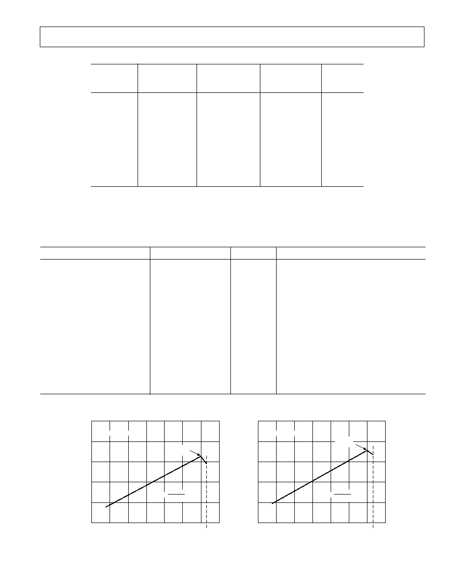
ADSP-21msp58/59
REV. 0
23
FREQUENCY RESPONSE
ADC
ADC
DAC
DAC
Frequency
Max
Min
Max
Min
(Hz)
(dB)
(dB)
(dB)
(dB)
0+
60.00
N/A
60.00
N/A
75
25.00
N/A
25.00
N/A
150
+0.266
0.134
+0.015
0.185
300
+0.272
0.128
+0.030
0.170
1000
+0.000
+0.000
+0.000
+0.000
2000
+0.050
0.350
+0.050
0.200
3000
0.200
0.600
0.050
0.300
3400
0.300
0.700
0.090
0.340
3700
0.375
0.775
0.120
0.370
3850
25.00
N/A
25.00
N/A
4000
60.00
N/A
60.00
N/A
NOTES
All specifications relative to absolute gain @ 1.0 kHz.
ADC and DAC high-pass filters inserted.
ADC specifications do not include RC filter attenuation and assumes an ac coupled input (see "Analog Test Conditions"
for RC filter details).
NOISE & DISTORTION
Parameter
Min
Max
Unit
Test Condition
ADC Intermodulation Distortion
60
dB
m, n = 1 and 2; f
a
= 984; f
b
= 1047
DAC Intermodulation Distortion
70
dB
m, n = 1 and 2; f
a
= 984; f
b
= 1047
ADC Idle Channel Noise
65
dBm0
DAC Idle Channel Noise
72
dBm0
ADC Crosstalk
1
65
dB
ADC input signal level: 1.0 kHz, 0 dBm0
DAC input at idle.
DAC Crosstalk
1
65
dB
ADC input signal level: analog ground
DAC output signal level: 1.0 kHz, 0 dBm0
ADC Power Supply Rejection
1
55
dB
Input signal level at V
CC
and V
DD
pins:
1.0 kHz, 100 mV p-p sine wave
DAC Power Supply Rejection
1
55
dB
Input signal level at V
CC
and V
DD
pins:
1.0 kHz, 100 mV p-p sine wave
ADC Group Delay
1
1
ms
300 Hz3000 Hz
DAC Group Delay
1
1
ms
300 Hz3000 Hz
ADC SNR and THD
65
dB
1.0 kHz, 0 dBm0
DAC SNR and THD
72
dB
1.0 kHz, 0 dBm0
NOTE
1
Guaranteed but not tested.
V
IN
dBm0
100
80
0
SNR + THD dB
60
10
50
40
30
20
10
0
60
40
20
DAC SNR + THD
3.17
PEAK @
72dB
SLOPE =
20dB
20dBm0
V
IN
dBm0
100
80
0
SNR + THD dB
60
10
50
40
30
20
10
0
60
40
20
ADC SNR + THD
3.17
PEAK @
65dB
SLOPE =
20dB
20dBm0
Figure 14. SNR + THD vs. V
IN

REV. 0
24
ADSP-21msp58/59
ANALOG INTERFACE ELECTRICAL CHARACTERISTICS
Symbol
Parameter
Min
Typ
Max
Unit
ADC
R
I
Input Resistance
1, 2
at VIN
NORM
, VIN
AUX
200
k
VIN
MAX
Maximum Input Range
1, 3
3.156
V p-p
DAC:
R
O
Output Resistance
1, 4
2.5
V
OOFF
Output DC Offset
5
400
400
mV
V
O
Maximum Voltage Output Swing (p-p) Across R
L
Single-Ended
1
3.156
V
Differential
1
6.312
V
R
L
Load Resistance
1, 4
2
k
Reference Buffer:
Voltage Reference (V
REF
)
2.25
2.75
V
Output Impedence
1
250
Capacitive Load
1
10
nf
PSRR
1
55
dB
NOTES
Test conditions for all analog interface tests: ADC PGA bypassed, DAC PGA set to 0 dB gain, with 2 k
load on analog output (VOUT
P
, VOUT
N
), V
CC
= 5.0 V.
1
Guaranteed but not tested.
2
Varies with PGA setting.
3
At input to sigma-delta modulator of ADC.
4
At VOUT
P
, VOUT
N
.
5
Between VOUT
P
and VOUT
N
.
GAIN
Parameter
Min
Typ
Max
Unit
Test Conditions
ADC Absolute Gain
0.7
0
0.7
dBm0
1.0 kHz, 0 dBm0
ADC Gain Tracking Error
0.1
0
0.1
dBm0
1.0 kHz, +3 to 50 dBm0
ADC PGA Relative Gain
0.6
0
0.6
dBm0
1.0 kHz
DAC Absolute Gain
0.75
0
0.75
dBm0
1.0 kHz, 0 dBm0
DAC Gain Tracking Error
0.1
0
0.1
dBm0
1.0 kHz, +3 to 50 dBm0
DAC PGA Relative Gain
0.6
0
0.6
dBm0
1.0 kHz
ADSP-21msp58/59
REV. 0
25
Parameter
Min
Max
Unit
Clock Signals
t
CK
is defined as 0.5 t
CKI.
The ADSP-21msp58/59 uses
an input clock with a quency equal to half the instruction
rate; a 13 MHz input clock (which is equivalent to 76.92 ns)
yields a 38.46 ns processor cycle (equivalent to 26 MHz).
t
CK
values within the range of 0.5 t
CKI
period should be
substituted for all relevant timing parameters to obtain
specification value. Example: t
CKH
= 0.5t
CK
7 ns
= 0.5 (38.46 ns) 7 ns = 12.23 ns.
Timing Requirement:
t
CKI
CLKIN Period
76.92
125
ns
t
CKIL
CLKIN Width Low
20
ns
t
CKIH
CLKIN Width High
20
ns
Switching Characteristic:
t
CKL
CLKOUT Width Low
0.5t
CK
7
ns
t
CKH
CLKOUT Width High
0.5t
CK
7
ns
t
CKOH
CLKIN High to CLKOUT High
0
20
ns
Control Signals
Timing Requirement:
t
RSP
RESET
Width Low
5t
CK
1
ns
NOTES
1
Applies after power-up sequence is complete. Internal phase lock loop requires no more than 2000 CLKIN cycles assuming stable CLKIN (not including
crystal oscillator start-up time).
CLKIN
t
CKIL
t
CKIH
t
CKI
t
CKOH
t
CKH
t
CKL
CLKOUT
Figure 15. Clock Signals
REV. 0
26
ADSP-21msp58/59
Parameter
Min
Max
Unit
Interrupts and Flags
Timing Requirement:
t
IFS
IRQx
or FI Setup before CLKOUT Low
1, 2, 3
0.25t
CK
+ 15
ns
t
IFH
IRQx
or FI Hold after CLKOUT High
1, 2, 3
0.25t
CK
ns
Switching Characteristics:
t
FOH
Flag Output Hold after CLKOUT Low
4
0.5t
CK
7
ns
t
FOD
Flag Output Delay from CLKOUT Low
4
0.5t
CK
+ 5
ns
NOTES
1
If IRQx and FI inputs meet t
IFS
and t
IFH
setup/hold requirements, they will be recognized during the current clock cycle; otherwise the signals will be recognized on
the following cycle. (Refer to "Interrupt Controller Operation" in the Program Control chapter of the User's Manual for further information on interrupt servicing.)
2
Edge-sensitive interrupts require pulse widths greater than 10 ns; level-sensitive interrupts must be held low until serviced.
3
IRQx
= IRQ0, IRQ1, and IRQ2.
4
Flag Output = FL0 and FO.
FLAG
OUTPUTS
t
FOD
t
I FS
t
I FH
CLKOUT
t
FOH
IRQ
FI
x
Figure 16. Interrupts and Flags
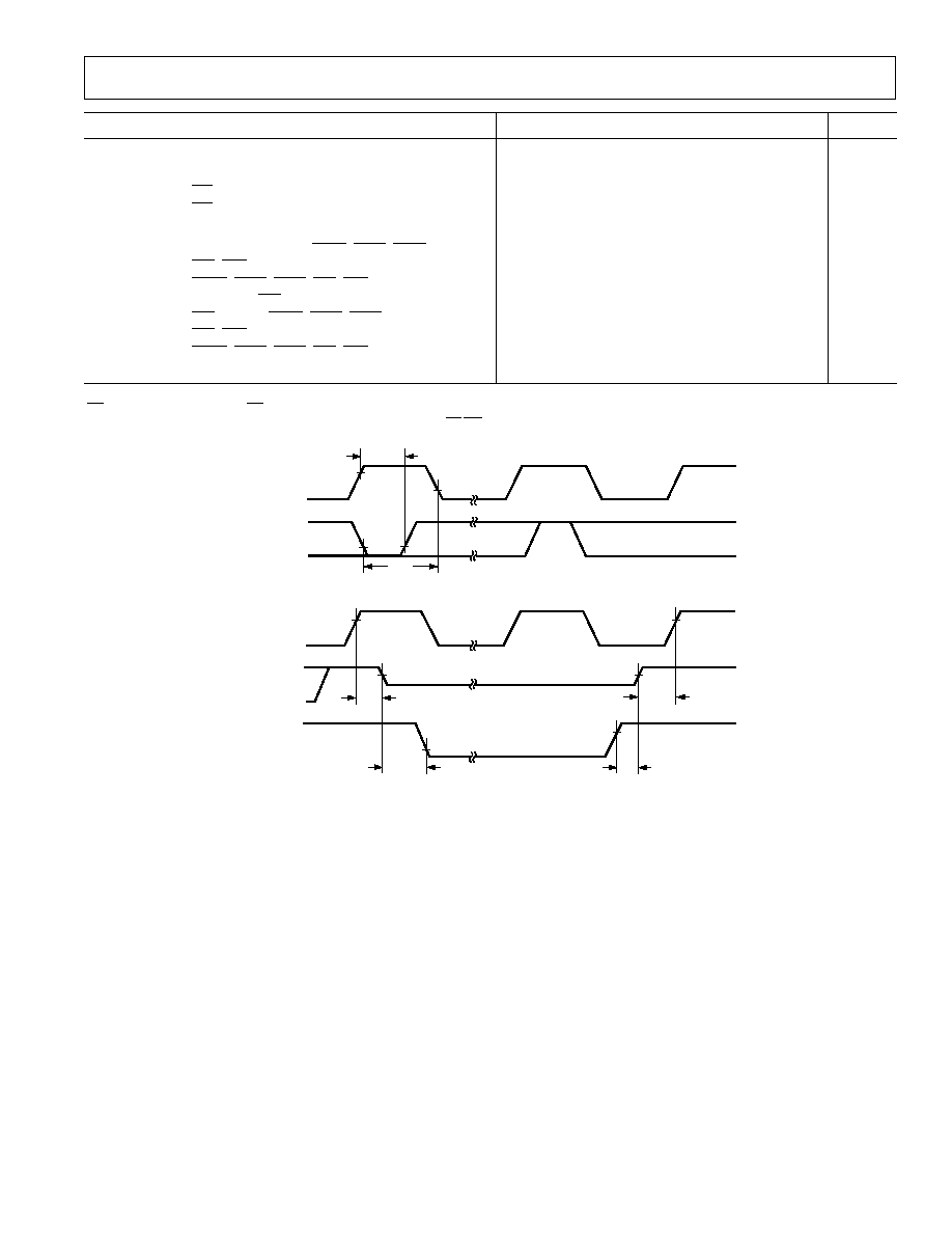
ADSP-21msp58/59
REV. 0
27
Parameter
Min
Max
Unit
Bus Request/Grant
Timing Requirement:
t
BH
BR
Hold after CLKOUT High
1
0.25t
CK
+ 2
ns
t
BS
BR
Setup before CLKOUT Low
1
0.25t
CK
+ 17
ns
Switching Characteristic:
t
SD
CLKOUT High to DMS, PMS, BMS,
0.25t
CK
+ 10
ns
RD
, WR Disable
t
SDB
DMS
, PMS, BMS, RD, WR
Disable to BG Low
0
ns
t
SE
BG
High to DMS, PMS, BMS,
RD
, WR Enable
0
ns
t
SEC
DMS
, PMS, BMS, RD, WR
Enable to CLKOUT High
0.25t
CK
7
ns
NOTES
1
BR
is an asynchronous signal. If BR meets the setup/hold requirements, it will be recognized during the current clock cycle; otherwise the signal will be recognized
on the following cycle. Refer to the ADSP-2100 Family User's Manual for BR/BG cycle relationships.
CLKOUT
t
BS
t
BH
BR
CLKOUT
t
SD
t
SDB
t
S E C
t
SE
PMS
,
DMS
,
BMS
,
RD
,
WR
BG
Figure 17. Bus RequestBus Grant
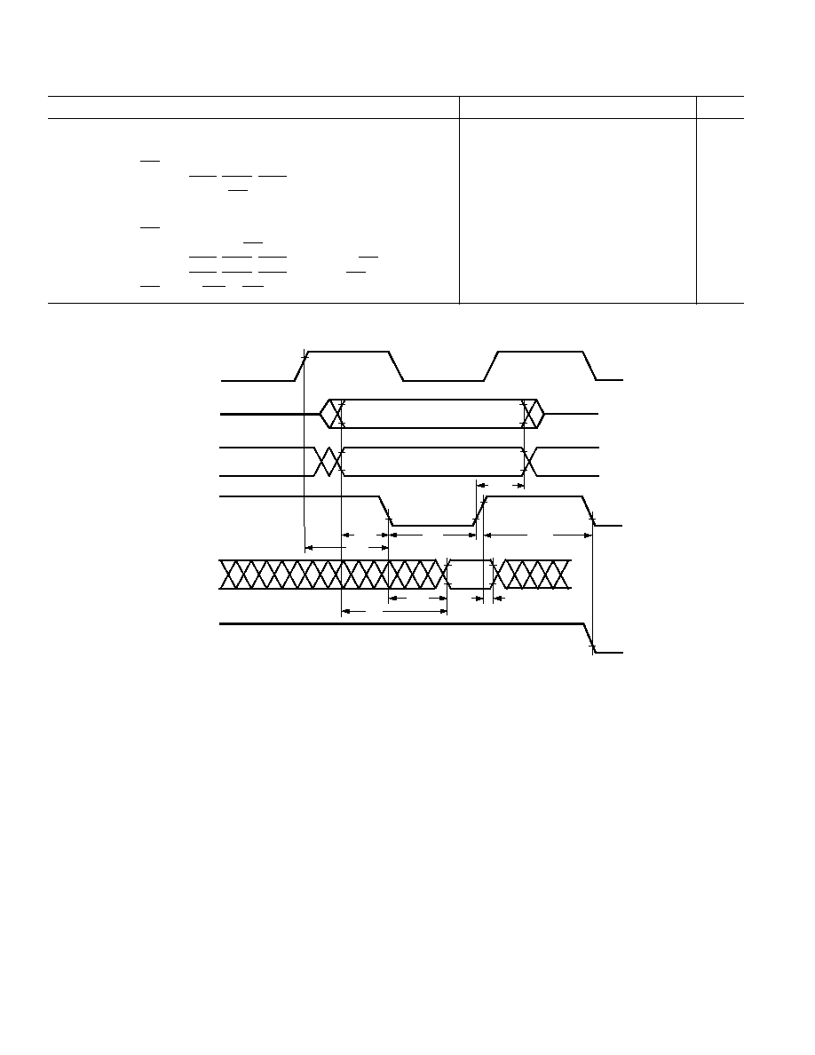
REV. 0
28
ADSP-21msp58/59
Parameter
Min
Max
Unit
Memory Read
Timing Requirement:
t
RDD
RD
Low to Data Valid
0.5t
CK
11 + w
ns
t
AA
A0-A13, PMS, DMS, BMS to Data Valid
0.75t
CK
12 + w
ns
t
RDH
Data Hold from RD High
0
ns
Switching Characteristic:
t
RP
RD
Pulse Width
0.5t
CK
5 + w
ns
t
CRD
CLKOUT High to RD Low
0.25t
CK
5
0.25t
CK
+ 7
ns
t
ASR
A0-A13, PMS, DMS, BMS Setup before RD Low
0.25t
CK
6
ns
t
RDA
A0-A13, PMS, DMS, BMS Hold after RD Deasserted
0.25t
CK
3
ns
t
RWR
RD
High to RD or WR Low
0.5t
CK
5
NOTE
w = wait states
×
t
CK
.
CLKOUT
t
R P
WR
DMS
,
PMS
,
BMS
t
RDA
t
ASR
t
CRD
t
R W R
t
RDH
t
ROD
t
AA
A0 A13
RD
D
Figure 18. Memory Read
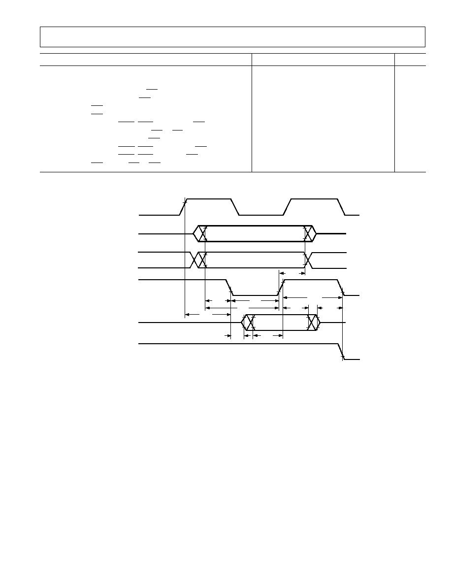
ADSP-21msp58/59
REV. 0
29
Parameter
Min
Max
Unit
Memory Write
Switching Characteristic:
t
DW
Data Setup before WR High
0.5t
CK
7 + w
ns
t
DH
Data Hold after WR High
0.25t
CK
2
ns
t
WP
WR
Pulse Width
0.5t
CK
5 + w
ns
t
WDE
WR
Low to Data Enabled
0
ns
t
ASW
A0-A13, DMS, PMS Setup before WR Low
0.25t
CK
6
ns
t
DDR
Data Disable before WR or RD Low
0.25t
CK
6
ns
t
CWR
CLKOUT High to WR Low
0.25t
CK
5
0.25t
CK
+ 7
ns
t
AW
A0-A13, DMS, PMS, Setup before WR Deasserted
0.75t
CK
9 + w
ns
t
WRA
A0-A13, DMS, PMS Hold after WR Deasserted
0.25t
CK
3
ns
t
WWR
WR
High to RD or WR Low
0.5t
CK
5
ns
NOTE
w = wait states
×
t
CK.
CLKOUT
t
W P
DMS
,
PMS
t
W RA
t
ASW
t
CWR
t
W W R
t
WDE
A0 A13
WR
D
t
A W
t
D H
t
D D R
t
D W
RD
Figure 19. Memory Write
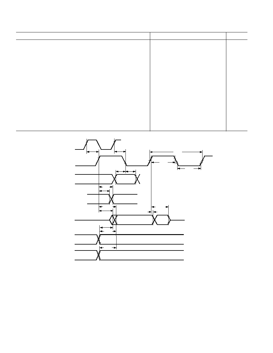
REV. 0
30
ADSP-21msp58/59
Parameter
Min
Max
Unit
Serial Ports
Timing Requirement:
t
SCK
SCLK Period
50
ns
t
SCS
DR/TFS/RFS Setup before SCLK Low
4
ns
t
SCH
DR/TFS/RFS Hold after SCLK Low
7
ns
t
SCP
SCLK
in
Width
20
ns
Switching Characteristic:
t
CC
CLKOUT High to SCLK
out
0.25t
CK
0.25t
CK
+ 10
ns
t
SCDE
SCLK High to DT Enable
0
ns
t
SCDV
SCLK High to DT Valid
15
ns
t
RH
TFS/RFS
out
Hold after SCLK High
0
ns
t
RD
TFS/RFS
out
Delay from SCLK High
15
ns
t
SCDH
DT Hold after SCLK High
0
ns
t
TDE
TFS(Alt) to DT Enable
0
ns
t
TDV
TFS(Alt) to DT Valid
14
ns
t
SCDD
SCLK High to DT Disable
15
ns
t
RDV
RFS (Multichannel, Frame Delay Zero) to DT Valid
15
ns
CLKOUT
t
R H
t
R D
t
C C
t
C C
t
S C H
t
S C S
t
S C P
t
S C P
t
S C K
t
S C D E
t
S C D V
t
S C D H
t
S C D D
t
T D V
t
T D E
t
R D V
SCLK
DR
RFS
IN
TFS
IN
RFS
OUT
TFS
OUT
DT
TFS
alternate
frame mode
RFS
multichannel
mode, frame
delay 0 (MFD = 0)
Figure 20. Serial Ports
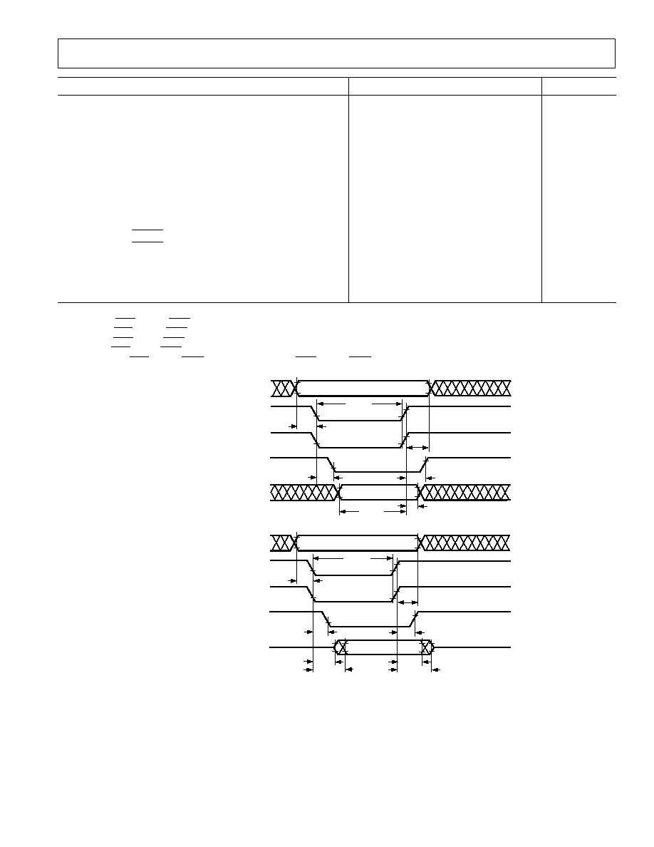
ADSP-21msp58/59
REV. 0
31
Parameter
Min
Max
Unit
Host Interface Port
Separate Data and Address (HMD1 = 0)
Read Strobe and Write Strobe (HMD0 = 0)
Timing Requirement:
t
HSU
HA2-0 Setup before Start of Write or Read
1, 2
5
ns
t
HDSU
Data Setup before End of Write
3
5
ns
t
HWDH
Data Hold after End of Write
3
3
ns
t
HH
HA2-0 Hold after End of Write or Read
3, 4
3
ns
t
HRWP
Read or Write Pulse Width
5
20
ns
Switching Characteristic:
t
HSHK
HACK
Low after Start of Write or Read
1, 2
0
15
ns
t
HKH
HACK
Hold after End of Write or Read
3, 4
0
15
ns
t
HDE
Data Enabled after Start of Read
2
0
ns
t
HDD
Data Valid after Start of Read
2
18
ns
t
HRDH
Data Hold after End of Read
4
0
ns
t
HRDD
Data Disabled after End of Read
4
7
ns
NOTES
1
Start of Write = HWR Low and HSEL Low.
2
Start of Read = HRD Low and HSEL Low.
3
End of Write = HWR High or HSEL High.
4
End of Read = HRD High or HSEL High.
5
Read Pulse Width = HRD Low and HSEL Low, Write Pulse Width = HWR Low and HSEL Low.
HA20
t
H K H
t
H R W P
t
H H
ADDRESS
t
H S U
DATA
t
H S H K
t
H W D H
t
H D S U
HSEL
HWR
HACK
HOST WRITE CYCLE
HD70
HA20
t
H K H
t
H R W P
t
H H
ADDRESS
t
H S U
DATA
t
H S H K
t
H R D H
t
HRDD
HSEL
HRD
HACK
HOST READ CYCLE
HD70
t
H D E
t
H D D
Figure 21. Host Interface Port (HMD1 = 0, HMD0 = 0)
REV. 0
32
ADSP-21msp58/59
Parameter
Min
Max
Unit
Host Interface Port
Separate Data and Address (HMD1 = 0)
Read Strobe and Write Strobe (HMD0 = 1)
Timing Requirement:
t
HSU
HA2-0, HRW Setup before Start of Write or Read
1
5
ns
t
HDSU
Data Setup before End of Write
2
5
ns
t
HWDH
Data Hold after End of Write
2
3
ns
t
HH
HA2-0, HRW Hold after End of Write or Read
2
3
ns
t
HRWP
Read or Write Pulse Width
3
20
ns
Switching Characteristic:
t
HSHK
HACK
Low after Start of Write or Read
1
0
15
ns
t
HKH
HACK
Hold after End of Write or Read
2
0
15
ns
t
HDE
Data Enabled after Start of Read
1
0
ns
t
HDD
Data Valid after Start of Read
1
18
ns
t
HRDH
Data Hold after End of Read
2
0
ns
t
HRDD
Data Disabled after End of Read
2
7
ns
NOTES
1
Start of Write or Read = HDS Low and HSEL Low.
2
End of Write or Read = HDS High and HSEL High.
3
Read or Write Pulse Width = HDS Low and HSEL Low.
HA20
t
H K H
t
H R W P
t
H H
ADDRESS
t
H S U
t
H S H K
HSEL
HACK
HOST READ CYCLE
HD70
HDS
HRW
DATA
t
H R D H
t
HRDD
t
H D E
t
H D D
HA20
t
H K H
t
H R W P
t
H H
ADDRESS
t
H S U
DATA
t
H S H K
t
H W D H
t
H D S U
HSEL
HACK
HOST WRITE CYCLE
HD70
HDS
HRW
Figure 22. Host Interface Port (HMD1 = 0, HMD0 =1)
ADSP-21msp58/59
REV. 0
33
Parameter
Min
Max
Unit
Host Interface Port
Multiplexed Data and Address (HMD1 = 1)
Read Strobe and Write Strobe (HMD0 = 0)
Timing Requirement:
t
HALP
ALE Pulse Width
10
ns
t
HASU
HAD15-0 Address Setup, before ALE Low
5
ns
t
HAH
HAD15-0 Address Hold after ALE Low
2
ns
t
HALS
Start of Write or Read after ALE Low
1, 2
10
ns
t
HDSU
HAD15-0 Data Setup before End of Write
3
5
ns
t
HWDH
HAD15-0 Data Hold after End of Write
3
3
ns
t
HRWP
Read or Write Pulse Width
5
20
ns
Switching Characteristic:
t
HSHK
HACK
Low after Start of Write or Read
1, 2
0
15
ns
t
HKH
HACK
Hold after End of Write or Read
3, 4
0
15
ns
t
HDE
HAD15-0 Data Enabled after Start of Read
2
0
ns
t
HDD
HAD15-0 Data Valid after Start of Read
2
18
ns
t
HRDH
HAD15-0 Data Hold after End of Read
0
ns
t
HRDD
HAD15-0 Data Disabled after End of Read
4
7
ns
NOTES
1
Start of Write = HWR Low and HSEL Low.
2
Start of Read = HRD Low and HSEL Low.
3
End of Write = HWR High or HSEL High.
4
End of Read = HRD High or HSEL High.
5
Read Pulse Width = HRD Low and HSEL Low, Write Pulse Width = HWR Low and HSEL Low.
t
H K H
ALE
t
H R W P
ADDRESS
t
H A L P
DATA
t
H S H K
t
H W D H
t
H D S U
HSEL
HACK
HOST WRITE CYCLE
HAD70
HWR
t
H A L S
t
H A S U
t
H A H
t
H K H
ALE
t
H R W P
ADDRESS
t
H A L P
DATA
t
HSHK
t
HRDH
t
HDE
HSEL
HACK
HOST READ CYCLE
HAD70
HRD
t
H A L S
t
H A S U
t
H A H
t
HRDD
t
HDD
Figure 23. Host Interface Port (HMD1 = 1, HMD0 = 0)
REV. 0
34
ADSP-21msp58/59
Parameter
Min
Max
Unit
Host Interface Port
Multiplexed Data and Address (HMD1 = 1)
Read Strobe and Write Strobe (HMD0 = 1)
Timing Requirement:
t
HALP
ALE Pulse Width
10
ns
t
HASU
HAD15-0 Address Setup before ALE Low
5
ns
t
HAH
HAD15-0 Address Hold after ALE Low
2
ns
t
HALS
Start of Write or Read after ALE Low
1
10
ns
t
HSU
HRW Setup before Start of Write or Read
1
5
ns
t
HDSU
HAD15-0 Data Setup before End of Write
2
5
ns
t
HWDH
HAD15-0 Data Hold after End of Write
2
3
ns
t
HH
HRW Hold after End of Write or Read
2
3
ns
t
HRWP
Read or Write Pulse Width
3
20
ns
Switching Characteristic:
t
HSHK
HACK
Low after Start of Write or Read
1
0
15
ns
t
HKH
HACK
Hold after End of Write or Read
2
0
15
ns
t
HDE
HAD15-0 Data Enabled after Start of Read
1
0
ns
t
HDD
HAD15-0 Data Valid after Start of Read
1
18
ns
t
HRDH
HAD15-0 Data Hold after End of Read
2
0
ns
t
HRDD
HAD15-0 Data Disabled after End of Read
2
7
ns
NOTES
1
Start of Write or Read = HDS Low and HSEL Low.
2
End of Write or Read = HDS High and HSEL High.
3
Read or Write Pulse Width = HDS Low and HSEL Low.
t
H K H
ALE
t
H R W P
ADDRESS
t
H A L P
DATA
t
H S U
t
HWDH
t
HDSU
HSEL
HACK
HOST WRITE CYCLE
HAD70
HRW
t
H A L S
t
HASU
t
HAH
t
H H
t
H S H K
HDS
t
H H
ALE
t
H R W P
ADDRESS
t
H A L P
DATA
t
HSHK
t
HKH
t
HDE
HSEL
HACK
HOST READ CYCLE
HAD70
HRW
t
H A L S
t
H A S U
t
H A H
t
HRDD
t
HDD
t
H S U
t
HRDH
HDS
Figure 24. Host Interface Port (HMD1 = 1, HMD0 = 1)
ADSP-21msp58/59
REV. 0
35
ENVIRONMENTAL CONDITIONS
Ambient Temperature Rating:
T
AMB
= T
CASE
(PD
×
CA
)
T
CASE
= Case Temperature in
°
C
PD = Power Dissipation in W
CA
= Thermal Resistance (Case-to-Ambient)
JA
= Thermal Resistance (Junction-to-Ambient)
JC
= Thermal Resistance (Junction-to-Case)
Package
JA
JC
CA
TQFP
50
°
C/W
2
°
C/W
48
°
C/W
POWER DISSIPATION
To determine total power dissipation in a specific application,
the following equation should be applied for each output:
C
×
V
DD
2
×
f
C = load capacitance, f = output switching frequency.
Example:
In an application where external data memory is used and no
other outputs are active, power dissipation is calculated as
follows:
Assumptions:
·
External data memory is accessed every cycle with 50% of the
address pins switching.
·
External data memory writes occur every other cycle with
50% of the data pins switching.
·
Each address and data pin has a 10 pF total load at the pin.
·
The application operates at V
DD
= 5.0 V and t
CK
= 76.92 ns.
Total Power Dissipation = P
INT
+ (C
×
V
DD
2
×
f )
P
INT
= internal power dissipation from Power vs. Frequency
graph (Figure 25).
(C
×
V
DD
2
×
f ) is calculated for each output:
# of
Pins
×
C
×
V
DD
2
×
f
Address, DMS
8
×
10 pF
×
5
2
V
×
26 MHz
=
52 mW
Data Output, WR 9
×
10 pF
×
5
2
V
×
13 MHz
=
30 mW
RD
1
×
10 pF
×
5
2
V
×
13 MHz
=
4 mW
CLKOUT
1
×
10 pF
×
5
2
V
×
26 MHz
=
6 mW
92 mW
Total power dissipation for this example is P
INT
+ 92 mW.
Typical Power Consumption
The typical power consumption can be calculated from the fol-
lowing data, taken at 5.0 V and +25
°
C. Dynamic V
DD
data was
taken while executing 80% type 1 multifunction instructions, on
random data.
Parameter
Typ
I
DD
Digital Supply Current (Idle, Codec Powered Up)
19 mA
I
DD
Digital Supply Current (Idle)
13 mA
I
DD
Digital Supply Current (Dynamic, Codec Powered Up) 83 mA
I
DD
Digital Supply Current (Dynamic)
78 mA
I
DD
Digital Supply Current (Powerdown)
10
µ
A
I
CC
Analog Supply Current (Dynamic)
15 mA
Analog Devices recommends that the ADSP-21msp58/59
is used with a 13 MHz input clock. Below this input clock
frequency, the codec performance changes and the performance
specifications cannot be guaranteed. The codec filter character-
istics, however, scale approximately linearly with frequency.
If the codec is disabled, then the processor can be used at any
allowed input frequency. The power consumption of the ADSP-
21msp58/59 at these frequencies is shown in Figure 25.
65mW
37mW
35mW
29mW
21mW
20mW
70
60
50
40
30
20
10
POWER,
IDLE n MODES
3
2
6
10
14
18
22
26
30
IDLEs @ 5.0V
CODEC INACTIVE
TYPICAL VALUES
IDLE (16)
IDLE (32)
IDLE (64)
IDLE (128)
1/t
CK
MHz
POWER (P
IDLE
N) mW
POWER, IDLE
2
110
100
90
80
70
60
50
40
30
2
6
10
14
18
22
26
30
1/t
CK
MHz
100mW
83mW
69mW
57mW
49mW
42mW
V
DD
= 5.5V
V
DD
= 4.5V
POWER (P
IDLE
) mW
IDLE 0
CODEC INACTIVE
MAX VALUES
V
DD
= 5.0V
POWER, INTERNAL
1
480mW
391mW
310mW
191mW
154mW
118mW
550
500
450
400
350
300
250
200
150
100
50
2
6
10
14
18
22
26
30
POWER (P
INT
) mW
V
DD
= 5.5V
V
DD
= 4.5V
1/t
CK
MHz
INTERNAL
(80% NOMINAL LOADING)
CODEC INACTIVE
MAX VALUES
550
500
450
400
350
300
250
200
150
100
50
V
DD
= 5.0V
1
2
3
VALID FOR ALL TEMPERATURE GRADES.
POWER REFLECTS DEVICE OPERATING WITH NO OUTPUT LOADS.
IDLE REFERS TO ADSP-21msp58/59 STATE OF OPERATION DURING EXECUTION OF
IDLE INSTRUCTION. DEASSERTED PINS ARE DRIVEN TO EITHER V
DD
OR GND.
POWER REFLECTS DEVICE OPERATING WITH CLKOUT DISABLED.
TYPICAL POWER DISSIPATION AT 5.0V V
DD
DURING EXECUTION OF
IDLE n
INSTRUCTION (CLOCK FREQUENCY REDUCTION). POWER REFLECTS DEVICE
OPERATING WITH CLKOUT DISABLED.
Figure 25. Power vs. Internal Processor Frequency
REV. 0
36
ADSP-21msp58/59
CAPACITIVE LOADING
Figures 26 and 27 show the capacitive loading characteristics of
the ADSP-21msp58/59.
C
L
pF
RISE TIME (0.4V 2.4V) ns
28
0
25
175
50
75
100
125
150
24
16
12
8
4
20
V
DD
= 4.5V
Figure 26. Typical Output Rise Time vs. Load Capacitance,
C
L
(at Maximum Ambient Operating Temperature)
C
L
pF
+14
4
+12
+6
+2
NOMINAL
2
+10
+8
+4
25
175
50
75
100
125
150
VALID OUTPUT DELAY OR HOLD ns
Figure 27. Typical Output Valid Delay or Hold vs. Load
Capacitance, C
L
(at Maximum Ambient Operating
Temperature)
TEST CONDITIONS
Digital
Figure 28 shows the voltage reference levels and Figure 29
shows the equivalent device loading for the ac measurements.
3.0V
1.5V
0.0V
2.0V
1.5V
0.8V
INPUT
OUTPUT
Figure 28. Voltage Reference Levels for AC Measure-
ments (Except Output Enable/Disable)
50pF
TO
OUTPUT
PIN
I
OH
I
OL
+1.5V
Figure 29. Equivalent Device Loading for AC Measure-
ments (Including All Fixtures)
Analog
Figure 30 shows the analog test conditions.
2200pF
NPO
1.0µF
VIN
NORM
2.2k
2200pF
NPO
1.0µF
VIN
AUX
2.2k
1.0µF
DECOUPLE
0.1µF
REF_CAP
10µF
Figure 30. Analog Test Conditions
ADSP-21msp58/59
REV. 0
37
Output Disable Time
Output pins are considered to be disabled when they have
stopped driving and started a transition from the measured out-
put high or low voltage to a high impedance state. The output
disable time (t
DIS
) is the difference of t
MEASURED
and t
DECAY
, as
shown in the Output Enable/Disable diagram. The time is the
interval from when a reference signal reaches a high or low volt-
age level to when the output voltages have changed by 0.5 V
from the measured output high or low voltage. The decay time,
t
DECAY
, is dependent on the capacitative load, C
L
, and the cur-
rent load, i
L
, on the output pin. It can be approximated by the
following equation:
t
DECAY
=
C
L
· 0.5V
i
L
from which
t
DIS
=
t
MEASURED
t
DECAY
is calculated. If multiple pins (such as the data bus) are dis-
abled, the measurement value is that of the last pin to stop
driving.
Output Enable Time
Output pins are considered to be enabled when that have made
a transition from a high-impedance state to when they start driv-
ing. The output enable time (t
ENA
) is the interval from when a
reference signal reaches a high or low voltage level to when the
output has reached a specified high or low trip point, as shown
in the Output Enable/Disable diagram. If multiple pins (such as
the data bus) are enabled, the measurement value is that of the
first pin to start driving.
t
M EASURED
t
DIS
t
ENA
V
OH
(MEASURED)
REFERENCE
SIGNAL
V
OH
(MEASURED) 0.5V
V
OL
(MEASURED) +0.5V
t
DECAY
OUTPUT STOPS
DRIVING
V
OH
(MEASURED)
V
OL
(MEASURED)
OUTPUT
OUTPUT STARTS
HERE
HIGH-IMPEDANCE STATE. TEST CONDITIONS CAUSE
THIS VOLTAGE LEVEL TO BE APPROXIMATELY 1.5V.
V
OL
(MEASURED)
2.0V
1.0V
Figure 31. Output Enable/Disable
REV. 0
38
ADSP-21msp58/59
PIN CONFIGURATION
100-Lead Thin Plastic Quad Flatpack (TQFP)
TOP VIEW
(PINS DOWN)
1
25
26
51
50
75
100
76
VINNORM
DECOUPLE
VINAUX
REF_FILTER
GNDA
MMAP
RESET
IRQ2
HMD0
HMD1
HACK
FL0
SCLK1
DR1/FI
RFS1/
IRW0
TFS1/
IRQ1
DT1/FO
GND
SCLK0
DR0
FRS0
TFS0
DT0
VDD
A13
D14
D13
D12
D11
D10
D9
D8
GND
D7
D6
D5
D4
D3
D2
D1
D0
BMODE
GNDA
VOUTN
VOUTP
VREF
VCC
BR
PWD
BG
HA1
HA0
VDD
GND
XTAL
CLKIN
GND
VDD
A0
A1
A2
A3
A4
A5
A6
A7
A8
A11
A12
HSEL
HWR
/
HDS
HRD
/HRW
CLKOUT
A9
A10
D15
D16
D17
D18
D19
D20
D21
D22
D23
VDD
PMS
GND
HD7
HD6
HD5
HD4
HD3
HD2
HD1
HD0
HA2/ALE
DMS
BMS
RD
WR

ADSP-21msp58/59
REV. 0
39
100-Lead Thin Plastic Quad Flatpack (TQFP) Pinout
TQFP
Pin
TQFP
Pin
TQFP
Pin
TQFP
Pin
Number
Name
Number
Name
Number
Name
Number
Name
1
D15
26
HA1
51
A13
76
VCC
2
D16
27
HA0
52
VDD
77
VREF
3
D17
28
HSEL
53
DT0
78
VOUTP
4
D18
29
HWR/HDS
54
TFS0
79
VOUTN
5
D19
30
HRD
/HRW
55
RFS0
80
GND
6
D20
31
CLKOUT
56
DR0
81
BMODE
7
D21
32
VDD
57
SCLK0
82
PWD
8
D22
33
GND
58
GND
83
BR
9
D23
34
XTAL
59
DT1/FO
84
BG
10
VDD
35
CLKIN
60
TFS1/IRQ1
85
D0
11
GND
36
GND
61
RFS1/IRQ0
86
D1
12
PMS
37
VDD
62
DR1/FI
87
D2
13
DMS
38
A0
63
SCLK1
88
D3
14
BMS
39
A1
64
FL0
89
D4
15
RD
40
A2
65
HACK
90
D5
16
WR
41
A3
66
HMD1
91
D6
17
HD7
42
A4
67
HMD0
92
D7
18
HD6
43
A5
68
IRQ2
93
GND
19
HD5
44
A6
69
RESET
94
D8
20
HD4
45
A7
70
MMAP
95
D9
21
HD3
46
A8
71
GNDA
96
D10
22
HD2
47
A9
72
REF_FILTER
97
D11
23
HD1
48
A10
73
VINAUX
98
D12
24
HD0
49
A11
74
DECOUPLE
99
D13
25
HA2/ALE
50
A12
75
VINNORM
100
D14
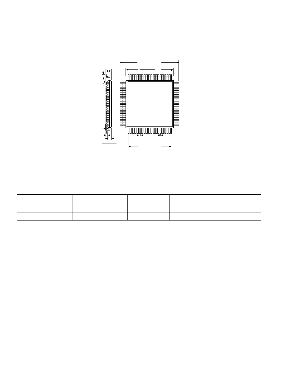
REV. 0
40
ADSP-21msp58/59
ORDERING GUIDE*
Ambient
Instruction
Temperate
Rate
Package
Package
Part Number
Range
(MIPS)
Description
Option
ADSP-21msp58BST-104
40
°
C to +85
°
C
26
100-Lead TQFP
ST-100
*Refer to the section titled "Ordering Procedure for ADSP-21msp59 ROM Processors" for information about ordering ROM coded parts.
PRINTED IN U.S.A.
C203044/95
OUTLINE DIMENSIONS
Dimensions shown in millimeters and (inches)
100-Lead Metric Thin Plastic Quad Flat Pack (TQFP)
SEATING
PLANE
0.75 (0.030)
0.50 (0.019)
1.60 (0.063)
MAX
0.15 (0.006)
0.05 (0.002)
0.057 (1.45)
0.053 (1.35)
0.1 (0.004)
TOP VIEW
(PINS DOWN)
1
25
26
51
50
75
100
76
0.27 (0.011)
0.17 (0.007)
16.25 (0.640)
15.75 (0.620)
SQ
14.05 (0.553)
13.95 (0.549)
SQ
0.56 (0.022)
0.44 (0.018)
12.06 (0.475) SQ