 | ÐлекÑÑоннÑй компоненÑ: DA4410-6 | СкаÑаÑÑ:  PDF PDF  ZIP ZIP |
ADA4410-6 Integrated Video Filter with Selectable Cutoff Frequencies for RGB, HD/SD Y, C, and CV Data Sheet (Rev. B)
Integrated Video Filter with Selectable Cutoff
Frequencies for RGB, HD/SD Y, C, and CV
ADA4410-6
Rev. B
Information furnished by Analog Devices is believed to be accurate and reliable. However, no
responsibility is assumed by Analog Devices for its use, nor for any infringements of patents or other
rights of third parties that may result from its use. Specifications subject to change without notice. No
license is granted by implication or otherwise under any patent or patent rights of Analog Devices.
Trademarks and registered trademarks are the property of their respective owners.
One Technology Way, P.O. Box 9106, Norwood, MA 02062-9106, U.S.A.
Tel: 781.329.4700
www.analog.com
Fax: 781.461.3113
© 2006 Analog Devices, Inc. All rights reserved.
FEATURES
Sixth-order filters with selectable cutoff frequencies
36 MHz, 18 MHz, 9 MHz
Many video standards supported
RGB/YPbPr/YUV/SD/YC/CV
Ideal for resolutions up to 1080i
-1 dB bandwidth of 30 MHz for HD
2:1 multiplexers on all inputs
Selectable gain: ×2 or ×4
DC output offset adjust: ±0.5 V, input referred
Excellent video specifications
NTSC differential gain: 0.11%
NTSC differential phase: 0.25°
Low input bias current: 6.6 A
Wide supply range: +4.5 V to ±5 V
Rail-to-rail output
Typical output swing of 4.5 V p-p on single 5 V supply
Disable feature
APPLICATIONS
Set-top boxes
DVD players and recorders
HDTVs
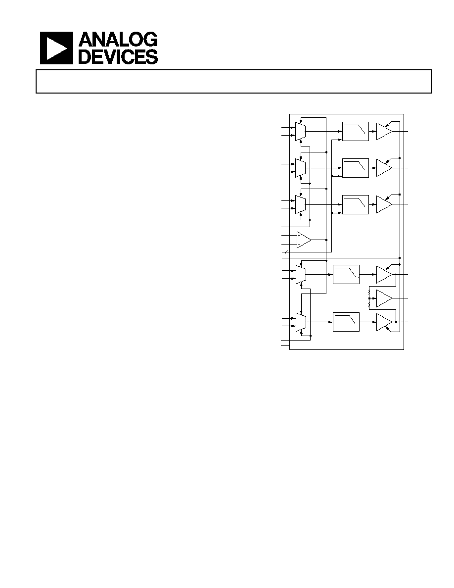
GENERAL DESCRIPTION
The ADA4410-6 is a comprehensive integrated filtering solution
that is carefully designed to give designers the flexibility to
easily filter and drive many types of video signals, including
high definition video. In the RGB/component channels, the
cutoff frequencies of the sixth-order filters can be selected by
two logic pins to obtain four filter combinations that are tuned
for RGB, high definition, and standard definition video. Cutoff
frequencies range from 9 MHz to 36 MHz.
The ADA4410-6 also provides filtering for the legacy standard
S-video and composite video signals. With a differential gain of
0.11% and a differential phase of 0.25°, the ADA4410-6 is an
excellent choice for any composite video (CV) application.
The ADA4410-6 offers gain and output offset voltage
adjustments. With a single logic pin, the gain of the part can be
selected to be ×2 or ×4. Output offset voltage is continuously
adjustable over an input-referred range of ±500 mV by applying
a differential voltage to an independent offset control input.
FUNCTIONAL BLOCK DIAGRAM
36MHz,
18MHz,
9MHz
36MHz,
18MHz,
9MHz
36MHz,
18MHz,
9MHz
9MHz
9MHz
Y1/G1 IN
Y2/G2 IN
×2
×4
Y/G OUT
Pb1/B1 IN
Pb2/B2 IN
×2
×4
Pb/B OUT
Pr1/R1 IN
Pr2/R2 IN
LEVEL1
DC
OFFSET
HD INPUT SELECT
LEVEL2
CUTOFF SELECT
GAIN SELECT
×2
×4
Pr/R OUT
Y1 IN
Y2 IN
×2
×4
Y OUT
C1 IN
C2 IN
SD INPUT SELECT
DISABLE
×2
×4
C OUT
×2
CV OUT
2
ADA4410-6
0
5265-
001
Figure 1.
The ADA4410-6 offers 2:1 multiplexers on its inputs that can be
used in applications where multiple sources of video exist.
The ADA4410-6 can operate on a single +5 V supply as well as
±5 V supplies. Single-supply operation is ideal for applications
where power consumption is critical. The disable feature allows
for further power conservation by reducing the supply current
to typically 15 A when a particular device is not in use.
Dual-supply operation is best for applications where the
negative-going excursions of the signal must swing at or below
ground while maintaining excellent video performance. The
output buffers have the ability to drive two 75 doubly
terminated cables that are either dc- or ac-coupled.
The ADA4410-6 is available in a 32-lead LFCSP and operates in
the extended industrial temperature range of -40°C to +85°C.

ADA4410-6
Rev. B | Page 2 of 16
TABLE OF CONTENTS
Features .............................................................................................. 1
Applications....................................................................................... 1
General Description ......................................................................... 1
Functional Block Diagram .............................................................. 1
Revision History ............................................................................... 2
Specifications..................................................................................... 3
Absolute Maximum Ratings............................................................ 7
Thermal Resistance ...................................................................... 7
ESD Caution.................................................................................. 7
Pin Configuration and Function Descriptions............................. 8
Typical Performance Characteristics ............................................. 9
Theory of Operation ...................................................................... 12
Applications..................................................................................... 13
Overview ..................................................................................... 13
Multiplexer Select Inputs........................................................... 13
Throughput Gain........................................................................ 13
Disable ......................................................................................... 13
Cutoff Frequency Selection....................................................... 13
Output DC Offset Control ........................................................ 13
Input and Output Coupling ...................................................... 14
Printed Circuit Board Layout ................................................... 15
Video Encoder Reconstruction Filter...................................... 15
Outline Dimensions ....................................................................... 16
Ordering Guide .......................................................................... 16
REVISION HISTORY
3/06--Rev. A to Rev. B
Changes to Table 1............................................................................ 3
Changes to Table 2............................................................................ 5
Changes to Figure 4 through Figure 9 ........................................... 9
Changes to Figure 10...................................................................... 10
Changes to Ordering Guide .......................................................... 16
Updated Outline Dimensions ....................................................... 16
8/05--Rev. 0 to Rev. A
Changes to Features, General Description, and Figure 1.............1
Changes to Table 1.............................................................................3
Changes to Table 2.............................................................................5
Changes to Figure 4...........................................................................9
Changes to Theory of Operation Section.................................... 12
Changes to Overview, Throughput Gain, and Output DC
Offset Control Sections.................................................................. 13
Renamed Gain Select Section Throughput Gain Section ........ 13
Added Composite Video Path Gain Section............................... 13
Changes to Table 6 and Table 7 .................................................... 13
Changes to Figure 24 Caption ...................................................... 14
Changes to Input and Output Coupling Section........................ 14
Added Figure 25 and Figure 26; Renumbered Sequentially ..... 14
Changes to Figure 27...................................................................... 15
1/05--Revision 0: Initial Version

ADA4410-6
Rev. B | Page 3 of 16
SPECIFICATIONS
V
S
= 5 V, @ T
A
= 25°C, V
O
= 1.4 V p-p, G = ×2, R
L
= 150 , unless otherwise noted.
Table 1.
Parameter Test
Conditions/Comments
Min
Typ
Max
Unit
OVERALL
PERFORMANCE
Offset Error
Input referred, all channels except CV
10
32
mV
Input referred, CV
12
40
mV
Max Voltage Across LEVEL1 and LEVEL2 Inputs
±500
mV
Input Voltage Range, All Inputs
V
S-
- 0.1
V
S+
- 2.0
V
Output Voltage Swing, All Outputs
Positive swing
V
S+
- 0.35
V
S+
- 0.25
V
Negative
swing
V
S-
+ 0.10
V
S-
+ 0.3
V
Linear Output Current per Channel
30
mA
Integrated Voltage Noise, Referred to Input
All channels except CV
500
V
rms
Filter Input Bias Current
All channels
6.6
15
A
Total Harmonic Distortion at 1 MHz
F
C
= 36 MHz, F
C
= 18 MHz/F
C
= 9 MHz
0.01/0.07
%
RGB/YPbPr CHANNEL DYNAMIC PERFORMANCE
-1 dB Bandwidth
Cutoff frequency select = 36 MHz
31
MHz
Cutoff frequency select = 18 MHz
15
MHz
Cutoff frequency select = 9 MHz
8
MHz
-3 dB Bandwidth
Cutoff frequency select = 36 MHz
34
36
MHz
Cutoff frequency select = 18 MHz
16
18
MHz
Cutoff frequency select = 9 MHz
8
9
MHz
Out-of-Band Rejection
f = 75 MHz
-33
-42
dB
Crosstalk
f = 5 MHz, F
C
= 36 MHz
-68
dB
Input Mux Isolation
f = 1 MHz, R
SOURCE
= 300
86
dB
Propagation Delay
f = 16 MHz, F
C
= 36 MHz
20.5
ns
Group Delay Variation
Cutoff frequency select = 36 MHz
9.5
ns
Cutoff frequency select = 18 MHz
16.5
ns
Cutoff frequency select = 9 MHz
29.5
ns
Y/C SD CHANNEL DYNAMIC PERFORMANCE
-1 dB Bandwidth
7.5
MHz
-3 dB Bandwidth
8
9
MHz
Out-of-Band Rejection
f = 27 MHz
-56
dB
Propagation Delay
f = 1 MHz
72
ns
Group Delay Variation
30
ns
Crosstalk
f = 1 MHz
-72
dB
Input Mux Isolation
f = 1 MHz, R
SOURCE
= 75
77
dB
Y/C, CV OUTPUT VIDEO PERFORMANCE
Differential Gain
NTSC
0.09
%
Differential Phase
NTSC
0.37
Degrees
CONTROL INPUT PERFORMANCE
Input Logic 0 Voltage
All inputs except DISABLE
0.8
V
Input Logic 1 Voltage
All inputs except DISABLE
2.0
V
Input Bias Current
All inputs except DISABLE
7
15
A
DISABLE
PERFORMANCE
DISABLE Assert Voltage
V
S+
- 0.5
V
DISABLE Assert Time
100
ns
DISABLE Deassert Time
130
ns
DISABLE Input Bias Current
12
20
A
Input-to-Output Isolation--Disabled
100
dB

ADA4410-6
Rev. B | Page 4 of 16
Parameter Test
Conditions/Comments
Min
Typ
Max
Unit
POWER
SUPPLY
Operating Range
4.5
12
V
Quiescent Current
82
88
mA
Quiescent Current--Disabled
15
150
A
PSRR, Positive Supply
All channels except CV
62
72
dB
CV
channel
59 66 dB
PSRR, Negative Supply
All channels except CV
55
62
dB
CV
channel
52 56 dB

ADA4410-6
Rev. B | Page 5 of 16
V
S
= ±5 V, @ T
A
= 25°C, V
O
= 1.4 V p-p, G = ×2, R
L
= 150 , unless otherwise noted.
Table 2.
Parameter Test
Conditions/Comments
Min
Typ
Max
Unit
OVERALL
PERFORMANCE
Offset Error
Input referred, all channels except CV
14
33.5
mV
Input referred, CV
15
42.5
mV
Max Voltage Across LEVEL1 and LEVEL2 Inputs
±500
mV
Input Voltage Range, All Inputs
V
S-
- 0.1
V
S+
- 2.0
V
Output Voltage Swing, All Outputs
Positive swing
V
S+
- 0.35
V
S+
- 0.25
V
Negative
swing
V
S-
+ 0.3
V
S-
+ 0.5
V
Linear Output Current per Channel
30
mA
Integrated Voltage Noise, Referred to Input
All channels except CV
500
V
rms
Filter Input Bias Current
All channels
6.3
15
A
Total Harmonic Distortion at 1 MHz
F
C
= 36 MHz, F
C
= 18 MHz/F
C
= 9 MHz
0.01/0.07
%
RGB/YPbPr CHANNEL DYNAMIC PERFORMANCE
-1 dB Bandwidth
Cutoff frequency select = 36 MHz
29
MHz
Cutoff frequency select = 18 MHz
15
MHz
Cutoff frequency select = 9 MHz
8
MHz
-3 dB Bandwidth
Cutoff frequency select = 36 MHz
33.0
35.5
MHz
Cutoff frequency select = 18 MHz
16.5
18
MHz
Cutoff frequency select = 9 MHz
8
9.5
MHz
Out-of-Band Rejection
f = 75 MHz
-33
-41.5
dB
Crosstalk
f = 5 MHz, F
C
= 36 MHz
-68
dB
Input Mux Isolation
f = 1 MHz, R
SOURCE
= 300
86
dB
Propagation Delay
f = 5 MHz, F
C
= 36 MHz
21
ns
Group Delay Variation
Cutoff frequency select = 36 MHz
7.5
ns
Cutoff frequency select = 18 MHz
14
ns
Cutoff frequency select = 9 MHz
26
ns
Y/C SD CHANNEL DYNAMIC PERFORMANCE
-1 dB Bandwidth
7.5
MHz
-3 dB Bandwidth
8
9
MHz
Out-of-Band Rejection
f = 27 MHz
-57
dB
Propagation Delay
f = 1 MHz
64
ns
Group Delay Variation
26
ns
Crosstalk
f = 1 MHz
-72
dB
Input Mux Isolation
f = 1 MHz, R
SOURCE
= 75
77
dB
Y/C, CV OUTPUT VIDEO PERFORMANCE
Differential Gain
NTSC
0.11
%
Differential Phase
NTSC
0.25
Degrees
CONTROL INPUT PERFORMANCE
Input Logic 0 Voltage
All inputs except DISABLE
0.8
V
Input Logic 1 Voltage
All inputs except DISABLE
2.0
V
Input Bias Current
All inputs except DISABLE
7
15
A
DISABLE
PERFORMANCE
DISABLE Assert Voltage
V
S+
- 0.5
V
DISABLE Assert Time
75
ns
DISABLE Deassert Time
125
ns
DISABLE Input Bias Current
35
45
A
Input-to-Output Isolation--Disabled
100
dB
Document Outline
- þÿ
- þÿ
- þÿ
- FUNCTIONAL BLOCK DIAGRAM
- þÿ
- þÿ
- þÿ
- þÿ
- þÿ
- þÿ
- þÿ
- þÿ
- þÿ
- þÿ
- þÿ
- þÿ
- þÿ
- þÿ
- þÿ
- PRINTED CIRCUIT BOARD LAYOUT
- þÿ
- þÿ