 | ÐлекÑÑоннÑй компоненÑ: DAC10F | СкаÑаÑÑ:  PDF PDF  ZIP ZIP |
DAC10 Data Sheet
REV. D
Information furnished by Analog Devices is believed to be accurate and
reliable. However, no responsibility is assumed by Analog Devices for its
use, nor for any infringements of patents or other rights of third parties
which may result from its use. No license is granted by implication or
otherwise under any patent or patent rights of Analog Devices.
a
DAC10*
One Technology Way, P.O. Box 9106, Norwood, MA 02062-9106, U.S.A.
Tel: 781/329-4700
World Wide Web Site: http://www.analog.com
Fax: 781/326-8703
© Analog Devices, Inc., 1998
10-Bit High Speed Multiplying D/A Converter
(Universal Digital Logic Interface)
FEATURES
Fast Settling: 85 ns
Low Full-Scale Drift: 10 ppm/ C
Nonlinearity to 0.05% Max Over Temperature Range
Complementary Current Outputs: 0 mA to 4 mA
Wide Range Multiplying Capability: 1 MHz Bandwidth
Wide Power Supply Range: +5, 7.5 Min to 18 V Max
Direct Interface to TTL, CMOS, ECL, PMOS, NMOS
Availability in Die Form
GENERAL DESCRIPTION
The DAC10 series of 10-bit monolithic multiplying digital-to-
analog converters provide high speed performance and full-scale
accuracy.
Advanced circuit design achieves 85 ns settling times with very
low "glitch" energy and low power consumption. Direct inter-
face to all popular logic families with full noise immunity is
provided by the high swing, adjustable threshold logic inputs.
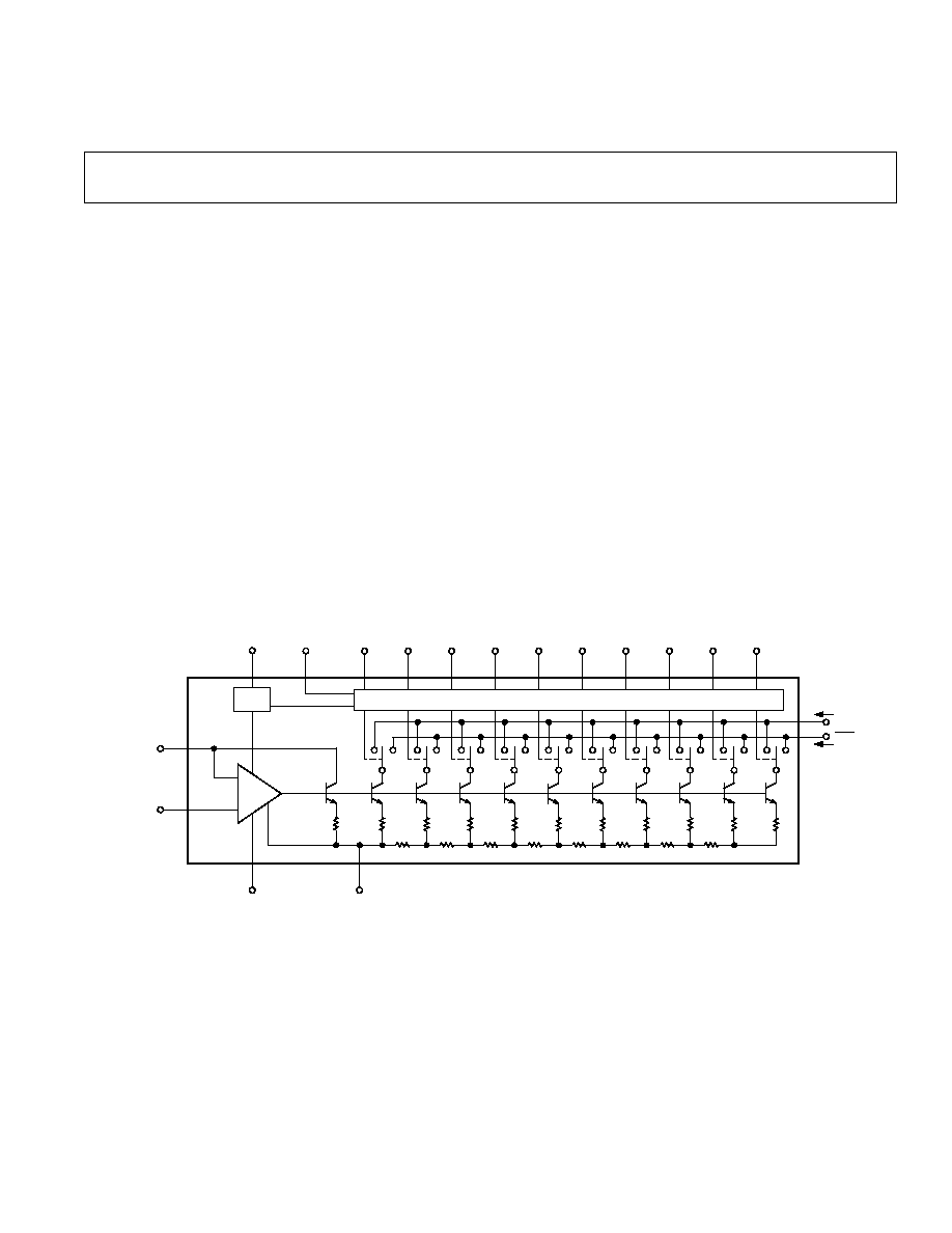
SIMPLIFIED SCHEMATIC
2
4
I
OUT
I
OUT
V+
V
LC
MSB
B
1
B
2
B
3
B
4
B
5
B
6
B
7
B
8
B
9
B
10
LSB
15
1
5
6
7
8
9
10
11
12
13
14
BIAS NETWORK
CURRENT SWITCHES
REFERENCE
AMPLIFIER
16
17
V
REF
(+)
V
REF
()
COMP
V
18
3
All DAC10 series models guarantee full 10-bit monotonicity,
and nonlinearities as tight as +0.05% over the entire operating
temperature range are available. Device performance is essen-
tially unchanged over the
±
18 V power supply range, with
85 mW power consumption attainable at lower supplies.
A highly stable, unique trim method is used, which selectively
shorts Zener diodes, to provide 1/2 LSB full-scale accuracy
without the need for laser trimming.
Single-chip reliability, coupled with low cost and outstanding
flexibility, make the DAC10 device an ideal building block for
A/D converters, Data Acquisition systems, CRT displays, pro-
grammable test equipment and other applications where low
power consumption, input/output versatility and long-term
stability are required.
*Protected by Patent Nos. 4,055,770, 4,056,740 and 4,092,639.
REV. D
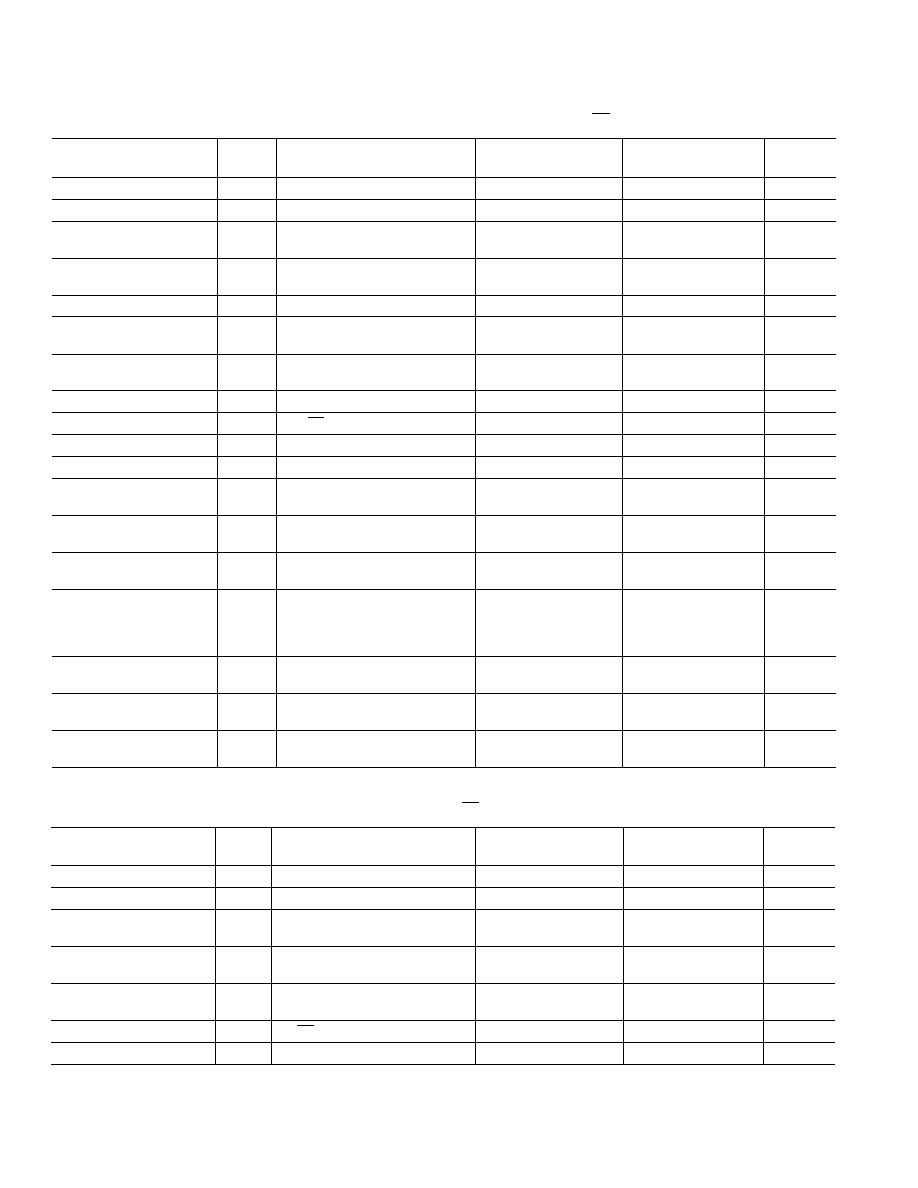
DAC10SPECIFICATIONS
2
ELECTRICAL CHARACTERISTICS
DAC10F
DAC10G
Parameter
Symbol
Conditions
Min
Typ
Max
Min
Typ
Max
Units
MONOTONICITY
10
10
Bits
NONLINEARITY
NL
0.3
0.5
0.6
1
LSB
DIFFERENTIAL
NONLINEARITY
DNL
0.3
1
0.7
LSB
SETTLING TIME
t
S
All Bits Switched ON or OFF
Settle to 0.05% of FS (See Note)
85
135
85
150
ns
OUTPUT CAPACITANCE
C
O
18
18
pF
PROPAGATION DELAY
t
PLH
All Bits Switched
R
L
= 5 k
50
50
ns
t
PHL
R
L
= 0 k
50
50
ns
OUTPUT VOLTAGE
Full-Scale Current Change
5.5
5.5
V
COMPLIANCE
V
OC
<1 LSB
+10
+10
V
GAIN TEMPCO
TCI
FS
(See Note)
±
10
±
25
±
10
±
50
ppm/
°
C
FULL-SCALE SYMMETRY
I
FSS
I
FR
I
FR
0.1
4
0.1
4
µ
A
ZERO-SCALE CURRENT
I
ZS
0.01
0.5
0.01
0.5
µ
A
FULL-SCALE CURRENT
I
FR
(See Note)
3.960
3.996
4.032
3.920
3.996
4.072
mA
REFERENCE INPUT
SLEW RATE
DI/dt
6
6
mA/
µ
s
REFERENCE BIAS
CURRENT
I
B
1
3
1
3
µ
A
POWER SUPPLY
PPS/
FS
+
4.5 V
V+
18 V
0.001
0.01
0.001
0.01
%
I
FS
/%
V
SENSITIVITY
PPS/
FS
18 V
V
10 V
0.0012 0.01
0.0012 0.01
%
I
FS
/%
V
POWER SUPPLY CURRENT I+
V
S
=
±
15 V; I
REF
= 2 mA
2.3
4
2.3
4
mA
I
9
15
9
15
mA
I+
V
S
= +5 V; 7.5 V; I
REF
= 1 mA
1.8
4
1.8
4
mA
I
5.9
9
5.9
9
mA
POWER DISSIPATION
P
D
V
S
=
±
15 V; I
REF
= 2 mA
231
285
231
285
mW
P
D
V
S
= +5 V; 7.5 V; I
REF
= 1 mA
85
88
85
88
mW
LOGIC INPUT LEVELS
V
IL
V
LC
= 0
0.8
0.8
V
V
IH
V
LC
= 0
2
2
V
LOGIC INPUT CURRENTS
I
IL
V
LC
= 0; V
IN
= 0.8 V
10
5
10
5
µ
A
I
IH
V
IN
= 2.0 V
0.001
10
0.001
10
µ
A
ELECTRICAL CHARACTERISTICS
DAC10F
DAC10G
Parameter
Symbol Conditions
Min
Typ
Max
Min
Typ
Max
Units
MONOTONICITY
10
10
Bits
NONLINEARITY
NL
0.3
0.5
0.6
1
LSB
DIFFERENTIAL
NONLINEARITY
DNL
0.3
1
0.7
LSB
OUTPUT VOLTAGE
COMPLIANCE
V
OC
Full-Scale Current Change, <1 LSB
5
6/+18 +10
5
6/+15 +10
V
FULL-SCALE CURRENT
I
FS
V
REF
= 10.000 V,
R14 = R15 = 5.000 k
3.978
3.996
4.014
3.956
3.996
4.036
mA
FULL-SCALE SYMMETRY
I
FSS
I
FR
I
FR
0.1
4
0.1
0.4
µ
A
ZERO-SCALE CURRENT
I
ZS
0.01
0.5
0.01
0.5
µ
A
NOTE: Guaranteed by design.
(@ V
S
= 15 V; I
REF
= 2 mA; 0 C
T
A
+70 C for DAC10F and G, unless otherwise noted.
Output characteristics apply to both I
OUT
and I
OUT
.)
(@ V
S
= 15 V; I
REF
= 2 mA; T
A
= +25 C, unless otherwise noted. Output characteristics
apply to both I
OUT
and I
OUT
.)
3
REV. D
DAC10
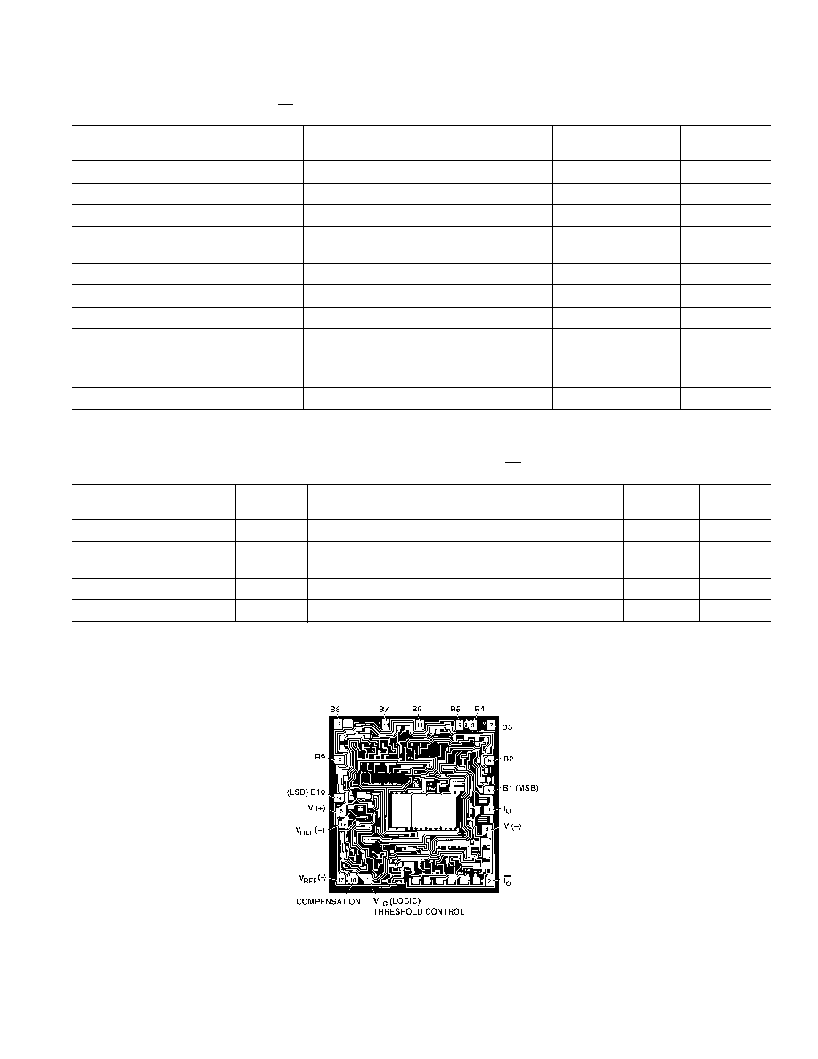
WAFER TEST LIMITS
DAC10N
Parameter
Symbol
Conditions
Limit
Units
RESOLUTION
10
Bits min
MONOTONICITY
10
Bits min
NONLINEARITY
NL
±
0.5
LSB max
OUTPUT VOLTAGE COMPLIANCE
V
OC
True 1 LSB
+10
V max
5
V min
OUTPUT CURRENT RANGE
I
FS
±
3.996 mA
±
18
µ
A max
ZERO-SCALE CURRENT
I
ZS
All Bits OFF
0.5
µ
A max
LOGIC INPUT "1"
V
IH
I
IN
= 100 nA
2
V min
LOGIC INPUT "0"
V
IL
V
LC
@ Ground
0.8
V max
I
IN
= 100
µ
A
POSITIVE SUPPLY CURRENT
I+
V+ = 15 V
4
mA max
NEGATIVE SUPPLY CURRENT
I
V+ = 15 V
15
mA max
NOTE: Electrical tests are performed at wafer probe to the limits shown. Due to variations in assembly methods and normal yield loss, yield after packaging is not
guaranteed for standard produce dice.
TYPICAL ELECTRICAL CHARACTERISTICS
DAC10F
Parameter
Symbol
Conditions
Typ
Units
SETTLING TIME
t
S
To
±
1/2 LSB When Output Is Switched from 0 to FS
85
ns
GAIN TEMPERATURE
COEFFICIENT (TC)
V
REF
Tempco Excluded
±
10
ppm FS/
°
C
OUTPUT CAPACITANCE
18
pF
OUTPUT RESISTANCE
10
M
(@ V
S
= 15 V, I
REF
= 2 mA, T
A
= +25 C, unless otherwise noted. Output characteristics refer to both
I
OUT
and I
OUT
).
(@ V
S
=
15 V, I
REF
= 2 mA, unless otherwise noted. Output characteristics
refer to both I
OUT
and I
OUT
).
DICE CHARACTERISTICS
DIE SIZE 0.091 0.087 inch, 7,917 sq. mils
(2.311 2.210 mm, 5.107 sq. mm)
DAC10
4
REV. D
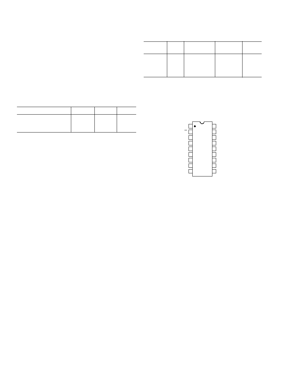
ABSOLUTE MAXIMUM RATINGS
1
Operating Temperature
DAC10FX, GX, GS, GP . . . . . . . . . . . . . . . . 0
°
C to +70
°
C
Junction Temperature (T
J
) . . . . . . . . . . . . . 65
°
C to +150
°
C
Storage Temperature . . . . . . . . . . . . . . . . . . 65
°
C to +150
°
C
Lead Temperature (Soldering, 60 sec) . . . . . . . . . . . +300
°
C
V+ Supply to V Supply . . . . . . . . . . . . . . . . . . . . . . . . . 36 V
Logic Inputs . . . . . . . . . . . . . . . . . . . . . . V to V plus 36 V
V
LC
. . . . . . . . . . . . . . . . . . . . . . . . . . . . . . . . . . . . . V to V+
Analog Current Outputs . . . . . . . . . . . . . . . . +18 V to 18 V
Reference Inputs (V
16
to V
17
) . . . . . . . . . . . . . . . . . V to V+
Reference Input Differential Voltage (V
16
to V
17
) . . . .
±
18 V
Reference Input Current (I
16
) . . . . . . . . . . . . . . . . . . 2.5 mA
Package Type
JA
2
JC
Units
18-Lead Hermetic DIP (X)
48
15
°
C/W
18-Lead SOIC (S)
89
28
°
C/W
18-Lead Plastic DIP (P)
74
33
°
C/W
NOTES
1
Absolute maximum ratings apply to both DICE and packaged parts, unless
otherwise noted.
2
JA
is specified for worst case mounting conditions, i.e.,
JA
is specified for device
in socket for Cerdip packages.
ORDERING GUIDE
INL
Temperature
Package
Package
Model
(LSB)
Range
Description Options
DAC10FX
0.5
0
°
C to +70
°
C
Cerdip
Q-18
DAC10GX
1
0
°
C to +70
°
C
Cerdip
Q-18
DAC10GS
1
0
°
C to +70
°
C
SOIC
R-18
DAC10GP
1
0
°
C to +70
°
C
Plastic DIP
N-18
PIN CONNECTIONS
18-Lead Hermetic DIP
18-Lead Plastic DIP
18-Lead SOIC
TOP VIEW
(Not to Scale)
18
17
16
15
14
13
12
11
10
1
2
3
4
5
6
7
8
9
DAC10
B5
B4
V
LC
I
O
V
I
O
B3
B2
(MSB) B1
B6
B7
COMP
V
REF
()
V
REF
(+)
V+
B8
B9
B10 (LSB)
CAUTION
ESD (electrostatic discharge) sensitive device. Electrostatic charges as high as 4000 V readily
accumulate on the human body and test equipment and can discharge without detection.
BASIC CONNECTIONS
0mA
1.0mA
2.0mA
I
OUT
I
OUT
(0000000000)
(11111111111)
I
REF
= 2mA
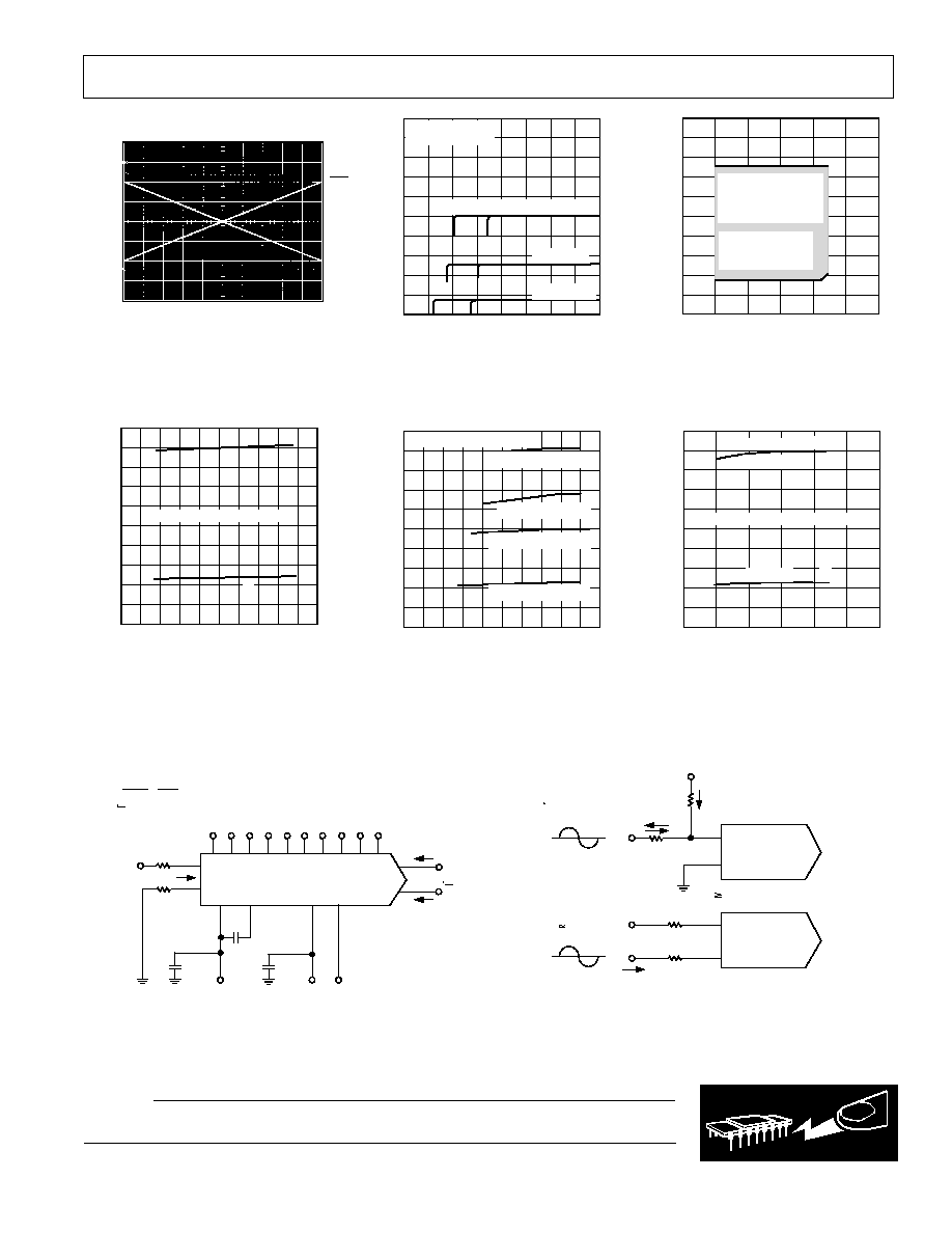
Figure 1. True and Complementary
Output Operations
V+, POSITIVE POWER SUPPLY V
DC
POWER SUPPLY CURRENT mA
10
3
0
0
2
20
4
6
8
10
12
14
16 18
9
4
2
1
6
5
8
7
ALL BITS "HIGH" OR "LOW"
I
I+
Figure 4. Power Supply Current
vs. V+
0.1 F
C
C
3
18
V+
0.01 F
15
COMP
B
1
5
6
B
2
B
3
7
8
B
4
9
B
5
10
B
6
11
B
7
12
B
8
13
B
9
14
B
10
V
LC
1
I
FR
=
+V
REF
R
REF
1023
1024
2
I
O
+ I
O
= I
FR
FOR ALL
LOGIC STATES
+V
REF
R
REF
(R16)
I
REF
R17
16
MSB
LSB
FOR FIXED REFERENCE,
TTL OPERATION,
TYPICAL VALUES ARE:
V
REF
= +10.000V
R
REF
= 5.000k
R15 = R
REF
C
C
= 0.01 F
V
LC
= 0V (GROUND)
I
O
I
O
4
2
17
DAC10
V
Figure 7. Basic Positive Reference Operation
Typical Performance CharacteristicsDAC10
5
REV. D
WARNING!
ESD SENSITIVE DEVICE
V = 15V, V = 10V
T
A
= T
MIN
TO T
MAX
ALL BITS ON
OUTPUT VOLTAGE Volts
OUTPUT CURRENT mA
8.0
0
14 10
18
6
2
2
6
10
14
7.2
4.8
4.0
2.4
0.8
6.4
5.6
3.2
1.6
I
REF
= 1mA
I
REF
= 2mA
I
REF
= 0.2mA
Figure 2. Output Current vs. Output
Voltage (Output Voltage Compliance)
POWER SUPPLY CURRENT mA
10
3
0
0
20
4
8
12
16
9
4
2
1
6
5
8
7
V, NEGATIVE POWER SUPPLY V
DC
BITS MAY BE HIGH OR LOW
I WITH I
REF
= 2mA
I WITH I
REF
= 1mA
I WITH I
REF
= 0.2mA
I WITH I
REF
= 0.2mA
Figure 5. Power Supply Current
vs. V
TEMPERATURE C
OUTPUT VOLTAGE Volts
+28
12
50
FOR OTHER V OR I
REF
SEE OUTPUT CURRENT
vs. OUTPUT VOLTAGE
CURVE
SHADED AREA INDICATES
PERMISSABLE OUTPUT
VOLTAGE RANGE
FOR V = 15V
I
REF
2.0mA
0
+50
+100
+150
+24
+4
0
4
8
+20
+16
+8
+12
Figure 3. Output Voltage Compliance
vs. Temperature
TEMPERATURE C
POWER SUPPLY CURRENT mA
10
0
50
0
+50
+100
+150
9
4
3
2
1
8
7
5
6
ALL BITS MAY BE "HIGH" OR "LOW"
V+ = +15V
I+
I
I
REF
= 2.0mA
V = 15V
Figure 6. Power Supply Current vs.
Temperature
DAC10
DAC10
16
17
16
17
V
IN
V
IN
I
IN
R
REF
R17
(OPTIONAL)
R
IN
I
REF
+V
REF
R
REF
R
REF
R17
+V
REF
I
REF
PEAK NEGATIVE SWING OF I
IN
+V
REF
MUST BE ABOVE PEAK POSITIVE SWING OF V
IN
HIGH INPUT
IMPEDANCE
Figure 8. Accommodating Bipolar References