REV. B
Information furnished by Analog Devices is believed to be accurate and
reliable. However, no responsibility is assumed by Analog Devices for its
use, nor for any infringements of patents or other rights of third parties
which may result from its use. No license is granted by implication or
otherwise under any patent or patent rights of Analog Devices.
a
16-Bit High Speed
Current-Output DAC
DAC16
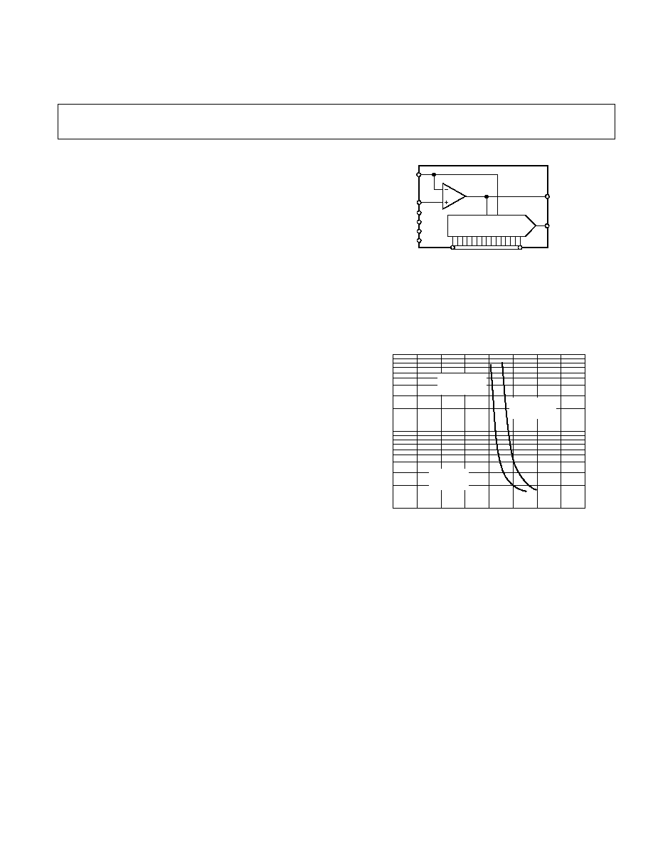
FUNCTIONAL BLOCK DIAGRAM
BUFFER
DAC
C
COMP
I
OUT
DB0 (LSB)
DB15 (MSB)
DAC16
I
REF
REF GND
V
CC
AGND
V
EE
DGND
GENERAL DESCRIPTION
The DAC16 is a 16-bit high speed current-output digital-to-
analog converter with a settling time of 500 ns. A unique com-
bination of low distortion, high signal-to-noise ratio, and high
speed make the DAC16 ideally suited to performing waveform
synthesis and modulation in communications, instrumentation,
and ATE systems. Input reference current is buffered, with full-
scale output current of 5 mA. The 16-bit parallel digital input
bus is TTL/CMOS compatible. Operating from +5 V and
�15 V supplies, the DAC16 consumes 190 mW (typ) and is
available in a 24-lead epoxy DIP, epoxy surface-mount small
outline (SOL), and in die form.
FEATURES
1 LSB Differential Linearity (max)
Guaranteed Monotonic Over Temperature Range
2 LSB Integral Linearity (max)
500 ns Settling Time
5 mA Full-Scale Output
TTL/CMOS Compatible
Low Power: 190 mW (typ)
Available in Die Form
APPLICATIONS
Communications
ATE
Data Acquisition Systems
High Resolution Displays
One Technology Way, P.O. Box 9106, Norwood, MA 02062-9106, U.S.A.
Tel: 781/329-4700
World Wide Web Site: http://www.analog.com
Fax: 781/326-8703
� Analog Devices, Inc., 1999
SETTLING TIME � ns
0.1
0.01
0.001
0
100
PERCENT OF FULL-SCALE � %
200
300
400
500
600
700
800
V
LOGIC
= 0V
TURNING ON
V
LOGIC
= +5V
TURNING OFF
I
FS
= 4mA
T
A
= 25 C
Figure 1. DAC16 Settling Time Accuracy vs. Percent of
Full Scale

DAC16�SPECIFICATIONS
ELECTRICAL CHARACTERISTICS
Parameter
Conditions
Min
Typ
Max
Units
Integral Linearity "G"
INL
T
A
= +25
�
C
�2
�
1.2
+2
LSB
Integral Linearity "G"
INL
�4
�
1.6
+4
LSB
Differential Linearity "G"
DNL
T
A
= +25
�
C
�1
�
0.5
+1
LSB
Differential Linearity "G"
DNL
�1
�
0.7
+1.5
LSB
Integral Linearity "F"
INL
T
A
= +25
�
C
�4
�
1.4
+4
LSB
Integral Linearity "F"
INL
�6
�
2
+6
LSB
Differential Linearity "F"
DNL
T
A
= +25
�
C
�1
�
0.5
+1.5
LSB
Differential Linearity "F"
DNL
�1.5
�
0.6
+2
LSB
Zero Scale Error
ZSE
1
LSB
Zero Scale Drift
TC
ZSE
0.025
ppm/
�
C
Gain Error
GE
�
0.225
% FS
Gain Drift
TC
GE
5
ppm/
�
C
REFERENCE
2
Reference Input Current
I
REF
Note 2
350
625
�
A
OUTPUT CHARACTERISTICS
Output Current
I
OUT
Note 2
2.8
5.0
mA
Output Capacitance
C
OUT
10
pF
Settling Time
t
S
0.003% of Full Scale
500
ns
LOGIC CHARACTERISTICS
Logic Input High Voltage
V
INH
T
A
= +25
�
C
2.4
V
Logic Input Low Voltage
V
INL
T
A
= +25
�
C
0.8
V
Logic Input Current
I
INH
V
IN
= 5.0 V, DB0�DB10
7.5
�
A
Logic Input Current
I
INH
V
IN
= 5.0 V, DB11�DB15
100
�
A
Logic Input Current
I
INL
V
IN
= 0 V, DB0�DB15
1
�
A
Input Capacitance
C
IN
8
pF
SUPPLY CHARACTERISTICS
Power Supply Sensitivity
PSS
V
CC
= 4.5 V to 5.5 V, V
EE
= �13 V to �17 V
20
ppm/V
Positive Supply Current
I
CC
All Bits HIGH
15
22
mA
Positive Supply Current
I
CC
All Bits LOW
6
7.5
mA
Negative Supply Current
I
EE
7.5
10
mA
Power Dissipation
P
DISS
188
260
mW
NOTES
1
All supplies can be varied
�
5% and operation is guaranteed. Device is tested with nominal supplies.
2
Operation is guaranteed over this reference range, but linearity is neither tested not guaranteed (see Figures 7 and 8).
Specifications subject to change without notice.
WAFER TEST LIMITS
DAC16G
Parameter
Symbol
Conditions
Limit
Units
Integral Nonlinearity
INL
�
3
LSB max
Differential Nonlinearity
DNL
�
1
LSB max
Zero Scale Error
ZSE
�
1
LSB max
Gain Error
GE
�
12
% FS max
Logic Input High Voltage
V
INH
2.4
V min
Logic Input Low Voltage
V
INL
0.8
V max
Logic Input Current
I
IN
75
�
A max
Positive Supply Current
I
CC
20
mA max
Negative Supply Current
I
EE
10
mA max
Power Dissipation
P
DISS
250
mW max
NOTE
Electrical tests are performed at wafer probe to the limits shown. Due to variations in assembly methods and normal yield loss, yield after packaging is not guaranteed
for standard product dice. Consult factory to negotiate specifications based on dice lot qualification through sample lot assembly and testing.
REV. B
�2�
(@ V
CC
= +5.0 V, V
EE
= �15.0 V, I
REF
= 0.5 mA, C
COMP
= 47 F, T
A
= Full Operating Tem-
perature Range unless otherwise noted. See Note 1 for supply variations.)
(@ V
CC
= +5.0 V, V
EE
= �15.0 V, I
REF
= 0.5 mA, C
COMP
= 47 F, T
A
= +25 C unless otherwise noted.)
DAC16
REV. B
�3�
CAUTION
1. Stresses above those listed under "Absolute Maximum Rat-
ings" may cause permanent damage to the device. This is a
stress rating only and functional operation at or above this
specification is not implied. Exposure to the above maximum
rating conditions for extended periods may affect device
reliability.
2. Digital inputs and outputs are protected; however, perma-
nent damage may occur on unprotected units from high en-
ergy electrostatic fields. Keep units in conductive foam or
packaging at all times until ready to use. Use proper anti-
static handling procedures.
3. Remove power before inserting or removing units from their
sockets.
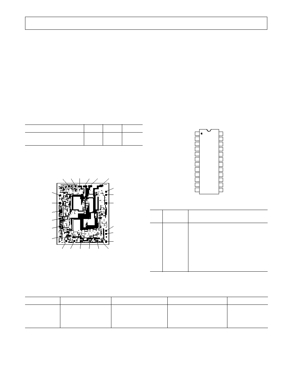
PIN CONFIGURATION
24-Lead DIP (P, S)
TOP VIEW
(Not to Scale)
24
23
22
21
20
19
18
17
16
15
14
13
1
2
3
4
5
6
7
8
9
10
11
12
DAC16
I
REF
C
COMP
DGND
V
CC
DB15 (MSB)
DB14
DB13
DB12
DB11
DB10
DB9
DB8
DB7
I
OUT
AGND
REF GND
V
EE
DB0 (LSB)
DB1
DB2
DB3
DB4
DB5
DB6
PIN DESCRIPTION
Pin
(P, S) Name
Description
1
I
REF
Reference Current Input
2
DGND
Digital Ground
3
V
CC
+5 V Digital Supply
4�19
DB15�DB0 16-Bit Digital Input Bus. DB15 is the MSB.
20
V
EE
�15 V Analog Supply
21
REF GND
Reference Current Return
22
AGND
Analog Ground/Output Reference
23
I
OUT
Current Output
24
C
COMP
Current Ladder Compensation
ORDERING GUIDE
Model
Grade DNL (max)
Temperature Ranges
Package Descriptions
Package Options
DAC16GS
�
1
0
�
C to +70
�
C
24-Lead SOL
R-24
DAC16FP
�
2
�40
�
C to +85
�
C
24-Lead PDIP
N-24
DAC16FS
�
2
�40
�
C to +85
�
C
24-Lead SOL
R-24
DAC16GBC
�
1
+25
�
C
Die
ABSOLUTE MAXIMUM RATINGS
(T
A
= +25
�
C unless otherwise noted)
V
CC
to V
EE
. . . . . . . . . . . . . . . . . . . . . . . . . . . �0.3 V, +25.0 V
V
CC
to DGND . . . . . . . . . . . . . . . . . . . . . . . . . �0.3 V, +7.0 V
V
EE
to AGND . . . . . . . . . . . . . . . . . . . . . . . . +0.3 V, �18.0 V
DGND to AGND . . . . . . . . . . . . . . . . . . . . . . �0.3 V, +0.3 V
REF GND to AGND . . . . . . . . . . . . . . . . . . . �0.3 V, +1.0 V
I
REF
. . . . . . . . . . . . . . . . . . . . . . . . . . . . . . . . . . . . . . . . . 1 mA
Analog Output Current . . . . . . . . . . . . . . . . . . . . . . . . . . 8 mA
Digital Input Voltage to DGND . . . . . . . . . . . . . . . . . . .
V
CC
Operating Temperature Range
FP, FS . . . . . . . . . . . . . . . . . . . . . . . . . . . . �40
�
C to +85
�
C
GS . . . . . . . . . . . . . . . . . . . . . . . . . . . . . . . . . 0
�
C to +70
�
C
Dice Junction Temperature . . . . . . . . . . . . . . . . . . . . . +150
�
C
Storage Temperature . . . . . . . . . . . . . . . . . . �65
�
C to +150
�
C
Power Dissipation . . . . . . . . . . . . . . . . . . . . . . . . . . 1000 mW
Lead Temperature (Soldering, 60 sec) . . . . . . . . . . . . +300
�
C
Package Type
JA
1
JC
Units
24-Lead Plastic DIP (P)
62
32
�
C/W
24-Lead Plastic SOL (S)
70
22
�
C/W
NOTE
1
JA
is specified for worst case mounting conditions, i.e.,
JA
is specified for
device in socket.
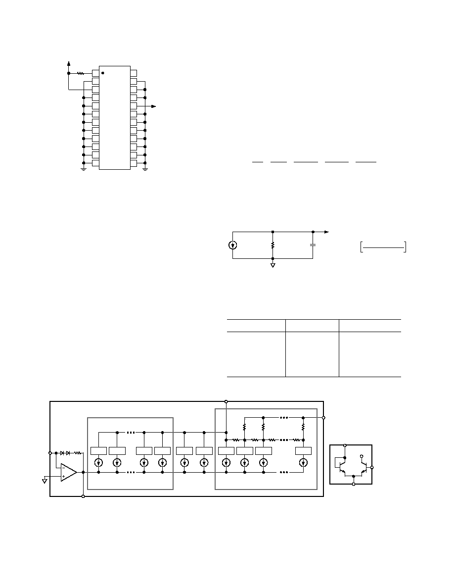
DICE CHARACTERISTICS
V
CC
DGND
I
REF
C
COMP
I
OUT
AGND
REF GND
V
EE
DB0 (LSB)
DB1
DB2
DB3
DB4
DB5
DB6
DB7
DB8
DB9
DB10
DB11
DB12
DB13
DB14
DB15 (MSB)
Die Size 0.129 x 0.153 inch, 19,737 sq. mils
(3.277 x 3.886 mm, 12.73 sq. mm)
The DAC16 Contains 330 Transistors.
Substrate is V
EE
Polarity.
DAC16
REV. B
�4�
1
2
3
4
5
6
7
8
9
10
11
12
24
23
22
21
20
19
18
17
16
15
14
13
NC
10k
+5V
�15V
Figure 2. Burn-In Diagram
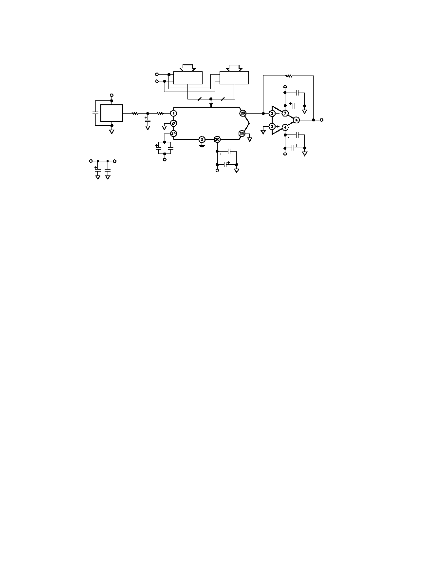
OPERATION
Novel DAC Architecture
The DAC16 was designed with a compound DAC architecture
to achieve high accuracy, excellent linearity, and low transition
errors. As shown in Figure 3, the DAC's five most-significant
bits utilize 31 identical segmented current sources to obtain
optimal high speed settling at major code transitions. The lower
nine bits utilize an inverted R-2R ladder network which is laser-
trimmed to ensure excellent differential nonlinearity. The middle
two bits (DB9 and DB10) arc binary-weighted and scaled from
the MSB segments. Note that the flow of output current is into
the DAC16--there is no signal inversion. As shown, the switches
for each current source are essentially diodes. It is for this rea-
son that the output voltage compliance of the DAC16 is limited
to a few millivolts. The DAC16 was designed to operate with an
operational amplifier configured as an I�V converter; therefore,
the DAC16's output must be connected to the sum node of an
operational amplifier for proper operation. Exceeding the output
voltage compliance of the DAC16 will introduce linearity errors.
The reference current buffer assures full accuracy and fast set-
tling by controlling the MSB reference node. The 16-bit paral-
lel digital input is TTL/CMOS compatible and unbuffered,
minimizing the deleterious effects of digital feedthrough
while allowing the user to tailor the digital interface to
the speed requirements and bus configuration of the
application.
Equivalent Circuit Analysis
An equivalent circuit for static operation of the DAC16 is
illustrated in Figure 4. I
REF
is the current applied to the
DAC16 and is set externally to the device by V
REF
and
R
REF
.
The output capacitance of the DAC16 is approxi-
mately 10 pF and is code independent. Its output resis-
tance R
O
is code dependent and is given by:
1
R
O
=
1
8
k
+
DB9
288
k
+
DB10
144
k
+
X
72
k
where
DB9 = State of Data Bit 9 = 0 or 1;
DB10 = State of Data Bit 10 = 0 or 1; and
X = Decimal representation of the 5 MSBs (DB11�DB15)
= 0 to 31.
I
DAC
R
O
C
O
I
OUT
I
OUT
= 8 � I
REF
R
O
= SEE TEXT
C
O
= 10pF
65,535 Digital Code
65,536
Figure 4. Equivalent Circuit for the DAC16
Table I provides the relationship between the input digital
code and the output resistance of the DAC16.
Table I. DAC16 Output Resistance vs. Digital Code
Hex Digital Code
Scale
Output Resistance
FFFF
Zero
8 k
BFFF
1/4
4.2 k
7FFF
1/2
2.9 k
3FFF
3/4
2.2 k
0
Full � 1 LSB
1.8 k
+5V
DB0 � DB15
SWITCH DETAIL
FROM
SWITCH
DECODER
4k
4k
8k
8k
DB0 � DB8
4k
4k
4k
SW10
SW9
SW8
SW7
SW6
SW0
SW
SW
SW
SW
18k
31 CURRENT SOURCES
125 A EACH
DB11 � DB15
DB10
DB9
9 CURRENT SOURCES
15.63 A EACH
I
REF
I
OUT
AGND
C
COMP
62.5 A 31.25 A
Figure 3. DAC16 Architecture
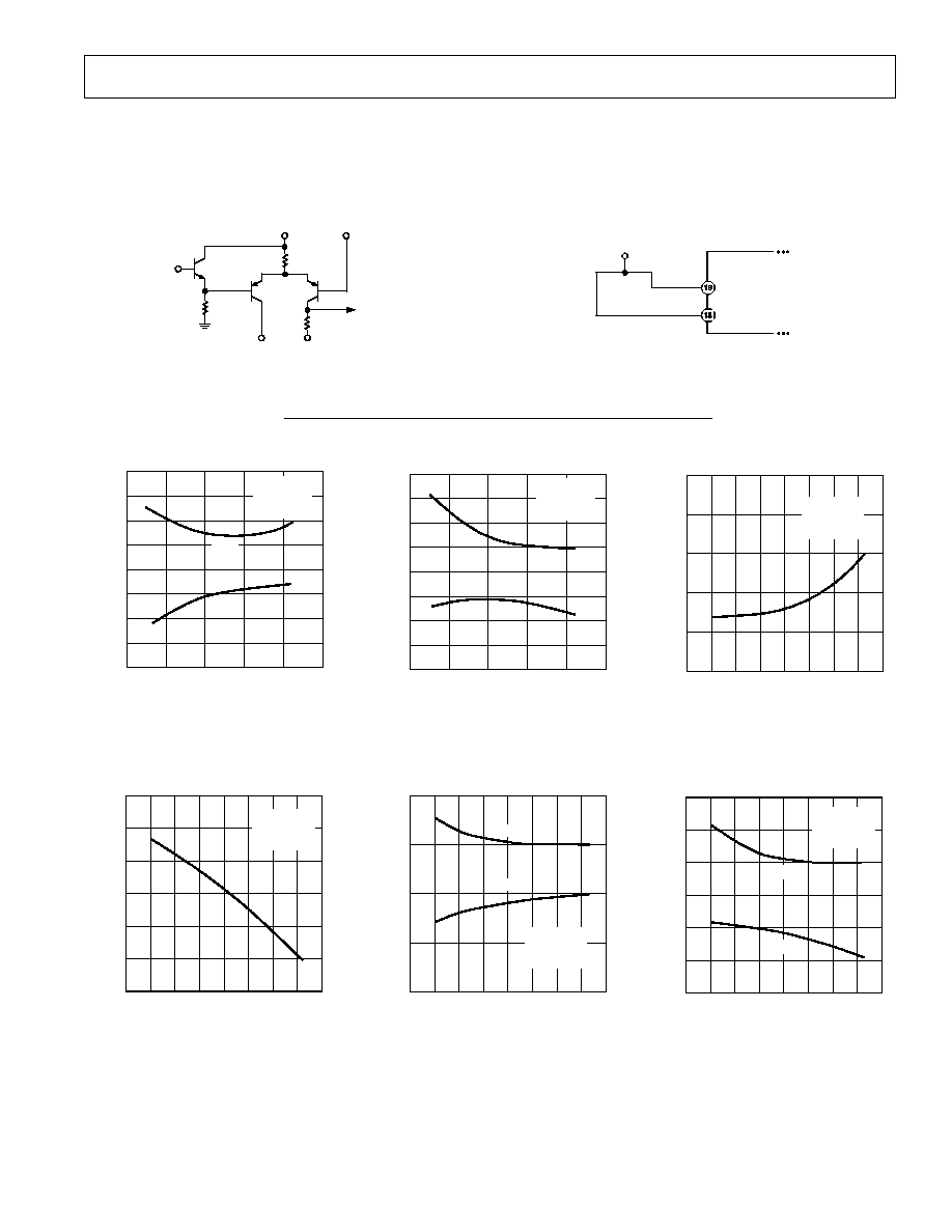
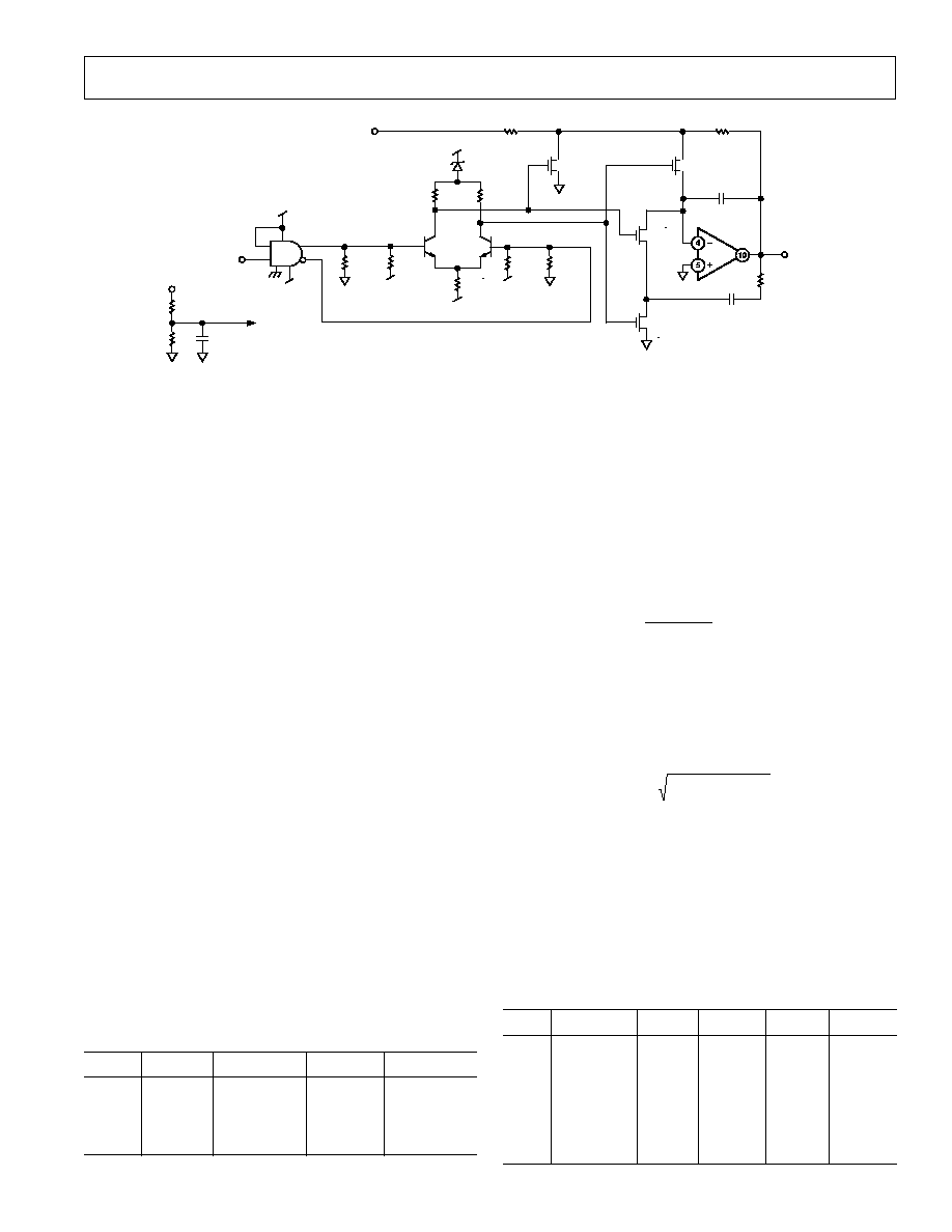
Digital Input Considerations
The threshold of the DAC16's digital input circuitry is set at
1.4 V, independent of supply voltage. Hence, the digital inputs
can interface with any type of 5 V logic. Illustrated in Figure 5 is
the equivalent circuit of the digital inputs. Note that the indi-
vidual input capacitance is approximately 7 pF.
Q3
Q2
Q1
R2
75k
R1
20k
R3
28k
TO DAC
SWITCH
+5V
+0.7V
�15V
�0.7V
DBX
Figure 5. Equivalent Circuit of a DAC16 Digital Input
This input capacitance can be used in conjunction with an ex-
ternal R-C circuit for digital signal deskewing, if required. In
applications where some of the DAC16's digital inputs are
not used, the recommended procedure to turn off one or more
inputs is to connect each input line to +5 V as shown in
Figure 6.
DB0
DB1
+5V
DAC16
Figure 6. Handling Unused DAC16 Digital Inputs
Typical Performance Characteristics�DAC16
REV. B
�5�
REFERENCE CURRENT � mA
DIFFERENTIAL NONLINEARITY � LSB
�2.0
0.2
0.3
0.4
0.5
0.6
0.7
V
CC
= +5V
V
EE
= �15V
T
A
= +25 C
�DNL
+DNL
�1.5
�1.0
�0.5
0
0.5
1.0
1.5
2.0
Figure 8. Differential Nonlinearity
vs. I
REF
TEMPERATURE � C
INTEGRAL NONLINEARITY � LSB
�40
�4
�20
0
20
40
60
80
�2
0
2
4
V
CC
= +5V
V
EE
= �15V
I
REF
= 0.5mA
+INL
�INL
Figure 11. Integral Nonlinearity
vs. Temperature
TEMPERATURE � C
ZERO SCALE � LSB
1.0
�40
0.8
0.6
0.4
0.2
0
�20
0
20
40
60
80
V
CC
= +5V
V
EE
= �15V
I
REF
= 0.5mA
Figure 9. Zero Scale Output vs.
Temperature
TEMPERATURE � C
DIFFERENTIAL NONLINEARITY � LSB
�40
�1.5
�20
0
20
40
60
80
V
CC
= +5V
V
EE
= �15V
I
REF
= 0.5mA
�1.0
�0.5
0
0.5
1.5
1.0
+DNL
�DNL
Figure 12. Differential Nonlinearity
vs. Temperature
REFERENCE CURRENT � mA
INTEGRAL NONLINEARITY � LSB
�4
0.2
�3
�2
�1
0
1
2
3
4
0.3
0.4
0.5
0.6
0.7
V
CC
= +5V
V
EE
= �15V
T
A
= +25 C
�INL
+INL
Figure 7. Integral Nonlinearity vs. I
REF
TEMPERATURE � C
GAIN ERROR � LSB
�40
�15
�20
0
20
40
60
80
V
CC
= +5V
V
EE
= �15V
I
REF
= 0.5mA
�10
�5
0
5
15
10
Figure 10. Gain Error vs.
Temperature
DAC16�Typical Performance Characteristics
REV. B
�6�
APPLICATIONS
Power Supplies, Bypassing, and Grounding
All precision converter products require careful application of
good grounding practices to maintain full-rated performance. As
is always the case with analog circuits operating in digital envi-
ronments, digital noise is prevalent; therefore, special care must
be taken to ensure that the DAC16's inherent precision is main-
tained. This means that particularly good engineering judgment
should be exercised when addressing the power supply, ground-
ing, and bypassing issues using the DAC16.
The DAC16 was designed to operate from +5 V and �15 V
supplies. The +5 V supply primarily powers the digital portion
of the DAC16 and can consume 20 mA, maximum. Although
very little +5 V supply current is used by the reference amplifier,
large amounts of digital noise present on the +5 V supply can
introduce analog errors. It is, therefore, very important that the
+5 V supply be well filtered and regulated. The �15 V supply
provides most of the current for the reference amplifier and all
of the current for the internal DAC. Although the maximum
current in this supply is 10 mA, it must provide a low imped-
ance path for the DAC switch currents. Therefore, it too must
be well filtered and regulated.
The DAC16 includes two ground connections in order to mini-
mize system accuracy degradation arising from grounding er-
rors. The two ground pins are designated DGND (Pin 2) and
AGND (Pin 22). The DGND pin is the return for the digital
circuit sections of the DAC and serves as their input threshold
reference point. Thus, DGND should be connected to the same
ground as the circuitry that drives the digital inputs.
Pin 22, AGND, serves as the reference point for the 9-bit
lower-order DAC as well as the common for the reference am-
plifier, REFGND (Pin 21). This pin should also serve as the
reference point for all analog circuitry associated with the
DAC16. Therefore, to minimize any errors, it is recommended
that AGND connection on the DAC16 be connected to a high
quality analog ground. If the system contains any analog signal
path carrying a significant amount of current, then that path
should have its own return connection to Pin 22.
It is often advisable to maintain separate analog and digital
grounds throughout a complete system, tying them common to
one place only. If the common tie point is remote and an acci-
dental disconnection of that one common tie point were to oc-
cur due to card removal with power on, a large differential
voltage between the two commons could develop. To protect
devices that interface to both digital and analog parts of the
TEMPERATURE � C
SUPPLY CURRENT � mA
�40
0
�20
0
20
40
60
80
5
10
15
20
I
CC
, LOGIC BITS = HIGH
I
EE
, LOGIC BITS = LOW
I
EE
, LOGIC BITS = HIGH
I
CC
, LOGIC BITS = LOW
Figure 13. Supply Current vs.
Temperature
BURN-IN TIME � Hours
DIFFERENTIAL NONLINEARITY � LSB
�1.5
0
�1.0
�0.5
0
0.5
1.0
1.5
200
400
600
800
1000
1200
V
CC
= +5V, V
EE
= �15V
T
A
= +25 C, I
REF
= 0.5mA
WORST CASE + DNL
TYPICAL + DNL
TYPICAL � DNL
WORST CASE � DNL
Figure 16. Differential Nonlinearity
vs. Time Accelerated by Burn-In
LOGIC INPUT VOLTAGE � V
ALL DATA BITS
I
CC
� mA
20
0
0
1
5
2
3
4
15
10
5
V
EE
= �15V
V
CC
= +5V
T
A
= +25 C
Figure 14. V
CC
Supply Current vs.
Logic Input Voltage, All Data Bits
BURN-IN TIME � Hours
INTEGRAL NONLINEARITY � LSB
�4
0
�3
�2
0
5
4
6
200
400
600
800
1000
1200
V
CC
= +5V, V
EE
= �15V
T
A
= +25 C, I
REF
= 0.5mA
WORST CASE + INL
TYPICAL + INL
TYPICAL � INL
WORST CASE � INL
�1
3
2
1
Figure 17. Integral Nonlinearity vs
Time Accelerated by Burn-In
TEMPERATURE � C
LOGIC BIT CURRENT �
A
50
�40
40
30
20
10
0
�20
0
20
40
60
80
V
CC
= +5V
V
EE
= �15V
V
IN
= +5V
DB0 � DB4
DB5 � DB15
Figure 15. Digital Input Current vs.
Temperature
BURN-IN TIME � Hours
GAIN ERROR � LSB
�30
0
�20
�10
0
110
120
130
200
400
600
800
1000
1200
V
CC
= +5V, V
EE
= �15V
T
A
= +25 C, I
REF
= 0.5mA
WORST CASE
+ GAIN ERROR
TYPICAL
GAIN ERROR
WORST CASE
� GAIN ERROR
Figure 18. Gain Error vs. Time
Accelerated by Burn-In
DAC16
REV. B
�7�
system, such as the DAC16, it is recommended that common
ground tie points be provided at each such device. If only one
system ground can be connected directly to the DAC16, it is
recommended that the analog common be used. If the system's
AGND has suitable low impedance, then the digital signal cur-
rents flowing in it should not seriously affect the ground noise.
The amount of digital noise introduced by connecting the two
grounds together at the device will not adversely affect system
performance due to loss of digital noise immunity.
Generous bypassing of the DAC's supplies goes a long way in
reducing supply-line induced errors. Even with well-filtered,
well-regulated supplies, local bypassing consisting of 10
�
F tan-
talum electrolytic shunted by a 0.1
�
F ceramic is recommended.
The decoupling capacitors should be connected between the
DAC's supply pins (Pin 3 for +5 V, Pin 20 for �15 V) and
the analog ground (Pin 22). Figure 19 shows how the DGND,
AGND, and bypass connections should be made to the DAC16.
AGND
DGND
V
EE
V
CC
DB0 � DB15
+5V
0.1 F
10 F
0.1 F
10 F
DAC16
TO OTHER
ANALOG
CIRCUITS
TO
POWER
GROUND
�15V
I
OUT
Figure 19. Recommended Grounding and Bypassing
Scheme for the DAC16
Using the Right Capacitors
Probably the most important external components associated
with high speed design are the capacitors used to bypass the
power supplies and to provide compensation. Both selection
and placement of these capacitors can be critical and, to a large
extent, dependent upon the specifics of the system configura-
tion. The dominant consideration in selection of bypass and
compensation capacitors for the DAC16 is minimization of se-
ries resistance and inductance. Many capacitors begin to look
inductive at 20 MHz and above--the very frequencies where re-
jection of interference is needed. Ceramic and film-type capaci-
tors generally feature lower series inductance than tantalum or
electrolytic types. A few general rules are of universal use when
approaching the issue of compensation or bypassing.
Bypass capacitors should be installed on the printed circuit
board with the shortest possible leads consistent with reliable
construction. This helps to minimize series inductance in the
leads. Chip capacitors are optimal in this respect. Where illus-
trated in the applications section, large tantalum electrolytic
capacitors are shunted by low self-inductance ceramic capaci-
tors. This technique reduces the self-resonance of the electrolytic
while shifting the resonant frequency of the ceramics out-of-band.
Some series inductance between the DAC supply pins and the
power supply plane often helps to filter out high frequency
power supply noise. This inductance can be generated using a
small ferrite bead as shown in Figure 20.
+5V
10 F
V
CC
DAC16
AGND
0.1 F
FB
V
EE
�15V
10 F
0.1 F
FB
Figure 20. Using a Ferrite Bead as a High Frequency Filter
Reference Amplifier Considerations
The reference input current buffer is a high performance ampli-
fier optimized for high accuracy and linearity. The design of the
reference amplifier ensures fast settling times by tightly control-
ling the node common to all the current sources internal to the
DAC with an external compensation capacitor (C
COMP
). Since
the primary design goal of the DAC16 is to achieve 16-bit per-
formance, proper operation of the reference amplifier requires a
47
�
F tantalum electrolytic capacitor shunted by a 0.1
�
F
ceramic capacitor, as shown in Figure 21. Increasing the capaci-
tance at this node above the recommended values does not fur-
ther reduce the analog transition current noise spikes at the
output of the reference amplifier. Reducing the value of com-
pensation, however, is not recommended as DAC linearity will
degrade as a result. In most systems, the V
EE
supply offers suffi-
ciently low impedance to maintain a quiet return point for the
reference amplifier. If this is not the case, the AGND point can
also be used for the compensation capacitor return, as shown in
Figure 21.
AGND
V
EE
C
COMP
0.1 F
47 F
DAC16
�15V
I
OUT
Figure 21a. Recommended Compensation Scheme to V
EE
AGND
C
COMP
0.1 F
47 F
DAC16
I
OUT
Figure 21b. Recommended Compensation Scheme to AGND
In applications where 16-bit multiplying performance is
required, the DAC16 might appear to be a viable solution.
However, the compensation capacitor network would have to
be removed in these applications. The DAC16's reference am-
plifier was specifically designed for low frequency operation,
with a compensation capacitor network. In fact, this network
serves not only as a charge reservoir for the DAC's internal
current sources but also as a wideband noise filter for the
DAC16
REV. B
�8�
reference amplifier. Completely removing the compensation
network would introduce large linearity errors, reference amplifier
instability, wideband reference amplifier noise, and poor settling
time.
Because the DAC exhibits an internal current scaling factor of
eight times (8
�
), the reference amplifier requires only 500
�
A
input current from the user-supplied precision reference for a
4 mA full-scale output current. In applications that do not re-
quire such high output currents, good accuracy can be achieved
with input reference currents in the range of 350
�
A
I
REF
625
�
A. The best signal-to-noise ratios, of course, will be
achieved with a 625
�
A reference current which yields a maxi-
mum 5 mA output current. Figure 22 illustrates how to form
the reference input current with a REF02 and a 10 k
precision
resistor.
REF GND
R
REF
10k
I
REF
+15V
0.1 F
DAC16
I
OUT
REF02
I
REF
=
V
REF
R
REF
Figure 22. Generating the DAC16's Reference Input Current
Reducing Voltage Reference Noise
In data converters of 16-bit and greater resolution, noise is of
critical importance. Surprisingly, the integrated voltage refer-
ence circuit used may contribute the dominant share of a
system's noise floor, thereby degrading system dynamic range
and signal-to-noise ratio. To maximize system dynamic range
and SNR, all external noise contributions should be effectively
much less than 1/2 LSB. For example, in a 5 V DAC16 applica-
tion, one LSB is equivalent to 76
�
V. This means that the total
wideband noise contribution due to a voltage reference and all
other sources should be less than 38
�
V rms. These noise levels
are not easy targets to hit with standard off-the-shelf reference
devices. For example, commercially available references might
exhibit 5
�
V rms noise from 0.1 Hz to 10 Hz: but, over a 100 kHz
bandwidth, its 300
�
V rms of noise can easily swamp out a
16-bit system. Such noisy behavior can degrade a DAC's effec-
tive resolution by increasing its differential nonlinearity which,
in turn, can lead to nonmonotonic behavior or analog errors.
The easiest way to reduce noise in the reference circuit is to
band-limit its noise before feeding it to the converter. In the
case of the DAC16, the reference is not a voltage, but a current.
Illustrated in Figure 23 is a simple way of hand-limiting
REF GND
R1
5k
I
REF
+15V
0.1 F
DAC16
REF02
C1
22 F
R2
5k
AGND
Figure 23. Filtering a Reference's Wideband Noise
voltage reference noise by splitting R
REF
into two equal resistors
and bypassing the common node with a capacitor. To minimize
thermally induced errors, R1 and R2 must be electrically and
thermally well-matched. Thin-film resistor networks work well
here. In this circuit, the parallel combination of R1 and R2
forms a 3 Hz low-pass filter with C1. The only noise source that
remains is the thermal noise of R2 which can be a significantly
lower noise generator than the voltage reference.
Input Coding
The unipolar digital input coding of the DAC16 employs nega-
tive logic to control the output current; that is, an all zero input
code (0000
H
) yields an output current 1 LSB below full scale.
Conversely, an all 1s input code (FFFF
H
) yields a zero analog
current output. An expression for the DAC16's transfer equa-
tion can be expressed by:
I
OUT
=
8
�
I
REF
�
65,535 �
Digital Code
65,536
Table II provides the relationship between the digital input
codes and the output current of the DAC16.
Table II. Unipolar Code Table
Digital Input
DAC16 Output
Word (Hex)
Current I
OUT
Comment
0000
8
�
(2
16
� 1)/2
16
�
I
REF
Full Scale
7FFE
8
�
(2
15
+ 1)/2
16
�
I
REF
Midscale + 1 LSB
7FFF
8
�
(2
15
/2
16
)
�
I
REF
Midscale
8000
8
�
(2
15
� 1)/2
16
�
I
REF
Midscale � 1 LSB
FFFF
0
Zero Scale
Since the DAC16 exhibits a small output voltage compliance on
the order of a few millivolts, a high accuracy operational ampli-
fier must be used to convert the DAC's output current to a volt-
age. Refer to the section on selecting operation amplifiers for the
DAC16. The circuit shown in Figure 24 illustrates a unipolar
output configuration. In symbolic form, the transfer equation
for this circuit can be expressed by:
V
O
=
R3
�
8
�
I
REF
65,535 �
Digital Code
65,536
In this example, the reference input current was set to 500
�
A
which produces a full-scale output current of 4 mA � 1 LSB.
The DAC's output current was scaled by R3, a 1.25 k
resistor,
to produce a 5 V full-scale output voltage. Bear in mind that to
ensure the highest possible accuracy, matched thin-film resistor
networks are almost a necessity, not an option. The resistors
used in the circuit must have close tolerance and tight thermal
tracking. Table III illustrates the relationship between the input
digital code and the circuit's output voltage for the component
values shown.
Table III. Unipolar Output Voltage vs. Digital Input Code
Digital Input Word
Decimal Number in
Analog Output
(Hex)
in DAC Decoder
Voltage (V)
0000
65,535
4.999924
7FFE
32,769
2.500076
7FFF
32,768
2.500000
8000
32,767
2.499924
FFFF
0
0
DAC16
REV. B
�9�
Table IV. Bipolar Output Operation vs. Digital Input Code
Digital Input
Decimal Number in
Analog Output
Word (Hex)
DAC Decoder
Voltage (V)
0000
65,535
4.999848
7FFE
32,769
152E-6
7FFF
32,768
0
8000
32,767
�152E-6
FFFF
0
�5.00000
74AC11377
REF GND
R1
5k
I
REF
+15V
0.1 F
REF02
22 F
R2
5k
DAC16
C
COMP
47 F
I
OUT
AGND
100nF
CERAMIC
�15V
10 F
0.1 F
+5V
DIGITAL +5V
PIN 3, DAC16
OP97A
10 F
0.1 F
+15V
10 F
0.1 F
�15V
V
OUT
0V TO +10V FS
10 F
0.1 F
�15V
R3
2.5k
(5k
2)
8
8
CLK
EN
74AC11377
DB0 � DB7
DB8 � DB15
DIGITAL INPUT WORD
RESISTORS:
CADDOCK T912�5K�010�02 (OR EQUIVALENT)
5k , 0.01%, TC TRACK = 2 ppm/ C
Figure 24. Unipolar Circuit Configuration
V
OUT
5V FS
74AC11377
REF GND
R1
5k
I
REF
+15
V
0.1 F
REF02
22 F
R2
5k
DAC16
C
COMP
47 F
I
OUT
AGND
100nF
CERAMIC
�15V
10 F
0.1 F
+5V
DIGITAL +5V
PIN 3, DAC16
OP97A
10 F
0.1 F
+15V
10 F
0.1 F
�15V
10 F
0.1 F
�15V
R3
2.5k
(5k
2)
8
8
CLK
EN
74AC11377
DB0 � DB7
DB8 � DB15
DIGITAL INPUT WORD
RESISTORS:
CADDOCK T912�5K�010�02 (OR EQUIVALENT)
5k , 0.01%, TC TRACK = 2 ppm/ C
R4
2.5k
(5k
2)
+5V
REF
+5V
REF
Figure 25. Bipolar Circuit Configuration
Bipolar Configuration
For applications that require a bipolar output voltage, the circuit
in Figure 24 can be modified slightly by adding a resistor from
the reference to the inverting sum node of the output amplifier
to level shift the output signal. The transfer equation for the cir-
cuit now becomes:
V
O
=
R4
�
8
�
I
REF
65,535 �
Digital Code
65,536
�
V
REF
�
R4
R3
The circuit has the form shown in Figure 25, and Table IV pro-
vides the relationship between the digital input code and the
circuit's output voltage for the component values shown.
DAC16
REV. B
�10�
at different speeds, then the DAC output current will momen-
tarily take on some incorrect value. This effect is particularly
troublesome at the "carry points," where the DAC output is to
change by only one LSB, but several of the larger current
sources must be switched to realize this change. Data skew can
allow the DAC output to move a substantial amount towards
full scale or zero (depending upon the direction of the skew)
when only a small transition is desired. The glitch-sensitive user
should be equally diligent about minimizing the data skew at the
DAC16's inputs, particularly the five most significant bits. This
can be achieved by using the proper logic family and gate to
drive the DAC inputs, and keeping the interconnect lines be-
tween the latches and the DAC inputs as short and as well
matched as possible. Logic families that were empirically deter-
mined to operate well with the DAC16 are devices from the
74AC11xxx and 74ACT11xxx advanced CMOS logic families.
These devices have been purposely designed with improved lay-
out and tailored rise times for minimizing ground bounce and
digital feedthrough.
Deglitching
The output glitch of the DAC16 at the major carry (7FFE
H
to
7FFF
H
) is a not-insignificant 360 pA-sec, manifested as a
momentary output transition to the negative rail for approxi-
mately 200 ns. Due to the inherent low-pass or time-sampled
nature of many systems, this behavior in the DAC16 is not
noticeable and does not detract from overall performance. Some
applications however may prove so sensitive to glitch impulse
that reduction by an order of magnitude or more is required. In
order to realize low glitch impulses, some sort of sample-and-
hold amplifier-based deglitching scheme must be used.
There are high speed SHAs available with specifications suffi-
cient to deglitch the DAC16; however, most are hybrid in topol-
ogy at costs which can be prohibitive. A high performance, low
cost alternative shown in Figure 27 is a discrete SHA utilizing a
high speed monolithic op amp and high speed DMOS FET
switches.
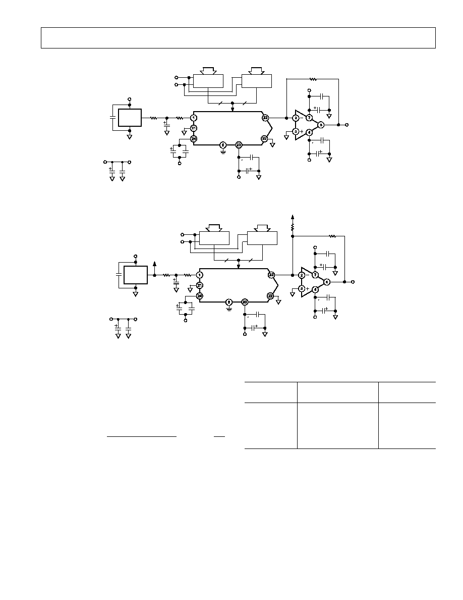
This SHA circuit uses the inverting integrator structure. A
300 MHz gain-bandwidth product op amp, the AD841, is the
heart of this fast SHA. The time constant formed by the 200
resistor and the 100 pF capacitor determines the acquisition
time and also hand limits the output signal to eliminate slew-
induced distortion.
DAC16 Noise Performance
The novel architecture employed in the DAC16 yields very low
wideband noise. Figure 26 illustrates the circuit configuration
for evaluating the DAC16's noise performance. An OP27 is
used as the DAC16's output I�V converter which is configured
to produce a 5 V full-scale output voltage. The output of the
OP27 was then capacitively coupled to an OP37 stage config-
ured in a gain of 101. Note that the techniques for reducing
wideband noise of the voltage reference and the DAC's internal
reference amplifier were used. As a result of these techniques,
the DAC16 exhibited a full-scale output noise spectral density
of 31 pA/
Hz at 1 kHz.
Digital Feedthrough and Data Skew
The DAC16 features a compound DAC architecture where the
5 most significant bits utilize 31 identical, segmented current
sources to obtain optimal high speed settling at major code tran-
sitions. Although every effort has been made to equalize the
speeds at which the DAC switches operate, there exists finite
skew in the MSB DAC switches.
As with any converter product, a high speed digital-to-analog
converter is forced to exist on the frontier between the noisy en-
vironment of high speed digital logic and the sensitive analog
domain. The problems of this interlace are particularly acute
when demands of high speed (greater than 10 MHz switching
times) and high precision are combined. No amount of design
effort can perfectly isolate the analog portions of a DAC from
the spectral components of a digital input signal with a 2 ns rise
time. Inevitably, once this digital signal is brought onto the chip,
some of its higher frequency components will find their way to
the sensitive analog nodes, producing a digital feedthrough
glitch. To minimize the exposure to this effect, the DAC16 was
designed to omit intentionally the on-board latches that are usu-
ally included in many slower DACs. This not only reduces the
overall level of digital activity on chip, it also avoids bringing a
latch clock pulse onto the IC, whose opposite edge inevitably
produces a substantial glitch, even when the DAC is not sup-
posed to be changing codes.
The DAC16 uses each digital input line to switch each current
segment in the DAC between the output diode-connected
transistor and the logic control transistor. If the input bits are
not changed simultaneously, or if the different DAC bits switch
74AC11377
REF GND
R1
5k
I
REF
+15V
0.1 F
REF02
22 F
R2
5k
DAC16
C
COMP
C1
47 F
I
OUT
AGND
C2
100nF
CERAMIC
�15V
10 F
0.1 F
+5V
DIGITAL +5V
PIN 3, DAC16
OP27A
10 F
0.1 F
+15V
10 F
0.1 F
�15V
V
OUT
0V TO +5V FS
10 F
0.1 F
�15V
R3
1.25k
(2.49k
2)
8
8
CLK
EN
74AC11377
DB0 � DB7
DB8 � DB15
DIGITAL INPUT WORD
RESISTORS:
CADDOCK T912�5K�010�02 (OR EQUIVALENT)
5k , 0.01%, TC TRACK = 2 ppm/ C
Figure 26. DAC16 Noise Measurement Test Circuit
DAC16
REV. B
�11�
A discrete drive circuit is used to achieve the best performance
from the SD5000 quad DMOS switch. This switch-driving cell
is composed of MPS571 RF NPN transistors and an MC10124
TTL-to-ECL translator. Using this technique provides both
high speed and highly symmetrical drive signals for the SD5000
switches. The switches arc arranged in a single-pole, double-
throw (SPDT) configuration. The 500 pF "flyback" capacitor is
switched to the op amp summing junction during the hold mode
to keep switching transients from feeding to the output. This ca-
pacitor is grounded during sample mode to minimize its effect
on acquisition time.
Careful circuit layout of the high speed SHA section is almost as
important as the design itself. Double-sided printed circuit
board, a compact layout, and short critical signal paths all ensure
best performance.
Op Amp Selection
When selecting the amplifier to be used for the DAC16's I�V
converter, there are two main application areas; those requiring
high accuracy, and those seeking high speed. In high accuracy
applications, three parameters are of prime importance: (1)
input offset voltage. V
OS
; (2) input bias current, �I
B
; and (3) off-
set voltage drift, TCV
OS
. In these applications where 16-bit
performance must be maintained with an external reference
at +5 V, an op amp's input offset voltage must be less than 15
�
V
(
0.1 LSB) with a bias current less than 6 nA. The op amp
must also exhibit high open-loop gain to keep the offset voltage
below this limit over the specified full-scale output range. Thus,
for a maximum output of 5 V, the op amp's open loop gain
must be greater than 1300 V/mV.
For low frequency, high accuracy applications, Table IV lists
selected compatible operational amplifiers available from Analog
Devices. These operational amplifiers satisfy all the above
requirements and in most all cases will not require offset voltage
nulling.
Table V. Precision Operational Amplifier the DAC16
Model
V
OS
TCV
OS
I
B
A
VOL
OP177
10
�
V
0.3
�
V/
�
C
2 nA
12000 V/mV
OP77
25
�
V
0.6
�
V/
�
C
2.8 nA
2000 V/mV
OP27
25
�
V
0.3
�
V/
�
C
80 nA
1500 V/mV
OP97
25
�
V
2
�
V/
�
C
0.15 nA
2000 V/mV
In high speed applications where resolution is more important
than absolute accuracy, operational amplifiers such as the
AD843 offer the requisite settling time. Although these amplifi-
ers are not specified for 16-bit performance, their settling times
are two to three times faster than the DAC16 and will introduce
negligible error to the overall circuit's settling time. It is possible
to estimate the 16-bit settling time of an operational amplifier if
its 12-bit settling time is known. Assuming that the op amp can
be modeled by a single-pole response, then the ratio of the op
amp's 16-bit settling time to its 12-bit settling can be expressed
as:
t
s
(16
-
bit )
t
s
(12
-
bit )
=
1.33
Since many operational amplifier data sheets provide charts
illustrating 0.01% settling time versus output voltage step size,
all that is required to estimate an op amp's 16-bit settling time is
to multiply the 12-bit settling time for the required full-scale
voltage by 1.33. The circuit's overall settling time can then be
approximated by the root-sum-square method:
t
S
=
(
t
DAC
)
2
+
(
t
OA
)
2
where
t
DAC
=
DAC16's specified full-scale settling time
t
OA
= Op amp full-scale settling time
As a design aid, Table VI illustrates a high speed operational
amplifier selector guide for devices compatible with the DAC16
for high speed applications. All these devices exhibit the requi-
site settling time, input offset voltage, and input bias current
consistent with maximum performance.
Table VI. High Speed Operational Amplifiers for the DAC16
Model
t
S
to %
V
OS
TCV
OS
I
B
A
VOL
OP467 200 ns �0.01 0.5 mV
3.5
�
V/
�
C 0.5
�
A
20 V/mV
AD817 70 ns �0.01
2 mV
10
�
V/
�
C 6.6
�
A
6 V/mV
AD829 90 ns �0.1
0.5 mV
0.3
�
V/
�
C 7
�
A
100 V/mV
AD841 110 ns �0.01 1 mV
35
�
V/
�
C 5
�
A
45 V/mV
AD843 135 ns �0.01 1 mV
12
�
V/
�
C 0.001
�
A 25 V/mV
AD845 350 ns �0.01 0.25 mV 5
�
V/
�
C
0.001
�
A 500 V/mV
AD847 120 ns �0.01 1 mV
15
�
V/
�
C 5
�
A
5.5 V/mV
AD841
6
8
5
100pF
M3
11
12
9
M2
3
4
1
M4
75
500pF
510
�15V
169
�5V
249
169
�5V
249
Q1
Q2
�5V
+5V
T/
H
14
13
16
M1
360
360
+15V
INPUT
IN4735
MC10124
200
OUTPUT
1.6k
0.39 F
20k
�15V
TO PIN 2
SD5000
Q1, Q2 = MPS571
M1 � M4 = SD5000
200
Figure 27. A High Performance Deglitching Circuit
DAC16
REV. B
�12�
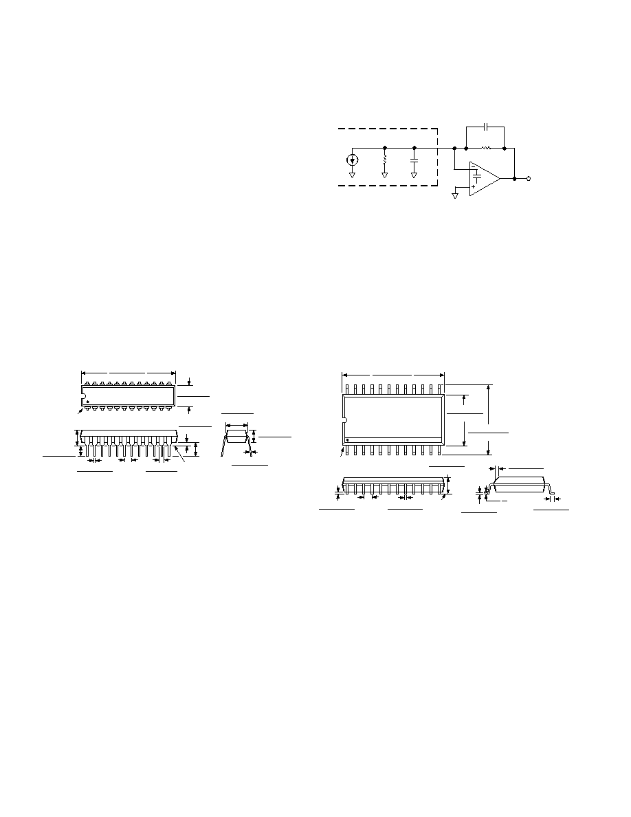
In using high speed op amps, the output capacitance of the
DAC16 appears across the inputs of the op amp where it and the
op amp's input capacitance will set an additional pole in the op
amp's loop gain response. The pole is formed with the feedback
resistance and the output resistance of the DAC. This additional
pole may adversely affect the transient response of the circuit
due to the added phase shift. Placing a small capacitor across the
feedback resistance, as shown in Figure 28, compensates for the
additional pole. The value of the capacitor can be determined by
setting R
FB
C
FB
= R
O
(C
O
+ C
IN
) and should be adjusted for opti-
mum transient response.
C1883b�1�4/99
PRINTED IN U.S.A.
OUTLINE DIMENSIONS
Dimensions shown in inches and (mm).
24-Lead Epoxy DIP (P)
(N-24)
24
1
12
13
PIN 1
1.275 (32.30)
1.125 (28.60)
0.280 (7.11)
0.240 (6.10)
0.195 (4.95)
0.115 (2.93)
0.015 (0.381)
0.008 (0.204)
0.325 (8.25)
0.300 (7.62)
SEATING
PLANE
0.060 (1.52)
0.015 (0.38)
0.210
(5.33)
MAX
0.022 (0.558)
0.014 (0.356)
0.200 (5.05)
0.125 (3.18)
0.150
(3.81)
MIN
0.100
(2.54)
BSC
0.070 (1.77)
0.045 (1.15)
24-Lead Epoxy SOL (S)
(R-24)
0.0125 (0.32)
0.0091 (0.23)
8
0
0.0291 (0.74)
0.0098 (0.25)
45
0.0500 (1.27)
0.0157 (0.40)
SEATING
PLANE
0.0118 (0.30)
0.0040 (0.10)
0.0192 (0.49)
0.0138 (0.35)
0.1043 (2.65)
0.0926 (2.35)
0.0500
(1.27)
BSC
24
13
12
1
0.4193 (10.65)
0.3937 (10.00)
0.2992 (7.60)
0.2914 (7.40)
PIN 1
0.6141 (15.60)
0.5985 (15.20)
The choice of amplifier depends entirely on the required system
accuracy, the required temperature range, and the operating
frequency.
I
DAC
R
O
C
O
R
FB
C
IN
C
FB
V
OUT
DAC16
Figure 28. Compensating for the Feedback Pole