 | –≠–ª–µ–∫—Ç—Ä–æ–Ω–Ω—ã–π –∫–æ–º–ø–æ–Ω–µ–Ω—Ç: DAC8043FS | –°–∫–∞—á–∞—Ç—å:  PDF PDF  ZIP ZIP |
REV. C
Information furnished by Analog Devices is believed to be accurate and
reliable. However, no responsibility is assumed by Analog Devices for its
use, nor for any infringements of patents or other rights of third parties
which may result from its use. No license is granted by implication or
otherwise under any patent or patent rights of Analog Devices.
a
12-Bit Serial Input
Multiplying CMOS D/A Converter
DAC8043
One Technology Way, P.O. Box 9106, Norwood, MA 02062-9106, U.S.A.
Tel: 617/329-4700
Fax: 617/326-8703
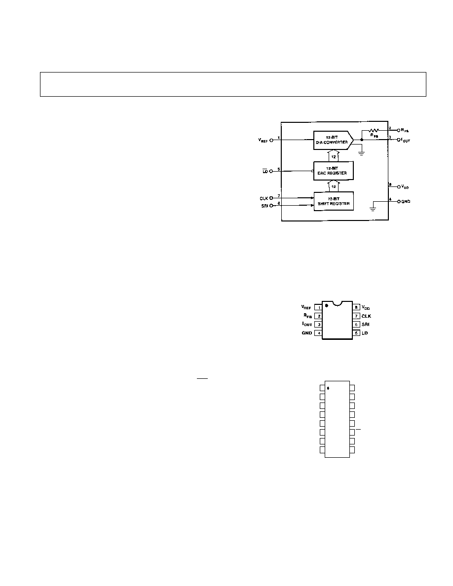
FUNCTIONAL BLOCK DIAGRAM
PIN CONNECTIONS
8-Pin Epoxy DIP
(P-Suffix)
8-Pin Cerdip
(Z-Suffix)
16-Lead Wide-Body SOL
(S-Suffix)
14
13
12
11
16
15
10
9
8
1
2
3
4
7
6
5
TOP VIEW
(Not to Scale)
DAC8043
NC = NO CONNECT
CLK
V
DD
N.C.
N.C.
N.C.
LD
SRI
N.C.
N.C.
N.C.
V
REF
R
FB
I
OUT
GND
GND
N.C.
GENERAL DESCRIPTION
The DAC8043 is a high accuracy 12-bit CMOS multiplying
DAC in a space-saving 8-pin mini-DIP package. Featuring serial
data input, double buffering, and excellent analog performance,
the DAC8043 is ideal for applications where PC board space is
at a premium. Also, improved linearity and gain error performance
permit reduced parts count through the elimination of trimming
components. Separate input clock and load DAC control lines
allow full user control of data loading and analog output.
The circuit consists of a 12-bit serial-in, parallel-out shift regis-
ter, a 12-bit DAC register, a 12-bit CMOS DAC, and control
logic. Serial data is clocked into the input register on the rising
edge of the CLOCK pulse. When the new data word has been
clocked in, it is loaded into the DAC register with the LD input
pin. Data in the DAC register is converted to an output current
by the D/A converter.
The DAC8043's fast interface timing may reduce timing design
considerations while minimizing microprocessor wait states. For
applications requiring an asynchronous CLEAR function or more
versatile microprocessor interface logic, refer to the PM-7543.
Operating from a single +5 V power supply, the DAC8043 is
the ideal low power, small size, high performance solution to
many application problems. It is available in plastic and cerdip
packages that are compatible with auto-insertion equipment.
FEATURES
12-Bit Accuracy in an 8-Pin Mini-DIP
Fast Serial Data Input
Double Data Buffers
Low 1/2 LSB Max INL and DNL
Max Gain Error: 1 LSB
Low 5 ppm/ C Max Tempco
ESD Resistant
Low Cost
Available in Die Form
APPLICATIONS
Autocalibration Systems
Process Control and Industrial Automation
Programmable Amplifiers and Attenuators
Digitally-Controlled Filters

REV. C
≠2≠
DAC8043≠SPECIFICATIONS
ELECTRICAL CHARACTERISTICS
DAC8043
Parameter
Symbol
Conditions
Min
Typ
Max
Units
STATIC ACCURACY
Resolution
N
12
Bits
Nonlinearity
INL
DAC8043A/E/G
±
1/2
LSB
(Note 1)
DAC8043F
1
LSB
Differential Nonlinearity
DNL
DAC8043A/E
±
1/2
LSB
(Note 2)
DAC8043F/G
±
1
LSB
Gain Error
G
FSE
T
A
= +25
∞
C
(Note 3)
DAC8043A/E
1
LSB
DAC8043F/G
2
LSB
T
A
= Full Temperature Range
All Grades
2
LSB
Gain Tempco
(
Gain/
Temp)
TC
GFS
±
5
ppm/
∞
C
(Note 5)
Power Supply
Rejection Ratio
PSRR
V
DD
=
±
5%
±
0.0006
±
0.002
%/%
(
Gain/
V
DD
)
Output Leakage Current
I
LKG
T
A
= +25
∞
C
±
5
nA
(Note 4)
T
A
= Full Temperature Range
DAC8043A
±
100
nA
DAC8043E/F/G
±
25
nA
Zero Scale Error
I
ZSE
T
A
= +25
∞
C
0.03
LSB
(Notes 7, 12)
T
A
= Full Temperature Range
DAC8043A
0.61
LSB
DAC8043E/F/G
0.15
LSB
Input Resistance
(Note 8)
R
IN
7
11
15
k
AC PERFORMANCE
Output Current
Settling Time
t
S
T
A
= +25
∞
C
0.25
1
µ
s
(Notes 5, 6)
V
REF
= 0 V
Digital to Analog
I
OUT
Load = 100
Glitch Energy
Q
C
EXT
= 13 pF
2
20
nVs
(Note 5, 10)
DAC Register Loaded Alternately with
All 0s and All 1s
Feedthrough Error
V
REF
= 20 V p-p @ f = 10 kHz
(V
REF
to I
OUT
)
FT
Digital Input = 0000 0000 0000
0.7
1
mV p-p
(Note 5, 11)
T
A
= +25
∞
C
Total Harmonic Distortion
THD
V
REF
= 6 V rms @ 1 kHz
≠85
dB
(Note 5)
DAC Register Loaded with All 1s
Output Noise Voltage Density
e
n
10 Hz to 100 kHz between R
FB
and I
OUT
17
nV/
Hz
(Note 5, 13)
DIGITAL INPUTS
Digital Input
HIGH
V
IN
2.4
V
Digital Input
LOW
V
IL
0.8
V
Input Leakage Current
I
IL
V
IN
= 0 V to +5 V
±
1
µ
A
(Note 9)
Input Capacitance
C
IN
V
IN
= 0 V
8
pF
(Note 5, 11)
ANALOG OUTPUTS
Output Capacitance
C
OUT
Digital Inputs = V
IH
110
pF
(Note 5)
Digital Inputs = V
IL
80
pF
(@ V
DD
= +5 V; V
REF
= +10 V; I
OUT
= GND = 0 V; T
A
= Full Temperature Range
specified under Absolute Maximum Ratings unless otherwise noted).

DAC8043
Parameter
Symbol
Conditions
Min
Typ
Max
Units
TIMING CHARACTERISTICS (NOTES 5, 14)
Data Setup Time
t
DS
T
A
= Full Temperature Range
40
ns
Data Hold Time
t
DH
T
A
= Full Temperature Range
80
ns
Clock Pulse Width High
t
CH
T
A
= Full Temperature Range
90
ns
Clock Pulse Width Low
t
CL
T
A
= Full Temperature Range
120
ns
Load Pulse Width
t
LD
T
A
= Full Temperature Range
120
ns
LSB Clock Into Input Register
to Load DAC Register Time
t
ASB
T
A
= Full Temperature Range
0
ns
POWER SUPPLY
Supply Voltage
V
DD
4.75
5
5.25
V
Supply Current
I
DD
Digital Inputs = V
IH
or V
IL
500
µ
A max
Digital Inputs = 0 V or V
DD
100
µ
A max
≠3≠
REV. C
NOTES
1
1
±
1/2 LSB =
±
0.012% of full scale.
1
2
All grades are monotonic to 12-bits over temperature.
1
3
Using internal feedback resistor.
1
4
Applies to I
OUT
; All digital inputs = 0 V.
1
5
Guaranteed by design and not tested.
1
6
I
OUT
Load = 100
, C
EXT
= 13 pF, digital input = 0 V to V
DD
or V
DD
to 0 V. Extrapolated to 1/2 LSB; t
S
= propagation delay (t
PD
) + 9
where
= measured time
constant of the final RC decay.
1
7
V
REF
= +10 V, all digital inputs = 0 V.
1
8
Absolute temperature coefficient is less than +300 ppm/
∞
C.
1
9
Digital inputs are CMOS gates; I
IN
is typically 1 nA at +25
∞
C.
10
V
REF
= 0 V, all digital inputs = 0 V to V
DD
or V
DD
to 0 V.
11
All digit inputs = 0 V.
12
Calculated from worst case R
REF
: I
ZSE
(in LSBs) = (R
REF
◊
I
LKG
◊
4096)/V
REF
.
13
Calculations from en =
4K TRB
where: K = Boltzmann constant, J/
∞
K, R = resistance,
, T = resistor temperature,
∞
K, B = bandwidth, Hz.
14
Tested at V
IN
= 0 V or V
DD
.
Specifications subject to change without notice.
ABSOLUTE MAXIMUM RATINGS
(T
A
= +25
∞
C unless otherwise noted)
V
DD
to GND . . . . . . . . . . . . . . . . . . . . . . . . . . . . . . . . . .+17 V
V
REF
to GND . . . . . . . . . . . . . . . . . . . . . . . . . . . . . . . . . .
±
25 V
V
RFB
to GND . . . . . . . . . . . . . . . . . . . . . . . . . . . . . . . . . .
±
25 V
Digital Input Voltage Range . . . . . . . . . . . . . . . ≠0.3 V to V
DD
Output Voltage (Pin 3) . . . . . . . . . . . . . . . . . . . ≠0.3 V to V
DD
Operating Temperature Range
AZ Versions . . . . . . . . . . . . . . . . . . . . . . . . ≠55
∞
C to +125
∞
C
EZ/FZ/FP Versions . . . . . . . . . . . . . . . . . . . ≠40
∞
C to +85
∞
C
GP Version . . . . . . . . . . . . . . . . . . . . . . . . . . . . 0
∞
C to +70
∞
C
Junction Temperature . . . . . . . . . . . . . . . . . . . . . . . . . +150
∞
C
Storage Temperature . . . . . . . . . . . . . . . . . . . ≠65
∞
C to +150
∞
C
Lead Temperature (Soldering, 60 sec) . . . . . . . . . . . . . +300
∞
C
Package Type
JA
*
JC
Units
8-Pin Hermetic DIP (Z)
134
12
∞
C/W
8-Pin Plastic DIP (P)
96
37
∞
C/W
*
JA
is specified for worst case mounting conditions, i. e.,
JA
is specified for device
in socket for cerdip and P-DIP packages.
CAUTION
1. Do not apply voltages higher than V
DD
or less than GND po-
tential on any terminal except V
REF
(Pin 1) and R
FB
(Pin 2).
2. The digital control inputs are Zener-protected; however, per-
manent damage may occur on unprotected units from high
energy electrostatic fields. Keep units in conductive foam at
all times until ready to use.
3. Use proper antistatic handling procedures.
4. Absolute Maximum Ratings apply to both packaged devices
and DICE. Stresses above those listed under Absolute Maxi-
mum Ratings may cause permanent damage to the device.
ORDERING GUIDE
1
Relative
Temperature
Package
Model
Accuracy
Range
Option
DAC8043AZ
2
±
1/2 LSB
≠55
∞
C to +125
∞
C
8-Pin Cerdip
DAC8043AZ/883
2
±
1/2 LSB
≠55
∞
C to +125
∞
C
8-Pin Cerdip
DAC8043EZ
±
1/2 LSB
≠40
∞
C to +125
∞
C
8-Pin Cerdip
DAC8043FS
±
1 LSB
≠40
∞
C to +85
∞
C
16-Lead (Wide) SOL
DAC8043FZ
±
1 LSB
≠40
∞
C to +85
∞
C
8-Pin Cerdip
DAC8043FP
±
1 LSB
≠40
∞
C to +85
∞
C
8-Pin Epoxy DIP
DAC8043GP
±
1/2 LSB
0
∞
C to +70
∞
C
8-Pin Epoxy DIP
DAC8043HP
±
1 LSB
0
∞
C to +70
∞
C
8-Pin Epoxy DIP
NOTES
1
All commercial and industrial temperature range parts are available with burn-in.
2
For devices processed in total compliance to MIL-STD-883, add/883 after part
number. Consult factory for 883 data sheet.
DAC8043
DAC8043
≠4≠
REV. C
WAFER TEST LIMITS
@ V
DD
= +5 V, V
REF
= +10 V; I
OUT
= GND = 0 V, T
A
= +25 C.
DAC8043GBC
Parameter
Symbol
Conditions
Limit
Units
STATIC ACCURACY
Resolution
N
12
Bits min
Integral Nonlinearity
INL
±
1
LSB max
Differential Nonlinearity
DNL
±
1
LSB max
Gain Error
G
FSE
Using Internal Feedback Resistor
±
2
LSB max
Power Supply Rejection Ratio
PSRR
V
DD
=
±
5%
±
0.002
%/% max
Output Leakage Current (I
OUT
)
I
LKG
Digital Inputs = V
IL
±
5
nA max
REFERENCE INPUT
Input Resistance
R
IN
7/15
k
min/max
DIGITAL INPUTS
Digital Input HIGH
V
IH
2.4
V min
Digital Input LOW
V
IL
0.8
V max
Input Leakage Current
I
IL
V
IN
= 0 V to V
DD
±
1
µ
A max
POWER SUPPLY
Supply Current
I
DD
Digital Inputs = V
IN
or V
IL
500
µ
A max
Digital Inputs = 0 V or V
DD
100
µ
A max
NOTE
Electrical tests are performed at wafer probe to the limits shown. Due to variations in assembly methods and normal yield loss, yield after packaging is not guaranteed
for standard product dice. Consult factory to negotiate specifications based on dice lot qualifications through sample lot assembly and testing.
DICE CHARACTERISTICS
DIE SIZE 0.116
◊
0.109 inch, 12,644 sq. mils (2.95
◊
2.77 mm, 8.17 sq. mm)
1. V
REF
2. R
FB
3. I
OUT
4. GND
5. LD
6. SRI
7. CLK
8. V
DD
Substate (die backside) is internally connected to V
DD
.
WARNING!
ESD SENSITIVE DEVICE
CAUTION
ESD (electrostatic discharge) sensitive device. Electrostatic charges as high as 4000 V readily
accumulate on the human body and test equipment and can discharge without detection.
Although the DAC8043 features proprietary ESD protection circuitry, permanent damage may
occur on devices subjected to high energy electrostatic discharges. Therefore, proper ESD
precautions are recommended to avoid performance degradation or loss of functionality.
DAC8043
≠5≠
REV. C
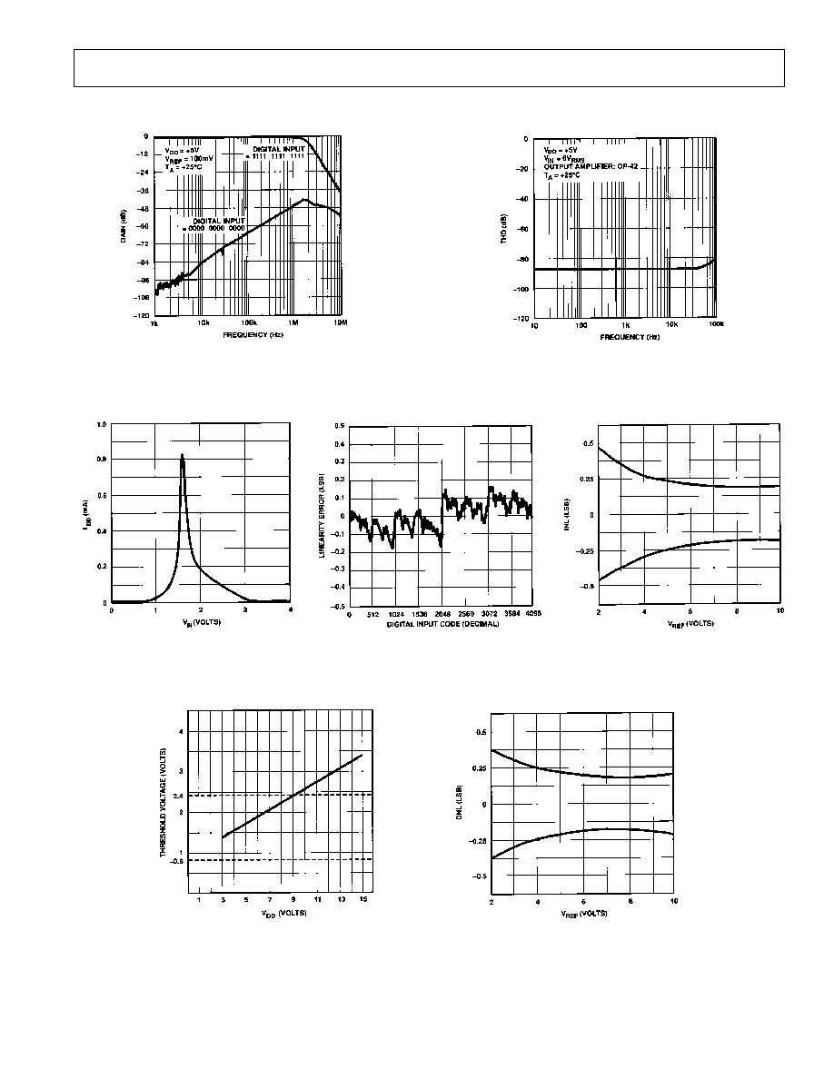
TYPICAL PERFORMANCE CHARACTERISTICS
Supply Current vs. Logic Input Voltage
Linearity Error vs. Digital Code
Linearity Error vs. Reference Voltage
Gain vs. Frequency (Output Amplifier: OP42)
Logic Threshold Voltage vs. Supply Voltage
Total Harmonic Distortion vs. Frequency
(Multiplying Mode)
DNL Error vs. Reference Voltage
DAC8043
≠6≠
REV. C
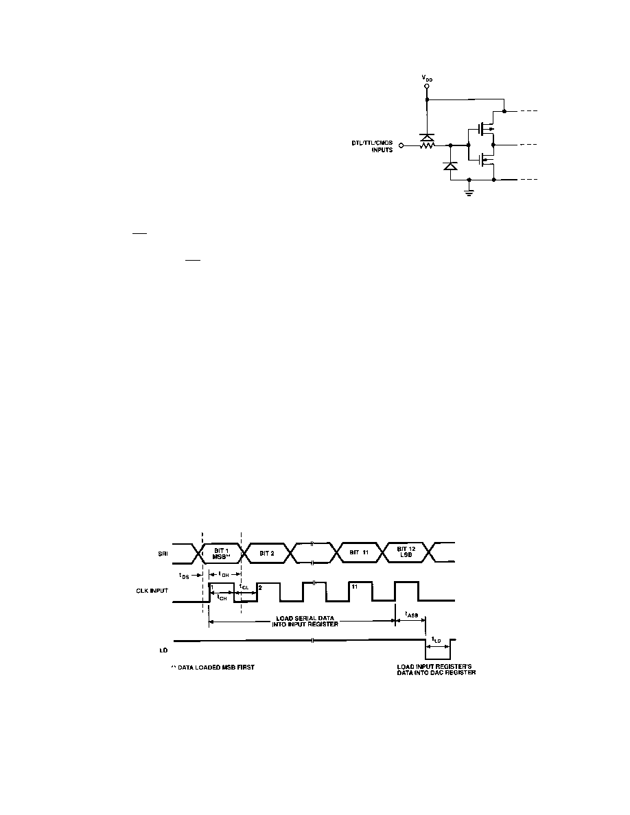
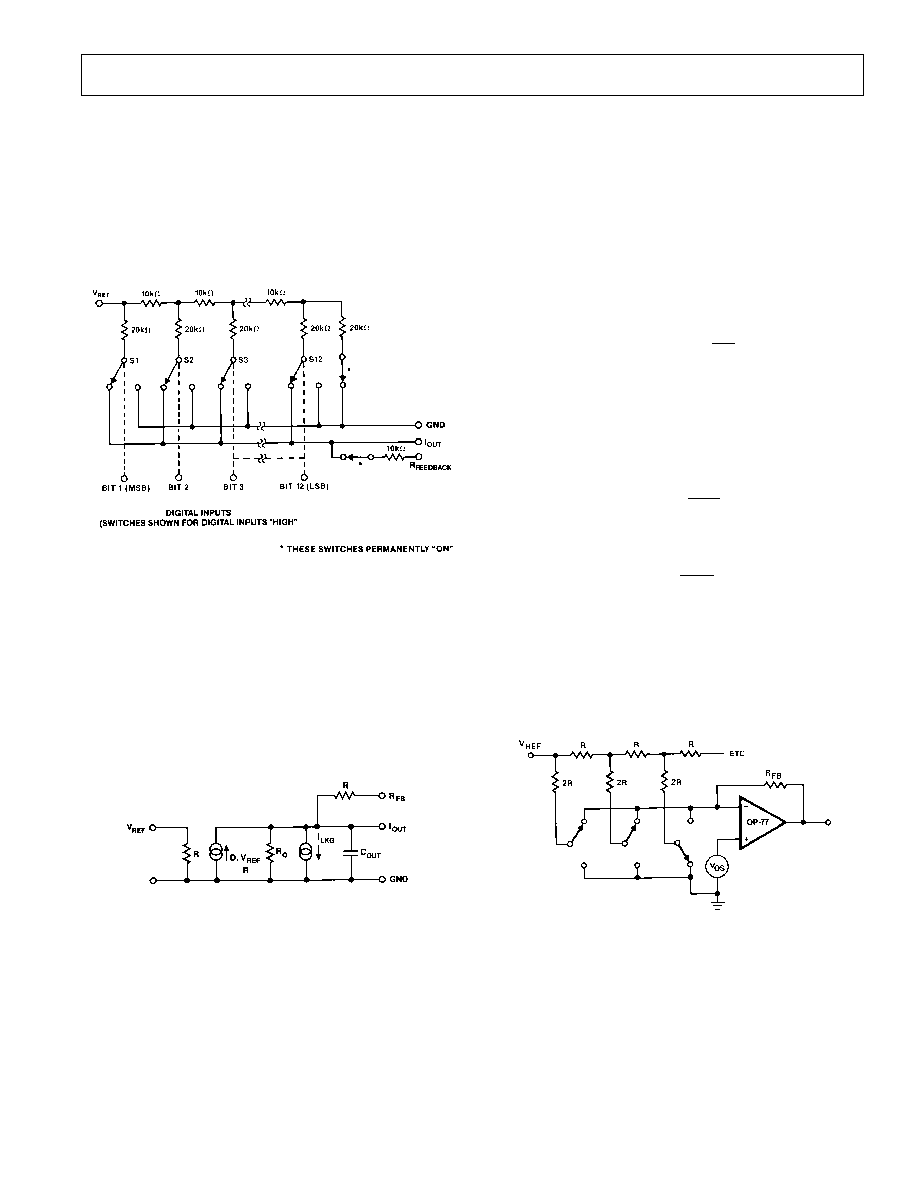
Figure 1. Digital Input Protection
The digital circuitry forms an interface in which serial data can
be loaded under microprocessor control into a 12-bit shift regis-
ter and then transferred, in parallel, to the 12-bit DAC register.
A simplified circuit of the DAC8043 is shown in Figure 2. An
inverted R-2R ladder network consisting of silicon-chrome,
highly-stable (+50 ppm/
∞
C) thin-film resistors, and twelve pairs
of NMOS current-steering switches.
These switches steer binarily weighted currents into either I
OUT
or GND; this yields a constant current in each ladder leg, regard-
less of digital input code. This constant current results in a con-
stant input resistance at V
REF
equal to R. The V
REF
input may
be driven by any reference voltage or current, ac or dc that is
within the limits stated in the Absolute Maximum Ratings.
The twelve output current-steering NMOS FET switches are in
series with each R-2R resistor, they can introduce bit errors if all
are of the same R
ON
resistance value. They were designed such
that the switch "ON" resistance be binarily scaled so that the
voltage drop across each switch remains constant. If, for ex-
ample, switch 1 of Figure 2 was designed with an "ON" resis-
tance of 10
, switch 2 for 20
, etc., a constant 5 mV drop will
then be maintained across each switch.
Write Cycle Timing Diagram
PARAMETER DEFINITIONS
INTEGRAL NONLINEARITY (INL)
This is the single most important DAC specification. ADI mea-
sures INL as the maximum deviation of the analog output (from
the ideal) from a straight line drawn between the end points. It
is expressed as a percent of full-scale range or in terms of LSBs.
Refer to PMI 1988 Data Book section 11 for additional digital-
to-analog converter definitions.
INTERFACE LOGIC INFORMATION
The DAC8043 has been designed for ease of operation. The
timing diagram illustrates the input register loading sequence.
Note that the most significant bit (MSB) is loaded first.
Once the input register is full, the data is transferred to the
DAC register by taking LD momentarily low.
DIGITAL SECTION
The DAC8043's digital inputs, SRI, LD, and CLK, are TTL
compatible. The input voltage levels affect the amount of cur-
rent drawn from the supply; peak supply current occurs as the
digital input (V
IN
) passes through the transition region. See the
Supply Current vs. Logic Input Voltage graph located under the
typical performance characteristics curves. Maintaining the digi-
tal input voltage levels as close as possible to the supplies, V
DD
and GND, minimizes supply current consumption.
The DAC8043's digital inputs have been designed with ESD re-
sistance incorporated through careful layout and the inclusion of
input protection circuitry. Figure 1 shows the input protection
diodes and series resistor; this input structure is duplicated on
each digital input. High voltage static charges applied to the in-
puts are shunted to the supply and ground rails through forward
biased diodes. These protection diodes were designed to clamp
the inputs to well below dangerous levels during static discharge
conditions.
GENERAL CIRCUIT INFORMATION
The DAC8043 is a 12-bit multiplying D/A converter with a very
low temperature coefficient. It contains an R-2R resistor ladder
network, data input and control logic, and two data registers.
DAC8043
≠7≠
REV. C
DYNAMIC PERFORMANCE
OUTPUT IMPEDANCE
The DAC8043's output resistance, as in the case of the output
capacitance, varies with the digital input code. This resistance,
looking back into the I
OUT
terminal, may be between 10 k
(the
feedback resistor alone when all digital inputs are LOW) and
7.5 k
(the feedback resistor in parallel with approximate 30 k
of the R-2R ladder network resistance when any single bit logic
is HIGH). Static accuracy and dynamic performance will be af-
fected by these variations.
This variation is best illustrated by using the circuit of Figure 4
and the equation:
V
ERROR
= V
OS
1
+
R
FB
R
O
where R
O
is a function of the digital code, and:
R
O
= 10 k
for more than four bits of logic 1.
R
O
= 30 k
for any single bit of logic 1.
Therefore, the offset gain varies as follows:
at code 0011 1111 1111,
V
ERROR1
= V
OS
1
+
10 k
10 k
= 2 V
OS
at code 0100 0000 0000,
V
ERROR2
= V
OS
1
+
10 k
30 k
= 4/3 V
OS
The error difference is 2/3 V
OS
.
Since one LSB has a weight (for V
REF
= +10 V) of 2.4 mV for
the DAC8043, it is clearly important that V
OS
be minimized,
either using the amplifier's nulling pins, an external nulling net-
work, or by selection of an amplifier with inherently low V
OS
.
Amplifiers with sufficiently low V
OS
include ADI's OP77, OP07,
OP27, and OP42.
Figure 4. Simplified Circuit
To further insure accuracy across the full temperature range,
permanently "ON" MOS switches were included in series with
the feedback resistor and the R-2R ladder's terminating resistor.
The "Simplified DAC Circuit," Figure 2, shows the location of
the series switches. These series switches are equivalently scaled
to two times switch 1 (MSB) and to switch 12 (LSB) respec-
tively to maintain constant relative voltage drops with varying
temperature. During any testing of the resistor ladder or
R
FEEDBACK
(such as incoming inspection), V
DD
must be present
to turn "ON" these series switches.
Figure 2. Simplified DAC Circuit
EQUIVALENT CIRCUIT ANALYSIS
Figure 3 shows an equivalent analog circuit for the DAC8043.
The (D
◊
V
REF
)/R current source is code dependent and is the
current generated by the DAC. The current source I
LKG
consists
of surface and junction leakages and doubles approximately ev-
ery 10
∞
C. C
OUT
is the output capacitance; it is the result of the
N-channel MOS switches and varies from 80 pF to 110 pF
depending on the digital input code. R
O
is the equivalent output
resistance that also varies with digital input code. R is the nomi-
nal R-2R resistor ladder resistance.
Figure 3. Equivalent Analog Circuit
DAC8043
≠8≠
REV. C
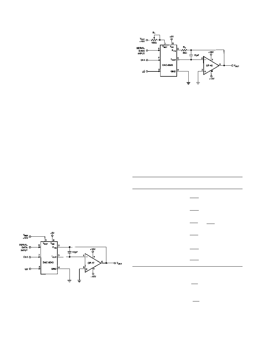
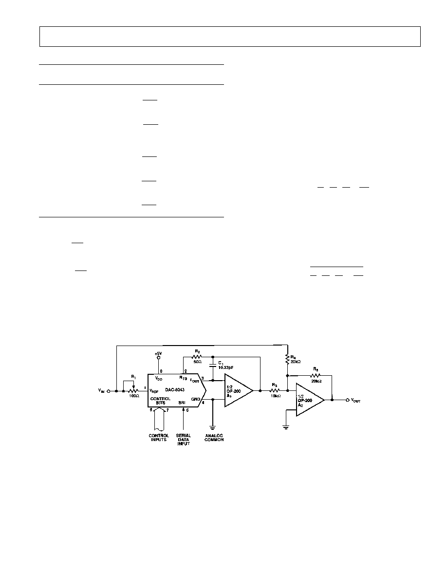
Figure 6. Unipolar Operation with Fast Op Amp and Gain
Error Trimming (2-Quadrant)
the analog output is shown in Table I. The limiting parameters
for the V
REF
range are the maximum input voltage range of the
op amp or
±
25 V, whichever is lowest.
Gain error may be trimmed by adjusting R
1
as shown in Figure
6. The DAC register must first be loaded with all 1s. R
1
may
then be adjusted until V
OUT
= ≠V
REF
(4095/4096). In the case of
an adjustable V
REF
, R
1
and R
2
may be omitted, with V
REF
ad-
justed to yield the desired full-scale output.
In most applications the DAC8043's negligible zero scale error
and very low gain error permit the elimination of the trimming
components (R
1
and the external R
2
) without adverse effects on
circuit performance.
The gain and phase stability of the output amplifier, board lay-
out, and power supply decoupling will all affect the dynamic
performance. The use of a small compensation capacitor may be
required when high-speed operational amplifiers are used. It
may be connected across the amplifier's feedback resistor to
provide the necessary phase compensation to critically damp the
output. The DAC8043's output capacitance and the R
FB
resis-
tor form a pole that must be outside the amplifier's unity gain
crossover frequency.
The considerations when using high-speed amplifiers are:
1. Phase compensation (see Figures 5 and 6).
2. Power supply decoupling at the device socket and use of
proper grounding techniques.
APPLICATIONS INFORMATION
APPLICATION TIPS
In most applications, linearity depends upon the potential of
I
OUT
and GND (pins 3 and 4) being exactly equal to each other.
In most applications, the DAC is connected to an external op
amp with its noninverting input tied to ground (see Figures 5
and 6). The amplifier selected should have a low input bias cur-
rent and low drift over temperature. The amplifier's input offset
voltage should be nulled to less than +200
µ
V (less than 10% of
1 LSB).
The operational amplifier's noninverting input should have a
minimum resistance connection to ground; the usual bias cur-
rent compensation resistor should not be used. This resistor can
cause a variable offset voltage appearing as a varying output er-
ror. All grounded pins should tie to a single common ground
point, avoiding ground loops. The V
DD
power supply should
have a low noise level with no transients greater than +17 V.
UNIPOLAR OPERATION (2-QUADRANT)
The circuit shown in Figures 5 and 6 may be used with an ac or
dc reference voltage. The circuit's output will range between 0 V
and approximately ≠V
REF
(4095/4096) depending upon the digital
input code. The relationship between the digital input and
Figure 5. Unipolar Operation with High Accuracy Op Amp
(2-Quadrant)
Table I. Unipolar Code Table
Digital Input
Nominal Analog Output
MSB
LSB
(V
OUT
as shown in Figures 5 and 6)
1111 1111 1111
≠V
REF
4095
4096
1000 0000 0001
≠V
REF
2049
4096
1000 0000 0000
≠V
REF
2048
4096
= ≠
V
REF
2
0111 1111 1111
≠V
REF
2047
4096
0000 0000 0001
≠V
REF
1
4096
0000 0000 0000
≠V
REF
0
4096
=
0
NOTES
1
Nominal full scale for the circuits of Figures 5 and 6 is given by
FS = ≠V
REF
4095
4096
2
Nominal LSB magnitude for the circuits of Figures 5 and 6 is given by
LSB = V
REF
1
4096
or V
REF
(2
≠n
).
DAC8043
≠9≠
REV. C
Table II. Bipolar (Offset Binary) Code Table
Digital Input
Nominal Analog Output
MSB
LSB
(V
OUT
as Shown in Figure 7)
1111 1111 1111
+V
REF
2047
2048
1000 0000 0001
+V
REF
1
2048
1000 0000 0000
0
0111 1111 1111
≠V
REF
1
2048
0000 0000 0001
≠V
REF
2047
2048
0000 0000 0000
≠V
REF
2048
2048
NOTES
1
Nominal full scale for the circuit of Figure 7 is given by
FS = V
REF
2047
2048
.
2
Nominal LSB magnitude for the circuit of Figure 7 is given by
LSB = V
REF
1
2048
.
Resistors R
3
, R
4
, and R
5
must be selected to match within 0.01%
and must all be of the same (preferably metal foil) type to assure
temperature coefficient matching. Mismatching between R
3
and
R
4
causes offset and full scale errors while an R
5
to R
4
and R
3
mismatch will result in full-scale error.
Calibration is performed by loading the DAC register with 1000
0000 0000 and adjusting R
1
until V
OUT
= 0 V. R
1
and R
2
may
be omitted, adjusting the ratio of R
3
to R
4
to yield V
OUT
= 0 V.
Full scale can be adjusted by loading the DAC register with
1111 1111 1111 and either adjusting the amplitude of V
REF
or
the value of R
5
until the desired V
OUT
is achieved.
ANALOG/DIGITAL DIVISION
The transfer function for the DAC8043 connected in the multi-
plying mode as shown in Figures 5, 6 and 7 is:
V
O
= ≠V
IN
A
1
2
1
+
A
2
2
2
+
A
3
2
3
+
...
A
12
2
12
where A
X
assumes a value of 1 for an "ON" bit and 0 for an
"OFF" bit.
The transfer function is modified when the DAC is connected in
the feedback of an operational amplifier as shown in Figure 8
and becomes:
V
O
=
≠V
IN
A
1
2
1
+
A
2
2
2
+
A
3
2
3
+
...
A
12
2
4
The above transfer function is the division of an analog voltage
(V
REF
) by a digital word. The amplifier goes to the rails with all
bits "OFF" since division by zero is infinity. With all bits "ON,"
the gain is 1 (
±
1 LSB). The gain becomes 4096 with the LSB,
bit 12 "ON."
Figure 7. Bipolar Operation (4-Quadrant, Offset Binary)
BIPOLAR OPERATION (4-QUADRANT)
Figure 7 details a suggested circuit for bipolar, or offset binary
operation. Table II shows the digital input to analog output re-
lationship. The circuit uses offset binary coding. Two's comple-
ment code can be converted to offset binary by software
inversion of the MSB or by the addition of an external inverter
to the MSB input.
DAC8043
≠10≠
REV. C
Figure 8. Analog/Digital Divider
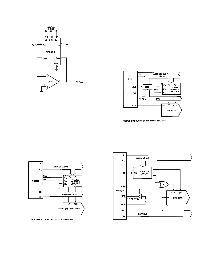
INTERFACING TO THE MC6800
As shown in Figure 9, the DAC8043 may be interfaced to the
6800 by successively executing memory WRITE instructions
while manipulating the data between WRITEs, so that each
WRITE presents the next bit.
In this example the most significant bits are found in memory
location 0000 and 0001. The four MSBs are found in the lower
half of 0000, the eight LSBs in 0001. The data is taken from the
DB
7
line.
The serial data loading is triggered by the CLK pulse which is
asserted by a decoded memory WRITE to memory location
2000, R/W, and
2. A WRITE to address 4000 transfers data
from input register to DAC register.
Figure 9. DAC8043≠MC6800 Interface
DAC8043 INTERFACE TO THE 8085
The DAC8043's interface to the 8085 microprocessor is shown
in Figure 10. Note that the microprocessor's SOD line is used
to present data serially to the DAC.
Data is clocked into the DAC8043 by executing memory write
instructions. The clock input is generated by decoding address
8000 and WR. Data is loaded into the DAC register with a
memory write instruction to address A000.
Serial data supplied to the DAC8043 must be present in the
right justified format in registers H and L of the microprocessor.
Figure 10. DAC8043-8085 Interface
DAC8043 TO 68000 INTERFACING
The DAC8043 interfacing to the 68000 microprocessor is
shown in Figure 11. Again, serial data to the DAC is taken from
one of the microprocessor's data bus lines.
Figure 11. DAC8043≠68000
µ
P Interface

≠11≠

000000000
PRINTED IN U.S.A.
≠12≠