 | –≠–ª–µ–∫—Ç—Ä–æ–Ω–Ω—ã–π –∫–æ–º–ø–æ–Ω–µ–Ω—Ç: DAC8248GP | –°–∫–∞—á–∞—Ç—å:  PDF PDF  ZIP ZIP |
REV. B
Information furnished by Analog Devices is believed to be accurate and
reliable. However, no responsibility is assumed by Analog Devices for its
use, nor for any infringements of patents or other rights of third parties
which may result from its use. No license is granted by implication or
otherwise under any patent or patent rights of Analog Devices.
a
Dual 12-Bit (8-Bit Byte)
Double-Buffered CMOS D/A Converter
DAC8248
One Technology Way, P.O. Box 9106, Norwood, MA 02062-9106, U.S.A.
Tel: 617/329-4700
Fax: 617/326-8703
FEATURES
Two Matched 12-Bit DACs on One Chip
12-Bit Resolution with an 8-Bit Data Bus
Direct Interface with 8-Bit Microprocessors
Double-Buffered Digital Inputs
RESET to Zero Pin
12-Bit Endpoint Linearity ( 1/2 LSB) Over Temperature
5 V to 15 V Single Supply Operation
Latch-Up Resistant
Improved ESD Resistance
Packaged in a Narrow 0.3" 24-Pin DIP and 0.3" 24-Pin
SOL Package
Available in Die Form
APPLICATIONS
Multichannel Microprocessor-Controlled Systems
Robotics/Process Control/Automation
Automatic Test Equipment
Programmable Attenuator, Power Supplies, Window
Comparators
Instrumentation Equipment
Battery Operated Equipment
GENERAL DESCRIPTION
The DAC8248 is a dual 12-bit, double-buffered, CMOS digital-
to-analog converter. It has an 8-bit wide input data port that inter-
faces directly with 8-bit microprocessors. It loads a 12-bit word in
two bytes using a single control; it can accept either a least signifi-
cant byte or most significant byte first. For designs with a 12-bit or
16-bit wide data path, choose the DAC8222 or DAC8221.
The DAC8248's double-buffered digital inputs allow both
DAC's analog output to be updated simultaneously. This is par-
ticularly useful in multiple DAC systems where a common
LDAC
signal updates all DACs at the same time. A single
RESET
pin resets both outputs to zero.
The DAC8248's monolithic construction offers excellent DAC-
to-DAC matching and tracking over the full operating tempera-
ture range. The DAC consists of two thin-film R-2R resistor
ladder networks, two 12-bit, two 8-bit, and two 4-bit data regis-
ters, and control logic circuitry. Separate reference input and
feedback resistors are provided for each DAC. The DAC8248
(continued on page 4)
FUNCTIONAL BLOCK DIAGRAM
PIN CONNECTIONS
24-Pin 0.3" Cerdip (W Suffix),
24-Pin Epoxy DIP (P Suffix),
24-Pin SOL (S Suffix)
DAC8248
Parameter
Symbol
Conditions
Min
Typ
Max
Units
STATIC ACCURACY
Resolution
N
12
Bits
Relative Accuracy
INL
DAC8248A/E/G
±
1/2
LSB
DAC8248F/H
±
1
LSB
Differential Nonlinearity
DNL
All Grades are Guaranteed Monotonic
±
1
LSB
Full-Scale Gain Error
1
G
FSE
DAC8248A/E
±
1
LSB
DAC8248G
±
2
LSB
DAC8248F/H
±
4
LSB
Gain Temperature Coefficient
(
Gain/
Temperature)
TCG
FS
(Notes 2, 3)
±
2
±
5
ppm/
∞
C
All Digital Inputs = 0s
Output Leakage Current
I
LKG
T
A
= +25
∞
C
±
5
±
10
I
OUT A
(Pin 2), I
OUT B
(Pin 24)
T
A
= Full Temperature Range
±
50
nA
Input Resistance (V
REF A
,
REF B
)
R
REF
(Note 4)
8
11
15
k
Input Resistance Match
R
REF
R
REF
±
0.2
±
1
%
DIGITAL INPUTS
Digital Input High
V
INH
V
DD
= +5 V
2.4
V
V
DD
= +15 V
13.5
V
Digital Input Low
V
INL
V
DD
= +5 V
0.8
V
V
DD
= +15 V
1.5
V
Input Current (V
IN
= 0 V
T
A
= +25
∞
C
±
0.001
±
1
µ
A
or V
DD
and V
INL
or V
INH
)
I
IN
T
A
= Full Temperature Range
±
10
µ
A
Input Capacitance
C
IN
DB0≠DB11
10
pF
(Note 2)
WR
, LDAC, DAC A/DAC B,
LSB/MSB, RESET
15
pF
POWER SUPPLY
Supply Current
I
DD
Digital Inputs = V
INL
or V
INH
2
mA
Digital Inputs = 0 V or V
DD
10
100
µ
A
DC Power Supply Rejection Ratio
PSRR
V
DD
=
±
5%
(
Gain/
V
DD
)
0.002
%/%
AC PERFORMANCE CHARACTERISTICS
2
Propagation Delay
5, 6
t
PD
T
A
= +25
∞
C
350
ns
Output Current Setting Time
6, 7
t
S
T
A
= +25
∞
C
1
µ
s
Output Capacitance
C
O
Digital Inputs = All 0s
C
OUT A
, C
OUT B
90
pF
Digital Inputs = All 1s
C
OUT A
, C
OUT B
120
pF
AC Feedthrough at
FT
A
V
REF A
to I
OUT A
; V
REF A
= 20 V p-p
I
OUT A
or I
OUT B
f = 100 kHz; T
A
= +25
∞
C
≠70
dB
FT
B
V
REF B
to I
OUT B
; V
REF B
= 20 V p-p
f = 100 kHz; T
A
= +25
∞
C
≠70
dB
REV. B
≠2≠
DAC8248≠SPECIFICATIONS
ELECTRICAL CHARACTERlSTICS
(@ V
DD
= +5 V or +15 V; V
REF A
= V
REF B
= +10 V; V
OUTA
= V
OUT B
= 0 V; AGND = DGND = 0 V;
T
A
= Full Temp Range specified in Absolute Maximum Ratings; unless otherwise noted. Specifications apply for DAC A and DAC B.)
Parameter
Symbol
Conditions
DAC8248
Units
V
DD
= +5 V
V
DD
= +15 V
Switching Characteristics
+25 C
≠40 C to +85 C
≠55 C to +125 C
All Temps
(Notes 2, 8)
(Note 9)
(Note 10)
LSB
/MSB Select to
Write Set-Up Time
t
CBS
130
170
180
80
ns min
LSB
/MSB Select to
Write Hold Time
t
CBH
0
0
0
0
ns min
DAC Select to
Write Set-Up Time
t
AS
180
210
220
80
ns min
DAC Select to
Write Hold Time
t
AH
0
0
0
0
ns min
LDAC to
Write Set-Up Time
t
LS
120
150
160
80
ns min
LDAC to
Write Hold Time
t
LH
0
0
0
0
ns min
Data Valid to
Write Set-Up Time
t
DS
160
210
220
70
ns min
Data Valid to
Write Hold Time
t
DH
0
0
0
10
ns min
Write Pulse Width
t
WR
130
150
170
90
ns min
LDAC Pulse Width
t
LWD
100
110
130
60
ns min
Reset Pulse Width
t
RWD
80
90
90
60
ns min
NOTES
1
1
Measured using internal R
FB A
and R
FB B
. Both DAC digital inputs = 1111 1111 1111.
1
2
Guaranteed and not tested.
1
3
Gain TC is measured from +25
∞
C to T
MIN
or from +25
∞
C to T
MAX
.
1
4
Absolute Temperature Coefficient is approximately +50 ppm/
∞
C.
1
5
From 50% of digital input to 90% of final analog output current. V
REF A
= V
REF B
= +10 V; OUT A, OUT B load = 100
, C
EXT
= 13 pF.
1
6
WR
, LDAC = 0 V; DB0≠DB7 = 0 V to V
DD
or V
DD
to 0 V.
1
7
Settling time is measured from 50% of the digital input change to where the output settles within 1/2 LSB of full scale.
1
8
See Timing Diagram.
1
9
These limits apply for the commercial and industrial grade products.
10
These limits also apply as typical values for V
DD
= +12 V with +5 V CMOS logic levels and T
A
= +25
∞
C.
Specifications subject to change without notice.
Burn-In Circuit
DAC8248
≠3≠
REV. B
DAC8248
≠4≠
REV. B
ORDERING GUIDE
1
Relative
Accuracy
Gain Error
Temperature
Package
Model
(+5 V or +15 V)
(+5 V or +15 V)
Range
Description
DAC8248AW
2
±
1/2 LSB
±
1 LSB
≠55
∞
C to +125
∞
C
24-Pin Cerdip
DAC8248EW
±
1/2 LSB
±
1 LSB
≠40
∞
C to +85
∞
C
24-Pin Cerdip
DAC8248GP
±
1/2 LSB
±
2 LSB
0
∞
C to +70
∞
C
24-Pin Plastic DIP
DAC8248FW
±
1 LSB
±
4 LSB
≠40
∞
C to +85
∞
C
24-Pin Cerdip
DAC8248HP
±
1 LSB
±
4 LSB
0
∞
C to +70
∞
C
24-Pin Plastic DIP
DAC8248FP
±
1 LSB
±
4 LSB
≠40
∞
C to +85
∞
C
24-Pin Plastic DIP
DAC8248HS
3
±
1 LSB
±
4 LSB
0
∞
C to +70
∞
C
24-Pin SOL
NOTES
1
Burn-in is available on commercial and industrial temperature range parts in cerdip, plastic DIP, and TO-can packages.
2
For devices processed in total compliance to MIL-STD-883, add/883 after part number. Consult factory for 883 data sheet.
3
For availability and burn-in information on SO and PLCC packages, contact your local sales office.
(continued from page 1)
operates on a single supply from +5 V to +15 V, and it dissi-
pates less than 0.5 mW at +5 V (using zero or V
DD
logic levels).
The device is packaged in a space-saving 0.3", 24-pin DIP.
The DAC8248 is manufactured with PMI's highly stable thin-
film resistors on an advanced oxide-isolated, silicon-gate,
CMOS technology. PMI's improved latch-up resistant design
eliminates the need for external protective Schottky diodes.
ABSOLUTE MAXIMUM RATINGS
(T
A
= +25
∞
C, unless otherwise noted.)
V
DD
to AGND . . . . . . . . . . . . . . . . . . . . . . . . . . . . 0 V, +17 V
V
DD
to DGND . . . . . . . . . . . . . . . . . . . . . . . . . . . . 0 V, +17 V
AGND to DGND . . . . . . . . . . . . . . . . . . ≠0.3 V, V
DD
+0.3 V
Digital Input Voltage to DGND . . . . . . . ≠0.3 V, V
DD
+0.3 V
I
OUT A
, I
OUT B
to AGND . . . . . . . . . . . . . . ≠0.3 V, V
DD
+0.3 V
V
REF A
, V
REF B
to AGND . . . . . . . . . . . . . . . . . . . . . . . .
±
25 V
V
RFB A
, V
RFB B
to AGND . . . . . . . . . . . . . . . . . . . . . . . .
±
25 V
Operating Temperature Range
AW Version . . . . . . . . . . . . . . . . . . . . . . . ≠55
∞
C to +125
∞
C
EW, FW, FP Versions . . . . . . . . . . . . . . . . ≠40
∞
C to +85
∞
C
GP, HP, HS Versions . . . . . . . . . . . . . . . . . . . 0
∞
C to +70
∞
C
Junction Temperature . . . . . . . . . . . . . . . . . . . . . . . . +150
∞
C
Storage Temperature . . . . . . . . . . . . . . . . . . ≠65
∞
C to +150
∞
C
Lead Temperature (Soldering, 60 sec) . . . . . . . . . . . . +300
∞
C
Package Type
JA
1
JC
Units
24-Pin Hermetic DIP (W)
69
10
∞
C/W
24-Pin Plastic DIP (P)
62
32
∞
C/W
24-Pin SOL (S)
72
24
∞
C/W
NOTE
1
JA
specified for worst case mounting conditions, i.e.,
JA
is specified for device in
socket for cerdip and P-DIP packages;
JA
is specified for device soldered to printed
circuit board for SOL package.
CAUTION
1. Do not apply voltages higher than V
DD
or less than GND
potential on any terminal except V
REF
and R
FB
.
2. The digital control inputs are Zener-protected; however,
permanent damage may occur on unprotected units from
high energy electrostatic fields. Keep units in conductive
foam at all times until ready to use.
3. Do not insert this device into powered sockets; remove
power before insertion or removal.
4. Use proper antistatic handling procedures.
5. Devices can suffer permanent damage and/or reliability deg-
radation if stressed above the limits listed under Absolute
Maximum Ratings for extended periods. This is a stress rat-
ing only and functional operation at or above this specifica-
tion is not implied.
WARNING!
ESD SENSITIVE DEVICE
CAUTION
ESD (electrostatic discharge) sensitive device. Electrostatic charges as high as 4000 V readily
accumulate on the human body and test equipment and can discharge without detection.
Although the DAC8248 features proprietary ESD protection circuitry, permanent damage may
occur on devices subjected to high energy electrostatic discharges. Therefore, proper ESD
precautions are recommended to avoid performance degradation or loss of functionality.

DAC8248
≠5≠
REV. B
1
1. AGND
13. NC
1
2. I
OUTA
14. DB1
1
3. R
FB A
15. DB0(LSB)
1
4. V
REF A
16. RESET
1
5. DGND
17. LSB/MSB
1
6. DB7(MSB)
18. DAC A/DAC B
1
7. DB6
19. LDAC
1
8. DB5
20. WR
1
9. DB4
21. V
DD
10. DB3
22. V
REF B
11. DB2
23. R
FB B
12. NC
24. I
OUT B
SUBSTRATE (DIE BACKSIDE) IS INTERNALLY
CONNECTED TO V
DD
.
DICE CHARACTERISTICS
WAFER TEST LIMITS
@ V
DD
= +5 V or +15 V, V
REF A
= V
REF B
= +10 V, V
OUT A
= V
OUT B
= 0 V; AGND = DGND = 0 V; T
A
= 25 C.
DAC8248G
Parameter
Symbol
Conditions
Limit
Units
Relative Accuracy
INL
Endpoint Linearity Error
±
1
LSB max
Differential Nonlinearity
DNL
All Grades are Guaranteed Monotonic
±
1
LSB max
Full-Scale Gain Error
1
G
FSE
Digital Inputs = 1111 1111 1111
±
4
LSB max
Output Leakage
Digital Inputs = 0000 0000 0000
(I
OUT A
, I
OUT B
)
I
LKG
Pads 2 and 24
±
50
nA max
Input Resistance
(V
REF A
, V
REF B
)
R
REF
Pads 4 and 22
8/15
k
min/k
max
V
REF A
, V
REF B
Input
R
REF
Resistance Match
R
REF
±
1
% max
Digital Input High
V
INH
V
DD
= +5 V
2.4
V min
V
DD
= +15 V
13.5
V min
Digital Input Low
V
INL
V
DD
= +5 V
0.8
V max
V
DD
= +15 V
1.5
V max
Digital Input Current
I
IN
V
IN
= 0 V or V
DD
; V
INL
or V
INH
±
1
µ
A max
Supply Current
I
DD
All Digital Inputs V
INL
or V
INH
2
mA max
All Digital Inputs 0 V or V
DD
0.1
mA max
DC Supply Rejection
(
Gain/
V
DD
)
PSR
V
DD
=
±
5%
0.002
%/% max
NOTES
1
Measured using internal R
FB A
and R
FB B
.
Electrical tests are performed at wafer probe to the limits shown. Due to variations in assembly methods and normal yield loss, yield after packaging is not guaranteed
for standard product dice. Consult factory to negotiate specifications based on dice lot qualification through sample lot assembly and testing.
Die Size 0.124
◊
0.132 inch, 16,368 sq. mils
(3.15
◊
3.55 mm, 10.56 sq. mm)
DAC8248
≠6≠
REV. B
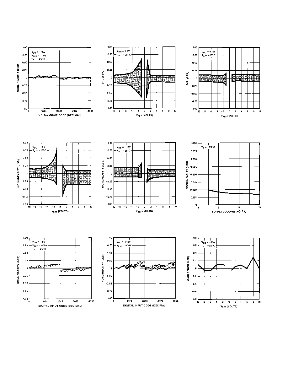
Channel-to-Channel Matching (DAC
A & B are Superimposed)
Nonlinearity vs. V
REF
Nonlinearity vs. Code (DAC A & B
are Superimposed)
Differential Nonlinearity vs. V
REF
Nonlinearity vs. V
REF
Nonlinearity vs. Code at T
A
= ≠55
∞
C,
+25
∞
C, +125
∞
C for DAC A & B
(All Superimposed)
Differential Nonlinearity vs. V
REF
Nonlinearity vs. V
DD
Absolute Gain Error Change vs. V
REF
≠Typical Performance Characteristics

DAC8248
≠7≠
REV. B
Full-Scale Gain Error vs. Temperature
Logic Input Threshold Voltage
vs. Supply Voltage (V
DD
)
Supply Current vs. Temperature
Supply Current vs. Logic Input Voltage
Multiplying Mode Frequency Response vs. Digital Code
Output Leakage Current vs. Temperature
Analog Crosstalk vs. Frequency

DAC8248
≠8≠
REV. B
Four Cycle Update
Five Cycle Update
Write Timing Cycle Diagram
PARAMETER DEFINITIONS
RESOLUTION (N)
The resolution of a DAC is the number of states (2
n
) that the
full-scale range (FSR) is divided (or resolved) into; where n is
equal to the number of bits.
RELATIVE ACCURACY (INL)
Relative accuracy, or integral nonlinearity, is the maximum de-
viation of the analog output (from the ideal) from a straight line
drawn between the end points. It is expressed in terms of least
significant bit (LSB), or as a percent of full scale.
DIFFERENTIAL NONLINEARITY (DNL)
Differential nonlinearity is the worst case deviation of any adja-
cent analog output from the ideal 1 LSB step size. The devia-
tion of the actual "step size" from the ideal step size of 1 LSB is
called the differential nonlinearity error or DNL. DACs with
DNL greater than
±
1 LSB may be nonmonotonic.
±
1/2 LSB
INL guarantees monotonicity and
±
1 LSB maximum DNL.
GAIN ERROR (G
FSE
)
Gain error is the difference between the actual and the ideal
analog output range, expressed as a percent of full-scale or in
terms of LSB value. It is the deviation in slope of the DAC
transfer characteristic from ideal.
Refer to PMI 1990/91 Data Book, Section 11, for additional
digital-to-analog converter definitions.
GENERAL CIRCUIT DESCRIPTION
CONVERTER SECTION
The DAC8248 incorporates two multiplying 12-bit current out-
put CMOS digital-to-analog converters on one monolithic chip.
It contains two highly stable thin-film R-2R resistor ladder net-
works, two 12-bit DAC registers, two 8-bit input registers, and
two 4-bit input registers. It also contains the DAC control logic
circuitry and 24 single-pole, double-throw NMOS transistor
current switches.
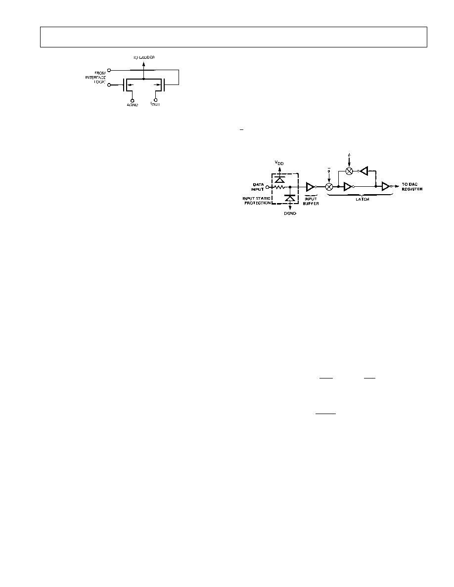
Figure 1 shows a simplified circuit for the R-2R ladder and tran-
sistor switches for a single DAC. R is typically 11 k
. The tran-
sistor switches are binarily scaled in size to maintain a constant
voltage drop across each switch. Figure 2 shows a single NMOS
transistor switch.
Figure 1. Simplified Single DAC Circuit Configuration.
(Switches Are Shown For All Digital Inputs at Zero)
DAC8248
≠9≠
REV. B
Figure 2. N-Channel Current Steering Switch
The binary-weighted currents are switched between I
OUT
and
AGND by the transistor switches. Selection between I
OUT
and
AGND is determined by the digital input code. It is important
to keep the voltage difference between I
OUT
and AGND termi-
nals as close to zero as practical to preserve data sheet limits. It
is easily accomplished by connecting the DAC's AGND to the
noninverting input of an operational amplifier and I
OUT
to the
inverting input. The amplifier's feedback resistor can be elimi-
nated by connecting the op amp's output directly to the DAC's
R
FB
terminal (by using the DAC's internal feedback resistor,
R
FB
). The amplifier also provides the current-to-voltage conver-
sion for the DAC's output current.
The output voltage is dependent on the DAC's digital input
code and V
REF
, and is given by:
V
OUT
= V
REF
◊
D/4096
where D is the digital input code integer number that is between
0 and 4095.
The DAC's input resistance, R
REF
, is always equal to a constant
value, R. This means that V
REF
can be driven by a reference
voltage or current, ac or dc (positive or negative). It is recom-
mended that a low temperature-coefficient external R
FB
resistor
be used if a current source is employed.
The DAC's output capacitance (C
OUT
) is code dependent and
varies from 90 pF (all digital inputs low) to 120 pF (all digital
inputs high).
To ensure accuracy over the full operating temperature range,
permanently turned "ON" MOS transistor switches were in-
cluded in series with the feedback resistor (R
FB
) and the R-2R
ladder's terminating resistor (see Figure 1). The gates of these
NMOS transistors are internally connected to V
DD
and will be
turned "OFF" (open) if V
DD
is not applied. If an op amp is us-
ing the DAC's R
FB
resistor to close its feedback loop, then V
DD
must be applied before or at the same time as the op amp's sup-
ply; this will prevent the op amp's output from becoming "open
circuited" and swinging to either rail. In addition, some applica-
tions require the DAC's ladder resistance to fall within a certain
range and are measured at incoming inspection; V
DD
must be
applied before these measurements can be made.
DIGITAL SECTION
The DAC8248's digital inputs are TTL compatible at V
DD
= +5 V
and CMOS compatible at V
DD
= +15 V. They were designed to
convert TTL and CMOS input logic levels into voltage levels that
will drive the internal circuitry. The DAC8248 can use +5 V
CMOS logic levels with V
DD
= +12 V; however, supply current
will increase to approximately 5 mA≠6 mA.
Figure 3 shows the DAC's digital input structure for one bit.
This circuitry drives the DAC registers. Digital controls,
and
, shown are generated from the DAC's input control logic
circuitry.
Figure 3. Digital Input Structure For One Bit
The digital inputs are electrostatic-discharge (ESD) protected
with two internal distributed diodes as shown in Figure 3; they
are connected between V
DD
and DGND. Each input has a typi-
cal input current of less than 1 nA.
The digital inputs are CMOS inverters and draw supply current
when operating in their linear region. Using a +5 V supply, the
linear region is between +1.2 V to +2.8 V with current peaking
at +1.8 V. Using a +15 V supply, the linear region is from
+1.2 V to +12 V (current peaking at +3.9 V). It is recom-
mended that the digital inputs be operated as close to the power
supply voltage and DGND as is practically possible; this will
keep supply currents to a minimum. The DAC8248 may be
operated with any supply voltage between the range of +5 V to
+15 V and still perform to data sheet limits.
The DAC8248's 8-bit wide data port loads a 12-bit word in two
bytes: 8-bits then 4-bits (or 4-bits first then 8-bits, at users dis-
cretion) in a right justified data format. This data is loaded into
the input registers with the LSB/MSB and WR control pins.
Data transfer from the input registers to the DAC registers can
be automatic. It can occur upon loading of the second data byte
into the input register, or can occur at a later time through a
strobed transfer using the LDAC control pin.
DAC8248
≠10≠
REV. B
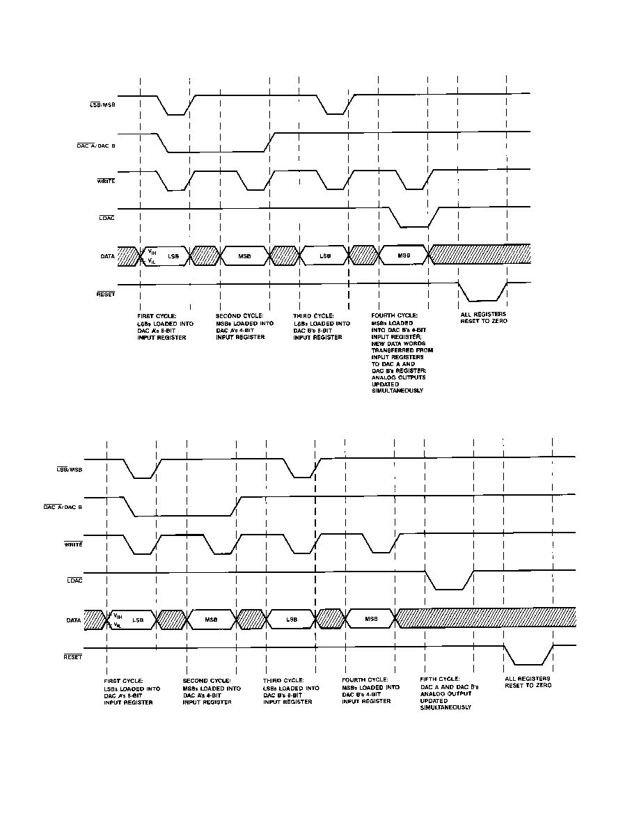
Figure 4. Four Cycle Update Timing Diagram
Figure 5. Five Cycle Update Timing Diagram
DAC8248
≠11≠
REV. B
AUTOMATIC DATA TRANSFER MODE
Data may be transferred automatically from the input register to
the DAC register. The first cycle loads the first data byte into
the input register; the second cycle loads the second data byte
and simultaneously transfers the full 12-bit data word to the
DAC register. It takes four cycles to load and transfer two com-
plete digital words for both DAC's, see Figure 4 (Four Cycle
Update Timing Diagram) and the Mode Selection Table.
STROBED DATA TRANSFER MODE
Strobed data transfer allows the full 12-bit digital word to be
loaded into the input registers and transferred to the DAC regis-
ters at a later time. This transfer mode requires five cycles: four
to load two new data words into both DACs, and the fifth to
transfer all data into the DAC registers. See Figure 5 (Five Cycle
Update Timing Diagram) and the Mode Selection Table.
Strobed data transfer separating data loading and transfer op-
erations serves two functions: the DAC output updating may be
more precisely controlled, and multiple DACs in a multiple
DAC system can be updated simultaneously.
RESET
The DAC8248 comes with a RESET pin that is useful in system
calibration cycles and/or during system power-up. All registers
are reset to zero when RESET is low, and latched at zero on the
rising edge of the RESET signal when WRITE is high.
INTERFACE CONTROL LOGIC
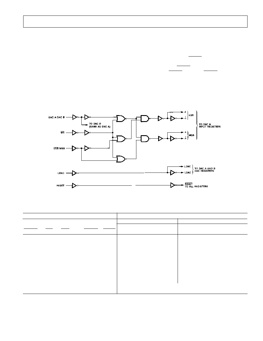
The DAC8248's control logic is shown in Figure 6. This cir-
cuitry interfaces with the system bus and controls the DAC
functions.
Figure 6. Input Control Logic
MODE SELECTION TABLE
DIGITAL INPUTS
REGISTER STATUS
DAC A
DAC B
Input Register
DAC
Input Register
DAC
DAC A/B
WR
LSB
/MSB
RESET
LDAC
LSB
MSB
Register
LSB
MSB
Register
L
L
L
H
H
WR
LAT
LAT
LAT
LAT
LAT
L
L
L
H
L
WR
LAT
WR
LAT
LAT
WR
L
L
H
H
H
LAT
WR
LAT
LAT
LAT
LAT
L
L
H
H
L
LAT
WR
WR
LAT
LAT
WR
H
L
L
H
H
LAT
LAT
LAT
WR
LAT
LAT
H
L
L
H
L
LAT
LAT
WR
WR
LAT
WR
H
L
H
H
H
LAT
LAT
LAT
LAT
WR
LAT
H
L
H
H
L
LAT
LAT
WR
LAT
WR
WR
X
H
X
H
H
LAT
LAT
LAT
LAT
LAT
LAT
X
H
X
H
L
LAT
LAT
WR
LAT
LAT
WR
X
X
X
L
X
ALL REGISTERS ARE RESET TO ZEROS
X
H
X
g
X
ZEROS ARE LATCHED IN ALL REGISTERS
L = Low, H = High, X = Don't Care, WR = Registers Being Loaded, LAT = Registers Latched.
DAC8248
≠12≠
REV. B
INTERFACE CONTROL LOGIC PIN FUNCTIONS
LSB
/MSB ≠ (PIN 17) LEAST SIGNIFICANT BIT (Active
Low)/ MOST SIGNIFICANT BIT (Active High). Selects
lower 8-bits (LSBs) or upper 4-bits (MSBs); either can be
loaded first. It is used with the WR signal to load data into the
input registers. Data is loaded in a right justified format.
DAC A
/DAC B ≠ (PIN 18) DAC SELECTION. Active low
for DAC A and Active High for DAC B.
WR
≠ (PIN 20) WRITE ≠ Active Low. Used with the LSB/
MSB signal to load data into the input registers, or Active High
to latch data into the input registers.
LDAC
≠ (PIN 19) LOAD DAC. Used to transfer data sim-
ultaneously from DAC A and DAC B input registers to both
DAC output registers. The DAC register becomes transparent
(activity on the digital inputs appear at the analog output) when
both WR and LDAC are low. Data is latched into the output
registers on the rising edge of LDAC.
RESET
≠ (PIN 16) ≠ Active Low. Functions as a zero over-
ride; all registers are forced to zero when the RESET signal is
low. All registers are latched to zeros when the write signal is
high and RESET goes high.
APPLICATIONS INFORMATION
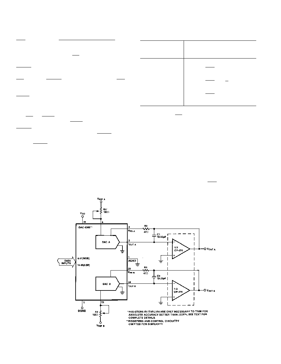
UNIPOLAR OPERATION
Figure 7 shows a simple unipolar (2-quadrant multiplication)
circuit using the DAC8248 and OP270 dual op amp (use two
OP42s for applications requiring higher speeds), and Table I
shows the corresponding code table. Resistors R1, R2, and R3,
R4 are used only if full-scale gain adjustments are required.
Table I. Unipolar Binary Code Table (Refer to Figure 7)
Binary Number in
DAC Register
Analog Output, V
OUT
MSB
LSB
(DAC A or DAC B)
1111 1111 1111
≠V
REF
4095
4096
1000 0000 0000
≠V
REF
2048
4096
= ≠
1
2
V
REF
0000 0000 0001
≠V
REF
1
4096
0000 0000 0000
0 V
NOTE
1 LSB = (2
-12
) (V
REF
)=
1
4096
(V
REF
)
Figure 7. Unipolar Configuration (2-Ouadrant Multiplication)
Low temperature-coefficient (approximately 50 ppm/
∞
C) resis-
tors or trimmers should be used. Maximum full-scale error
without these resistors for the top grade device and V
REF
=
±
10 V is 0.024%, and 0.049% for the low grade. Capacitors C1
and C2 provide phase compensation to reduce overshoot and
ringing when high-speed op amps are used.
Full-scale adjustment is achieved by loading the appropriate
DAC's digital inputs with 1111 1111 1111 and adjusting R1 (or
R3 for DAC B) so that:
V
OUT
= V
REF
◊
4095
4096
Full-scale can also be adjusted by varying V
REF
voltage and
eliminating R1, R2, R3, and R4. Zero adjustment is performed by
DAC8248
≠13≠
REV. B
loading the appropriate DAC's digital inputs with 0000 0000
0000 and adjusting the op amp's offset voltage to 0 V. It is rec-
ommended that the op amp offset voltage be adjusted to less
than 10% of 1 LSB (244
µ
V), and over the operating tempera-
ture range of interest. This will ensure the DAC's monotonicity
and minimize gain and linearity errors.
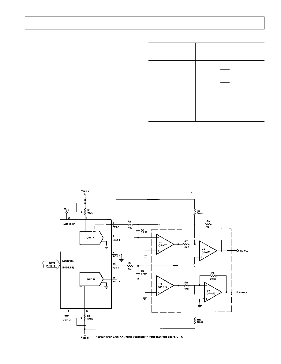
BIPOLAR OPERATION
The bipolar (offset binary) 4-quadrant configuration using the
DAC8248 is shown in Figure 8, and the corresponding code is
shown in Table II. The circuit makes use of the OP470, a quad
op amp (use four OP42s for applications requiring higher
speeds).
The full-scale output voltage may be adjusted by varying V
REF
or
the value of R5 and R8, and thus eliminating resistors R1, R2,
R3, and R4. If resistors R1 through R4 are omitted, then R5, R6,
R7 (R8, R9, and R10 for DAC B) should be ratio-matched to
0.01% to keep gain error within data sheet specifications. The re-
sistors should have identical temperature-coefficients if operating
over the full temperature range.
Zero and full-scale are adjusted in one of two ways and are at
the users discretion. Zero-output is adjusted by loading the ap-
propriate DAC's digital inputs with 1000 0000 0000 and vary-
ing R1 (R3 for DAC B) so that V
OUT A
(or V
OUT B
) equals 0 V.
If R1, R2 (R3, R4 for DAC B) are omitted, then zero output
can be adjusted by varying R6, R7 ratios (R9, R10 for DAC B).
Full-scale is adjusted by loading the appropriate DAC's digital
inputs with 1111 1111 1111 and varying R5 (R8 for DAC B).
Table II. Bipolar (Offset Binary) Code Table
(Refer to Figure 8)
Binary Number in
DAC Register
Analog Output, V
OUT
MSB
LSB
(DAC A or DAC B)
1111 1111 1111
+V
REF
2047
2048
1000 0000 0001
+V
REF
1
2048
1000 0000 0000
0 V
0111 1111 1111
≠V
REF
1
2048
0000 0000 0000
≠V
REF
2048
2048
NOTE:
1 LSB=(2
≠11
)(V
REF
) =
1
2048
(V
REF
)
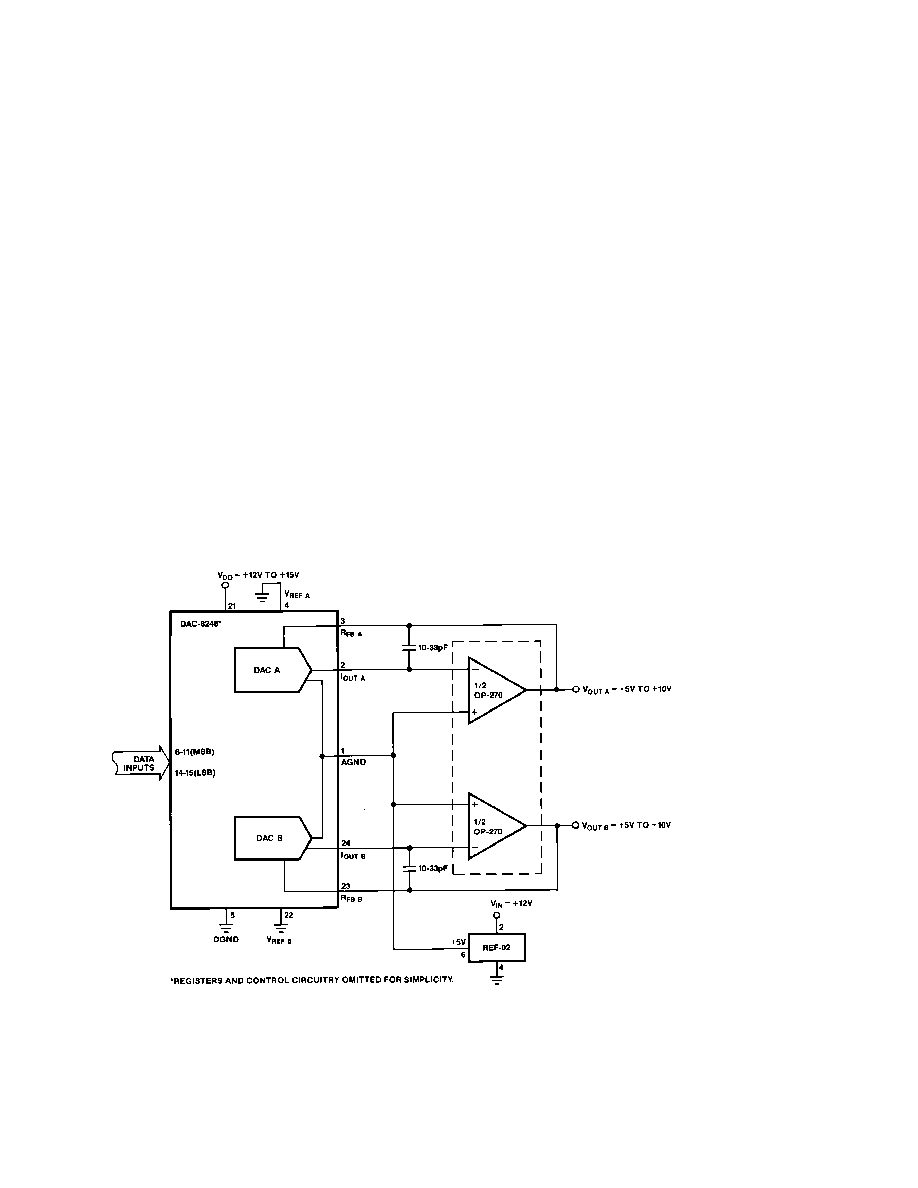
SINGLE SUPPLY OPERATION
CURRENT STEERING MODE
Because the DAC8248's R-2R resistor ladder terminating resis-
tor is internally connected to AGND, it lends itself well for
single supply operation in the current steering mode configura-
tion. This means that AGND can be raised above system
Figure 8. Bipolar Configuration (4-Quadrant Multiplication)
DAC8248
≠14≠
REV. B
ground as shown in Figure 9. The output voltage will be be-
tween +5 V and +10 V depending on the digital input code.
The output expression is given by:
V
OUT
= V
OS
◊
(D/4096)(V
OS
)
where V
OS
= Offset Reference Voltage (+5 V in Figure 9)
D = Decimal Equivalent of the Digital Input Word
VOLTAGE SWITCHING MODE
Figure 10 shows the DAC8248 in another single supply configu-
ration. The R-2R ladder is used in the voltage switching mode
and functions as a voltage divider. The output voltage (at the
V
REF
pin) exhibits a constant impedance R (typically 11 k
) and
must be buffered by an op amp. The R
FB
pins are not used and
are left open. The reference input voltage must be maintained
within +1.25 V of AGND, and V
DD
between +12 V and +15 V;
this ensures that device accuracy is preserved.
The output voltage expression is given by:
V
OUT
= V
REF
(D/4096)
where D = Decimal Equivalent of the Digital Input Word
APPLICATIONS TIPS
GENERAL GROUND MANAGEMENT
Grounding techniques should be tailored to each individual sys-
tem. Ground loops should be avoided, and ground current paths
should be as short as possible and have a low impedance.
The DAC8248's AGND and DGND pins should be tied to-
gether at the device socket to prevent digital transients from ap-
pearing at the analog output. This common point then becomes
the single ground point connection. AGND and DGND is then
brought out separately and tied to their respective power supply
grounds. Ground loops can be created if both grounds are tied
together at more than one location, i.e., tied together at the de-
vice and at the digital and analog power supplies.
PC board ground plane can be used for the single point ground
connection should the connections not be practical at the device
socket. If neither of these connections are practical or allowed,
then the device should be placed as close as possible to the sys-
tems single point ground connection. Back-to-back Schottky di-
odes should then be connected between AGND and DGND.
POWER SUPPLY DECOUPLING
Power supplies used with the DAC8248 should be well filtered
and regulated. Local supply decoupling consisting of a 1
µ
F to
10
µ
F tantalum capacitor in parallel with a 0.1
µ
F ceramic is
highly recommended. The capacitors should be connected be-
tween the V
DD
and DGND pins and at the device socket.
Figure 9. Single Supply Operation (Current Switching Mode)
DAC8248
≠15≠
REV. B
Figure 10. Single Supply Operation (Voltage Switching Mode)
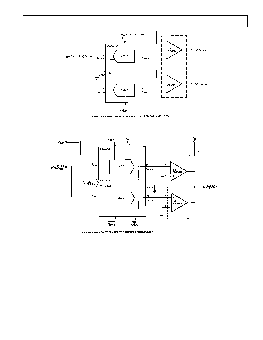
Figure 11. Digitally-Programmable Window Detector (Upper/Lower Limit Detector)
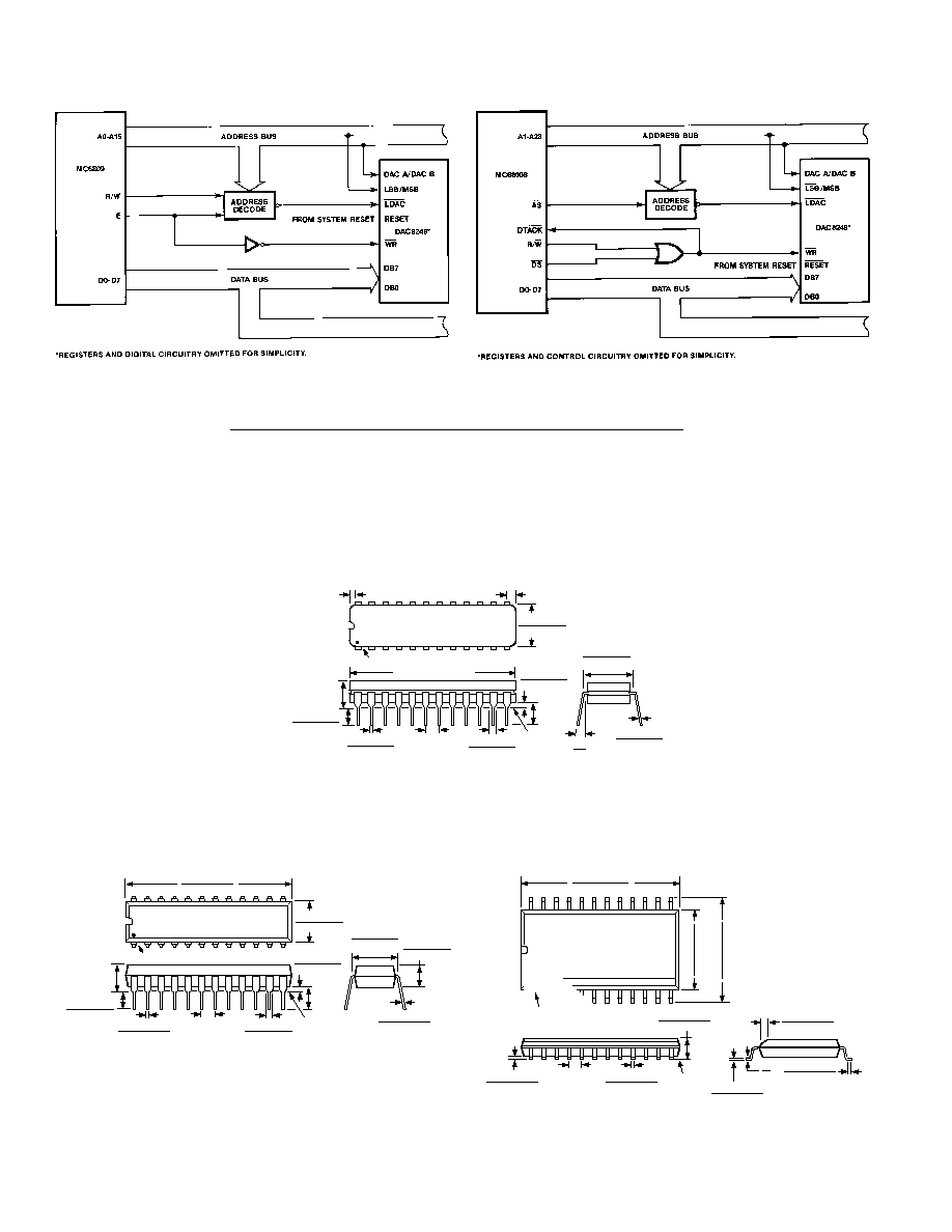
MICROPROCESSOR INTERFACE CIRCUITS
The DAC8248s versatile loading structure allows direct inter-
face to an 8-bit microprocessor. Its simplicity reduces the num-
ber of required glue logic components. Figures 12 and 13 show
the DAC8248 interface configurations with the MC6809 and
MC68008 microprocessors.
000000000
PRINTED IN U.S.A.
≠16≠
Figure 12. DAC8248 to MC6809 Interface
Figure 13. DAC8248 to MC68008 Interface
OUTLINE DIMENSIONS
Dimensions shown in inches and (mm).
24-Lead Cerdip
(Q-24)
24
1
12
13
0.310 (7.87)
0.220 (5.59)
PIN 1
0.005 (0.13) MIN
0.098 (2.49) MAX
SEATING
PLANE
0.023 (0.58)
0.014 (0.36)
0.200 (5.08)
MAX
1.280 (32.51) MAX
0.150
(3.81)
MIN
0.200 (5.08)
0.125 (3.18)
0.100 (2.54)
BSC
0.060 (1.52)
0.015 (0.38)
0.070 (1.78)
0.030 (0.76)
15
∞
0
∞
0.320 (8.13)
0.290 (7.37)
0.015 (0.38)
0.008 (0.20)
24 Lead SOL
(R-24)
24
13
12
1
0.6141 (15.60)
0.5985 (15.20)
0.4193 (10.65)
0.3937 (10.00)
0.2992 (7.60)
0.2914 (7.40)
PIN 1
SEATING
PLANE
0.0118 (0.30)
0.0040 (0.10)
0.0192 (0.49)
0.0138 (0.35)
0.1043 (2.65)
0.0926 (2.35)
0.0500
(1.27)
BSC
0.0125 (0.32)
0.0091 (0.23)
0.0500 (1.27)
0.0157 (0.40)
8
∞
0
∞
0.0291 (0.74)
0.0098 (0.25)
x 45
∞
24-Lead Plastic DIP
(N-24)
24
1
12
13
0.280 (7.11)
0.240 (6.10)
PIN 1
1.275 (32.30)
1.125 (28.60)
0.150
(3.81)
MIN
0.200 (5.05)
0.125 (3.18)
SEATING
PLANE
0.022 (0.558)
0.014 (0.356)
0.060 (1.52)
0.015 (0.38)
0.210
(5.33)
MAX
0.070 (1.77)
0.045 (1.15)
0.100 (2.54)
BSC
0.325 (8.25)
0.300 (7.62)
0.015 (0.381)
0.008 (0.204)
0.195 (4.95)
0.115 (2.93)