Äîêóìåíòàöèÿ è îïèñàíèÿ www.docs.chipfind.ru
One Technology Way, P.O. Box 9106, Norwood. MA 02062-9106, U.S.A.
Tel: 617/329-4700
Fax: 617/326-8703
REV. PrD
Information furnished by Analog Devices is believed to be accurate and
reliable. However, no responsibility is assumed by Analog Devices for
its use, nor for any infringements of patents or other rights of third parties
which may result from its use. No license is granted by implication or
otherwise under any patent or patent rights of Analog Devices.
=
FEATURES :
On-Board Reference, Oscillator, Control Logic and
Buffers
Easy interface to printer port of PC
PC Software for Control and Data Analysis
Stand Alone Capability to ease design
Analog and Digital Prototype Area
Preliminary Technical Data
Evaluation Board
AD1555/AD1556 24-Bit - ADC
EVAL-AD1555/56EB
GENERAL DESCRIPTION
The EVAL-AD1555/56EB is an evaluation board for the
AD1555 and AD1556 24-bit - ADC chip-set. The
AD1555/AD1556 chip-set can convert a high dynamic range
input signal, operates from +5V and -5V supplies and uses a
serial interface.
The AD1555/AD1556 evaluation board is designed to
demonstrate the ADC's performance and operation. A full
description of the AD1555/AD1556 is available in the
AD1555/AD1556 data sheet and should be consulted when
utilizing this evaluation board.
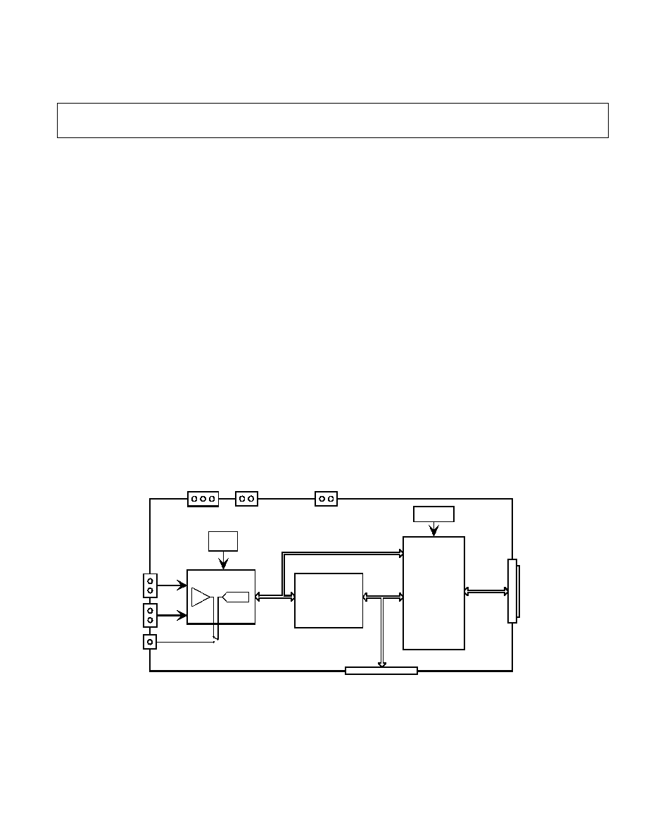
FUNCTIONAL BLOCK DIAGRAM
The EVAL-AD1555/56EB is ideal for use either as a stand-
alone evaluation board to interface with a customer applica-
tion or with any compatible PC using the parallel printer port.
On-board components include an AD780 3V ultra low noise
bandgap reference, a crystal oscillator, and digital control
logic. The board has both a Centronics male connector to
interface with PC printer port and a 50-pin connector for
stand-alone operation.
Software is provided to allow simple demonstration and
evaluation of the AD1555/AD1556 chip-set.
+5V
- 5V
S J3
oscillato r
AD 1555
AD 1556
Ref
FPG A
50-Way co nn ecto r
25-WAY D-T yp e
con nector
Ain
T in
+5V
S J2
+5V
S J1
mod
PGA
PG A_M O D
PRELIMINARY TECHNICAL DATA

2
REV. PrD
EVAL-AD1555/AD1556
OPERATING THE EVAL-AD1555/56EB
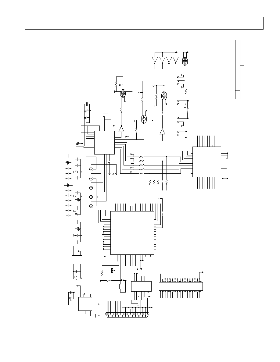
The EVAL-AD1555/56EB is a two-layer board carefully laid
out and tested to demonstrate the specific high dynamic
performance of the chip-set.
Figure 4 shows the schematics of the evaluation board.
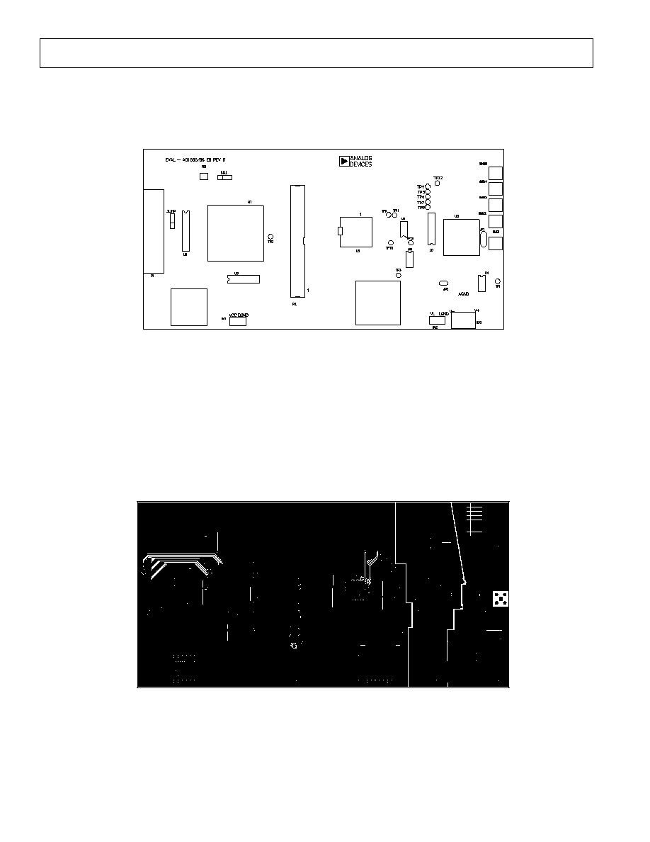
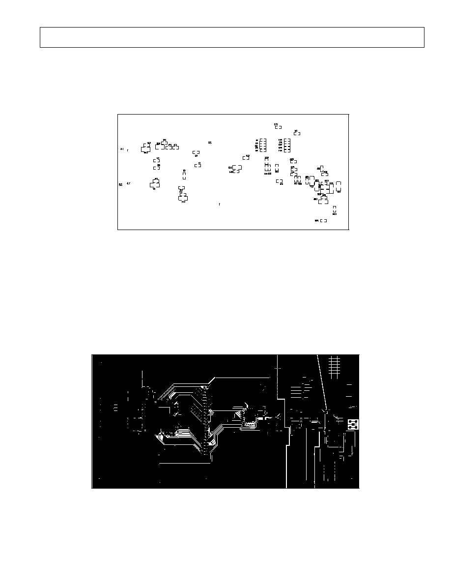
The layout of the board is given in the next four figures :
Figure 5 shows the Top side silk-screen.
Figure 6 shows the Top layer.
Figure 7 shows the Bottom side silk-screen.
Figure 8 shows the Bottom layer.
The available test points are listed in Table I and a description
of each selectable jumper is listed in Table II. The component
list is provided in Table III.
Power Supplies and Grounding :
The EVAL-AD1555/56EB has three power supply blocks: a
single +5V supply V
cc
(SJ1) for the evaluation board digital
section, another +5V or +3.3V supply V
L
(SJ2) for the digital
supply of AD1555 only and a +/-5V supply (SJ3) for the
analog section of AD1555.
The evaluation board ground plane is separated into three
sections: a DGND plane for the AD1556 and the digital
interface circuitry, a LGND plane for the digital section of
AD1555 and an analog AGND plane for the AD1555, its
analog input and external reference circuitry. To facilitate
grounding connections of test equipment and attain high
performance the board was designed with a good isolation
barrier between the AD1555 and the rest of the digital
functions. This isolation barrier is not required in applications
where the analog and digital ground are not tied together
externally. That is achieved using optocouplers and high
value resistors. The analog ground and AD1555 digital
ground can be tied together close to the AD1555 using JP2
which is the optimal configuration.
Analog inputs :
Fully differential signals could be applied on either A
IN
and
T
IN
inputs through SMB plugs. The analog input ranges have
to be compatible with the PGA gain settings used as described
in the AD1555/AD1556 datasheet. The modulator section of
the AD1555 can be separately evaluated using the
PGA_MOD SMB plug.
TABLE I. EVAL-AD1555/56EB Test Points
Test Point
Available Signal
TP1
REFIN (3V)
TP2
DGND ( FPGA )
TP3
DGND ( AD1556 )
TP4
CB0
TP5
CB1
TP6
CB2
TP7
CB3
TP8
CB4
TP9
MDATA
TP10
MCLKOUT
TP11
MFLG
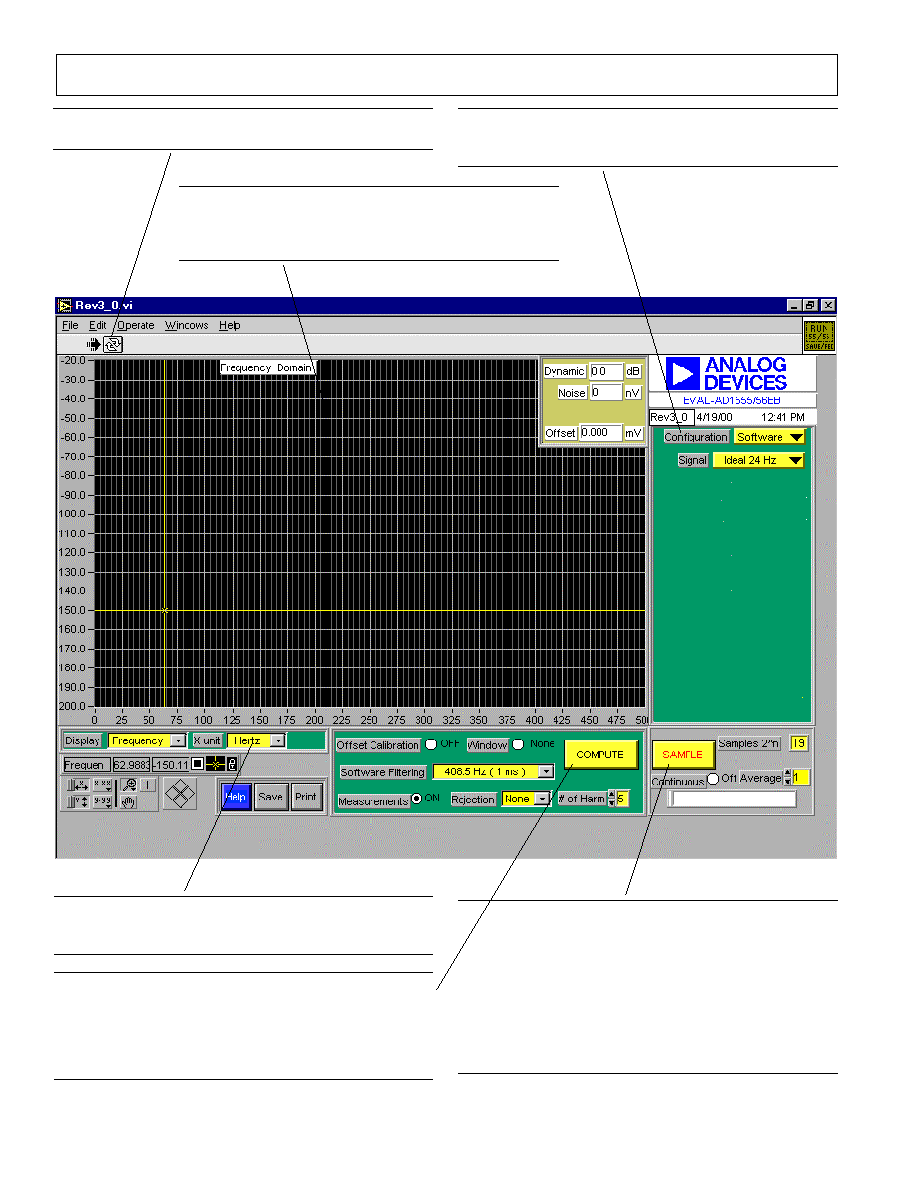
RUNNING THE EVAL-AD1555/56EB SOFTWARE
Software Description :
The EVAL-AD1555/56EB comes with software for analyzing
the AD1555/AD1556 chip-set. This software allows compre-
hensive control and evaluation of the AD1555/AD1556 chip-
set or the AD1555 and the AD1556 separately. The front-
end PC software has only one screen shown in Figure 1. This
screen is partitioned into five windows which allows the user
to select the configuration, launch the sampling sequence,
perform computation on the output signal and display the
results. The choices for display are Time domain response,
Spectral response and histogram chart. Different measure-
ments as Dynamic range, equivalent input noise, Total
Harmonic Distortion (THD) and DC offset can be done.
Figure 1 describes the steps to follow for proper software
operation.
Software Installation :
The EVAL-AD1555/56EB software runs under Windows95.
It requires a minimum of 7MB hard-disk space available and a
display with a minimum resolution of 800 by 600. Due to the
real-time operation, it is recommended that other programs
be closed when using the EVAL-AD1555/56EB software.
The EVAL-AD1555/56EB software installation process is:
- Run Setup.exe using the EVAL-AD1555/56EB disk 1 and
follow the instructions. The files can be stored in any direc-
tory at the user convenience using the destination folder field.
The default folder is C:\Program Files\Ad1555_56.
- Run AD1555_56.exe to launch the software. It will open
the window in figure 1.
- If the window in figure 1 exceeds the actual screen, the
display resolution needs to be increased by opening
Start>Settings>Control Panel>Display then settings>
800*600 for desktop area >apply>OK.
TABLE II. JUMPER DESCRIPTION
Jumper
Function
SW1
To get all the software functionality, SW1 should
be in the position where the identification dot on
the core of the switch is visible.
When SW1 is in the other position ( the switch
hole is hidden ), the AD1556 could be controlled
externally using the 50-pin connector P2. ( see
chapter using the EVAL-AD1555/56EB in
customized system for details ).
JP1
JP1 controls the input signal applied to the
AD1555 modulator input MODIN. In position A,
the PGA output is applied to MODIN. In
position B, the signal on PGA_MOD SMB plug is
applied to MODIN.
JP2
JP2 allows LGND and AGND to be tied together
close to the AD1555 which is generally the
preferred configuration.
PRELIMINARY TECHNICAL DATA

REV. PrD
3
EVAL-AD1555/AD1556
- The software uses a special font which can be installed using
Start>Settings>Control Panel>Fonts>File>install new fonts>
then select ADILogo Regular in the working directory then
OK.
- To operate the software, follow the 5 steps described in
figure 1.
Using the EVAL-AD1555/56B in the customized system :
The EVAL-AD1555/56EB is also designed to ease the
evaluation and the design of the AD1555 and the AD1556 in
the customized system. The useful interface signals can be
connected to the customized system using the connector P2.
The switch SW1 in the position where the identification dot
of the switch is hidden changes the configuration of U1 as
follows :
- The AD1556 CLKIN at 1.024MHz is supplied by U1 (
exact division by 8 of U5 oscillator ).
- U1 transmits the AD1556 MCLK output ( 256kHz ) to the
AD1555 MCLK with the appropriate phase ( one inversion
is done by U1 in order to cancel the U9 inversion).
- U1 output pins PGA0-4, CS*, R/W*, DINM1, BW0-2,
H/S*, RSEL, CSEL, PWRDN, RESET, SYNC, SCLKOUT,
TDATA are Hi-Z .
This configuration allows the control of these signals by the
customized system. The AD1555 and AD1556 clock are still
generated by the EVAL-AD1555/56EB.
Integrated Circuits
U1
FPGA EPM7128ELC84-15.
U2
AD1556AS.
U3
AD1555AP.
U4
reference AD780AN.
U5
Oscillator 8.192MHz.
U6
Buffer 74HC245.
U7
Invertor 74HC04.
U8,U9
Optocoupler HCPL2630.
Capacitors
C1-C6,C8-C9,C11-C12,
C14-C16,C22-C24,C27,
C29-C31,C33,C34
100nF Ceramic Capacitors.
C7,C10,C13,C17-C18,
C21,C25,C26,C28
10 F Tantalum Capacitors.
C20
22 F Tantalum Capacitor 6.3v.
TABLE III. Component List.
Resistors
R6,R10-R15
47.5K Resistor.
R1-R5
13K Resistor.
R8,R9
4.7K Resistor.
R17,R21,R22
2K Resistor.
R18-R20
402 Resistor.
R16
10 Resistor.
Sockets
P2
50pin Male ribbon cable connector.
P1
25pin DB-25 connector.
JP2
2 Position Male jumper strip.
PB1
SMT push-button.
SW1,JP1
Slide Switch.
SMB1-SMB5
SMB Connector.
PRELIMINARY TECHNICAL DATA
4
REV. PrD
EVAL-AD1555/AD1556
Step 2 Configuration menu: Selects Configuration, Signal
input, PGA gain setting, AD1556 filter selection, power
controls, interface settings.
Display window : displays either Time domain or Frequency
domain or Histogram and/or performance values such as
dynamic range, equivalent input noise level, THD and DC
offset.
Step 3 Sampling menu : after the desired samples number is
selected, SAMPLE launches a sampling sequence. When
complete, "Successful" will appear in the status window. If
not, verify the configuration and the hardware setup. When
the configuration or sampling menu is modified, a sampling
sequence should be done again. F2 is the key command for
"sample". "Continuous" allows continuous running sampling
and computing (F4 is the key command key for "continu-
ous"). "Average" allows the averaging between successive
sampling.
Step 4 Computation menu : COMPUTE launches the
specified computation data process before display, allowing
windowing, software filtering or measurements computation
if desired. Compute sequence should be done again after
changes into computation, sampling, configuration menus.
F3 is the key command for "compute".
Step 5 Display menu : selects Time/Frequency domain or
histogram, controls display parameters ( scales, zoom,
cursor...), and controls outputs ( save to file or print ).
Figure 1. Software main screen.
Step 1 Start execution: click on the double-arrows icon to
start execution.
PRELIMINARY TECHNICAL DATA
REV. PrD
5
EVAL-AD1555/AD1556
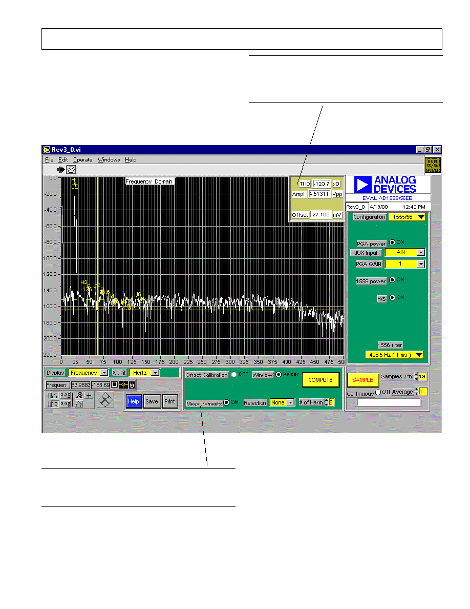
Figure 2. Frequency domain screen with measurements.
Measurement enable : This button enables the measure-
ments computation when on. 50 Hz or 60 Hz rejection filter
can be used before noise computation. The number of
harmonics uses in the THD computation is selectable.
Measurements display : This window displays the measure-
ments. When a signal approximately at least 10 times higher
than the noise floor is detected, the THD is measured
otherwise, the dynamic range and equivalent input noise are
displayed.
PRELIMINARY TECHNICAL DATA
6
REV. PrD
EVAL-AD1555/AD1556
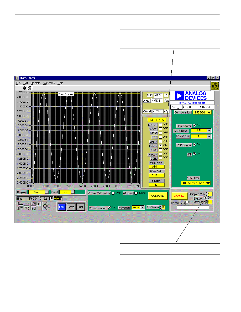
Figure 3. Time domain screen with AD1556 Status register content.
Status enable : This button enables the AD1556 Status
register reading. This feature is only available in time domain.
Status Register display : This window displays each bit of
the AD1556 status register. The displayed value is the status
register value corresponding to the data value marked with
the cursor in the time domain display.
PRELIMINARY TECHNICAL DATA
REV. PrD
7
EVAL-AD1555/AD1556
Figure 4. Schematics.
Title
Num
ber
Revision
Size
A
Date:
21-Feb-2002
Sheet of
File:
C:\A
NA
LO
G PRO
JE
CTS\A
D1555RE
VD
EVAL\AD1555R
EV
D.Ddb
Drawn By:
DGND
NC
46
N
C
6
I/O
40
NC
79
CSSW
RST
36
M
1M
0
37
RST
31
M
ANUAL
30
GND
82
CLKIN
83
M
CLKIN
65
DIN
33
SCLK
34
R/W
*LOAD
35
GLOBALCLEAR
1
N
C
39
GLOBALOE2
84
GLOBA
LOE1
2
DRDY
8
M
DATA
64
M
FLG
25
ERROR*
77
DOU
T
9
RSEL
81
CSEL
71
PW
RDN
75
TDATA
70
SYNC
69
RESET
76
H/S*
11
M
CLKOU
T
63
CLK56
67
O
UTEST
74
DINM
1
80
VCC
43
VCC
53
VCC
66
VCC
78
GND
7
GND
19
GND
32
GND
72
GND
59
GND
47
GND
42
VCC
3
VCC
13
VCC
26
VCC
38
PGA0
21
PGA1
20
PGA2
18
PGA3
17
PGA4
16
R/W
*
4
SCLKO
UT
10
CS*
5
BW
2
12
BW
1
14
BW
0
15
S3
50
I/O
73
I/O
41
I/O
51
I/O
52
I/O
54
I/O
55
I/O
56
I/O
57
I/O
58
I/O
60
I/O
61
I/O
62
I/O
68
I/O
22
I/O
23
I/O
24
I/O
27
I/O
29
I/O
28
S4
49
S5
48
S6
44
S7
45
U1
FPGA_84
C26
10uF
PB1
R8
4.7K
R9
4.7K
TP2
R3
13K
R2
13K
R1
13K
R5
13K
R4
13K
R6
47.5K
TP3
TP12
1
+5v
4
OUT
3
GND
2
U5
8.192M
Hz
C18
10uF
C23
.1uF
C21
10uF
C30
.1uF
C11
.1uF
C10
10uF
C15
.1uF
C27
.1uF
C28
10uF
C1
.1uF
C2
.1uF
C3
.1uF
C4
.1uF
C5
.1uF
C6
.1uF
C7
10uF
C8
.1uF
C9
.1uF
C14
.1uF
C12
.1uF
C13
10uF
C24
.1uF
C25
10uF
C34
.1uF
C16
.1uF
C22
.1uF
C17
10uF
C31
.1uF
C29
.1uF
VOUT
6
TRIM
5
GND
4
TEM
P
3
+VIN
2
N/C
1
N/C
7
2.5/3vSEL
8
U4
AD780
TP1
-VA
21
+VA
26
AGND2
27
AGND3
22
REFIN
25
AGND1
1
REFCAP2
24
REFCAP1
23
M
ODIN
28
PGAOUT
2
TIN-
8
TIN+
7
AIN-
6
AIN+
5
MCLK
18
MD
ATA
17
MFLG
15
CB4
14
CB3
13
CB2
12
CB1
11
CB0
10
LGND
16
-VA
20
VL
19
-VA
4
TEST
9
+VA
3
U3
AD1555
R18
402
B
A
R17
2K
1
2
U
7A
74HC04
1
2
3
JP1
TP8
TP7
TP6
TP5
TP4
TP13
C20
22uF
1
2
JP2
1
2
5
8
7
U8A
H
CPL2630
R22
2K
TP9
TP10
R19
402
R15
47.5K
AD1555 Evaluation Board
1
2
SJ1
VCC
11
VCC
22
VCC
44
DGND
12
DGND
23
DGND
24
DGND
34
M
DA
TA
36
TDATA
30
PW
RDN
26
CSEL
29
B
W
0
7
BW
1
8
BW
2
9
R
ESET
25
NC
28
RSEL
18
NC
27
H/S*
10
D
OUT
14
ERROR*
20
DRDY
15
DIN
19
SCLK
13
R/W
*
17
CS*
16
PGA4
6
PGA3
5
PGA
2
4
PGA
1
3
PG
A0
2
NC
1
NC
21
NC
33
CB0
43
CB1
42
CB2
41
CB3
40
CB4
39
MFLG
38
SYNC
31
CLKIN
32
MCLK
35
NC
37
U2
AD1556
R20
402
3
4
U
7B
74HC04
1
2
5
8
7
U9A
HCPL2630
11
10
U7E
74HC04
A
5
Y
6
U7C
74HC04
4
3
6
U9B
H
CPL2630
R10
47.5K
R11
47.5K
R12
47.5K
R13
47.5K
R14
47.5K
4
3
6
U8B
HCPL2630
9
8
U7D
74HC04
13
12
U7F
74HC04
R21
2K
TP11
1
2
SJ2
1
2
3
SJ3
2
1
R16
10
LGND
AGND
C33
.1uF
RGND
V-
V+
REFIN
SM
B2
AIN_P
SM
B3
AIN_N
SM
B4
TIN_P
SM
B5
TIN_N
DGND
VCC
VL
LGND
AGND
DGND
DG
ND
VCC
VCC
V+
V-
REFIN
V+
AGND
AGND
VCC
DGND
DGND
VCC
DGND
VCC
CB0
CB1
CB2
CB3
CB4
CS
R/W
*
SCLKOU
T
DINM
1
BW
2
BW
1
BW
0
HS
RSEL
RESET
CSEL
PW
RDN
SYNC
TDATA
M
CLKOUT
CLK
56
S3
S4
S5
S6
S7
C0
C1
C2
C3
TEST
CLKIN
M
CLKIN
D
RDY
DOUT
M
DATA
M
FLG
ERROR*
CLKIN
SW
1
1
14
2
15
3
16
4
17
5
18
6
19
7
20
8
21
9
22
10
23
11
24
12
25
13
P1
D
B25
C0
DIN
C1
A8
A8
DIN
SCLK
RW
LOAD
CSS
M
1M
0
RST
SCLK
C2
RW
LOAD
C3
CSS
M
1M
0
S3
S4
S5
S6
S7
DGND
A0
2
A1
3
A2
4
A3
5
A4
6
A5
7
A6
8
A7
9
B0
18
B1
17
B2
16
B3
15
B4
14
B5
13
B6
12
B7
11
E
19
D
IR
1
U6
74HC245
1
2
3
4
5
6
7
8
9
10
11
12
13
14
15
16
17
18
19
20
21
22
23
24
25
26
27
28
29
30
31
32
33
34
35
36
37
38
39
40
41
42
43
44
45
46
47
48
49
50
P2
H
EAD
ER 25X2
CB
0
CB
1
CB
2
CB3
CB4
BW
0
BW
1
BW
2
HS
SCLKOUT
DOU
T
DRDY
CS
R/W
*
RSEL
DINM
1
ERROR*
RESET
PW
RDN
TDATA
SYNC
CLK56
M
CLKOU
T
CSEL
M
CLKIN
M
FLG
M
DA
TA
TEST
LGND
V-
VL
CB0
CB1
CB2
CB3
CB4
M
FLG
SYNC
CLK56
M
CLKIN
CB0
CB
1
CB2
CB3
CB4
CS
R/W
*
SCLKOUT
D
IN
M
1
DRDY
ERR
OR*
DOU
T
DGN
D
VCC
M
DA
TA
TDATA
PW
RDN
CSEL
BW
0
BW
1
BW
2
RESET
RSEL
HS
M
DATA
VCC
VCC
DGND
VL
LGND
DGND
M
CLKOUT
LGND
LGND
M
FLG
LGND
D
GND
V
CC
VL
V+
V
-
DG
ND
LGN
D
AGN
D
M
CLK
C32
22uF
C19
22uF
RGND
SM
B1
PGA_M
ODE
RGND
AGND
AGND
D
G
ND
DGND
1
2
3
JUM
P
0277,
0277,
PRELIMINARY TECHNICAL DATA
8
REV. PrD
EVAL-AD1555/AD1556
Figure 6. Top layer ( not to scale).
Figure 5. Top side silk-screen ( not to scale).
PRELIMINARY TECHNICAL DATA
REV. PrD
9
EVAL-AD1555/AD1556
Figure 8. Bottom layer ( not to scale).
Figure 7. Bottom side silk-screen ( not to scale).
PRELIMINARY TECHNICAL DATA
Document Outline
- Features
- Product Description
- Functional Block Diagram
- Schematic
- OPERATING THE EVAL-AD1555/56EB
- RUNNING THE EVAL-AD1555/56EB SOFTWARE
- DIAGRAMS
- Software main screen.
- Frequency domain screen with measurements.
- Time domain screen with AD1556 Status register content.
- Top side silk-screen ( not to scale).
- Top layer ( not to scale).
- Bottom side silk-screen ( not to scale).
- Bottom layer ( not to scale).