Äîêóìåíòàöèÿ è îïèñàíèÿ www.docs.chipfind.ru
REV. 0
Information furnished by Analog Devices is believed to be accurate and
reliable. However, no responsibility is assumed by Analog Devices for its
use, nor for any infringements of patents or other rights of third parties
which may result from its use. No license is granted by implication or
a
EVAL-AD1852EB
One Technology Way, P.O. Box 9106, Norwood, MA 02062-9106, U.S.A.
Tel: 781/329-4700
World Wide Web Site: http://www.analog.com
Fax: 781/326-8703
© Analog Devices, Inc., 2001
24-Bit Stereo DAC
Evaluation Board
OVERVIEW
The EVAL-AD1852-EB evaluation board permits testing and
demonstrating the high-performance AD1852 24-bit stereo
DAC. An input signal is required in either optical or coaxial
SPDIF format or, alternatively, directly via a 10-pin header in
I
2
S, left justified, right justified, or DSP modes. A second 10-pin
header and DB-9 connector allows control of the internal regis-
ters from an external SPI controller.
Power requirements are a clean 9 V to 12 V dc source for the
digital section and a clean
±12 V dc for the analog section. The
positive supplies can be paralleled if desired. On-board regulators
derive separate "clean" 5 V dc supplies for the digital and analog
sections. Audio output is provided from two RCA phono jacks.
AD1852 OVERVIEW
The AD1852 is a complete 16-/20-/24-bit single-chip digital
audio, stereo digital-to-analog converter (DAC). It is comprised
of a multibit sigma-delta modulator with dither, continuous
time analog filters, and differential analog outputs. Other fea-
tures include an on-chip stereo attenuator, de-emphasis filter,
selectable interpolator and mute control, programmed through
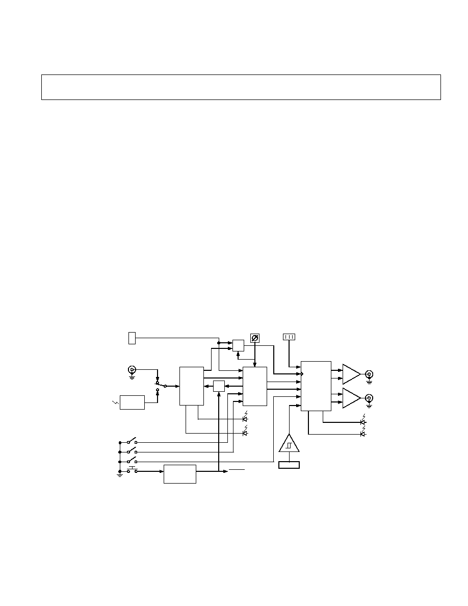
FUNCTIONAL BLOCK DIAGRAM
U4
I/F
MUX
U3
DAC
AD1852
U9B
U9A
DS1
ZERO LEFT
DS2
ZERO RIGHT
J6
LEFT
J7
RIGHT
JP1
INTERPOLATION
MODE
U5
J3/J5
SPI CONTROL
PORTS
U11
S5
INTERFACE
MODE
U10
U2
DIR
DS3
DEEMPH
DS4
VERF
S1
SIGNAL
SOURCE
SELECT
U1
TOS LINK
U8
RESET
GENERATOR
RESET
S6
RESET
S2
MUTE
S4
DEEMPHASIS
S3
SPDIF/EXT(J2)
J2 EXT DATA
J1 RCA JACK
OPTICAL
INPUT
SPDIF INPUT
an SPI-compatible serial control port. The AD1852 is fully
compatible with all known DVD formats including 96 kHz and
192 kHz sample rates and 24 bits. It also is backwards-compatible
by supporting 50
µs/15 µs digital de-emphasis intended for
"redbook" Compact Discs, as well as de-emphasis at 32 kHz
and 48 kHz sample frequencies.
The AD1852 has a very simple, but very flexible, serial data
input port that allows for a glueless interconnection to a variety
of ADCs, DSP chips, digital interface receivers (DIR) and
asynchronous sample rate converters (ASRC). The AD1852
can be configured in left-justified (LJ), I
2
S, right-justified (RJ),
or DSP serial port compatible modes. It can support 16, 20, and
24 bits in all modes. The AD1852 accepts serial audio data in
MSB first, twos complement format. A power-down mode is
offered to minimize power consumption when the device is
inactive. The AD1852 operates from a single 5 V power supply.
It is fabricated on a single monolithic integrated circuit and
housed in a 28-lead SSOP package. Normal operation over the
temperature range 0
°C to 70°C is guaranteed.
The AD1852 data sheet gives a more complete description of
operation.

REV. 0
EVAL-AD1852EB
2
FUNCTIONAL DESCRIPTION
The AD1852 evaluation board presents a reference design that
can be used as a suggested layout and circuit implementation,
which will deliver optimal performance from the audio DAC. As
far as is possible on an evaluation board, current assembly methods
and components are used. Most components are surface mount
devices and a four-layer printed circuit board is used with full
internal power and ground planes for best noise performance.
For guidance, a schematic, bill of materials, PLD source code,
and PCB plots are included in this document.
POWER SUPPLIES
The PC board is divided into analog and digital sections, each
with separate power supplies, to facilitate testing. The digital
power supply input is via binding post terminals J8 and J9. The
recommended digital supply is 12 V dc at 110 mA
± 25 mA. An
on-board voltage regulator (U6) provides 5 V dc,
± 5% to the
digital circuitry. The analog power supply inputs are binding
posts, J10, J11, and J12. Recommended analog supply is 12 V
dc at 50 mA
± 10 mA and 12 V dc at 20 ± 5 mA. An on-
board, low noise voltage regulator, (U7) provides 5 V dc,
±5%
to the analog power pins of the AD1852 DAC.
DIGITAL AUDIO SIGNAL INPUTS
RCA phone jack, (J1) and optical TOSLink input (U1) may be
used for standard SPDIF or AES/EBU input signals. J1 is termi-
nated with a 75
resistor. Switch S1 selects between J1 and U1
inputs and feeds the selected signal to the digital interface receiver
(U2). Switch SPDIF/EXT (S3) controls CPLD (U4) and U11,
which is used to switch signals between the SPDIF input (J1)
and the direct input, via the 10-pin header J2, EXT DATA
INTERFACE.
The EXT DATA INTERFACE input permits buffered (U4,
M464/32 and U11, HC00) access to the BCLK, L/
RCLK,
SDATA and MCLK inputs to the AD1852 DAC. This permits
testing with left-justified, I
2
S or right-justified, serial input modes.
Note that with right-justified input data, the AD1852 control
register must be programmed for the correct number of data
bits, i.e., 16, 20 or 24 bits. When using the direct input header,
it is necessary to provide all four signals, MCLK, BCLK, L/
RCLK
and SDATA. A termination network (RC1), consisting of a series
connected 100
resistor and a 47 pF capacitor, is shunted
across each signal line to reduce line reflections. A 10 k
pull-
up network (RT1) ensures the inputs are not floating in the
absence of an external data source.
EXTERNAL SPI CONTROL PORT
An external control port, SPI CONTROL PORT (J3), is pro-
vided, via a 10-pin header, so that the internal volume controls
and control registers can be programmed from an external host
or microcontroller. This port accepts serial data to indepen-
dently set the left/right volume or the operating mode of the
AD1852 by programming the contents of three internal 16-bit
registers. When setting the volume, a 16-bit control word has
14 bits allocated to the left or right volume control, giving a
total range of 84 dB. Details of the signal format and timing are
discussed in the AD1852 data sheet.
An additional connector, PC PORT (J5), has been provided to
permit connection to the parallel port of a computer. A termi-
nation network (RC2) consisting of a series-connected 100
resistor and a 47 pF capacitor, is shunted across each signal line
to reduce line reflections. Additionally, a Schmitt trigger (U5)
reduces the effects of noise and line reflections. A 10 k
pull-up
network (RT2) ensures the inputs are not floating in the absence
of an external data source.
PC LabView software (LVAD1852EB.zip) can be downloaded
from the Analog Devices, Inc., Digital Audio website, (http://
www.analog.com/techsupt/eb/lin_eb/ad1852/ad1852.html) to
program the internal control registers and set the left and right
volume levels. An interface cable connects between the PC
parallel printer port (LPTn) 25-pin Dsub connector and the
9-pin Dsub (J5) connector on the evaluation board. A suitable
cable is Belkin Modem cable, part number 589604, F2L088-06
The pin-out for this cable in shown, in the table below, for users
who wish to make their own cable.
Table I.
PC
EVAL Board
Function
(DB-25 Male)
(DB-9 Female)
Data 6
8
1
Data 1
3
2
Data 0
2
3
GND
20
4
Data 5
7
5
Data 4
6
6
Data 2
4
7
Data 3
5
8
GND
22
9
Chassis Shield GND
Case
Case
NOTE: When setting the internal control registers via the SPI
port, it is essential to pull the corresponding external pins low as
they are wire-OR'd with the SPI control registers. This applies
to the interpolation mode pins, via JP1 (192/
48 P7, 96/48 P10),
the power down/reset pin, (
RESET), the mute pin, (MUTE), the
interface mode pins (IDPM1, IDPM0) and the de-emphasis
control pin, (DEEMPH). Also note that when the right-justified
interface mode is selected, either via the external pins or via the
SPI port, the default data word width is 24 bits. It is necessary
to select 16 or 20 bits via the SPI control register if these word
lengths are required.
AUDIO SIGNAL OUTPUTS
RCA jacks J6 and J7 provide LEFT and RIGHT audio output
signals. The output is filtered with a low-pass anti-image filter
using an OP275 audio op amp (U9) which also converts the dif-
ferential outputs of the AD1852 to single ended signals. The
filter 3 dB cut-off frequency is 100 kHz and has an approxi-
mate Third Order Bessel (linear phase) response. The output
source impedance is approximately 600
. The full-scale output
signal is 2 V rms (5.6 V p-p).
REV. 0
EVAL-AD1852EB
3
SWITCH AND JUMPER FUNCTIONS
· S1 is used to select between the RCA SPDIF INPUT (J1) and
the TOSLINK optical input, (U1). The SPDIF signal is a
self-clocking, Manchester-encoded signal that is decoded by
the digital interface receiver (DIR, U2) to extract the left and
right digital audio data and associated status signals.
· S2 is used to activate the AD1852 MUTE hardware function.
· S3 switches the CPLD (U4) digital input signals between the
digital interface receiver (DIR, U2) and the EXT DATA
INTERFACE (J2). The CPLD (U4) digital outputs go directly
to the AD1852 DAC. In addition to the digital audio data
signals, S3 also switches the master clock between the DIR
(U2) and the Ext Data I/F input (J2) via the NAND gate (U11).
· S4 is used to enable the internal AD1852 DEEMPHASIS
digital filter. This is confirmed by lighting the DEEMPH
LED, (DS3).
· S5 selects the serial interface modes for the SPDIF receiver
(U2) and the AD1852 DAC (U3):
Table II. Serial Interface Mode Selection
S5
Position
AD1852 Serial Interface Mode
IDPM1
IDPM0
0
Left Justified, 16 to 24 Bits
1
0
1
I
2
S, 16 to 24 Bits
0
1
2
Right Justified, (U2 (DIR) is
0
0
set for 24 Bits. Program the
AD1852 via the SPI port for
24 Bits if using U2).
3
DSP Word Sync, 16- to 24-Bits
1
1
4
Serial Mode is set through SPI
0
0
Port using LabView Software.
5
Spare Not Used
6
Spare Not Used
7
Spare Not Used
· S6 provides a RESET function via reset generator U8
(ADM811TART) and a "clean" 200 ms delay after release.
U8 also provides a 200 ms delayed reset release at power-up.
This ensures that the digital interface receiver (DIR, U2) and
the AD1852 are correctly initialized after power-up and their
internal registers are set to the correct default values.
· JP1 Header is used to select the internal interpolation ratio for
the AD1852. Jumpers are selected according to the following
table. The default is 8
× interpolation, i.e., both jumpers are
installed. NOTE: When the internal registers are used, the
effective logic state is the logical OR of the external pin and
the program register, hence both jumpers should be in place
so that the programmable registers can correctly set the state
of the control bits.
Table III.
Interpolation Ratio (SR)
96/
48 (JP1-1)
192/
48 (JP1-2)
8
× (32 kHz to 50 kHz)
0
0
4
× (64 kHz to 100 kHz)
0
1
2
× (128 kHz to 200 kHz)
1
0
Not Allowed
1
1
Note: 0 = Closed.
Indicator Display LEDs
Five red LED indicators are provided for status indication.
· Display LEDs DS1, ZL and DS2, ZR show that the AD1852
is detecting a zero signal in either the left or right channel
respectively.
· Display LED DS3, DEEMPH, indicates that either switch S4
has selected de-emphasis or that the incoming SPDIF signal
has the EMPHASIS status bit set. In either case, illumination
of DS3 indicates that the DEEMPHASIS filter function of the
AD1852 is active.
· Display LED DS4, VERF, indicates that the digital interface
receiver has detected an error condition in the received SPDIF
signal or the SPDIF Invalid status bit has been set.
· Display LED DS5, POWER, shows the presence of 5 V dc on
the analog 5 V power supply.
INTEGRATED CIRCUIT FUNCTIONS
There are 11 active devices on the AD1852 evaluation board.
Following is a brief description of the function of each part.
· U1 (TORX173) is the Toshiba Digital Audio Optical
(TOSLink) Receiver. This part accepts a visible red SPDIF-
modulated signal and converts it to a standard TTL digital
signal suitable for input to the digital audio receiver (U2).
· U2 (CS8414-CS) digital audio interface receiver, (DIR) receives
and decodes the serial SPDIF, digital audio encoded signal.
This signal is Manchester modulated and is self-clocked at a
multiple of the encoded SPDIF sample rate. Four digital
audio signals are decoded by the CS8414. The serial data
SDATA, the master clock at 256 F
S
, MCLK, the left/right
frame clock L/
RCLK and the serial bit clock at 64 F
S
, BCLK.
· U3 (AD1852JRS) is the high performance stereo DAC.
Depending upon selected modes of operation, (JP1) sample
rates up to 192 kHz and 24 bits may be tested by changing the
internal interpolation ratio. The interface mode can be selected
for Left Justified (LJ), I
2
S or Right Justified (RJ) by means of
the Interface Mode switch (S5). Internal registers of the
AD1852 can be programmed via the PC Port (J5) or via the
SPI Control Port, header (J3). Mute is controlled directly by
the control switch S2. The De-emphasis filter can be turned
on with the switch DEEMPH (S4) or pre-emphasis may be
detected and enabled by the SPDIF receiver.
· U4 (M4-64/32) is a Vantis CPLD and has been programmed
to provides input signal MUX selection, LED buffering and
switch decoding for the different interface modes. The output
interface mode of the DIR (U2) must be compatible with the
input to the AD1852 (U3) and this is selected at the same
time as the mode for the AD1852 is selected, with switch
Interface Mode (S5). S5 is decoded to drive the DIR mode
pins (M0-3) and AD1852 mode pins (IDPM0) and (IDMP1).
The source code in included in Appendix A. Note: Because of
excessive jitter degradation in CPLDs, a separate IC (U11) is
used to select the MCLK input to the AD1852.
· U5 (74HC14) provides Schmitt trigger buffering for the SPI
Control Port (J3) and PC Port (J5) signals. This helps to
reduce problems due to noise and ringing on the signal lines.
· U6 (LM317) provides 5 V dc low voltage regulation for the
digital section of the evaluation board.

REV. 0
EVAL-AD1852EB
4
· U8 (ADM811TART) is a RESET generator that provides
a debounced 200 ms reset signal from the push button (S3)
or on power up. The reset is active if the 5 V supply drops
below 3 V.
· U7 (AD3303-5.0) is a low noise 5 V dc regulator for the ana-
log section of the AD1852.
· U9 (OP275) is a low noise and distortion, audio op amp. U9
provides differential-to-single-ended conversion and a low-
pass anti-image filter. A third order low-pass Bessel filter
response is implemented with a 3 dB corner frequency of
100 kHz and a 60 dB/decade roll-off. This type of filter is
characterized by a linear phase response and fast transient
response without overshoot.
· U10 (74HC00) is used to provide a reset code to the digital
interface receiver (U2), pins M03, at power up and also sends
the correct interface code to ensure the digital output for-
mat matches the input of the DAC.
· U11 (74HC00) is used to select the correct master clock
source for the DAC when it is switched between the SPDIF
receiver (U2) and the Ext Data Interface (J2). A discrete logic
gate is used for this function, because of the excessive jitter
that modulates high-frequency clock signals when they are
handled by PLDs.
PERFORMANCE SPECIFICATIONS
Typical performance, for a sample rate of 48 kHz, is tabulated
below.
1. SNR, A-Weighted
114 dBFS
± 1 dB
2. DNR, A-Weighted
114 dBFS
± 1 dB
3. THD+N
102 dBFS
± 2 dB
4. Frequency Response
±0.2 dB, 10 Hz to 20 kHz
5. Noise Floor
145 dBFS
6. Full-Scale Audio Output
2 V rms
ATTACHMENTS
The following is included for your convenience.
· Appendix A: ABEL Source Code for Vantis MACH4-64/32
CPLD.
· Appendix B: Set of Schematics, Figures 1 and 2.
· Appendix C: PCB plots showing the silkscreen layer, top
signal layer, ground planes, power planes, and the bottom
signal layer, Figures 37.
FURTHER INFORMATION
Ordering information: order number is EVAL-AD1852EB.
For application questions, please contact our Central Applica-
tions Department at 1-781-937-1428 for assistance.

REV. 0
EVAL-AD1852EB
5
APPENDIX A
MODULE
IF_Logic
TITLE
`AD1852 EVB Logic'
//===================================================================================
// FILE:
1852ext.abl
// REVISION DATE:
11-01-99 (comment revisions on 2-9-00)
// REVISION BY:
Brian Wachob
// REVISION:
3.0 (plus comments)
//
//
// PREVIOUS FILE: 1852r9.abl, AD1852v8.abl
// PREVIOUS DATE: 10-01-99
// PREVIOUS REVISION: 2.0
//
// ORIGINAL AUTHOR:
Larry Hurst
//
// BOARD REV.:
This code is written for the "AD185_ REV 1" eval. boards
//
(with, of course, an AD1852 DAC installed on the eval. board)
//
// DESCRIPTION:
//
// This chip selects between the External Data Interface header (J2) and the
// onboard CS8414 DIR (U2) for the AD1852 DAC input signals, depending upon
// the SPDIF/EXT switch position (S3). When the DIR is the selected signal
// source the digital audio signals, SDATA, BCLK and LRCLK also appear at the
// external Data Interface header (J2) as outputs.
//
// It also decodes the Interface Mode Switch(S5) and sets the interface mode
// pins for both the CS8414 DIR and the AD1852 DAC and corrects the CS8414
// output signals for LJ, RJ, and DSP modes, to match the signal requirements
// for the AD1852.
//
// It also decodes signals from LabView SPI port control software so that it
// can correctly set the interface mode pins for the CS8414 and correctly
// format the CS8414 output signal for LJ, RJ, and DSP modes. (This
// functionality is required when the SPI port is used to set the data format
// used by the DAC instead of setting it directly via the IDPM pins with the
// Interface Mode Switch, S5.)
//
// It also decodes the Deemphasis control signal from the CS8414 (U2) and
// DEEMPH switch(S4), enables and buffers the output master clock and the
// VERF signal from the CS8414.
//
// Finally, the CPLD buffers and drives the status LEDs.
//
//=============================================================================
LIBRARY `MACH';
MACH_SLEW(FAST,2,MCLK:MCLKO);
DECLARATIONS
// IF_Logic DEVICE `M4-64/32-15VC';
"INPUTS ----------------------------------------------------------------------
// TDI, TCK, TMS pin 4, 7, 26; //JTAG I/P's
SLCT_C, SLCT_B, SLCT_A pin 15, 19, 14; //Interface Mode Select
ISDATA, IMCLK, ILRCLK, IBCLK pin 1, 5, 9, 10; //DIR I/P's
VERF, NPREEMPH, NDEEMPH pin 44, 8, 13; //DAC Control
SPDIF_EXT pin 12; //DAC Signal Source Select
ZR, ZL pin 24, 34; //DAC ZERO Signals
EMCLK pin 27; //External MCLK Input

REV. 0
EVAL-AD1852EB
6
MODCLK
pin 40;
/
/Clocks in serial mode codes
MODSTM
pin 37;
/
/Serial mode code stream from CPU
"OUTPUTS ----------------------------------------------------------------------
// TDO pin 29; //JTAG O/P
M0, M1, M2 pin 3, 2, 18 istype `com'; //DIR Mode Select
IDPM0, IDPM1 pin 35, 36 istype `com'; //DAC Mode Select
MCLK, BCLK, LRCLK pin 30, 32, 33 istype `com'; //DAC Digital Data
SDATA pin 31 istype `com';
MCLKO pin 23 istype `com'; //Ext MCLK Drive
DEEMPH pin 25 istype `com'; //DAC Deemphasis Control
NLVERF, NLZL, NLZR, NLDEEMPH pin 11, 21, 22, 20 istype `com'; //LED Status Drive
ESDATA, ELRCLK, EBCLK pin 43, 42, 41 istype `com'; //External Data I/Os
// Registers for delaying the data in RJ and DSP modes
// such that it is output in the correct format
// to match the signal requirements for the AD1852.
"NODES
QA, QB, QC, QD, QE, QF node istype `reg, buffer';
QG, QH, QI, QJ, QK, QL node istype `reg, buffer';
Q20, Q24
node istype `reg, buffer';
QDSP
node istype `reg, buffer';
// Shift register for reading/holding mode codes
// streaming in from CPU's LabView control program.
QM0, QM1, QM2, QM3 node istype `reg, buffer';
"MACROS // S5 position 4, External Mode Control
XMODC = (!SLCT_C & SLCT_B & SLCT_A);
//EQUATIONS
// S5 position 0, LabView selection 1, LJ, Invert DIR BCLK
LJ = ( SLCT_C & SLCT_B & SLCT_A)
# ( XMODC & ( (!QM3 & QM2 & !QM1 & QM0)
# ( QM3 & !QM2 & QM1 & !QM0) ) );
// S5 position 1, LabView selection 2, I2S
I2S = ( SLCT_C & SLCT_B & !SLCT_A)
# ( XMODC & ( (!QM3 & QM2 & QM1 & QM0)
# ( QM3 & QM2 & QM1 & !QM0)
# ( QM3 & QM2 & !QM1 & QM0)
# ( QM3 & !QM2 & QM1 & QM0) ) );
// S5 position 2, LabView selection 4, RJ_24, 24-Bit
RJ_24 = ( SLCT_C & !SLCT_B & SLCT_A)
# ( XMODC & ( (!QM3 & !QM2 & !QM1 & QM0)
# (!QM3 & !QM2 & QM1 & !QM0)
# (!QM3 & QM2 & !QM1 & !QM0)
# ( QM3 & !QM2 & !QM1 & !QM0) ) );
// S5 position 3, LabView selection 3, DSP WSync, Delay SDATA
DSP = ( SLCT_C & !SLCT_B & !SLCT_A)
# ( XMODC & (!QM3 & !QM2 & !QM1 & !QM0) );
// LabView selection 5, RJ_20, 20-Bit
RJ_20 = ( XMODC & ( (!QM3 & !QM2 & QM1 & QM0)
# (!QM3 & QM2 & QM1 & !QM0)
# ( QM3 & QM2 & !QM1 & !QM0)
# ( QM3 & !QM2 & !QM1 & QM0) ) );

REV. 0
EVAL-AD1852EB
7
// LabView selection 6, RJ_16, 16-Bit
RJ_16 = ( XMODC & ( QM3 & QM2 & QM1 & QM0) );
"=============================================================================
EQUATIONS
// Registers holding streaming mode codes from CPU's LabView control program.
[QM3, QM2, QM1, QM0] := [QM2, QM1, QM0, MODSTM];
[QM3, QM2, QM1, QM0].clk = MODCLK;
// AD1852 DAC Interface Mode Select
IDPM0 = !XMODC & (I2S # DSP);
IDPM1 = !XMODC & (LJ # DSP);
// CS8414 DIR Interface Mode Select
M0 = !RJ_16;
M1 = !I2S;
M2 = !(DSP # RJ_16);
// External I/O Data Port Output Enabled by SPDIF_EXT
ESDATA.oe = SPDIF_EXT;
ELRCLK.oe = SPDIF_EXT;
EBCLK.oe = SPDIF_EXT;
ESDATA = SPDIF_EXT & SDATA;
ELRCLK = SPDIF_EXT & LRCLK;
EBCLK = SPDIF_EXT & BCLK;
// Shift register for DSP, RJ_20, and RJ_24 modes
[QL, QK, QJ, QI, QH, QG, QF, QE, QD, QC, QB, QA] := [QK, QJ, QI,
QH, QG, QF, QE, QD, QC, QB, QA, ISDATA];
[Q24, Q20] := [QH, QL];
QDSP := QA;
[QL, QK, QJ, QI, QH, QG, QF, QE, QD, QC, QB, QA].clk = !IBCLK;
[Q24, Q20].clk = IBCLK;
QDSP.clk = IBCLK;
// AD1852 DAC DAU Signals
SDATA = SPDIF_EXT &(ISDATA &(LJ # I2S # RJ_16)
# DSP & QDSP # RJ_20 & Q20 # RJ_24 & Q24) # !SPDIF_EXT & ESDATA;
LRCLK = SPDIF_EXT & ILRCLK # !SPDIF_EXT & ELRCLK;
BCLK = SPDIF_EXT & ((LJ # RJ_20 # RJ_24) & !IBCLK
# (I2S # DSP # RJ_16) & IBCLK) # !SPDIF_EXT & EBCLK;
MCLK = SPDIF_EXT & IMCLK
# !SPDIF_EXT & EMCLK;
// DAC Deemphasis Control Signal
DEEMPH = !NPREEMPH # !NDEEMPH;
// Slave MCLK for SPI output port
MCLKO = !MCLK;
// LED Status Driver Outputs - LED lights when output low
NLVERF = !VERF;
NLZL = !ZL;
NLZR = !ZR;
NLDEEMPH = !DEEMPH;
"==============================================================================
END IF_Logic
REV. 0
EVAL-AD1852EB
8
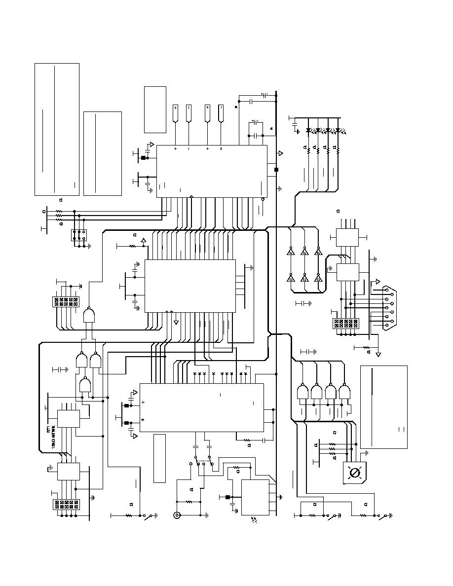
APPENDIX B Schematics
U4
M4-64/32
INTERF
A
CE
CPLD
37
36
35
34
33
32
31
30
25
24
23
22
21
20
19
18
15
14
13
IDPM1
IDPM0
ZL
L/RCLK
BCLK
SD
A
T
A
DEEMPH
ZR
MCLK
O
LZR
LZL
LDEEMPH
SLCT_B
M2
SLCT_C
SLCT_A
DEEMPH
I/O31
I/O30
I/O29
I/O28
I/O27
I/O26
I/O25
I/O24
I/O23
I/O22
I/O21
I/O20
I/O19
I/O18
I/O17
I/O16
I/O15
I/O14
I/O13
DV
D
D
D4
R35
10k
C11
100nF
38
16
C10
100nF
DV
D
D
V
CC
V
CC
GND
GND
17
6
40
4
7
26
29
5
27
41
42
43
44
1
2
3
8
9
10
11
12
TDI
TCK
TMS
TDO
CLK0/10
CLK1/11
I/O0
I/O1
I/O2
I/O3
I/O4
I/O5
I/O6
I/O7
I/O8
I/O9
I/O10
I/O11
I/O12
GND
GND
39
28
IMCLK
EMCLK
D3
EBCLK
ELRCLK
ESD
A
T
A
VERF
ISD
A
T
A
M1
M0
PREEMPH
ILRCLK
IBCLK
L
VERF
SPDIF/EXT
U11C
HC00
9
10
8
M
CLK
TDI
TCK
TMS
TDO
DV
D
D
J4
ISP POR
T
1
TCK
TMS
TDI
TDO
3
CLA
T
23
MUTE
9
DEEMPH
20
IDPM1
21
IDPM0
2
MCLK
26
BCLK
25
L/RCLK
27
SD
A
T
A
5
CD
A
T
A
4
CCLK
22
ZL
8
ZR
SD
A
T
A
L/RCLK
BCLK
MCLK
IDPM0
IDPM1
DEEMPH
MUTE
CLA
T
CH
CCLK
CD
A
T
A
ZER
OR
ZER
OL
24
RST
RESET
6
7
10
96/48
192/48
NC
U3
AD1852JRS
OUTL
OUTL
OUTR
OUTR
16
12
13
14
17
19
15
FIL
T
R
FIL
T
B
A
GND
C9
100nF
C5
100nF
C22
15 F
10V T
ANT
C23
15 F
10V T
ANT
A
GND
AGND
DGND
FB3
600Z
R
OUT
R
OUT
LOUT
LOUT
18
AV
D
D
C6
100nF
DV
D
D
C7
100nF
28
FB5
600Z
AV
D
D
DV
D
D
AD1852
STEREO D
A
C
JP1
SELECT
DV
D
D
R37
10k
10k
R5
R4
10k
S5
POSN
AD1852
I/F MODE
INTERF
A
CE
IDPM1
MODE
IDPM0
0
1
2
3
4
LJ
, 16-/20-/24-BIT
I2S, 16-/20-/24-BIT
RJ 24-BIT (DEF
A
U
L
T
)
DSP MODE
SPI CONTR
O
L
1
0
0
1
0
0
1
0
1
0
SAMPLE
RA
TE
INTERP
RA
TIO
INTERNAL
CLKRA
TE
MODE
96/48
192/48
MCLK
xFs
0
1
0
1
JP1 AD1852 MCLK/SR SELECT
0
0
1
1
32-48
96
192
8x
4x
2x
128Fs
64Fs
32Fs
PR
OHIBITED MODE
256,384,512,768,1024
128,192,256,384,512
64,96,128,192,256
R15
L
VERF
R14
LDEEMPH
R12
LZR
R13
LZL
392
392
392
392
DS4
DS3
DS2
DS1
DV
D
D
C8
100nF
VERF
DEEMPHASIS
ZER
O RIGHT
ZER
O LEFT
1
3
5
U5A
U5B
U5C
2
HC14
4
HC14
6
HC14
12 CLA
T
HC14
10 CCLK
HC14
8 CD
A
T
A
HC14
13
11
9
U5F
U5E
U5D
DV
D
D
R1
R2
R3
R4
C1
C2
C3
C4 GND GND
2
3
4
5
10
9
8
7
6
DV
D
D
6
10
9
8
7
2
3
4
5
R2
R4
R6
R8
R1
R3
R5
R7 GND GND
RT
2
10k NTWK
RC2
RCNTWK
MCLK
O
CLA
T
CCLK
CD
A
T
A
D0
D2
D1
1
DV
D
D
D4
5
9
4
8
3
7
2
6
1
J5
PCPOR
T
J3
SPI CONTR
O
L POR
T
DV
D
D
C41
100nF
D3
DV
D
D
R36
10k
DV
D
D
C42
100nF
DGND
U10A
HC00
U10B
HC00
U10C
HC00
U10D
HC00
1
2
3M
0
4
5
6M
1
9
10
8M
2
12
13
11
M3
M0
M1
M2
RST
DV
D
D
DV
D
D
10k
R9
10k
R11
10k
R10
SLCT_A
SLCT_B
SLCT_C
2
6
4
0
S5
INTERF
A
CE MODE
1
2
4
C
MUTE
DEEMPH
DV
D
D
S4
DEEMPH
10k
R8
10k
R6
S2
MUTE
S5
MODE
CS8414 OUTPUT
I/F MODE FORMA
T
0
1
2
3
4
5
6
LEFT JUST INV SCK, 16-/24-BIT
12S,
16-/24-BIT
,
1 LSB DELA
Y
RIGHT JUST
,
24-BIT
DSP WSYNC, 16-/24-BIT
SPI CONTR
O
LLED
19
IMCLK
12
IBCLK
11
ILRCLK
26
ISD
A
T
A
23
M0
24
M1
18
M2
17
M3
1
14
15
28
25
6
5
4
3
2
27
16
13
DV
D
D
SD
A
T
A
FSYNC
SCK
MCK
M0
M1
M2
M3
C
U
CBL
VERF
ERF
C0/E0
Ca/E1
Cb/E2
Cc/F0
Cd/F1
Ce/F2
SEL
CS12/FCK
U2
CS8414CS
DGND
A
GND
8
21
20
FIL
T
475
R3
C19
68nF
C2
10nF
C1
10nF
10
9
RXN
RXP
S1
75.0
R1
1
0
J1
SPDIF I/P
SIGNAL SOURCE
2
4
5
6
SHLD
SHLD
DGND
DGND
3
1
DVD
D
OUT
T
O
SLINK I/P
U1
T
ORX173
DV
D
D
C4
100nF
FB1
600Z
SPDIF
RCVR
VA
VD
C20
100nF
C21
100nF
FB2
600Z
22
7
T
O
PIN 21
T
O
PIN 8
DV
D
D
FB4
600Z
DV
D
D
S3
SPDIF/EXT
10k
R7
SPIDIF/EXT
U11D
HC00
12
13
11
U11B
HC00
4
5
6
U11A
HC00
1
2
3
6
10
9
8
7
2
3
4
5
R2
R4
R6
R8
R1
R3
R5
R7 GND GND
DV
D
D
R1
R2
R3
R4
C1
C2
C3
C4 GND GND
2
3
4
5
10
9
8
7
6
ESD
A
T
A
ELRCLK
EBCLK
EMCLK
DV
D
D
C43
100nF
1
DV
D
D
J2
RC1
RCNTWK
EXT DA
T A
INTERF A
CE
1
11
1
1
1
1
R2
3.40k
Figure 1. SPDIF Receiver, Interface CPLD and AD1852 DAC Circuits
REV. 0
EVAL-AD1852EB
9
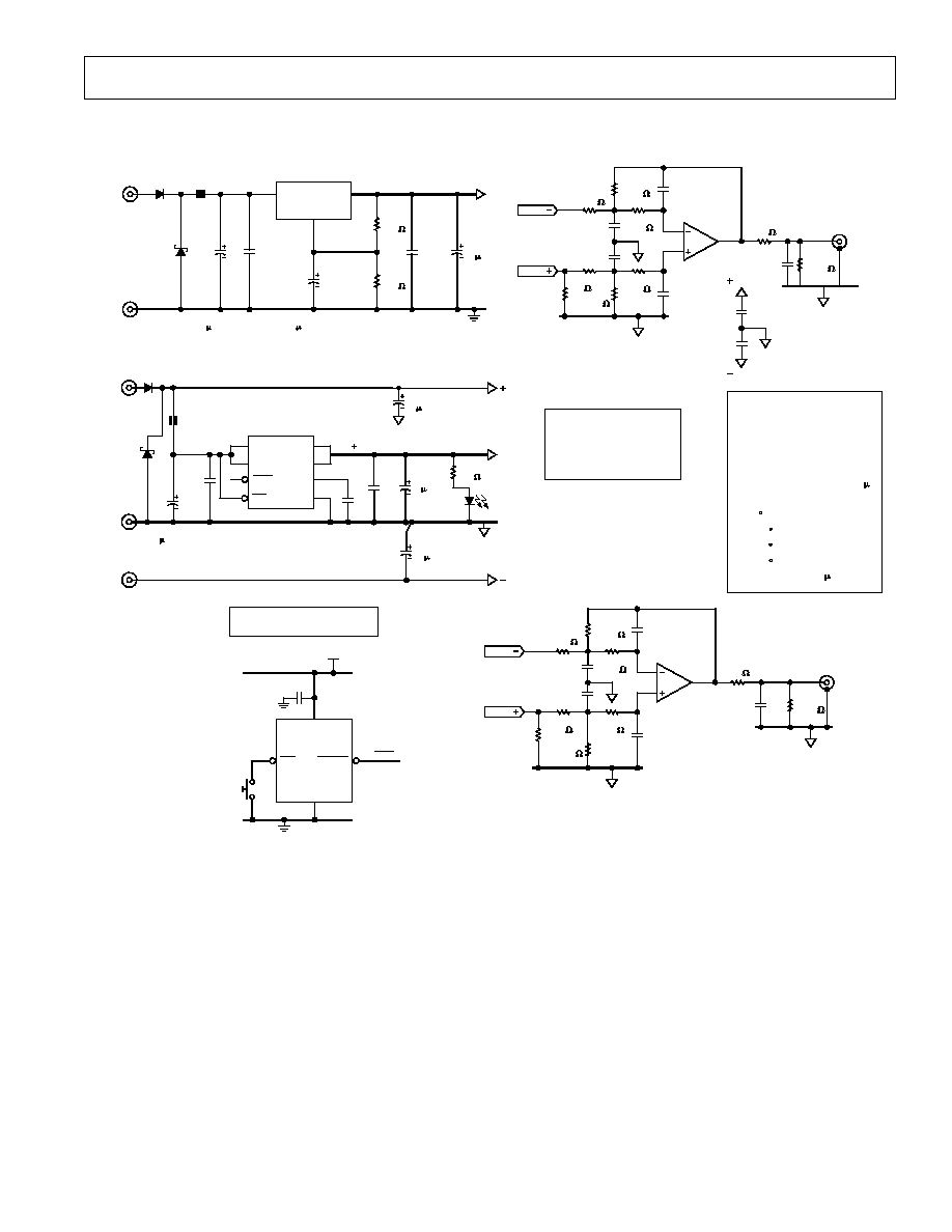
RESET GENERATOR
VCC
GND
MR
RESET
DVDD
C16
100nF
4
U8
ADM811TART
2 RST
3
1
DGND
RESET
S6
PLEASE NOTE: R38, R39
OPTIONAL RESISTORS.
TRIM TO REDUCE THD
WITH AD1855 UP TO 6dB
7
6
5
LOUT
AV
CC
C18
100nF
C17
100nF
AV
CC
R38
OPTION
C30
1.0nF NP0
C29
2.7nF PPS
R21
2.80k
C25
270pF NP0
C26
820pF NP0
AGND
R24
1.0k
U9B
OP275GP
C33
2.2nF PPS
J6
LEFT OUT
0
1
BESSEL LP FILTER RESPONSE
CORNER FREQUENCY: 100kHz
0.11dB @ 20kHz
0.45dB @ 40kHz
STEP RESPONSE:
<1% OVERSHOOT @ 7.75
LINEAR PHASE:
0 @ 20kHz
20 @ 20kHz
40 @ 40kHz
60 @ 60kHz
s
V
IN
V
OUT
GND
U6
LM317MDT
3
4
1
C12
100nF
10V TANT
15 F
C24
243
R33
715
R34
C13
100nF
16V A1
47 F
C36
5V REG
16V A1
47 F
C35
FB7
600Z
CR1
1SMB15AT3
DVDD
DGND
CR3
DL4001
J8
J9
IN
IN
ERR
SD
OUT
OUT
NR
GND
1
2
3
4
8
7
6
5
J11
C14
100nF
16V A1
47 F
C37
CR4
DL4001
J10
CR2
SMB15AT3
FB6
600Z
U7
ADP33035.0
C3
10nF
C15
100nF
16V A1
47 F
C38
5V REG
C39
392
R16
DS5
POWER
AVDD
AV
CC
C40
J12
AV
CC
AGND
R18
499
R29
549
R17
1.50k
R23
806
R22
3.01k
R31
53.6k
1
2
3
ROUT
ROUT
R39
OPTION
C32
1.0nF NP0
C31
2.7nF PPS
R25
2.80k
C27
270pF NP0
C28
820pF NP0
AGND
R28
1.0k
U9A
OP275GP
C34
2.2nF PPS
J7
RIGHT OUT
0
1
R20
499
R30
549
R19
1.50k
R27
806
R26
3.01k
R32
53.6k
AGND
12V
+12V
DGND
9-12
VOLTS
GROUP DELAY: 2.83 s
LOUT
16V A1
47 F
16V A1
47 F
Figure 2. Anti-Image Filters, Power Supply Regulation, Reset Generator
REV. 0
EVAL-AD1852EB
10
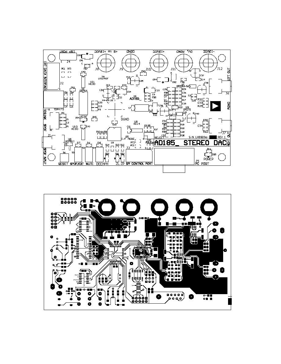
APPENDIX C Printed Circuit Board
Figure 3. Silk Screen
Figure 4. Top Layer (Component Side)
REV. 0
EVAL-AD1852EB
11
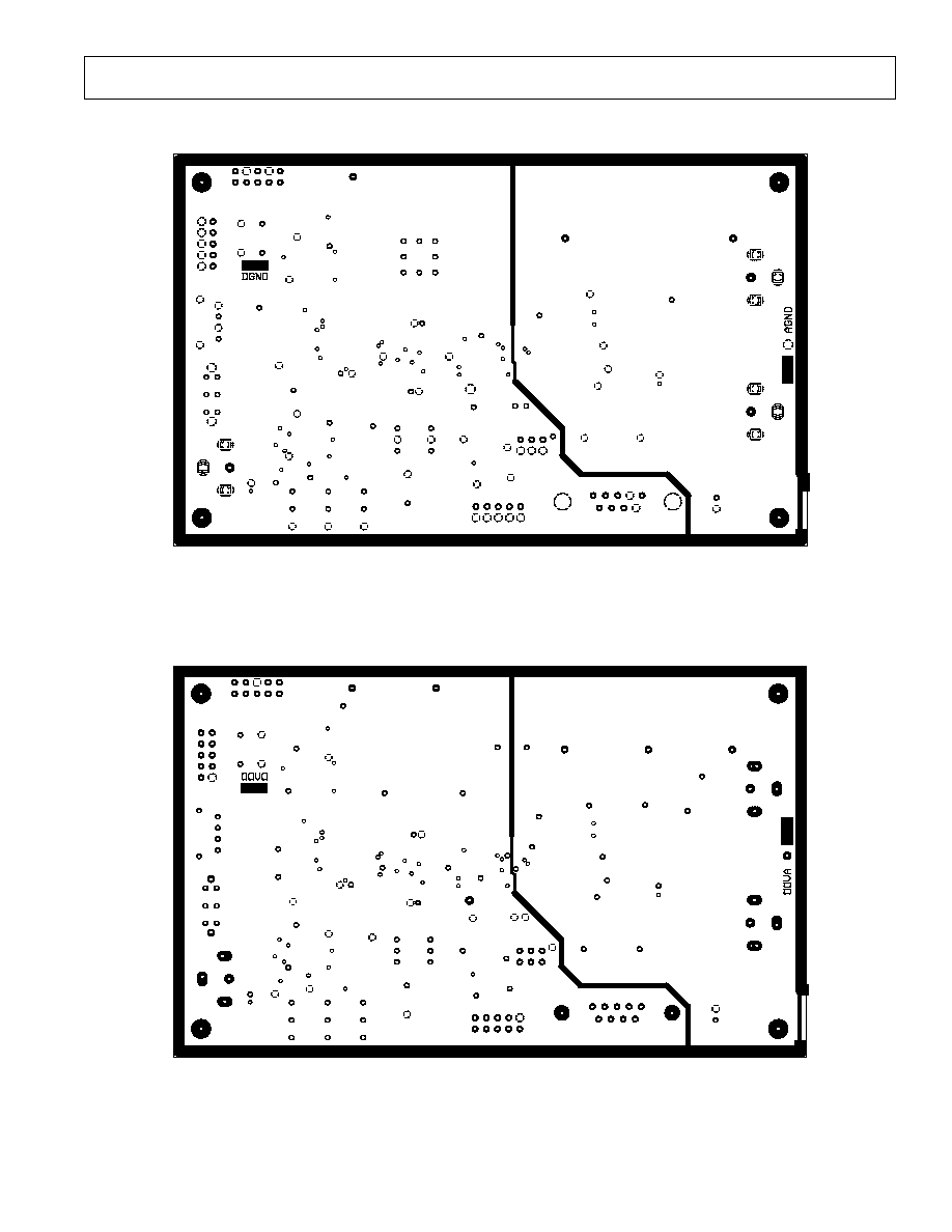
Figure 6. Power Planes
Figure 5. Ground Planes
REV. 0
EVAL-AD1852EB
12
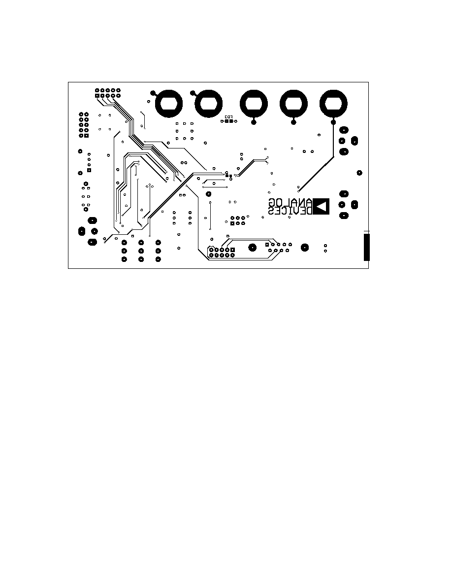
Figure 7. Bottom Layer (Solder Side)
REV. 0
EVAL-AD1852EB
13
APPENDIX D Parts List
Bill of Materials for AD1852EB
Qty.
Used
Part Type
Designator
Footprint
Description
3
10nF
C1, C2, C3
SMD 0805
10%, 50 V, X7R Multilayer Ceramic Capacitor
20
100nF
C4, C5, C6, C7, C8, C9,
SMD 0805
10%, 50 V, X7R Multilayer Ceramic Capacitor
C10, C11, C12, C13, C14,
C15, C16, C17, C18,
C20, C21, C41, C42, C43
1
68nF
C19
SMD 0805
10%, 50 V, X7R Multilayer Ceramic Capacitor
3
15uF 10V Tant
C22, C23, C24
EIA Size B
20%, 10 VW, Tantalum Electrolytic Capacitor
2
270pF NP0
C25, C27
SMD 0805
5%, 50 V, NP0 Multilayer Ceramic Chip Capacitor
2
820pF NP0
C26, C28
SMD 0805
5%, 50 V, NP0 Multilayer Ceramic Chip Capacitor
2
2.7nF PPS
C29, C31
SMD 1206
5%, 50 V, PPS Plastic Film Chip Capacitor
2
1.0nF NP0
C30, C32
SMD 0805
5%, 50 V, NP0 Multilayer Ceramic Chip Capacitor
2
2.2nF PPS
C33, C34
SMD 0805
5%, 50 V, PPS Plastic Film Chip Capacitor
6
47
µF 16V Al
C35, C36, C37, C38,
Size Code D
20%, 16 VW, Low Impedance Aluminum Electrolytic
C39, C40
2
1SMB15AT3
CR1, CR2
SMD 403A
600 W, Transient Voltage Supppressor Zener Diode
2
DL4001
CR3, CR4
SOD80
50 V, 1A Diode/Rectifier
1
ZERO LEFT
DS1
SMD 1206
Red, Light Emitting Diode
1
ZERO RIGHT
DS2
SMD 1206
Red, Light Emitting Diode
1
DEEMPHASIS
DS3
SMD 1206
Red, Light Emitting Diode
1
VERF
DS4
SMD 1206
Red, Light Emitting Diode
1
POWER
DS5
SMD 1206
Red, Light Emitting Diode
7
600Z
FB1, FB2, FB3, FB4,
SMD 0805
600
@ 100 MHz, <1.0 DC, 200 mA Ferrite Bead
FB5, FB6, FB7
1
75.0
R1
SMD 0805
1%, 100 mW, Thick Film SMD Resistor
1
3.40k
R2
SMD 0805
1%, 100 mW, Thick Film SMD Resistor
1
475
R3
SMD 0805
1%, 100 mW, Thick Film SMD Resistor
11
10k
R4, R5, R6, R7, R8, R9,
SMD 0805
1%, 100 mW, Thick Film SMD Resistor
R10, R11, R35, R36, R37
5
392
R12, R13, R14, R15, R16
SMD 0805
1%, 100 mW, Thick Film SMD Resistor
2
1.50k
R17, R19
SMD 0805
1%, 100 mW, Thick Film SMD Resistor
2
499
R18, R20
SMD 0805
1%, 100 mW, Thick Film SMD Resistor
2
2.80k
R21, R25
SMD 0805
1%, 100 mW, Thick Film SMD Resistor
2
3.01k
R22, R26
SMD 0805
1%, 100 mW, Thick Film SMD Resistor
2
806
R23, R27
SMD 0805
1%, 100 mW, Thick Film SMD Resistor
2
1.0k
R24, R28
SMD 0805
1%, 100 mW, Thick Film SMD Resistor
2
549
R29, R30
SMD 0805
1%, 100 mW, Thick Film SMD Resistor
2
53.6
R31, R32
SMD 0805
1%, 100 mW, Thick Film SMD Resistor
1
243
R33
SMD 0805
1%, 100 mW, Thick Film SMD Resistor
1
715
R34
SMD 0805
1%, 100 mW, Thick Film SMD Resistor
2
option
R38, R39
SMD 0805
1%, 100 mW, Thick Film SMD Resistor
2
RC NTWK
RC1, RC2
SMD EZAST32
Panasonic 100
/47pF Chip RC Network
2
10k
NTWK
RT1, RT2
SMD EXBE 10
Panasonic 10 k
Chip Resistor Network
1
SPDIF INPUT
J1
PCB Thru Hole
Right Angle PCB Mount RCA Jack
1
EXT DATA INTERFACE
J2
2
×5, 0.1" PCB Thru Hole 10-Pin Vertical Shrouded Header
1
SPI CONTROL PORT
J3
2
×5, 0.1" PCB Thru Hole 10-Pin Vertical Shrouded Header
1
ISP PORT
J4
2
×5, 0.1" PCB Thru Hole 10-Pin Vertical Shrouded Header
1
PC PORT
J5
DB9 PCB Thru Hole
Right Angle, 9-Pin Male D-Sub Connector
1
LEFT OUT
J6
PCB Thru Hole
Right Angle PCB Mount RCA Jack
1
RIGHT OUT
J7
PCB Thru Hole
Right Angle PCB Mount RCA Jack
1
+9 to +12VDC
J8
PCB Thru Hole
RED, Screw Terminal/Banana Post
1
DGND
J9
PCB Thru Hole
BLK, Screw Terminal/Banana Post
1
+12VDC
J10
PCB Thru Hole
ORG, Screw Terminal/Banana Post
1
AGND
J11
PCB Thru Hole
GRN, Screw Terminal/Banana Post
1
12VDC
J12
PCB Thru Hole
BLU, Screw Terminal/Banana Post
1
SELECT
JP1
3
×2, 0.1", PCB Thru Hole 6-Pin Vertical Header

REV. 0
EVAL-AD1852EB
14
Qty.
Used
Part Type
Designator
Footprint
Description
31
SPDIF/TOSLINK
S1
PCB Thru Hole
Right Angle Mount DPDT Slide Switch
1
MUTE
S2
2
×5, 0.1" PCB Thru Hole 10-Pin Vertical Shrouded Header
1
SPDIF/EXT
S3
PCB Thru Hole
Vertical Slide SPST Switch
1
DEEMPH
S4
PCB Thru Hole
Vertical Slide SPST Switch
1
INTERFACE MODE
S5
PCB Thru Hole
8-Position, OCTAL Code, PCB Binary Switch
1
RESET
S6
SMD
Normally Open Push Button Switch
1
TORX173
U1
PCB Thru Hole
TOSLink Digital Audio Fibre Optic Receiver
1
CS8414-CS
U2
SOIC-28L
AES/EBU Digital Audio Interface Receiver
1
AD1852JRS
U3
28-LEAD SSOP
High Performance 24-BIT, 192kHz, Stereo DAC
1
M4-64/32-15VC
U4
TQFP-44
Vantis, MACH-4 Series ISP CPLD
1
74HC14M
U5
SO-14
Schmitt Trigger Hex Inverter
1
LM317MDT
U6
DPAK
Adjustable, 3-Term Voltage Regulator
1
ADP3303AR-5
U7
SO-8
Low Noise, Low Drop Out, Five Volt Regulator
1
ADM811TART
U8
SOT-143
200ms, Power-Up/Manual Reset Generator
1
OP275GS
U9
SO-8
High Performance Audio Op Amp
2
74HC00M
U10, U11
SO-14
Quad 2-Input Nand Gate
C007382.51/01 (rev. 0)
PRINTED IN U.S.A.
Document Outline
- Specifications
- Ordering Guide
- Functional Block Diagram
- Schematic
- OVERVIEW
- AD1852 OVERVIEW
- FUNCTIONAL DESCRIPTION
- POWER SUPPLIES
- EXTERNAL SPI CONTROL PORT
- AUDIO SIGNAL OUTPUTS
- INTEGRATED CIRCUIT FUNCTIONS
- PERFORMANCE SPECIFICATIONS
- ATTACHMENTS
- FURTHER INFORMATION
- DIAGRAMS
- SPDIF Receiver, Interface CPLD and AD1852 DAC Circuits
- Anti-Image Filters, Power Supply Regulation, Reset Generator
- Silk Screen
- Top Layer (Component Side)
- Ground Planes
- Power Planes
- Bottom Layer (Solder Side)