Äîêóìåíòàöèÿ è îïèñàíèÿ www.docs.chipfind.ru

One Technology Way, P.O. Box 9106, Norwood. MA 02062-9106, U.S.A.
Tel: 617/329-4700
Fax: 617/326-8703
REV. A
Information furnished by Analog Devices is believed to be accurate and
reliable. However, no responsibility is assumed by Analog Devices for its
use, nor for any infringements of patents or other rights of third parties
which may result from its use. No license is granted by implication or
otherwise under any patent or patent rights of Analog Devices.
a
Evaluation Board for 10-bit high speed,
low power, successive-approximation ADC
EVAL-AD7470CB
FUNCTIONAL BLOCK DIAGRAM
FEATURES
Full-Featured Evaluation Board for the AD7470
EVAL-CONTROL BOARD Compatible
HSC-INTERFACE BOARD Compatible
Stand Alone Capability
On-Board Analog Buffering and Reference
Optional On-Board Analog Bias-Up Circuit
Optional On-Board Burst Clock Generator Circuit
Various Linking Options
PC Software for Control and Data Analysis when used
with EVAL-CONTROL BOARD
I N T R O D U C T I O N
This Technical Note describes the evaluation board for the
AD7470 10-bit, high speed, low power, successive approxi-
mation A/D converter that operates from a single 2.7 V to
5.25 V supply. Full data on the AD7470 is available in the
AD7470 data sheet available from Analog Devices and
should be consulted in conjunction with this Technical Note
when using the Evaluation Board.
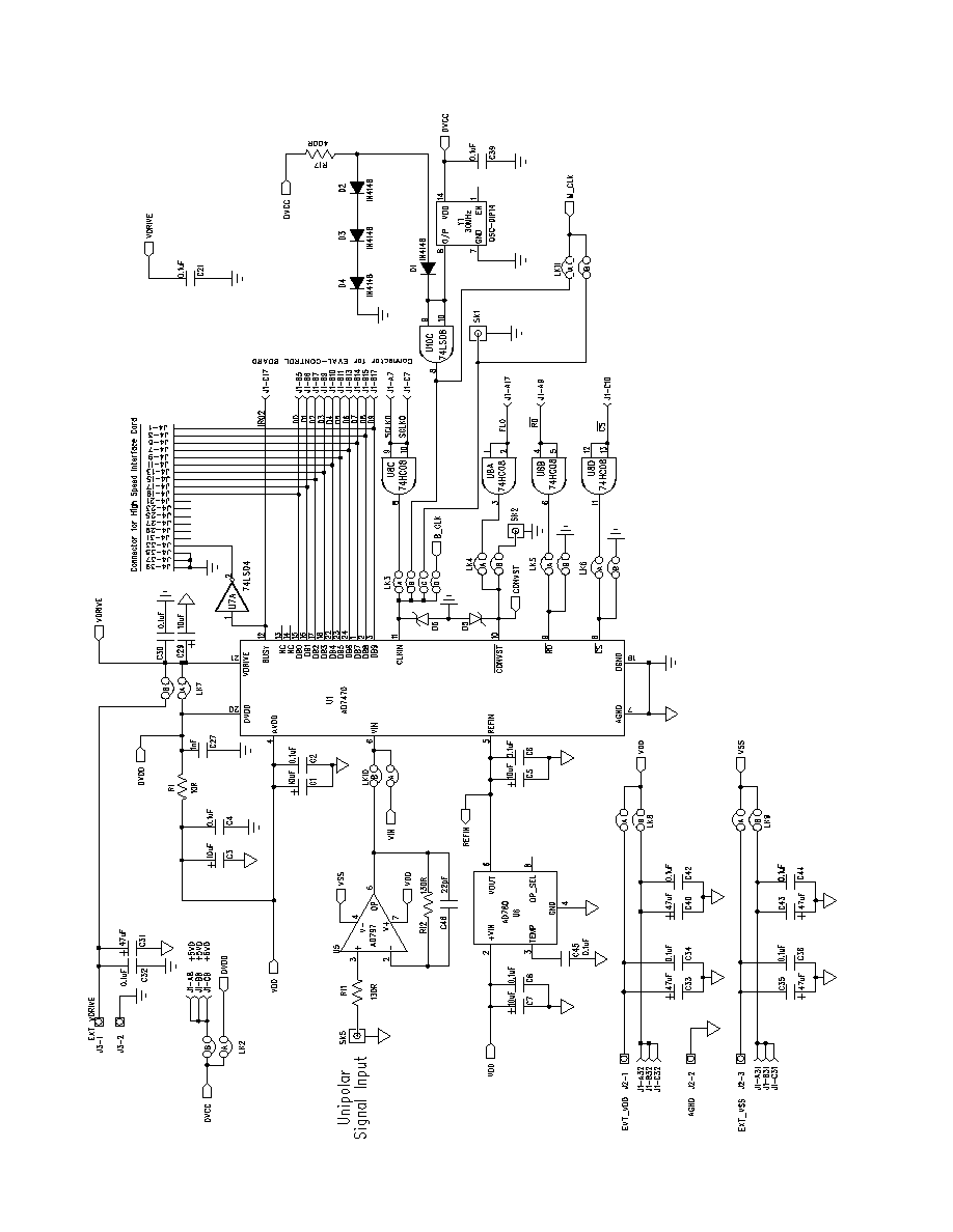
On-board components include an AD780 which is a pin
programmable +2.5 V or +3 V ultra high precision bandgap
reference, two AD797 op-amps used to buffer the analog
input, and an OP07 op-amp used to buffer the DC bias
voltage applied to the optional analog input bias-up circuit.
There are various link options which are explained in detail
on page 2.
Interfacing to this board is through a 96-way connector. This
96-way connector is compatible with the EVAL-CONTROL
BOARD which is also available from Analog Devices.
External sockets are provided for the
CONVST input,
CLKIN input and the VIN inputs.
OPERATING THE AD7470 EVALUATION BOARD
Power Supplies
When using this evaluation board with the EVAL-CON-
TROL BOARD all supplies are provided from the EVAL-
CONTROL BOARD through the 96 way connector.
When using the board as a stand alone unit or with the HSC-
INTERFACE BOARD, external supplies must be provided.
This evaluation board has five power supply inputs: V
DD
,
A
GND
, V
SS
, V
DRIVE
and D
GND
. +5 V must be connected to the
V
DD
input to supply the AV
DD
and DV
DD
pins on the AD7470,
the AD780 voltage reference, the positive supply pin of all
three op-amps and the digital control logic. 0 V is connected
to the A
GND
input. -5 V must be connected to the V
SS
input to
supply the negative supply pins on all three op-amps. The
V
DRIVE
input can be used to provide an external voltage for the
output drivers on the AD7470. If an external V
DRIVE
is
supplied, it is referenced to the D
GND
input which should be
tied to 0 V. The supplies are decoupled to the relevant ground
plane with 47µF tantalum and 0.1µF multilayer ceramic
capacitors at the point where they enter the board. The supply
pins of the op-amps and reference are also decoupled to A
GND
with a 10µF tantalum and a 0.1µF ceramic capacitor. The
AD7470 AV
DD
supply pin is decoupled to A
GND
with 10uF
tantalum and 0.1µF multilayer ceramic capacitors. The
AD7470 DV
DD
and VDRIVE pins are decoupled to A
GND
with
10uF tantalum capacitors and to D
GND
with 0.1µF multilayer
ceramic capacitors.
Extensive ground planes are used on this board to minimize
the effect of high frequency noise interference. There are two
ground planes, A
GND
and D
GND
. These are connected at one
location close to the AD7470.
V in
U nipolar
A in
B ipolar
A in
R efin
R e fe ren ce
B uffe r
B ia s-u p
buff er
C lo ck
G e ne rator
C irc uits
40 pin H S C in ter fa ce
96 P
i
n E
v
al
-
C
ont
r
o
l
Bo
a
rd
I
nt
er
fa
ce
D a ta B u s
C o ntro l Line s
A D 7470 A D C
P ow er S upply C ircuit
Note: For Eval-AD7470CB Rev. B, the maxi-
mum throughput rate is 1.5 MHz.

EVAL-AD7470CB
2
REV. 0
Analog Input Section
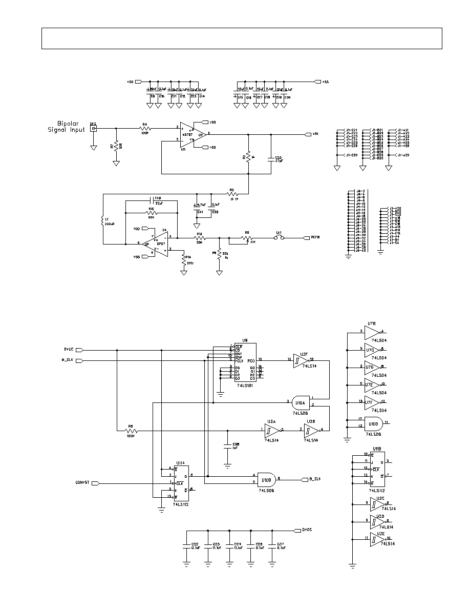
The analog input section of this evaluation board accommodates unipolar and bipolar signals. Unipolar signals within the
AD7470 analog input signal range of 0 V - 2.5 V are connected via SK5. They are then buffered by the on-board buffer before
being applied to the VIN pin of the AD7470. Bipolar signals are connected via SK3 and are biased up by the on-board bias-
up buffer circuit before being applied to the VIN pin of the AD7470. The input impedence of the bias-up circuit is 50
which
is determined by the value of R7. The input impedence may be modified by removing/changing the value of R7. To obtain
optimum performance from this evaluation board the use of an impedence matched, passive filter is recommended before the
analog signal is applied to the evaluation board. For example, when using a 100KHz input tone, a 100KHz 50
filter from
TTE (part number KC5-100K-15K-50/50-720B) is suitable.
R8 Potentiometer (50Kohm)
This variable resistor is used to trim the DC bias voltage applied to the optional analog input bias-up circuit. This bias voltage
is factory preset to 1.25 V which biases a bipolar signal to swing around the midpoint of the analog input range (0 - 2.5 V).
If any adjustment is required, the user can use the histogram window in the eval-board software to analyze the DC voltage
variation while adjusting the trim pot. To view this properly, an analog input signal should not be applied to the board. Under
normal operation this pot should not be adjusted as it is preset for optimum performance.
LINK AND SWITCH OPTIONS
There are 11 link options which must be set for the required operating setup before using the evaluation board. The functions
of these options are outlined below.
Link No.
Function.
LK1
This link is used to select the DC bias voltage to be applied to the optional Vin bias-up circuit.
If the user is using the bias-up circuit, this link must be inserted which will apply the 2.7 V reference voltage
to the bias-up circuit. This causes a bipolar signal (applied to the bipolar vin input socket) to be biased up
around +1.25 V before it is applied to the AD7470 VIN pin. - see also LK10 (below)
If the bias up circuit is not being used this link should be removed.
LK2
This link must be in position "A" if external power supplies are being used. In this position the control logic
is being powered by the voltage applied to the VDD input.
When power is being supplied from the EVAL-CONTROL BOARD, this link can be moved to position "B"
if the user wants to drive the control logic from a separate +5 V which is generated on the EVAL-CONTROL
B O A R D .
LK3
This link option selects the source of the CLKIN input.
When this link is in position "A" the CLKIN input is provided by the EVAL-CONTROL BOARD.
When this link is in position "B" the CLKIN input is provided via the on-board 25MHz oscillator.
When this link is in position "C", an external CLKIN signal must be provided via SK1.
When using the on-board generated burst clock, this link must be in position "D".
LK4
This link option selects the source of the
CONVST input.
When this link is in position "A" the
CONVST input is provided by the EVAL-CONTROL BOARD.
When this link is in position "B" the
CONVST input is provided via the external socket, SK2.
LK5
This link option selects the source of the
RD input.
When this link is in position "A" the
RD input is provided by the EVAL-CONTROL BOARD.
When this link is in position "B" the
RD input is tied to GND. This option must be selected while using the
High Speed Converter Interface Board.
LK6
This link option selects the source of the
CS input.
When this link is in position "A" the
CS input is provided by the EVAL-CONTROL BOARD.
When this link is in position "B" the
CS input is tied to GND. This option must be selected while using the
High Speed Converter Interface Board.
LK7
This link option sets the voltage applied to the VDRIVE pin on the AD7470.
When this link is in position "A", VDRIVE is connected directly to the DVDD pin.
When this link is in position "B", an external voltage must be applied to the VDRIVE pin Via J3.
LK8
This link selects the source of the V
DD
supply.
When this link is in position "A" V
DD
must be supplied from an external source via J2.
When this link is in position "B" V
DD
is supplied from the EVAL-CONTROL BOARD.
LK9
This link selects the source of the V
SS
supply.
When this link is in position "A" V
SS
must be supplied from an external source via J2.
When this link is in position "B" V
SS
is supplied from the EVAL-CONTROL BOARD.
LK10
This link must be in position "A" if a bipolar AIN signal is being applied to the bipolar Vin socket, SK3.
This link must be in position "B" if a unipolar AIN signal is being applied to the unipolar Vin socket, SK5.

EVAL-AD7470CB
REV. 0
3
LK11
This link is used to provide a clock signal path to the burst mode circuit generator from either the on-board
clock oscillator or from an extermnal clock source via SK1.
In position "A" the master clock signal is provided from the on-board crystal oscillator.
In position "B" the master clock signal must be provided from an external source via SK1.
SET-UP CONDITIONS
Care should be taken before applying power and signals to the evaluation board to ensure that all link positions are as per the
required operating mode. Table I shows the position in which all the links are set when the evaluation board is sent out. All
links are set for use with the EVAL-CONTROL BOARD.
Table I. Initial Link and Switch Positions
Link No.
Position
Function.
LK1
Inserted
Provides DC bias voltage to the analog bias-up circuit.
LK2
A
The digital logic circuitry is powered from the same voltage as the AD7470.
LK3
A
CLKIN signal is provided by the EVAL-CONTROL BOARD via J1.
LK4
A
CONVST signal is provided by the EVAL-CONTROL BOARD via J1.
LK5
A
RD signal is provided by the EVAL-CONTROL BOARD via J1.
LK6
A
CS signal is provided by the EVAL-CONTROL BOARD via J1.
LK7
A
AD7470 VDRIVE pin is connected to the AD7470 DVDD pin.
LK8
B
V
DD
is supplied by the EVAL-CONTROL BOARD via J1.
LK9
B
V
SS
is supplied by the EVAL-CONTROL BOARD via J1.
LK10
A
The AD7470 Vin pin is connected to the output of the bias-up circuit.
LK11
A
Master clock for burst clock generator is provided from the on-board clock oscillator.
EVAL-AD7470CB
4
REV. 0
EVAL-CONTROL BOARD INTERFACING
Interfacing to the EVAL-CONTROL BOARD is via a 96-
way connector, J1. The pinout for the J1 connector is shown
in Figure 2 and its pin designations are given in Table II.
1
32
1
32
A
B
C
Figure 2. Pin Configuration for the 96-Way
Connector, J1
96-Way Connector Pin Description
D0-D11
Data Bit 0 to Data Bit 11. Three-state TTL
outputs. D11 is the MSB.
SCLK0
Serial Clock Zero. This continuous clock can be
connected to the CLKIN pin of the AD7470 via
LK3.
+5VD
Digital +5 V supply. This can be used to provide
a separate +5 V supply for the digital logic if
required via LK2.
R D
Read. This is an active low logic input connected
to the
RD pin of the AD7470 via LK5.
C S
Chip Select. This is an active low logic input
connected to the
CS pin of the AD7470 via LK6.
F L 0
Flag zero. This logic input is connected to the
CONVST input of the AD7470 via LK4.
IRQ2
Interrupt Request 2. This is a logic output and is
connected to the BUSY logic output on the
AD7470.
D G N D
Digital Ground. These lines are connected to
the digital ground plane on the evaluation
board. It allows the user to provide the digital
supply via the connector along with the other
digital signals.
A G N D
Analog Ground. These lines are connected to
the analog ground plane on the evaluation
board.
AV
SS
Negative Supply Voltage. This provides a nega-
tive supply to the on-board op-amps via LK9.
AV
DD
Positive Supply Voltage. This provides a positive
supply to the op-amps, the reference, the AD7470
and the digital logic.
When interfacing directly to the EVAL-CONTROL BOARD,
all power supplies and control signals are generated by the
EVAL-CONTROL BOARD. However, due to the nature of
the DSP interface on the EVAL-CONTROL BOARD,
AD7470 sampling rates greater than 400 KHz are not
supported when interfacing the EVAL-AD7470CB directly
to the EVAL-CONTROL BOARD. To achieve sample rates
greater than 400 KHz, the HSC-INTERFACE BOARD
must be used. The HSC-INTERFACE BOARD is a board
designed to interface between evaluation boards for high
speed analog-to-digital converters and the EVAL-CON-
TROL BOARD. It can be ordered from Analog Devices
through the normal channels using the part number "HSC-
INTERFACE BOARD".
Table II. 96-Way Connector Pin Functions.
ROW A
ROWB
ROWC
1
2
D 0
3
D 1
4
D G N D
D G N D
D G N D
5
D 2
6
D 3
7
SCLK0
D 4
SCLK0
8
+5VD
+5VD
+5VD
9
R D
D 5
10
D 6
C S
11
D 7
12
D G N D
D G N D
D G N D
13
D 8
14
D 9
15
D10
16
D G N D
D G N D
D G N D
17
F L 0
D11
IRQ2
18
19
20
D G N D
D G N D
D G N D
21
A G N D
A G N D
A G N D
22
A G N D
A G N D
A G N D
23
A G N D
A G N D
A G N D
24
A G N D
A G N D
A G N D
25
A G N D
A G N D
A G N D
26
A G N D
A G N D
A G N D
27
A G N D
28
A G N D
29
A G N D
A G N D
A G N D
30
A G N D
31
AVSS
AVSS
AVSS
32
AVDD
AVDD
AVDD
Note : The unused pins of the 96-way connector are not shown.
EVAL-AD7470CB
REV. 0
5
HIGH SPEED CONVERTER (HSC) BOARD
INTERFACING
Interfacing to the HSC BOARD is via a 40-way connector,
J4. The pinout for the J4 connector is shown in Figure 3 and
its pin designations are given in Table III.
1
2
39
40
Figure 3. Pin Configuration for the 40-pin HSC
Interface Connector, J1
Table III. HSC Interface Connector Pin Functions.
Pin No.
Function
Pin No.
Function
1
D11
2
G N D
3
D10
4
G N D
5
D 9
6
G N D
7
D 8
8
G N D
9
D 7
10
G N D
11
D 6
12
G N D
13
D 5
14
G N D
15
D 4
16
G N D
17
D 3
18
G N D
19
D 2
20
G N D
21
D 1
22
G N D
23
D 0
24
G N D
25
N / C
26
G N D
27
N / C
28
G N D
29
N / C
30
G N D
31
N / C
32
G N D
33
BUSY
34
G N D
35
N / C
36
G N D
37
N / C
38
G N D
39
N / C
40
G N D
N/C = Not Connected.
40-Way Connector Pin Description
D0-D11
Data Bit 0 to Data Bit 11. Three-state TTL
outputs. D11 is the MSB.
BUSY
BUSY. This is a logic output and is connected to
the BUSY logic output on the AD7470 via an
inverting buffer.
G N D
Ground. These lines are connected to
the digital ground plane on the evaluation
board.
When interfacing to the High Speed Converter Interface
board, all required power supplies must be supplied from
external sources via the power terminal, J2.
The CLKIN signal can be generated on-board (using the
crystal oscillator or the burst clock generator circuit) or
provided externally via SK1.
The RD and CS inputs to the AD7470 must all be tied low
using LK5 and LK6 respectively.
The CONVST signal must be provided externally via SK1.
Due to the 25 MHz on-board crystal (not the maximum of
26 MHz as specified in the datasheet) the throughput rate will
not meet the maximum datasheet specification of 1.5 MSPS.
Refer to the documentation included with the HSC-INTER-
FACE BOARD for more information. Note, the HSC-
INTERFACE BOARD was designed for other high speed
ADC devices but it is compatible with the AD7470 evalua-
tion system.

EVAL-AD7470CB
6
REV. 0
S O C K E T S
There are four input sockets relevant to the operation of the
AD7470 on this evaluation board. The function of these
sockets is outlined in Table IV.
Table IV. Socket Functions
Socket
Function
SK1
Sub-Miniature BNC Socket for external clock
input.
SK2
Sub-Miniature BNC Socket for external
CONVST input.
SK3
Sub-Miniature BNC Socket for Bipolar ana-
log input The AD7470 can only accept analog
inputs in the range 0 V to REFIN. Bipolar
analog inputs in the range -1.25 V to +1.25 V
applied to this socket are biased up to the
acceptable AD7470 input range by the on-
board bias-up circuit before being applied to
the AD7470 VIN pin.
SK5
Sub-Miniature BNC Socket for unipolar ana-
log input. Analog inputs in the acceptable
AD7470 analog input range (0 V to REFIN)
are applied to this socket. The signal is then
buffered before it is applied to the AD7470
VIN pin.
C O N N E C T O R S
There are four connectors on the AD7470 evaluation board
as outlined in Table V.
Table V. Connector Functions
Connector
Function
J 1
96-Way Connector for EVAL-CONTROL
BOARD interface connections.
J 2
External VDD, VSS & AGND power connec-
tor.
J 3
External VDRIVE & DGND power connec-
tor.
J 4
40-Way Connector for HIGH SPEED CON-
VERTER INTERFACE BOARD connec-
tions.
OPERATING WITH THE EVAL-CONTROL BOARD
The evaluation board can be operated in a stand-alone mode
or operated in conjunction with the EVAL-CONTROL
BOARD (with or without the HSC-INTERFACE BOARD).
This EVAL-CONTROL BOARD is available from Analog
Devices under the order entry "EVAL-CONTROL BOARD".
When interfacing directly to this control board, all supplies
and control signals to operate the AD7470 are provided by
the EVAL-CONTROL BOARD when it is run under control
of the AD7470 software which is provided with the AD7470
evaluation board package. This EVAL-CONTROL BOARD
will also operate with all Analog Devices evaluation boards
which end with the letters CB in their title.
The 96-way connector on the EVAL-AD7470CB plugs
directly into the 96-way connector on the EVAL-CON-
TROL BOARD. No power supplies are required in the
system. The EVAL-CONTROL BOARD generates all the
required supplies for itself and the EVAL-AD7470CB. The
EVAL-CONTROL BOARD is powered from a 12 V AC
transformer. This is a standard 12 V AC transformer capable
of supplying 1 A current and is available as an accessory from
Analog Devices under the following part numbers:
EVAL-110VAC-US:
For use in the U.S. or Japan
EVAL-220VAC-UK:
For use in the U.K.
EVAL-220VAC-EU:
For use in Europe
These transformers are also available for other suppliers
including Digikey (U.S.) and Campbell Collins (U.K.).
Connection between the EVAL-CONTROL BOARD and
the serial port of a PC is via a standard RS-232 cable which
is provided as part the EVAL-CONTROL BOARD pack-
age. Please refer to the manual which accompanies the
EVAL-CONTROL BOARD for more details on the EVAL-
CONTROL BOARD package.
EVAL-AD7470CB
REV. 0
7
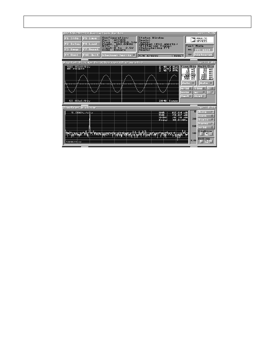
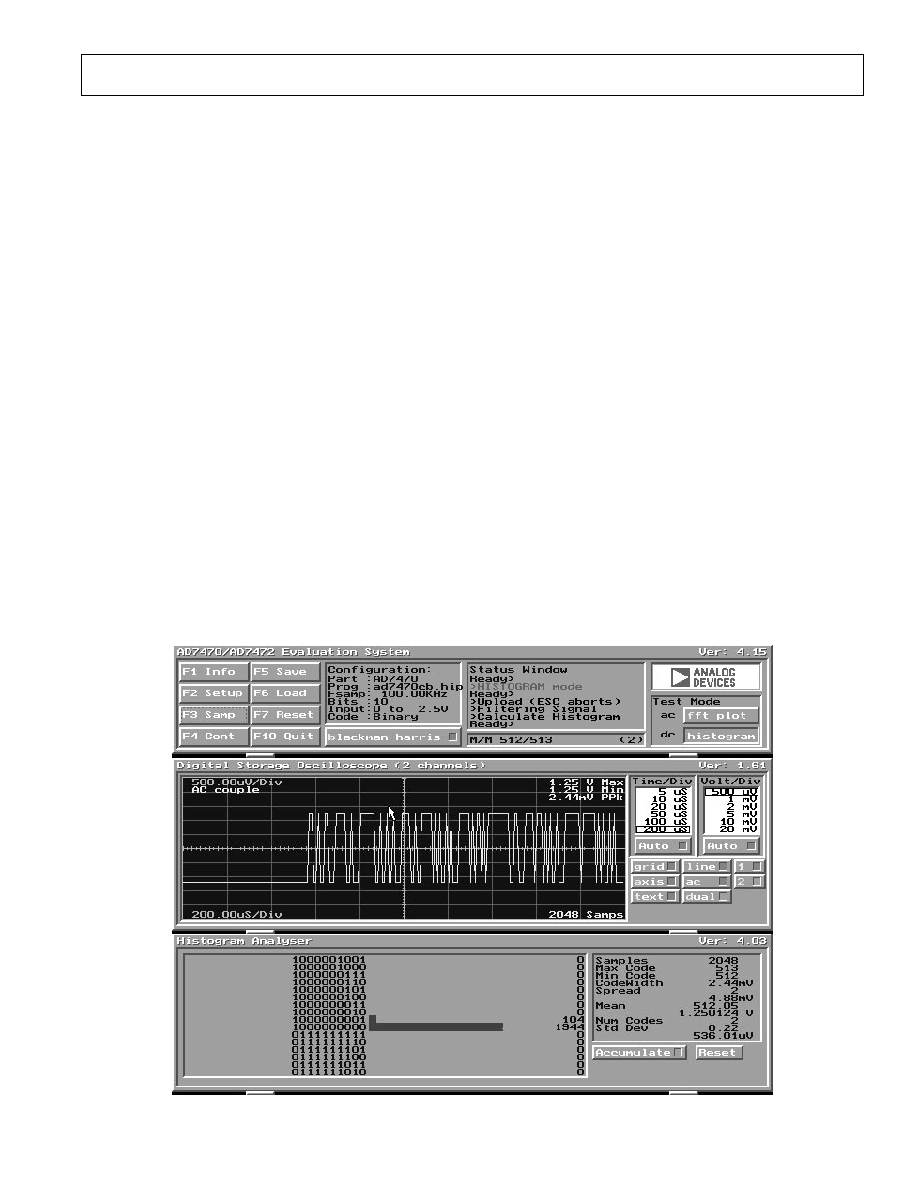
Figure 4. Main Screen
SOFTWARE DESCRIPTION
Included in the EVAL-AD7470CB evaluation board pack-
age is a PC-compatible disk. This disk has two sub-directo-
ries called EVAL_CTRL and HSC_INT, each containing
software for controlling and evaluating the performance of
the AD7470 when it is operated with the EVAL-CONTROL
BOARD or the HSC-INTERFACE BOARD. The EVAL-
AD7470CB Demonstration/Evaluation Software runs under
DOS 4.0 or later and requires a minimum of a 386-based
machine with 400kB of base RAM and 500kB of free hard
disk space. The user interface on the PC is a dedicated
program written especially for the AD7470.
The disk which accompanies the EVAL-AD7470CB con-
tains two sub-directories. The user should create a new
directory on the main PC drive and label this "AD7470".
Then, the sub-directories (and all files contained within
them) on the EVAL-AD7470CB disk should be copied into
this directory. The Mouse Driver on the PC should be
enabled before running the software. If this has not been
loaded, the program will not run.
To run the software, simply make the AD7470\EVAL_CTL
directory or the AD7470\HSC_INT directory (depending
on which setup is being used) the current directory and type
"go". When the evaluation program starts, the user sees the
screen shown on Figure 3 (without any FFT or scope
waveforms). This is the main screen and it is divided into
three parts. The top part provides the main control interface
for the AD7470 evaluation software. The middle part of the
main screen functions as a Digital Storage Oscilloscope and
the bottom part of the main screen operates as either a Digital
Spectrum Analyzer or a Histogram analyzer.
Each part of the screen has several buttons that can be pressed
by using the mouse or the keyboard. To press a button using
the mouse, simply use it to move the on-screen pointer to the
button to be activated and click. To use the keyboard, simply
press the appropriate key as highlighted on the button. Lower
case letters must be used. When a button is pressed, it is
highlighted on the screen. The next button can be high-
lighted by using the Tab key or the previous button by
holding down the shift key and the Tab key together. The
highlighted button can also be pressed by pressing the space
bar. Pressing the ESC key halts any operation currently in
progress. In this document, if a button can be activated from
the keyboard then the key used is shown in bold in the button
name. For example, "no prog" has the "p" highlighted in
bold, indicating that the button can be activated by pressing
the p key.
Some buttons have a red indicator. A red indicator on the
button means that the function associated with that button is
on. Absence of the red indicator light means that the function
associated with the button is off. The on/off status of these
buttons is changed simply by selecting the button.
Setting up the EVAL-CONTROL BOARD
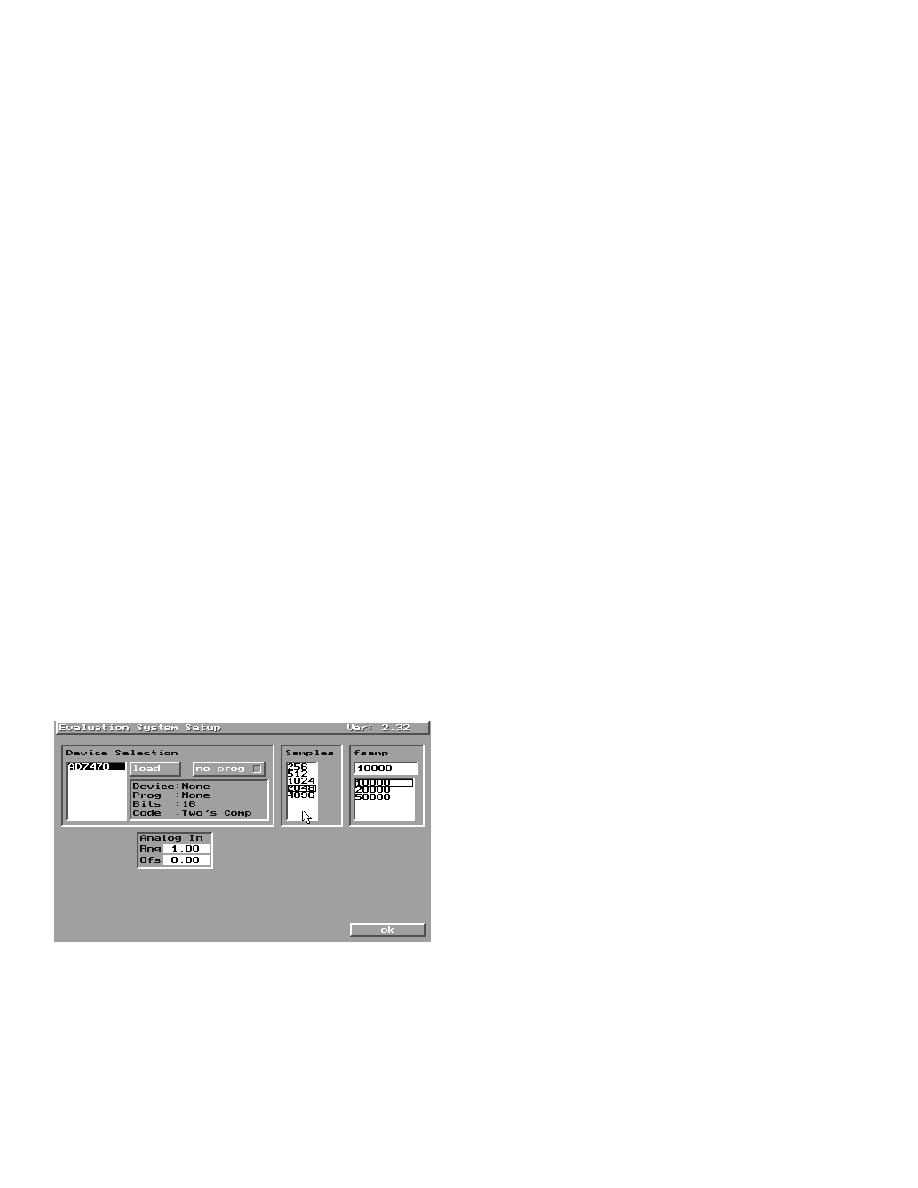
When the software is run, the "F2 Setup" button in the top left
of the screen should be selected to pop up the setup menu (see
fig. 4). This menu sets up the EVAL-CONTROL BOARD
for use with the EVAL-AD7470CB.
Firstly, a configuration file must be chosen. The configura-
tion file contains the default configuration information for
the EVAL-CONTROL BOARD, the Digital Spectrum
Analyzer and the Digital Storage Oscilloscope. It also tells
the AD7470.EXE software which .HIP file to download to
the ADSP-2111. The .HIP file contains the DSP code which
is executed by the ADSP-2111. Normally, the "no prog"
button is off, so when the configuration file is loaded, the
.HIP file is automatically downloaded to the ADSP-2111.
However, if the "no prog" button is on, then the .HIP file is
not downloaded to the ADSP-2111.
EVAL-AD7470CB
8
REV. 0
Use the mouse or the keyboard to highlight the configuration
file and load it by clicking the "load" button.
The "Analog in" section shows the analog input range and
DC offset voltage.
The user can then select the required number of samples and
sampling frequency. Note: While the AD7470 data sheet
specifies a maximum clock frequency of 26 MHz, the on-
board crystal oscillator outputs a 25MHz clock. Therefore
the max. sampling frequency will be less than that specified
on the data sheet. An external clock frequency (up to the max
specified on the data sheet) can be applied via the external
socket, SK1.
Click the OK button to return to the main screen.
MAIN SCREEN
The top left part of the main screen contains eight buttons
which are selected using the mouse or by using the function
keys from the keyboard. These buttons and the actions they
perform are:
F1:
Info. This button shows information on the software.
F2:
Setup. This button activates the setup menu.
F3:
Samp. When this key is pressed, the software causes
the AD7470 to perform a number of conversions as
determined by the setup menu (see above). The data
from these conversions is then analyzed by the AD7470
evaluation software. Another set of samples may be
taken by pressing the F3 key again.
F4:
Cont. Pressing this button causes the software to
repeatedly perform conversions and analyze them.
Once the conversions and analysis has been done for
one set of samples, the software automatically repeats
the process. It continues to do this until the ESC key
is pressed.
saved in the "binary" format are for viewing purposes
only.
F6:
Load. This allows the user to load data from a file
with a .DAT extension. Only data that was saved as
ints can be loaded and analyzed. A configuration file
must be loaded via the "F2 Setup" menu before the
data file can be analyzed. If there is no EVAL-
CONTROL BOARD connected to the PC, then the
"no prog" button in the "F2 Setup" menu must be on.
Once a configuration file has been loaded, the data
loaded from the .DAT file is analyzed according to
the settings in the "F2 Setup" menu.
F7:
Reset. Choosing this option resets the EVAL-CON-
TROL BOARD.
F10:
Quit. This quits the AD7470 evaluation software and
returns control to the operating system.
INFORMATION WINDOWS
There are three information windows at the top of the main
screen. The left-hand window is the configuration window
and gives details about part being evaluated. It shows the
name of the program that has been downloaded to the EVAL-
CONTROL BOARD, the sampling frequency, the number
of bits, the analog input range of the part and the output code
format of the part. The right-hand large window is the Status
window. This window provides feedback to the user as to
what operations are currently being performed by the soft-
ware and also displays error messages.
Test Mode
At the top right of the main screen are the Test Mode buttons.
These buttons determine what sort of testing is done on the
samples captured by the software. Both an ac analysis and dc
analysis can be performed. The function of these buttons are:
fft plot
Choosing this button causes the Digital Spec-
trum Analyzer to appear at the bottom of the
screen.
Histogram:
Choosing this button causes the Histogram
Analyzer to be displayed at the bottom of the
screen.
There is one other button near the top of the screen, beside
the "F10 Quit" button. This is:
blackman-harris: When performing a Fourier transform
of the sampled data, this button determines whether
or not the data is windowed by a blackman-harris
window before the transform. When this button is
on, the data is windowed. When this button is off,
the data isn't windowed. See the Digital Spectrum
Analyzer section for more details.
F5:
Save. This saves a set of samples to a file for use either
at a later date or with other software. The samples can
be saved either as "volts", "ints" or "binary". The
format of all these files is ASCII text. Note that the
AD7470 software can only load files saved in the "ints"
format. Files saved in the "volts" and "ints" formats
can be used with packages such as Mathcad. Files
Figure 5. Setup Menu Screen
EVAL-AD7470CB
REV. 0
9
Figure 6 Histogram Screen
DIGITAL STORAGE OSCILLOSCOPE.
When samples of data are captured, they are displayed on the
Digital Storage Oscilloscope. If the blackman-harris button
is turned on then the windowed data is also displayed on the
oscilloscope. The 'scope has been designed to act in a similar
way as a conventional oscilloscope. To the right of the
oscilloscope are several buttons that control the manner in
which data is displayed on the 'scope. The timebase for the
oscilloscope is automatically chosen by the software if the
Time/Div "Auto" button is on. The user can also select the
timebase by clicking in the Time/Div window and scrolling
up and down through the possible timebases. Similarly, the
vertical scale of the oscilloscope is chosen automatically if the
Volt/Div "Auto" button is on. The user also has the option
of selecting the desired vertical scale in a similar manner to
selecting the timebase.
The other buttons associated with the oscilloscope are:
grid
This button toggles the grid display of the oscillo-
scope on and off.
axis
This button toggles the axis display of the oscillo-
scope on and off
text
This button toggles the text displayed on the oscil-
loscope screen on and off.
line
When the line button is on, the displayed samples
are joined together by lines. When this button is off,
the samples are displayed as points.
ac
When this button is on, the dc component of the
sampled signal is removed and the signal is dis-
played. This has the effect of centering the signal
vertically on the oscilloscope screen. When this
button is off, the dc component is not removed and
the signal is displayed with its horizontal axis
corresponding to a code of 0. The ac display option
is useful for zooming in on a low-level signal that
has a large dc offset.
dual
When the "dual" button is on, the oscilloscope
screen is divided into two parts with the sampled
data display centered on one horizontal axis and the
windowed data display centered on another. When
the "dual" button is off, both traces are centered on
the same horizontal axis.
1
This button toggles the sampled data trace on and
off.
2
This button toggles the windowed data trace on and
off.
HISTOGRAM ANALYZER
The histogram analyzer counts the number of occurrences of
each code in the captured samples and displays a histogram
of these counts. The most frequently occurring code is
displayed in the center of the histogram. The analyzer is
normally used with a dc input signal and calculates the mean
and the standard deviation of the sampled data. The mean
and standard deviation are displayed in both volts and in units
of the lsb size of the converter. The histogram gives a good
indication of the dc noise performance of the ADC. The
standard deviation shows directly the noise introduced in the
conversion process.
EVAL-AD7470CB
1 0
REV. 0
Figure 7. AD7470 Evaluation Board Circuit Diagram (ADC Section)
EVAL-AD7470CB
REV. 0
1 1
Figure 8. AD7470 Evaluation Board Circuit Diagram (Analog Input Bias-Up Section)
Figure 9. AD7470 Evaluation Board Circuit Diagram (Burst Clock Generator Section).

EVAL-AD7470CB
1 2
REV. 0
Table VI. Eval-AD7470CB Bill Of Materials
Qty PartType
RefDes
Order Number Supplier/Manuf
1 1
10uF, 10V (TAJ-B Series)
C1 C3 C5 C9 C11 C13 C15 C17 C19 C21 C29
FEC 498-660
A V X
1
10uF, 10V (TAJ-B Series)
C 7
FEC 498-660
A V X
3
0.1uF 16V X7R (0603 size)
C2 C4 C6
FEC 499-675
A V X
1 1
0.1uF 50V X7R (0805 size)
C8 C10 C12 C14 C16 C18 C20 C21 C42 C44 C45
FEC 499-687
A V X
1 1
0.1uF 50V X7R (0805 size)
C22 C23 C24 C26 C28 C30 C32 C34 C36 C37 C39
FEC 499-687
A V X
1
27pF 25V X7R (0805 size)
C 2 5
A V X
1
1nF 50V NPO (0805 size)
C 2 7
FEC 317-457
A V X
5
47uF 16V (TAJ-D Series)
C31 C33 C35 C40 C43
FEC 498-762
A V X
1
1uF 25V Y5V (0805 size)
C 3 8
FEC 317-640
A V X
2
22pF 100V NPO (0805 size)
C46 C49
FEC-317-500
A V X
1
4.7uF 16V (TAJ-B Series)
C 4 1
FEC 498-725
A V X
1
10
±1% (0603 Size)
R 1
FEC 910-995
Multicomp
2
1K
±1% (0805 Size)
R2 R3
FEC 911-239
Multicomp
2
100
±1% (0805 Size)
R4 R14
FEC 911-732
Multicomp
1
100K
±1% (0805 Size)
R 5
FEC 911-471
Multicomp
3
20K
±1% (0805 Size)
R6 R15 R16
FEC 771-491
Multicomp
1
75
±1% (0805 Size)
R 7
FEC 771-200
Multicomp
1
130
±1% (0805 Size)
R11
FEC 771-235
Multicomp
1
130
±1% (0805 Size)
R12
FEC 771-235
Multicomp
1
390
±1% (0805 Size)
R17
FEC 911-185
Multicomp
1
50K
Multi-turn trimmer pot
R 8
FEC 348-144
Bourns
1
220uH Inductor (8RHB Series)
L1
FEC 598-215
T O K O
1
AD7470ARU
U 1
AD7470BR
ADI
1
DM74LS14M
U 2
FEC 527-361
Fairchild
2
A D 7 9 7 B N
U3 U5
A D 7 9 7 B N
ADI
1
O P 0 7 D P
U 4
O P 0 7 D P
ADI
1
AD780AN
U 6
AD780AN
ADI
1
M M 7 4 H C 0 4 M
U 7
FEC 379-220
Motorola
1
M M 7 4 H C 0 8 M
U 8
FEC 379-224
Motorola
1
MM74HC161M
U 9
FEC 379-414
Motorola
1
DM74LS08M
U10
FEC 527-336
Fairchild
1
DM74ALS112M
U11
RS 857-430
Fairchild
1
25MHz TTL Output crystal
Y 1
FEC 177-414
IQD
4
1N4148 Signal Diode
D1 D2 D3 D4
FEC 368-118
Fairchild
2
SD103C Schottky Diode
D5 D6
1
2 pin header
LK1
FEC 511-705
Harwin
9
4 (2+2) pin header
LK2 LK4 LK5 LK6 LK7 LK8 LK9 LK10 LK11
FEC 511-791
Harwin
1
8 (4+4) pin header
LK3
FEC 511-780
Harwin
1 1
Shorting Link
LK1 - LK11
FEC 528-456
B e r g
3 6
Ultra Low Profile Sockets
U3 U4 U5 U6 Y1
FEC 519-959
Harwin
1
96 Pin 90º DIN41612 Plug
J1
FEC 269-931
Siemens
1
3 Pin Terminal Block
J2
FEC 151-786
Lumberg
1
2 Pin Terminal Block
J3
FEC 151-785
Lumberg
1
40 Pin 90º IDC Ribbon Connector J4
FEC 727-714
3 M
4
Gold 50W SMB Jack
SK1 SK2 SK3 SK5
FEC 310-682
M / A C O M
1
P C B
EVAL-AD7470CB Rev. A
n/a
n/a
n/a
EVAL-AD7470CB
REV. 0
1 3
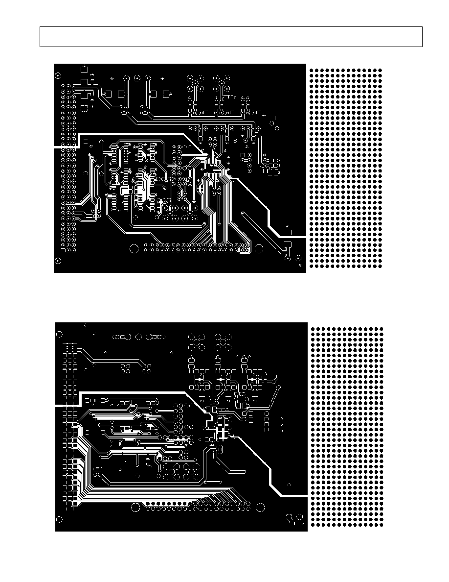
Figure 10. Component Side Artwork
Figure 11. Solder Side Artwork
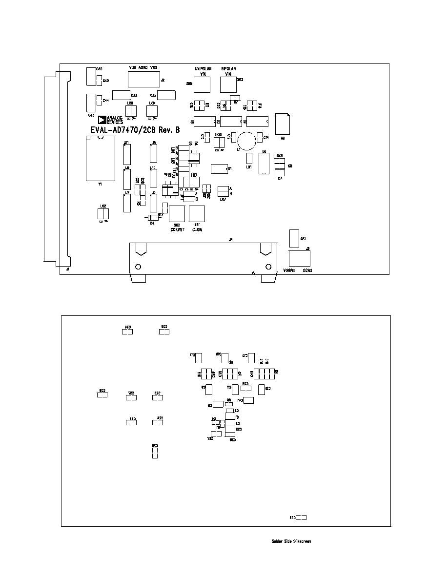
Figure 12. AD7470 Evaluation Board Component Placement Drawing (Component Side).
Figure 13. AD7470 Evaluation Board Component Placement Drawing (Solder Side).