Äîêóìåíòàöèÿ è îïèñàíèÿ www.docs.chipfind.ru
REV. 0
Information furnished by Analog Devices is believed to be accurate and
reliable. However, no responsibility is assumed by Analog Devices for its
use, nor for any infringements of patents or other rights of third parties that
may result from its use. No license is granted by implication or otherwise
under any patent or patent rights of Analog Devices.
a
AD7708/AD7718
One Technology Way, P.O. Box 9106, Norwood, MA 02062-9106, U.S.A.
Tel: 781/329-4700
www.analog.com
Fax: 781/326-8703
© Analog Devices, Inc., 2001
8-/10-Channel, Low Voltage,
Low Power, - ADCs
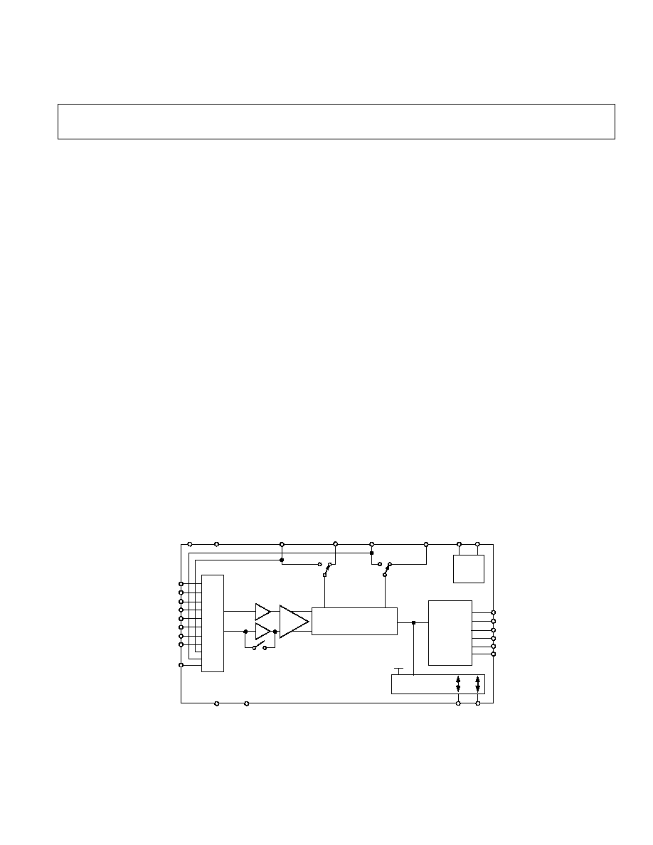
FUNCTIONAL BLOCK DIAGRAM
DVDD
XTAL1 XTAL2
MUX
POS BUF
- ADC*
AIN1
AIN2
AIN3
AIN4
PGA
OSC
AND
PLL
SERIAL
INTERFACE
AND
CONTROL
LOGIC
DOUT
DIN
SCLK
CS
RDY
RESET
AVDD
I/O PORT
AVDD
AD7708/ AD7718
DGND
P2
P1
REFIN2(+)/AIN9
REFIN1(+) REFIN2()/AIN10
REFIN1()
AINCOM
AIN5
AIN6
AIN7
AIN8
AGND
*AD7708 16-BIT ADC
*AD7718 24-BIT ADC
REFIN(+)
REFIN()
NEG BUF
FEATURES
8-/10-Channel, High Resolution - ADCs
AD7708 Has 16-Bit Resolution
AD7718 Has 24-Bit Resolution
Factory-Calibrated
Single Conversion Cycle Setting
Programmable Gain Front End
Simultaneous 50 Hz and 60 Hz Rejection
VREF SelectTM Allows Absolute and Ratiometric
Measurement Capability
Operation Can Be Optimized for
Analog Performance (
CHOP = 0) or
Channel Throughput (
CHOP = 1)
INTERFACE
3-Wire Serial
SPI
TM
, QSPI
TM
, MICROWIRE
TM
, and DSP-Compatible
Schmitt Trigger on SCLK
POWER
Specified for Single 3 V and 5 V Operation
Normal: 1.28 mA Typ @ 3 V
Power-Down: 30 A (32 kHz Crystal Running)
On-Chip Functions
Rail-to-Rail Input Buffer and PGA
2-Bit Digital I/O Port
APPLICATIONS
Industrial Process Control
Instrumentation
Pressure Transducers
Portable Instrumentation
Smart Transmitters
SPI and QSPI are trademarks of Motorola Inc.
MICROWIRE is a trademark of National Semiconductor Corp.
VREF Select is a trademark of Analog Devices, Inc.
GENERAL DESCRIPTION
The AD7708/AD7718 are complete analog front-ends for low
frequency measurement applications. The AD7718 contains a
24-bit
- ADC with PGA and can be configured as 4/5 fully-
differential input channels or 8/10 pseudo-differential input
channels. Two pins on the device are configurable as analog
inputs or reference inputs. The AD7708 is a 16-bit version of
the AD7718. Input signal ranges from 20 mV to 2.56 V can be
directly converted using these ADCs. Signals can be converted
directly from a transducer without the need for signal conditioning.
The device operates from a 32 kHz crystal with an on-board PLL
generating the required internal operating frequency. The output
data rate from the part is software programmable. The peak-to-
peak resolution from the part varies with the programmed gain
and output data rate.
The part operates from a single 3 V or 5 V supply. When operating
from 3 V supplies, the power dissipation for the part is 3.84 mW typ.
Both parts are pin-for-pin compatible allowing an upgradable
path from 16 to 24 bits without the need for hardware modifica-
tions. The AD7708/AD7718 are housed in 28-lead SOIC and
TSSOP packages.

REV. 0
2
AD7708/AD7718
FEATURES . . . . . . . . . . . . . . . . . . . . . . . . . . . . . . . . . . . . . 1
FUNCTIONAL BLOCK DIAGRAM . . . . . . . . . . . . . . . . . 1
GENERAL DESCRIPTION . . . . . . . . . . . . . . . . . . . . . . . . . 1
AD7718 SPECIFICATIONS . . . . . . . . . . . . . . . . . . . . . . . . 3
AD7708 SPECIFICATIONS . . . . . . . . . . . . . . . . . . . . . . . . 6
TIMING CHARACTERISTICS . . . . . . . . . . . . . . . . . . . . . 9
ABSOLUTE MAXIMUM RATINGS . . . . . . . . . . . . . . . . 10
ORDERING GUIDE . . . . . . . . . . . . . . . . . . . . . . . . . . . . . 10
PIN FUNCTION DESCRIPTIONS . . . . . . . . . . . . . . . . . 12
PIN CONFIGURATION . . . . . . . . . . . . . . . . . . . . . . . . . . 13
ADC CIRCUIT INFORMATION . . . . . . . . . . . . . . . . . . . 15
Signal Chain Overview (CHOP Enabled, CHOP = 0) . . . 15
ADC NOISE PERFORMANCE CHOP ENABLED
(
CHOP = 0) . . . . . . . . . . . . . . . . . . . . . . . . . . . . . . . . . . . 17
Signal Chain Overview (CHOP Disabled CHOP = 1) . . . 19
ADC NOISE PERFORMANCE CHOP DISABLED
(
CHOP = 1) . . . . . . . . . . . . . . . . . . . . . . . . . . . . . . . . . . . 20
ON-CHIP REGISTERS . . . . . . . . . . . . . . . . . . . . . . . . . . . 22
Communications Register . . . . . . . . . . . . . . . . . . . . . . . . . . 25
Status Register . . . . . . . . . . . . . . . . . . . . . . . . . . . . . . . . . . . 26
Mode Register . . . . . . . . . . . . . . . . . . . . . . . . . . . . . . . . . . . 27
Operating Characteristics when Addressing the
Mode and Control Registers . . . . . . . . . . . . . . . . . . . . . . . 28
ADC Control Register . . . . . . . . . . . . . . . . . . . . . . . . . . . . . 28
Filter Register . . . . . . . . . . . . . . . . . . . . . . . . . . . . . . . . . . . 29
I/O Control Register . . . . . . . . . . . . . . . . . . . . . . . . . . . . . . 30
ADC Data Result Register . . . . . . . . . . . . . . . . . . . . . . . . . . 30
Unipolar Mode . . . . . . . . . . . . . . . . . . . . . . . . . . . . . . . . . . 30
Bipolar Mode . . . . . . . . . . . . . . . . . . . . . . . . . . . . . . . . . . . . 31
ADC Offset Calibration Coefficient Registers . . . . . . . . . . . 31
ADC Gain Calibration Coefficient Register . . . . . . . . . . . . . 31
ID Register (ID) . . . . . . . . . . . . . . . . . . . . . . . . . . . . . . . . . 31
User Nonprogrammable Test Registers . . . . . . . . . . . . . . . . 31
Configuring the AD7708/AD7718 . . . . . . . . . . . . . . . . . . . . 32
DIGITAL INTERFACE . . . . . . . . . . . . . . . . . . . . . . . . . . . 34
MICROCOMPUTER/MICROPROCESSOR
INTERFACING . . . . . . . . . . . . . . . . . . . . . . . . . . . . . . . 34
AD7708/AD7718 to 68HC11 Interface . . . . . . . . . . . . . . . . 34
AD7708/AD7718-to-8051 Interface . . . . . . . . . . . . . . . . . . 35
AD7708/AD7718-to-ADSP-2103/ADSP-2105 Interface . . . 36
BASIC CONFIGURATION . . . . . . . . . . . . . . . . . . . . . . . . 36
Analog Input Channels . . . . . . . . . . . . . . . . . . . . . . . . . . . . 37
Single-Ended Operation . . . . . . . . . . . . . . . . . . . . . . . . . . . 37
Chop Mode of Operation (CHOP = 0) . . . . . . . . . . . . . . . . 37
Nonchop Mode of Operation (CHOP = 1) . . . . . . . . . . . . . 38
Programmable Gain Amplifier . . . . . . . . . . . . . . . . . . . . . . . 38
Bipolar/Unipolar Configuration . . . . . . . . . . . . . . . . . . . . . . 38
Data Output Coding . . . . . . . . . . . . . . . . . . . . . . . . . . . . . . 38
Oscillator Circuit . . . . . . . . . . . . . . . . . . . . . . . . . . . . . . . . . 39
Reference Input . . . . . . . . . . . . . . . . . . . . . . . . . . . . . . . . . . 39
RESET Input . . . . . . . . . . . . . . . . . . . . . . . . . . . . . . . . . . . 39
Power-Down Mode . . . . . . . . . . . . . . . . . . . . . . . . . . . . . . . 39
Calibration . . . . . . . . . . . . . . . . . . . . . . . . . . . . . . . . . . . . . . 40
Grounding and Layout . . . . . . . . . . . . . . . . . . . . . . . . . . . . 40
APPLICATIONS . . . . . . . . . . . . . . . . . . . . . . . . . . . . . . . . 41
Data Acquisition . . . . . . . . . . . . . . . . . . . . . . . . . . . . . . . . . 41
Programmable Logic Controllers . . . . . . . . . . . . . . . . . . . . . 41
Converting Single-Ended Inputs. . . . . . . . . . . . . . . . . . . . . 42
Combined Ratiometric and Absolute Value
Measurement System . . . . . . . . . . . . . . . . . . . . . . . . . . . . 42
Optimizing Throughput while Maximizing 50 Hz
and 60 Hz Rejection in a Multiplexed Data
Acquisition System . . . . . . . . . . . . . . . . . . . . . . . . . . . . . . 43
OUTLINE DIMENSIONS . . . . . . . . . . . . . . . . . . . . . . . . . 44
TABLE OF CONTENTS

REV. 0
3
AD7708/AD7718
Parameter
B Grade
Unit
Test Conditions
AD7718 (CHOP DISABLED)
Output Update Rate
16.06
Hz min
CHOP = 1
1.365
kHz max
No Missing Codes
2
24
Bits min
Resolution
13
Bits p-p
±20 mV Range, SF = 69
18
Bits p-p
±2.56 V Range, SF = 69
Output Noise and Update Rates
See Tables in
ADC Description
Integral Nonlinearity
±10
ppm of FSR max
2 ppm Typical
Offset Error
3
Table VII
µV typ
Offset Error is in the order of the noise for the
programmed gain and update rate following a
calibration
Offset Error Drift vs. Temp
4
±200
nV/
°C typ
Full-Scale Error
3
±10
µV typ
Gain Drift vs. Temp
4
±0.5
ppm/
°C typ
Negative Full-Scale Error
±0.003
% FSR max
ANALOG INPUTS
Differential Input Full-Scale Voltage
±1.024 × REFIN/GAIN V nom
REFIN Refers to Both REFIN1 and
REFIN2. REFIN = REFIN(+) REFIN()
GAIN = 1 to 128
Absolute AIN Voltage Limits
AGND + 100 mV
V min
AIN1AIN10 and AINCOM with
AV
DD
100 mV
V max
NEGBUF = 1
Absolute AINCOM Voltage Limits
AGND 30 mV
V min
NEGBUF = 0
AV
DD
+ 30 mV
V max
Analog Input Current
AIN1AIN10 and AINCOM with NEGBUF = 1
DC Input Current
2
±1
nA max
DC Bias Current Drift
±5
pA/
°C typ
AINCOM Input Current
NEGBUF = 0
DC Input Current
2
±125
nA/V typ
±2.56 V Range
DC Bias Current Drift
±2
pA/V/
°C typ
Normal-Mode Rejection
2
@ 50 Hz
100
dB min
50 Hz
± 1 Hz, SF Word = 82
@ 60 Hz
100
dB min
60 Hz
± 1 Hz, SF Word = 68
Common-Mode Rejection
@ DC
90
dB min
100 dB typ, Analog Input = 1 V,
Input Range =
±2.56 V
110 dB typ on
±20 mV Range
@ 50 Hz
100
dB typ
50 Hz
± 1 Hz, SF Word = 82
@ 60 Hz
100
dB typ
60 Hz
± 1 Hz, SF Word = 68
REFERENCE INPUTS (REFIN1 AND REFIN2)
REFIN(+) to REFIN() Voltage
2.5
V nom
REFIN Refers to Both REFIN1 and REFIN2
REFIN(+) to REFIN() Range
2
1
V min
AV
DD
V max
REFIN Common-Mode Range
AGND 30 mV
V min
AV
DD
+ 30 mV
V max
Reference DC Input Current
0.5
µA/V typ
Reference DC Input Current Drift
±0.1
nA/V/
°C typ
Normal-Mode Rejection
2
@ 50 Hz
100
dB min
50 Hz
± 1 Hz, SF Word = 82
@ 60 Hz
100
dB min
60 Hz
± 1 Hz, SF Word = 68
Common-Mode Rejection
Input Range =
±2.56 V
@ DC
100
dB typ
Analog Input = 1 V. Input Range =
±2.56 V
@ 50 Hz
100
dB typ
@ 60 Hz
100
dB typ
AD7718 SPECIFICATIONS
1
(AV
DD
= 2.7 V to 3.6 V or 4.75 V to 5.25 V, DV
DD
= 2.7 V to 3.6 V or 4.75 V to 5.25 V,
REFIN(+) = 2.5 V; REFIN() = AGND; AGND = DGND = 0 V; XTAL1/XTAL2 = 32.768 kHz Crystal Input Buffer Enabled. All specifications T
MIN
to
T
MAX
unless otherwise noted.)

REV. 0
4
AD7718SPECIFICATIONS
1
(AV
DD
= 2.7 V to 3.6 V or 4.75 V to 5.25 V, DV
DD
= 2.7 V to 3.6 V or 4.75 V to 5.25 V, REFIN(+) =
2.5 V ; REFIN() = AGND; AGND = DGND = 0 V; XTAL1/XTAL2 = 32.768 kHz Crystal Input Buffer Enabled. All specifications T
MIN
to T
MAX
unless otherwise noted.)
Parameter
B Grade
Unit
Test Conditions
AD7718 (CHOP ENABLED)
Output Update Rate
5.4
Hz min
CHOP = 0
105
Hz max
No Missing Codes
2
24
Bits min
20 Hz Update Rate
Resolution
13
Bits p-p
±20 mV Range, 20 Hz Update Rate
18
Bits p-p
±2.56 V Range, 20 Hz Update Rate
Output Noise and Update Rates
See Tables in
ADC Description
Integral Nonlinearity
±10
ppm of FSR max
2 ppm Typical
Offset Error
3
±3
µV typ
Offset Error Drift vs. Temp
4
10
nV/
°C typ
Full-Scale Error
3
±10
µV/°C typ
Gain Drift vs. Temp
4
±0.5
ppm/
°C typ
ANALOG INPUTS
Differential Input Full-Scale Voltage
±1.024 × REFIN/GAIN V nom
REFIN Refers to Both REFIN1 and
REFIN2. REFIN = REFIN(+) REFIN()
GAIN = 1 to 128
Range Matching
±2
µV typ
Analog Input = 18 mV
Absolute AIN Voltage Limits
AGND + 100 mV
V min
AIN1AIN10 and AINCOM with
AV
DD
100 mV
V max
NEGBUF = 1
Absolute AINCOM Voltage Limits
AGND 30 mV
V min
NEGBUF = 0
AV
DD
+ 30 mV
V max
Analog Input Current
AIN1AIN10 and AINCOM with
NEGBUF = 1
DC Input Current
2
±1
nA max
DC Input Current Drift
±5
pA/
°C typ
AINCOM Input Current
NEGBUF = 0
DC Input Current
2
±125
nA/V typ
±2.56 V Range
DC Bias Current Drift
±2
pA/V/
°C typ
Normal-Mode Rejection
2
@ 50 Hz
100
dB min
50 Hz
± 1 Hz, SF Word = 82
@ 60 Hz
100
dB min
60 Hz
± 1 Hz, SF Word = 68
Common-Mode Rejection
@ DC
90
dB min
100 dB typ, Analog Input = 1 V,
Input Range =
±2.56 V
110 dB typ on
±20 mV Range
@ 50 Hz
2
100
dB min
50 Hz
± 1 Hz, 20 Hz Update Rate
@ 60 Hz
2
100
dB min
60 Hz
± 1 Hz, 20 Hz Update Rate
REFERENCE INPUTS (REFIN1 AND REFIN2)
REFIN(+) to REFIN() Voltage
2.5
V nom
REFIN Refers to Both REFIN1 and
REFIN2
REFIN(+) to REFIN() Range
2
1
V min
AV
DD
V max
REFIN Common-Mode Range
AGND 30 mV
V min
AV
DD
+ 30 mV
V max
Reference DC Input Current
2
±0.5
µA/V typ
Reference DC Input Current Drift
±0.01
nA/V/
°C typ
Normal-Mode Rejection
2
@ 50 Hz
100
dB min
50 Hz
± 1 Hz, SF Word = 82
@ 60 Hz
100
dB min
60 Hz
± 1 Hz, SF Word = 68
Common-Mode Rejection
2
Input Range =
±2.56 V
@ DC
110
dB typ
Analog Input = 1 V
@ 50 Hz
110
dB typ
50 Hz
± 1 Hz, 20 Hz Update Rate
@ 60 Hz
110
dB typ
60 Hz
± 1 Hz, 20 Hz Update Rate
LOGIC INPUTS
5
All Inputs Except SCLK and XTAL1
2
V
INL
, Input Low Voltage
0.8
V max
DV
DD
= 5 V
V
INL
, Input Low Voltage
0.4
V max
DV
DD
= 3 V
V
INH
, Input High Voltage
2.0
V min
DV
DD
= 3 V or 5 V

REV. 0
5
AD7708/AD7718
Parameter
B Grade
Unit
Test Conditions
LOGIC INPUTS (Continued)
SCLK Only (Schmitt-Triggered Input)
2
V
T(+)
1.4/2
V min/V max
DV
DD
= 5 V
V
T()
0.8/1.4
V min/V max
DV
DD
= 5 V
V
T(+)
V
T()
0.3/0.85
V min/V max
DV
DD
= 5 V
V
T(+)
0.95/2
V min/V max
DV
DD
= 3 V
V
T()
0.4/1.1
V min/V max
DV
DD
= 3 V
V
T(+)
V
T()
0.3/0.85
V min/V max
DV
DD
= 3 V
XTAL1 Only
2
V
INL
, Input Low Voltage
0.8
V max
DV
DD
= 5 V
V
INH
, Input High Voltage
3.5
V min
DV
DD
= 5 V
V
INL
, Input Low Voltage
0.4
V max
DV
DD
= 3 V
V
INH
, Input High Voltage
2.5
V min
DV
DD
= 3 V
Input Currents
±10
µA max
Logic Input = DV
DD
70
µA max
Logic Input = DGND, Typical 40
µA @ 5 V
and 20
µA at 3 V
Input Capacitance
10
pF typ
All Digital Inputs
LOGIC OUTPUTS (Excluding XTAL2)
5
V
OH
, Output High Voltage
2
DV
DD
0.6
V min
DV
DD
= 3 V, I
SOURCE
= 100
µA
V
OL
, Output Low Voltage
2
0.4
V max
DV
DD
= 3 V, I
SINK
= 100
µA
V
OH
, Output High Voltage
2
4
V min
DV
DD
= 5 V, I
SOURCE
= 200
µA
V
OL
, Output Low Voltage
2
0.4
V max
DV
DD
= 5 V, I
SINK
= 1.6 mA
Floating State Leakage Current
±10
µA max
Floating State Output Capacitance
±10
pF typ
Data Output Coding
Binary
Unipolar Mode
Offset Binary
Bipolar Mode
SYSTEM CALIBRATION
2
Full-Scale Calibration Limit
1.05
× FS
V max
Zero-Scale Calibration Limit
1.05
× FS
V min
Input Span
0.8
× FS
V min
2.1
× FS
V max
START-UP TIME
From Power-On
300
ms typ
From Power-Down Mode
1
ms typ
Oscillator Enabled
300
ms typ
Oscillator Powered Down
POWER REQUIREMENTS
Power Supply Voltages
AV
DD
and DV
DD
can be operated independently of each other.
AV
DD
AGND
2.7/3.6
V min/max
AV
DD
= 3 V nom
4.75/5.25
V min/max
AV
DD
= 5 V nom
DV
DD
DGND
2.7/3.6
V min/max
DV
DD
= 3 V nom
4.75/5.25
V min
DV
DD
= 5 V nom
DI
DD
(Normal Mode)
0.55
mA max
DV
DD
= 3 V, 0.43 mA typ
0.65
mA max
DV
DD
= 5 V, 0.5 mA typ
AI
DD
(Normal Mode)
1.1
mA max
AV
DD
= 3 V or 5 V, 0.85 mA typ
DI
DD
(Power-Down Mode)
10
µA max
DV
DD
= 3 V, 32.768 kHz Osc. Running
2
µA max
DV
DD
= 3 V, Oscillator Powered Down
30
µA max
DV
DD
= 5 V, 32.768 kHz Osc. Running
8
µA max
DV
DD
= 5 V, Oscillator Powered Down
AI
DD
(Power-Down Mode)
1
µA max
AV
DD
= 3 V or 5 V
Power Supply Rejection (PSR)
Input Range =
±2.56 V, AIN = 1 V
Chop Disabled
70
dB min
95 dB typ
Chop Enabled
100
dB typ
NOTES
1
Temperature range is 40
°C to +85°C.
2
Not production tested, guaranteed by design and/or characterization data at release.
3
Following a self-calibration this error will be in the order of the noise for the programmed gain and update selected. A system calibration will completely remove this error.
4
Recalibration at any temperature will remove these errors.
5
I/O Port Logic Levels are with respect to AV
DD
and
AGND.
Specifications are subject to change without notice.
REV. 0
6
AD7708/AD7718
AD7708 SPECIFICATIONS
1
(AV
DD
= 2.7 V to 3.6 V or 4.75 V to 5.25 V, DV
DD
= 2.7 V to 3.6 V or 4.75 V to 5.25 V,
REFIN(+) = 2.5 V; REFIN() = AGND; AGND = DGND = 0 V; XTAL1/XTAL2 = 32.768 kHz Crystal Input Buffers Enabled. All specifications T
MIN
to
T
MAX
unless otherwise noted.)
Parameter
B Grade
Unit
Test Conditions
AD7708 (CHOP DISABLED)
Output Update Rate
16.06
Hz min
CHOP = 1
1.365
kHz max
No Missing Codes
2
16
Bits min
Resolution
13
Bits p-p
±20 mV Range, SF Word = 69
16
Bits p-p
±2.56 V Range, SF Word = 69
Output Noise and Update Rates
See Tables in ADC Description
Integral Nonlinearity
±15
ppm of FSR max
2ppm Typical
Offset Error
3
±0.65
LSB typ
Following a Self-Calibration
Offset Error Drift vs. Temp
4
±200
nV/
°C typ
Full-Scale Error
3
±0.75
LSB typ
Gain Drift vs. Temp
4
±0.5
ppm/
°C typ
Negative Full-Scale Error
±0.003
% FSR typ
ANALOG INPUTS
Differential Input Full-Scale Voltage
±1.024 × REFIN/GAIN V nom
REFIN Refers to Both REFIN1 and
REFIN2. REFIN = REFIN(+) REFIN()
GAIN = 1 to 128
Absolute AIN Voltage Limits
AGND + 100 mV
V min
AIN1AIN10 and AINCOM with
AV
DD
100 mV
V max
NEGBUF = 1
Absolute AINCOM Voltage Limits
AGND 30 mV
V min
NEGBUF = 0
AV
DD
+ 30 mV
V max
Analog Input Current
AIN1AIN10 and AINCOM with
NEGBUF = 1
DC Input Current
2
±1
nA max
DC Bias Current Drift
±5
pA/
°C typ
AINCOM Input Current
NEGBUF = 0
DC Input Current
2
±125
nA/V typ
±2.56 V Range
DC Bias Current Drift
±2
pA/V/
°C typ
Normal-Mode Rejection
2
@ 50 Hz
100
dB min
50 Hz
± 1 Hz, SF Word = 82
@ 60 Hz
100
dB min
60 Hz
± 1 Hz, SF Word = 68
Common-Mode Rejection
@ DC
90
dB min
100 dB typ, Analog Input = 1 V,
Input Range =
±2.56 V
110 dB typ on
±20 mV Range
@ 50 Hz
100
dB typ
50 Hz
± 1 Hz, SF Word = 82
@ 60 Hz
100
dB typ
60 Hz
± 1 Hz, SF Word = 68
REFERENCE INPUTS (REFIN1 AND REFIN2)
REFIN(+) to REFIN() Voltage
2.5
V nom
REFIN Refers to Both REFIN1 and
REFIN2
REFIN(+) to REFIN() Range
2
1
V min
AV
DD
V max
REFIN Common-Mode Range
AGND 30 mV
V min
AV
DD
+ 30 mV
V max
Reference DC Input Current
0.5
µA/V typ
Reference DC Input Current Drift
±0.1
nA/V/
°C typ
Normal-Mode Rejection
2
@ 50 Hz
100
dB min
50 Hz
± 1 Hz, SF Word = 82
@ 60 Hz
100
dB min
60 Hz
± 1 Hz, SF Word = 68
Common-Mode Rejection
Input Range =
±2.56 V
@ DC
100
dB typ
Analog Input = 1 V. Input Range =
±2.56 V
@ 50 Hz
100
dB typ
@ 60 Hz
100
dB typ

REV. 0
7
AD7708/AD7718
Parameter
B Grade
Unit
Test Conditions
AD7708 (CHOP ENABLED)
Output Update Rate
5.4
Hz min
CHOP = 1
105
Hz max
0.732 ms Increments
No Missing Codes
2
16
Bits min
20 Hz Update Rate
Resolution
13
Bits p-p
±20 mV Range, 20 Hz Update Rate
16
Bits p-p
±2.56 V Range, 20 Hz Update Rate
Output Noise and Update Rates
See Tables in
ADC Description
Integral Nonlinearity
±15
ppm of FSR max
2 ppm Typical
Offset Error
3
±3
µV typ
Calibration is Accurate to
±0.5 LSB
Offset Error Drift vs. Temp
4
10
nV/
°C typ
Full-Scale Error
3
±0.75
LSB typ
Includes Positive and Negative ERRORS
Gain Drift vs. Temp
4
±0.5
ppm/
°C typ
ANALOG INPUTS
Differential Input Full-Scale Voltage
±1.024 × REFIN/GAIN V nom
REFIN Refers to Both REFIN1 and
REFIN2. REFIN = REFIN(+) REFIN()
GAIN = 1 to 128
Range Matching
±2
µV typ
Analog Input = 18 mV
Absolute AIN Voltage Limits
AGND + 100 mV
V min
AIN1AIN10 and AINCOM with
AV
DD
100 mV
V max
NEGBUF = 1
Absolute AINCOM Voltage Limits
AGND 30 mV
V min
NEGBUF = 0
AV
DD
+ 30 mV
V max
Analog Input Current
AIN1AIN10 and AINCOM with
NEGBUF = 1
DC Input Current
2
±1
nA max
DC Input Current Drift
±5
pA/
°C typ
AINCOM Input Current
NEGBUF = 0
DC Input Current
2
±125
nA/V typ
DC Bias Current Drift
±2
pA/V/
°C typ
Normal-Mode Rejection
2
@ 50 Hz
100
dB min
50 Hz
± 1 Hz, SF Word = 82
@ 60 Hz
94
dB min
60 Hz
± 1 Hz, SF Word = 68
Common-Mode Rejection
@ DC
90
dB min
100 dB typ, Analog Input = 1 V,
Input Range =
±2.56 V
110 dB typ on
±20 mV Range
@ 50 Hz
2
100
dB min
50 Hz
± 1 Hz, 20 Hz Update Rate
@ 60 Hz
2
100
dB min
60 Hz
± 1 Hz, 20 Hz Update Rate
REFERENCE INPUTS (REFIN1 AND REFIN2)
REFIN(+) to REFIN() Voltage
2.5 V
nom
REFIN Refers to Both REFIN1 and
REFIN2
REFIN(+) to REFIN() Range
2
1
V min
AV
DD
V max
REFIN Common-Mode Range
AGND 30 mV
V min
AV
DD
+ 30 mV
V max
Reference DC Input Current
2
±0.5
µA/V typ
Reference DC Input Current Drift
±0.01
nA/V/
°C typ
Normal-Mode Rejection
2
@ 50 Hz
100
dB min
50 Hz
± 1 Hz, SF Word = 82
@ 60 Hz
100
dB min
60 Hz
± 1 Hz, SF Word = 68
Common-Mode Rejection
Input Range =
±2.56 V
@ DC
110
dB typ
Analog Input = 1 V
@ 50 Hz
110
dB typ
50 Hz
± 1 Hz, 20 Hz Update Rate
@ 60 Hz
110
dB typ
60 Hz
± 1 Hz, 20 Hz Update Rate
LOGIC INPUTS
5
All Inputs Except SCLK and XTAL1
2
V
INL
, Input Low Voltage
0.8
V max
DV
DD
= 5 V
0.4
V max
DV
DD
= 3 V
V
INH
, Input High Voltage
2.0
V min
DV
DD
= 3 V or 5 V

REV. 0
8
AD7718SPECIFICATIONS
1
(AV
DD
= 2.7 V to 3.6 V or 4.75 V to 5.25 V, DV
DD
= 2.7 V to 3.6 V or 4.75 V to 5.25 V, REFIN(+) =
2.5 V ; REFIN() = AGND; AGND = DGND = 0 V; XTAL1/XTAL2 = 32.768 kHz Crystal Input Buffer Enabled. All specifications T
MIN
to T
MAX
unless otherwise noted.)
AD7708
Parameter
B Grade
Unit
Test Conditions
LOGIC INPUTS (Continued)
SCLK Only (Schmitt-Triggered Input)
2
V
T(+)
1.4/2
V min/V max
DV
DD
= 5 V
V
T()
0.8/1.4
V min/V max
DV
DD
= 5 V
V
T(+)
V
T()
0.3/0.85
V min/V max
DV
DD
= 5 V
V
T(+)
0.95/2
V min/V max
DV
DD
= 3 V
V
T()
0.4/1.1
V min/V max
DV
DD
= 3 V
V
T(+)
V
T()
0.3/0.85
V min/V max
DV
DD
= 3 V
XTAL1 Only
2
V
INL
, Input Low Voltage
0.8
V max
DV
DD
= 5 V
V
INH
, Input High Voltage
3.5
V min
DV
DD
= 5 V
V
INL
, Input Low Voltage
0.4
V max
DV
DD
= 3 V
V
INH
, Input High Voltage
2.5
V min
DV
DD
= 3 V
Input Currents
±10
µA max
Logic Input = DV
DD
70
µA max
Logic Input = DGND, Typical 40
µA @ 5 V
and 20
µA at 3 V
Input Capacitance
10
pF typ
All Digital Inputs
LOGIC OUTPUTS (Excluding XTAL2)
5
V
OH
, Output High Voltage
2
DV
DD
0.6
V min
DV
DD
= 3 V, I
SOURCE
= 100
µA
V
OL
, Output Low Voltage
2
0.4
V max
DV
DD
= 3 V, I
SINK
= 100
µA
V
OH
, Output High Voltage
2
4
V min
DV
DD
= 5 V, I
SOURCE
= 200
µA
V
OL
, Output Low Voltage
2
0.4
V max
DV
DD
= 5 V, I
SINK
= 1.6 mA
Floating State Leakage Current
±10
µA max
Floating State Output Capacitance
±10
pF typ
Data Output Coding
Binary
Unipolar Mode
Offset Binary
Bipolar Mode
SYSTEM CALIBRATION
2
Full-Scale Calibration Limit
1.05
× FS
V max
Zero-Scale Calibration Limit
1.05
× FS
V min
Input Span
0.8
× FS
V min
2.1
× FS
V max
START-UP TIME
From Power-On
300
ms typ
From Power-Down Mode
1
ms typ
300
ms typ
Oscillator Powered Down
POWER REQUIREMENTS
Power Supply Voltages
AV
DD
and DV
DD
can be operated independently of each other.
AV
DD
AGND
2.7/3.6
V min/max
AV
DD
= 3 V nom
4.75/5.25
V min/max
AV
DD
= 5 V nom
DV
DD
DGND
2.7/3.6
V min/max
DV
DD
= 3 V nom
4.75/5.25
V min
DV
DD
= 5 V nom
DI
DD
(Normal Mode)
0.55
mA max
DV
DD
= 3 V, 0.43 mA typ
0.65
mA
DV
DD
= 5 V, 0.5 mA typ
AI
DD
(Normal Mode)
1.1
mA
AV
DD
= 3 V or 5 V, 0.85 mA typ
DI
DD
(Power-Down Mode)
10
µA max
DV
DD
= 3 V, 32.768 kHz Osc. Running
2
µA max
DV
DD
= 3 V, Oscillator Powered Down
30
µA max
DV
DD
= 5 V, 32.768 kHz Osc. Running
8
µA max
DV
DD
= 5 V, Oscillator Powered Down
AI
DD
(Power-Down Mode)
1
µA max
AV
DD
= 3 V or 5 V
Power Supply Rejection (PSR)
Input Range =
±2.56 V, AIN = 1 V
Chop Disabled
70
dB min
95 dB typ
Chop Enabled
100
dB typ
NOTES
1
Temperature range is 40
°C to +85°C.
2
Not production tested, guaranteed by design and/or characterization data at release.
3
Following a self-calibration this error will be in the order of the noise for the programmed gain and update selected. A system calibration will completely
remove this error.
4
Recalibration at any temperature will remove these errors.
5
I/O Port Logic Levels are with respect to AV
DD
and
AGND.
Specifications are subject to change without notice.
REV. 0
AD7708/AD7718
9
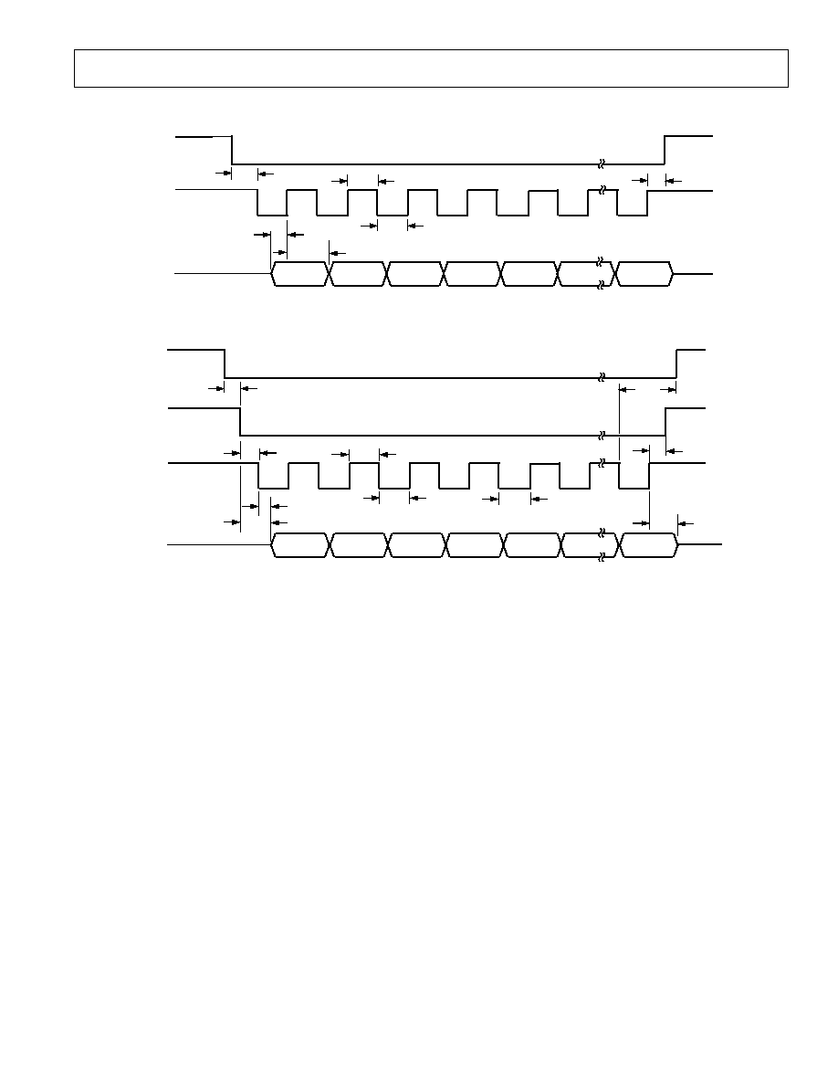
TIMING CHARACTERISTICS
1, 2
(AV
DD
= 2.7 V to 3.6 V or AV
DD
= 5 V 5%; DV
DD
= 2.7 V to 3.6 V or DV
DD
= 5 V 5%; AGND =
DGND = 0 V; XTAL = 32.768 kHz; Input Logic 0 = 0 V, Logic 1 = DV
DD
unless otherwise noted.
Limit at T
MIN
, T
MAX
Parameter
(B Version)
Unit
Conditions/Comments
t
1
32.768
kHz typ
Crystal Oscillator Frequency
t
2
50
ns min
RESET Pulsewidth
Read Operation
t
3
0
ns min
RDY to CS Setup Time
t
4
0
ns min
CS Falling Edge to SCLK Active Edge Setup Time
3
t
5
4
0
ns min
SCLK Active Edge to Data Valid Delay
3
60
ns max
DV
DD
= 4.5 V to 5.5 V
80
ns max
DV
DD
= 2.7 V to 3.6 V
t
5A
4, 5
0
ns min
CS Falling Edge to Data Valid Delay
3
60
ns max
DV
DD
= 4.5 V to 5.5 V
80
ns max
DV
DD
= 2.7 V to 3.6 V
t
6
100
ns min
SCLK High Pulsewidth
t
7
100
ns min
SCLK Low Pulsewidth
t
8
0
ns min
CS Rising Edge to SCLK Inactive Edge Hold Time
3
t
9
6
10
ns min
Bus Relinquish Time after SCLK Inactive Edge
3
80
ns max
t
10
100
ns max
SCLK Active Edge to
RDY High
3, 7
Write Operation
t
11
0
ns min
CS Falling Edge to SCLK Active Edge Setup Time
3
t
12
30
ns min
Data Valid to SCLK Edge Setup Time
t
13
25
ns min
Data Valid to SCLK Edge Hold Time
t
14
100
ns min
SCLK High Pulsewidth
t
15
100
ns min
SCLK Low Pulsewidth
t
16
0
ns min
CS Rising Edge to SCLK Edge Hold Time
NOTES
1
Sample tested during initial release to ensure compliance. All input signals are specified with tr = tf = 5 ns (10% to 90% of DV
DD
) and timed from a voltage
level of 1.6 V.
2
See Figures 1 and 2.
3
SCLK active edge is falling edge of SCLK.
4
These numbers are measured with the load circuit of Figure 1 and defined as the time required for the output to cross the V
OL
or V
OH
limits.
5
This specification only comes into play if CS goes low while SCLK is low. It is required primarily for interfacing to DSP machines.
6
These numbers are derived from the measured time taken by the data output to change 0.5 V when loaded with the load circuit of Figure 1. The measured number is
then extrapolated back to remove effects of charging or discharging the 50 pF capacitor. This means that the times quoted in the timing characteristics are the true
bus relinquish times of the part and as such are independent of external bus loading capacitances.
7
RDY returns high after the first read from the device after an output update. The same data can be read again, if required, while RDY is high, although care should
be taken that subsequent reads do not occur close to the next output update.
Specifications subject to change without notice.
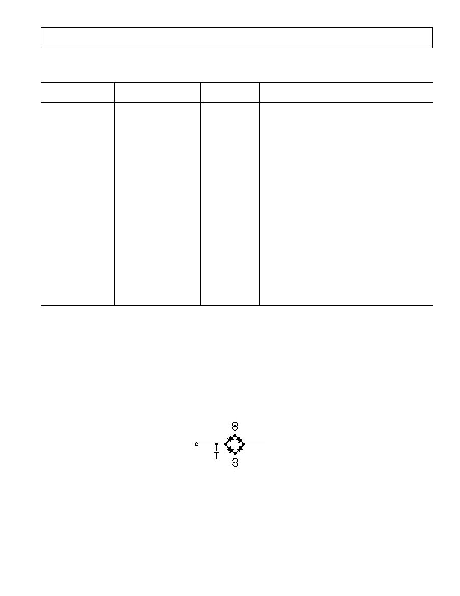
TO OUTPUT
PIN
50pF
I
SINK
I
SOURCE
1.6V
(1.6mA WITH DV
DD
= 5V
100 A WITH DV
DD
= 3V)
(200 A WITH DV
DD
= 5V
100 A WITH DV
DD
= 3V)
Figure 1. Load Circuit for Timing Characterization
REV. 0
10
AD7708/AD7718
ABSOLUTE MAXIMUM RATINGS
*
(T
A
= 25
°C unless otherwise noted)
AV
DD
to AGND . . . . . . . . . . . . . . . . . . . . . . . 0.3 V to +7 V
AV
DD
to DGND . . . . . . . . . . . . . . . . . . . . . . . 0.3 V to +7 V
DV
DD
to AGND . . . . . . . . . . . . . . . . . . . . . . . 0.3 V to +7 V
DV
DD
to DGND . . . . . . . . . . . . . . . . . . . . . . . 0.3 V to +7 V
AGND to DGND . . . . . . . . . . . . . . . . . . 0.05 V to +0.05 V
AV
DD
to DV
DD
. . . . . . . . . . . . . . . . . . . . . . . . . 5 V to +5 V
Analog Input Voltage to AGND . . . . 0.3 V to AV
DD
+0.3 V
Reference Input Voltage to AGND . . 0.3 V to AV
DD
+0.3 V
Total AIN/REFIN Current (Indefinite) . . . . . . . . . . . . 30 mA
Digital Input Voltage to DGND . . . . 0.3 V to DV
DD
+0.3 V
Digital Output Voltage to DGND . . . 0.3 V to DV
DD
+0.3 V
Operating Temperature Range . . . . . . . . . . . 40
°C to +85°C
Storage Temperature Range . . . . . . . . . . . . 65
°C to +150°C
Junction Temperature . . . . . . . . . . . . . . . . . . . . . . . . . 150
°C
SOIC Package
JA
Thermal Impedance . . . . . . . . . . . . . . . . . . . 71.4
°C/W
JC
Thermal Impedance . . . . . . . . . . . . . . . . . . . . . 23
°C/W
TSSOP Package
JA
Thermal Impedance . . . . . . . . . . . . . . . . . . . 97.9
°C/W
JC
Thermal Impedance . . . . . . . . . . . . . . . . . . . . . 14
°C/W
Lead Temperature, Soldering
Vapor Phase (60 sec) . . . . . . . . . . . . . . . . . . . . . . . . 215
°C
Infrared (15 sec) . . . . . . . . . . . . . . . . . . . . . . . . . . . . 220
°C
*Stresses above those listed under Absolute Maximum Ratings may cause perma-
nent damage to the device. This is a stress rating only; functional operation of the
device at these or any other conditions above those listed in the operational
sections of this specification is not implied. Exposure to absolute maximum rating
conditions for extended periods may affect device reliability.
CAUTION
ESD (electrostatic discharge) sensitive device. Electrostatic charges as high as 4000 V readily
accumulate on the human body and test equipment and can discharge without detection. Although
the AD7708/AD7718 features proprietary ESD protection circuitry, permanent damage may occur
on devices subjected to high-energy electrostatic discharges. Therefore, proper ESD precautions
are recommended to avoid performance degradation or loss of functionality.
WARNING!
ESD SENSITIVE DEVICE
ORDERING GUIDE
Temperature
Package
Package
Model
Range
Description Option
AD7708BR
40
°C to +85°C SOIC
R-28
AD7708BRU
40
°C to +85°C TSSOP
RU-28
EVAL-AD7708EB
Evaluation Board
AD7718BR
40
°C to +85°C SOIC
R-28
AD7718BRU
40
°C to +85°C TSSOP
RU-28
EVAL-AD7718EB
Evaluation Board
REV. 0
AD7708/AD7718
11
t
12
t
13
t
14
t
15
t
11
t
16
MSB
LSB
CS
SCLK
DIN
Figure 2. Write Cycle Timing Diagram
t
5
t
5A
t
4
t
6
t
3
t
9
MSB
LSB
CS
SCLK
t
8
t
10
t
7
t
6
DOUT
RDY
Figure 3. Read Cycle Timing Diagram

REV. 0
12
AD7708/AD7718
PIN FUNCTION DESCRIPTIONS
Pin No
Mnemonic
Function
1
AIN7
Analog Input Channel 7. Programmable-gain analog input that can be used as a pseudo-
differential input when used with AINCOM, or as the positive input of a fully-differential input
pair when used with AIN8. (See ADC Control Register section.)
2
AIN8
Analog Input Channel 8. Programmable-gain analog input that can be used as a pseudo-
differential input when used with AINCOM, or as the negative input of a fully-differential input
pair when used with AIN7. (See ADC Control Register section.)
3
AV
DD
Analog Supply Voltage
4
AGND
Analog Ground
5
REFIN1()
Negative Reference Input. This reference input can lie anywhere between AGND and AV
DD
1 V.
6
REFIN1(+)
Positive reference input. REFIN(+) can lie anywhere between AV
DD
and AGND. The nominal
reference voltage [REFIN(+)REFIN()] is 2.5 V but the part is functional with a reference
range from 1 V to AV
DD
.
7
AIN1
Analog Input Channel 1. Programmable-gain analog input that can be used as a pseudo-
differential input when used with AINCOM, or as the positive input of a fully-differential input
pair when used with AIN2. (See ADC Control Register Section.)
8
AIN2
Analog Input Channel 2. Programmable-gain analog input that can be used as a pseudo-
differential input when used with AINCOM, or as the negative input of a fully-differential input
pair when used with AIN1. (See ADC Control Register section.)
9
AIN3
Analog Input Channel 3. Programmable-gain analog input that can be used as a pseudo-
differential input when used with AINCOM, or as the positive input of a fully-differential input
pair when used with AIN4. (See ADC Control Register section.)
10
AIN4
Analog Input Channel 4. Programmable-gain analog input that can be used as a pseudo-
differential input when used with AINCOM, or as the negative input of a fully-differential input
pair when used with AIN3. (See ADC Control Register section.)
11
AIN5
Analog Input Channel 5. Programmable-gain analog input that can be used as a pseudo-
differential input when used with AINCOM, or as the positive input of a fully-differential input
pair when used with AIN6. (See ADC Control Register section ADCCON.)
12
AINCOM
All analog inputs are referenced to this input when configured in pseudo-differential input mode.
13
REFIN2(+)/AIN9
Positive reference input/analog input. This input can be configured as a reference input with the
same characteristics as REFIN1(+) or as an additional analog input. When configured as an
analog input this pin provides a programmable-gain analog input that can be used as a pseudo-
differential input when used with AINCOM, or as the positive input of a fully-differential input
pair when used with AIN10. (See ADC Control Register section.)
14
REFIN2()/AIN10
Negative reference input/analog input. This pin can be configured as a reference or analog input.
When configured as a reference input it provides the negative reference input for REFIN2.
When configured as an analog input it provides a programmable-gain analog input that can be
used as a pseudo-differential input when used with AINCOM, or as the negative input of a fully-
differential input pair when used with AIN9. (See ADC Control Register section.)
15
AIN6
Analog Input Channel 6. Programmable-gain analog input that can be used as a pseudo-
differential input when used with AINCOM, or as the negative input of a fully-differential input
pair when used with AIN5. (See ADC Control Register section.)
16
P2
P2 can act as a general-purpose Input/Output bit referenced between AV
DD
and AGND. There
is a weak pull-up to AV
DD
internally on this pin.
17
AGND
It is recommended that this pin be tied directly to AGND.
18
P1
P1 can act as a general-purpose Input/Output bit referenced between AV
DD
and AGND. There
is a weak pull-up to AV
DD
internally on this pin.
19
RESET
Digital input used to reset the ADC to its power-on-reset status. This pin has a weak pull-up
internally to DV
DD
.
20
SCLK
Serial clock input for data transfers to and from the ADC. The SCLK has a Schmitt-trigger
input making an opto-isolated interface more robust. The serial clock can be continuous with all
data transmitted in a continuous train of pulses. Alternatively, it can be a noncontinuous clock
with the information being transmitted to or from the AD7708/AD7718 in smaller batches of data.
REV. 0
AD7708/AD7718
13
Pin No
Mnemonic
Function
21
CS
Chip Select Input. This is an active low logic input used to select the AD7708/AD7718.
CS can
be used to select the AD7708/AD7718 in systems with more than one device on the serial bus or
as a frame synchronization signal in communicating with the device.
CS can be hardwired low,
allowing the AD7708/AD7718 to be operated in 3-wire mode with SCLK, DIN, and DOUT
used to interface with the device.
22
RDY
RDY is a logic low status output from the AD7708/AD7718. RDY is low when valid data exists
in the data register for the selected channel. This output returns high on completion of a read
operation from the data register. If data is not read,
RDY will return high prior to the next update
indicating to the user that a read operation should not be initiated. The
RDY pin also returns
low following the completion of a calibration cycle.
RDY does not return high after a calibration
until the mode bits are written to enabling a new conversion or calibration.
23
DOUT
Serial data output with serial data being read from the output shift register of the ADC. The output
shift register can contain data from any of the on-chip data, calibration or control registers.
24
DIN
Serial Data Input with serial data being written to the input shift register on the AD7708/AD7718
Data in this shift register is transferred to the calibration or control registers within the ADC
depending on the selection bits of the Communications register.
25
DGND
Ground Reference Point for the Digital Circuitry.
26
DV
DD
Digital Supply Voltage, 3 V or 5 V Nominal.
27
XTAL2
Output from the 32 kHz Crystal Oscillator or Resonator Inverter.
28
XTAL1
Input to the 32 kHz Crystal Oscillator or Resonator Inverter.
PIN CONFIGURATION
14
13
12
11
17
16
15
20
19
18
10
9
8
1
2
3
4
7
6
5
TOP VIEW
(Not to Scale)
28
27
26
25
24
23
22
21
AD7708/
AD7718
AIN7
DGND
DV
DD
XTAL2
XTAL1
AIN8
AV
DD
AGND
RDY
DOUT
DIN
REFIN1()
REFIN1(+)
AIN1
AIN2
AIN3
AIN4
RESET
SCLK
CS
AIN5
AINCOM
REFIN2(+)/AIN9
REFIN2()/AIN10
P1
AIN6
P2
AGND
REV. 0
14
AD7708/AD7718
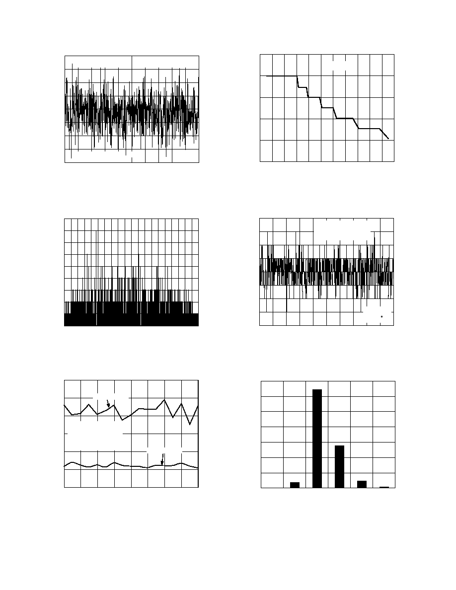
READING NUMBER
8389600
8389400
8388000
0
1000
100
CODE READ
200
300
8389200
400
500
600
700
800
900
8389000
8388800
8388600
8388400
8388200
AV
DD
= DV
DD
= 5V
INPUT RANGE = 20mV
REFIN1(+)REFIN1() = 2.5V
UPDATE RATE = 19.79Hz
T
A
= 25 C
V
REF
= 2.5V
RMS NOISE = 0.58 V rms
TPC 1. AD7718 Typical Noise Plot on
±20 mV Input Range
with 19.79 Hz Update Rate
8
7
0
8388039
8388721
8388687
8388657
8388615
8388579
8388547
8388499
8388449
8388382
8388754
8389110
8389033
8388985
8388941
8388906
8388874
8388841
8388805
8388779
6
5
4
3
2
1
9
TPC 2. AD7718 Noise Distribution Histogram
2.5
0
1.0
3.0
2.5
2.0
1.5
3.5
5.0
4.5
4.0
2.0
1.5
1.0
0.5
3.0
V
REF
V
RMS NOISE
V
20mV RANGE
2.56V RANGE
AV
DD
= DV
DD
= 5V
V
REF
= 2.5V
INPUT RANGE = 2.56V
UPDATE RATE = 19.79Hz
T
A
= 25 C
TPC 3. RMS Noise vs. Reference Input
(AD7718 andAD7708)
16
0
40
30
20
10
50
100
90
80
70
60
24
22
20
18
26
UPDATE RATE Hz
NO MISSING CODES
Min
110
CHOP = 0
TPC 4. AD7718 No-Missing Codes Performance
32767
100
0
200
400
300
32771
32770
32769
32768
32772
READING NUMBER
CODE READ
500
32766
32765
32764
600
700
800
900
1000
AV
DD
= DV
DD
= 5V
INPUT RANGE = 20mV
UPDATE RATE = 19.79Hz
V
REF
= 2.5V
T
A
= 25 C
TPC 5. AD7708 Typical Noise Plot on
±20 mV Input Range
200
32767
32766
32768
32770
32769
600
500
400
300
700
CODE
OCCURRENCE
32771
100
0
TPC 6. AD7708 Noise Histogram
Typical Performance Characteristics
REV. 0
AD7708/AD7718
15
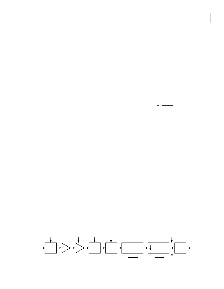
ADC CIRCUIT INFORMATION
The AD7708/AD7718 incorporates a 10-channel multiplexer
with a sigma-delta ADC, on-chip programmable gain amplifier
and digital filtering intended for the measurement of wide
dynamic range, low frequency signals such as those in weigh-scale,
strain-gauge, pressure transducer, or temperature measurement
applications. The AD7708 offers 16-bit resolution while the
AD7718 offers 24-bit resolution. The AD7718 is a pin-for-pin
compatible version of the AD7708. The AD7718 offers a direct
upgradable path from a 16-bit to a 24-bit system without requiring
any hardware changes and only minimal software changes.
These parts can be configured as four/five fully-differential
input channels or as eight/ten pseudo-differential input chan-
nels referenced to AINCOM. The channel is buffered and can
be programmed for one of eight input ranges from
±20 mV to
±2.56 V. Buffering the input channel means that the part can
handle significant source impedances on the analog input and
that R, C filtering (for noise rejection or RFI reduction) can be
placed on the analog inputs if required. These input channels
are intended to convert signals directly from sensors without the
need for external signal conditioning.
The ADC employs a sigma-delta conversion technique to realize
up to 24 bits of no missing codes performance. The sigma-delta
modulator converts the sampled input signal into a digital pulse
train whose duty cycle contains the digital information. A Sinc
3
programmable low-pass filter is then employed to decimate the
modulator output data stream to give a valid data conversion result
at programmable output rates. The signal chain has two modes
of operation, CHOP enabled and CHOP disabled. The
CHOP bit
in the mode register enables and disables the chopping scheme.
Signal Chain Overview (CHOP Enabled, CHOP = 0)
With CHOP = 0, chopping is enabled, this is the default and gives
optimum performance in terms of drift performance. With chopping
enabled, the available output rates vary from 5.35 Hz (186.77 ms)
to 105.03 Hz (9.52 ms). A block diagram of the ADC input
channel with chop enabled is shown in Figure 4.
The sampling frequency of the modulator loop is many times
higher than the bandwidth of the input signal. The integrator in
the modulator shapes the quantization noise (which results from
the analog-to-digital conversion) so that the noise is pushed
toward one-half of the modulator frequency. The output of the
sigma-delta modulator feeds directly into the digital filter. The
digital filter then band-limits the response to a frequency signifi-
cantly lower than one-half of the modulator frequency. In this
manner, the 1-bit output of the comparator is translated into a
band limited, low noise output from the AD7708/AD7718 ADC.
The AD7708/AD7718 filter is a low-pass, Sinc
3
or (sinx/x)
3
filter whose primary function is to remove the quantization noise
introduced at the modulator. The cutoff frequency and deci-
mated output data rate of the filter are programmable via the SF
word loaded to the filter register. The complete signal chain is
chopped resulting in excellent dc offset and offset drift specifica-
tions and is extremely beneficial in applications where drift, noise
rejection, and optimum EMI rejection are important factors.
With chopping, the ADC repeatedly reverses its inputs. The
decimated digital output words from the Sinc
3
filters, therefore,
have a positive offset and negative offset term included. As a
result, a final summing stage is included so that each output
word from the filter is summed and averaged with the previous
filter output to produce a new valid output result to be written
to the ADC data register. The programming of the Sinc
3
deci-
mation factor is restricted to an 8-bit register SF, the actual
decimation factor is the register value times 8. The decimated
output rate from the Sinc
3
filter (and the ADC conversion rate)
will therefore be
f
SF
f
ADC
MOD
= ×
×
×
1
3
1
8
where
f
ADC
in the ADC conversion rate.
SF is the decimal equivalent of the word loaded to the filter
register.
f
MOD
is the modulator sampling rate of 32.768 kHz.
The chop rate of the channel is half the output data rate:
f
f
CHOP
ADC
=
×
1
2
As shown in the block diagram, the Sinc
3
filter outputs alter-
nately contain +V
OS
and V
OS
, where V
OS
is the respective
channel offset. This offset is removed by performing a running
average of two. This average by two means that the settling time
to any change in programming of the ADC will be twice the
normal conversion time, while an asynchronous step change on
the analog input will not be fully reflected until the third subse-
quent output.
t
f
t
SETTLE
ADC
ADC
=
= ×
2
2
The allowable range for SF is 13 to 255 with a default of 69
(45H). The corresponding conversion rates, conversion times,
and settling times are shown in Table I. Note that the conver-
sion time increases by 0.732 ms for each increment in SF.
SINC
3
FILTER
MUX
BUF
PGA
-
MOD0
XOR
ANALOG
INPUT
DIGITAL
OUTPUT
1
8 SF
3
(8 SF )
3
1
2
A
IN
+ V
OS
A
IN
V
OS
f
CHOP
f
IN
f
MOD
f
CHOP
f
ADC
(
(
Figure 4. ADC Channel Block Diagram with CHOP Enabled
REV. 0
16
AD7708/AD7718
Table I. ADC Conversion and Settling Times for Various
SF Words with
CHOP = 0
SF
Data Update Rate
Settling Time
Word
f
ADC
(Hz)
t
SETTLE
(ms)
13
105.3
19.04
23
59.36
33.69
27
50.56
39.55
45
30.3
65.9
69 (Default)
19.79
101.07
91
15
133.1
182
7.5
266.6
255
5.35
373.54
The overall frequency response is the product of a sinc
3
and a
sinc response. There are sinc
3
notches at integer multiples of
3
× f
ADC
and there are sinc notches at odd integer multiples
of f
ADC
/2. The 3 dB frequency for all values of SF obeys the
following equation:
f (3 dB) = 0.24
× f
ADC
Normal-mode rejection is the major function of the digital filter
on the AD7708/AD7718. The normal mode 50
±1 Hz rejection
with an SF word of 82 is typically 100 dB. The 60
± 1 Hz
rejection with SF = 68 is typically 100 dB. Simultaneous 50 Hz
and 60 Hz rejection of better than 60 dB is achieved with an SF
of 69. Choosing an SF word of 69 places notches at both 50 Hz
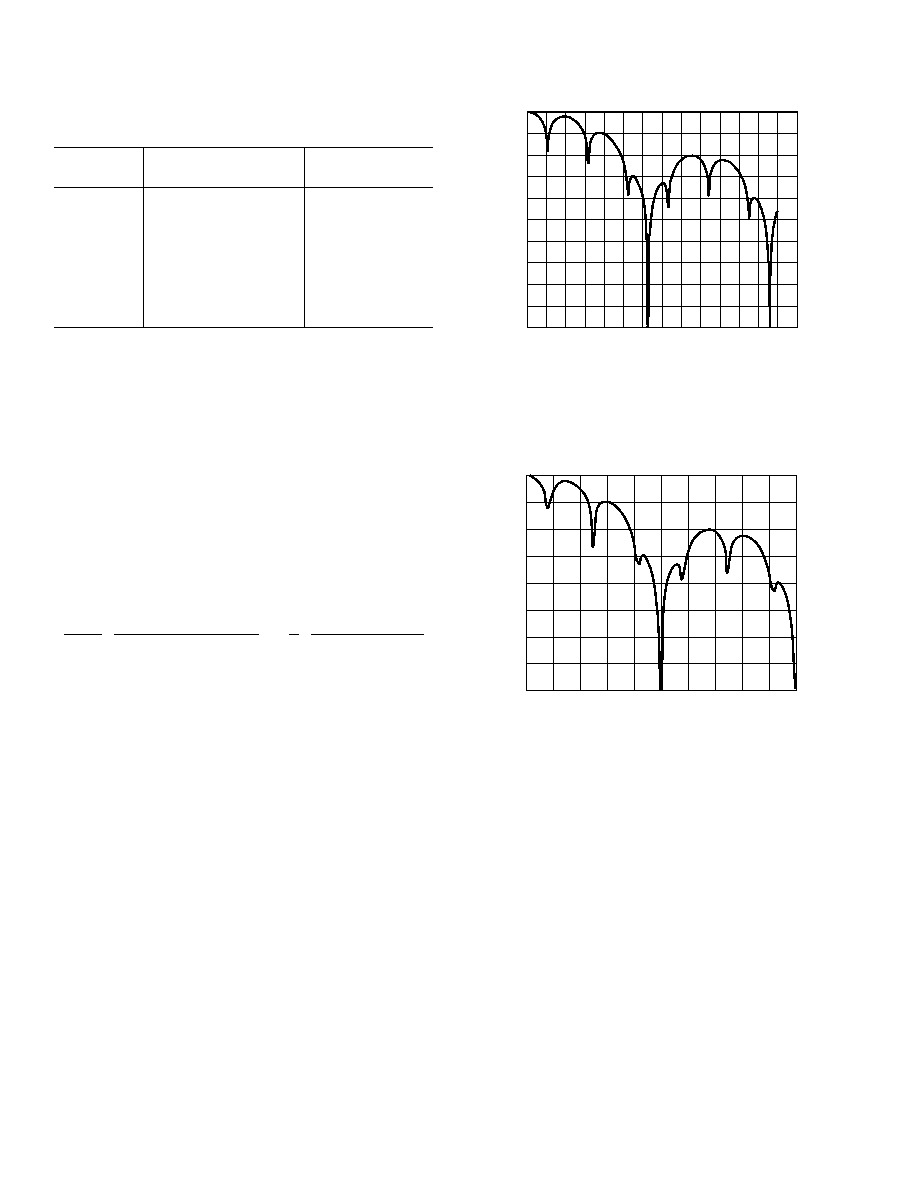
and 60 Hz. Figures 5 to 9 show the filter rejection for a selection
of SF words.
The frequency response of the filter H (f) is as follows:
1
8
8
1
2
2
3
SF
SF
f f
f f
f f
f f
MOD
MOD
OUT
OUT
×
×
× × ×
×
×
×
× ×
×
sin (
/
)
sin (
/
)
sin (
/
)
sin (
/
)
where
f
MOD
= 32,768 Hz,
SF = value programmed into SF Register,
f
OUT
= f
MOD
/(SF
× 8 × 3).
The following plots show the filter frequency response for a
variety of update rates from 5 Hz to 105 Hz.
FREQUENCY Hz
0
140
200
0
650
50 100 150 200 250 300 350 400 450 500 550 600
700
A
TTENUA
TION
dB
20
120
160
180
60
100
40
80
SF = 13
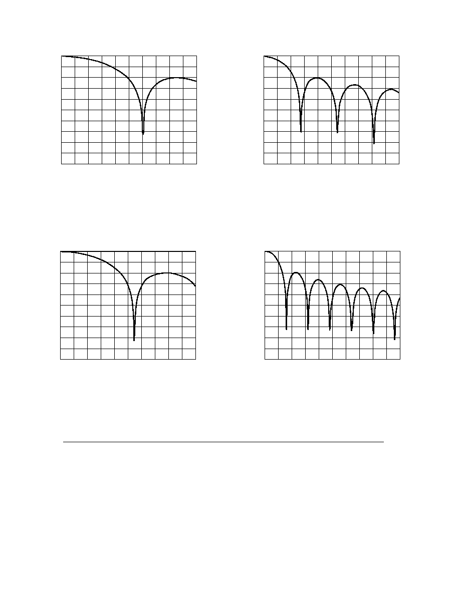
OUTPUT DATA RATE = 105Hz
INPUT BANDWIDTH = 25.2Hz
FIRST NOTCH = 52.5Hz
50Hz REJECTION = 23.6dB, 50Hz 1Hz REJECTION = 20.5dB
60Hz REJECTION = 14.6dB, 60Hz 1Hz REJECTION = 13.6dB
Figure 5. Filter Profile with SF = 13
FREQUENCY Hz
0
80
160
0
100
10
A
TTENUA
TION
dB
20
30
40
50
60
70
80
90
20
40
120
140
60
100
SF = 82
OUTPUT DATA RATE = 16.65Hz
INPUT BANDWIDTH = 4Hz
50Hz REJECTION = 171dB, 50Hz 1Hz REJECTION = 100dB
60Hz REJECTION = 58dB, 60Hz 1Hz REJECTION = 53dB
Figure 6. Filter Profile with SF = 82
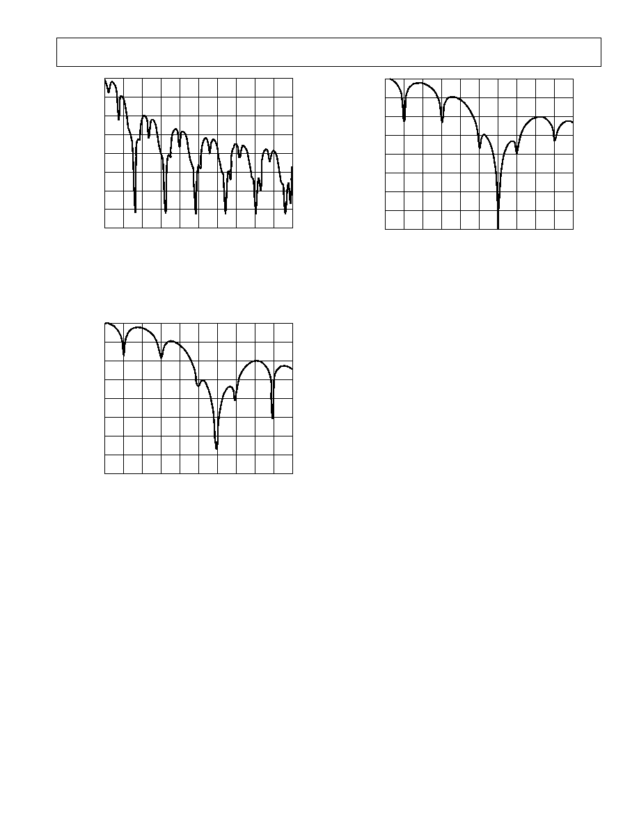
REV. 0
AD7708/AD7718
17
FREQUENCY Hz
0
80
160
0
100
10
A
TTENUA
TION
dB
20
30
40
50
60
70
80
90
20
40
120
140
60
100
SF = 255
OUTPUT DATA RATE = 5.35Hz
INPUT BANDWIDTH = 1.28Hz
50Hz REJECTION = 93dB, 50Hz 1Hz REJECTION = 93dB
60Hz REJECTION = 74dB, 60Hz 1Hz REJECTION = 68dB
Figure 7. Filter Profile with SF = 255
FREQUENCY Hz
0
80
160
0
100
10
A
TTENUA
TION
dB
20
30
40
50
60
70
80
90
20
40
120
140
60
100
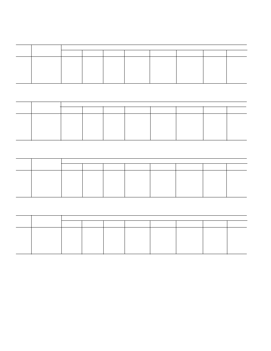
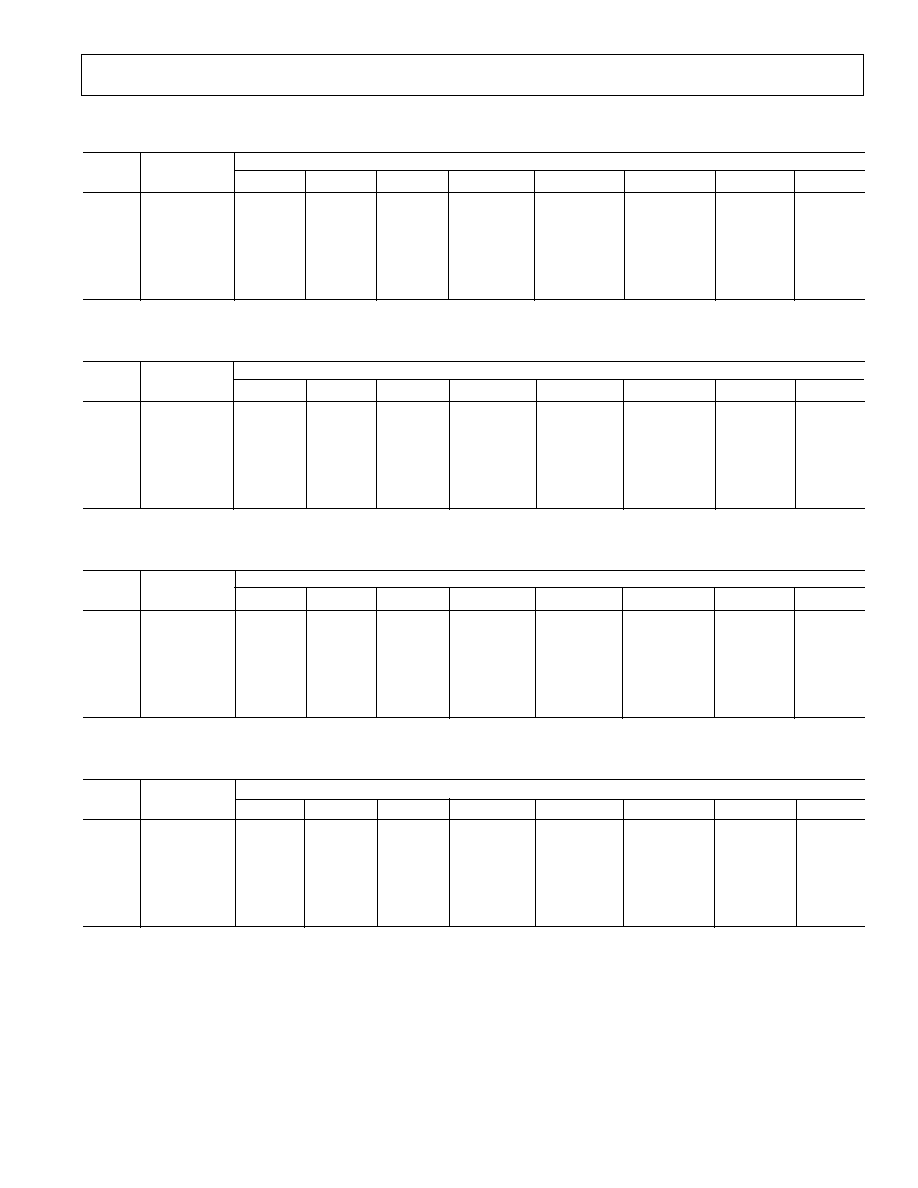
SF = 69
OUTPUT DATA RATE = 19.8Hz
INPUT BANDWIDTH = 4.74Hz
FIRST NOTCH = 9.9Hz
50Hz REJECTION = 66dB, 50Hz 1Hz REJECTION = 60dB
60Hz REJECTION = 117dB, 60Hz 1Hz REJECTION = 94dB
Figure 8. Filter Profile with Default SF = 69 Giving Filter
Notches at Both 50 Hz and 60 Hz
FREQUENCY Hz
0
80
160
0
100
10
A
TTENUA
TION
dB
20
30
40
50
60
70
80
90
20
40
120
140
60
100
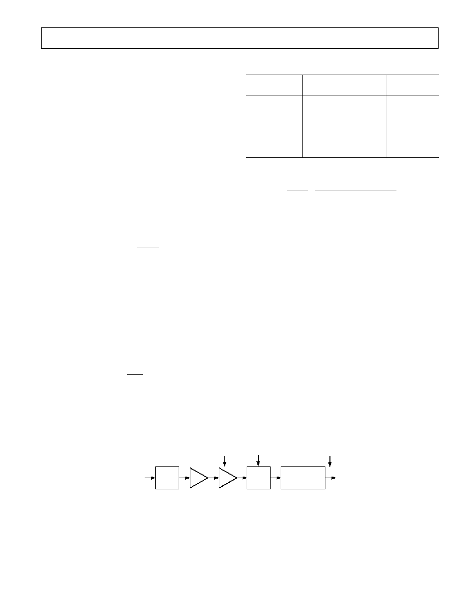
SF = 68
OUTPUT DATA RATE = 20.07Hz
INPUT BANDWIDTH = 4.82Hz
50Hz REJECTION = 74dB, 50Hz 1Hz REJECTION = 54.6dB
60Hz REJECTION = 147dB, 60Hz 1Hz REJECTION = 101dB
Figure 9. Filter Profile with SF = 68
ADC NOISE PERFORMANCE CHOP ENABLED
(
CHOP = 0)
Tables II to V show the output rms noise and output peak-to-
peak resolution in bits (rounded to the nearest 0.5 LSB) for a
selection of output update rates. The numbers are typical and
generated at a differential input voltage of 0 V with AV
DD
=
DV
DD
= 5 V and using a 2.5 V reference. The output update
rate is selected via the SF7SF0 bits in the Filter Register. It is
important to note that the peak-to-peak resolution figures repre-
sent the resolution for which there will be no code flicker within
a six-sigma limit. The output noise comes from two sources. The
first is the electrical noise in the semiconductor devices (device
noise) used in the implementation of the modulator. Secondly,
when the analog input is converted into the digital domain,
quantization noise is added. The device noise is at a low level
and is independent of frequency. The quantization noise starts at
an even lower level but rises rapidly with increasing frequency to
become the dominant noise source. The numbers in the tables
are given for the bipolar input ranges. For the unipolar ranges
the rms noise numbers will be the same as the bipolar range, but
the peak-to-peak resolution is now based on half the signal range
which effectively means losing one bit of resolution.
REV. 0
18
AD7708/AD7718
Table II. Typical Output RMS Noise vs. Input Range and Update Rate for AD7718 with Chop Enabled (
CHOP = 0);
Output RMS Noise in V
SF
Data Update
Input Range
Word
Rate (Hz)
20 mV
40 mV
80 mV
160 mV
320 mV
640 mV
1.28 V
2.56 V
13
105.3
1.50
1.50
1.60
1.75
3.50
4.50
6.70
11.75
23
59.36
1.0
1.02
1.06
1.15
1.22
1.77
3.0
5.08
27
50.56
0.95
0.95
0.98
1.00
1.10
1.66
5.0
69
19.79
0.60
0.65
0.65
0.65
0.65
0.95
1.40
2.30
255
5.35
0.35
0.35
0.37
0.37
0.37
0.51
0.82
1.25
Table III. Peak-to-Peak Resolution vs. Input Range and Update Rate for AD7718 with Chop Enabled (
CHOP = 0);
Peak-to-Peak Resolution in Bits
SF
Data Update
Input Range
Word
Rate (Hz)
20 mV
40 mV
80 mV
160 mV
320 mV
640 mV
1.28 V
2.56 V
13
105.3
12
13
14
15
15
15.5
16
16
23
59.36
12.5
13.5
14.5
15
16
17
17
17
27
50.56
12.5
13.5
14.5
15.5
16.5
17
17
17
69
19.79
13
14
15
16
17
17.5
18
18.5
255
5.35
14
15
16
17
18
18.5
18.8
19.2
Table IV. Typical Output RMS Noise vs. Input Range and Update Rate for AD7708 with Chop Enabled (
CHOP = 0);
Output RMS Noise in V
SF
Data Update
Input Range
Word
Rate (Hz)
20 mV
40 mV
80 mV
160 mV
320 mV
640 mV
1.28 V
2.56 V
13
105.3
1.50
1.50
1.60
1.75
3.50
4.50
6.70
11.75
23
59.36
1.0
1.02
1.06
1.15
1.22
1.77
3.0
5.08
27
50.56
0.95
0.95
0.98
1.00
1.10
1.66
5.0
69
19.79
0.60
0.65
0.65
0.65
0.65
0.95
1.40
2.30
255
5.35
0.35
0.35
0.37
0.37
0.37
0.51
0.82
1.25
Table V. Peak-to-Peak Resolution vs. Input Range and Update Rate for AD7708 with Chop Enabled (
CHOP = 0);
Peak-to-Peak Resolution in Bits
SF
Data Update
Input Range
Word
Rate (Hz)
20 mV
40 mV
80 mV
160 mV
320 mV
640 mV
1.28 V
2.56 V
13
105.3
12
13
14
15
15
15.5
16
16
23
59.35
12.5
13.5
14.5
15
16
16
16
16
27
50.56
12.5
13.5
14.5
15.5
16
16
16
16
69
19.79
13
14
15
16
16
16
16
16
255
5.35
14
15
16
16
16
16
16
16
REV. 0
AD7708/AD7718
19
SIGNAL CHAIN OVERVIEW CHOP DISABLED
(
CHOP = 1)
With
CHOP =1 chopping is disabled. With chopping disabled
the available output rates vary from 16.06 Hz (62.26 ms) to
1365.33 Hz (0.73 ms). The range of applicable SF words is from
3 to 255. When switching between channels with chop disabled,
the channel throughput is increased by a factor of two over the
case where chop is enabled. When used in multiplexed applica-
tions operation with chop disabled will offer the best throughput
time when cycling through all channels. The drawback with
chop disabled is that the drift performance is degraded and
calibration is required following a gain change or significant
temperature change. A block diagram of the ADC input
channel with chop disabled is shown in Figure 10. The
signal chain includes a mux, buffer, PGA, sigma-delta modu-
lator, and digital filter. The modulator bit stream is applied to
a Sinc
3
filter. The programming of the Sinc
3
decimation
factor is restricted to an 8-bit register SF, the actual decima-
tion factor is the register value times 8. The decimated output
rate from the Sinc
3
filter (and the ADC conversion rate) will there-
fore be:
f
f
SF
ADC
MOD
=
×
8
where
f
ADC
is the ADC conversion rate,
SF is the decimal equivalent of the word loaded to the filter
register, valid range is from 3 to 255,
f
MOD
is the modulator sampling rate of 32.768 kHz.
The settling time to a step input is governed by the digital filter.
A synchronized step change will require a settling time of three
times the programmed update rate, a channel change can be
treated as a synchronized step change. An unsynchronized step
change will require four outputs to reflect the new analog input
at its output.
t
f
t
SETTLE
ADC
ADC
=
= ×
3
3
The allowable range for SF is 3 to 255 with a default of 69
(45H). The corresponding conversion rates, conversion times,
and settling times are shown in Table VI. Note that the conver-
sion time increases by 0.245 ms for each increment in SF.
Table VI. ADC Conversion and Settling Times for Various
SF Words with
CHOP = 1
SF
Data Update Rate
Settling Time
Word
f
ADC
(Hz)
t
SETTLE
(ms)
03
1365.33
2.20
68
60.2
49.8
69 (Default)
59.36
50.54
75
54.6
54.93
82
49.95
60
151
27.13
110.6
255
16.06
186.76
The frequency response of the digital filter H (f) is as follows:
1
8
8
3
SF
SF
f f
f f
MOD
MOD
×
×
× × ×
×
sin(
/
)
sin(
/
)
where
f
MOD
= 32,768 Hz,
SF = value programmed into SF SFR.
The following shows plots of the filter frequency response using
different SF words for output data rates
of 16 Hz to 1.36 kHz.
There are sinc
3
notches at integer multiples of the update rate.
The 3 dB frequency for all values of SF obeys the following
equation:
f (3 dB) = 0.262
× f
ADC
The following plots show frequency response of the AD7708/
AD7718 digital filter for various filter words. The AD7708/
AD7718 are targeted at multiplexed applications. One of the
key requirements in these applications is to optimize the SF
word to obtain the maximum filter rejection at 50 Hz and 60 Hz
while minimizing the channel throughput rate. Figure 12 shows
the AD7708/AD7718 optimized throughput while maximizing
50 Hz and 60 Hz rejection. This is achieved with an SF word of
75. In Figure 13, by using a higher SF word of 151, 50 Hz and
60 Hz rejection can be maximized at 60 dB with a channel
throughput rate of 110 ms. An SF word of 255 gives maximum
rejection at both 50 Hz and 60 Hz but the channel throughput
rate is restricted to 186 ms as shown in Figure 14.
SINC
3
FILTER
MUX
BUF
PGA
-
MOD0
ANALOG
INPUT
DIGITAL
OUTPUT
f
IN
f
MOD
f
ADC
Figure 10. ADC Channel Block Diagram with CHOP Disabled
REV. 0
20
AD7708/AD7718
FREQUENCY Hz
0
80
160
0
100
10
A
TTENUA
TION
dB
20
30
40
50
60
70
80
90
20
40
120
140
60
100
SF = 68
OUTPUT DATA RATE = 60.2Hz
SETTLING TIME = 49.8ms
INPUT BANDWIDTH = 15.5Hz
50Hz REJECTION = 43dB, 50Hz 1Hz REJECTION = 40dB
60Hz REJECTION = 147dB, 60Hz 1Hz REJECTION = 101dB
200
180
Figure 11. Frequency Response Operating with the
SF Word of 68
FREQUENCY Hz
0
80
160
0
100
10
A
TTENUA
TION
dB
20
30
40
50
60
70
80
90
20
40
120
140
60
100
SF = 75
OUTPUT DATA RATE = 54.6Hz
SETTLING TIME = 55ms
INPUT BANDWIDTH = 14.3Hz
50Hz REJECTION = 62.5dB, 50Hz 1Hz REJECTION = 57dB
60Hz REJECTION = 63dB, 60Hz 1Hz REJECTION = 60dB
200
180
Figure 12. Optimizing Filter Response for Throughput
while Maximizing the Simultaneous 50 Hz and 60 Hz
Rejection
FREQUENCY Hz
0
80
160
0
100
10
A
TTENUA
TION
dB
20
30
40
50
60
70
80
90
20
40
120
140
60
100
SF = 151
OUTPUT DATA RATE = 27.12Hz
SETTLING TIME = 110ms
INPUT BANDWIDTH = 27.12Hz
50Hz REJECTION = 65.4dB, 50Hz 1Hz REJECTION = 60dB
60Hz REJECTION = 63dB, 60Hz 1Hz REJECTION = 60dB
200
180
Figure 13. Optimizing Filter Response for Maximum
Simultaneous 50 Hz and 60 Hz Rejection
FREQUENCY Hz
0
80
160
0
100
10
A
TTENUA
TION
dB
20
30
40
50
60
70
80
90
20
40
120
140
60
100
SF = 255
OUTPUT DATA RATE = 16.06Hz
SETTLING TIME = 186ms
INPUT BANDWIDTH = 4.21Hz
50Hz REJECTION = 87dB, 50Hz 1Hz REJECTION = 77dB
60Hz REJECTION = 72dB, 60Hz 1Hz REJECTION = 68dB
200
180
Figure 14. Frequency with Maximum SF Word = 255
ADC NOISE PERFORMANCE CHOP DISABLED
(
CHOP = 1)
Tables VII to X show the output rms noise and output peak-to-
peak resolution in bits (rounded to the nearest 0.5 LSB) for
some typical output update rates. The numbers are typical and
generated at a differential input voltage of 0 V. The output update
rate is selected via the SF7SF0 bits in the Filter Register. It is
important to note that the peak-to-peak resolution figures represent
the resolution for which there will be no code flicker within a
six-sigma limit. The output noise comes from two sources. The
first is the electrical noise in the semiconductor devices (device
noise) used in the implementation of the modulator. Secondly,
when the analog input is converted into the digital domain,
quantization noise is added. The device noise is at a low level
and is independent of frequency. The quantization noise starts
at an even lower level but rises rapidly with increasing frequency
to become the dominant noise source. The numbers in the
tables are given for the bipolar input ranges. For the unipolar
ranges the rms noise numbers will be the same as the bipolar
range, but the peak-to-peak resolution is now based on half the
signal range which effectively means losing 1 bit of resolution.
REV. 0
AD7708/AD7718
21
Table VII. Typical Output RMS Noise vs. Input Range and Update Rate for AD7718 with Chop Disabled (
CHOP = 1);
Output RMS Noise in V
SF
Data Update
Input Range
Word
Rate (Hz)
20 mV
40 mV
80 mV
160 mV
320 mV
640 mV
1.28 V
2.56 V
03
1365.33
30.31
29.02
58.33
112.7
282.44
361.72
616.89
1660
13
315.08
2.47
2.49
2.37
3.87
7.18
12.61
16.65
32.45
66
62.06
0.743
0.852
0.9183
0.8788
0.8795
1.29
1.99
3.59
69
59.38
0.961
0.971
0.949
0.922
0.923
1.32
2.03
3.73
81
50.57
0.894
0.872
0.872
0.806
0.793
1.34
2.18
2.96
255
16.06
0.475
0.468
0.434
0.485
0.458
0.688
1.18
1.78
Table VIII. Peak-to-Peak Resolution vs. Input Range and Update Rate for AD7718 with Chop Disabled (
CHOP = 1);
Peak-to-Peak Resolution in Bits
SF
Data Update
Input Range
Word
Rate (Hz)
20 mV
40 mV
80 mV
160 mV
320 mV
640 mV
1.28 V
2.56 V
03
1365.33
8
9
9
9
9
9
9
9
13
315.08
11
12
14
14
14
14
15
15
66
62.06
13
14
15
16
17
17
18
18
69
59.36
13
14
15
16
17
17
18
18
81
50.57
13
14
15
16
17
17
18
18
255
16.06
14
15
16
17
18
18
19
19
Table IX. Typical Output RMS Noise vs. Input Range and Update Rate for AD7708 with Chop Disabled (
CHOP = 1);
Output RMS Noise in V
SF
Data Update
Input Range
Word
Rate (Hz)
20 mV
40 mV
80 mV
160 mV
320 mV
640 mV
1.28 V
2.56 V
03
1365.33
30.31
29.02
58.33
112.7
282.44
361.72
616.89
1660
13
315.08
2.47
2.49
2.37
3.87
7.18
12.61
16.65
32.45
66
62.06
0.743
0.852
0.9183
0.8788
0.8795
1.29
1.99
3.59
69
59.38
0.961
0.971
0.949
0.922
0.923
1.32
2.03
3.73
81
50.57
0.894
0.872
0.872
0.806
0.793
1.34
2.18
2.96
255
16.06
0.475
0.468
0.434
0.485
0.458
0.688
1.18
1.78
Table X. Peak-to-Peak Resolution vs. Input Range and Update Rate for AD7708 with Chop Disabled (
CHOP = 1);
Peak-to-Peak Resolution in Bits
SF
Data Update
Input Range
Word
Rate (Hz)
20 mV
40 mV
80 mV
160 mV
320 mV
640 mV
1.28 V
2.56 V
03
1365.33
8
9
9
9
9
9
9
9
13
315.08
11
12
14
14
14
14
15
15
66
62.06
13
14
15
16
16
16
16
16
69
59.36
13
14
15
16
16
16
16
16
81
50.57
13
14
15
16
16
16
16
16
255
16.06
14
15
16
16
16
16
16
16
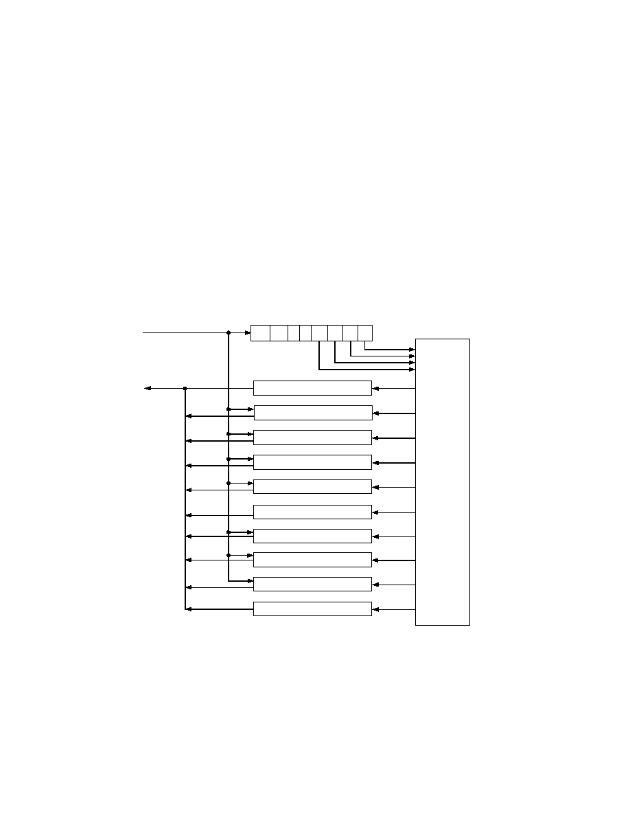
REV. 0
22
AD7708/AD7718
ON-CHIP REGISTERS
The AD7708 and AD7718 are controlled and configured via
a number of on-chip registers which are shown in Figure 15.
The first of these registers is the communications register
which is used to control all operations on these converters. All
communications with these parts must start with a write to
the communications register to specify the next operation to
be performed. After a power-on or RESET, the device defaults
to waiting for a write to the communications register. The
STATUS register contains information pertaining to the operat-
ing conditions of the converter. The STATUS register is a read
only register. The MODE register is used to configure the con-
version mode, calibration, chop enable/disable, reference select,
channel configuration and buffered or unbuffered operation on
the AINCOM analog input. The MODE register is a read/write
register. The ADC Control register is a read/write register used
to select the active channel and program its input range and
bipolar/unipolar operation. The I/O control register is a read/
write register used to configure the operation of the 2-pin I/O
port. The filter register is a read/write register used to program
the data update rate of the converter. The ADC Data register is
a read only register that contains the result of a data conversion
on the selected channel. The ADC offset registers are read/write
registers that contain the offset calibration data. There are five
offset registers, one for each of the fully differential input channels.
When configured for pseudo-differential input mode the chan-
nels share offset registers. The ADC gain registers are read/write
registers that contain the gain calibration data. There are five
ADC gain registers, one for each of the fully differential input
channels. When configured for pseudo differential input mode
the channels share gain registers. The ADC contains Test registers
for factory use only, the user is advised not to alter the oper-
ating conditions of these registers. The ID register is a read only
register and is used for silicon identification purposes. The follow-
ing sections contains more in-depth detail on all of these registers.
In the following descriptions, SET implies a Logic 1 state and
CLEARED implies a Logic 0 state unless otherwise stated.
DOUT
DOUT
DOUT
DIN
DOUT
DIN
DOUT
DIN
DOUT
DIN
DOUT
DOUT
DIN
DOUT
DOUT
WEN R/W
0
0
A1
A2
A3
A0
COMMUNICATIONS REGISTER
DOUT
DIN
DIN
REGISTER
SELECT
DECODER
ADC DATA REGISTER
STATUS REGISTER
MODE REGISTER
ADC CONTROL REGISTER
I/O CONTROL REGISTER
FILTER REGISTER
ID REGISTER
TEST REGISTER
ADC GAIN REGISTER
ADC OFFSET REGISTER
DIN
DIN
Figure 15. On-Chip Registers
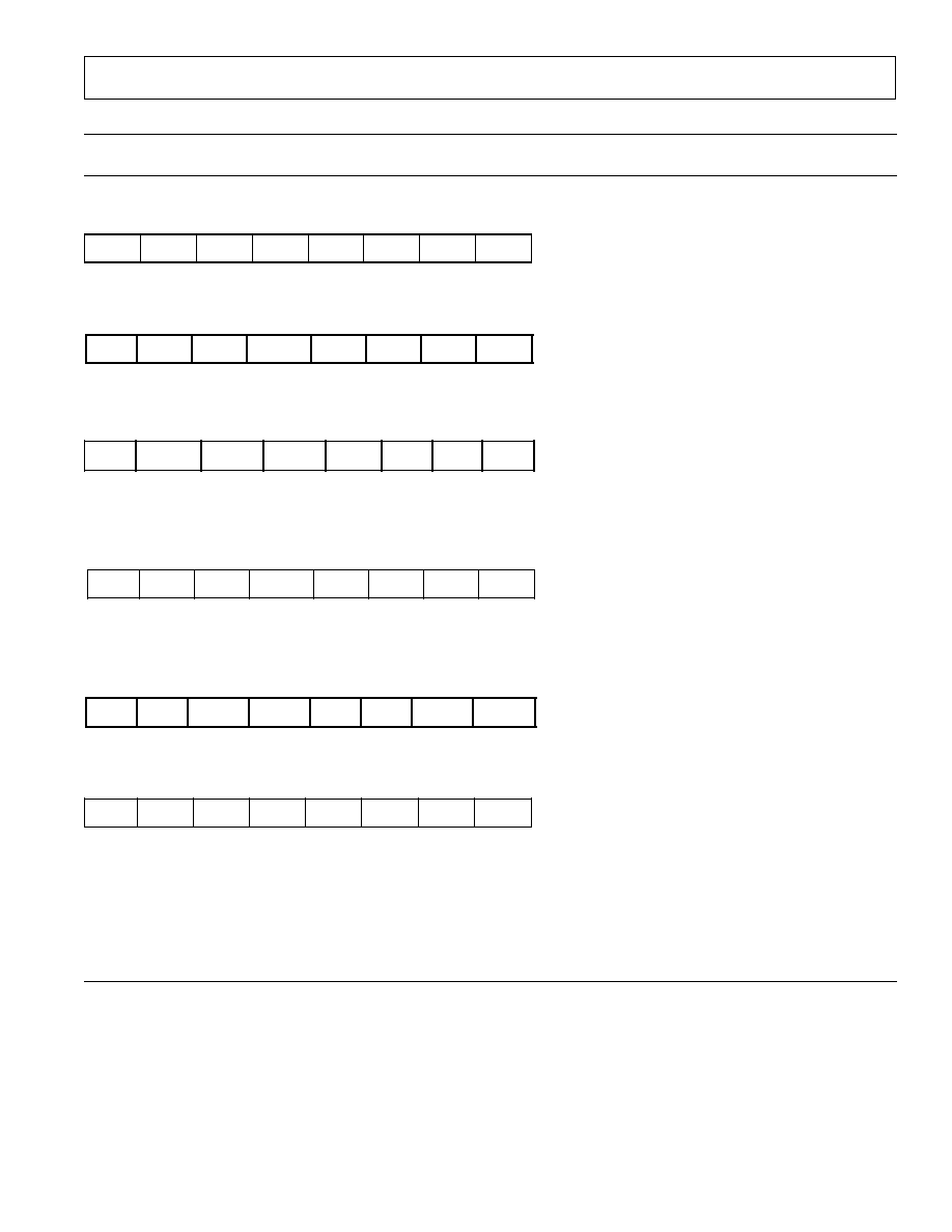
REV. 0
AD7708/AD7718
23
Table XI. Registers--Quick Reference Guide
Power-On/Reset
Register Name
Type
Size
Default Value
Function
Communications
Write Only
8 Bits
Not Applicable
All operations to other registers are initiated through
the Communications Register. This controls whether
subsequent operations are read or write operations
and also selects the register for that subsequent
operation.
Status Register
Read Only
8 Bits
00 Hex
Provides status information on conversions, calibra-
tions and error conditions.
Mode Register
Read/Write
8 Bits
00 Hex
Controls functions such as mode of operation, chan-
nel configuration, oscillator operation in power-down.
ADC (ADCCON)
Control Register
Read/Write
8 Bits
07 Hex
This register is used to select the active channel
input, configure the operating input range, and select
unipolar or bipolar operation.
I/O (IOCON)
I/O Control Register
Read/Write
8 Bits
00 Hex
This register is used to control and configure the
I/O port.
Filter Register
Read/Write
8 Bits
45 Hex
This register determines the amount of averaging
performed by the sinc filter and consequently deter-
mines the data update rate of the AD7708/AD7718.
The filter register determines the update rate for
operation with CHOP enabled and CHOP disabled.
AD7718 ADC (DATA)
Data Register
Read Only
24 Bits
000000 Hex
Provides the most up-to-date conversion result for
the selected channel on the AD7718.
AD7708 (DATA)
Data Register
Read Only
16 Bits
0000 Hex
Provides the most up-to-date conversion result for
the selected channel on the AD7708.
B
S
M
B
S
L
Y
D
R
0
L
A
C
0
R
R
E
0
0
K
C
O
L
B
S
M
B
S
L
3
H
C
2
H
C
1
H
C
0
H
C
/
U
B
2
N
R
1
N
R
0
N
R
B
S
M
B
S
L
7
F
S
6
F
S
5
F
S
4
F
S
3
F
S
2
F
S
1
F
S
0
F
S
B
S
M
B
S
L
0
0
R
I
D
2
P
R
I
D
1
P
0
0
T
A
D
2
P
T
A
D
1
P
CR7
CR6
CR5
CR4
CR3
CR2
CR1
CR0
WEN
R/
W
0(0)
0(0)
A3(0)
A2(0)
A1(0)
A0(0)
MSB
LSB
CHOP NEGBUF REFSEL CHCON OSCPD
MD2
MD1
MD0

REV. 0
24
AD7708/AD7718
Table XI. Registers--Quick Reference Guide (continued)
Power-On/Reset
Register Name
Type
Size
Default Value
Function
AD7718
Offset Register
Read/Write
24 Bits
800 000 Hex
Contains a 24-bit word which is the offset calibration
coefficient for the part. The contents of this register
are used to provide offset correction on the output
from the digital filter. There are five Offset Registers
on the part and these are associated with input chan-
nels as outlined in the ADCCON register.
AD7718
Gain Register
Read/Write
24 Bits
5XXXX5 Hex
Contains a 24-bit word which is the gain calibration
coefficient for the part. The contents of this register
are used to provide gain correction on the output
from the digital filter. There are five Gain Registers
on the part and these are associated with input chan-
nels as outlined in the ADCCON register.
AD7708
Offset Register
Read/Write
16 Bits
8000 Hex
Contains a 16-bit word which is the offset calibration
coefficient for the part. The contents of this register
are used to provide offset correction on the output
from the digital filter. There are five Offset Registers
on the part and these are associated with input chan-
nels as outlined in the ADCCON register.
AD7708
Gain Register
Read/Write
16 Bits
5XXX Hex
Contains a 16-bit word which is the gain calibration
coefficient for the part. The contents of this register
are used to provide gain correction on the output
from the digital filter. There are five Gain Registers
on the part and these are associated with input chan-
nels as outlined in the ADCCON register.
AD7708
ID Register
Read
8 Bits
5X Hex
Contains an 8-bit byte which is the identifier for
the part.
AD7718
ID Register
Read
8 Bits
4X Hex
Contains an 8-bit byte which is the identifier for
the part.
Test Registers
Read/Write
16 Bits
0000 Hex
Controls the test modes of the part that are used
when testing the part. The user is advised not to
change the contents of these registers.
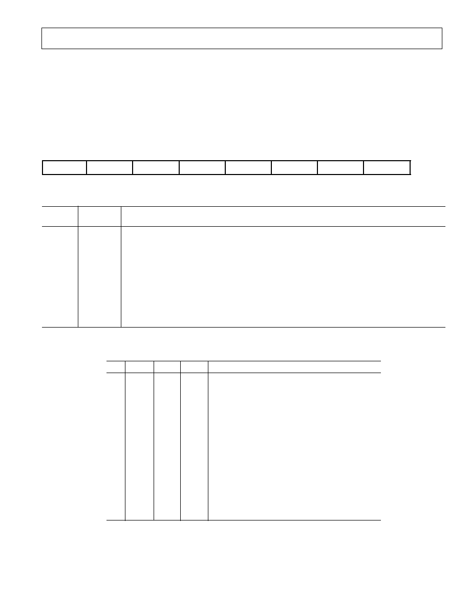
REV. 0
AD7708/AD7718
25
Communications Register (A3, A2, A1, A0 = 0, 0, 0, 0)
The Communications Register is an 8-bit write-only register. All communications to the part must start with a write operation to the
Communications Register. The data written to the Communications Register determines whether the next operation is a read or write
operation, the type of read operation, and on which register this operation takes place. For read or write operations, once the subse-
quent read or write operation to the selected register is complete, the interface returns to where it expects a write operation to the
Communications Register. This is the default state of the interface and, on power-up or after a
RESET, the AD7708/AD7718 is in
this default state waiting for a write operation to the Communications Register. In situations where the interface sequence is lost, a
write operation of at least 32 serial clock cycles with DIN high returns the AD7708/AD7718 to this default state by resetting the part.
Table XII outlines the bit designations for the Communications Register. CR0 through CR7 indicate the bit location, CR denoting
the bits are in the Communications Register. CR7 denotes the first bit of the data stream.
7
R
C
6
R
C
5
R
C
4
R
C
3
R
C
2
R
C
1
R
C
0
R
C
N
E
W
)
0
(
/
R
W
)
0
(
)
0
(
0
)
0
(
0
)
0
(
3
A
)
0
(
2
A
)
0
(
1
A
)
0
(
0
A
Table XII. Communications Register Bit Designations
Bit
Bit
Location
Mnemonic
Description
CR7
WEN
Write Enable Bit. A 0 must be written to this bit so the write operation to the Communications Register
actually takes place. If a 1 is written to this bit, the part will not clock on to subsequent bits in the regis
ter. It will stay at this bit location until a 0 is written to this bit. Once a 0 is written to the
WEN bit, the
next seven bits will be loaded to the Communications Register.
CR6
R/
W
A zero in this bit location indicates that the next operation will be a write to a specified register. A one in
this position indicates that the next operation will be a read from the designated register.
CR5
0
A zero must be written to this bit position to ensure correct operation of the AD7708/AD7718.
CR4
0
A zero must be written to this bit position to ensure correct operation of the AD7708/AD7718.
CR3CR0
A3A0
Register Address Bits. These address bits are used to select which of the AD7708/AD7718's registers are
being accessed during this serial interface communication. A3 is the MSB of the three selection bits.
Table XIII. Register Selection Table
A3
A2
A1
A0
Register
0
0
0
0
Communications Register during a Write Operation
0
0
0
0
Status Register during a Read Operation
0
0
0
1
Mode Register
0
0
1
0
ADC Control Register
0
0
1
1
Filter Register
0
1
0
0
ADC Data Register
0
1
0
1
ADC Offset Register
0
1
1
0
ADC Gain Register
0
1
1
1
I/O Control Register
1
0
0
0
Undefined
1
0
0
1
Undefined
1
0
1
0
Undefined
1
0
1
1
Undefined
1
1
0
0
Test 1 Register
1
1
0
1
Test 2 Register
1
1
1
0
Undefined
1
1
1
1
ID Register
REV. 0
26
AD7708/AD7718
Status Register (A3, A2, A1, A0 = 0, 0, 0, 0; Power-On-Reset = 00Hex)
The ADC Status Register is an 8-bit read-only register. To access the ADC Status Register, the user must write to the Communica-
tions Register selecting the next operation to be a read and load Bits A3-A0 with 0, 0, 0,0. Table XIV outlines the bit designations
for the Status Register. SR0 through SR7 indicate the bit location, SR denoting the bits are in the Status Register. SR7 denotes the
first bit of the data stream. The number in brackets indicates the power-on/reset default status of that bit.
R
S 7
6
R
S
5
R
S
4
R
S
3
R
S
2
R
S
1
R
S
0
R
S
Y
D
R
)
0
(
)
0
(
0
)
0
(
L
A
C
)
0
(
0
)
0
(
R
R
E
)
0
(
0
)
0
(
0
)
0
(
K
C
O
L
Table XIV. Status Register Bit Designations
Bit
Bit
Location
Mnemonic Description
SR7
RDY
Ready Bit for the ADC
Set when data is transferred to the ADC data registers or on completion of calibration cycle. The RDY
bit is cleared automatically a period of time before the data register is updated with a new conversion
result or after the ADC data register has been read. This bit is also cleared by a write to the mode bits to
indicate a conversion or calibration. The
RDY pin is the complement of the RDY bit.
SR6
0
Bit is automatically cleared. Reserved for future use
SR5
CAL
Calibration Status Bit
Set to indicate completion of calibration. It is set at the same time that the RDY is set high.
Cleared by a write to the mode bits to start another ADC conversion or calibration.
SR4
0
This bit is automatically cleared. Reserved for future use
SR3
ERR
ADC Error Bit
Set to indicate that the result written to the ADC data register has been clamped to all zeros or all ones.
After a calibration this bit also flags error conditions that caused the calibration registers not to be
written. Error sources include Overrange.
Cleared by a write to the mode bits to initiate a conversion or calibration.
SR2
0
This bit is automatically cleared. Reserved for future use
SR1
0
This bit is automatically cleared. Reserved for future use
SR0
LOCK
PLL Lock Status Bit.
Set if the PLL has locked onto the 32.768 kHz crystal oscillator clock. If the user is worried about
exact sampling frequencies etc., the LOCK bit should be interrogated and the result discarded if the
LOCK bit is zero.
REV. 0
AD7708/AD7718
27
Mode Register (A3, A2, A1, A0 = 0, 0, 0, 1; Power-On-Reset = 00Hex)
The Mode Register is an 8-bit register from which data can be read or to which data can be written. This register configures the
operating modes of the AD7708/AD7718. Table XV outlines the bit designations for the Mode Register. MR7 through MR0 indi-
cate the bit location, MR denoting the bits are in the Mode Register. MR7 denotes the first bit of the data stream. The number in
brackets indicates the power-on/reset default status of that bit.
7
R
M
6
R
M
5
R
M
4
R
M
3
R
M
2
R
M
1
R
M
0
R
M
P
O
H
C
)
0
(
)
0
(
F
U
B
G
E
N
)
0
(
L
E
S
F
E
R
)
0
(
N
O
C
H
C
)
0
(
D
P
C
S
O
)
0
(
2
D
M
)
0
(
1
D
M
)
0
(
0
D
M
Table XV. Mode Register Bit Designations
Bit
Bit
Location
Mnemonic
Description
MR7
CHOP
If this bit is cleared, chopping is enabled. When this bit is set chopping is disabled. The default is for
chop enabled.
MR6
NEGBUF
This bit controls the operation of the input buffer on the AINCOM input when a channel is config-
ured for pseudo-differential mode of operation. If cleared, the analog negative input (AINCOM) is
unbuffered allowing it to be tied to AGND in single-ended input configuration. If this bit is set the
analog negative input (AINCOM) is buffered, placing a restriction on its common-mode input range.
MR5
REFSEL
If this bit is cleared, the reference selected is REFIN1(+) and REFIN1() for the active channel. If
this bit is set, the reference selected is REFIN2(+) and REFIN2() for the active channel. The con-
tents of the CHCON bit overrides the REFSEL bit. If the ADC is configured in five fully-differential
or 10 pseudo-differential input channel mode, the REFSEL bit setting is irrelevant as only one
reference input is available. V
REF
Select implemented using the REFSEL bit enables the user to
perform both absolute and ratiometric measurements.
MR4
CHCON
When cleared the device is configured as an 8-input channel converter, configured as eight pseudo-
differential input channels with respect to AINCOM or four differential input arrangements
with two reference input selection options. When set the device is configured as a 10 pseudo-
differential input or a five differential input channel arrangement with a single reference
input option.
MR3
OSCPD
Oscillator Power-Down Bit.
If this bit is set, placing the AD7708/AD7718 in standby mode will stop the crystal oscillator reducing
the power drawn by these parts to a minimum. The oscillator will require 300 ms to begin oscillating
when the ADC is taken out of standby mode. If this bit is cleared, the oscillator is not shut off when
the ADC is put into standby mode and will not require the 300 ms start-up time when the ADC is
taken out of standby.
MR2MR0
MD2MD0
ADC Mode Bits.
These bits select the operational mode of the ADC as follows:
MD2
MD1
MD0
0
0
0
Power-Down Mode (Power-On Default)
0
0
1
Idle Mode
In Idle Mode the ADC filter and modulator are held in a reset state although the modulator clocks
are still provided.
0
1
0
Single Conversion Mode
In Single Conversion Mode, a single conversion is performed on the enabled channels. On comple-
tion of the conversion the ADC data registers are updated, the relevant flags in the STATUS register
are written, and idle mode is reentered with the MD2MD0 being written accordingly to 001.
0
1
1
Continuous Conversion
In continuous conversion mode, the ADC data registers are regularly updated at the selected update
rate (see Filter register).
1
0
0
Internal Zero-Scale Calibration
Internal short automatically connected to the enabled channel(s)
1
0
1
Internal Full-Scale Calibration
External V
REF
is connected automatically to the ADC input for this calibration.
1
1
0
System Zero-Scale Calibration
User should connect system zero-scale input to the channel input pins as selected by CH3CH0 bits
in the control registers.
1
1
1
System Full-Scale Calibration
User should connect system full-scale input to the channel input pins as selected by CH3CH0 bits
in the control registers.
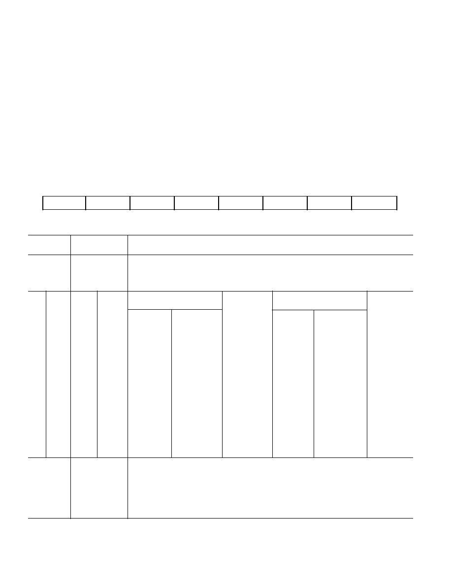
REV. 0
28
AD7708/AD7718
Operating Characteristics when Addressing the Mode and Control Registers
1. Any change to the MD bits will immediately reset the ADCs. A write to the MD2MD0 bits with no change is also treated as a reset.
2. Once the MODE has been written with a calibration mode, the RDY bit (STATUS) is immediately reset and the calibration
commences. On completion the appropriate calibration registers are written, the bit in STATUS register is updated and the
MD2MD0 bits are reset to 001 to indicate the ADC is back in idle mode.
3. Calibrations are performed with the maximum allowable SF value with chop enabled. SF register is reset to user configuration
after calibration with chop enabled. Calibrations are performed with the selected value of SF when chop is disabled.
ADC Control Register (ADCCON): (A3, A2, A1, A0 = 0, 0, 1, 0; Power-On-Reset = 07 Hex)
The ADC Control Register is an 8-bit register from which data can be read or to which data can be written. This register is used to
configure the ADC for range, channel selection, and unipolar or bipolar coding. Table XVI outlines the bit designations for the ADC
control register ADCCON7 through ADCCON0 indicate the bit location, ADCCON denoting the bits are in the ADC Control
Register. ADCCON7 denotes the first bit of the data stream. The number in brackets indicates the power-on/reset default status of
that bit.
Table XVI. ADC Control Register (ADCCON) Bit Designations
Bit
Bit
Location
Mnemonic
Description
ADCCON7
CH3
ADC Channel Selection Bits. Written by the user to select either pseudo-differential or fully-
ADCCON6
CH2
differential input pairs used by the ADC as follows:
ADCCON5
CH1
ADCCON4
CH0
8-Channel Configuration
10-Channel Configuration
(CHCON = 0)
(CHCON = 1)
Positive
Negative
Cal Register
Positive
Negative
Cal Register
CH3
CH2
CH1
CH0
Input
Input
Pair
Input
Input
Pair
0
0
0
0
AIN1
AINCOM
1
AIN1
AINCOM
1
0
0
0
1
AIN2
AINCOM
2
AIN2
AINCOM
2
0
0
1
0
AIN3
AINCOM
3
AIN3
AINCOM
3
0
0
1
1
AIN4
AINCOM
4
AIN4
AINCOM
4
0
1
0
0
AIN5
AINCOM
1
AIN5
AINCOM
5
0
1
0
1
AIN6
AINCOM
2
AIN6
AINCOM
1
0
1
1
0
AIN7
AINCOM
3
AIN7
AINCOM
2
0
1
1
1
AIN8
AINCOM
4
AIN8
AINCOM
3
1
0
0
0
AIN1
AIN2
1
AIN1
AIN2
1
1
0
0
1
AIN3
AIN4
2
AIN3
AIN4
2
1
0
1
0
AIN5
AIN6
3
AIN5
AIN6
3
1
0
1
1
AIN7
AIN8
4
AIN7
AIN8
4
1
1
0
0
AIN2
AIN2
1
AIN9
AIN10
5
1
1
0
1
AINCOM
AINCOM
1
AINCOM
AINCOM
1
1
1
1
0
REFIN(+)
REFIN()
1
AIN9
AINCOM
4
1
1
1
1
OPEN
OPEN
1
AIN10
AINCOM
5
ADCCON3
U/
B
Unipolar/Bipolar Bit.
Set by user to enable unipolar coding i.e., zero differential input will result in 000000hex
output and a full-scale differential input will result in FFFFFF Hex output when operated in
24-bit mode.
Cleared by user to enable bipolar coding, Negative full-scale differential input will result in an
output code of 000000 Hex, zero differential input will result in an output code of 800000 Hex
and a positive full-scale differential input will result in an output code of FFFFFF Hex.
ADCCON7
ADCCON6
ADCCON5
ADCCON4
ADCCON3
ADCCON2
ADCCON1
ADCCON0
CH3 (0)
CH2 (0)
CH1 (0)
CH0 (0)
U/
B (0)
RN2 (1)
RN1 (1)
RN0 (1)
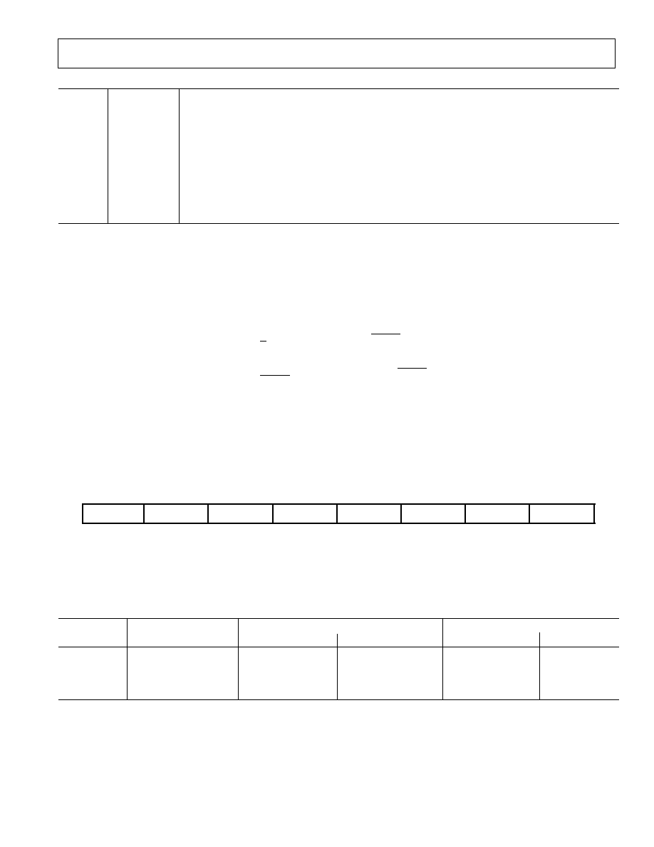
REV. 0
AD7708/AD7718
29
AD0C2
RN2
ADC Range Bits
AD0C1
RN1
Written by the user to select the ADC input range as follows
AD0C0
RN0
RN2
RN1
RN0
Selected ADC Input Range (VREF = 2.5 V)
0
0
0
±20 mV
0
0
1
±40 mV
0
1
0
±80 mV
0
1
1
±160 mV
1
0
0
±320 mV
1
0
1
±640 mV
1
1
0
±1.28 V
1
1
1
±2.56 V
Filter Register (A3, A2, A1, A0 = 0, 0, 1, 1; Power-On Reset = 45Hex)
The Filter Register is an 8-bit register from which data can be read or to which data can be written. This register determines the
amount of averaging performed by the sinc filter. Table XVII outlines the bit designations for the Filter Register. FR7 through FR0
indicate the bit location, FR denoting the bits are in the Filter Register. FR7 denotes the first bit of the data stream. The number in
brackets indicates the power-on/reset default status of that bit. The number in this register is used to set the decimation factor and
thus the output update rate for the ADCs. The filter register cannot be written to by the user the ADC is active. The update rate is
used for the ADCs is calculated as follows:
f
f
CHOP Enabled CHOP
f
SF
f
CHOP Disabled CHOP
ADC
MOD
ADC
MOD
= ×
=
=
×
×
=
(
)
(
)
1
3
0
1
8
1
where
f
ADC
= ADC Output Update Rate,
f
MOD
= Modulator Clock Frequency = 32.768 kHz,
SF
= Decimal Value Written to SF Register.
Table XVII. Filter Register Bit Designations
7
R
F
6
R
F
5
R
F
4
R
F
3
R
F
2
R
F
1
R
F
0
R
F
)
0
(
7
F
S
6
F
S
)
1
(
5
F
S
)
0
(
4
F
S
)
0
(
3
F
S
)
0
(
)
1
(
2
F
S
)
0
(
1
F
S
)
1
(
0
F
S
The allowable range for SF is 13 decimal to 255 decimal with chop enabled, and the allowable SF range when chop is disabled is 03
decimal to 255 decimal. Examples of SF values and corresponding conversion rate (f
ADC
) and time (t
ADC
) are shown in Table XVIII.
It should be noted that optimum performance is obtained when operating with chop enabled. When chopping is enabled (
CHOP = 0),
the filter register is loaded with FF HEX during a calibration cycle. With chop disabled (
CHOP =1), the value in the filter register is
used during calibration.
Table XVIII. Update Rate vs. SF Word
CHOP Enabled
CHOP Disabled
SF (Dec)
SF (Hex)
f
ADC
(Hz)
t
ADC
(ms)
f
ADC
(Hz)
t
ADC
(ms)
03
03
N/A
N/A
1365.33
0.732
13
0D
105.3
9.52
315
3.17
69
45
19.79
50.34
59.36
16.85
255
FF
5.35
186.77
16.06
62.26
Table XVI. ADC Control Register (ADCCON) Bit Designations (continued)
REV. 0
30
AD7708/AD7718
I/O Control Register (IOCON): (A3, A2, A1, A0 = 0, 1, 1, 1; Power-On-Reset = 00Hex)
The IOCON Register is an 8-bit register from which data can be read or to which data can be written. This register is used to con-
trol and configure the I/O port. Table XIX outlines the bit designations for this register. IOCON7 through IOCON0 indicate the
bit location, IOCON denoting the bits are in the I/O Control Register. IOCON7 denotes the first bit of the data stream. The num-
ber in brackets indicates the power-on/reset default status of that bit. A write to the IOCON register has immediate effect and does
not reset the ADCs.
7
N
O
C
O
I
6
N
O
C
O
I
5
N
O
C
O
I
4
N
O
C
O
I
3
N
O
C
O
I
2
N
O
C
O
I
1
N
O
C
O
I
0
N
O
C
O
I
)
0
(
0
)
0
(
)
0
(
R
I
D
2
P
R
I
D
1
P
)
0
(
0
)
0
(
)
0
(
0
)
0
(
T
A
D
2
P
)
0
(
T
A
D
1
P
Table XIX. IOCON (I/O Control Register) Bit Designations
Bit
Bit
Location
Mnemonic
Description
IOCON7
0
This bit should always be cleared. Reserved for future use.
IOCON6
0
This bit should always be cleared. Reserved for future use.
IOCON5
P2DIR
P2, I/O Direction Control Bit.
Set by user to enable P2 as an output.
Cleared by user to enable P2 as an input. There are weak pull-ups internally when enabled
as an input.
IOCON4
P1DIR
P1, I/O Direction Control Bit.
Set by user to enable P1 as an output.
Cleared by user to enable P1 as an input. There are weak pull-ups internally when enabled
as an input.
IOCON3
0
This bit should always be cleared. Reserved for future use.
IOCON2
0
This bit should always be cleared. Reserved for future use.
IOCON1
P2DAT
Digital I/O Port (P1) Data Bit.
The readback value of this bit indicates the status of the pin regardless of whether this pin is
configured as an input or an output. The value written to this data bit will appear at the
output port when the I/O pin is enabled as an output.
IOCON0
P1DAT
Digital I/O port (P1) Data Bit.
The readback value of this bit indicates the status of the pin, regardless of whether this pin is
configured as an input or an output. The value written to this data bit will appear at the
output port when the I/O pin is enabled as an output.
ADC Data Result Register (DATA): (A3, A2, A1, A0 = 0, 1, 0, 0; Power-On-Reset = 000000Hex)
The conversion result for the selected ADC channel is stored in the ADC data register (DATA). This register is 16 bits wide on the
AD7708 and 24 bits wide on the AD7718. This is a read only register. On completion of a read from this register the RDY bit in
the status register is cleared. These ADCs can be operated in either unipolar or bipolar mode of operation.
Unipolar Mode
In unipolar mode of operation the output coding is straight binary. With an analog input voltage of 0 V the output code is 0000Hex
for the AD7708 and 000000Hex for the AD7718. With an analog input voltage of 1.024 V
REF
/Gain the output code is FFFFHex
for the AD7708 and FFFFFF Hex for the AD7718. The output code for any analog input voltage can be represented as follows:
Code = (AIN
× GAIN × 2
N
)/(1.024
× V
REF
)
where
AIN is the analog input voltage and
N = 16 for the AD7708 and N = 24 for the AD7718.

REV. 0
AD7708/AD7718
31
Bipolar Mode
With an analog input voltage of (1.024 V
REF
/GAIN), the output code is 0000 Hex using the AD7708 and 000000H using the AD7718.
With an analog input voltage of 0 V, the output code is 8000Hex for the AD7708 and 800000Hex for the AD7718. With an analog
input voltage of (+1.024 V
REF
/GAIN), the output code is FFFF Hex for the AD7708 and FFFFFF Hex for the AD7718. Note the
analog inputs are pseudo bipolar inputs and the analog input voltage must remain within the common-mode input range at all times.
The output code for any analog input voltage can be represented as follows:
Code = 2
N1
× [(AIN × GAIN/1.024 × V
REF
) + 1]
where
AIN is the analog input voltage,
N = 16 for the AD7708, and
N = 24 for the AD7718.
ADC Offset Calibration Coefficient Registers (OF0): (A3, A2, A1, A0 = 0, 1, 0, 1; Power-On-Reset = 8000(00)Hex)
The offset calibration registers are 16-bit registers on the AD7708 and 24-bit registers on the AD7718. These registers hold the offset
calibration coefficient for the ADC. The power-on-reset value of the internal zero-scale calibration coefficient registers is 8000(00).
There are five offset registers available, one for each of the fully differential input channels. Calibration register pairs are shared when
operating in pseudo-differential input mode. However, these bytes will be automatically overwritten if an internal or system zero-scale
calibration is initiated by the user via MD2MD0 bits in the MODE register. The channel bits, in association with the communication
register address for the OF0 register, allow access to this register. This register is a read/write register. The calibration register can
only be written to if the ADC is inactive (MD bits in the mode register = 000 or 001). Reading of the calibration register does not
clear the RDY bit.
ADC Gain Calibration Coefficient Register (GNO): (A3, A2, A1, A0 = 0, 1, 1, 0; Power-On-Reset = 5XXX(X5) Hex)
The gain calibration registers are 16-bit registers on the AD7708 and 24-bit registers on the AD7718. These registers are configured
at power-on with factory-calculated internal full-scale calibration coefficients. There are five full-scale registers available, one for each
of the fully differential input channels. Calibration register pairs are shared when operating in pseudo-differential input mode. Every
device will have different default coefficients. However, these bytes will be automatically overwritten if an internal or system full-scale
calibration is initiated by the user via MD2MD0 bits in the MODE register. The channel bits, in association with the communication
register address, allow access to the data contained in the GN0 register. This is a read/write register. The calibration registers can
only be written to if the ADC is inactive (MD bits in the mode register = 000 or 001). Reading of the calibration registers does not
clear the RDY bit. A calibration (self or system) is required when operating with chop mode disabled.
ID Register (ID): (A3, A2, A1, A0 = 1, 1, 1, 1; Power-On-Reset = 4X Hex (AD7718) and 5X Hex (AD7708)
This register is a read only 8-bit register. The contents are used to determine the die revision of the silicon. Table XX indicates the
bit locations for the AD7708.
Table XX. ID Register Bit Designation
User Nonprogrammable Test Registers
The AD7708 and AD7718 contain two test registers. The bits in these test registers control the test modes of these ADCs which are
used for the testing of the device. The user is advised not to change the contents of these registers.
ID7
ID6
ID5
ID4
ID3
ID2
ID1
ID0
0
1
0
0/1
X
X
X
X
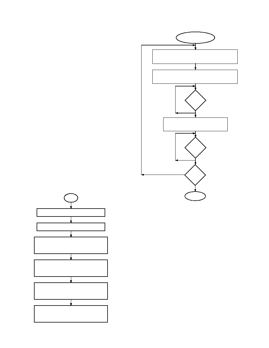
REV. 0
32
AD7708/AD7718
Configuring the AD7708/AD7718
All user-accessible registers on the AD7708 and AD7718 are
accessed via the serial interface. Communication with any of
these registers is initiated by first writing to the Communica-
tions Register. Figures 16, 17, and 18 show flow diagrams for
initializing the ADC, a sequence for calibrating the ADC chan-
nels, and a routine that cycles through and reads all channels.
Figure 16 shows a flowchart detailing necessary programming
steps required to initialize the ADC. The following are the general
programming steps required:
1. Configure and initialize the microcontroller or microprocessor
serial port.
2. Initialize the AD7708/AD7718 by configuring the following
registers:
a. IOCON to configure the digital I/O port.
b. FILTER to configure the update rate for each channel.
c. ADCCON to select the active input channel, select
the analog input range, and select unipolar or bipolar
operation.
d. MODE to configure the operating mode. The mode
register selects chop or nonchop operation, buffered/
unbuffered operation of the AINCOM input, 8-/10-
channel mode of operation and reference select along
with the selection of conversion, calibration or idle
modes of operation.
All operations consist of a write to the communications register
to specify the next operation as a write to a specified register.
Data is then written to the specified register. When each sequence
is complete, the ADC defaults to waiting for another write to
the communications register to specify the next operation.
WRITE TO COMMUNICATIONS REGISTER SETTING UP
NEXT OPERATION TO BE A WRITE TO THE MODE
REGISTER. CALIBRATE AND SELECT MODE OF
OPERATION
WRITE TO COMMUNICATIONS REGISTER SETTING UP
NEXT OPERATION TO BE A WRITE TO THE ADC
CONTROL REGISTER. CONFIGURE ADCCON
WRITE TO COMMUNICATIONS REGISTER SETTING UP
NEXT OPERATION TO BE A WRITE TO THE FILTER
REGISTER. SET SF WORD FOR REQUIRED
UPDATE RATE
WRITE TO COMMUNICATIONS REGISTER SELECTING
NEXT OPERATION TO BE A WRITE TO THE IOCON
REGISTER AND CONFIGURE THIS REGISTER
POWER-ON/RESET FOR AD7708/AD7718
CONFIGURE AND INITIALIZE C/ P SERIAL PORT
START
Figure 16. Initializing AD7708/AD7718
END
CAL
ANOTHER
CHANNEL
WRITE TO MODE REGISTER SELECTING
FULL-SCALE CALIBRATION
WRITE TO MODE REGISTER SELECTING
ZERO-SCALE CALIBRATION
WRITE TO ADCCON SELECTING CHANNEL AND CONFIGURING
INPUT RANGE AND UNIPOLAR/BIPOLAR MODE
CALIBRATION ROUTINE
MD BITS
= 001?
NO
YES
MD BITS
= 001?
NO
YES
YES
NO
Figure 17. Calibrating the AD7708/AD7718
Figure 17 shows a flowchart detailing necessary programming
steps required when calibrating the AD7708/AD7718. The
AD7708/AD7718 have dedicated calibration register pairs for
each of the fully-differential input channels. Having a dedicated
register pair per channel allows each channel to be calibrated as
part of the initialization and the ADC picks up the relevant
coefficients for each channel during normal operation. When
operating is pseudo-differential mode channels share calibration
register pairs. Channels that share coefficients should be config-
ured with the same operating conditions to avoid having to
calibrate each time a channel is switched, especially with chop
mode disabled. The AD7708/AD7718 are factory-calibrated
with chop mode enabled and, therefore, if the ADC is operated
at the same conditions as the factory-calibration field calibra-
tions will not be required. Extremely low offset error and offset
and gain drift errors are a by product of the chopping scheme.
When operating with chop mode disabled, the user can achieve
faster throughput times. An offset calibration is required with
chop disabled when a gain or temperature change occurs. The
following are the general programming steps required when
calibrating a channel on the AD7708/AD7718.
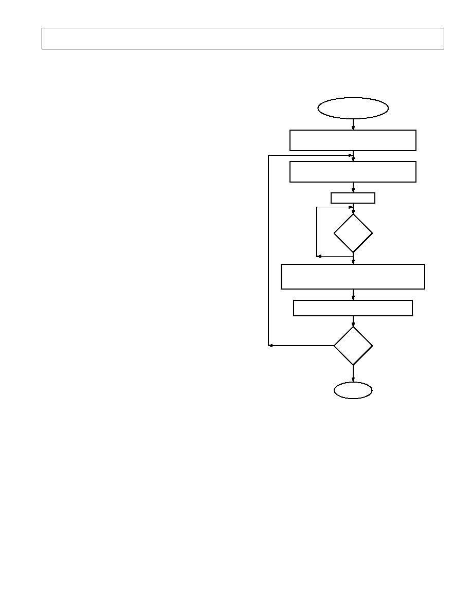
REV. 0
AD7708/AD7718
33
1. Write to the ADCCON register to select the channel to be
calibrated, its input range, and operation in unipolar or
bipolar mode.
2. Write to the mode register selecting chop or nonchop mode
of operation, select the reference, buffered/unbuffered opera-
tion on the AINCOM, and select zero-scale offset calibration.
Zero-scale calibration can be either self-calibration, where
the ADC determines the zero point internal to the ADC, or a
system calibration where the user must supply the zero-scale
voltage to the input for the duration of the calibration.
3. The calibration is initiated following the write to the mode
register. The user then needs to determine when the calibra-
tion is complete. This can be performed in two ways, by
polling the
RDY pin or flag or by monitoring the MD2,
MD1, MD0 bits in the mode register. These bits are reset to
0, 0, 1 when the calibration is complete. The flowchart uses
polling of the mode bits in the mode register to determine
when the calibration is complete.
4. The next step is to perform the full-scale calibration. Full-scale
calibration can be a self-calibration or system calibration.
Using system calibration the user must supply the full-scale
signal to the analog inputs for the duration of the calibration.
Again the MD2, MD1, MD0 bits in the mode register are
monitored to determine when the calibration is complete.
Figure 18 shows a flowchart detailing the necessary program-
ming steps required to cycle through and read data results from
all channels in a multiplexed application. This flowchart assumes
that all channels have been previously calibrated. The following
are the general programming steps required when reading all
channels in a multiplexed application.
1. The AD7708/AD7718 is put into continuous conversion
mode. In this mode the part continually converts on the
specified channel and the
RDY line indicates when valid
data is available to be read from the data register.
2. The ADCCON register is written to select the channel
for conversion, its input range and operation is unipolar/
bipolar mode.
3. In this flowchart hardware polling of the
RDY line is per-
formed to determine when it is valid to read data from the
converter. When
RDY is low, valid data is available in the
data register. The
RDY line is set high on a channel change
and will not go low until a new valid data word is available.
Alternatively, the RDY bit in the status register can be polled
in software to determine when to read data from the converter.
4. When the data is read, increment the channel address pointer
to select the next channel, poll the
RDY pin, or RDY bit in
the status register, and again read the data. Continue until all
channels have been read.
POLL RDY PIN
WRITE TO ADCCON SELECTING CHANNEL N
AND ITS OPERATING RANGE
END
WRITE TO COMMUNICATIONS REGISTER SETTING UP
NEXT OPERATION TO BE A READ OF DATA REGISTER
AND THEN READ DATA RESULT
WRITE TO MODE REGISTER SELECTING
CONTINUOUS CONVERSION MODE
CYCLE THROUGH AND
READ ALL CHANNELS
RDY
LOW?
NO
YES
ALL
CHANNELS
READ
NO
YES
INCREMENT CHANNEL ADDRESS (N = N+1)
Figure 18. Multichannel Read Operation

REV. 0
34
AD7708/AD7718
DIGITAL INTERFACE
As previously outlined, the AD7708/AD7718's programmable
functions are controlled using a set of on-chip registers. Data is
written to these registers via the part's serial interface and read
access to the on-chip registers is also provided by this interface.
All communications to the part must start with a write operation
to the Communications Register. After power-on or
RESET,
the device expects a write to its Communications Register. The
data written to this register determines whether the next operation
to the part is a read or a write operation and also determines to
which register this read or write operation occurs. Therefore,
write access to any of the other registers on the part starts with a
write operation to the Communications Register followed by a
write to the selected register. A read operation from any other
register on the part (including the output data register) starts
with a write operation to the Communications Register followed
by a read operation from the selected register.
The AD7708/AD7718s serial interface consists of five signals,
CS, SCLK, DIN, DOUT and RDY. The DIN line is used for
transferring data into the on-chip registers while the DOUT line
is used for accessing data from the on-chip registers. SCLK is
the serial clock input for the device and all data transfers (either
on DIN or DOUT) take place with respect to this SCLK signal.
The
RDY line is used as a status signal to indicate when data is
ready to be read from the devices's data register.
RDY goes low
when a new data word is available in the output register. It is
reset high when a read operation from the data register is complete.
It also goes high prior to the updating of the output register to
indicate when not to read from the device to ensure that a data
read is not attempted while the register is being updated.
CS is
used to select the device. It can be used to decode these devices in
systems where a number of parts are connected to the serial bus.
Figures 2 and 3 show timing diagrams for interfacing to the
AD7708/AD7718 with
CS used to decode the part. Figure 3 is
for a read operation from the AD7708/AD7718 output shift
register while Figure 2 shows a write operation to the input shift
register. It is possible to read the same data twice from the out-
put register even though the
RDY line returns high after the first
read operation. Care must be taken, however, to ensure that the
read operations have been completed before the next output
update is about to take place.
The serial interface can operate in three-wire mode by tying the
CS input low. In this case, the SCLK, DIN and DOUT lines
are used to communicate with the device and the status of the
RDY bit can be obtained by interrogating the STATUS Regis-
ter. This scheme is suitable for interfacing to microcontrollers. If
CS is required as a decoding signal, it can be generated from a
port bit. For microcontroller interfaces, it is recommended that
the SCLK idles high between data transfers.
The AD7708/AD7718 can also be operated with
CS used as a
frame synchronization signal. This scheme is suitable for DSP
interfaces. In this case, the first bit (MSB) is effectively clocked
out by
CS since CS would normally occur after the falling edge
of SCLK in DSPs. The SCLK can continue to run between
data transfers provided the timing numbers are obeyed.
The serial interface can be reset by exercising the
RESET input
on the part. It can also be reset by writing a series of 1s on the
DIN input. If a Logic 1 is written to the AD7708/AD7718 DIN
line for at least 32 serial clock cycles, the serial interface is reset.
This ensures that in three-wire systems, if the interface is lost
either via a software error or by some glitch in the system, it can
be reset back to a known state. This state returns the interface
to where the ADC is expecting a write operation to its Commu-
nications Register. This operation resets the contents of all
registers to their power-on-reset values.
Some microprocessor or microcontroller serial interfaces have a
single serial data line. In this case, it is possible to connect the
ADC's DOUT and DIN lines together and connect them to the
single data line of the processor. A 10 k
pull-up resistor should
be used on this single data line. In this case, if the interface is
lost, because the read and write operations share the same line,
the procedure to reset it back to a known state is somewhat
different than previously described. It requires a read operation
of 24 serial clocks followed by a write operation where a Logic
1 is written for at least 32 serial clock cycles to ensure that the
serial interface is back into a known state.
MICROCOMPUTER/MICROPROCESSOR INTERFACING
The flexible serial interface allows for easy interface to most
microcomputers and microprocessors. The flowcharts of Figures
16, 17, and 18 outline the sequence that should be followed
when interfacing a microcontroller or microprocessor to the
AD7708/AD7718. Figures 19, 20, and 21 show some typical
interface circuits.
The serial interface on the AD7708/AD7718 is capable of oper-
ating from just three wires and is compatible with SPI interface
protocols. The three-wire operation makes the part ideal for
isolated systems where minimizing the number of interface lines
minimizes the number of opto-isolators required in the system.
The serial clock input is a Schmitt-triggered input to accommo-
date slow edges from optocouplers. The rise and fall times of
other digital inputs to the AD7708/AD7718 should be no slower
than 1
µs.
Most of the registers on the AD7708/AD7718 are 8-bit regis-
ters, which facilitates easy interfacing to the 8-bit serial ports of
microcontrollers. The Data Register on the AD7718 is 24 bits
wide, the ADC data register on the AD7708 is 16 bits wide, and
the offset and gain registers are 16-bit registers on the AD7708
and 24-bit registers on the AD7718; however, data transfers to
these registers can consist of multiple 8-bit transfers to the serial
port of the microcontroller. DSP processors and microproces-
sors generally transfer 16 bits of data in a serial data operation.
Some of these processors, such as the ADSP-2105, have the
facility to program the amount of cycles in a serial transfer. This
allows the user to tailor the number of bits in any transfer to
match the register length of the required register in the AD7708/
AD7718.
Even though some of the registers on the AD7708/AD7718 are
only eight bits in length, communicating with two of these
registers in successive write operations can be handled as a
single 16-bit data transfer if required. For example, if the Filter
Register is to be updated, the processor must first write to the
Communications Register (saying that the next operation is a
write to the Filter Register) and then write eight bits to the Filter
Register. If required, this can all be done in a single 16-bit
transfer because once the eight serial clocks of the write opera-
tion to the Communications Register have been completed,
the part immediately sets itself up for a write operation to the
Filter Register.
REV. 0
AD7708/AD7718
35
AD7708/AD7718 to 68HC11 Interface
Figure 19 shows an interface between the AD7708/AD7718 and
the 68HC11 microcontroller. The diagram shows the minimum
(3-wire) interface with
CS on the AD7708/AD7718 hardwired
low. In this scheme, the RDY bit of the Status Register is
monitored to determine when the Data Register is updated.
An alternative scheme, which increases the number of inter-
face lines to four, is to monitor the
RDY output line from the
AD7708/AD7718. The monitoring of the
RDY line can be done
in two ways. First,
RDY can be connected to one of the 68HC11's
port bits (such as PC0), which is configured as an input. This
port bit is then polled to determine the status of
RDY. The
second scheme is to use an interrupt driven system, in which
case the
RDY output is connected to the IRQ input of the
68HC11. For interfaces that require control of the
CS input on
the AD7708/AD7718, one of the port bits of the 68HC11 (such
as PC1), which is configured as an output, can be used to drive
the
CS input.
68HC11
V
DD
SS
SCK
MISO
MOSI
RESET
SCLK
CS
DIN
DOUT
V
DD
AD7708/
AD7718
Figure 19. AD7708/AD7718-to-68HC11 Interface
The 68HC11 is configured in the master mode with its CPOL
bit set to a Logic 1 and its CPHA bit set to a Logic 1. When the
68HC11 is configured like this, its SCLK line idles high between
data transfers. The AD7708/AD7718 is not capable of full duplex
operation. If the AD7708/AD7718 is configured for a write
operation, no data appears on the DOUT lines even when the
SCLK input is active. Similarly, if the AD7708/AD7718 is config-
ured for a read operation, data presented to the part on the DIN
line is ignored even when SCLK is active.
AD7708/AD7718-to-8051 Interface
An interface circuit between the AD7708/AD7718 and the
8XC51 microcontroller is shown in Figure 20. The diagram
shows the minimum number of interface connections with
CS
on the AD7708/AD7718 hardwired low. In the case of the
8XC51 interface the minimum number of interconnects is just
two. In this scheme, the RDY bit of the Status Register is
monitored to determine when the Data Register is updated. The
alternative scheme, which increases the number of interface
lines to three, is to monitor the
RDY output line from the
AD7708/AD7718. The monitoring of the
RDY line can be done
in two ways. First,
RDY can be connected to one of the 8XC51's
port bits (such as P1.0) which is configured as an input. This
port bit is then polled to determine the status of
RDY. The
second scheme is to use an interrupt-driven system, in which
case the
RDY output is connected to the INT1 input of the
8XC51. For interfaces that require control of the
CS input on
the AD7708/AD7718, one of the port bits of the 8XC51 (such
as P1.1), which is configured as an output, can be used to drive
the
CS input. The 8XC51 is configured in its Mode 0 serial
interface mode. Its serial interface contains a single data line. As
a result, the DOUT and DIN pins of the AD7708/AD7718 should
be connected together with a 10 k
pull-up resistor. The serial
clock on the 8XC51 idles high between data transfers. The
8XC51 outputs the LSB first in a write operation, while the
AD7708/AD7718 expects the MSB first so the data to be trans-
mitted has to be rearranged before being written to the output
serial register. Similarly, the AD7708/AD7718 outputs the MSB
first during a read operation while the 8XC51 expects the LSB
first. Therefore, the data read into the serial buffer needs to be
rearranged before the correct data word from the AD7708/
AD7718 is available in the accumulator.
DV
DD
8XC51
AD7708/
AD7718
P3.0
P3.1
RESET
SCLK
CS
DIN
DOUT
DV
DD
10k
Figure 20. AD7708/AD7718-to-8XC51 Interface
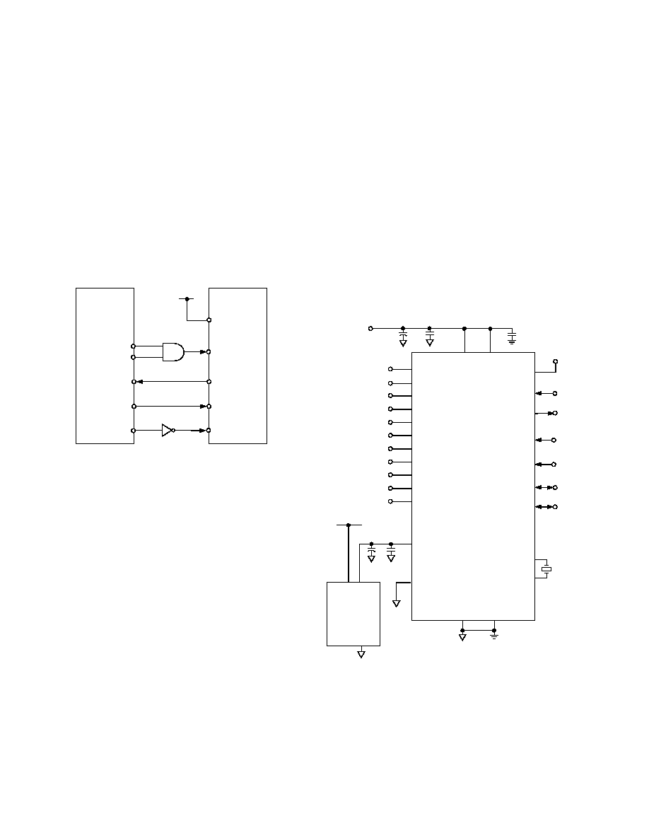
REV. 0
36
AD7708/AD7718
AD7708/AD7718-to-ADSP-2103/ADSP-2105 Interface
Figure 21 shows an interface between the AD7708/AD7718 and
the ADSP-2103/ADSP-2105 DSP processor. In the interface
shown, the RDY bit of the Status Register is again monitored to
determine when the Data Register is updated. The alternative
scheme is to use an interrupt-driven system, in which case the
RDY output is connected to the IRQ2 input of the ADSP-2103/
ADSP-2105. The serial interface of the ADSP-2103/ADSP-2105
is set up for alternate framing mode. The
RFS and TFS pins of
the ADSP-2103/ADSP-2105 are configured as active low outputs
and the ADSP-2103/ADSP-2105 serial clock line, SCLK, is also
configured as an output. The
CS for the AD7708/AD7718 is
active when either the
RFS or TFS outputs from the ADSP-2103/
ADSP-2105 are active. The serial clock rate on the ADSP-
2103/ADSP-2105 should be limited to 3 MHz to ensure correct
operation with the AD7708/AD7718.
DIN
RESET
DV
DD
CS
AD7708/
AD7718
SCLK
DOUT
SCLK
DT
DR
RFS
TFS
ADSP-2103 /
ADSP-2105
Figure 21. AD7708/AD7718-to-ADSP-2103/ADSP-2105
Interface
BASIC CONFIGURATION
The basic connection diagram for the AD7708/AD7718 in 10-
channel mode is shown in Figure 22. This shows both the AV
DD
and DV
DD
pins of the converters being driven from the analog
5 V supply. Some applications will have AV
DD
and DV
DD
driven
from separate supplies. AV
DD
and DV
DD
can be operated inde-
pendently of each other, allowing the device to be operated with
5 V analog supply and 3 V digital supply or vice versa. The parts
can be operated in 8- or 10-channel configurations. In 8-channel
mode the user has two reference input options. This allows the
user to operate some channels in ratiometric mode and others
in absolute measurement mode. In 10-channel mode only one
reference option is available. An AD780/REF195, precision 2.5 V
reference, provides the reference source for the part. A quartz
crystal or ceramic resonator provides the 32.768 kHz master
clock source for the part. In some cases, it will be necessary to
connect capacitors on the crystal or resonator to ensure that it
does not oscillate at overtones of its fundamental operating fre-
quency. The values of capacitors will vary, depending on the
manufacturer's specifications.
AD780 /
REF195
RECEIVE
(READ)
P1
P2
AIN6
AIN5
AIN4
AIN3
AIN2
AIN1
0.1 F
10 F
ANALOG 5V
SUPPLY
GND
V
IN
V
OUT
AGND
DGND
0.1 F
10 F
0.1 F
AV
DD
DV
DD
REF1IN(+)
REF1IN()
RESET
CS
DOUT
DIN
SCLK
MCLKIN
MCLKOUT
5V
CHIP
SELECT
SERIAL
DATA
(WRITE)
SERIAL
CLOCK
32kHz
CRYSTAL
ANALOG 5V
SUPPLY
AD7708/
AD7718
AIN8
AIN7
AIN9
AINCOM
AIN10
Figure 22. Basic Configuration for 10-Channel Mode
REV. 0
AD7708/AD7718
37
Analog Input Channels
The input multiplexer on AD7708/AD7718 can be configured
as either an 8- or 10-input channel device. This configuration is
selected using the CHCON bit in the MODE register. With
CHCON = 0 (Figure 23), the user has eight input channels; these
can be configured as eight pseudo-differential input channels with
respect to AINCOM or four fully-differential input channels.
In this configuration the user can select REFIN1 or REFIN 2 as
the reference for the selected channel using the REFSEL bit in
the mode register.
AIN6
AIN5
AIN4
AIN3
AIN2
AIN1
AD7708/
AD7718
AIN8
AIN7
REFIN1(+)
AINCOM
REFIN1()
REFIN2(+)
REFIN2()
AIN6
AIN5
AIN4
AIN3
AIN2
AIN1
AIN8
AIN7
REFIN1(+)
AINCOM
REFIN1()
REFIN2(+)
REFIN2()
Figure 23. Analog Input and Reference Options with
CHCON = 0
With CHCON = 1 (Figure 24), the user has 10 input channels
that can be configured as 10 pseudo-differential input channels
with respect to AINCOM or as five fully-differential input chan-
nels. The contents of the CHCON bit overrides the REFSEL
bit. If the ADC is configured in five fully-differential or 10 pseudo-
differential input channel mode, the REFSEL bit setting is
irrelevant as only REFIN1 is available. Channel selection Bits
CH3, CH2, CHI, and CH0 in the ADCCON register select the
input channel.
The input multiplexer switches the selected input channel to the
on-chip buffer amplifier and sigma-delta converter. When the
analog input channel is switched, the settling time of the part
must elapse before a new valid word is available from the ADC.
If any two inputs are configured as a differential input pair, this
input is buffered and the common-mode and absolute input volt-
age is restricted to a range between AGND + 100 mV and AV
DD
100 mV. Care must be taken in setting up the common-mode
voltage and input voltage range to ensure that these limits are
not exceeded, otherwise there will be a degradation in linearity
and noise performance.
AIN6
AIN5
AIN4
AIN3
AIN2
AIN1
AD7708/
AD7718
AIN8
AIN7
REFIN1(+)
AINCOM
REFIN1()
AIN9
AIN10
AIN6
AIN5
AIN4
AIN3
AIN2
AIN1
AIN8
AIN7
REFIN1(+)
AINCOM
REFIN1()
AIN9
AIN10
Figure 24. Analog Input and Reference Options with
CHCON = 1
Single-Ended Operation
The NEGBUF bit in the mode register is used to control the
operation of the input buffer on the AINCOM pin when config-
ured for pseudo-differential mode of operation. If cleared, the
analog negative input (AINCOM) is unbuffered. It should be
noted that the unbuffered input path on the AINCOM provides
a dynamic load to the driving source. Therefore, resistor/capacitor
combinations on this input pin can cause dc gain errors depend-
ing on the output impedance of the source that is driving the
AINCOM input. AINCOM is tied to AGND for single-ended
operation. This enables all pseudo-differential inputs to act as
single-ended analog inputs. All analog inputs still operate in
buffered mode and their common-mode and absolute input
voltage is restricted to a range between AGND + 100 mV and
AV
DD
100 mV.
Chop Mode of Operation (
CHOP = 0)
The signal chain on the AD7708/AD7718 can be operated with
chopping enabled or disabled. Chopping is enabled or disabled
using the
CHOP bit in the mode register. The default mode of
operation is for chop enabled (
CHOP = 0). Optimum perfor-
mance in terms of minimizing offset error and offset and gain
drift performance is achieved when chopping is enabled. The
digital filter decimation rate, and consequently the output data
rate, is programmable via the SF word loaded to the filter register.
Output data rates vary from 5.35 Hz (186.77 ms) to 105.03 Hz
(9.52 ms). The output data rate
f
f
SF
ADC
MOD
=
×
24
.
The overall frequency response from the digital filter with chop-
ping enabled is the product of a sinc
3
and a sinc response. There
are sinc
3
notches at integer multiples of 3
× f
ADC
and there are
sinc notches at odd integer multiples of f
ADC
/2. Normal mode
rejection is the major function of the digital filter on the AD7708/
AD7718. The normal mode 50
±1 Hz rejection with an SF word
of 82 is typically 100 dB. The 60
± 1 Hz rejection with SF = 68 is
typically 100 dB. Simultaneous 50 Hz and 60 Hz rejection of
better than 60 dB is achieved with an SF of 69 and gives a data
update rate of 19.8 Hz and a channel settling time of 101 ms. The
AD7708/AD7718 are factory-calibrated so field calibration will
only be required if the ADC is operated at temperatures that differ
substantially from the factory-calibration conditions.
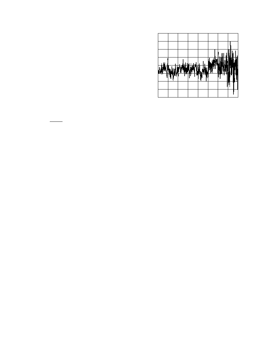
REV. 0
38
AD7708/AD7718
Nonchop Mode of Operation (
CHOP = 1)
Chopping is enabled and disabled using the
CHOP bit in the
mode register. Chopping is disabled by loading a 1 to the chop
bit in the mode register. With chopping disabled the available
output rates vary from 16.06 Hz (62.26 ms) to 1365.33 Hz (0.73 ms).
The range of applicable SF words is from 3 to 255. When the
chopping is disabled the channel output data rate is increased by a
factor of 3 compared to the situation when chopping is enabled
and using the same SF word. When used in multiplexed
applications, operation with chop disabled will offer the best
throughput time when cycling through all channels. The drawback
with chop disabled is that the drift performance is degraded
and calibration is required following a gain change or significant
temperature change. The output update and filter decimation
rate is again controlled by the SF word loaded to the filter
register. The digital filter frequency response places sinc
3
notches at integer multiples of the update rate. The output
update rate
f
f
SF
ADC
MOD
=
×
8
. The AD7708/AD7718 are targeted
at multiplexed applications and therefore operating with chop
disabled optimizes channel throughput time. One of the key
requirements in these applications is the selection of an SF word
so as to obtain the maximum filter rejection at 50 Hz and 60 Hz
while minimizing the channel throughput rate. This is achieved
with an SF word of 75 giving 57 dB rejection at 50 Hz, and
60 dB rejection at 60 Hz while offering a channel throughput
time of 55 ms. Using a higher SF word of 151, 50 Hz and
60 Hz rejection can be maximized at 60 dB with a channel
throughput rate of 110 ms. An SF word of 255 gives maximum
rejection at both 50 Hz and 60 Hz but the channel throughput
rate is restricted to 186 ms. Table XXI shows a quick comparison
of normal mode 50 Hz and 60 Hz rejection, settling time, and
update rate for a selection of SF words with chop both enabled
and disabled.
Programmable Gain Amplifier
The output from the buffer is applied to the input of the program-
mable gain amplifier (PGA). The PGA gain range is programmed
via the range bits in the ADCCON register. The PGA has eight
ranges. With an external 2.5 V reference applied, and a PGA
setting of 128, the unipolar analog input range is 0 mV to 20 mV,
while the bipolar analog input range is
±20 mV. With a PGA
setting of 1, the unipolar and bipolar input ranges are 2.56 V.
When operating with chop mode enabled (
CHOP = 0), the ADC
range-matching specification of 2
µV (typ) across all ranges
means that calibration need only be carried out on a single
range and does not have to be repeated when the PGA range is
changed. This is a significant advantage when compared with
similar ADCs available on the market. Typical matching across
ranges is shown in Figure 25. Here, the ADC is configured in
fully-differential, bipolar mode with an external 2.5 V reference,
while an analog input voltage of just greater than 19 mV is forced
on its analog inputs. The ADC continuously converts the dc
voltage at an update rate of 5.35 Hz, i.e., SF = FFhex, 800
conversion results in total are gathered. The first 100 results are
gathered with the ADC operating with a PGA setting of 128.
19.367
100
0
200
400
300
19.371
19.370
19.369
19.368
19.372
ADC INPUT
V
O
L
T
A
GE
mV
500
19.366
19.365
19.364
600
700
800
SAMPLE COUNT
ADC RANGE
20mV
40mV
80mV
160mV
320mV
640mV
1.28V
2.56V
Figure 25. ADC Range Matching
The PGA setting is then switched to 64 and 100 more results
are gathered, and so on until the last 100 samples are gathered
with a PGA setting of 1. From Figure 25, the variation in the sample
mean through each range, i.e., the range matching, is seen to be
of the order of 2
µV. When operating with chop mode disabled
(
CHOP = 1), new calibration data is needed (but not necessarily
a new calibration) to remove offset error when switching channels.
Bipolar/Unipolar Configuration
The analog inputs on the AD7708/AD7718 can accept either
unipolar or bipolar input voltage ranges. Bipolar input ranges
does not imply that the part can handle negative voltages with
respect to system AGND. Signals in pseudo-differential mode
are referenced to AINCOM, while in fully differential mode they
are referenced to the negative input of the differential input. For
example, if AINCOM is 2.5 V and the AD7708/AD7718 AIN1
analog input is configured for an analog input range of 0 mV to
+20 mV, the input voltage range on the AIN1 input is 2.5 V to
2.52 V. If AINCOM is 2.5 V and the AD7708/AD7718 is con-
figured for an analog input range of
±1.28 V, the analog input
range on the AIN1 input is 1.22 V to 3.78 V (i.e., 2.5 V
±
1.28 V). Bipolar or unipolar options are chosen by programming
U/
B bit in the ADCCON register. Programming for either
unipolar or bipolar operation does not change any of the input
signal conditioning; it simply changes the data output coding
and the points on the transfer function where calibrations occur.
Data Output Coding
When the AD7718 is configured for unipolar operation, the out-
put coding is natural (straight) binary with a zero differential
input voltage resulting in a code of 000 . . . 000, a midscale
voltage resulting in a code of 100 . . . 000, and a full-scale input
voltage resulting in a code of 111 . . . 111. The output code for
any analog input voltage can be represented as follows:
Code = (AIN
× GAIN × 2
24
)/(1.024
× V
REF
)
where
AIN is the analog input voltage,
GAIN is the PGA gain, i.e., 1 on the 2.5 V range and 128 on
the 20 mV range.

REV. 0
AD7708/AD7718
39
The output code for any analog input voltage on the AD7708
can be represented as follows:
Code = (AIN
× GAIN × 2
16
)/(1.024
× V
REF
)
where
AIN is the analog input voltage,
GAIN is the PGA gain, i.e., 1 on the 2.5 V range and 128 on
the 20 mV range.
When an ADC is configured for bipolar operation, the coding is
offset binary with a negative full-scale voltage resulting in a code
of 000 . . . 000, a zero differential voltage resulting in a code of
100 . . . 000, and a positive full-scale voltage resulting in a code
of 111 . . . 111. The output code from the AD7718 for any
analog input voltage can be represented as follows:
Code = 2
23
× [(AIN × GAIN/(1.024 × V
REF
)) + 1]
where
AIN is the analog input voltage,
GAIN is the PGA gain, i.e., 1 on the
±2.5 V range and 128 on
the
±20 mV range.
The output code from the AD7708 for any analog input voltage
can be represented as follows:
Code = 2
15
× [(AIN × GAIN/(1.024 × V
REF
)) + 1]
where
AIN is the analog input voltage,
GAIN is the PGA gain, i.e., 1 on the
±2.5 V range and 128 on
the
±20 mV range.
Oscillator Circuit
The AD7708/AD7718 is intended for use with a 32.768 kHz
watch crystal or ceramic resonator. A PLL internally locks onto
a multiple of this frequency to provide a stable 4.194304 MHz
clock for the ADC. The modulator sample rate is the same as
the oscillator frequency.
The start-up time associated with 32 kHz crystals is typically
300 ms. The OSPD bit in the mode register can be used to
prevent the oscillator from powering down when the AD7708/
AD7718 is placed in power-down mode. This avoids having to
wait 300 ms after exiting power-down to start a conversion at
the expense of raising the power-down current.
Reference Input
The AD7708/AD7718 has a fully differential reference input
capability. When the AD7708/AD7718 is configured in 8-channel
mode (CHCON = 0) the user has the option of selecting one of
two reference options. This allows the user to configure some
channels, for example, for ratiometric operation while others can
be configured for absolute value measurements. The REFSEL bit
in the mode register allows selection of the required reference.
If the REFSEL bit is cleared, the reference selected is REFIN1(+)
REFIN1() for the active channel. If this bit is set, the refer-
ence selected is REFIN2(+) REFIN2() for the active channel.
When the AD7708/AD7718 is configured in 10-channel mode
(CHCON = 1) the user has only one reference option (REFIN1).
The contents of the CHCON bit overrides the REFSEL bit. If
the ADC is configured in five fully-differential or 10 pseudo-
differential input channel mode, the REFSEL bit setting is
irrelevant as only one reference input is available.
The common-mode range for these differential inputs is from
AGND to AV
DD
. The reference inputs are unbuffered and
therefore excessive R-C source impedances will introduce gain
errors. The nominal reference voltage for specified operation,
VREF, (REFIN1(+)REFIN1() or REFIN2(+)REFIN2()),
is 2.5 V, but the AD7708/AD7718 is functional with reference
voltages from 1 V to AV
DD
. In applications where the excitation
(voltage or current) for the transducer on the analog input also
drives the reference voltage for the part, the effect of the low
frequency noise in the excitation source will be removed as the
application is ratiometric. If the AD7708/AD7718 is used in a
nonratiometric application, a low noise reference should be
used. Recommended reference voltage sources for the AD7708/
AD7718 include the AD780, REF43, and REF192. It should
also be noted that the reference inputs provide a high impedance,
dynamic load. Because the input impedance of each reference
input is dynamic, resistor/capacitor combinations on these inputs
can cause dc gain errors, depending on the output impedance of
the source that is driving the reference inputs. Reference voltage
sources, like those recommended above (e.g., AD780) will typically
have low output impedances and are therefore tolerant of having
decoupling capacitors on the REFIN(+) without introducing gain
errors in the system. Deriving the reference input voltage across
an external resistor will mean that the reference input sees a
significant external source impedance. External decoupling on
the REFIN(+) and REFIN() pins would not be recommended
in this type configuration.
RESET Input
The
RESET input on the AD7708/AD7718 resets all the logic,
the digital filter and the analog modulator while all on-chip
registers are reset to their default state.
RDY is driven high and
the AD7708/AD7718 ignores all communications to any of its
registers while the
RESET input is low. When the RESET input
returns high the AD7708/AD7718 operates with its default setup
conditions and it is necessary to set up all registers and carry out
a system calibration if required after a
RESET command.
Power-Down Mode
Loading 0, 0, 0 to the MD2, MD1, MD0 bits in the ADC mode
register places the ADC in device power-down mode. Device
power-down mode is the default condition for the AD7708/
AD7718 on power-up. The ADC retains the contents of all its
on-chip registers (including the data register) while in power-
down. The device power-down mode does not affect the digital
interface, but does affect the status of the
RDY pin. Writing the
AD7708/AD7718 into power-down will reset the
RDY line high.
Placing the part in power-down mode reduces the total current
(AI
DD
+ DI
DD
) to 31
µA max when the part is operated at 5 V
and the oscillator allowed to run during power-down mode.
With the oscillator shut down the total I
DD
is typically 9
µA.

REV. 0
40
AD7708/AD7718
Calibration
The AD7708/AD7718 provides four calibration modes that can
be programmed via the mode bits in the mode register. One of
the major benefits of the AD7708/AD7718 is that it is factory-
calibrated with chopping enabled as part of the final test process
with the generated coefficients stored within the ADC. At power-
on, the factory gain calibration coefficients are automatically
loaded to the gain calibration registers on the AD7708/AD7718.
This gives excellent offset and drift performance and it is
envisaged that in the majority of applications the user will not
need to perform any field calibrations. Also, because factory
gain calibration coefficients (generated at 25
°C ambient) are
automatically present at power-on, an internal full-scale calibration
will only be required if the part is being operated at temperatures
significantly different from 25
°C.
When chopping is disabled (
CHOP =1) the AD7708/AD7718
requires an offset calibration or new calibration coefficients on
range changing or when significant temperature changes occur
as the signal chain is no longer chopped and offset and drift
errors are no longer removed as part of the conversion process.
The factory-calibration values for any one channel will be over-
written if any one of the four calibration options is initiated.
The AD7708/AD7718 offers "internal" or "system" calibration
facilities. For full calibration to occur, the calibration logic must
record the modulator output for two different input conditions.
These are "zero-scale" and "full-scale" points. These points
are derived by performing a conversion on the different input
voltages provided to the input of the modulator during calibration.
The result of the "zero-scale" calibration conversion is stored in
the Offset Calibration Registers for the appropriate channel.
The result of the "full-scale" calibration conversion is stored
in the Gain Calibration Registers. With these readings, the
calibration logic can calculate the offset and the gain slope for
the input-to-output transfer function of the converter. During an
"internal" zero-scale or full-scale calibration, the respective
"zero" input and "full-scale" input are automatically connected
to the ADC input pins internally to the device. A "system" cali-
bration, however, expects the system zero-scale and system
full-scale voltages to be applied to the external ADC pins
before the calibration mode is initiated. In this way external
ADC errors are taken into account and minimized as a result
of system calibration. It should also be noted that to optimize
calibration accuracy, all AD7708/AD7718 ADC calibrations
are carried out automatically at the slowest update rate with
chop enabled. When chop mode is disabled calibrations are
carried out at the update rate defined by the SF word in the
filter register.
Internally in the AD7708/AD7718, the coefficients are normalized
before being used to scale the words coming out of the digital
filter. The offset calibration coefficient is subtracted from the
result prior to the multiplication by the gain coefficient. With
chopping disabled AD7708/AD7718 ADC specifications will
only apply after a zero-scale calibration at the operating point of
interest. From an operational point of view, a calibration should
be treated like another ADC conversion. A zero-scale calibration
(if required) should always be carried out before a full-scale
calibration. System software should monitor the RDY bit in the
STATUS register to determine end of calibration via a polling
sequence or interrupt driven routine.
Grounding and Layout
Since the analog inputs and reference inputs are differential,
most of the voltages in the analog modulator are common-mode
voltages. The excellent common-mode rejection of the part will
remove common-mode noise on these inputs. The analog and
digital supplies to the AD7708/AD7718 are independent and
separately pinned out to minimize coupling between the analog
and digital sections of the device. The AD7708/AD7718 can be
operated with 5 V analog and 3 V digital supplies or vice versa.
The digital filter will provide rejection of broadband noise on
the power supplies, except at integer multiples of the modulator
sampling frequency. The digital filter also removes noise from
the analog and reference inputs provided these noise sources do
not saturate the analog modulator. As a result, the AD7708/
AD7718 is more immune to noise interference than a conventional
high-resolution converter. However, because the resolution of the
AD7708/AD7718 is so high and the noise levels from the
converter so low, care must be taken with regard to grounding
and layout.
The printed circuit board that houses the ADC should be designed
so the analog and digital sections are separated and confined to
certain areas of the board. This facilitates the use of ground planes
that can be easily separated. A minimum etch technique is
generally best for ground planes as it gives the best shielding.
Although the AD7708/AD7718 has separate pins for analog and
digital ground, the AGND and DGND pins are tied together
internally via the substrate. Therefore, the user must not tie
these two pins to separate ground planes unless the ground
planes are connected together near the AD7708/AD7718.
In systems where the AGND and DGND are connected some-
where else in the system, i.e., the systems power supply, they
should not be connected again at the AD7708/AD7718 or a
ground loop will result. In these situations it is recommended that
ground pins of the AD7708/AD7718 be tied to the AGND plane.
In any layout it is implicit that the user keep in mind the flow of
currents in the system, ensuring that the paths for all currents
are as close as possible to the paths the currents took to reach
their destinations. Avoid forcing digital currents to flow through
the AGND.
Avoid running digital lines under the device as these will couple
noise onto the die. The analog ground plane should be allowed
to run under the AD7708/AD7718 to prevent noise coupling.
The power supply lines to the AD7708/AD7718 should use as
wide a trace as possible to provide low impedance paths and
reduce the effects of glitches on the power supply line. Fast
switching signals like clocks should be shielded with digital
ground to avoid radiating noise to other sections of the board
and clock signals should never be run near the analog inputs.
Avoid crossover of digital and analog signals. Traces on opposite
sides of the board should run at right angles to each other. This will
reduce the effects of feedthrough through the board. A microstrip
technique is by far the best, but is not always possible with a
double-sided board. In this technique, the component side of
the board is dedicated to ground planes while signals are placed
on the solder side.
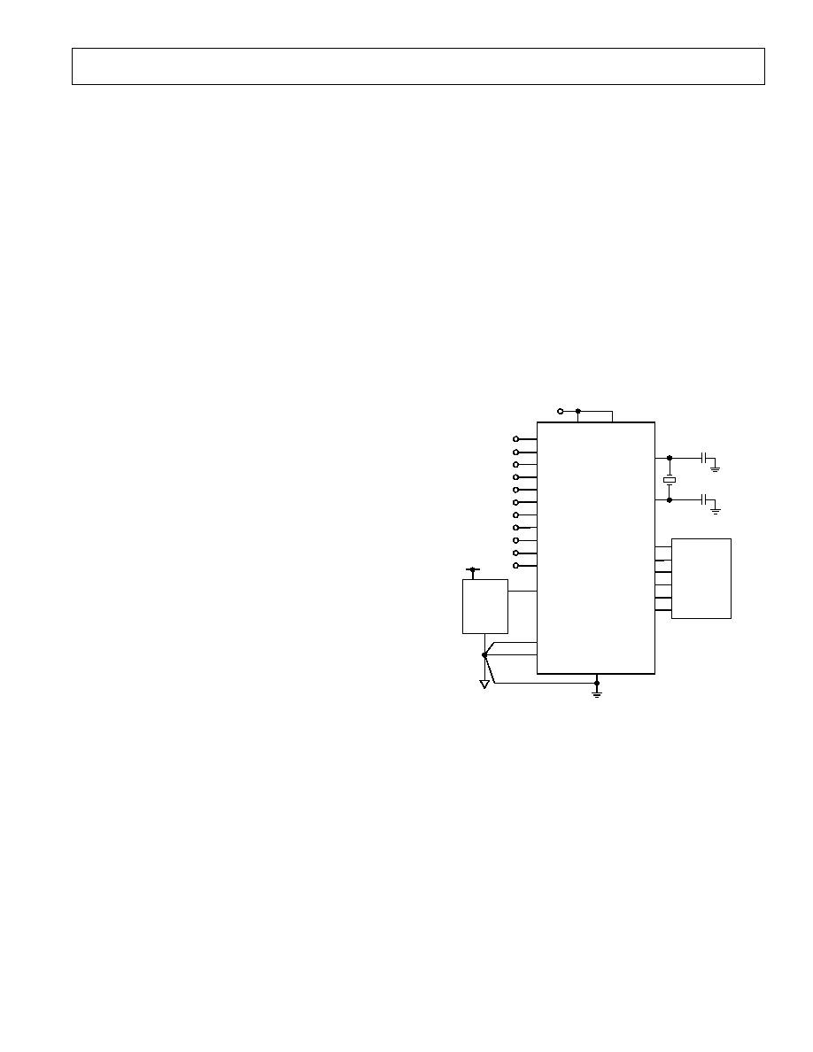
REV. 0
AD7708/AD7718
41
Good decoupling is important when using high resolution ADCs.
All analog supplies should be decoupled with 10
µF tantalum in
parallel with 0.1
µF capacitors to AGND. To achieve the best
from these decoupling components, they have to be placed
as close as possible to the device, ideally right up against the
device. All logic chips should be decoupled with 0.1
µF ceramic
capacitors to DGND. In systems where a common supply
voltage is used to drive both the AV
DD
and DV
DD
of the AD7708/
AD7718, it is recommended that the system's AV
DD
supply is
used. This supply should have the recommended analog supply
decoupling capacitors between the AV
DD
pin of the AD7708/
AD7718 and AGND and the recommended digital supply
decoupling capacitor between the DV
DD
pin of the AD7708/
AD7718 and DGND.
APPLICATIONS
The AD7708/AD7718 provides a low cost, high resolution
analog-to-digital function. The AD7708 offers 16-bit resolution
while the AD7718 offers 24-bit resolution. The AD7708 and
AD7718 are pin and function compatible. The AD7718 allows a
direct upgradable path from a 16-bit to a 24-bit system with
minimal software and no hardware changes. Because the analog-
to-digital function is provided by a sigma-delta architecture, it
makes the part more immune to noisy environments, thus mak-
ing the part ideal for use in sensor measurement and in industrial
and process control applications. There are two modes of operation
associated with the AD7708/AD7718, chop enabled (
CHOP = 0)
or chop disabled (
CHOP = 1). With chop enabled the signal chain
is chopped and the device is factory-calibrated at final test in
this mode. Field calibration can be avoided due to the extremely
low offset and gain drifts exhibited by the converter in this
mode. While operating in this mode gives optimum performance
in terms of offset error and offset and gain drift performance, it
offers limited throughput when cycling through all channels.
With chopping disabled, the signal chain is not chopped and
therefore the user needs to ensure that the ADC is calibrated on
range changes and if there is a significant temperature change
as the gain and offset drift performance is degraded.
The key advantage in using the AD7708/AD7718 with chopping
disabled is in channel cycling applications where system through-
put is of prime importance. The max conversion rate with chop
disabled is 1.36 kHz compared with 105 Hz with chop enabled.
The AD7708/AD7718 also provides a programmable gain ampli-
fier, a digital filter, and system calibration options. Thus, it
provides far more system level functionality than off-the-shelf
integrating ADCs without the disadvantage of having to sup-
ply a high quality integrating capacitor. In addition, using the
AD7708/AD7718 in a system allows the system designer to
achieve a much higher level of resolution because noise perfor-
mance of the AD7708/AD7718 is significantly better than that
of integrating ADCs.
The on-chip PGA allows the AD7708/AD7718 to handle an
analog input voltage range as low as 10 mV full scale with V
REF
= 1.25 V. The AD7708/AD7718 can be operated in 8-channel
mode with two reference input options or 10-channel mode with
one reference input. Eight-channel mode allows both ratiometric
or absolute measurements to be performed on any channel using
the two reference input options. The differential analog inputs
of the part allow this analog input range to have an absolute
value anywhere between AGND + 100 mV and AV
DD
100 mV.
The buffer on the negative analog input can be bypassed allowing
the AD7708/AD7718 be operated as eight or ten single-ended
input channels. The PGA allows the user to connect transducers
directly to the input of the AD7708/AD7718. The program-
mable gain front end on the AD7708/AD7718 allows the part to
handle unipolar analog input ranges from 0 mV to +20 mV to
0 V to +2.5 V and bipolar inputs of
±20 mV to ±2.5 V. Because
the part operates from a single supply these bipolar ranges are
with respect to a biased-up differential input.
Data Acquisition
The AD7708/AD7718, with its different configuration options
(five fully-differential input or 10 pseudo-differential input
channels with one reference input or four fully-differential input
or eight pseudo-differential input channels with two reference
inputs), is suited to low bandwidth, high resolution data acquisi-
tion systems. In addition, the 3-wire digital interface allows this
data acquisition front end to be isolated with just three opto-
isolators. The entire system can be operated from a single 3 V
or 5 V supply, provided that the input signals to the AD7708/
AD7718's analog inputs are all of positive polarity.
5V
AD780
AIN6
AIN5
AIN4
AIN3
AIN2
AIN1
5V
GND
V
IN
V
OUT
AGND
DGND
AV
DD
DV
DD
REF1IN()
MCLKIN
MCLKOUT
32kHz
AD7708/
AD7718
AIN8
AIN7
AIN9
AINCOM
AIN10
MICRO-
CONTROLLER
SCLK
CS
DIN
DOUT
RDY
RESET
REFIN1(+)
Figure 26. Data Acquisition Using the AD7708/AD7718
Programmable Logic Controllers
The AD7708/AD7718 is also suited to programmable logic
controller applications. In such applications, the ADC is required
to handle signals from a variety of different transducers. The
AD7708/AD7718's programmable gain front end allows the
part to either handle low level signals directly from a transducer
or full-scale signals that have already been conditioned. The faster
throughput rate and settling time of the part when operated with
chopping disabled makes this the optimum mode of operation in
PLC applications as an important feature in these applications is
loop response time. The configuration of the AD7708/AD7718
in PLC applications is similar to that outlined for a data acquisi-
tion system and is shown in Figure 26. In this application the
AD7708/AD7718 is configured in 10-channel mode, (CHCON
= 1) and can be operated as 10 pseudo-differential inputs with
respect to AINCOM or as five fully-differential input channels.
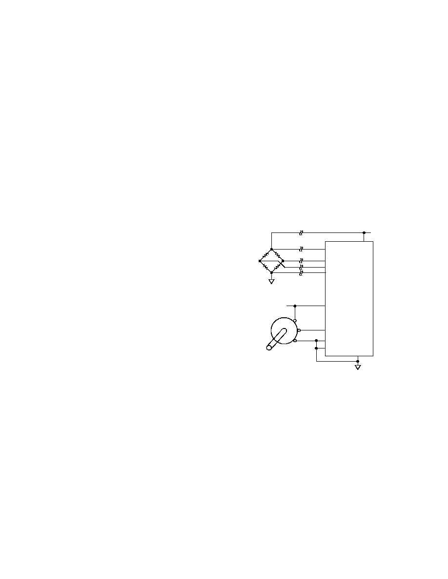
REV. 0
42
AD7708/AD7718
Converting Single-Ended Inputs
The AD7708/AD7718 generally operates in buffered mode. This
places a restriction of AGND + 100 mV to AVDD 100 mV on
the absolute and common-mode voltages that can be applied to
any input on the AD7708/AD7718.
Some applications may require the measurement of analog
inputs with respect to AGND. To enable the AD7708/AD7718
to be used in these single-ended applications, the buffer on the
AINCOM can be bypassed. The NEGBUF bit in the mode
register controls the operation of the input buffer on the AINCOM
input when a channel is configured for pseudo-differential mode of
operation. If cleared, the analog negative input (AINCOM) is
unbuffered, allowing it to be tied to AGND in single-ended
input configuration. If this bit is set, the analog negative input
(AINCOM) is buffered, placing a restriction on its common-
mode input range. When AINCOM is unbuffered, signals with a
common-mode range from AGND 30 mV to AVDD + 30 mV
can be accommodated on this input allowing the end user to
connect the AINCOM input to AGND and perform single-
ended measurements with respect to this input. This unbuffered
input path on the AINCOM provides a dynamic load to the
driving source. Therefore, resistor/capacitor combinations on
this input pin can cause dc gain errors, depending on the output
impedance of the source that is driving the AINCOM input. All
analog inputs still operate in buffered mode and their com-
mon-mode and absolute input voltage is restricted to a range
between AGND + 100 mV and AV
DD
100 mV.
Combined Ratiometric and Absolute Value Measurement
System
The AD7708/AD7718 when operated with CHCON = 0 can be
configured for operation as four fully-differential analog inputs or
eight pseudo-differential analog inputs with two fully-differential
reference inputs. Having the ability to use either REFIN1 or
REFIN2 with any channel during the conversion process allows
the end user to make both absolute and ratiometric measure-
ments as shown in Figure 27. In this example a fully-differential
analog input (AIN1AIN2) is being converted from a bridge trans-
ducer in a ratiometric manner using REFIN1 as the reference
input for this channel. AIN3 is configured as a pseudo-differential
input channel using REFIN2 to perform an absolute measurement
on the potentiometer. The REFSEL bit in the mode register is
used to select which reference is used with the active channel
during the conversion process. When the AD7708/AD7718 is
configured with CHCON = 1, only one reference (REFIN1) is
available. The contents of the CHCON bit override the REFSEL
bit. If the ADC is configured in five fully-differential or 10
pseudo-differential input channel mode, the REFSEL bit setting
is irrelevant as only REFIN1 is available.
REFIN1()
AD7718
REFIN2(+)
REFIN1(+)
AINCOM
AIN1
AIN3
AIN2
REFIN2()
GND
EXCITATION VOLTAGE = 4V
WIPER
Figure 27. Absolute and Ratiometric Measurement
System Using AD7718
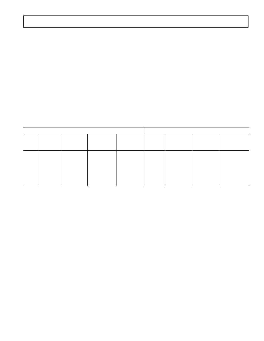
REV. 0
AD7708/AD7718
43
Table XXI. Normal Mode 50 Hz and 60 Hz Rejection vs. Settling Time and Update Rate for a Selection of SF Words
CHOP Disabled
CHOP Enabled
50 Hz
1 Hz
60 Hz
1 Hz
50 Hz
1 Hz
60 Hz
1 Hz
SF
Rejection
Rejection
Rejection
Rejection
Word
f
ADC
(Hz)
t
SETTLE
(ms)
(dB)
(dB)
f
ADC
(Hz)
t
SETTLE
(ms) (dB)
(dB)
03
1365.33
2.20
0.05
0.08
N/A
N/A
N/A
N/A
13
315.08
9.52
1
1.5
105.03
19.04
21
13.6
69
59.36
50.54
42
94
19.79
101
60
94
75
54.6
54.93
57
60
18.2
110
62
66
82
49.95
60
100
16.65
180
100
53
151
27.13
110.6
60
60
9.04
221
72
63
255
16.06
186.76
77
68
5.35
373.5
93
68
Optimizing Throughput while Maximizing 50 Hz and 60 Hz
Rejection in a Multiplexed Data Acquisition System
The AD7708/AD7718 can be optimized for one of two modes
of operation. Operating the AD7708/AD7718 with chopping
enabled (
CHOP = 0) optimizes the AD7708/AD7718 for analog
performance over channel throughput. Output data rates vary
from 5.35 Hz (186.77 ms) to 105.03 Hz (9.52 ms). Optimum
performance, in terms of minimizing offset error and offset and
gain drift performance, is achieved as a result of chopping the
signal chain.
With chopping disabled the available output rates vary from
16.06 Hz (62.26 ms) to 1365.33 Hz (0.73 ms). The range of
applicable SF words is from 3 to 255. When the chopping is
disabled the channel output data rate is increased by a factor of
3 compared to the situation when chopping is enabled is
disabled. When used in multiplexed applications, operation
with chop disabled will offer the best throughput time when
cycling through all channels. The drawback with chopping
disabled is that the drift performance is degraded and calibra-
tion is required following gain and temperature changes. One
of the key requirements in these applications is to optimize the SF
word to obtain the maximum filter rejection at 50 Hz and 60 Hz
while minimizing the channel throughput rate. This is achieved
with an SF word of 75 giving 57 dB rejection at 50 Hz and
60 dB rejection at 60 Hz while offering a channel throughput
time of 55 ms.
Using a higher SF word of 151, 50 Hz and 60 Hz rejection can
be maximized at 60 dB with a channel throughput rate of 110 ms.
An SF word of 255 gives maximum rejection at both 50 Hz
and 60 Hz, but the channel throughput rate is restricted to
186 ms. Table XXI gives a quick comparison of normal mode 50 Hz
and 60 Hz rejection, settling time, and update rate for a selec-
tion of SF words with both chopping enabled and disabled.
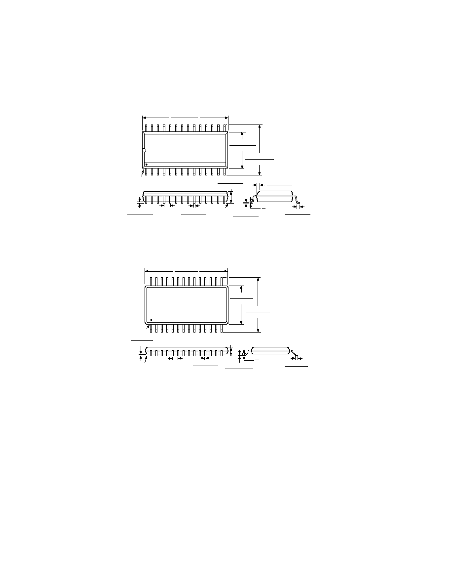
REV. 0
44
C0183117/01(0)
PRINTED IN U.S.A.
AD7708/AD7718
28-Lead Plastic SOIC
(R-28)
0.0125 (0.32)
0.0091 (0.23)
8
0
0.0291 (0.74)
0.0098 (0.25)
45
0.0500 (1.27)
0.0157 (0.40)
SEATING
PLANE
0.0118 (0.30)
0.0040 (0.10)
0.0192 (0.49)
0.0138 (0.35)
0.1043 (2.65)
0.0926 (2.35)
0.0500
(1.27)
BSC
28
15
14
1
0.7125 (18.10)
0.6969 (17.70)
0.4193 (10.65)
0.3937 (10.00)
0.2992 (7.60)
0.2914 (7.40)
PIN 1
28-Lead Plastic TSSOP
(RU-28)
0.177 (4.50)
0.169 (4.30)
28
15
14
1
0.386 (9.80)
0.378 (9.60)
0.256 (6.50)
0.246 (6.25)
PIN 1
SEATING
PLANE
0.006 (0.15)
0.002 (0.05)
0.0118 (0.30)
0.0075 (0.19)
0.0256 (0.65)
BSC
0.0433 (1.10)
MAX
0.0079 (0.20)
0.0035 (0.090)
0.028 (0.70)
0.020 (0.50)
8
0
OUTLINE DIMENSIONS
Dimensions shown in inches and (mm).
Document Outline
- Specifications
- Pinout
- Package drawings
- Ordering Guide
- Features
- Applications
- Product Description
- Timing characteristics
- Functional Block Diagram
- Functional Block Diagram
- Pin Function Description
- Circuit Description
-
Typical Performance Characteristics
- TABLE OF CONTENTS
- CAUTION
- ADC CIRCUIT INFORMATION
- ADC NOISE PERFORMANCE CHOP ENABLED (CHOP = 0)
- ADC NOISE PERFORMANCE CHOP DISABLED (CHOP = 1)
- ON-CHIP REGISTERS
- AD7718 ADC (DATA)
- AD7708 (DATA)
- AD7718
- AD7708
- AD7718
- DIGITAL INTERFACE
- MICROCOMPUTER/MICROPROCESSOR INTERFACING
- APPLICATIONS
- DIAGRAMS
- Load Circuit for Timing Characterization
- Write Cycle Timing Diagram
- Read Cycle Timing Diagram
- ADC Channel Block Diagram with CHOP Enabled
- ADC Channel Block Diagram with CHOP Disabled
- On-Chip Registers
- Calibrating the AD7708/AD7718
- Initializing AD7708/AD7718
- Multichannel Read Operation
- AD7708/AD7718-to-68HC11 Interface
- AD7708/AD7718-to-8XC51 Interface
- AD7708/AD7718-to-ADSP-2103/ADSP-2105 Interface
- Basic Configuration for 10-Channel Mode
- Analog Input and Reference Options with CHCON = 0
- Analog Input and Reference Options with CHCON = 1
- Data Acquisition Using the AD7708/AD7718
- Absolute and Ratiometric Measurement System Using AD7718