Äîêóìåíòàöèÿ è îïèñàíèÿ www.docs.chipfind.ru
REV. B
Information furnished by Analog Devices is believed to be accurate and
reliable. However, no responsibility is assumed by Analog Devices for its
use, nor for any infringements of patents or other rights of third parties
which may result from its use. No license is granted by implication or
otherwise under any patent or patent rights of Analog Devices.
a
AD7755*
One Technology Way, P.O. Box 9106, Norwood, MA 02062-9106, U.S.A.
Tel: 781/329-4700
World Wide Web Site: http://www.analog.com
Fax: 781/326-8703
© Analog Devices, Inc., 2000
Energy Metering IC
with Pulse Output
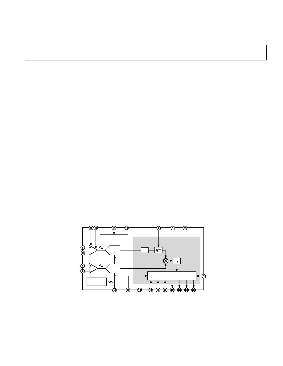
FUNCTIONAL BLOCK DIAGRAM
MULTIPLIER
AC/
DC
CLKOUT
V1P
V1N
G0
V2P
G1
AV
DD
DV
DD
HPF
CLKIN
REF
IN/OUT
F1
F2
CF
REVP
SCF
S0
S1
RESET
AGND
DGND
PHASE
CORRECTION
4k
...
110101
...
SIGNAL
PROCESSING
BLOCK
ADC
PGA
x1, x2, x8, x16
POWER
SUPPLY MONITOR
ADC
V2N
AD7755
...
11011001
...
LPF
2.5V
REFERENCE
DIGITAL-TO-FREQUENCY
CONVERTER
FEATURES
High Accuracy, Supports 50 Hz/60 Hz IEC 687/1036
Less than 0.1% Error Over a Dynamic Range of
500 to 1
The AD7755 Supplies
Average Real Power on the
Frequency Outputs F1 and F2
The High Frequency Output CF Is Intended for
Calibration and Supplies
Instantaneous Real Power
The Logic Output REVP Can Be Used to Indicate a
Potential Miswiring or Negative Power
Direct Drive for Electromechanical Counters and
Two Phase Stepper Motors (F1 and F2)
A PGA in the Current Channel Allows the Use of Small
Values of
Shunt and Burden Resistance
Proprietary ADCs and DSP Provide High Accuracy over
Large Variations in Environmental Conditions and
Time
On-Chip Power Supply Monitoring
On-Chip Creep Protection (No Load Threshold)
On-Chip Reference 2.5 V 6 8% (30 ppm/8C Typical)
with External Overdrive Capability
Single 5 V Supply, Low Power (15 mW Typical)
Low Cost CMOS Process
GENERAL DESCRIPTION
The AD7755 is a high accuracy electrical energy measurement
IC. The part specifications surpass the accuracy requirements
as quoted in the IEC1036 standard. See Analog Devices'
Application Note AN-559 for a description of an IEC1036
watt-hour meter reference design.
The only analog circuitry used in the AD7755 is in the ADCs
and reference circuit. All other signal processing (e.g., multipli-
cation and filtering) is carried out in the digital domain. This
approach provides superior stability and accuracy over extremes
in environmental conditions and over time.
The AD7755 supplies average real power information on the
low frequency outputs F1 and F2. These logic outputs may be
used to directly drive an electromechanical counter or interface
to an MCU. The CF logic output gives instantaneous real power
information. This output is intended to be used for calibration
purposes, or interfacing to an MCU.
The AD7755 includes a power supply monitoring circuit on the
AV
DD
supply pin. The AD7755 will remain in a reset condition
until the supply voltage on AV
DD
reaches 4 V. If the supply falls
below 4 V, the AD7755 will also be reset and no pulses will be
issued on F1, F2 and CF.
Internal phase matching circuitry ensures that the voltage and
current channels are phase matched whether the HPF in Chan-
nel 1 is on or off. An internal no-load threshold ensures that the
AD7755 does not exhibit any creep when there is no load.
The AD7755 is available in 24-lead DIP and SSOP packages.
*U.S. Patents 5,745,323, 5,760,617, 5,862,069, 5,872,469.

REV. B
2
AD7755SPECIFICATIONS
(AV
DD
= DV
DD
= 5 V 5%, AGND = DGND = 0 V, On-Chip Reference, CLKIN = 3.58 MHz,
T
MIN
to T
MAX
= 40 C to +85 C)
Parameter
A Version
B Version
Unit
Test Conditions/Comments
ACCURACY
1, 2
Measurement Error
1
on Channel 1
Channel 2 with Full-Scale Signal (
±660 mV), 25°C
Gain = 1
0.1
0.1
% Reading typ
Over a Dynamic Range 500 to 1
Gain = 2
0.1
0.1
% Reading typ
Over a Dynamic Range 500 to 1
Gain = 8
0.1
0.1
% Reading typ
Over a Dynamic Range 500 to 1
Gain = 16
0.1
0.1
% Reading typ
Over a Dynamic Range 500 to 1
Phase Error
1
Between Channels
Line Frequency = 45 Hz to 65 Hz
V1 Phase Lead 37
°
(PF = 0.8 Capacitive)
±0.1
±0.1
Degrees(
°) max AC/DC = 0 and AC/DC = 1
V1 Phase Lag 60
°
(PF = 0.5 Inductive)
±0.1
±0.1
Degrees(
°) max AC/DC = 0 and AC/DC = 1
AC Power Supply Rejection
1
AC/
DC = 1, S0 = S1 = 1, G0 = G1 = 0
Output Frequency Variation (CF)
0.2
0.2
% Reading typ
V1 = 100 mV rms, V2 = 100 mV rms, @ 50 Hz
Ripple on AV
DD
of 200 mV rms @ 100 Hz
DC Power Supply Rejection
1
AC/
DC = 1, S0 = S1 = 1, G0 = G1 = 0
Output Frequency Variation (CF)
±0.3
±0.3
% Reading typ
V1 = 100 mV rms, V2 = 100 mV rms,
AV
DD
= DV
DD
= 5 V
± 250 mV
ANALOG INPUTS
See Analog Inputs Section
Maximum Signal Levels
± 1
± 1
V max
V1P, V1N, V2N and V2P to AGND
Input Impedance (DC)
390
390
k
min
CLKIN = 3.58 MHz
Bandwidth (3 dB)
14
14
kHz typ
CLKIN/256, CLKIN = 3.58 MHz
ADC Offset Error
1, 2
±25
±25
mV max
Gain = 1, See Terminology and Performance Graphs
Gain Error
1
± 7
± 7
% Ideal typ
External 2.5 V Reference, Gain = 1
V1 = 470 mV dc, V2 = 660 mV dc
Gain Error Match
1
±0.2
±0.2
% Ideal typ
External 2.5 V Reference
REFERENCE INPUT
REF
IN/OUT
Input Voltage Range
2.7
2.7
V max
2.5 V + 8%
2.3
2.3
V min
2.5 V 8%
Input Impedance
3.2
3.2
k
min
Input Capacitance
10
10
pF max
ON-CHIP REFERENCE
Nominal 2.5 V
Reference Error
±200
±200
mV max
Temperature Coefficient
±30
±30
ppm/
°C typ
±60
ppm/
°C max
CLKIN
Note All Specifications for CLKIN of 3.58 MHz
Input Clock Frequency
4
4
MHz max
1
1
MHz min
LOGIC INPUTS
3
SCF, S0, S1, AC/
DC,
RESET, G0 and G1
Input High Voltage, V
INH
2.4
2.4
V min
DV
DD
= 5 V
± 5%
Input Low Voltage, V
INL
0.8
0.8
V max
DV
DD
= 5 V
± 5%
Input Current, I
IN
± 3
± 3
µA max
Typically 10 nA, V
IN
= 0 V to DV
DD
Input Capacitance, C
IN
10
10
pF max
LOGIC OUTPUTS
3
F1 and F2
Output High Voltage, V
OH
I
SOURCE
= 10 mA
4.5
4.5
V min
DV
DD
= 5 V
Output Low Voltage, V
OL
I
SINK
= 10 mA
0.5
0.5
V max
DV
DD
= 5 V
CF and REVP
Output High Voltage, V
OH
I
SOURCE
= 5 mA
4
4
V min
DV
DD
= 5 V
Output Low Voltage, V
OL
I
SINK
= 5 mA
0.5
0.5
V max
DV
DD
= 5 V
REV. B
3
AD7755
Parameter
A Version
B Version
Unit
Test Conditions/Comments
POWER SUPPLY
For Specified Performance
AV
DD
4.75
4.75
V min
5 V 5%
5.25
5.25
V max
5 V + 5%
DV
DD
4.75
4.75
V min
5 V 5%
5.25
5.25
V max
5 V + 5%
AI
DD
3
3
mA max
Typically 2 mA
DI
DD
2.5
2.5
mA max
Typically 1.5 mA
NOTES
1
See Terminology section for explanation of specifications.
2
See Plots in Typical Performance Graphs.
3
Sample tested during initial release and after any redesign or process change that may affect this parameter.
Specifications subject to change without notice.
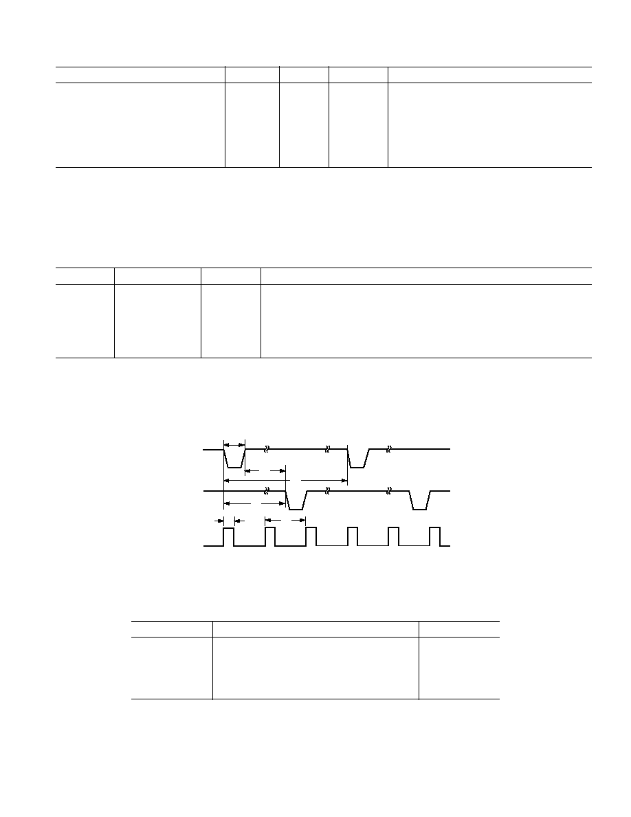
TIMING CHARACTERISTICS
1, 2
Parameter
A, B Versions
Unit
Test Conditions/Comments
t
1
3
275
ms
F1 and F2 Pulsewidth (Logic Low)
t
2
See Table III
sec
Output Pulse Period. See Transfer Function Section
t
3
1/2 t
2
sec
Time Between F1 Falling Edge and F2 Falling Edge
t
4
3, 4
90
ms
CF Pulsewidth (Logic High)
t
5
See Table IV
sec
CF Pulse Period. See Transfer Function Section
t
6
CLKIN/4
sec
Minimum Time Between F1 and F2 Pulse
NOTES
1
Sample tested during initial release and after any redesign or process change that may affect this parameter.
2
See Figure 1.
3
The pulsewidths of F1, F2 and CF are not fixed for higher output frequencies. See Frequency Outputs Section.
4
The CF pulse is always 18
µs in the high frequency mode. See Frequency Outputs section and Table IV.
Specifications subject to change without notice.
ORDERING GUIDE
Model
Package Description
Package Options
AD7755AAN
Plastic DIP
N-24
AD7755AARS
Shrink Small Outline Package
RS-24
AD7755ABRS
Shrink Small Outline Package
RS-24
EVAL-AD7755EB
AD7755 Evaluation Board
AD7755AAN-REF AD7755 Reference Design PCB (See AN-559)
(AV
DD
= DV
DD
= 5 V 5%, AGND = DGND = 0 V, On-Chip Reference, CLKIN = 3.58 MHz, T
MIN
to
T
MAX
= 40 C to +85 C)
.
t
2
.
t
3
t
4
.
t
5
.
t
6
t
1
F1
F2
CF
Figure 1. Timing Diagram for Frequency Outputs

REV. B
AD7755
4
ABSOLUTE MAXIMUM RATINGS
*
(T
A
= +25
°C unless otherwise noted)
AV
DD
to AGND . . . . . . . . . . . . . . . . . . . . . . . 0.3 V to +7 V
DV
DD
to DGND . . . . . . . . . . . . . . . . . . . . . . . 0.3 V to +7 V
DV
DD
to AV
DD
. . . . . . . . . . . . . . . . . . . . . . 0.3 V to +0.3 V
Analog Input Voltage to AGND
V1P, V1N, V2P and V2N . . . . . . . . . . . . . . . 6 V to +6 V
Reference Input Voltage to AGND . . 0.3 V to AV
DD
+ 0.3 V
Digital Input Voltage to DGND . . . 0.3 V to DV
DD
+ 0.3 V
Digital Output Voltage to DGND . . 0.3 V to DV
DD
+ 0.3 V
Operating Temperature Range
Industrial (A, B Versions) . . . . . . . . . . . . . 40
°C to +85°C
Storage Temperature Range . . . . . . . . . . . . 65
°C to +150°C
Junction Temperature . . . . . . . . . . . . . . . . . . . . . . . . . 150
°C
CAUTION
ESD (electrostatic discharge) sensitive device. Electrostatic charges as high as 4000 V readily
accumulate on the human body and test equipment and can discharge without detection.
Although the AD7755 features proprietary ESD protection circuitry, permanent damage may
occur on devices subjected to high-energy electrostatic discharges. Therefore, proper ESD
precautions are recommended to avoid performance degradation or loss of functionality.
WARNING!
ESD SENSITIVE DEVICE
24-Lead Plastic DIP, Power Dissipation . . . . . . . . . . 450 mW
JA
Thermal Impedance . . . . . . . . . . . . . . . . . . . . 105
°C/W
Lead Temperature, (Soldering 10 sec) . . . . . . . . . . . . 260
°C
24-Lead SSOP, Power Dissipation . . . . . . . . . . . . . . 450 mW
JA
Thermal Impedance . . . . . . . . . . . . . . . . . . . . 112
°C/W
Lead Temperature, Soldering
Vapor Phase (60 sec) . . . . . . . . . . . . . . . . . . . . . . 215
°C
Infrared (15 sec) . . . . . . . . . . . . . . . . . . . . . . . . . . . 220
°C
*Stresses above those listed under Absolute Maximum Ratings may cause perma-
nent damage to the device. This is a stress rating only; functional operation of the
device at these or any other conditions above those listed in the operational
sections of this specification is not implied. Exposure to absolute maximum rating
conditions for extended periods may affect device reliability.
TERMINOLOGY
MEASUREMENT ERROR
The error associated with the energy measurement made by the
AD7755 is defined by the following formula:
Percentage Error
True Energy
=
×
Energy Registered by the AD7755 True Energy
100%
PHASE ERROR BETWEEN CHANNELS
The HPF (High Pass Filter) in Channel 1 has a phase lead
response. To offset this phase response and equalize the phase
response between channels, a phase correction network is also
placed in Channel 1. The phase correction network matches the
phase to within
±0.1° over a range of 45 Hz to 65 Hz and ±0.2°
over a range 40 Hz to 1 kHz. See Figures 22 and 23.
POWER SUPPLY REJECTION
This quantifies the AD7755 measurement error as a percentage
of reading when the power supplies are varied.
For the ac PSR measurement a reading at nominal supplies
(5 V) is taken. A 200 mV rms/100 Hz signal is then introduced
onto the supplies and a second reading obtained under the same
input signal levels. Any error introduced is expressed as a per-
centage of reading--see Measurement Error definition.
For the dc PSR measurement a reading at nominal supplies
(5 V) is taken. The supplies are then varied
±5% and a second
reading is obtained with the same input signal levels. Any error
introduced is again expressed as a percentage of reading.
ADC OFFSET ERROR
This refers to the dc offset associated with the analog inputs to
the ADCs. It means that with the analog inputs connected to
AGND, the ADCs still see a small dc signal (offset). The offset
decreases with increasing gain in channel V1. This specification
is measured at a gain of 1. At a gain of 16, the dc offset is typi-
cally less than 1 mV. However, when the HPF is switched on,
the offset is removed from the current channel and the power
calculation is not affected by this offset.
GAIN ERROR
The gain error of the AD7755 is defined as the difference between
the measured output frequency (minus the offset) and the ideal
output frequency. It is measured with a gain of 1 in channel V1.
The difference is expressed as a percentage of the ideal frequency.
The ideal frequency is obtained from the AD7755 transfer func-
tion--see Transfer Function section.
GAIN ERROR MATCH
The gain error match is defined as the gain error (minus the
offset) obtained when switching between a gain of 1 and a
gain of 2, 8, or 16. It is expressed as a percentage of the out-
put frequency obtained under a gain of 1. This gives the gain
error observed when the gain selection is changed from 1 to 2,
8 or 16.

REV. B
AD7755
5
PIN FUNCTION DESCRIPTIONS
Pin No.
Mnemonic
Description
1
DV
DD
Digital Power Supply. This pin provides the supply voltage for the digital circuitry in the AD7755.
The supply voltage should be maintained at 5 V
± 5% for specified operation. This pin should be
decoupled with a 10
µF capacitor in parallel with a ceramic 100 nF capacitor.
2
AC/
DC
High Pass Filter Select. This logic input is used to enable the HPF in Channel 1 (the current channel).
A logic one on this pin enables the HPF. The associated phase response of this filter has been inter-
nally compensated over a frequency range of 45 Hz to 1 kHz. The HPF filter should be enabled in
power metering applications.
3
AV
DD
Analog Power Supply. This pin provides the supply voltage for the analog circuitry in the AD7755.
The supply should be maintained at 5 V
± 5% for specified operation. Every effort should be made to
minimize power supply ripple and noise at this pin by the use of proper decoupling. This pin should
be decoupled to AGND with a 10
µF capacitor in parallel with a ceramic 100 nF capacitor.
4, 19
NC
No Connect.
5, 6
V1P, V1N
Analog Inputs for Channel 1 (Current Channel). These inputs are fully differential voltage inputs with
a maximum differential signal level of
±470 mV for specified operation. Channel 1 also has a PGA and
the gain selections are outlined in Table I. The maximum signal level at these pins is
±1 V with respect
to AGND. Both inputs have internal ESD protection circuitry and in addition an overvoltage of
±6 V
can be sustained on these inputs without risk of permanent damage.
7, 8
V2N, V2P
Negative and Positive Inputs for Channel 2 (Voltage Channel). These inputs provide a fully differential
input pair. The maximum differential input voltage is
±660 mV for specified operation. The maximum
signal level at these pins is
± 1 V with respect to AGND. Both inputs have internal ESD protection
circuitry and an overvoltage of
±6 V can also be sustained on these inputs without risk of permanent
damage.
9
RESET
Reset Pin for the AD7755. A logic low on this pin will hold the ADCs and digital circuitry in a reset
condition. Bringing this pin logic low will clear the AD7755 internal registers.
10
REF
IN/OUT
This pin provides access to the on-chip voltage reference. The on-chip reference has a nominal value
of 2.5 V
± 8% and a typical temperature coefficient of 30 ppm/°C. An external reference source may
also be connected at this pin. In either case this pin should be decoupled to AGND with a 1
µF
ceramic capacitor and 100 nF ceramic capacitor.
11
AGND
This provides the ground reference for the analog circuitry in the AD7755, i.e., ADCs and reference.
This pin should be tied to the analog ground plane of the PCB. The analog ground plane is the ground
reference for all analog circuitry, e.g., antialiasing filters, current and voltage transducers, etc. For
good noise suppression the analog ground plane should only connected to the digital ground plane at
one point. A star ground configuration will help to keep noisy digital currents away from the analog
circuits.
12
SCF
Select Calibration Frequency. This logic input is used to select the frequency on the calibration output
CF. Table IV shows how the calibration frequencies are selected.
13, 14
S1, S0
These logic inputs are used to select one of four possible frequencies for the digital-to-frequency con-
version. This offers the designer greater flexibility when designing the energy meter. See Selecting a
Frequency for an Energy Meter Application section.
15, 16
G1, G0
These logic inputs are used to select one of four possible gains for Channel 1, i.e., V1. The possible
gains are 1, 2, 8 and 16. See Analog Input section.
17
CLKIN
An external clock can be provided at this logic input. Alternatively, a parallel resonant AT crystal can
be connected across CLKIN and CLKOUT to provide a clock source for the AD7755. The clock
frequency for specified operation is 3.579545 MHz. Crystal load capacitance of between 22 pF and
33 pF (ceramic) should be used with the gate oscillator circuit.
18
CLKOUT
A crystal can be connected across this pin and CLKIN as described above to provide a clock source
for the AD7755. The CLKOUT pin can drive one CMOS load when an external clock is supplied at
CLKIN or by the gate oscillator circuit.
20
REVP
This logic output will go logic high when negative power is detected, i.e., when the phase angle between
the voltage and current signals is greater that 90
°. This output is not latched and will be reset when
positive power is once again detected. The output will go high or low at the same time as a pulse is
issued on CF.