Äîêóìåíòàöèÿ è îïèñàíèÿ www.docs.chipfind.ru
24-Bit, 625 kSPS, 109 dB
- ADC
with On-Chip Buffers, Serial Interface
AD7763
Rev. 0
Information furnished by Analog Devices is believed to be accurate and reliable. However, no
responsibility is assumed by Analog Devices for its use, nor for any infringements of patents or other
rights of third parties that may result from its use. Specifications subject to change without notice. No
license is granted by implication or otherwise under any patent or patent rights of Analog Devices.
Trademarks and registered trademarks are the property of their respective owners.
One Technology Way, P.O. Box 9106, Norwood, MA 02062-9106, U.S.A.
Tel: 781.329.4700
www.analog.com
Fax: 781.461.3113
© 2005 Analog Devices, Inc. All rights reserved.
FEATURES
120 dB dynamic range at 78 kHz output data rate
109 dB dynamic range at 625 kHz output data rate
112 dB SNR at 78 kHz output data rate
107 dB SNR at 625 kHz output data rate
625 kHz maximum fully filtered output word rate
Programmable oversampling rate (32× to 256×)
Flexible serial interface
Fully differential modulator input
On-chip differential amplifier for signal buffering
Low-pass finite impulse response (FIR) filter with default
or user-programmable coefficients
Overrange alert bit
Digital offset and gain correction registers
Low power and power-down modes
Synchronization of multiple devices via SYNC pin
I
2
S interface mode
APPLICATIONS
Data acquisition systems
Vibration analysis
Instrumentation
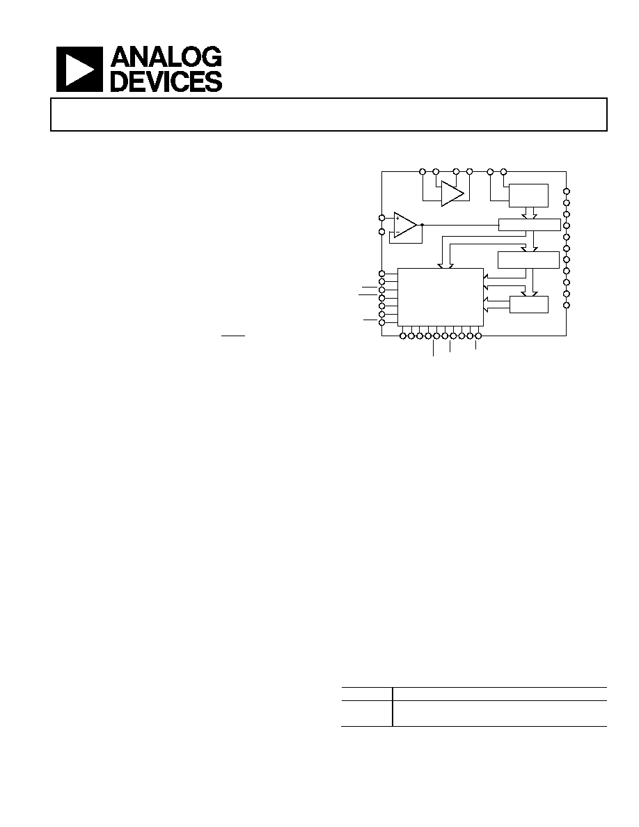
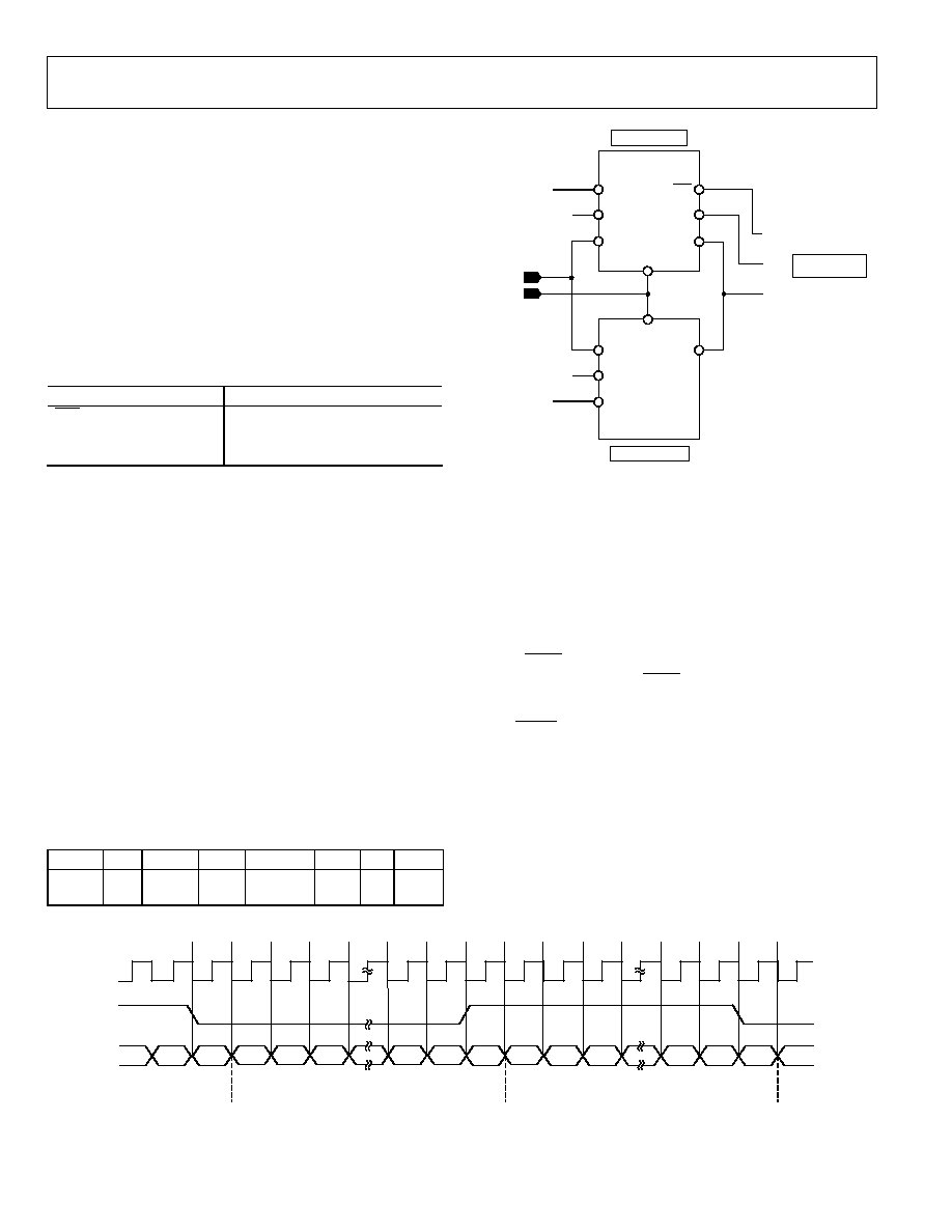
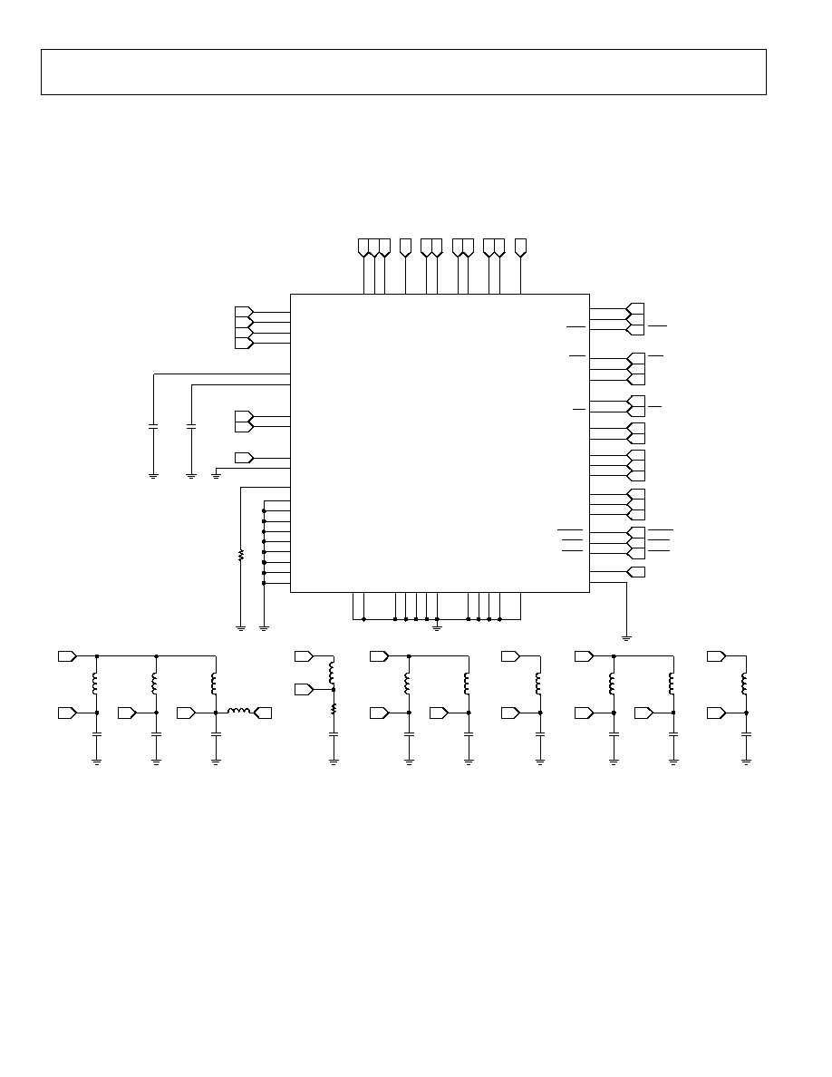
FUNCTIONAL BLOCK DIAGRAM
05476-
001
AD7763
V
IN+
V
IN
AV
DD1
AGND
MCLK
DGND
V
DRIVE
AV
DD2
AV
DD3
AV
DD4
DV
DD
DECAPA
R
BIAS
DECAPB
MCLKGND
SYNC
RESET
SH2:0
ADR2:0
CDIV
I
2
S
SCP
SC
R
SDL
DRD
Y
SC
O
FS
O
SD
O
SDI
FS
I
CONTROL LOGIC
I/O
OFFSET AND GAIN
REGISTERS
DIFF
MULTIBIT
-
MODULATOR
RECONSTRUCTION
V
REF+
REFGND
FIR FILTER
ENGINE
PROGRAMMABLE
DECIMATION
BUF
Figure 1.
GENERAL DESCRIPTION
The AD7763 high performance, 24-bit, - analog-to-digital
converter (ADC) combines wide input bandwidth and high
speed with the benefits of - conversion, as well as performance
of 107 dB SNR at 625 kSPS, making it ideal for high speed data
acquisition. A wide dynamic range, combined with significantly
reduced antialiasing requirements, simplifies the design process.
An integrated buffer to drive the reference, a differential ampli-
fier for signal buffering and level shifting, an overrange flag,
internal gain and offset registers, and a low-pass, digital FIR
filter make the AD7763 a compact, highly integrated data
acquisition device requiring minimal peripheral component
selection. In addition, the device offers programmable
decimation rates and a digital FIR filter, which can be user-
programmed to ensure that its characteristics are tailored for the
user's application. The AD7763 is ideal for applications demanding
high SNR without necessitating the design of complex, front-
end signal processing.
The differential input is sampled at up to 40 MSPS by an analog
modulator. The modulator output is processed by a series
of low-pass filters, the final filter having default or user-
programmable coefficients. The sample rate, filter corner
frequencies, and output word rate are set by a combination of
the external clock frequency and the configuration registers of
the AD7763.
The reference voltage supplied to the AD7763 determines the
analog input range. With a 4 V reference, the analog input range
is ±3.2 V differential-biased around a common mode of 2 V.
This common-mode biasing can be achieved using the on-chip
differential amplifiers, further reducing the external signal
conditioning requirements.
The AD7763 is available in an exposed paddle, 64-lead TQFP_EP
and is specified over the industrial temperature range from
-40°C to +85°C.
Table 1. Related Devices
Part No.
Description
AD7760
24-bit, 2.5 MSPS, 100 dB -, parallel interface
AD7762
24-bit, 625 kSPS, 109 dB -, parallel interface

AD7763
Rev. 0 | Page 2 of 32
TABLE OF CONTENTS
Features .............................................................................................. 1
Applications....................................................................................... 1
Functional Block Diagram .............................................................. 1
General Description ......................................................................... 1
Specifications..................................................................................... 3
Timing Specifications....................................................................... 5
Timing Diagrams.......................................................................... 6
Absolute Maximum Ratings............................................................ 7
ESD Caution.................................................................................. 7
Pin Configuration and Function Descriptions............................. 8
Terminology .................................................................................... 10
Typical Performance Characteristics ........................................... 11
Theory of Operation ...................................................................... 14
AD7763 Interface............................................................................ 15
Reading Data Using the SPI Interface ..................................... 15
Synchronization.......................................................................... 15
Sharing the Serial Bus ................................................................ 15
Writing to the AD7763 .............................................................. 16
Reading Status and Other Registers......................................... 17
Reading Data Using the I
2
S Interface....................................... 18
Clocking the AD7763..................................................................... 19
Example 1 .................................................................................... 19
Example 2 .................................................................................... 19
Driving the AD7763....................................................................... 20
Using the AD7763 ...................................................................... 21
Bias Resistor Selection ............................................................... 21
Decoupling and Layout Recommendations................................ 22
Supply Decoupling ..................................................................... 23
Additional Decoupling .............................................................. 23
Reference Voltage Filtering ....................................................... 23
Differential Amplifier Components ........................................ 23
Exposed Paddle........................................................................... 23
Layout Considerations............................................................... 23
Programmable FIR Filter............................................................... 24
Downloading a User-Defined Filter ............................................ 25
Example Filter Download ......................................................... 26
Registers........................................................................................... 27
Control Register 1--Address 0x001......................................... 27
Control Register 2--Address 0x002......................................... 27
Status Register (Read Only) ...................................................... 28
Offset Register--Address 0x003............................................... 28
Gain Register--Address 0x004 ................................................. 28
Overrange Register--Address 0x005....................................... 28
Outline Dimensions ....................................................................... 29
Ordering Guide .......................................................................... 29
REVISION HISTORY
10/05--Revision 0: Initial Version

AD7763
Rev. 0 | Page 3 of 32
SPECIFICATIONS
AV
DD1
= DV
DD
= V
DRIVE
= 2.5 V; AV
DD2
= AV
DD3
= AV
DD4
= 5 V; V
REF
= 4.096 V; MCLK amplitude = 5 V; T
A
= 25°C; normal mode,
using on-chip amplifier with components as shown in Table 10, unless otherwise noted.
1
Table 2.
Parameter Test
Conditions/Comments
Specification
Unit
DYNAMIC PERFORMANCE
Decimate × 256
MCLK = 40 MHz, ODR = 78 kHz, F
IN
= 1 kHz
Dynamic Range
Modulator inputs shorted
119
120.5
dB min
dB typ
Signal-to-Noise Ratio (SNR)
2
Input amplitude = -0.5 dBFS
112
dB typ
Input amplitude = -60 dB
59
dBc typ
Nonharmonic, input amplitude = -6 dB
126
dBc typ
Spurious-Free Dynamic Range (SFDR)
Input amplitude = -60 dB
77
dBc typ
Input amplitude = -0.5 dBFS
-105
dB typ
Input amplitude = -6 dB
-106
dBc typ
Total Harmonic Distortion (THD)
Input amplitude = -60 dB
-75
dBc typ
Decimate × 64
MCLK = 40 MHz, ODR = 312.5 kHz, F
IN
= 1 kHz
Dynamic Range
Modulator inputs shorted
112
113
dB min
dB typ
Signal-to-Noise Ratio (SNR)
2
Input amplitude = -0.5 dBFS
109.5
dB typ
Spurious-Free Dynamic Range (SFDR)
Nonharmonic, input amplitude = -6 dB
126
dBc typ
Decimate × 32
MCLK = 40 MHz, ODR = 625 kHz, F
IN
= 100 kHz
Dynamic Range
Modulator inputs shorted
108
109.5
dB min
dB typ
Signal-to-Noise Ratio (SNR)
2
Input amplitude = -0.5 dBFS
107
dB typ
Nonharmonic, input amplitude = -6 dB
120
dBc typ
Input amplitude = -0.5 dBFS
-105
dB typ
Spurious-Free Dynamic Range (SFDR)
Total Harmonic Distortion (THD)
Input amplitude = -6 dB
-107
dBc typ
DC ACCURACY
Resolution
24
Bits
Differential Nonlinearity
Guaranteed monotonic to 24 bits
Integral Nonlinearity
0.00076
% typ
0.014 %
typ
Zero Error
0.02 %
max
Gain Error
0.018
% typ
Zero Error Drift
10
%FS/°C typ
Gain Error Drift
0.0002
%FS/°C typ
DIGITAL FILTER RESPONSE
Decimate × 32
Group Delay
MCLK = 40 MHz
47
s typ
Decimate × 64
Group Delay
MCLK = 40 MHz
91.5
s typ
Decimate × 256
Group Delay
MCLK = 40 MHz
358
s typ
ANALOG INPUT
Differential Input Voltage
V
IN
(+) V
IN
(-), V
REF
= 2.5 V
±2
V p-p
V
IN
(+) V
in
(-), V
REF
= 4.096 V
±3.25
V p-p
Input Capacitance
At internal buffer inputs
5
pF typ
At modulator inputs
55
pF typ

AD7763
Rev. 0 | Page 4 of 32
Parameter Test
Conditions/Comments
Specification
Unit
REFERENCE INPUT
V
REF
Input Voltage
V
DD3
= 3.3 V ± 5%
+2.5
V max
V
DD3
= 5 V ± 5%
+4.096
V max
V
REF
Input DC Leakage Current
±1
A max
V
REF
Input Capacitance
5
pF max
POWER DISSIPATION
Total Power Dissipation
Normal power mode
955.5
mW max
Low power mode
651
mW max
Standby Mode
Clock stopped
6.35
mW typ
POWER REQUIREMENTS
AV
DD1
(Modulator Supply)
±5%
+2.5
V
AV
DD2
(General Supply)
±5%
+5
V
AV
DD3
(Differential Amplifier Supply)
+3.15/+5.25
V min/max
AV
DD4
(Reference Buffer Supply)
+3.15/+5.25
V min/max
DV
DD
±5% +2.5
V
V
DRIVE
+1.65/+2.7
V
min/max
Normal Mode
AI
DD1
(Modulator)
49/52
mA typ/max
AI
DD2
(General)
40/43
mA typ/max
AI
DD4
(Reference Buffer)
AV
DD4
= 5 V
35/37
mA typ/max
Low Power Mode
AI
DD1
(Modulator)
26/28
mA typ/max
AI
DD2
(General)
20/23
mA typ/max
AI
DD4
(Reference Buffer)
AV
DD4
= 5 V
10/11
mA typ/max
AI
DD3
(Diff Amp)
AV
DD3
= 5 V, both modes
41/45
mA typ/max
DI
DD
Both modes
56/62
mA typ/max
DIGITAL I/O
MCLK Input Amplitude
3
5
V
typ
Input Capacitance
7.3
pF typ
Input Leakage Current
±1
A/pin max
Three-State Leakage Current (SDO)
±1
A max
V
INH
0.7
×
V
DRIVE
V min
V
INL
0.3
×
V
DRIVE
V max
V
OH
4
1.5
V
min
V
OL
0.1
V
max
1
See the Terminology section.
2
SNR specifications in dB are referred to a full-scale input, FS, and tested with an input signal at 0.5 dB below full scale, unless otherwise specified.
3
While the AD7763 can function with an MCLK amplitude of less than 5 V, this is the recommended amplitude to achieve the performance as stated.
4
Tested with a 400 A load current.
AD7763
Rev. 0 | Page 5 of 32
TIMING SPECIFICATIONS
AV
DD1
= DV
DD
= V
DRIVE
= 2.5 V, AV
DD2
= AV
DD3
= AV
DD4
= 5 V, T
A
= 25°C, normal mode, unless otherwise noted.
Table 3.
Parameter
Limit at T
MIN
, T
MAX
Unit
Description
f
MCLK
1
MHz min
Applied master clock frequency
40
MHz
max
f
ICLK
500
kHz min
Internal modulator clock derived from MCLK
20
MHz
max
t
1
1
1 × t
ICLK
or 0.5 × t
ICLK
2
typ
SCO high period
t
2
1
2
1 × t
ICLK
or 0.5 × t
ICLK
typ
SCO low period
t
3
t
SCO
3
typ
DRDY low period
t
3A
4
2 ns
typ
SCO rising edge to DRDY falling edge
t
3B
4
3 ns
typ
SCO rising edge to DRDY rising edge
t
4
5
32 × t
SCO
3
typ
FSO low period
t
4A
4, 5
1 ns
typ
SCO rising edge to FSO falling edge
t
4B
4, 5
2 ns
typ
SCO falling edge to FSO rising edge
t
5
6.5
ns max
Initial data access time
t
6
4
5
ns max
SCO rising edge to SDO valid
t
7
0.5 × t
SCO
3
ns min
SDO valid after SCO falling edge
t
8
16 × t
SCO
3
typ
DRDY rising edge to SDL falling edge
t
9
t
SCO
3
typ
SDL pulse width
t
10
5.5
ns max
SDO three-state to SCO rising edge
t
11
1 × t
SCO
3
min
FSI low period
t
12
12
ns min
SDI setup time
t
13
10
ns min
SDI hold time
t
14
12 ns
min
FSI setup time
t
15
16 × t
SCO
3
typ
SDL falling edge to SDL falling edge
1
t
ICLK
= 1/f
ICLK
.
2
SCO frequency selected by SCR and CDIV pins.
3
t
SCO
= t
1
+ t
2
.
4
All edges mentioned refer to SCP = 0. Invert SCO edges for SCP = 1.
5
In decimate × 32 mode, this time specification applies only when CDIV = 0 and SCR =1. For all other combinations of CDIV and SCR in decimate × 32 mode, the FSO
signal is constantly logic low.
AD7763
Rev. 0 | Page 6 of 32
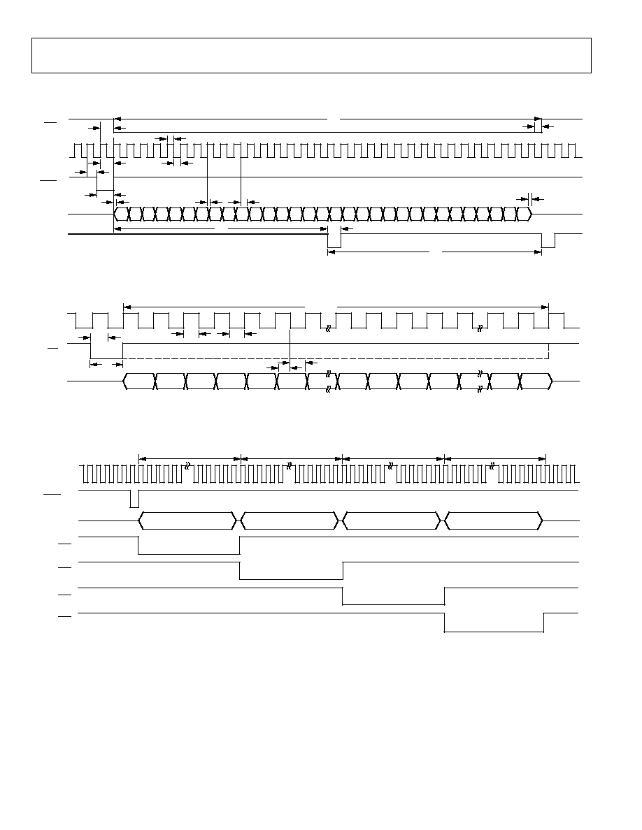
TIMING DIAGRAMS
D23 D22 D21 D20 D19 D18 D17 D16 D15 D14 D13 D12 D11 D10 D9
D8
D7
D6
D5
D4
D3
D2
D1
D0 ST6 ST5 ST4 ST3 ST2 ST1 ST0
FSO (O)
SCO (O)
DRDY (O)
SDO (O)
SDL (O)
t
10
t
4B
t
4A
t
3
t
3B
t
3A
t
2
t
5
t
6
t
7
t
9
t
1
t
4
t
8
t
15
05
47
6-
0
02
Figure 2. SPI® Interface Serial Read Timing Diagram
ALL
ADR2
ADR1
ADR0
RA11
RA10
RA1
RA0
D15
D14
D1
D0
SCO (O)
FSI (I)
SDI (I)
32 ×
t
SCO
t
1
t
14
t
12
t
13
t
2
t
11
05
47
6-
00
3
Figure 3. Register Write
SERIAL DATA FROM ADC A
32 ×
t
SCO
SERIAL DATA FROM ADC B
SERIAL DATA FROM ADC C
SERIAL DATA FROM ADC D
FSO B
DRDY A (O)
SCO (O)
SDO (O)
FSO C
FSO D
FSO A
32 ×
t
SCO
32 ×
t
SCO
32 ×
t
SCO
05
47
6-
0
04
Figure 4. SPI Interface Serial Read Timing with Multiple AD7763 Devices Sharing the Serial Bus
AD7763
Rev. 0 | Page 7 of 32
ABSOLUTE MAXIMUM RATINGS
T
A
= 25°C, unless otherwise noted.
Table 4.
Parameter Rating
AV
DD1
to GND
-0.3 V to +3 V
(AV
DD2
, AV
DD3
, AV
DD4
) to GND
-0.3 V to +6 V
DV
DD
to GND
-0.3 V to +3 V
V
DRIVE
to GND
-0.3 V to +3 V
V
IN+
, V
IN
to GND
-0.3 V to +6 V
Digital Input Voltage to GND
1
-0.3 V to DV
DD
+ 0.3 V
MCLK to MCLKGND
-0.3 V to +6 V
V
REF
to GND
2
-0.3 V to AV
DD4
+ 0.3 V
AGND to DGND
-0.3 V to +0.3 V
Input Current to Any Pin
Except Supplies
3
±10 mA
Operating Temperature Range
Commercial
-40°C to +85°C
Storage Temperature Range
-65°C to +150°C
Junction Temperature
150°C
TQFP_EP Exposed Paddle
JA
Thermal Impedance
92.7°C/W
JC
Thermal Impedance
5.1°C/W
Lead Temperature, Soldering
Vapor Phase (60 sec)
215°C
Infrared (15 sec)
220°C
ESD 600
V
1
Absolute maximum voltage on digital inputs is 3.0 V or DV
DD
+ 0.3 V,
whichever is lower.
2
Absolute maximum voltage on V
REF
input is 6.0 V or AV
DD4
+ 0.3 V,
whichever is lower.
3
Transient currents of up to 200 mA do not cause SCR latch-up.
Stresses above those listed under Absolute Maximum Ratings
may cause permanent damage to the device. This is a stress
rating only; functional operation of the device at these or any
other conditions above those indicated in the operational
section of this specification is not implied. Exposure to absolute
maximum rating conditions for extended periods may affect
device reliability.
ESD CAUTION
ESD (electrostatic discharge) sensitive device. Electrostatic charges as high as 4000 V readily accumulate on the
human body and test equipment and can discharge without detection. Although this product features
proprietary ESD protection circuitry, permanent damage may occur on devices subjected to high energy
electrostatic discharges. Therefore, proper ESD precautions are recommended to avoid performance
degradation or loss of functionality.
AD7763
Rev. 0 | Page 8 of 32
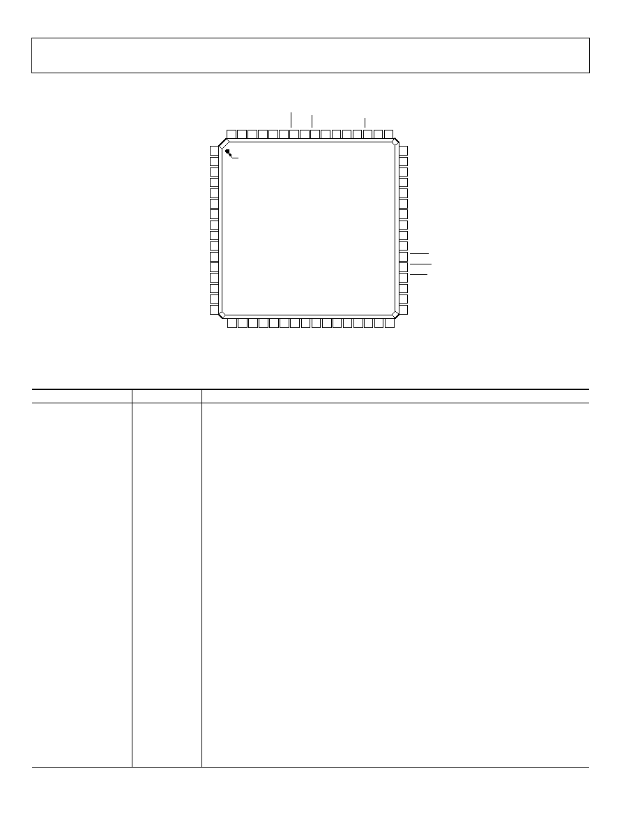
PIN CONFIGURATION AND FUNCTION DESCRIPTIONS
64
DG
ND
63
V
DR
I
V
E
62
DG
ND
61
I
2
S
60
SC
R
59
DG
ND
58
CD
I
V
57
DG
ND
56
FS
O
55
SC
O
54
SD
O
53
DG
ND
52
SD
I
51
FS
I
50
SDL
49
SCP
47
ADR1
46
ADR2
45
SH0
42
DGND
43
DGND
44
V
DRIVE
48
ADR0
41
DV
DD
40
SH1
39
SH2
37
RESET
36
SYNC
35
DGND
34
AGND1
33
AV
DD1
38
DRDY
2
MCLKGND
3
MCLK
4
AV
DD2
7
AGND1
6
AV
DD1
5
AGND2
1
DGND
8
DECAPA
9
REFGND
10
V
REF+
12
AV
DD4
13
AGND2
14
AV
DD2
15
AV
DD2
16
AGND2
11
AGND4
PIN 1
17
R
BI
A
S
18
AG
ND2
19
V
IN
A+
20
V
IN
A
21
V
OU
T
A
22
V
OU
T
A+
23
AG
ND3
24
AV
DD
3
25
V
IN
+
26
V
IN
27
AV
DD
2
28
AG
ND2
29
AG
ND3
30
DE
CAP
B
31
AG
ND3
32
AG
ND3
AD7763
TOP VIEW
(Not to Scale)
05
47
6-
00
5
Figure 5. Pin Configuration
Table 5. Pin Function Descriptions
Pin No.
Mnemonic
Description
6, 33
AV
DD1
Power Supply for Modulator, 2.5 V. These pins should be decoupled to AGND1 with 100 nF and
10 F capacitors on each pin.
4, 14, 15, 27
AV
DD2
Power Supply, 5 V. These pins should be decoupled to AGND2 with 100 nF capacitors on each of
Pin 4, Pin 14, and Pin 15. Pin 27 should be connected to Pin 14 via an 8.2 nH inductor.
24 AV
DD3
Power Supply for Differential Amplifier, 3.3 V to 5 V. This pin should be decoupled to AGND3
with a 100 nF capacitor.
12 AV
DD4
Power Supply for Reference Buffer, 3.3 V to 5 V. This pin should be decoupled to AGND4
with a 10 nF capacitor in series with a 10
resistor.
7, 34
AGND1
Power Supply Ground for Analog Circuitry Powered by AV
DD1
.
5, 13, 16, 18, 28
AGND2
Power Supply Ground for Analog Circuitry Powered by AV
DD2
.
23, 29, 31, 32
AGND3
Power Supply Ground for Analog Circuitry Powered by AV
DD3
.
11
AGND4
Power Supply Ground for Analog Circuitry Powered by AV
DD4
.
9
REFGND
Reference Ground. Ground connection for the reference voltage.
41 DV
DD
Power Supply for Digital Circuitry and FIR Filter, 2.5 V. This pin should be decoupled to DGND
with a 100 nF capacitor.
44, 63
V
DRIVE
Logic Power Supply Input, 1.8 V to 2.5 V. The voltage supplied at these pins determines
the operating voltage of the logic interface. These pins must be connected together and
tied to the same supply. Each pin should also be decoupled to DGND with a 100 nF capacitor.
1, 35, 42, 43, 53, 57, 59,
62, 64
DGND
Ground Reference for Digital Circuitry.
19 V
IN
A+
Positive Input to Differential Amplifier.
20 V
IN
A-
Negative Input to Differential Amplifier.
21 V
OUT
A-
Negative Output from Differential Amplifier.
22 V
OUT
A+ Positive
Output
from
Differential Amplifier.
25 V
IN
+
Positive Input to the Modulator.
26 V
IN
-
Negative Input to the Modulator.
10 V
REF+
Reference Input. The input range of this pin is determined by the reference buffer
supply voltage (AV
DD4
). See the Reference Voltage Filtering section for more details.
8
DECAPA
Decoupling Pin. A 100 nF capacitor must be inserted between this pin and AGND1.
30
DECAPB
Decoupling Pin. A 33 pF capacitor must be inserted between this pin and AGND3.
AD7763
Rev. 0 | Page 9 of 32
Pin No.
Mnemonic
Description
17 R
BIAS
Bias Current Setting. A resistor must be inserted between this pin and AGND.
See the Bias Resistor Selection section.
37
RESET
A falling edge on this pin resets all internal digital circuitry. Holding this pin low
keeps the AD7763 in a reset state.
3 MCLK
Master Clock Input. A low jitter digital clock must be applied to this pin. The output data rate
depends on the frequency of this clock. See the Clocking the AD7763 section.
2
MCLKGND
Master Clock Ground Sensing Pin.
36
SYNC
Synchronization Input. A falling edge on this pin resets the internal filter. This can be used
to synchronize multiple devices in a system.
38
DRDY
Data Ready Output. Each time new conversion data is available, an active low pulse,
½ ICLK period wide, is produced on this pin. See the AD7763 Interface section.
39, 40, 45
SH2:0
Share Pins 2:0. For multiple AD7763 devices sharing a common serial bus. Each device is wired
with the binary value that represents the number of devices sharing the serial bus. SH2 is the
MSB. See the Sharing the Serial Bus section.
46 to 48
ADR2:0
Address 2:0. Allows multiple AD7763 devices to share a common serial bus. Each device must be
programmed with an individual address using these three pins. See the Sharing the Serial Bus
section.
49 SCP
Serial Clock Polarity. Determines on which edge of SCO the data bits are clocked out and on
which edge they are valid. All timing diagrams are shown with SCP = 0, and all SCO edges
shown should be inverted for SCP = 1.
50 SDL
Serial Data Latch. A pulse is output on this pin after every 16 data bits. The pulse is one SCO
period wide and can be used in conjunction with FSO as an alternative framing method for
serial transfers requiring a framing signal more frequent than every 32 bits.
51
FSI
Frame Sync In. The status of this pin is checked on the falling edge of SCO. If this pin is low, then
the first data bit is latched in on the next SCO falling edge when SCP = 0 or on the rising edge of
SCO if SCP = 1.
52 SDI
Serial Data In. The first data bit (MSB) must be valid on the next SCO falling edge when SCP = 0
(or SCO rising edge SCP = 1) after the FSI event has been latched. Each write requires 32 bits: the
ALL bit, 3 address bits, and 12 register address bits, followed by the remaining 16 bits of data to
be written to the device.
54 SDO
Serial Data Out. Address, status, and data bits are clocked out on this line during each serial
transfer.
If SCP = 0, each bit is clocked out on an SCO rising edge and is valid on the falling edge. When
the I
2
S pin is set to logic high, this pin outputs the signal defined as SD in the I
2
S bus
specification. See the Reading Data Using the I S Interface
2
section for details.
55 SCO
Serial Clock Out. This clock signal is derived from the internal ICLK signal. The frequency of SCO
is equal to either ICLK or ICLK/2, depending on the state of the CDIV and SCR pins (see the
AD7763 Interface section). When the I
2
S pin is logic high, this pin outputs the signal defined as
SCK by the I
2
S bus specification. See the Reading Data Using the I S Interface
2
section.
56
FSO
Frame Sync Out. This signal frames the serial data output and is 32 SCO periods wide. The
exception to the framing behavior of FSO occurs in decimate × 32 mode, where, for certain
combinations of CDIV and SCR, the FSO signal is constantly logic low. See the Reading Data
Using the SPI Interface section. When the I
2
S pin is set to logic high, this pin outputs the signal
defined as WS in the I
2
S bus specification. See the Reading Data Using the I S Interface
2
section.
58
CDIV
Clock Divider. This pin is used to select the ratio of MCLK to ICLK. See the AD7763 Interface
section.
60 SCR
Serial Clock Rate. This pin and the CDIV pin program the SCO frequency (see Table 7).
61 I
2
S
I
2
S Select. A Logic 1 on this pin changes the serial data-out mode from SPI to I
2
S. The SDO pin
outputs as the SD signal, the SCO pin outputs the SCK signal, and the FSO pin outputs the WS
signal. When writing to the AD7763, the I
2
S pin is set to logic low and the SPI interface is used.
See the Reading Data Using the I S Interface
2
section for further details.

AD7763
Rev. 0 | Page 10 of 32
TERMINOLOGY
Signal-to-Noise Ratio (SNR)
The ratio of the rms value of the actual input signal to the rms
sum of all other spectral components below the Nyquist fre-
quency, excluding harmonics and dc. The value for SNR is
expressed in decibels.
Total Harmonic Distortion (THD)
The ratio of the rms sum of harmonics to the fundamental. For
the AD7763, it is defined as
( )
1
6
5
4
3
2
V
V
V
V
V
V
THD
2
2
2
2
2
log
20
dB
+
+
+
+
=
where:
V
1
is the rms amplitude of the fundamental.
V
2
, V
3
, V
4
, V
5
, and V
6
are the rms amplitudes of the second
to the sixth harmonic.
Nonharmonic Spurious-Free Dynamic Range (SFDR)
The ratio of the rms signal amplitude to the rms value of the
peak spurious spectral component, excluding harmonics.
Dynamic Range
The ratio of the rms value of the full scale to the rms noise
measured with the inputs shorted together. The value for
dynamic range is expressed in decibels.
Integral Nonlinearity (INL)
The maximum deviation from a straight line passing through
the endpoints of the ADC transfer function.
Differential Nonlinearity (DNL)
The difference between the measured and the ideal 1 LSB
change between any two adjacent codes in the ADC.
Zero Error
The difference between the ideal midscale input voltage (0 V)
and the actual voltage producing the midscale output code.
Zero Error Drift
The change in the actual zero error value due to a temperature
change of 1°C. It is expressed as a percentage of full scale at room
temperature.
Gain Error
The first transition (from 100...000 to 100...001) should occur
for an analog voltage 1/2 LSB above the nominal negative full
scale. The last transition (from 011...110 to 011...111) should
occur for an analog voltage 1 1/2 LSB below the nominal full
scale. The gain error is the deviation of the difference between
the actual level of the last transition and the actual level of the
first transition, from the difference between the ideal levels.
Gain Error Drift
The change in the actual gain error value due to a temperature
change of 1°C. It is expressed as a percentage of full scale at
room temperature.
AD7763
Rev. 0 | Page 11 of 32
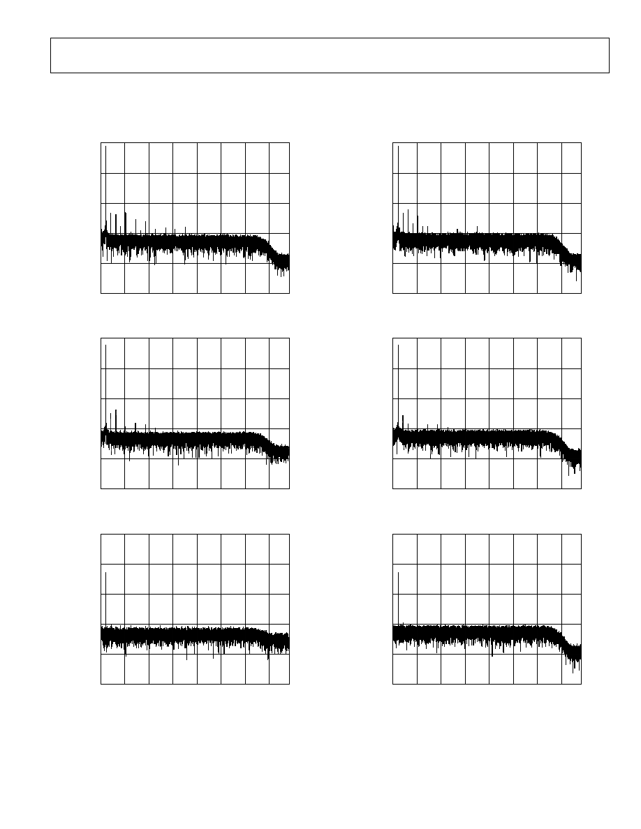
TYPICAL PERFORMANCE CHARACTERISTICS
AV
DD1
= DV
DD
= V
DRIVE
= 2.5 V, AV
DD2
= AV
DD3
= AV
DD4
= 5 V, V
REF
= 4.096 V, T
A
= 25°C, normal mode, unless otherwise noted. All FFTs
are generated from 65536 samples using a 7-term Blackman-Harris window.
0
50
100
150
200
250
0
5000
15000
10000
30000 35000
25000
20000
05
476
-
00
7
AM
P
L
I
T
UDE
(
d
B
)
FREQUENCY (Hz)
Figure 6. Normal Mode FFT, 1 kHz, -0.5 dB Input Tone, 256× Decimation
0
50
100
150
200
250
0
5000
15000
10000
30000 35000
25000
20000
05
47
6-
01
1
AM
P
L
I
T
UDE
(
d
B)
FREQUENCY (Hz)
Figure 7. Normal Mode FFT, 1 kHz, -0.6 dB Input Tone, 256× Decimation
0
50
100
150
200
250
0
5000
15000
10000
30000 35000
25000
20000
05
47
6-
03
2
AM
P
L
I
T
UDE
(
d
B)
FREQUENCY (Hz)
Figure 8. Normal Mode FFT, 1 kHz, -60 dB Input Tone, 256× Decimation
0
50
100
150
200
250
0
5000
15000
10000
30000 35000
25000
20000
05
476
-
00
6
AM
P
L
I
T
UDE
(
d
B
)
FREQUENCY (Hz)
Figure 9. Low Power FFT, 1 kHz, -0.5 dB Input Tone, 256× Decimation
0
50
100
150
200
250
0
5000
15000
10000
30000 35000
25000
20000
05
47
6-
01
0
AM
P
L
I
T
UDE
(
d
B)
FREQUENCY (Hz)
Figure 10. Low Power FFT, 1 kHz, -6 dB Input Tone, 256× Decimation
0
50
100
150
200
250
0
5000
15000
10000
30000 35000
25000
20000
05
47
6-
03
1
AM
P
L
I
T
UDE
(
d
B)
FREQUENCY (Hz)
Figure 11. Low Power FFT, 1 kHz, -60 dB Input Tone, 256× Decimation
AD7763
Rev. 0 | Page 12 of 32
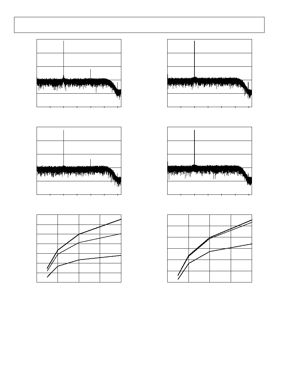
0
50
100
150
200
250
0
50000
150000
100000
300000
250000
200000
05
47
6-
00
9
AM
P
L
I
T
UDE
(
d
B)
FREQUENCY (Hz)
Figure 12. Normal Mode FFT, 100 kHz, -0.5 dB Input Tone, 32× Decimation
0
50
100
150
200
250
0
50000
150000
100000
300000
250000
200000
05
47
6-
03
0
AM
P
L
I
T
UDE
(
d
B)
FREQUENCY (Hz)
Figure 13. Normal Mode FFT, 100 kHz, -6 dB Input Tone, 32× Decimation
120
114
116
118
112
110
108
106
0
64
6dB
60dB
0.5dB
192
128
256
05
476
-
03
6
S
NR (
d
BF
S
)
DECIMATION RATE (
×
)
Figure 14. Normal Mode SNR vs. Decimation Rate, 1 kHz Input Tone
0
50
100
150
200
250
0
50000
150000
100000
300000
250000
200000
05
47
6-
00
8
AM
P
L
I
T
UDE
(
d
B)
FREQUENCY (Hz)
Figure 15. Low Power FFT, 100 kHz, -0.5 dB Input Tone, 32× Decimation
0
50
100
150
200
250
0
50000
150000
100000
300000
250000
200000
05
47
6-
02
9
AM
P
L
I
T
UDE
(
d
B)
FREQUENCY (Hz)
Figure 16. Low Power FFT, 100 kHz, -6 dB Input Tone, 32× Decimation
116
114
112
110
108
106
104
0
64
6dB
60dB
0.5dB
192
128
256
05
476
-
03
3
S
NR (
d
BF
S
)
DECIMATION RATE (
×
)
Figure 17. Low Power SNR vs. Decimation Rate, 1 kHz Input Tone
AD7763
Rev. 0 | Page 13 of 32
4500
1000
500
1500
2000
2500
3000
3500
4000
0
8385341
8385401
8385391
8385381
8385371
8385361
8385351
05
47
6-
03
5
O
CCURE
NCE
24-BIT CODE
Figure 18. Normal Mode, 24-Bit Histogram, 256× Decimation
0.0010
0.0010
0
16777216
05
47
6-
0
37
24-BIT CODE
IN
L
(
%
)
0.0005
0
0.0005
4194304
8388608
12582912
+25
°
C
40
°
C
+85
°
C
Figure 19. 24-Bit INL, Normal Power Mode
0.65
0.6
0
16777216
05
47
6-
0
39
24-BIT CODE
DN
L (
L
S
B
)
0.2
0.4
0
0.2
0.4
4194304
8388608
12582912
Figure 20. 24-Bit DNL
6000
1000
2000
3000
4000
5000
0
8383091
8383191
8383171
8383151
8383131
8383111
05
47
6-
03
4
O
CCURE
NCE
24-BIT CODE
Figure 21. Low Power 24-Bit Histogram, 256× Decimation
0.0015
0.0010
0
16777216
05
47
6-
0
38
24-BIT CODE
IN
L
(
%
)
0.0005
0.0010
0
0.0005
4194304
8388608
12582912
+25
°
C
40
°
C
+85
°
C
Figure 22. 24-Bit INL, Low Power Mode
AD7763
Rev. 0 | Page 14 of 32
THEORY OF OPERATION
The AD7763 employs a - conversion technique to convert
the analog input into an equivalent digital word. The modulator
samples the input waveform and outputs an equivalent digital
word to the digital filter at a rate equal to ICLK.
Due to the high oversampling rate, which spreads the quanti-
zation noise from 0 to f
ICLK
, the noise energy contained in the
band of interest is reduced (see Figure 23). To further reduce
quantization noise, a high order modulator is employed to shape
the noise spectrum; thus, most of the noise energy is shifted out
of the band of interest (see Figure 24).
The digital filtering that follows the modulator removes the
large out-of-band quantization noise (see Figure 25), while
also reducing the data rate from f
ICLK
at the input of the filter
to f
ICLK
/32 or less at the output of the filter, depending on the
decimation rate used.
Digital filtering has certain advantages over analog filtering.
It does not introduce significant noise or distortion and can
be made perfectly linear phase.
The AD7763 employs three finite impulse response (FIR) filters
in series. By using different combinations of decimation ratios
and filter selection, data can be obtained from the AD7763 at
four different data rates. The first filter receives data from the
modulator at ICLK
MHz,
where it is decimated × 4 to output
data at (ICLK/4)
MHz
.
The second filter allows the decimation rate to be chosen from
8× to 32×. The third filter has a fixed decimation rate of 2x, is
user programmable, and has a default configuration (see the
Programmable FIR Filter section). This filter can be bypassed.
Table 6 shows some characteristics of the default filter. The group
delay of the filter is defined as the delay to the center of the
impulse response and is equal to the computation plus filter
delays. The delay until valid data is available (the DVALID status bit
is set) is equal to 2× the filter delay plus the computation delay.
05
47
6-
0
2
4
QUANTIZATION NOISE
f
ICLK
/2
BAND OF INTEREST
Figure 23. - ADC, Quantization Noise
05
47
6-
02
5
f
ICLK
/2
NOISE SHAPING
BAND OF INTEREST
Figure 24. - ADC, Noise Shaping
05
47
6-
01
2
f
ICLK
/2
BAND OF INTEREST
DIGITAL FILTER CUTOFF FREQUENCY
Figure 25. - ADC, Digital Filter Cutoff Frequency
Table 6. Configuration With Default Filter
ICLK
Frequency
Filter
1
Filter
2
Filter 3
Data State
Computation
Delay
Filter
Delay
Pass Band
Bandwidth
Output Data Rate
(ODR)
20 MHz
4×
4×
2×
Fully filtered
1.775 s
44.4 s
250 kHz
625 kHz
20 MHz
4×
8×
Bypassed
Partially
filtered
2.6 s
10.8 s
140.625 kHz
625 kHz
20 MHz
4×
8×
2×
Fully filtered
2.25 s
87.6 s
125 kHz
312.5 kHz
20 MHz
4×
16×
Bypassed
Partially
filtered
4.175 s
20.4 s
70.3125 kHz
312.5 kHz
20 MHz
4×
16×
2×
Fully filtered
3.1 s
174 s
62.5 kHz
156.25 kHz
20 MHz
4×
32×
Bypassed
Partially
filtered
7.325 s
39.6 s
35.156 kHz
156.25 kHz
20 MHz
4×
32×
2×
Fully filtered
4.65 s
346.8 s
31.25 kHz
78.125 kHz
12.288 MHz
4×
8×
2×
Fully filtered
3.66 s
142.6 s
76.8 kHz
192 kHz
12.288 MHz
4×
16×
2×
Fully filtered
5.05 s
283.2 s
38.4 kHz
96 kHz
12.288 MHz
4×
32×
Bypassed
Partially
filtered
11.92 s
64.45 s
21.6 kHz
96 kHz
12.288 MHz
4×
32×
2×
Fully filtered
7.57 s
564.5 s
19.2 kHz
48 kHz
AD7763
Rev. 0 | Page 15 of 32
AD7763 INTERFACE
READING DATA USING THE SPI INTERFACE
The timing diagram in Figure 2 shows how the AD7763 transmits
its conversion results using the SPI-compatible serial interface.
The data being read from the AD7763 is clocked out using the
serial clock output, SCO. The SCO frequency is dependent on
the state of the serial clock output rate pin, SCR, and the clock
divider mode chosen by the state of the clock divider pin, CDIV
(see the Clocking the AD7763 section). Table 7 shows both the
SCO frequency and the ICLK frequency for the AD7763, resulting
from the states of both the CDIV and SCR pins.
Table 7. SCO Frequency
Clock Divide
Mode
CDIV
SCR
SCO
Frequency
ICLK
Frequency
Divide by 1
1
0
MCLK
MCLK
1
MCLK
MCLK
Divide by 2
0
0
MCLK/2
MCLK/2
1
MCLK
1
MCLK/2
1
In decimate × 32 mode, when CDIV = 0 and SCR = 1, FSO pulses low for
32 SCO clock cycles, as shown in Figure 2. For all other combinations of CDIV
and SCR in decimate × 32 mode, FSO is continuously low.
An active low pulse of one SCO period on the data-ready output,
DRDY, indicates a new conversion result is available at the
AD7763 serial data output, SDO.
Each bit of the new conversion result is clocked onto the SDO
line on the rising SCO edge and is valid on the falling SCO edge
(for SCP = 0). The conversion result spans 32 SCO clock cycles
and consists of 24 data bits in twos complement form, followed
by 7 status bits.
D6 D5 D4 D3 D2
D1 D0
ADR2 ADR1 ADR0 DVALID OVR LPWR FILTER_OK
The conversion result output on the SDO line is framed by the
frame synchronization output, FSO, which is sent logic low for
32 SCO cycles following the rising edge of the DRDY signal.
Note that the SDO line is in three-state for one clock cycle
before the FSO signal returns to logic high, which means that
only 31 actual data bits are output in each conversion.
The first three status bits, ADR[2:0], are the device address bits.
The DVALID bit is asserted when the data being clocked out on
the SDO line is valid. Table 19 contains descriptions of the other
status bits: OVR, LPWR, and FILTER_OK.
There is an exception to the behavior of FSO when the AD7763
operates in decimate × 32 mode (see Endnote 1 of Table 7). If SCR
and CDIV are chosen so that the SCO frequency output has the
capability to clock through only 32 SCO cycles before the MSB
of the next conversion result is output, then FSO stays logic low
continuously.
The AD7763 also features a serial data latch output, SDL, which
outputs a pulse every 16 data bits. The SDL output offers an
alternative framing signal for serial transfers, which require
a framing signal more frequent than every 32 bits.
SYNCHRONIZATION
The SYNC input to the AD7763 provides a synchronization
function that allows the user to begin gathering samples of the
analog front-end input from a known point in time.
The SYNC function allows multiple AD7763s, operated from
the same master clock and using the same SYNC signal, to be
synchronized so that each ADC simultaneously updates its
output register.
Using a common SYNC signal to all AD7763 devices in a
system allows synchronization to occur. On the falling edge of
the SYNC signal, the digital filter sequencer is reset to 0. The
filter is held in reset state until a rising edge of the SCO senses
SYNC high. Thus, to perform a synchronization of devices, a
SYNC pulse of a minimum of 2.5 ICLK cycles in length can be
applied, synchronous to the falling edge of SCO. On the first
rising edge of SCO after SYNC goes logic high, the filter is taken
out of reset, and the multiple parts gather input samples
synchronously.
Following a SYNC, the digital filter needs time to settle before
valid data can be read from the AD7763. The user knows there
is valid data on the SDO line by checking the DVALID status bit
(see D3 in the status bits listing) that is output with each conversion
result. The time from the rising edge of SYNC until the DVALID
bit is asserted is dependent on the filter configuration used. See the
Theory of Operation section and the figures listed in Table 6 for
details on calculating the time until DVALID is asserted.
SHARING THE SERIAL BUS
The AD7763 functionality allows up to eight devices to share
the same serial bus, SDO, depending on the decimation rate
that is chosen.
Table 8 details the maximum number of devices that can share
the same SDO line for each decimation rate (×32, ×64, ×128,
×256).
Table 8. Maximum Number of Devices Sharing SDO
Decimation
Rate
SCO
(MHz)
×32 ×64 ×128 ×256
Maximum Number of
Devices Sharing SDO
40
20
2
N/A
4
2
8
4
8
8
The Share Pins SH[2:0] of all the devices sharing the serial bus
must be programmed with the number of devices that are
sharing the serial bus.
AD7763
Rev. 0 | Page 16 of 32
Using the Address Pins ADR[2:0], all devices that share the
serial bus are assigned binary addresses from 000 to 111
(depending on the number of devices in the share scheme). The
address assigned to each device must not have a value greater
than the number of devices sharing the serial bus. Thus,
ADR[2:0] SH[2:0]. This applies to all the devices that share the
serial bus. Note also that each of the devices in the share scheme
must have a different individual address.
For the device in the share scheme with an address of 000, the
SDO line comes out of three-state on the first rising edge of SCO
after the DRDY pulse and returns to three-state 5.5 ns before
the 31st SCO rising edge. For the next device sharing the serial
bus, Address 001, the SDO line comes out of three-state on the
33rd SCO rising edge (that is, the first SCO rising edge of the
next conversion output cycle). Thus, the SDO line goes into tri-
state for one SCO cycle in between data being clocked onto SDO
by two different devices that share the SDO line. This means
that a bus contention issue is avoided. This pattern of behavior
continues for the rest of the devices sharing the serial bus.
Each AD7763 device sharing the serial bus outputs its own FSO
signal.
Figure 26 shows an example of four devices sharing the same
serial bus. All the devices in the share chain shown in Figure 26
operate in decimate × 64 mode (selected by writing to Control
Register 1--Address 0x001) and use a maximum SCO signal of
40 MHz (see the Clocking the AD7763 section).
The Share Pins SH[2:0] of all the devices shown in Figure 26
are set to 011, corresponding to the four devices that are in the
share configuration. Each AD7763 is hardwired with a different
binary address ranging from 000 to 011, using the Address Pins
ADR[2:0].
The timing diagram for the share configuration shown in
Figure 26 is detailed in Figure 4. Device A outputs its 32-bit
conversion result on the SDO line during the first 32 SCO
cycles (as per the format shown in the Reading Data Using the
SPI Interfacesection). Device B then outputs its conversion
result during the next 32 SCO cycles, and so on for Device C
and Device D. Note the way in which the SDO line is three-
stated, separating data from each of the devices sharing the
serial bus. The provision of two framing signals, DRDY and
FSO, ensures that the AD7763 offers flexible data output
framing options, which are further enhanced by the availability
of the SDL output. The user can select the framing output that
best suits the application.
WRITING TO THE AD7763
Figure 3 shows the AD7763 write operation. The serial writing
operation is synchronous to the SCO signal. The status of the
frame sync input, FSI , is checked on the falling edge of the SCO
signal. If the FSI line is low, then the first data is latched in on
the next SCO falling edge.
AD7763
(000)
MCLK
DEVICE
ADDRESS
000
SHARED
SERIAL DATA OUTPUT
(SDO)
DEVICE
ADDRESS
001
100
ADR[2:0]
FSO
FSO A
A
SH[2:0]
SH[2:0]
MCLK
SDO
DRDY
DRDY
AD7763
(001)
MCLK
ADR[2:0]
FSO
FSO B
B
SH[2:0]
SDO
DEVICE
ADDRESS
010
AD7763
(010)
MCLK
ADR[2:0]
FSO
FSO C
C
SH[2:0]
SDO
DEVICE
ADDRESS
011
AD7763
(011)
MCLK
ADR[2:0]
FSO
FSO D
D
SH[2:0]
SDO
05
47
6
-
01
3
Figure 26. Four AD7763 Devices Sharing the Serial Bus
The active edge of the FSI signal should be set to occur at a position
when the SCO signal is high or low and which also allows setup
and hold time from the SCO falling edge to be met. The width
of the FSI signal can be set to between 1 SCO period and 32 SCO
periods wide. A second or subsequent FSI falling edge, which
occurs before 32 SCO periods have elapsed, is ignored.
Figure 3 also shows the format for the serial data written to the
AD7763. A write operation requires 32 bits. The first 16 bits select
the device and register address for which the data written is
intended. The second 16 bits contain the data for the selected
register. When using multiple devices that share the same serial bus,
all FSO and SDI pins can be tied together and each device written
to individually by setting the appropriate address bits in the serial
32-bit word. The exception to this is when all devices can be written
to at the same time by setting the ALL bit to logic high.

AD7763
Rev. 0 | Page 17 of 32
Thus, if this bit is set to logic high, every device on the serial
bus accepts the data written, regardless of the address bits. This
feature is particularly attractive if, for example, four devices are
being configured with the same user-defined filter. Instead of
having to download the filter configuration four times, only one
write is required. See the Downloading a User-Defined Filter
section for further details.
Writing to AD7763 is allowed at any time, even while reading a
conversion result. Note that after writing to the devices, valid
data is not output until after the settling time for the filter has
elapsed. The DVALID status bit is asserted at this point to
indicate that the filter has settled and that valid data is available
at the output.
READING STATUS AND OTHER REGISTERS
The AD7763 features a number of programmable registers. To
read back the contents of these registers or the status register,
the user must first write to the control register of the device,
setting a bit corresponding to the register to be read. The next
read operation then outputs the contents of the selected register
instead of a conversion result.
To ensure that the next read cycle contains the contents of the
register that has been written to, the write operation to the register
in question must be completed a minimum of 8 × t
SCO
before
the falling edge of DRDY, which indicates the start of the next
read cycle.
More information on the relevant bits in the control register is
provided in the Registers section.
AD7763
Rev. 0 | Page 18 of 32
READING DATA USING THE I
2
S INTERFACE
AD7763
(000)
MCLK
LEFT CHANNEL
RIGHT CHANNEL
DEVICE
ADDRESS
000
DEVICE
ADDRESS
001
1
001
ADR[2:0]
FSO
WS
A
SH[2:0]
I
2
S
SH[2:0]
MCLK
SCO
SDO
SD
SCK
3-WIRE
I
2
S INTERFACE
05476
-
02
6
AD7763
(001)
MCLK
1
SH[2:0]
SDO
B
ADR[2:0]
I
2
S
The AD7763 has the capability of operating using an I
2
S
interface. The interface is functional only for the output of
stereo data and does not apply to writing to control registers,
programming coefficients for the digital filter, or the reading of
any information contained in the AD7763 onboard registers.
All of these operations must be undertaken using the normal
serial interface.
The I
2
S interface operates using two AD7763 devices. The pins
shown in Table 9 are used as the output pins for the SCK (serial
clock), SD (serial data), and WS (word select) signals for the I
2
S
interface.
Table 9.
SPI Pins
I
2
S Signals
FSO
WS
SDO SD
SCO SCK
Figure 27. Two AD7763 Devices Operating Using the I
2
S Interface
To enable the I
2
S interface, the I
2
S pin is set to logic high. The
Share Pins SH[2:0] of both AD7763 devices that use the I
2
S
interface are set to 001. The Address Pins ADR[2:0] of the two
devices must also be set to 000 and 001, respectively.
Conversion results from Device B, assigned Address 001, are
clocked out on the SD line when WS is logic high. The SD line
goes into three-state on the falling edge of the 32nd SCK after
the falling edge of WS (left channel data) and also on the falling
edge of the 32nd SCK after the rising edge of WS (right channel
data). This permits swapping of the SD bus between the left and
right channel devices without contention.
The WS and SCK signals that are used for the interface can be
taken from either AD7763 device. Note that the device that is
assigned Address 000 is defined as the left channel, and its data
is output on the SD line when WS is logic low.
The WS and SCK signals can be taken from the appropriate
pins on either of the AD7763 devices using the I
2
S interface.
The SD pins of both devices must be connected together, as
shown in Figure 27.
In decimate × 32 mode the I
2
S interface is operational only
when CDIV = 0 and SCR = 1. The interface operates for all
combinations of SCR and CDIV in all other modes of
decimation.
Data is clocked out on the SD line in accordance with Figure 28.
Because Device A is assigned Address 000, it is defined as the
left channel. The 32-bit conversion result from the left channel
is clocked out when WS is logic low, with the MSB being clocked
out first. Each 32-bit result consists of 24 data bits in twos
complement format, followed by eight status bits, as shown in
the following bit map.
D7 D6
D5 D4
D3
D2
D1
The DRDY pulse still operates as in the normal serial SPI-type
interface, pulsing low immediately prior to the falling edge of
WS but having no meaning in the I
2
S interface specification.
D0
DVALID OVR UFILTER LPWR FILTER_OK ADR0 0 Three-
State
ST1
ST2
D21
THREE-
STATE
D22
THREE-
STATE
THREE-
STATE
D23
D21
D22
RIGHT CHANNEL
DEVICE B
(WORD n 1)
RIGHT CHANNEL
DEVICE B
(WORD n + 1)
LEFT CHANNEL
DEVICE A
(WORD n + 2)
LEFT CHANNEL
DEVICE A
(WORD n)
D23
SCK A (O)
WS A (O)
SD (O)
ST1
ST2
05
47
6-
02
7
Figure 28. Timing Diagram for I
2
S Interface
AD7763
Rev. 0 | Page 19 of 32
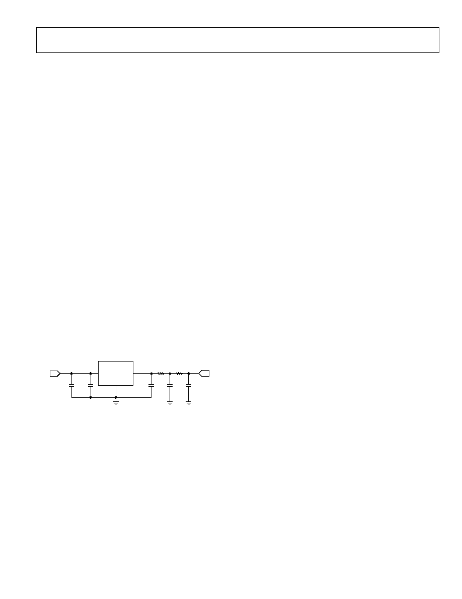
CLOCKING THE AD7763
The AD7763 requires an external, low jitter clock source. This
signal is applied to the MCLK pin, and the MCLKGND pin is
used to sense the ground from the clock source. An internal
clock signal (ICLK) is derived from the MCLK input signal.
The ICLK controls the internal operations of the AD7763. The
maximum ICLK frequency is 20 MHz, but due to an internal
clock divider, a range of MCLK frequencies can be used. There
are two ways to generate the ICLK:
ICLK = MCLK
(CDIV = 1)
ICLK = MCLK
/2 (CDIV = 0)
This option is pin selectable (Pin 58). On power-up, the default
is ICLK = MCLK/2 to ensure that the part can handle the maxi-
mum MCLK frequency of 40 MHz. For output data rates equal to
those used in audio systems, a 12.288 MHz ICLK frequency can
be used. As shown in Table 6, output data rates of 192 kHz, 96 kHz,
and 48 kHz are achievable with this ICLK frequency. As mentioned
previously, this ICLK frequency can be derived from different
MCLK frequencies.
The MCLK jitter requirements depend on a number of factors
and are determined by
20
)
dB
(
)
(
10
2
SNR
IN
rms
j
f
OSR
t
×
×
×
=
Where:
OSR
= oversampling ratio =
ODR
f
ICLK
.
f
IN
= maximum input frequency.
SNR
(dB) = target SNR.
EXAMPLE 1
This example is taken from Table 6, where:
ODR
= 625 kHz.
f
ICLK
= 20 MHz.
f
IN
(maximum) = 250 kHz.
SNR
= 108 dB.
ps
6
.
3
10
10
250
2
32
6
3
)
(
=
×
×
×
×
=
rms
j
t
This is the maximum allowable clock jitter for a full-scale,
250 kHz input tone with the given ICLK and output data rate.
EXAMPLE 2
Following is a second example from Table 6, where:
ODR
= 48 kHz.
f
ICLK
= 12.288 MHz.
f
IN
(maximum) = 19.2 kHz.
SNR
= 120 dB.
ps
133
10
10
2
.
19
2
256
6
3
)
(
=
×
×
×
×
=
rms
j
t
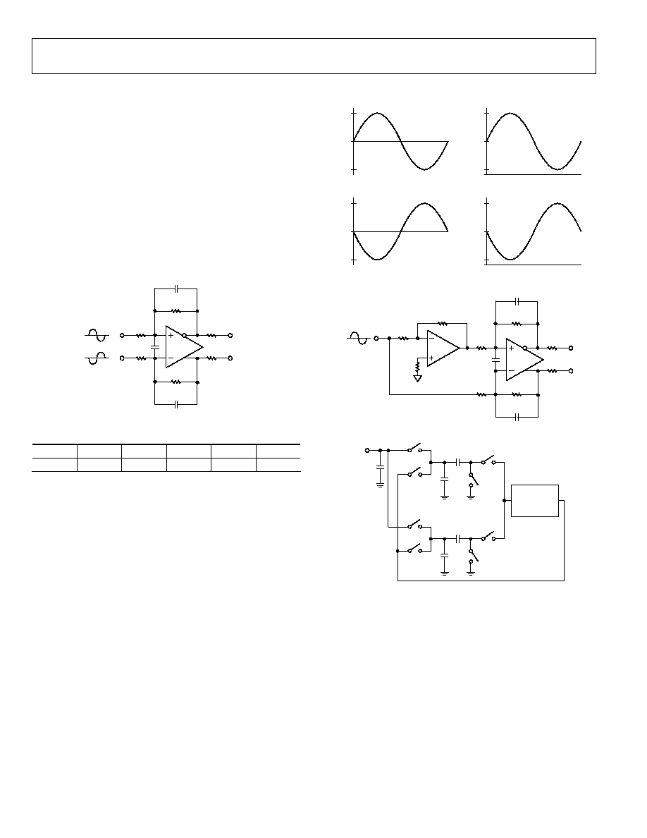
The input amplitude also has an effect on these jitter figures.
If, for example, the input level is 3 dB below full scale, the allowable
jitter is increased by a factor of 2, increasing the first example
to 2.53 ps rms. This happens when the maximum slew rate is
decreased by a reduction in amplitude. Figure 29 and Figure 30
illustrate this point, showing the maximum slew rate of a sine
wave of the same frequency but with different amplitudes.
1.0
1.0
05
47
6-
01
4
0.5
0
0.5
Figure 29. Maximum Slew Rate of Sine Wave with Amplitude of 2 V p-p
1.0
1.0
05
47
6-
01
5
0.5
0
0.5
Figure 30. Maximum Slew Rate of Same Frequency Sine Wave
with Amplitude of 1 V p-p
AD7763
Rev. 0 | Page 20 of 32
DRIVING THE AD7763
The AD7763 has an on-chip differential amplifier that operates
with a supply voltage (AV
DD3
) from 3.15 V to 5.25 V. For a 4.096 V
reference, the supply voltage must be 5 V.
To achieve the specified performance in normal mode, the
differential amplifier should be configured as a first-order
antialias filter, as shown in Figure 31. Any additional filtering
should be carried out in previous stages using low noise, high
performance op amps, such as the
AD8021
.
Suitable component values for the first-order filter are shown in
Table 10. The values in Table 10 yield a 10 dB attenuation at the
first alias point of 19 MHz.
0
54
76
-
01
6
A1
R
IN
R
FB
C
FB
R
IN
R
M
R
M
C
S
R
FB
C
FB
V
IN
A
B
V
IN
+
Figure 31. Differential Amplifier Configuration
Table 10. Normal Mode Component Values
V
REF
R
IN
R
FB
R
M
C
S
C
FB
4.096 V
1 k
655
18
5.6 pF
33 pF
Figure 32 shows the signal conditioning that occurs using the
circuit in Figure 18 with a ±2.5 V input signal biased around
ground and having the component values and conditions in
Table 10.
The differential amplifier always biases the output signal to sit
on the optimum common mode of V
REF
/2, in this case, 2.048 V.
The signal is also scaled to give the maximum allowable voltage
swing with this reference value. This is calculated as 80% of
V
REF
; that is, 0.8 × 4.096 V 3.275 V p-p on each input.
To obtain maximum performance from the AD7763, it is
advisable to drive the ADC with differential signals. Figure 33
shows how a bipolar, single-ended signal biased around ground
can drive the AD7763 with the use of an external op amp, such as
the
AD8021
.
With a 4.096 V reference, a 5 V supply must be provided to the
reference buffer (AV
DD4
). With a 2.5 V reference, a 3.3 V supply
must be provided to AV
DD4
.
054
76-
017
+2.5V
0V
2.5V
+2.5V
0V
2.5V
+3.685V
+2.048V
+0.410V
+3.685V
+2.048V
+0.410V
A
V
IN
+
V
IN
B
Figure 32. Differential Amplifier Signal Conditioning
0
54
76
-
01
8
A1
R
IN
R
FB
C
FB
R
IN
R
M
R
M
C
S
R
FB
C
FB
V
IN
V
IN
V
IN
+
AD8021
2R
2R
R
Figure 33. Single-Ended-to-Differential Conversion
0
547
6-
0
19
CS2
CPB2
SS4
SH4
CPA
SS2
SH2
CS1
CPB1
SS3
SH3
SS1
SH1
ANALOG
MODULATOR
V
IN
+
Figure 34. Equivalent Input Circuit
The AD7763 employs a double sampling front end, as shown in
Figure 34. For simplicity, only the equivalent input circuit for
V
IN
+ is shown. The equivalent input circuitry for V
IN
- is the same.
AD7763
Rev. 0 | Page 21 of 32
Sampling Switch SS1 and Sampling Switch SS3 are driven by ICLK,
whereas Sampling Switch SS2 and Sampling Switch SS4 are driven
by ICLK. When ICLK is high, the analog input voltage is connected
to CS1. On the falling edge of ICLK, the SS1 and SS3 switches
open, and the analog input is sampled on CS1. Similarly, when
ICLK is low, the analog input voltage is connected to CS2. On
the rising edge of ICLK, the SS2 and SS4 switches open, and the
analog input is sampled on CS2.
Capacitor CPA, Capacitor CPB1, and Capacitor CPB2 represent
parasitic capacitances that include the junction capacitances
associated with the MOS switches.
Table 11. Equivalent Component Values
Mode
CS1 CS2 CPA CPB1/CPB2
Normal
51 pF
51 pF
12 pF
20 pF
Low Power
13 pF
13 pF
12 pF
5 pF
USING THE AD7763
Following is the recommended sequence for powering up and
using the AD7763.
1. Apply power.
2. Start clock oscillator, applying MCLK.
3. Take RESET low for a minimum of 1 MCLK cycle.
4. Wait a minimum of 2 MCLK cycles after RESET has been
released.
5. Write to Control Register 2 to power up the ADC and the
differential amplifier, as required.
6. Write to Control Register 1 to set up the output data rate.
7. In circumstances where multiple parts are being
synchronized, a SYNC pulse must be applied to the parts;
otherwise, no SYNC pulse is required.
The following are conditions for applying the SYNC pulse:
· The issuing of a SYNC pulse to the part must not coincide
with a write to the part.
· The SYNC pulse should be applied a minimum
of 2.5 ICLK cycles after the FSI signal for the previous write
to the part has returned to logic high.
· Ensure that the SYNC pulse is taken low for a minimum of
2.5 ICLK cycles.
Data can now be read from the part using the default filter,
offset, gain, and overrange threshold values. The conversion
data read is not valid, however, until the settling time of the
filter has passed. When this has occurred, the DVALID bit read
is set, indicating that the data is indeed valid.
The user can then download a user-defined filter, if required
(see Downloading a User-Defined Filter). Values for gain, offset,
and overrange threshold registers can also be written or read at
this stage.
BIAS RESISTOR SELECTION
The AD7763 requires a resistor to be connected between the
R
BIAS
pin and AGND. The value for this resistor is dependent on
the reference voltage being applied to the device. The resistor
value should be selected to give a current of 25 A through the
resistor to ground. For a 2.5 V reference voltage, the correct
resistor value is 100 k; for a 4.096 V reference voltage, the
correct resistor value is 160 k.
AD7763
Rev. 0 | Page 22 of 32
DECOUPLING AND LAYOUT RECOMMENDATIONS
Due to the high performance nature of the AD7763, correct decoupling and layout techniques are required to obtain the performance as
stated within this data sheet. Figure 35 shows a simplified connection diagram for the AD7763.
INA+
INA
OUTA
OUTA+
VIN+
VIN
VREF
PI
N
1
4
PI
N
1
5
PI
N
4
PI
N
1
2
PI
N
6
PI
N
3
3
PI
N
2
4
PI
N
2
7
PI
N
4
4
PI
N
6
3
PI
N
4
1
R19
160k
C64
33pF
C7
100nF
AV
DD3
PIN 24
(VDIF1)
C54
100nF
L6
DV
DD
PIN 41
(DVDD)
C58
100nF
L8
AV
DD2
PIN 4
(RHS)
C48
100nF
L1
PIN 15
(VBIAS)
C50
100nF
L3
PIN 14
(LHS)
PIN 27
C62
100nF
L2
L9
AV
DD4
PIN 12
(VBUF)
C59
10nF
L4
R38
10
AV
DD1
PIN 5
(VMOD1)
C52
100nF
L5
PIN 33
(VMOD2)
C53
100nF
L11
V
DRIVE
PIN 44
(VDRV1)
C56
100nF
L7
PIN 63
(VDRV2)
C57
100nF
L12
V
IN
A+
V
IN
A
V
OUT
A
V
OUT
A+
DECAPA
DECAPB
V
IN
+
V
IN
V
REF
+
REFGND
R
BIAS
DGND
DGND
DGND
DGND
DGND
DGND
DGND
19
20
21
22
8
30
25
26
10
9
17
1
35
42
43
57
59
62
I
2
S
SCR
SCO
SDO
SDI
SDL
SCP
SH1
SH2
RESET
SYNC
DRDY
MCLK
MCLKGND
AG
ND1
AG
ND1
AG
ND2
AG
ND2
AG
ND2
AG
ND2
AG
ND2
AG
ND3
AG
ND3
AG
ND3
AG
ND3
AG
ND4
7
34
5
13
16
18
28
23
29
31
32
11
AV
DD
2
AV
DD
2
AV
DD
2
AV
DD
4
AV
DD
1
AV
DD
1
AV
DD
3
AV
DD
2
V
DR
I
V
E
V
DR
I
V
E
DV
DD
14
15
4
12
6
33
24
27
44
63
41
AD7763BSV
DGND
53
61
60
58
55
54
50
49
46
45
40
37
36
38
3
2
56
52
51
48
47
39
U2
FSI
FSO
SH0
CDIV
64
DGND
ADR1
ADR2
ADR0
RESET
SYNC
DRDY
MCLK
I
2
S
SCR
SCO
SDO
SDI
SDL
SCP
SH1
SH2
FSI
FSO
CDIV
SH0
ADR1
ADR2
ADR0
0547
6-
02
8
Figure 35. Simplified Connection Diagram
AD7763
Rev. 0 | Page 23 of 32
SUPPLY DECOUPLING
Every supply pin must be connected to the appropriate supply
via a ferrite bead and decoupled to the correct ground pin with
a 100 nF, 0603 case size, X7R dielectric capacitor. There are two
exceptions
· Pin 12 (AV
DD4
) must have a 10 resistor inserted between
the pin and a 10 nF decoupling capacitor.
· Pin 27 (AV
DD2
) does not require a separate decoupling
capacitor or a direct connection to the supply; instead,
it is connected to Pin 14 via an 8.2 nH inductor.
The ferrite beads that are used to connect each supply pin to the
appropriate power supply should have a characteristic impedance
of 600 to 1 M at frequencies around 100 MHz, a dc impedance
of 1 or less, and a rated current of 200 mA.
ADDITIONAL DECOUPLING
There are two other decoupling pins on the AD7763: Pin 8
(DECAPA) and Pin 30 (DECAPB). Pin 8 should be decoupled
with a 100 nF capacitor, and Pin 30 requires a 33 pF capacitor.
REFERENCE VOLTAGE FILTERING
A low noise reference source, such as the ADR431 (2.5 V) or
ADR434 (4.096 V), is suitable for use with the AD7763. The
reference voltage supplied to the AD7763 should be decoupled
and filtered, as shown in Figure 36.
The recommended scheme for the reference voltage supply
is a 100 series resistor connected to a 100 F tantalum
capacitor, followed by a series resistor of 10 , and finally, a
10 nF decoupling capacitor very close to the V
REF
pin.
054
76-
021
12V
PIN 10
VOUT
2 +VIN
6
4
C15
10
F
C9
100nF
C10
100nF
R30
100
R17
10
+
C46
10nF
C11
100
F
+
ADR434
GND
U3
Figure 36. Reference Connection
DIFFERENTIAL AMPLIFIER COMPONENTS
The correct components for use around the on-chip differential
amplifier are shown in Table 10. Matching the components on
both sides of the differential amplifier is important to minimize
distortion of the signal applied to the amplifier. A tolerance of
0.1% or better is required for these components. Symmetrical
routing of the tracks on both sides of the differential amplifier
also assists in achieving stated performance.
EXPOSED PADDLE
The AD7763 64-lead TQFP_EP employs a 6 mm × 6 mm exposed
paddle (see Figure 39). The paddle reduces the thermal
resistance of the package by providing a path of low thermal
resistance to the PCB and, in turn, increases the heat transfer
efficiency from the AD7763 package. Soldering the exposed
paddle to the AGND plane of the PCB is fundamental in
creating the conditions that allow the AD7763 package to
perform to the highest specifications possible.
LAYOUT CONSIDERATIONS
While using the correct components is essential to achieve
optimum performance, the correct layout is just as important.
The Design Tools section of the AD7763 product page on
the Analog Devices website contains the Gerber files for the
AD7763 evaluation board. These files should be used as a
reference when designing any system using the AD7763.
The location and orientation of some of the components
mentioned in previous sections are critical, and particular
attention must be paid to the components that are located close
to the AD7763. Locating these components farther away from
the devices can have a direct impact on the maximum
performance achievable.
The use of ground planes should also be carefully considered.
To ensure that the return currents through the decoupling
capacitors are flowing to the correct ground pin, the ground
side of the capacitors should be as close as possible to the ground
pin associated with that supply. A ground plane should not be
relied upon as the sole return path for decoupling capacitors,
because the return current path using ground planes is not
easily predicted.
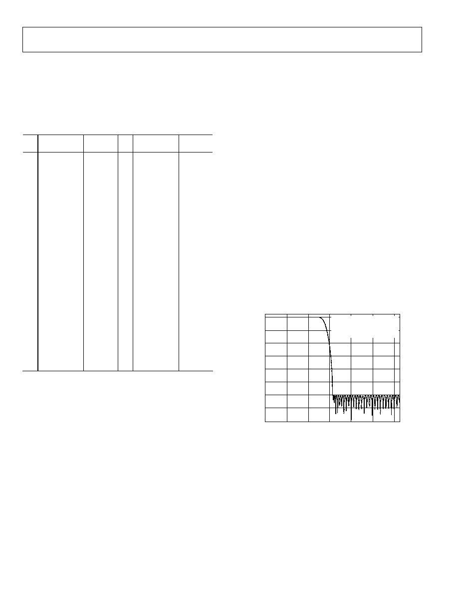
AD7763
Rev. 0 | Page 24 of 32
PROGRAMMABLE FIR FILTER
As discussed in the Theory of Operation section, the third FIR
filter on the AD7763 can be programmed by the user. The default
coefficients that are loaded on reset are shown in Table 12. This
gives the frequency response shown in Figure 37. The frequencies
shown in Figure 37 scale directly with the output data rate.
Table 12. Default Filter Coefficients
#
Decimal
Value
Hex
Value #
Decimal
Value
Hex
Value
0 +53656736 332BCA0 24
+700847
AB1AF
1 +25142688 17FA5A0 25
-70922
401150A
2 -4497814 444A196 26
-583959
408E917
3 -11935847 4B62067 27
-175934
402AF3E
4 -1313841 4140C31 28
+388667
5EE3B
5 +6976334 6A734E 29
+294000
47C70
6 +3268059 31DDDB 30
-183250
402CBD2
7 -3794610 439E6B2 31
-302597
4049E05
8 -3747402 4392E4A 32
+16034
3EA2
9 +1509849 1709D9 33
+238315
3A2EB
10 +3428088
344EF8 34 +88266
158CA
11 +80255
1397F
35 -143205
4022F65
12 -2672124
428C5FC 36 -128919
401F797
13 -1056628
4101F74 37 +51794
CA52
14 +1741563
1A92FB 38 +121875
1DC13
15 +1502200
16EBF8 39 +16426
402A
16 -835960
40CC178 40 -90524
401619C
17 -1528400
4175250 41 -63899
400F99B
18 +93626
16DBA
42 +45234
B0B2
19 +1269502
135EFE 43 +114720
1C020
20 +411245
6466D
44 +102357
18FD5
21 -864038
40D2F26 45 +52669
CDBD
22 -664622
40A242E 46 +15559
3CC7
23 +434489
6A139
47 +1963
7AB
The default filter should be sufficient for most applications.
It is a standard brick wall filter with a symmetrical impulse
response. The default filter has a length of 96 taps and is
nonaliasing, with 120 dB of attenuation at Nyquist. This filter
not only performs signal antialiasing but also suppresses out-of-
band quantization noise produced by the analog-to-digital
conversion process. Any significant relaxation in the stop-band
attenuation or transition bandwidth relative to the default filter
can result in failure to meet the SNR specifications.
To create a user-defined filter, note the following:
· The filter must be even, symmetrical FIR.
· The coefficients are 27 bits in length. All coefficients are
in sign-and-magnitude format. The sign bit coded as
positive = 0 is followed by 26 magnitude bits.
· The filter length must be between 12 taps and 96 taps in
steps of 12.
· Because the filter is symmetrical, the number of coefficients
that must be downloaded is half the filter length. The default
filter coefficients are an example of this, with only 48
coefficients listed for a 96-tap filter.
· Coefficients are written from the center of impulse response
(adjacent to the point of symmetry) outward.
· The coefficients are scaled so that the in-band gain
of the filter is equal to 134217726, with the coefficients
rounded to the nearest integer. For a low-pass filter, this is the
equivalent of having the coefficients sum arithmetically
(including sign) to +67108863 (0x3FFFFFF) positive value
over the half-impulse-response coefficient set (maximum 48
coefficients). Any deviation from this results in the
introduction of a gain error.
20
40
60
80
100
120
140
160
0
100
400
500
300
200
600
FREQUENCY (kHz)
AM
P
L
I
T
UD
E
(
d
B)
0
05
47
6-
02
2
0.1dB FREQUENCY = 251kHz
PASS-BAND RIPPLE = 0.05dB
STOP BAND = 312.5kHz
3dB FREQUENCY = 256kHz
Figure 37. Default Filter Frequency Response (625 kHz ODR)
To download a user-defined filter, see the Downloading a User-
Defined Filter section.
AD7763
Rev. 0 | Page 25 of 32
DOWNLOADING A USER-DEFINED FILTER
As discussed in the Programmable FIR Filter section, each of
the filter coefficients is 27 bits in length: one sign bit and 26 magni-
tude bits. To download coefficients for a user-specific FIR filter, a
32-bit word is written to the AD7763 for each coefficient.
D31 D30 D29 D28 D27 D26 D[25:0]
ALL ADR2 ADR1 ADR0 0
Sign Magnitude
When a user writes coefficients to one device, the address of that
particular device (as assigned by the ADR[2:0] pins) must be
specified in the bits labeled ADR[2:0].
In a configuration where more than one device shares the same SDI
line, setting the ALL bit to logic high and leaving Address Bits
ADR[2:0] logic low enables the user to write each coefficient to all
devices simultaneously.
To ensure that a filter is downloaded correctly, a checksum must
be generated and downloaded following the download of the final
coefficient. The checksum is a 16-bit word generated by splitting
each 32-bit word into 4 bytes and summing all bytes from all
coefficients up to a maximum of 192 bytes (maximum number
of coefficients = 48 bytes × 4 bytes written for each coefficient).
The checksum is written to the device in the form of a 32-bit word
in the following format:
D31
D30 D29 D28 D[27:16] D[15:0]
ALL ADR2 ADR1 ADR0 0
Checksum
Note that when writing the checksum, the addressing requirements
are as before, and Bit 27 to Bit 16 are all set to 0.
The same checksum is generated internally in the AD7763 and
compared with the checksum downloaded. The DL_OK bit in
the status register is set if these two checksums agree.
To download a user-defined filter:
1. Write to Control Register 1, setting the DL Filt bit. The
correct Filter Length Bits FLEN[3:0] correspond
to the length of the filter about to be downloaded
(see Table 13) and the correct decimation rate.
2. Write the 32-bit word (as per format specified). The
first coefficient to be written must be the one adjacent
to the point of filter symmetry.
3. Repeat Step 2 for each coefficient.
4. Implement the checksum write as per the specified
format.
5. Use the following methods to verify that the filter
coefficients have been downloaded correctly:
· Read the status register, checking the DL_OK bit.
· Start reading data and observe the status of the
DL_OK bit.
Note that because the user coefficients are stored in RAM, they
are cleared after a RESET operation or a loss of power.
Table 13. Filter Length Values
FLEN[3:0]
Number of Coefficients
Filter Length
0000 Default
Default
0001 6
12
0011 12
24
0101 18
36
0111 24
48
1001 30
60
1011 36
72
1101 42
84
1111 48
96
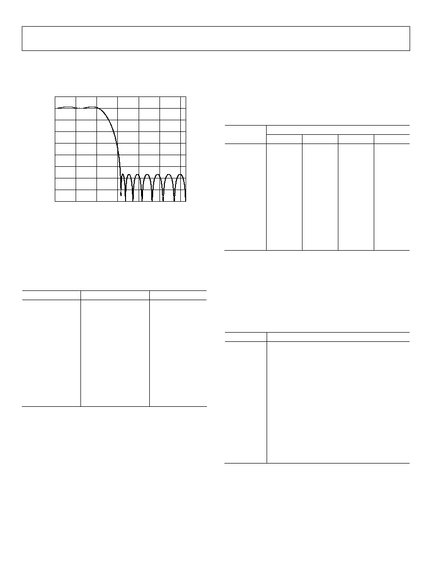
AD7763
Rev. 0 | Page 26 of 32
EXAMPLE FILTER DOWNLOAD
The following is an example of downloading a short, user-defined
filter with 24 taps. The frequency response is shown in Figure 38.
10
80
0
600
FREQUENCY (kHz)
AM
P
L
I
T
U
D
E
(
d
B)
0
10
20
30
40
50
60
70
100
200
300
400
500
05
47
6-
0
23
Figure 38. 24-Tap FIR Frequency Response
The coefficients for the filter in Table 14 are shown from the center
of symmetry outward; that is, Coefficient 1 is the coefficient at the
center of symmetry. The raw coefficients were generated using a
commercial filter design tool and scaled appropriately so their
sum equals 67108863 (0x3FF FFFF).
Table 14. 24-Tap FIR Coefficients
Coefficient Raw
Scaled
1 +0.365481974
+53188232
2 +0.201339905
+29300796
3 +0.009636604
+1402406
4 -0.075708848
-11017834
5 -0.042856209
-6236822
6 +0.019944246
+2902466
7 +0.036437914
+5302774
8 +0.007592007
+1104856
9 -0.021556583
-3137108
10 -0.024888355
-3621978
11 -0.012379538
-1801582
12 -0.001905756
-277343
Table 15 shows the 32-bit word (as per the format shown in the
Downloading a User-Defined Filter section) in hexadecimal for
each of the coefficients that must be written to the AD7763 to
realize this filter. The table is also split into the bytes that are all
summed to produce the checksum. The checksum generated
from these coefficients is 0x0E6B.
Table 15. Filter Hex Values
1
32-Bit Word Written to Download Coefficient
Coefficient
Byte 1
Byte 2
Byte 3
Byte 4
1
03 2B 96 88
2
01 BF 18 3C
3
00 15 66 26
4 04
A8
1E
6A
5 04
5F
2A
96
6
00 2C 49 C2
7
00 50 E9 F6
8
00 10 DB D8
9 04
2F
DE
54
10 04 37 44 5A
11 04
1B
7D
6E
12 04 04 3B 5F
1
All values of words listed are with reference to writing to one device only
(ALL = 0) with Address 000 (as assigned to the device using the ADR[2:0]
pins).
Table 16 lists in hexadecimal format the sequence of 32-bit
words the user writes to the AD7763 to set up the ADC and
download this filter, assuming selection of an output data rate
of 625 kHz.
Table 16.
Word
1
Description
0x0001807A
Address of Control Register 1. Control register
data. DL filter, set filter length = 24, set output
data rate = 625 kHz.
0x032B9688 First
coefficient.
0x01BF183C Second
coefficient.
...
Other coefficients.
0x04043B5F
Twelfth (final) coefficient.
0x00000E6B
Checksum. Wait (0.5 × t
ICLK
× number of unused
coefficients) for AD7763 to fill remaining unused
coefficients with 0s.
0x0001087A
Address of Control Register. Control register data.
Set read status and maintain filter length and
decimation settings. Read contents of status
register. Check Bit 7 (DL_OK) to determine that
the filter downloaded correctly.
1
All values of words listed are with reference to writing to one device only
(ALL = 0) with Address 000 (as assigned to the device using the ADR[2:0]
pins).
AD7763
Rev. 0 | Page 27 of 32
REGISTERS
The AD7763 has a number of user-programmable registers. The control registers are used to set the decimation rate, the filter configuration,
the low power option, and the control of the differential amplifier. There are also digital gain, offset, and overrange threshold registers.
Writing to these registers involves writing the register address first, followed by a 16-bit data-word. Register addresses, details of individual bits,
and default values are shown here.
CONTROL REGISTER 1--ADDRESS 0X001
Default Value 0x001A
MSB
LSB
DL Filt
RD Ovr
RD Gain
RD Off
RD Stat
0
SYNC
FLEN3
FLEN2
FLEN1
FLEN0
BYP F3
1 DEC2 DEC1 DEC0
Table 17.
Bit Mnemonic
Comment
15 DL
Filt
1
Download Filter. Before downloading a user-defined filter, this bit must be set. The filter length bits must also
be set at this time. The write operations that follow are interpreted as the user coefficients for the FIR filter until
all the coefficients and the checksum have been written.
14 RD
Ovr
1, 2
Read Overrange. If this bit is set, the next read operation outputs the contents of the overrange threshold register
instead of a conversion result.
13 RD
Gain
1, 2
Read Gain. If this bit is set, the next read operation outputs the contents of the digital gain register.
12 RD
Off
,
1
2
Read Offset. If this bit is set, the next read operation outputs the contents of the digital offset register.
11 RD
Stat
1,
2
Read Status. If this bit is set, the next read operation outputs the contents of the status register.
10
0
0 must be written to this bit.
9 SYNC
1
Synchronize. Setting this bit initiates an internal synchronization routine. Setting this bit simultaneously
on multiple devices synchronizes all filters.
8 to 5
FLEN[3:0]
Filter Length Bits. These bits must be set when the DL Filt bit is set and before a user-defined filter is downloaded.
4
BYP F3
Bypass Filter 3. If this bit is a 0, Filter 3 (programmable FIR) is bypassed.
3
1
1 must be written to this bit.
2 to 0
DEC[2:0]
Decimation Rate. These bits set the decimation rate of Filter 2. Writing a value of 0, 1, or 2 corresponds to
4× decimation. A value of 3 corresponds to 8× decimation; a value of 4 corresponds to 16×; and the
maximum value of 5 corresponds to 32× decimation.
1
Bit 15 to Bit 9 are all self-clearing bits.
2
Only one of these bits can be set in any write operation, because they all determine the contents of the next operation.
CONTROL REGISTER 2--ADDRESS 0X002
Default Value 0x009B
MSB
LSB
0
0 0 0 0 0 0 0 0 0 0 0 PD
LPWR
1 D1PD
Table 18.
Bit Mnemonic Comment
3
PD
Power Down. Setting this bit powers down the AD7763, reducing the power consumption to 6.35 mW.
2 LPWR
Low Power. If this bit is set, the AD7763 operates in a low power mode. The power consumption is reduced for a 3 dB
reduction in noise performance.
1
1
1 must be written to this bit.
0
D1PD
Differential Amplifier Power Down. Setting this bit powers down the on-chip differential amplifier.
AD7763
Rev. 0 | Page 28 of 32
STATUS REGISTER (READ ONLY)
MSB
LSB
PART 1
PART 0
DIE 2
DIE 1
DIE 0
0
LPWR
OVR
DL_OK
FILTER_OK
UFILTER
BYP F3
1 DEC2 DEC1 DEC0
Table 19.
Bit Mnemonic
Comment
15,14
PART[1:0]
Part Number. These bits are constant for the AD7763.
13 to 11
DIE[2:0]
Die Number. These bits reflect the current AD7763 die number for identification purposes within a system.
10
0
0 must be written to this bit.
9
LPWR
Low Power. If the AD7763 is operating in low power mode, this bit is set to 1.
8
OVR
If the current analog input exceeds the current overrange threshold, this bit is set.
7 DL_OK
When downloading a user filter to the AD7763, a checksum is generated. This checksum is compared to
the one downloaded following the coefficients. If these checksums agree, this bit is set.
6 FILTER_OK
When a user-defined filter is in use, a checksum is generated when the filter coefficients pass through
the filter. This generated checksum is compared to the one downloaded. If they match, this bit is set.
5
UFILTER
If a user-defined filter is in use, this bit is set.
4
BYP F3
Bypass Filter 3. If Filter 3 is bypassed by setting the relevant bit in Control Register 1, this bit is also set.
3
1
1 must be written to this bit.
2 to 0
DEC[2:0]
Decimation Rate. These bits correspond to the bits set in Control Register 1.
OFFSET REGISTER--ADDRESS 0X003
Non Bit-Mapped, Default Value 0x0000
The offset register uses twos complement notation and is scaled so
that 0x7FFF (maximum positive value) and 0x8000 (maximum
negative value) correspond to an offset of +0.390625% and
-0.390625%, respectively. Offset correction is applied after any gain
correction. Using the default gain value of 1.25 and assuming a
reference voltage of 4.096 V, the offset correction range is
approximately ±25 mV.
GAIN REGISTER--ADDRESS 0X004
Non Bit-Mapped, Default Value 0xA000
The gain register is scaled so that 0x8000 corresponds to a gain
of 1.0. The default value of this register is 1.25 (0xA000). This
gives a full-scale digital output when the input is at 80% of V
REF
.
This ties in with the maximum analog input range of ±80% of
V
REF
p-p.
OVERRANGE REGISTER--ADDRESS 0X005
Non Bit-Mapped, Default Value 0xCCCC
The overrange register value is compared with the output of the
first decimation filter to obtain an overload indication with
minimum propagation delay. This is prior to any gain scaling or
offset adjustment. The default value is 0xCCCC, which
corresponds to 80% of V
REF
(the maximum permitted analog
input voltage). Assuming V
REF
= 4.096 V, the bit is then set when
the input voltage exceeds approximately 6.55 V p-p differential.
Note that the overrange bit is also set immediately if the analog
input voltage exceeds 100% of V
REF
for more than 4 consecutive
samples at the modulator rate.
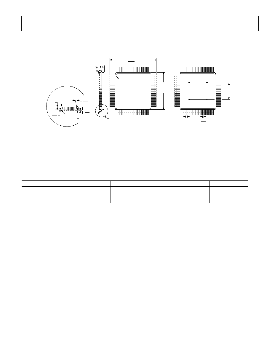
AD7763
Rev. 0 | Page 29 of 32
OUTLINE DIMENSIONS
COMPLIANT TO JEDEC STANDARDS MS-026-ACD-HD
1.05
1.00
0.95
0.20
0.09
0.08 MAX
COPLANARITY
VIEW A
ROTATED 90
°
CCW
SEATING
PLANE
0° MIN
7°
3.5°
0°
0.15
0.05
49
64
1
17
16
32
33
48
1.20
MAX
0.75
0.60
0.45
VIEW A
TOP VIEW
(PINS DOWN)
PIN 1
49
64
17
1
16
32
33
48
0.50
BSC
LEAD PITCH
0.38
0.32
0.22
BOTTOM VIEW
(PINS UP)
6.00
BSC SQ
EXPOSED
PAD
12.20
12.00 SQ
11.80
10.20
10.00 SQ
9.80
Figure 39. 64-Lead Thin Quad Flat Package, Exposed Pad [TQFP_EP]
(SV-64-2)
Dimensions shown in millimeters
ORDERING GUIDE
Model
Temperature Range
Package Description
Package Option
AD7763BSVZ
1
-40°C to +85°C
64-Lead Thin Quad Flat Package, Exposed Pad (TQFP_EP)
SV-64-2
AD7763BSVZ-REEL
1
-40°C to +85°C
64-Lead Thin Quad Flat Package, Exposed Pad (TQFP_EP)
SV-64-2
EVAL-AD7763EB
Evaluation
Board
1
Z = Pb-free part.

AD7763
Rev. 0 | Page 30 of 32
NOTES

AD7763
Rev. 0 | Page 31 of 32
NOTES

AD7763
Rev. 0 | Page 32 of 32
NOTES
© 2005 Analog Devices, Inc. All rights reserved. Trademarks and
registered trademarks are the property of their respective owners.
D05476-0-10/05(0)
Document Outline
- þÿ
- þÿ
- þÿ
- þÿ
- þÿ
- REVISION HISTORY
- þÿ
- þÿ
- þÿ
- þÿ
- þÿ
- þÿ
- þÿ
- þÿ
- þÿ
- þÿ
- þÿ
- þÿ
- þÿ
- þÿ
- þÿ