Document Outline
- Specifications
- Pinout
- OUTLINE DIMENSIONS
- Ordering Guide
- Features
- Applications
- Absolute Maximum Ratings
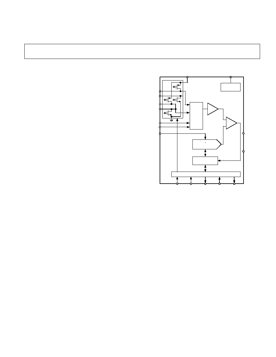
- Functional Block Diagram
- Pin Function Description
- Typical Characteristics
- PRODUCT DESCRIPTION
- PRODUCT HIGHLIGHTS
- CAUTION
- ADC TRANSFER FUNCTION
- CIRCUIT INFORMATION TYPICAL CONNECTION DIAGRAM
- MODE
- CONTROL REGISTER
- POWER VS. THROUGHPUT RATE
- PEN INTERRUPT REQUEST
- GROUNDING AND LAYOUT
- DIAGRAMS
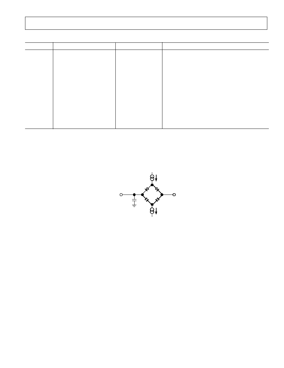
- Load Circuit for Digital Output Timing Specifications
- Typical Application Circuit
- Equivalent Analog Input Circuit
- Single-Ended Reference Mode (SER/DFR = 1)
- Reference Input Circuitry
- Differential Reference Mode (SER/DFR = 0)
- Conversion Timing, 24 DCLKS per Conversion Cycle, 8-Bit Bus Interface. No DCLK delay required with dedicated serial port
- Detailed Timing Diagram
- Conversion Timing, 16 DCLKS per Cycle, 8-Bit Bus Interface. No DCLK Delay Required with Dedicated Serial Port
- Conversion Timing, 15 DCLKS per Cycle, Maximum Throughput Rate
- PENIRQ Functional Block Diagram
- PENIRQ Timing Diagram
REV. 0
Information furnished by Analog Devices is believed to be accurate and
reliable. However, no responsibility is assumed by Analog Devices for its
use, nor for any infringements of patents or other rights of third parties
which may result from its use. No license is granted by implication or
otherwise under any patent or patent rights of Analog Devices.
a
AD7843
One Technology Way, P.O. Box 9106, Norwood, MA 02062-9106, U.S.A.
Tel: 781/329-4700
World Wide Web Site: http://www.analog.com
Fax: 781/326-8703
© Analog Devices, Inc., 2000
Touch Screen Digitizer
FUNCTIONAL BLOCK DIAGRAM
PEN
INTERRUPT
DCLK
GND
+V
CC
BUSY
PENIRQ
SAR + ADC
CONTROL LOGIC
SPORT
CS
DOUT
DIN
4-TO-1
I/P
MUX
AD7843
+V
CC
IN3
V
REF
IN4
Y≠
Y+
X≠
X+
T/H
CHARGE
REDISTRIBUTION
DAC
COMP
GENERAL DESCRIPTION
The AD7843 is a 12-bit successive-approximation ADC with a
synchronous serial interface and low on resistance switches for
driving touch screens. The part operates from a single 2.2 V to
5.25 V power supply and features throughput rates greater than
125 kSPS.
The external reference applied to the AD7843 can be varied
from 1 V to +V
CC
, while the analog input range is from 0 V to
V
REF
. The device includes a shutdown mode that reduces the
current consumption to less than 1
µA.
The AD7843 features on-board switches. This coupled with low
power and high-speed operation make this device ideal for
battery-powered systems such as personal digital assistants with
resistive touch screens and other portable equipment. The part
is available in a 16-lead 0.15" Quarter Size Outline (QSOP) pack-
age and a 16-lead Thin Shrink Small Outline (TSSOP) package.
FEATURES
4-Wire Touch Screen Interface
Specified Throughput Rate of 125 kSPS
Low Power Consumption:
1.37 mW Max at 125 kSPS with V
CC
= 3.6 V
Single Supply, V
CC
of 2.2 V to 5.25 V
Ratiometric Conversion
High-Speed Serial Interface
Programmable 8- or 12-Bit Resolution
Two Auxiliary Analog Inputs
Shutdown Mode: 1 A max
16-Lead QSOP and TSSOP Packages
APPLICATIONS
Personal Digital Assistants
Smart Hand-Held Devices
Touch Screen Monitors
Point-of-Sales Terminals
Pagers
PRODUCT HIGHLIGHTS
1. Ratiometric conversion mode available eliminating errors
due to on-board switch resistances.
2. Maximum current consumption of 380
µA while operating at
125 kSPS.
3. Power-down options available.
4. Analog input range from 0 V to V
REF
.
5. Versatile serial I/O port.
REV. 0
≠2≠
AD7843≠SPECIFICATIONS
(V
CC
= 2.7 V to 3.6 V, V
REF
= 2.5 V, f
SCLK
= 2 MHz unless otherwise noted; T
A
=
≠40 C to +85 C, unless otherwise noted.)
Parameter
AD7843A
1
Unit
Test Conditions/Comments
DC ACCURACY
Resolution
12
Bits
No Missing Codes
11
Bits min
Integral Nonlinearity
2
±2
LSB max
Offset Error
2
±6
LSB max
V
CC
= 2.7 V
Offset Error Match
3
1
LSB max
0.1
LSB typ
Gain Error
2
±4
LSB max
Gain Error Match
3
1
LSB max
0.1
LSB typ
Power Supply Rejection
70
dB typ
SWITCH DRIVERS
On-Resistance
2
Y+, X+
5
typ
Y≠, X≠
6
typ
ANALOG INPUT
Input Voltage Ranges
0 to V
REF
Volts
DC Leakage Current
±0.1
µA typ
Input Capacitance
37
pF typ
REFERENCE INPUT
V
REF
Input Voltage Range
1.0/+V
CC
V min/max
DC Leakage Current
±1
µA max
V
REF
Input Impedance
5
G
typ
CS = GND or +V
CC
V
REF
Input Current
3
20
µA max
8
µA typ
1
µA typ
f
SAMPLE
= 12.5 kHz
1
µA max
CS = +V
CC
; 0.001
µA typ
LOGIC INPUTS
Input High Voltage, V
INH
2.4
V min
Input Low Voltage, V
INL
0.4
V max
Input Current, I
IN
±1
µA max
Typically 10 nA, V
IN
= 0 V or +V
CC
Input Capacitance, C
IN
4
10
pF max
LOGIC OUTPUTS
Output High Voltage, V
OH
V
CC
≠ 0.2
V min
I
SOURCE
= 250
µA; V
CC
= 2.2 V to 5.25 V
Output Low Voltage, V
OL
0.4
V max
I
SINK
= 250
µA
PENIRQ Output Low Voltage, V
OL
0.4
V max
I
SINK
= 250
µA; 100 k Pull-Up
Floating-State Leakage Current
±10
µA max
Floating-State Output Capacitance
4
10
pF max
Output Coding
Straight (Natural) Binary
CONVERSION RATE
Conversion Time
12
DCLK Cycles max
Track/Hold Acquisition Time
3
DCLK Cycles min
Throughput Rate
125
kSPS max
POWER REQUIREMENTS
V
CC
(Specified Performance)
2.7/3.6
V min/max
Functional from 2.2 V to 5.25 V
I
CC
5
Digital I/Ps = 0 V or V
CC
Normal Mode (f
SAMPLE
= 125 kSPS)
380
µA max
V
CC
= 3.6 V, 240
µA typ
Normal Mode (f
SAMPLE
= 12.5 kSPS)
170
µA typ
V
CC
= 2.7 V, f
DCLK
= 2 00 kHz
Normal Mode (Static)
150
µA typ
V
CC
= 3.6 V
Shutdown Mode (Static)
1
µA max
Power Dissipation
5
Normal Mode (f
SAMPLE
= 125 kSPS)
1.368
mW max
V
CC
= 3.6 V
Shutdown
3.6
µW max
V
CC
= 3.6 V
NOTES
1
Temperature range as follows: A Version: ≠40
∞C to +85∞C.
2
See Terminology.
3
Guaranteed by design.
4
Sample tested @ 25
∞C to ensure compliance.
5
See Power vs. Throughput Rate section.
Specifications subject to change without notice.
REV. 0
AD7843
≠3≠
Parameter
Limit at T
MIN
, T
MAX
Unit
Description
f
DCLK
2
10
kHz min
2
MHz max
t
ACQ
1.5
µs min
Acquisition Time
t
1
10
ns min
CS Falling Edge to First DCLK Rising Edge
t
2
60
ns max
CS Falling Edge to BUSY Three-State Disabled
t
3
3
60
ns max
CS Falling Edge to DOUT Three-State Disabled
t
4
200
ns min
DCLK High Pulsewidth
t
5
200
ns min
DCLK Low Pulsewidth
t
6
60
ns max
DCLK Falling Edge to BUSY Rising Edge
t
7
10
ns min
Data Setup Time Prior to DCLK Rising Edge
t
8
10
ns min
Data Valid to DCLK Hold Time
t
9
3
200
ns max
Data Access Time after DCLK Falling Edge
t
10
0
ns min
CS Rising Edge to DCLK Ignored
t
11
200
ns max
CS Rising Edge to BUSY High Impedance
t
12
4
200
ns max
CS Rising Edge to DOUT High Impedance
NOTES
1
Sample tested at 25
∞C to ensure compliance. All input signals are specified with tr = tf = 5 ns (10% to 90% of V
CC
) and timed from a voltage level of 1.6 V.
2
Mark/Space ratio for the SCLK input is 40/60 to 60/40.
3
Measured with the load circuit of Figure 1 and defined as the time required for the output to cross 0.4 V or 2.0 V.
4
t
12
is derived from the measured time taken by the data outputs to change 0.5 V when loaded with the circuit of Figure 1. The measured number is then extrapolated
back to remove the effects of charging or discharging the 50 pF capacitor. This means that the time, t
12
, quoted in the timing characteristics is the true bus relinquish
time of the part and is independent of the bus loading.
Specifications subject to change without notice.
TIMING SPECIFICATIONS
1
(T
A
= T
MIN
to T
MAX
, unless otherwise noted; V
CC
= 2.7 V to 3.6 V, V
REF
= 2.5 V)
TO
OUTPUT
PIN
C
L
50pF
1.6V
I
OL
200 A
I
OH
200 A
Figure 1. Load Circuit for Digital Output Timing Specifications
REV. 0
AD7843
≠4≠
CAUTION
ESD (electrostatic discharge) sensitive device. Electrostatic charges as high as 4000 V readily
accumulate on the human body and test equipment and can discharge without detection. Although
the AD7843 features proprietary ESD protection circuitry, permanent damage may occur on
devices subjected to high-energy electrostatic discharges. Therefore, proper ESD precautions are
recommended to avoid performance degradation or loss of functionality.
WARNING!
ESD SENSITIVE DEVICE
ABSOLUTE MAXIMUM RATINGS
1
(T
A
= 25
∞C unless otherwise noted)
+V
CC
to GND . . . . . . . . . . . . . . . . . . . . . . . . . ≠0.3 V to +7 V
Analog Input Voltage to GND . . . . . . . ≠0.3 V to V
CC
+ 0.3 V
Digital Input Voltage to GND . . . . . . . ≠0.3 V to V
CC
+ 0.3 V
Digital Output Voltage to GND . . . . . ≠0.3 V to V
CC
+ 0.3 V
V
REF
to GND . . . . . . . . . . . . . . . . . . . . ≠0.3 V to V
CC
+ 0.3 V
Input Current to Any Pin Except Supplies
2
. . . . . . .
±10 mA
Operating Temperature Range
Commercial . . . . . . . . . . . . . . . . . . . . . . . . ≠40
∞C to +85∞C
Storage Temperature Range . . . . . . . . . . . ≠65
∞C to +150∞C
Junction Temperature . . . . . . . . . . . . . . . . . . . . . . . . . . 150
∞C
QSOP, TSSOP Package, Power Dissipation . . . . . . . 450 mW
JA
Thermal Impedance . . . . . . . . . . . 149.97
∞C/W (QSOP)
. . . . . . . . . . . . . . . . . . . . . . . . . . . . . . . 150.4
∞C/W (TSSOP)
JC
Thermal Impedance . . . . . . . . . . . . . 38.8
∞C/W (QSOP)
. . . . . . . . . . . . . . . . . . . . . . . . . . . . . . . . 27.6
∞C/W (TSSOP)
Lead Temperature, Soldering
Vapor Phase (60 secs) . . . . . . . . . . . . . . . . . . . . . . . 215
∞C
Infrared (15 secs) . . . . . . . . . . . . . . . . . . . . . . . . . . 220
∞C
NOTES
1
Stresses above those listed under Absolute Maximum Rating may cause permanent
damage to the device. This is a stress rating only; functional operation of the device
at these or any other conditions above those listed in the operational sections of this
specification is not implied. Exposure to absolute maximum rating conditions for
extended periods may affect device reliability.
2
Transient currents of up to 100 mA will not cause SCR latch-up.
ORDERING GUIDE
Temperature
Linearity
Package
Package
Branding
Model
Range
Error (LSB)
1
Option
Description
Information
AD7843ARQ
≠40
∞C to +85∞C
±2
RQ-16
2
QSOP
AD7843ARQ
AD7843ARQ-REEL
≠40
∞C to +85∞C
±2
RQ-16
2
QSOP
AD7843ARQ
AD7843ARQ-REEL7
≠40
∞C to +85∞C
±2
RQ-16
2
QSOP
AD7843ARQ
AD7843ARU
≠40
∞C to +85∞C
±2
RU-16
TSSOP
AD7843ARU
AD7843ARU-REEL
≠40
∞C to +85∞C
±2
RU-16
TSSOP
AD7843ARU
AD7843ARU-REEL7
≠40
∞C to +85∞C
±2
RU-16
TSSOP
AD7843ARU
EVAL-AD7843CB
3
Evaluation Board
EVAL-CONTROL BRD2
4
Controller Board
NOTES
1
Linearity error here refers to integral linearity error.
2
RQ = 0.15" Quarter Size Outline Package.
3
This can be used as a stand-alone evaluation board or in conjunction with the EVALUATION BOARD CONTROLLER for evaluation/demonstration purposes.
4
This EVALUATION BOARD CONTROLLER is a complete unit allowing a PC to control and communicate with all Analog Devices evaluation boards ending in the
CB designators.
PIN CONFIGURATION QSOP/TSSOP
TOP VIEW
(Not to Scale)
16
15
14
13
12
11
10
9
1
2
3
4
5
6
7
8
+V
CC
X+
Y+
X≠
Y≠
GND
IN3
IN4
DCLK
CS
DIN
BUSY
DOUT
PENIRQ
+V
CC
VREF
AD7843
REV. 0
AD7843
≠5≠
PIN FUNCTION DESCRIPTIONS
Pin
No.
Mnemonic
Function
1, 10
+V
CC
Power Supply Input. The +V
CC
range for the AD7843 is from 2.2 V to 5.25 V. Both +V
CC
pins should
be connected directly together.
2
X+
X+ Position Input. ADC Input Channel 1.
3
Y+
Y+ Position Input. ADC Input Channel 2.
4
X≠
X≠ Position Input.
5
Y≠
Y≠ Position Input.
6
GND
Analog Ground. Ground reference point for all circuitry on the AD7843. All analog input signals and
any external reference signal should be referred to this GND voltage.
7
IN3
Auxiliary Input 1. ADC Input Channel 3.
8
IN4
Auxiliary Input 2. ADC Input Channel 4.
9
V
REF
Reference Input for the AD7843. An external reference must be applied to this input. The voltage
range for the external reference is 1.0 V to +V
CC
. For specified performance it is 2.5 V.
11
PENIRQ
Pen Interrupt. CMOS Logic open drain output (requires 10 k
to 100 k pull-up resistor externally).
12
DOUT
Data Out. Logic Output. The conversion result from the AD7843 is provided on this output as a
serial data stream. The bits are clocked out on the falling edge of the DCLK input. This output is
high impedance when
CS is high.
13
BUSY
BUSY Output. Logic Output. This output is high impedance when
CS is high.
14
DIN
Data In. Logic Input. Data to be written to the AD7843's Control Register is provided on this input
and is clocked into the register on the rising edge of DCLK (see Control Register section).
15
CS
Chip Select Input. Active Low Logic Input. This input provides the dual function of initiating con-
versions on the AD7843 and also enables the serial input/output register.
16
DCLK
External Clock Input. Logic Input. DCLK provides the serial clock for accessing data from the part.
This clock input is also used as the clock source for the AD7843's conversion process.
TERMINOLOGY
Integral Nonlinearity
This is the maximum deviation from a straight line passing
through the endpoints of the ADC transfer function. The end-
points of the transfer function are zero scale, a point 1 LSB
below the first code transition, and full scale, a point 1 LSB
above the last code transition.
Differential Nonlinearity
This is the difference between the measured and the ideal 1 LSB
change between any two adjacent codes in the ADC.
Offset Error
This is the deviation of the first code transition (00 . . . 000) to
(00 . . . 001) from the ideal, i.e., AGND + 1 LSB.
Gain Error
This is the deviation of the last code transition (111 . . . 110) to
(111 . . . 111) from the ideal (i.e., V
REF
≠ 1 LSB) after the offset
error has been adjusted out.
Track/Hold Acquisition Time
The track/hold amplifier enters the acquisition phase on the fifth
falling edge of DCLK after the START bit has been detected.
Three DCLK cycles are allowed for the Track/Hold acquisition
time and the input signal will be fully acquired to the 12-bit
level within this time even with the maximum specified DCLK
frequency. See Analog Input section for more details.
On-Resistance
This is a measure of the ohmic resistance between the drain and
source of the switch drivers.