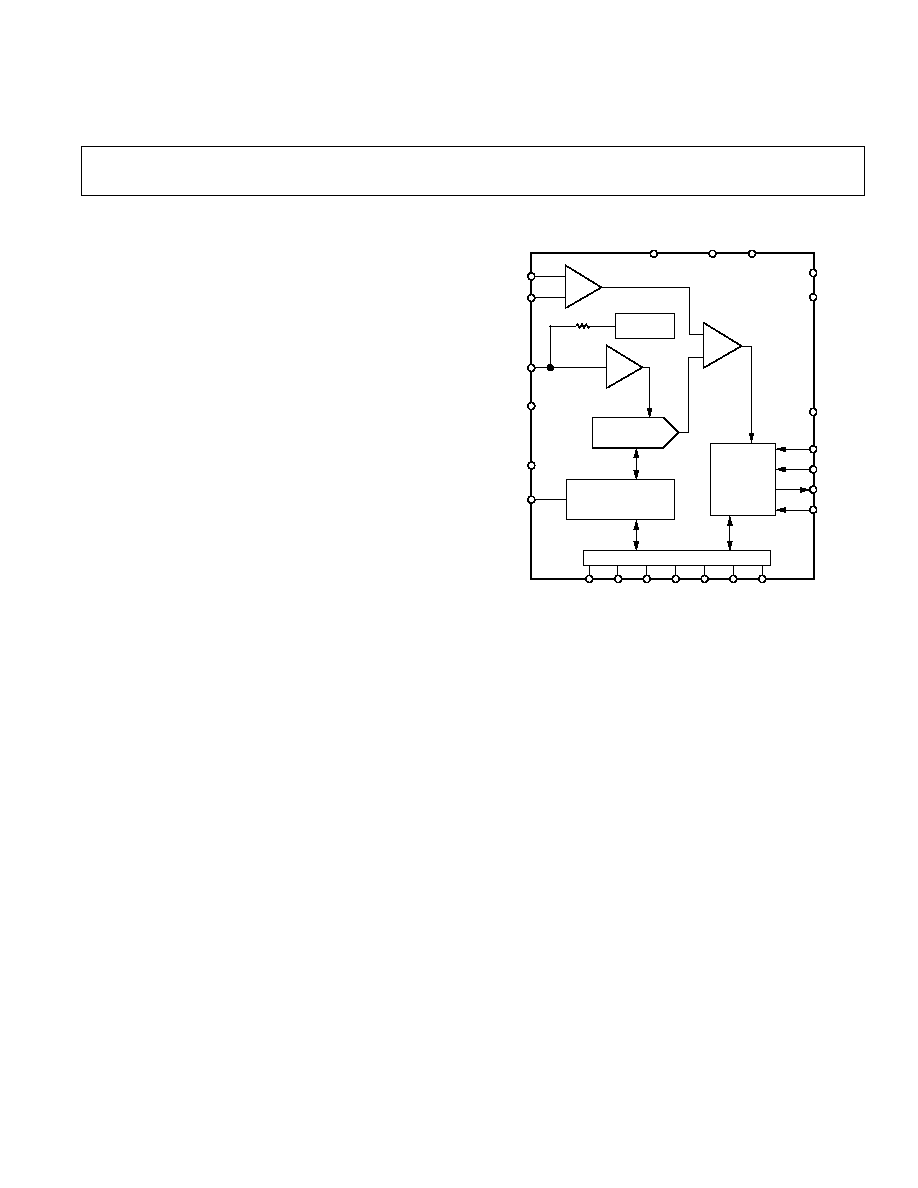
FUNCTIONAL BLOCK DIAGRAM
2.5V
REFERENCE
CALIBRATION
MEMORY
AND CONTROLLER
SAR + ADC
CONTROL
AV
DD
AGND
DV
DD
DGND
CLKIN
CONVST
BUSY
SLEEP
CAL
C
REF2
C
REF1
REF
IN
/
REF
OUT
AIN(≠)
AIN(+)
AMODE
SM1
SCLK
SYNC
POLARITY
DOUT
DIN
SM2
AGND
BUF
T/H
COMP
CHARGE
REDISTRIBUTION
DAC
SERIAL INTERFACE / CONTROL REGISTER
AD7853/AD7853L
REV. B
Information furnished by Analog Devices is believed to be accurate and
reliable. However, no responsibility is assumed by Analog Devices for its
use, nor for any infringements of patents or other rights of third parties
which may result from its use. No license is granted by implication or
otherwise under any patent or patent rights of Analog Devices.
a
3 V to 5 V Single Supply, 200 kSPS
12-Bit Sampling ADCs
AD7853/AD7853L*
FEATURES
Specified for V
DD
of 3 V to 5.5 V
Read-Only Operation
AD7853≠200 kSPS; AD7853L≠100 kSPS
System and Self-Calibration with Autocalibration on
Power-Up
Low Power:
AD7853: 12 mW (V
DD
= 3 V)
AD7853L: 4.5 mW (V
DD
= 3 V)
Automatic Power Down After Conversion (25
W)
Flexible Serial Interface:
8051/SPITM/QSPITM/ P Compatible
24-Lead DIP, SOIC and SSOP Packages
APPLICATIONS
Battery-Powered Systems (Personal Digital Assistants,
Medical Instruments, Mobile Communications)
Pen Computers
Instrumentation and Control Systems
High Speed Modems
GENERAL DESCRIPTION
The AD7853/AD7853L are high speed, low power, 12-bit
ADCs that operate from a single 3 V or 5 V power supply, the
AD7853 being optimized for speed and the AD7853L for low
power. The ADC powers up with a set of default conditions at
which time it can be operated as a read-only ADC. The ADC
contains self-calibration and system-calibration options to en-
sure accurate operation over time and temperature and have a
number of power-down options for low power applications.
The part powers up with a set of default conditions and can
operate as a read only ADC.
The AD7853 is capable of 200 kHz throughput rate while the
AD7853L is capable of 100 kHz throughput rate. The input
track-and-hold acquires a signal in 500 ns and features a pseudo-
differential sampling scheme. The AD7853/AD7853L voltage
range is 0 to V
REF
with both straight binary and twos comple-
ment output coding. Input signal range is to the supply, and the
part is capable of converting full power signals to 100 kHz.
CMOS construction ensures low power dissipation of typically
4.5 mW for normal operation and 1.15 mW in power-down
mode, with a throughput rate of 10 kSPS (V
DD
= 3 V). The part
is available in 24-lead, 0.3 inch wide dual-in-line package
(DIP), 24-lead small outline (SOIC) and 24-lead small shrink
outline (SSOP) packages.
PRODUCT HIGHLIGHTS
1. Specified for 3 V and 5 V supplies.
2. Automatic calibration on power-up.
3. Flexible power management options including automatic
power-down after conversion.
4. Operates with reference voltages from 1.2 V to V
DD
.
5. Analog input ranges from 0 V to V
DD
.
6. Self- and system calibration.
7. Versatile serial I/O port (SPI/QSPI/8051/
µ
P).
8. Lower power version AD7853L.
One Technology Way, P.O. Box 9106, Norwood, MA 02062-9106, U.S.A.
Tel: 781/329-4700
World Wide Web Site: http://www.analog.com
Fax: 781/326-8703
© Analog Devices, Inc., 1998
*Patent pending.
SPI and QSPI are trademarks of Motorola, Incorporated.

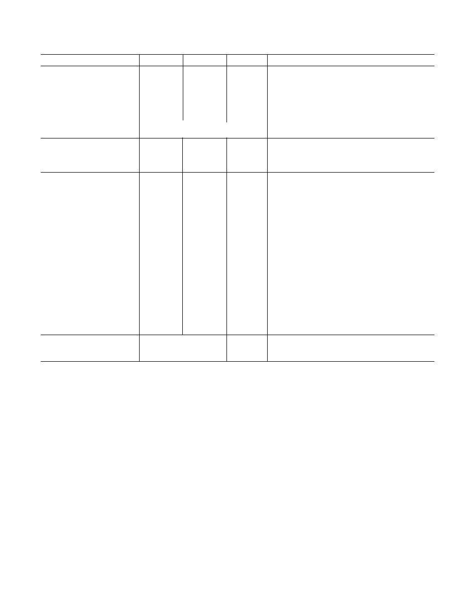
Parameter
A Version
1
B Version
1
Units
Test Conditions/Comments
DYNAMIC PERFORMANCE
Signal to Noise + Distortion Ratio
3
70
71
dB min
Typically SNR Is 72 dB
(SNR)
V
IN
= 10 kHz Sine Wave, f
SAMPLE
= 200 kHz (100 kHz)
Total Harmonic Distortion (THD)
≠78
≠78
dB max
V
IN
= 10 kHz Sine Wave, f
SAMPLE
= 200 kHz (100 kHz)
Peak Harmonic or Spurious Noise
≠78
≠78
dB max
V
IN
= 10 kHz Sine Wave, f
SAMPLE
= 200 kHz (100 kHz)
Intermodulation Distortion (IMD)
Second Order Terms
≠78
≠80
dB typ
fa = 9.983 kHz, fb = 10.05 kHz, f
SAMPLE
= 200 kHz (100 kHz)
Third Order Terms
≠78
≠80
dB typ
fa = 9.983 kHz, fb = 10.05 kHz, f
SAMPLE
= 200 kHz (100 kHz)
DC ACCURACY
Resolution
12
12
Bits
Integral Nonlinearity
±
1
±
1
LSB max
2.5 V External Reference V
DD
= 3 V, V
DD
= 5 V (B Grade Only)
±
1
±
0.5
LSB max
5 V External Reference V
DD
= 5 V
(
±
1)
LSB max
(L Version, 5 V External Reference, V
DD
= 5 V)
(
±
1)
LSB max
(L Version)
Differential Nonlinearity
±
1
±
1
LSB max
Guaranteed No Missed Codes to 12 Bits. 2.5 V External Reference
V
DD
= 3 V, 5 V External Reference V
DD
= 5 V
Total Unadjusted Error
±
1
±
1
LSB typ
Unipolar Offset Error
±
1
±
1
LSB max
2.5 V External Reference V
DD
= 3 V, 5 V External Reference V
DD
= 5 V
Unipolar Offset Error
(
±
2.5)
(
±
2.5)
LSB max
(L Versions, 2.5 V External Reference V
DD
= 3 V, 5 V External
Reference V
DD
= 5 V)
Positive Full-Scale Error
±
2.5
±
2.5
LSB max
2.5 V External Reference V
DD
= 3 V, 5 V External Reference V
DD
= 5 V
Positive Full-Scale Error
(
±
4)
(
±
4)
LSB max
(L Versions, 2.5 V External Reference V
DD
= 3 V, 5 V External
Reference V
DD
= 5 V)
Negative Full-Scale Error
±
2.5
±
2.5
LSB max
2.5 V External Reference V
DD
= 3 V, 5 V External Reference V
DD
= 5 V
Negative Full-Scale Error
(
±
4)
(
±
4)
LSB max
(L Versions, 2.5 V External Reference V
DD
= 3 V, 5 V External
Reference V
DD
= 5 V)
Bipolar Zero Error
±
2
±
2
LSB max
2.5 V External Reference V
DD
= 3 V, 5 V External Reference V
DD
= 5 V
Bipolar Zero Error
(
±
2.5)
(
±
2.5)
LSB max
(L Versions, 2.5 V External Reference V
DD
= 3 V, 5 V External
Reference V
DD
= 5 V)
ANALOG INPUT
Input Voltage Ranges
0 to V
REF
0 to V
REF
Volts
i.e., AIN(+) ≠ AIN(≠) = 0 to V
REF
, AIN(≠) Can Be Biased
Up But AIN(+) Cannot Go Below AIN(≠)
±
V
REF
/2
±
V
REF
/2
Volts
i.e., AIN(+) ≠ AIN(≠) = ≠V
REF
/2 to +V
REF
/2, AIN(≠) Should
Be Biased to +V
REF
/2 and AIN(+) Can Go Below AIN(≠) But
Cannot Go Below 0 V
Leakage Current
±
1
±
1
µ
A max
Input Capacitance
20
20
pF typ
REFERENCE INPUT/OUTPUT
REF
IN
Input Voltage Range
2.3/V
DD
2.3/V
DD
V min/max
Functional from 1.2 V
Input Impedance
150
150
k
typ
REF
OUT
Output Voltage
2.3/2.7
2.3/2.7
V min/max
REF
OUT
Tempco
20
20
ppm/
∞
C typ
LOGIC INPUTS
Input High Voltage, V
INH
2.4
2.4
V min
AV
DD
= DV
DD
= 4.5 V to 5.5 V
2.1
2.1
V min
AV
DD
= DV
DD
= 3.0 V to 3.6 V
Input Low Voltage, V
INL
0.8
0.8
V max
AV
DD
= DV
DD
= 4.5 V to 5.5 V
0.6
0.6
V max
AV
DD
= DV
DD
= 3.0 V to 3.6 V
Input Current, I
IN
±
10
±
10
µ
A max
Typically 10 nA, V
IN
= 0 V or V
DD
Input Capacitance, C
IN
4
10
10
pF max
AD7853/AD7853L≠SPECIFICATIONS
1, 2
REV. B
≠2≠
(AV
DD
= DV
DD
= +3.0 V to +5.5 V, REF
IN
/REF
OUT
= 2.5 V
External Reference, f
CLKIN
= 4 MHz (1.8 MHz B Grade (0 C to +70 C), 1 MHz A and B Grades (≠40 C to +85 C) for L Version); f
SAMPLE
= 200 kHz
(AD7853) 100 kHz (AD7853L);
SLEEP = Logic High; T
A
= T
MIN
to T
MAX
, unless otherwise noted.) Specifications in () apply to the AD7853L.
Parameter
A Version
1
B Version
1
Units
Test Conditions/Comments
LOGIC OUTPUTS
Output High Voltage, V
OH
I
SOURCE
= 200
µ
A
4
4
V min
AV
DD
= DV
DD
= 4.5 V to 5.5 V
2.4
2.4
V min
AV
DD
= DV
DD
= 3.0 V to 3.6 V
Output Low Voltage, V
OL
0.4
0.4
V max
I
SINK
= 0.8 mA
Floating-State Leakage Current
±
10
±
10
µ
A max
Floating-State Output Capacitance
4
10
10
pF max
Output Coding
Straight (Natural) Binary
Unipolar Input Range
Twos Complement
Bipolar Input Range
CONVERSION RATE
Conversion Time
4.6 (18)
4.6 (18)
µ
s max
(L Versions Only, ≠40
∞
C to +85
∞
C, 1 MHz CLKIN)
(10)
µ
s max
(L Versions Only, 0
∞
C to +70
∞
C, 1.8 MHz CLKIN)
Track/Hold Acquisition Time
0.4 (1)
0.4 (1)
µ
s min
(L Versions Only)
POWER REQUIREMENTS
AV
DD,
DV
DD
+3.0/+5.5
+3.0/+5.5
V min/max
I
DD
Normal Mode
5
6 (1.9)
6 (1.9)
mA max
AV
DD
= DV
DD
= 4.5 V to 5.5 V. Typically 4.5 mA (1.5);
5.5 (1.9)
5.5 (1.9)
mA max
AV
DD
= DV
DD
= 3.0 V to 3.6 V. Typically 4.0 mA (1.5 mA)
Sleep Mode
6
With External Clock On
10
10
µ
A typ
Full Power-Down. Power Management Bits in Control Register
Set as PMGT1 = 1, PMGT0 = 0
400
400
µ
A typ
Partial Power-Down. Power Management Bits in Control
Register Set as PMGT1 = 1, PMGT0 = 1
With External Clock Off
5
5
µ
A max
Typically 1
µ
A. Full-Power Down. Power Management Bits in
Control Register Set as PMGT1 = 1, PMGT0 = 0
200
200
µ
A typ
Partial Power-Down. Power Management Bits in Control
Register Set as PMGT1 = 1, PMGT0 = 1
Normal Mode Power Dissipation
33 (10.5)
33 (10.5)
mW max
V
DD
= 5.5 V: Typically 25 mW (8);
SLEEP = V
DD
20 (6.85)
20 (6.85)
mW max
V
DD
= 3.6 V: Typically 15 mW (5.4);
SLEEP = V
DD
Sleep Mode Power Dissipation
With External Clock On
55
55
µ
W typ
V
DD
= 5.5 V;
SLEEP = 0 V
36
36
µ
W typ
V
DD
= 3.6 V;
SLEEP = 0 V
With External Clock Off
27.5
27.5
µ
W max
V
DD
= 5.5 V: Typically 5.5
µ
W;
SLEEP = 0 V
18
18
µ
W max
V
DD
= 3.6 V: Typically 3.6
µ
W;
SLEEP = 0 V
SYSTEM CALIBRATION
Offset Calibration Span
7
+0.05
◊
V
REF
/≠0.05
◊
V
REF
V max/min
Allowable Offset Voltage Span for Calibration
Gain Calibration Span
7
+1.025
◊
V
REF
/≠0.975
◊
V
REF
V max/min
Allowable Full-Scale Voltage Span for Calibration
NOTES
1
Temperature ranges as follows: A, B Versions, ≠40
∞
C to +85
∞
C. For L Versions, A and B Versions f
CLKIN
= 1 MHz over ≠40
∞
C to +85
∞
C temperature range,
B Version f
CLKIN
= 1.8 MHz over 0
∞
C to +70
∞
C temperature range.
2
Specifications apply after calibration.
3
SNR calculation includes distortion and noise components.
4
Sample tested @ +25
∞
C to ensure compliance.
5
All digital inputs @ DGND except for
CONVST, SLEEP, CAL, and SYNC @ DV
DD
. No load on the digital outputs. Analog inputs @ AGND.
6
CLKIN @ DGND when external clock off. All digital inputs @ DGND except for
CONVST, SLEEP, CAL, and SYNC @ DV
DD
. No load on the digital outputs.
Analog inputs @ AGND.
7
The offset and gain calibration spans are defined as the range of offset and gain errors that the AD7853/AD7853L can calibrate. Note also that these are voltage spans
and are not absolute voltages (i.e., the allowable system offset voltage presented at AIN(+) for the system offset error to be adjusted out will be AIN(≠)
±
0.05
◊
V
REF
,
and the allowable system full-scale voltage applied between AIN(+) and AIN(≠) for the system full-scale voltage error to be adjusted out will be V
REF
±
0.025
◊
V
REF
).
This is explained in more detail in the calibration section of the data sheet.
Specifications subject to change without notice.
AD7853/AD7853L
REV. B
≠3≠

REV. B
≠4≠
AD7853/AD7853L
TIMING SPECIFICATIONS
1
Limit at T
MIN
, T
MAX
(A, B Versions)
Parameter
5 V
3 V
Units
Description
f
CLKIN
2
500
500
kHz min
Master Clock Frequency
4
4
MHz max
1.8
1.8
MHz max
L Version, 0
∞
C to +70
∞
C, B Grade Only
1
1
MHz max
L Version, ≠40
∞
C to +85
∞
C
f
SCLK
3
4
4
MHz max
Interface Modes 1, 2, 3 (External Serial Clock)
f
CLKIN
f
CLKIN
MHz max
Interface Modes 4, 5 (Internal Serial Clock)
t
1
4
100
100
ns min
CONVST Pulsewidth
t
2
50
90
ns max
CONVST
to BUSY
Propagation Delay
t
CONVERT
4.6
4.6
µ
s max
Conversion Time = 18 t
CLKIN
10 (18)
10 (18)
µ
s max
L Version 1.8 (1) MHz CLKIN. Conversion Time = 18 t
CLKIN
t
3
≠0.4 t
SCLK
≠0.4 t
SCLK
ns min
SYNC
to SCLK
Setup Time (Noncontinuous SCLK Input)
0.4 t
SCLK
0.4 t
SCLK
ns min/max
SYNC
to SCLK
Setup Time (Continuous SCLK Input)
t
4
0.6 t
SCLK
0.6 t
SCLK
ns min
SYNC
to SCLK
Setup Time. Interface Mode 4 Only
t
5
5
50
90
ns max
Delay from
SYNC
until DOUT 3-State Disabled
t
5A
5
50
90
ns max
Delay from
SYNC
until DIN 3-State Disabled
t
6
5
75
115
ns max
Data Access Time After SCLK
t
7
40
60
ns min
Data Setup Time Prior to SCLK
t
8
20
30
ns min
Data Valid to SCLK Hold Time
t
9
6
0.4 t
SCLK
0.4 t
SCLK
ns min
SCLK High Pulsewidth (Interface Modes 4 and 5)
t
10
6
0.4 t
SCLK
0.4 t
SCLK
ns min
SCLK Low Pulsewidth (Interface Modes 4 and 5)
t
11
30
50
ns min
SCLK
to
SYNC
Hold Time (Noncontinuous SCLK)
30/0.4 t
SCLK
50/0.4 t
SCLK
ns min/max
(Continuous SCLK) Does Not Apply to Interface Mode 3
t
11A
50
50
ns max
SCLK
to
SYNC
Hold Time
t
12
7
50
50
ns max
Delay from
SYNC
until DOUT 3-State Enabled
t
13
90
130
ns max
Delay from SCLK
to DIN Being Configured as Output
t
14
8
50
90
ns max
Delay from SCLK
to DIN Being Configured as Input
t
15
2.5 t
CLKIN
2.5 t
CLKIN
ns max
CAL
to BUSY
Delay
t
16
2.5 t
CLKIN
2.5 t
CLKIN
ns max
CONVST
to BUSY
Delay in Calibration Sequence
t
CAL
9
31.25
31.25
ms typ
Full Self-Calibration Time, Master Clock Dependent
(125013 t
CLKIN
)
t
CAL1
9
27.78
27.78
ms typ
Internal DAC Plus System Full-Scale Cal Time, Master Clock
Dependent (111114 t
CLKIN
)
t
CAL2
9
3.47
3.47
ms typ
System Offset Calibration Time, Master Clock Dependent
(13899 t
CLKIN
)
NOTES
Descriptions that refer to SCLK
(rising) or SCLK
(falling) edges here are with the POLARITY pin HIGH. For the POLARITY pin LOW then the opposite edge of
SCLK will apply.
1
Sample tested at +25
∞
C to ensure compliance. All input signals are specified with tr = tf = 5 ns (10% to 90% of V
DD
) and timed from a voltage level of 1.6 V. See
Table X and timing diagrams for different interface modes and calibration.
2
Mark/Space ratio for the master clock input is 40/60 to 60/40.
3
For Interface Modes 1, 2, 3 the SCLK max frequency will be 4 MHz. For Interface Modes 4 and 5 the SCLK will be an output and the frequency will be f
CLKIN
.
4
The
CONVST pulsewidth will apply here only for normal operation. When the part is in power-down mode, a different CONVST pulsewidth will apply (see Power-
Down section).
5
Measured with the load circuit of Figure 1 and defined as the time required for the output to cross 0.8 V or 2.4 V.
6
For self-clocking mode (Interface Modes 4, 5) the nominal SCLK high and low times will be 0.5 t
SCLK
= 0.5 t
CLKIN
.
7
t
12
is derived form the measured time taken by the data outputs to change 0.5 V when loaded with the circuit of Figure 1. The measured number is then extrapolated
back to remove the effects of charging or discharging the 100 pF capacitor. This means that the time, t
12
, quoted in the timing characteristics is the true bus relin-
quish time of the part and is independent of the bus loading.
8
t
14
is derived form the measured time taken by the data outputs to change 0.5 V when loaded with the circuit of Figure 1. The measured number is then extrapolated
back to remove the effects of charging or discharging the 100 pF capacitor. This means that the time quoted in the timing characteristics is the true delay of the part
in turning off the output drivers and configuring the DIN line as an input. Once this time has elapsed the user can drive the DIN line knowing that a bus conflict will
not occur.
9
The typical time specified for the calibration times is for a master clock of 4 MHz. For the L version the calibration times will be longer than those quoted here due to
the 1.8/1 MHz master clock.
Specifications subject to change without notice.
(AV
DD
= DV
DD
= +3.0 V to +5.5 V; f
CLKIN
= 4 MHz for AD7853 and 1.8/1 MHz for AD7853L; T
A
= T
MIN
to
T
MAX
, unless otherwise noted)
REV. B
≠5≠
AD7853/AD7853L
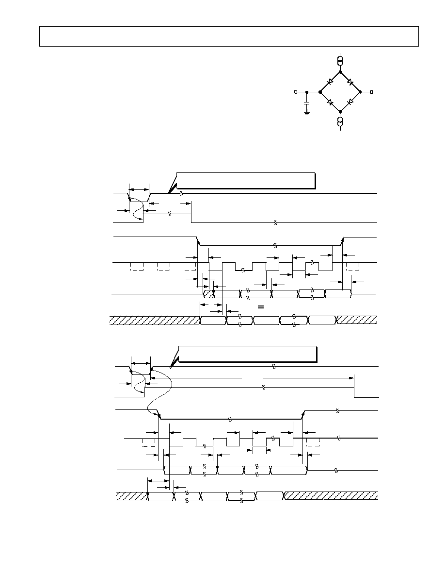
TYPICAL TIMING DIAGRAMS
Figures 2 and 3 show typical read and write timing diagrams.
Figure 2 shows the reading and writing after conversion in In-
terface Modes 2 and 3. To attain the maximum sample rate of
100 kHz (AD7853L) or 200 kHz (AD7853) in Interface Modes
2 and 3, reading and writing must be performed during conver-
sion. Figure 3 shows the timing diagram for Interface Modes 4
and 5 with sample rate of 100 kHz (AD7853L) or 200 kHz
(AD7853). At least 400 ns acquisition time must be allowed
(the time from the falling edge of BUSY to the next rising edge
of
CONVST) before the next conversion begins to ensure that
the part is settled to the 12-bit level. If the user does not want to
provide the
CONVST signal, the conversion can be initiated in
software by writing to the control register.
TO OUTPUT
PIN
+2.1V
I
OH
1.6mA
200 A
I
OL
C
L
100pF
Figure 1. Load Circuit for Digital Output Timing
Specifications
POLARITY PIN LOGIC HIGH
SYNC
(I/P)
SCLK (I/P)
t
3
BUSY (O/P)
CONVST
(I/P)
t
2
t
1
t
5
t
11
t
6
t
9
t
10
1
5
6
16
t
12
t
6
DOUT (O/P)
DB0
DB11
t
8
DB15
DB0
THREE-
STATE
DB11
THREE-
STATE
DB15
t
CONVERT
t
7
t
CONVERT
= 4.6 s MAX, 10 s FOR L VERSION
t
1
= 100 ns MIN,
t
5
= 50/90 ns MAX 5V/3V,
t
7
= 40/60 ns MIN 5V/3V
Figure 2. AD7853/AD7853L Timing Diagram (Typical Read and Write Operation for Interface Modes 2, 3)
POLARITY PIN LOGIC HIGH
SYNC
(O/P)
DOUT (O/P)
SCLK (O/P)
DB0
DB11
t
4
t
8
DIN (I/P)
DB15
DB0
THREE-
STATE
BUSY (O/P)
CONVST
(I/P)
DB11
t
2
t
1
t
7
t
11
t
6
t
9
t
10
THREE-
STATE
1
5
6
16
t
12
t
5
DB15
t
CONVERT
t
CONVERT
= 4.6 s MAX, 10 s FOR L VERSION
t
1
= 100 ns MIN,
t
5
= 50/90 ns MAX 5V/3V,
t
7
= 40/60 ns MIN 5V/3V
Figure 3. AD7853/AD7853L Timing Diagram (Typical Read and Write Operation for Interface Modes 4, 5)
REV. B
≠6≠
AD7853/AD7853L
ABSOLUTE MAXIMUM RATINGS
1
(T
A
= +25
∞
C unless otherwise noted)
AV
DD
to AGND . . . . . . . . . . . . . . . . . . . . . . . ≠0.3 V to +7 V
DV
DD
to DGND . . . . . . . . . . . . . . . . . . . . . . . ≠0.3 V to +7 V
AV
DD
to DV
DD
. . . . . . . . . . . . . . . . . . . . . . . ≠0.3 V to +0.3 V
Analog Input Voltage to AGND . . . . ≠0.3 V to AV
DD
+ 0.3 V
Digital Input Voltage to DGND . . . . ≠0.3 V to DV
DD
+ 0.3 V
Digital Output Voltage to DGND . . . ≠0.3 V to DV
DD
+ 0.3 V
REF
IN
/REF
OUT
to AGND . . . . . . . . . ≠0.3 V to AV
DD
+ 0.3 V
Input Current to Any Pin Except Supplies
2
. . . . . . . .
±
10 mA
Operating Temperature Range
Commercial (A, B Versions) . . . . . . . . . . . ≠40
∞
C to +85
∞
C
Storage Temperature Range . . . . . . . . . . . ≠65
∞
C to +150
∞
C
Junction Temperature . . . . . . . . . . . . . . . . . . . . . . . . . +150
∞
C
Plastic DIP Package, Power Dissipation . . . . . . . . . . 450 mW
JA
Thermal Impedance . . . . . . . . . . . . . . . . . . . . . 105
∞
C/W
JC
Thermal Impedance . . . . . . . . . . . . . . . . . . . . 34.7
∞
C/W
Lead Temperature, (Soldering, 10 sec) . . . . . . . . . . +260
∞
C
SOIC, SSOP Package, Power Dissipation . . . . . . . . . 450 mW
JA
Thermal Impedance . . . 75
∞
C/W (SOIC) 115
∞
C/W (SSOP)
JC
Thermal Impedance . . . . 25
∞
C/W (SOIC) 35
∞
C/W (SSOP)
Lead Temperature, Soldering
Vapor Phase (60 sec) . . . . . . . . . . . . . . . . . . . . . . +215
∞
C
Infrared (15 sec) . . . . . . . . . . . . . . . . . . . . . . . . . . +220
∞
C
ESD . . . . . . . . . . . . . . . . . . . . . . . . . . . . . . . . . . . . . . . . >3 kV
NOTES
1
Stresses above those listed under Absolute Maximum Ratings may cause perma-
nent damage to the device. This is a stress rating only; functional operation of the
device at these or any other conditions above those listed in the operational
sections of this specification is not implied. Exposure to absolute maximum rating
conditions for extended periods may affect device reliability.
2
Transient currents of up to 100 mA will not cause SCR latch-up.
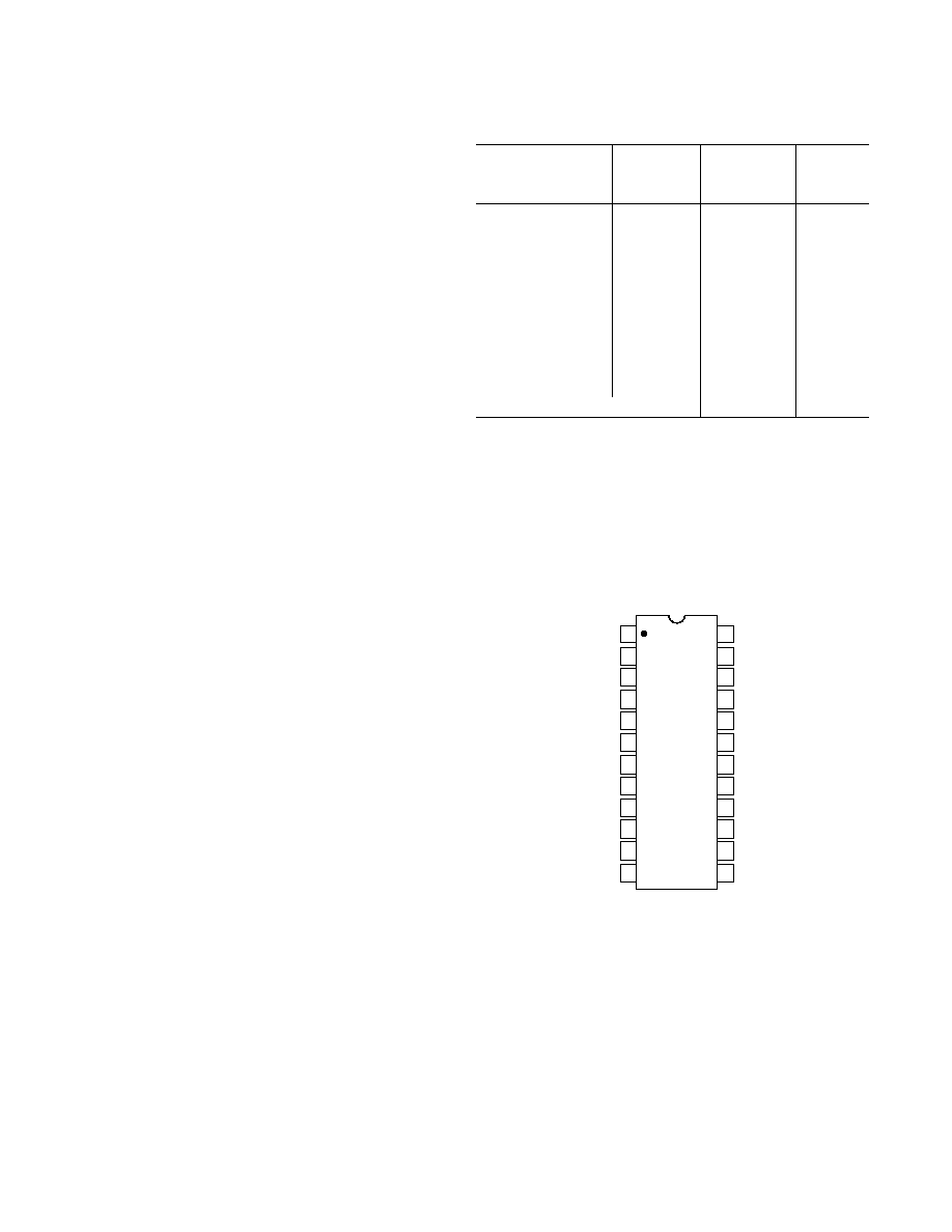
ORDERING GUIDE
Linearity
Power
Error
Dissipation
Package
Model
(LSB)
1
(mW)
Options
2
AD7853AN
±
1
20
N-24
AD7853BN
±
1/2
20
N-24
AD7853LAN
3
±
1
6.85
N-24
AD7853LBN
3
±
1
6.85
N-24
AD7853AR
±
1
20
R-24
AD7853BR
±
1/2
20
R-24
AD7853LAR
3
±
1
6.85
R-24
AD7853LBR
3
±
1
6.85
R-24
AD7853ARS
±
1
6.85
RS-24
AD7853LARS
3
±
1
6.85
RS-24
EVAL-AD7853CB
4
EVAL-CONTROL BOARD
5
NOTES
1
Linearity error refers to the integral linearity error.
2
N = Plastic DIP; R = SOIC; RS = SSOP.
3
L signifies the low power version.
4
This can be used as a stand-alone evaluation board or in conjunction with the
EVAL-CONTROL BOARD for evaluation/demonstration purposes.
5
This board is a complete unit allowing a PC to control and communicate with
all Analog Devices, Inc. evaluation boards ending in the CB designators.
PIN CONFIGURATIONS
DIP, SOIC AND SSOP
CAL
SCLK
SM2
SLEEP
REF
I N
/REF
OUT
BUSY
AIN(+)
AV
DD
AGND
CREF1
CREF2
AIN(≠)
CONVST
DV
DD
SYNC
1
2
3
7
24
23
22
21
20
19
18
17
16
15
14
13
8
9
10
11
12
4
5
6
CLKIN
DIN
DOUT
DGND
AMODE
POLARITY
SM1
NC
AGND
NC = NO CONNECT
TOP VIEW
(Not to Scale)
AD7853/53L
REV. B
≠7≠
AD7853/AD7853L
PIN FUNCTION DESCRIPTIONS
Pin
Mnemonic
Description
1
CONVST
Convert Start. Logic Input. A low to high transition on this input puts the track/hold into its hold mode and
starts conversion. When this input is not used, it should be tied to DV
DD
.
2
BUSY
Busy Output. The busy output is triggered high by the falling edge of
CONVST or rising edge of CAL, and
remains high until conversion is completed. BUSY is also used to indicate when the AD7853/AD7853L has
completed its on-chip calibration sequence.
3
SLEEP
Sleep Input/Low Power Mode. A Logic 0 initiates a sleep and all circuitry is powered down including the
internal voltage reference provided there is no conversion or calibration being performed. Calibration data
is retained. A Logic 1 results in normal operation. See Power-Down section for more details.
4
REF
IN
/
Reference Input/Output. This pin is connected to the internal reference through a series resistor and is the
REF
OUT
reference source for the analog-to-digital converter. The nominal reference voltage is 2.5 V and this appears
at the pin. This pin can be overdriven by an external reference or can be taken as high as AV
DD
. When this
pin is tied to AV
DD
, or when an externally applied reference approaches AV
DD
, the C
REF1
pin should also be
tied to AV
DD
.
5
AV
DD
Analog Positive Supply Voltage, +3.0 V to +5.5 V.
6, 12 AGND
Analog Ground. Ground reference for track/hold, reference and DAC.
7
C
REF1
Reference Capacitor (0.1
µ
F multilayer ceramic). This external capacitor is used as a charge source for the
internal DAC. The capacitor should be tied between the pin and AGND.
8
C
REF2
Reference Capacitor (0.01
µ
F ceramic disc). This external capacitor is used in conjunction with the on-chip
reference. The capacitor should be tied between the pin and AGND.
9
AIN(+)
Analog Input. Positive input of the pseudo-differential analog input. Cannot go below AGND or above
AV
DD
at any time, and cannot go below AIN(≠) when the unipolar input range is selected.
10
AIN(≠)
Analog Input. Negative input of the pseudo-differential analog input. Cannot go below AGND or above
AV
DD
at any time.
11
NC
No Connect Pin.
13
AMODE
Analog Mode Pin. This pin allows two different analog input ranges to be selected. A Logic 0 selects range
0 to V
REF
(i.e., AIN(+) ≠ AIN(≠) = 0 to V
REF
). In this case AIN(+) cannot go below AIN(≠) and
AIN(≠) cannot go below AGND. A Logic 1 selects range ≠V
REF
/2 to +V
REF
/2 (i.e., AIN(+) ≠ AIN(≠) =
≠V
REF
/2 to +V
REF
/2). In this case AIN(+) cannot go below AGND so that AIN(≠) needs to be biased to
+V
REF
/2 to allow AIN(+) to go from 0 V to +V
REF
V.
14
POLARITY
Serial Clock Polarity. This pin determines the active edge of the serial clock (SCLK). Toggling this pin will
reverse the active edge of the serial clock (SCLK). A Logic 1 means that the serial clock (SCLK) idles high
and a Logic 0 means that the serial clock (SCLK) idles low. It is best to refer to the timing diagrams and
Table IX for the SCLK active edges.
15
SM1
Serial Mode Select Pin. This pin is used in conjunction with the SM2 pin to give different modes of opera-
tion as described in Table X.
16
SM2
Serial Mode Select Pin. This pin is used in conjunction with the SM1 pin to give different modes of opera-
tion as described in Table X.
17
CAL
Calibration Input. This pin has an internal pull-up current source of 0.15
µ
A. A Logic 0 on this pin resets
all calibration control logic and initiates a calibration on its rising edge. There is the option of connecting a
10 nF capacitor from this pin to DGND to allow for an automatic self-calibration on power-up. This input
overrides all other internal operations. If the autocalibration is not required, this pin should be tied to a
logic high.
18
DV
DD
Digital Supply Voltage, +3.0 V to +5.5 V.
19
DGND
Digital Ground. Ground reference point for digital circuitry.
20
DOUT
Serial Data Output. The data output is supplied to this pin as a 16-bit serial word.
21
DIN
Serial Data Input. The data to be written is applied to this pin in serial form (16-bit word). This pin can act
as an input pin or as a I/O pin depending on the serial interface mode the part is in (see Table X).
22
CLKIN
Master Clock Signal for the device (4 MHz for AD7853, 1.8 MHz for AD7853L). Sets the conversion and
calibration times.
23
SCLK
Serial Port Clock. Logic input/output. The SCLK pin is configured as an input or output, dependent on the
type of serial data transmission (self-clocking or external-clocking) that has been selected by the SM1 and
SM2 pins. The SCLK idles high or low depending on the state of the POLARITY pin.
24
SYNC
This pin can be an input level triggered active low (similar to a chip select in one case and to a frame sync
in the other) or an output (similar to a frame sync) pin depending on SM1, SM2 (see Table X).

REV. B
≠8≠
AD7853/AD7853L
Total Harmonic Distortion
Total harmonic distortion (THD) is the ratio of the rms sum of
harmonics to the fundamental. For the AD7853/AD7853L, it is
defined as:
THD (dB)
=
20 log
(V
2
2
+
V
3
2
+
V
4
2
+
V
5
2
+
V
6
2
)
V
1
where V
1
is the rms amplitude of the fundamental and V
2
, V
3
,
V
4
, V
5
and V
6
are the rms amplitudes of the second through the
sixth harmonics.
Peak Harmonic or Spurious Noise
Peak harmonic or spurious noise is defined as the ratio of the
rms value of the next largest component in the ADC output
spectrum (up to f
S
/2 and excluding dc) to the rms value of the
fundamental. Normally, the value of this specification is deter-
mined by the largest harmonic in the spectrum, but for parts
where the harmonics are buried in the noise floor, it will be a
noise peak.
Intermodulation Distortion
With inputs consisting of sine waves at two frequencies, fa and
fb, any active device with nonlinearities will create distortion
products at sum and difference frequencies of mfa
±
nfb where
m, n = 0, 1, 2, 3, etc. Intermodulation distortion terms are
those for which neither m nor n are equal to zero. For example,
the second order terms include (fa + fb) and (fa ≠ fb), while the
third order terms include (2fa + fb), (2fa ≠ fb), (fa + 2fb) and
(fa ≠ 2fb).
Testing is performed using the CCIF standard where two input
frequencies near the top end of the input bandwidth are used. In
this case, the second order terms are usually distanced in fre-
quency from the original sine waves while the third order terms
are usually at a frequency close to the input frequencies. As a
result, the second and third order terms are specified separately.
The calculation of the intermodulation distortion is as per the
THD specification where it is the ratio of the rms sum of the
individual distortion products to the rms amplitude of the sum
of the fundamentals expressed in dBs.
TERMINOLOGY
Integral Nonlinearity
This is the maximum deviation from a straight line passing
through the endpoints of the ADC transfer function. The end-
points of the transfer function are zero scale, a point 1/2 LSB
below the first code transition, and full scale, a point 1/2 LSB
above the last code transition.
Differential Nonlinearity
This is the difference between the measured and the ideal 1 LSB
change between any two adjacent codes in the ADC.
Total Unadjusted Error
This is the deviation of the actual code from the ideal code
taking all errors into account (Gain, Offset, Integral Nonlinearity,
and other errors) at any point along the transfer function.
Unipolar Offset Error
This is the deviation of the first code transition (00 . . . 000 to
00 . . . 001) from the ideal AIN(+) voltage (AIN(≠) + 1/2 LSB)
when operating in the unipolar mode.
Positive Full-Scale Error
This applies to the unipolar and bipolar modes and is the devia-
tion of the last code transition from the ideal AIN(+) voltage
(AIN(≠) + Full Scale ≠ 1.5 LSB) after the offset error has been
adjusted out.
Negative Full-Scale Error
This applies to the bipolar mode only and is the deviation of the
first code transition (10 . . . 000 to 10 . . . 001) from the ideal
AIN(+) voltage (AIN(≠) ≠ V
REF
/2 + 0.5 LSB).
Bipolar Zero Error
This is the deviation of the midscale transition (all 1s to all 0s)
from the ideal AIN(+) voltage (AIN(≠) ≠ 1/2 LSB).
Track/Hold Acquisition Time
The track/hold amplifier returns into track mode and the end of
conversion. Track/Hold acquisition time is the time required for
the output of the track/hold amplifier to reach its final value,
within
±
1/2 LSB, after the end of conversion.
Signal to (Noise + Distortion) Ratio
This is the measured ratio of signal to (noise + distortion) at the
output of the A/D converter. The signal is the rms amplitude of
the fundamental. Noise is the sum of all nonfundamental sig-
nals up to half the sampling frequency (f
S
/2), excluding dc. The
ratio is dependent on the number of quantization levels in the
digitization process; the more levels, the smaller the quantiza-
tion noise. The theoretical signal to (noise + distortion) ratio for
an ideal N-bit converter with a sine wave input is given by:
Signal to (Noise + Distortion) = (6.02 N +1.76) dB
Thus for a 12-bit converter, this is 74 dB.
REV. B
≠9≠
AD7853/AD7853L
ON-CHIP REGISTERS
The AD7853/AD7853L powers up with a set of default conditions, and the user need not ever write to the device. In this case the
AD7853/AD7853L will operate as a Read-Only ADC. The AD7853/AD7853L still retains the flexibility for performing a full power-
down, and a full self-calibration. Note that the DIN pin should be tied to DGND for operating the AD7853/AD7853L as a Read-
Only ADC.
Extra features and flexibility such as performing different power-down options, different types of calibrations including system cali-
bration, and software conversion start can be selected by writing to the part.
The AD7853/AD7853L contains a Control register, ADC output data register, Status register, Test register and 10 Calibra-
tion registers. The control register is write-only, the ADC output data register and the status register are read-only, and the test and
calibration registers are both read/write registers. The test register is used for testing the part and should not be written to.
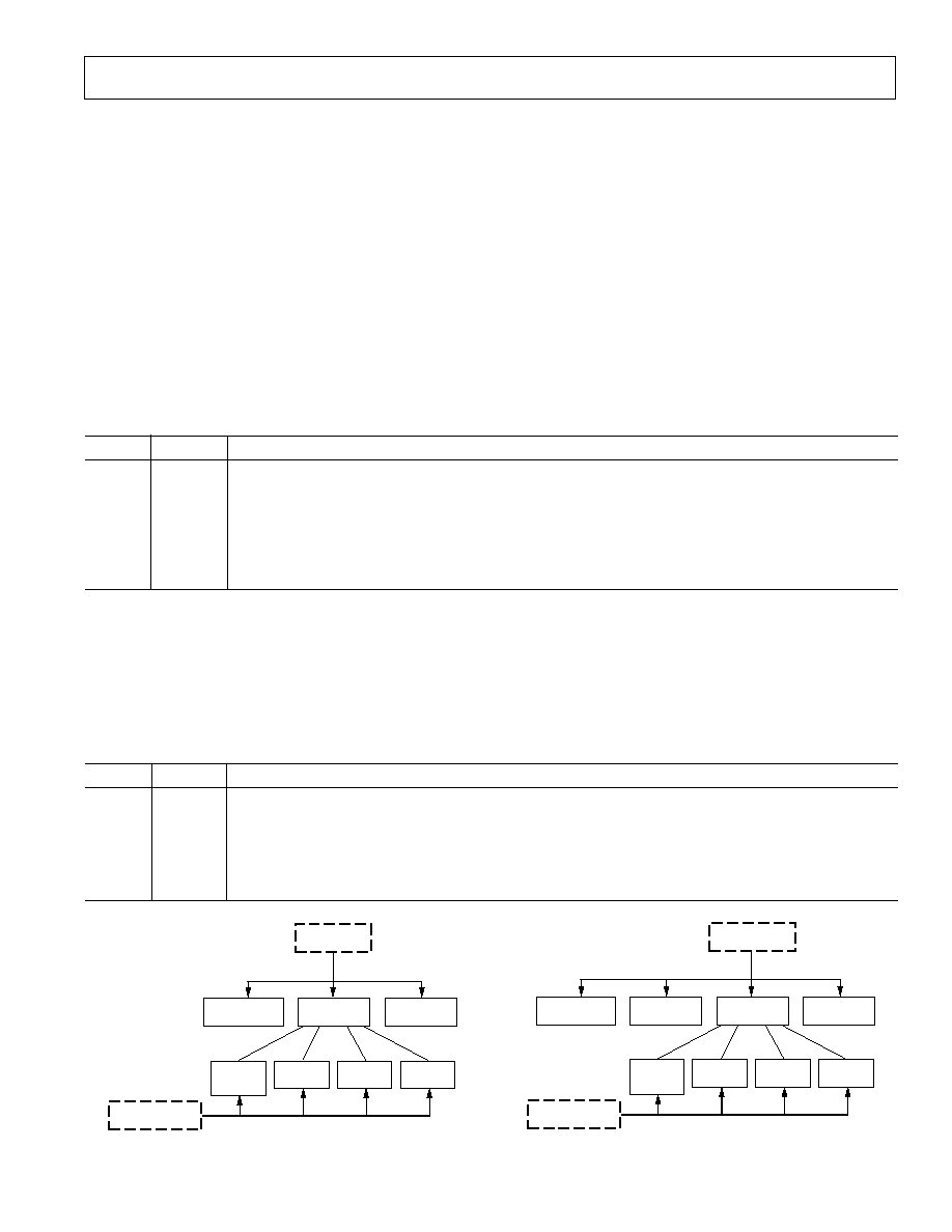
Addressing the On-Chip Registers
Writing
A write operation to the AD7853/AD7853L consists of 16 bits. The two MSBs, ADDR0 and ADDR1, are decoded to determine
which register is addressed, and the subsequent 14 bits of data are written to the addressed register. It is not until all 16 bits are writ-
ten that the data is latched into the addressed register. Table I shows the decoding of the address bits, while Figure 4 shows the over-
all write register hierarchy.
Table I. Write Register Addressing
ADDR1
ADDR0
Comment
0
0
This combination does not address any register so the subsequent 14 data bits are ignored.
0
1
This combination addresses the TEST REGISTER. The subsequent 14 data bits are written to the test register.
1
0
This combination addresses the CALIBRATION REGISTERS. The subsequent 14 data bits are written
to the selected calibration register.
1
1
This combination addresses the CONTROL REGISTER. The subsequent 14 data bits are written to the
control register.
Reading
To read from the various registers the user must first write to Bits 6 and 7 in the Control Register, RDSLT0 and RDSLT1. These
bits are decoded to determine which register is addressed during a read operation. Table II shows the decoding of the read address
bits while Figure 5 shows the overall read register hierarchy. The power-up status of these bits is 00 so that the default read will be
from the ADC output data register.
Once the read selection bits are set in the control register all subsequent read operations that follow will be from the selected register
until the read selection bits are changed in the control register.
Table II. Read Register Addressing
RDSLT1
RDSLT0
Comment
0
0
All successive read operations will be from ADC OUTPUT DATA REGISTER. This is the power-up
default setting. There will always be four leading zeros when reading from the ADC output data register.
0
1
All successive read operations will be from TEST REGISTER.
1
0
All successive read operations will be from CALIBRATION REGISTERS.
1
1
All successive read operations will be from STATUS REGISTER.
ADDR1, ADDR0
DECODE
CALIBRATION
REGISTERS
GAIN(1)
OFFSET(1)
01
10
11
CALSLT1, CALSLT0
DECODE
00
01
10
11
TEST
REGISTER
CONTROL
REGISTER
OFFSET(1)
GAIN(1)
GAIN(1)
OFFSET(1)
DAC(8)
Figure 4. Write Register Hierarchy/Address Decoding
RDSLT1, RDSLT0
DECODE
CALIBRATION
REGISTERS
GAIN(1)
OFFSET(1)
01
10
11
CALSLT1, CALSLT0
DECODE
00
01
10
11
TEST
REGISTER
STATUS
REGISTER
OFFSET(1)
GAIN(1)
GAIN(1)
OFFSET(1)
DAC(8)
ADC OUTPUT
DATA REGISTER
00
Figure 5. Read Register Hierarchy/Address Decoding
REV. B
≠10≠
AD7853/AD7853L
CONTROL REGISTER
The arrangement of the control register is shown below. The control register is a write only register and contains 14 bits of data. The
control register is selected by putting two 1s in ADDR1 and ADDR0. The function of the bits in the control register are described
below. The power-up status of all bits is 0.
MSB
ZERO
ZERO
ZERO
ZERO
PMGT1
PMGT0
RDSLT1
RDSLT0
2/
3 MODE
CONVST
CALMD
CALSLT1
CALSLT0
STCAL
LSB
Control Register Bit Function Descriptions
Bit
Mnemonic
Comment
13
ZERO
These four bits must be set to 0 when writing to the control register.
12
ZERO
11
ZERO
10
ZERO
9
PMGT1
Power Management Bits. These two bits are used with the
SLEEP pin for putting the part into various
8
PMGT0
power-down modes (See Power-Down section for more details).
7
RDSLT1
These two bits determine which register is addressed for the read operations. See Table II.
6
RDSLT0
5
2/
3 MODE
Interface Mode Select Bit. With this bit set to 0, Interface Mode 2 is enabled. With this bit set to 1,
Interface Mode 1 is enabled where DIN is used as an output as well as an input. This bit is set to 0 by
default after every read cycle; thus when using Interface Mode 1, this bit needs to be set to 1 in every
write cycle.
4
CONVST
Conversion Start Bit. A logic one in this bit position starts a single conversion, and this bit is automati-
cally reset to 0 at the end of conversion. This bit may also used in conjunction with system calibration
(see Calibration Section on page 21).
3
CALMD
Calibration Mode Bit. A 0 here selects self-calibration and a 1 selects a system calibration (see Table III).
2
CALSLT1
Calibration Selection Bits and Start Calibration Bit. These bits have two functions.
1
CALSLT0
With the STCAL bit set to 1, the CALSLT1 and CALSLT0 bits determine the type of calibration per-
0
STCAL
formed by the part (see Table III). The STCAL bit is automatically reset to 0 at the end of calibration.
With the STCAL bit set to 0, the CALSLT1 and CALSLT0 bits are decoded to address the calibration
register for read/write of calibration coefficients (see section on the calibration registers for more details).
Table III. Calibration Selection
CALMD
CALSLT1
CALSLT0
Calibration Type
0
0
0
A full internal calibration is initiated where the internal DAC is calibrated followed by the
internal gain error and finally the internal offset error is calibrated out. This is the default setting.
0
0
1
Here the internal gain error is calibrated out followed by the internal offset error calibrated
out.
0
1
0
This calibrates out the internal offset error only.
0
1
1
This calibrates out the internal gain error only.
1
0
0
A full system calibration is initiated here where first the internal DAC is calibrated, fol-
lowed by the system gain error, and finally the system offset error is calibrated out.
1
0
1
Here the system gain error is calibrated out followed by the system offset error.
1
1
0
This calibrates out the system offset error only.
1
1
1
This calibrates out the system gain error only.
REV. B
≠11≠
AD7853/AD7853L
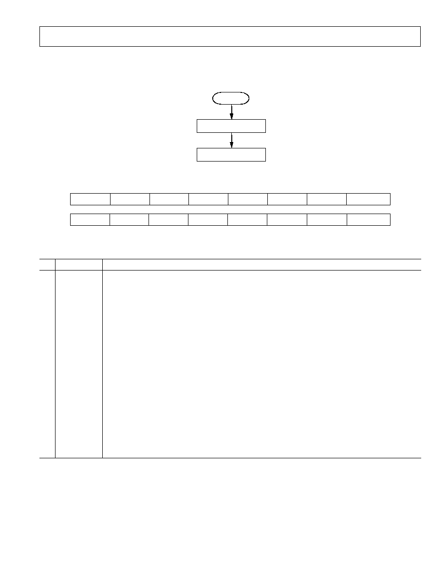
STATUS REGISTER
The arrangement of the status register is shown below. The status register is a read-only register and contains 16 bits of data. The
status register is selected by first writing to the control register and putting two 1s in RDSLT1 and RDSLT0. The function of the
bits in the status register are described below. The power-up status of all bits is 0.
WRITE TO CONTROL REGISTER
SETTING RDSLT0 = RDSLT1 = 1
START
READ STATUS REGISTER
Figure 6. Flowchart for Reading the Status Register
MSB
ZERO
BUSY
ZERO
ZERO
ZERO
ZERO
PMGT1
PMGT0
RDSLT1
RDSLT0
2/
3 MODE
X
CALMD
CALSLT1
CALSLT0
STCAL
LSB
Status Register Bit Function Descriptions
Bit
Mnemonic
Comment
15
ZERO
This bit is always 0.
14
BUSY
Conversion/Calibration Busy Bit. When this bit is 1, it indicates that there is a conversion or calibration in
progress. When this bit is 0, no conversion or calibration is in progress.
13
ZERO
These four bits are always 0.
12
ZERO
11
ZERO
10
ZERO
9
PMGT1
Power Management Bits. These bits, along with the
SLEEP pin, will indicate whether or not the part is in a
8
PMGT0
power-down mode. See Table VI in Power-Down Section for description.
7
RDSLT1
Both of these bits are always 1, indicating it is the status register that is being read. See Table II.
6
RDSLT0
5
2/
3 MODE
Interface Mode Select Bit. With this bit at 0, the device is in Interface Mode 2. With this bit at 1, the device
is in Interface Mode 1. This bit is reset to 0 after every read cycle.
4
X
Don't care bit.
3
CALMD
Calibration Mode Bit. A 0 in this bit indicates a self-calibration is selected; a 1 in this bit indicates a system
calibration is selected (see Table III).
2
CALSLT1
Calibration Selection Bits and Start Calibration Bit. The STCAL bit is read as a 1 if a calibration is in
1
CALSLT0
progress and as a 0 if no calibration is in progress. The CALSLT1 and CALSLT0 bits indicate
0
STCAL
which of the calibration registers are addressed for reading and writing (see section on the Calibration
Registers for more details).
REV. B
≠12≠
AD7853/AD7853L
CALIBRATION REGISTERS
The AD7853/AD7853L has ten calibration registers in all, eight for the DAC, one for the offset and one for gain. Data can be writ-
ten to or read from all ten calibration registers. In self- and system calibration the part automatically modifies the calibration regis-
ters; only if the user needs to modify the calibration registers should an attempt be made to read from and write to the calibration
registers.
Addressing the Calibration Registers
The calibration selection bits in the control register CALSLT1 and CALSLT0 determine which of the calibration registers are ad-
dressed (See Table IV). The addressing applies to both the read and write operations for the calibration registers. The user should
not attempt to read from and write to the calibration registers at the same time.
Table IV. Calibration Register Addressing
CALSLT1 CALSLT0
Comment
0
0
This combination addresses the Gain (1), Offset (1) and DAC Registers (8). Ten registers in total.
0
1
This combination addresses the Gain (1) and Offset (1) Registers. Two registers in total.
1
0
This combination addresses the Offset Register. One register in total.
1
1
This combination addresses the Gain Register. One register in total.
Writing to/Reading from the Calibration Registers
For writing to the calibration registers a write to the control
register is required to set the CALSLT0 and CALSLT1 bits.
For reading from the calibration registers a write to the control
register is required to set the CALSLT0 and CALSLT1 bits,
but also to set the RDSLT1 and RDSLT0 bits to 10 (this ad-
dresses the calibration registers for reading). The calibration
register pointer is reset on writing to the control register setting
the CALSLT1 and CALSLT0 bits, or upon completion of all
the calibration register write/read operations. When reset it
points to the first calibration register in the selected write/read
sequence. The calibration register pointer will point to the gain
calibration register upon reset in all but one case, this case
being where the offset calibration register is selected on its own
(CALSLT1 = 1, CALSLT0 = 0). Where more than one calibra-
tion register is being accessed, the calibration register pointer
will be automatically incremented after each calibration register
write/read operation. The order in which the ten calibration
registers are arranged is shown in Figure 7. The user may abort
at any time before all the calibration register write/read opera-
tions are completed, and the next control register write opera-
tion will reset the calibration register pointer. The flowchart in
Figure 8 shows the sequence for writing to the calibration regis-
ters and Figure 9 for reading.
GAIN REGISTER
OFFSET REGISTER
DAC 1st MSB REGISTER
DAC 8th MSB REGISTER
CAL REGISTER
ADDRESS POINTER
CALIBRATION REGISTERS
(1)
(2)
(3)
(10)
CALIBRATION REGISTER ADDRESS POINTER POSITION IS
DETERMINED BY THE NUMBER OF CALIBRATION REGISTERS
ADDRESSED AND THE NUMBER OF READ/WRITE OPERATIONS.
Figure 7. Calibration Register Arrangement
When reading from the calibration registers there will always be
two leading zeros for each of the registers. When operating in
serial Interface Mode 1, the read operations to the calibration
registers cannot be aborted. The full number of read operations
must be completed (see section on serial Interface Mode 1 tim-
ing for more detail).
WRITE TO CONTROL REGISTER SETTING STCAL = 0
AND CALSLT1, CALSLT0 = 00, 01, 10, 11
CAL REGISTER POINTER IS
AUTOMATICALLY RESET
FINISHED
NO
YES
START
WRITE TO CAL REGISTER
(ADDR1 = 1, ADDR0 = 0)
CAL REGISTER POINTER IS
AUTOMATICALLY INCREMENTED
LAST
REGISTER
WRITE
OPERATION
OR
ABORT
?
Figure 8. Flowchart for Writing to the Calibration Registers
REV. B
≠13≠
AD7853/AD7853L
WRITE TO CONTROL REGISTER SETTING STCAL = 0, RDSLT1 = 1,
RDSLT0 = 0, AND CALSLT1, CALSLT0 = 00, 01, 10, 11
CAL REGISTER POINTER IS
AUTOMATICALLY RESET
FINISHED
NO
YES
START
READ CAL REGISTER
CAL REGISTER POINTER IS
AUTOMATICALLY INCREMENTED
LAST
REGISTER
READ
OPERATION
OR
ABORT
?
Figure 9. Flowchart for Reading from the Calibration
Registers
Adjusting the Offset Calibration Register
The offset calibration register contains 16 bits, two leading zeros
and 14 data bits. By changing the contents of the offset register,
different amounts of offset on the analog input signal can be
compensated for. Increasing the number in the offset calibra-
tion register compensates for negative offset on the analog input
signal, and decreasing the number in the offset calibration regis-
ter compensates for positive offset on the analog input signal.
The default value of the offset calibration register is 0010 0000
0000 0000 approximately. This is not an exact value, but the
value in the offset register should be close to this value. Each of
the 14 data bits in the offset register is binary weighted; the
MSB has a weighting of 5% of the reference voltage, the MSB-1
has a weighting of 2.5%, the MSB-2 has a weighting of 1.25%,
and so on down to the LSB, which has a weighting of 0.0006%.
This gives a resolution of
±
0.0006% of V
REF
approximately.
More accurately the resolution is
±
(0.05
◊
V
REF
)/2
13
volts =
±
0.015 mV, with a 2.5 V reference. The maximum offset that
can be compensated for is
±
5% of the reference voltage, which
equates to
±
125 mV with a 2.5 V reference and
±
250 mV with a
5 V reference.
Q. If a +20 mV offset is present in the analog input signal and the
reference voltage is 2.5 V, what code needs to be written to the
offset register to compensate for the offset ?
A. 2.5 V reference implies that the resolution in the offset
register is 5%
◊
2.5 V/2
13
= 0.015 mV. +20 mV/0.015 mV
= 1310.72; rounding to the nearest number gives 1311. In
binary terms this is 0101 0001 1111, therefore decrease the
offset register by 0101 0001 1111.
This method of compensating for offset in the analog input
signal allows for fine tuning the offset compensation. If the
offset on the analog input signal is known, there will be no need
to apply the offset voltage to the analog input pins and do a
system calibration. The offset compensation can take place in
software.
Adjusting the Gain Calibration Register
The gain calibration register contains 16 bits, two leading 0s
and 14 data bits. The data bits are binary weighted as in the
offset calibration register. The gain register value is effectively
multiplied by the analog input to scale the conversion result
over the full range. Increasing the gain register compensates for
a smaller analog input range and decreasing the gain register
compensates for a larger input range. The maximum analog
input range that the gain register can compensate for is 1.025
times the reference voltage, and the minimum input range is
0.975 times
the reference voltage.
REV. B
≠14≠
AD7853/AD7853L
edge of
CONVST occurs at least 10 ns typically before this
CLKIN edge. The conversion cycle will take 16.5 CLKIN
periods from this CLKIN falling edge. If the 10 ns setup time is
not met, the conversion will take 17.5 CLKIN periods. The
maximum specified conversion time is 4.6
µ
s for the AD7853
(18 t
CLKIN,
CLKIN = 4 MHz) and 10
µ
s for the AD7853L (18
t
CLKIN
, CLKIN = 1.8 MHz). When a conversion is completed,
the BUSY output goes low, and then the result of the conver-
sion can be read by accessing the data through the serial inter-
face. To obtain optimum performance from the part, the read
operation should not occur during the conversion or 400 ns
prior to the next
CONVST rising edge. However, the maximum
throughput rates are achieved by reading/writing during conver-
sion, and reading/writing during conversion is likely to degrade
the Signal to (Noise + Distortion) by only 0.5 dBs. The AD7853
can operate at throughput rates up to 200 kHz, 100 kHz for
the AD7853L. For the AD7853/AD7853L a conversion takes
18 CLKIN periods, 2 CLKIN periods are needed for the
acquisition time giving a full cycle time of 5
µ
s (= 200 kHz,
CLKIN = 4 MHz). For the AD7853L 100 kHz throughput can
be obtained as follows: the CLKIN and
CONVST signals are
arranged to give a conversion time of 16.5 CLKIN periods as
described above, 1.5 CLKIN periods are allowed for the acqui-
sition time. This gives a full cycle time of 10
µ
s (= 100 kHz,
CLKIN = 1.8 MHz). When using the software conversion start
for maximum throughput, the user must ensure the control register
write operation extends beyond the falling edge of BUSY. The
falling edge of BUSY resets the
CONVST bit to 0 and allows it to
be reprogrammed to 1 to start the next conversion.
CIRCUIT INFORMATION
The AD7853/AD7853L is a fast, 12-bit single supply A/D con-
verter. The part requires an external 4 MHz/1.8 MHz master
clock (CLKIN), two C
REF
capacitors, a
CONVST signal to start
conversion and power supply decoupling capacitors. The part
provides the user with track/hold, on-chip reference, calibration
features, A/D converter and serial interface logic functions on a
single chip. The A/D converter section of the AD7853/AD7853L
consists of a conventional successive-approximation converter
based around a capacitor DAC. The AD7853/AD7853L accepts
an analog input range of 0 to +V
DD
where the reference can be
tied to V
DD
. The reference input to the part is buffered on-chip.
A major advantage of the AD7853/AD7853L is that a conver-
sion can be initiated in software as well as applying a signal to
the
CONVST pin. Another innovative feature of the AD7853/
AD7853L is self-calibration on power-up, which is initiated
having a capacitor from the
CAL pin to AGND, to give superior
dc accuracy (See Automatic Calibration on Power-Up section).
The part is available in a 24-lead SSOP package, which offers
the user considerable space-saving advantages over alternative
solutions. The AD7853L version typically consumes only 5.5 mW,
making it ideal for battery-powered applications.
CONVERTER DETAILS
The master clock for the part must be applied to the CLKIN
pin. Conversion is initiated on the AD7853/AD7853L by puls-
ing the
CONVST input or by writing to the control register and
setting the
CONVST bit to 1. On the rising edge of CONVST
(or at the end of the control register write operation), the on-
chip track/hold goes from track to hold mode. The falling edge
of the CLKIN signal which follows the rising edge of the edge of
CONVST signal initiates the conversion, provided the rising
AV
DD
DV
DD
AIN(+)
AIN(≠)
AMODE
C
REF1
C
REF2
SLEEP
DIN
DOUT
SYNC
SM1
SM2
CONVST
AGND
DGND
CLKIN
SCLK
REF
IN
/REF
OUT
POLARITY
AD7853/53L
ANALOG SUPPLY
+3V TO +5V
0.1 F
0.1 F
10 F
DV
DD
UNIPOLAR
RANGE
0.1 F
0.01 F
SERIAL MODE
SELECTION BITS
MASTER CLOCK INPUT
CONVERSION
START INPUT
FRAME SYNC OUTPUT
SERIAL DATA OUTPUT
0.1 F
CAL
AUTO CAL ON
POWER-UP
INTERNAL/EXTERNAL
REFERENCE
0V TO 2.5V
INPUT
4MHz/1.8MHz OSCILLATOR
SERIAL CLOCK OUTPUT
DV
DD
200kHz/100kHz PULSE
GENERATOR
CH1
CH2
CH3
CH4
OSCILLOSCOPE
OPTIONAL EXTERNAL
REFERENCE
AD780/REF-192
DIN AT DGND
=> NO WRITING
TO DEVICE
0.01 F
4 LEADING ZEROS
FOR ADC DATA
Figure 10. Typical Circuit
REV. B
≠15≠
AD7853/AD7853L
DC/AC Applications
For dc applications high source impedances are acceptable,
provided there is enough acquisition time between conversions
to charge the 20 pF capacitor. The acquisition time can be
calculated from the above formula for different source imped-
ances. For example with R
IN
= 5 k
, the required acquisition
time will be 922 ns.
For ac applications, removing high frequency components from
the analog input signal is recommended by use of an RC low-
pass filter on the AIN(+) pin, as shown in Figure 13. In applica-
tions where harmonic distortion and signal to noise ratio are
critical, the analog input should be driven from a low impedance
source. Large source impedances will significantly affect the ac
performance of the ADC. This may necessitate the use of an
input buffer amplifier. The choice of the op amp will be a func-
tion of the particular application.
When no amplifier is used to drive the analog input the source
impedance should be limited to low values. The maximum
source impedance will depend on the amount of total harmonic
distortion (THD) that can be tolerated. The THD will increase
as the source impedance increases and performance will degrade.
Figure 12 shows a graph of the Total Harmonic Distortion vs.
analog input signal frequency for different source impedances.
With the setup as in Figure 13, the THD is at the ≠90 dB level.
With a source impedance of 1 k
and no capacitor on the AIN(+)
pin, the THD increases with frequency.
INPUT FREQUENCY ≠ kHz
≠72
≠76
≠92
0
100
THD ≠ dB
20
40
60
80
≠80
≠84
≠88
R
IN
= 1k
R
IN
= 50 , 10nF
AS IN FIGURE 13
THD VS. FREQUENCY FOR DIFFERENT
SOURCE IMPEDANCES
Figure 12. THD vs. Analog Input Frequency
In a single supply application (both 3 V and 5 V), the V+ and
V≠ of the op amp can be taken directly from the supplies to the
AD7853/AD7853L which eliminates the need for extra external
power supplies. When operating with rail-to-rail inputs and
outputs at frequencies greater than 10 kHz, care must be taken
in selecting the particular op amp for the application. In particu-
lar, for single supply applications the input amplifiers should be
connected in a gain of ≠1 arrangement to get the optimum per-
formance. Figure 13 shows the arrangement for a single supply
application with a 50
and 10 nF low-pass filter (cutoff fre-
quency 320 kHz) on the AIN(+) pin. Note that the 10 nF is a
capacitor with good linearity to ensure good ac performance.
Recommended single supply op amps are the AD820 and the
AD820-3 V.
TYPICAL CONNECTION DIAGRAM
Figure 10 shows a typical connection diagram for the AD7853/
AD7853L. The DIN line is tied to DGND so that no data is
written to the part. The AGND and the DGND pins are con-
nected together at the device for good noise suppression. The
CAL pin has a 0.01
µ
F capacitor to enable an automatic self-
calibration on power-up. The SCLK and
SYNC are configured
as outputs by having SM1 and SM2 at DV
DD
. The conversion
result is output in a 16-bit word with four leading zeros followed
by the MSB of the 12-bit result. Note that after the AV
DD
and
DV
DD
power-up, the part will require approximately 150 ms for
the internal reference to settle and for the automatic calibration
on power-up to be completed.
For applications where power consumption is a major concern,
the
SLEEP pin can be connected to DGND. See Power-Down
section for more detail on low power applications.
ANALOG INPUT
The equivalent circuit of the analog input section is shown in
Figure 11. During the acquisition interval the switches are both
in the track position and the AIN(+) charges the 20 pF capaci-
tor through the 125
resistance. On the rising edge of
CONVST
switches SW1 and SW2 go into the hold position retaining
charge on the 20 pF capacitor as a sample of the signal on
AIN(+). The AIN(≠) is connected to the 20 pF capacitor, and
this unbalances the voltage at Node A at the input of the com-
parator. The capacitor DAC adjusts during the remainder of the
conversion cycle to restore the voltage at Node A to the correct
value. This action transfers a charge, representing the analog
input signal, to the capacitor DAC which in turn forms a digital
representation of the analog input signal. The voltage on the
AIN(≠) pin directly influences the charge transferred to the
capacitor DAC at the hold instant. If this voltage changes dur-
ing the conversion period, the DAC representation of the analog
input voltage will be altered. Therefore it is most important that
the voltage on the AIN(≠) pin remains constant during the con-
version period. Furthermore, it is recommended that the AIN(≠)
pin is always connected to AGND or to a fixed dc voltage.
AIN(+)
AIN(≠)
125
20pF
TRACK
HOLD
CAPACITOR
DAC
COMPARATOR
HOLD
TRACK
C
REF2
125
SW1
SW2
NODE A
Figure 11. Analog Input Equivalent Circuit
Acquisition Time
The track and hold amplifier enters its tracking mode on the
falling edge of the BUSY signal. The time required for the track
and hold amplifier to acquire an input signal will depend on
how quickly the 20 pF input capacitance is charged. The acqui-
sition time is calculated using the formula:
t
ACQ
= 9
◊
(R
IN
+ 125
)
◊
20 pF
where R
IN
is the source impedance of the input signal, and 125
,
20 pF is the input R, C.
REV. B
≠16≠
AD7853/AD7853L
AIN(+)
AIN(≠)
AMODE
AD7853/AD7853L
BIPOLAR
ANALOG
INPUT RANGE
SELECTED
DOUT
2S
COMPLEMENT
FORMAT
V
IN
= 0 TO V
REF
TRACK AND HOLD
AMPLIFIER
V
REF
/2
DV
DD
Figure 15.
±
V
REF
/2 about V
REF
/2 Bipolar Input Configuration
+FS ≠1LSB
OUTPUT
CODE
0V
111...111
111...110
111...101
111...100
000...011
000...001
000...000
000...010
V
IN
= (AIN(+) ≠ AIN(≠)), INPUT VOLTAGE
1LSB
1LSB =
FS
4096
Figure 16. Unipolar Transfer Characteristic
Figure 15 shows the AD7853/AD7853L's
±
V
REF
/2 bipolar ana-
log input configuration (where AIN(+) cannot go below 0 V so
for the full bipolar range then the AIN(≠) pin should be biased
to +V
REF
/2). Once again the designed code transitions occur
midway between successive integer LSB values. The output
coding is twos complement with 1 LSB = 4096 = 3.3 V/4096 =
0.8 mV. The ideal input/output transfer characteristic is shown
in Figure 17.
≠ 1 LSB
FS = V
REF
V
1LSB =
FS
4096
OUTPUT
CODE
V
REF
/2
011...111
011...110
000...001
000...000
100...001
100...000
100...010
V
IN
= (AIN(+) ≠ AIN(≠)), INPUT VOLTAGE
0V
+ FS
111...111
(V
REF
/2) ≠1 LSB
(V
REF
/2) +1 LSB
Figure 17. Bipolar Transfer Characteristic
IC1
AD820
AD820-3V
0.1 F
10 F
V+
V≠
10k
50
10nF
(NPO)
TO AIN(+) OF
AD7853/AD7853L
V
IN
≠V
REF
/2 TO +V
REF
/2
V
REF
/2
10k
10k
10k
+3V TO +5V
Figure 13. Analog Input Buffering
Input Ranges
The analog input range for the AD7853/AD7853L is 0 V to
V
REF
in both the unipolar and bipolar ranges.
The only difference between the unipolar range and the bipolar
range is that in the bipolar range the AIN(≠) has to be biased up
to +V
REF
/2 and the output coding is twos complement (See
Table V and Figures 14 and 15). The unipolar or bipolar mode
is selected by the AMODE pin (0 for the unipolar range and 1
for the bipolar range).
Table V. Analog Input Connections
Analog Input
Input Connections Connection
Range
AIN(+)
AIN(≠)
Diagram
AMODE
0 V to V
REF
1
V
IN
AGND
Figure 14
DGND
±
V
REF
/2
2
V
IN
V
REF
/2
Figure 15
DV
DD
NOTES
1
Output code format is straight binary.
2
Range is
±
V
REF
/2 biased about V
REF
/2. Output code format is twos complement.
Note that the AIN(≠) pin on the AD7853/AD7853L can be
biased up above AGND in the unipolar mode also, if required.
The advantage of biasing the lower end of the analog input
range away from AGND is that the user does not have to have
the analog input swing all the way down to AGND. This has the
advantage in true single supply applications that the input am-
plifier does not have to swing all the way down to AGND. The
upper end of the analog input range is shifted up by the same
amount. Care must be taken so that the bias applied does not
shift the upper end of the analog input above the AV
DD
supply.
In the case where the reference is the supply, AV
DD
, the AIN(≠)
must be tied to AGND in unipolar mode.
AIN(+)
AIN(≠)
AMODE
AD7853/AD7853L
UNIPOLAR ANALOG
INPUT RANGE
SELECTED
DOUT
STRAIGHT
BINARY
FORMAT
V
IN
= 0 TO V
REF
TRACK AND HOLD
AMPLIFIER
Figure 14. 0 to V
REF
Unipolar Input Configuration
Transfer Functions
For the unipolar range the designed code transitions occur
midway between successive integer LSB values (i.e., 1/2 LSB,
3/2 LSBs, 5/2 LSBs . . . FS ≠3/2 LSBs). The output coding is
straight binary for the unipolar range with 1 LSB = FS/4096 =
3.3 V/4096 = 0.8 mV when V
REF
= 3.3 V. The ideal input/output
transfer characteristic for the unipolar range is shown in
Figure 16.
REV. B
≠17≠
AD7853/AD7853L
REFERENCE SECTION
For specified performance, it is recommended that when using
an external reference this reference should be between 2.3 V
and the analog supply AV
DD
. The connections for the relevant
reference pins are shown in the typical connection diagrams. If
the internal reference is being used, the REF
IN
/REF
OUT
pin
should have a 100 nF capacitor connected to AGND very close
to the REF
IN
/REF
OUT
pin. These connections are shown in
Figure 18.
If the internal reference is required for use external to the ADC,
it should be buffered at the REF
IN
/REF
OUT
pin and a 100 nF
connected from this pin to AGND. The typical noise performance
for the internal reference, with 5 V supplies is 150 nV/
Hz @
1 kHz and dc noise is 100
µ
V p-p.
AV
DD
DV
DD
C
REF1
C
REF2
REF
IN
/REF
OUT
ANALOG SUPPLY
+3V TO +5V
0.1 F
10 F
0.1 F
0.01 F
0.1 F
0.1 F
AD7853/AD7853L
Figure 18. Relevant Connections When Using Internal
Reference
The other option is that the REF
IN
/REF
OUT
pin be overdriven
by connecting it to an external reference. This is possible due to
the series resistance from the REF
IN
/REF
OUT
pin to the internal
reference. This external reference can have a range that includes
AV
DD
. When using AV
DD
as the reference source, the 100 nF
capacitor from the REF
IN
/REF
OUT
pin to AGND should be as
close as possible to the REF
IN
/REF
OUT
pin, and also the C
REF1
pin should be connected to AV
DD
to keep this pin at the same
level as the reference. The connections for this arrangement are
shown in Figure 19. When using AV
DD
it may be necessary to
add a resistor in series with the AV
DD
supply. This will have the
effect of filtering the noise associated with the AV
DD
supply.
AV
DD
DV
DD
C
REF1
C
REF2
REF
IN
/REF
OUT
ANALOG SUPPLY
+3V TO +5V
0.1 F
10 F
0.1 F
0.01 F
0.1 F
0.1 F
AD7853/AD7853L
Figure 19. Relevant Connections When Using AV
DD
as the
Reference
PERFORMANCE CURVES
Figure 20 shows a typical FFT plot for the AD7853 at 200 kHz
sample rate and 10 kHz input frequency.
0
≠120
≠60
≠100
20
≠80
0
≠20
≠40
80
60
40
AV
DD
= DV
DD
= 3.3V
f
SAMPLE
= 200kHz
f
IN
= 10kHz
SNR = 72.04dB
THD = ≠88.43dB
FREQUENCY ≠ kHz
100
SNR ≠ dB
Figure 20. FFT Plot
Figure 21 shows the SNR versus Frequency for different sup-
plies and different external references.
INPUT FREQUENCY ≠ kHz
74
73
69
0
100
S(N+D) RATIO ≠ dB
20
40
60
80
72
71
70
5.0V SUPPLIES, WITH 5V REFERENCE
5.0V SUPPLIES
5.0V SUPPLIES, L VERSION
3.3V SUPPLIES
AV
DD
= DV
DD
WITH 2.5V REFERENCE
UNLESS STATED OTHERWISE
Figure 21. SNR vs. Frequency
Figure 22 shows the Power Supply Rejection Ratio versus Fre-
quency for the part. The Power Supply Rejection Ratio is de-
fined as the ratio of the power in ADC output at frequency f to
the power of a full-scale sine wave.
PSRR (dB) = 10 log (Pf/Pfs)
Pf = Power at frequency f in ADC output, Pfs = power of a full-
scale sine wave. Here a 100 mV peak-to-peak sine wave is
coupled onto the AV
DD
supply while the digital supply is left
unaltered. Both the 3.3 V and 5.0 V supply performances are
shown.
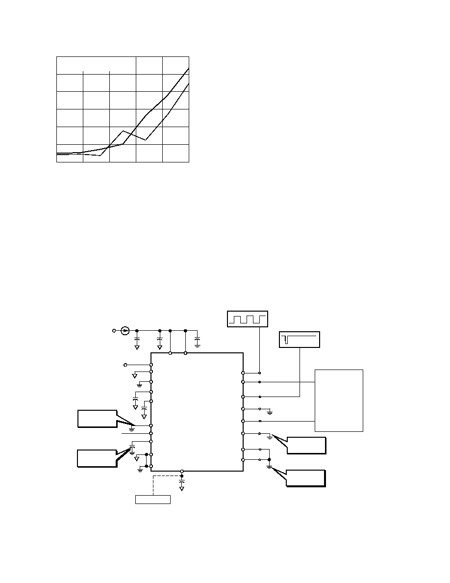
REV. B
≠18≠
AD7853/AD7853L
is powered down and I
DD
is 400
µ
A typ. The choice of full or par-
tial power-down does not give any significant improvement in
throughput with a power-down between conversions. This is
discussed in the next section≠Power-Up Times. However, a
partial power-down does allow the on-chip reference to be used
externally even though the rest of the AD7853 circuitry is pow-
ered down. It also allows the AD7853 to be powered up faster
after a long power-down period when using the on-chip refer-
ence (See Power-Up Times≠Using On-Chip Reference).
When using the
SLEEP pin, the power management bits PMGT1
and PMGT0 should be set to zero (default status on power-up).
Bringing the
SLEEP pin logic high ensures normal operation,
and the part does not power down at any stage. This may be
necessary if the part is being used at high throughput rates when
it is not possible to power down between conversions. If the user
wishes to power down between conversions at lower throughput
rates (i.e. <100 kSPS for the AD7853) to achieve better power
performances, then the
SLEEP pin should be tied logic low.
If the power-down options are to be selected in software only,
then the
SLEEP pin should be tied logic high. By setting the
power management bits PMGT1 and PMGT0 as shown in
Table VI, a Full Power-Down, Full Power-Up, Full Power-
Down Between Conversions, and a Partial Power-Down Be-
tween Conversions can be selected.
A typical connection diagram for a low power application is
shown in Figure 23 (AD7853L is the low power version of the
AD7853).
INPUT FREQUENCY ≠ kHz
≠78
≠80
≠90
0
100
PSRR ≠ dB
20
40
60
80
≠82
≠84
≠86
5.0V
3.3V
AV
DD
= DV
DD
= 3.3V/5.0V,
100mV p-p SINE WAVE ON AV
DD
≠88
Figure 22. PSRR vs. Frequency
POWER-DOWN OPTIONS
The AD7853 provides flexible power management to allow the
user to achieve the best power performance for a given through-
put rate. The power management options are selected by
programming the power management bits, PMGT1 and PMGT0,
in the control register and by use of the
SLEEP pin. Table VI
summarizes the power-down options that are available and how
they can be selected by using either software, hardware or a
combination of both. The AD7853 can be fully or partially
powered down. When fully powered down, all the on-chip cir-
cuitry is powered down and I
DD
is 1
µ
A typ. If a partial power-
down is selected, then all the on-chip circuitry except the reference
AV
DD
DV
DD
AIN(+)
AIN(≠)
AMODE
C
REF1
C
REF2
SLEEP
DIN
DOUT
SYNC
SM1
SM2
CONVST
AGND
DGND
CLKIN
SCLK
REF
IN
/REF
OUT
POLARITY
AD7853L
0.1 F
0.1 F
10 F
DV
DD
UNIPOLAR RANGE
0.1 F
0.01 F
SERIAL MODE
SELECTION BITS
MASTER CLOCK INPUT
CONVERSION
START INPUT
SERIAL DATA OUTPUT
0.1 F
CAL
0.01 F
INTERNAL
REFERENCE
0V TO 2.5V
INPUT
1.8MHz OSCILLATOR
SERIAL CLOCK INPUT
100kHz PULSE
GENERATOR
DIN AT DGND
=> NO WRITING
TO DEVICE
AUTO POWER-
DOWN AFTER
CONVERSION
THREE-WIRE
MODE
SELECTED
LOW POWER
C/ P
AUTO CAL ON
POWER-UP
CURRENT, I = 1.5mA TYP
REF-192
ANALOG SUPPLY
+3V
OPTIONAL EXTERNAL
REFERENCE
Figure 23. Typical Low Power Circuit
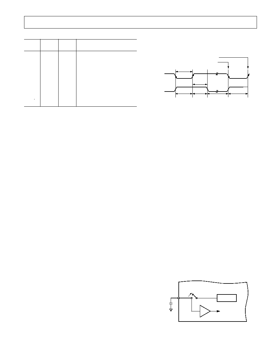
REV. B
≠19≠
AD7853/AD7853L
Table VI. Power Management Options
PMGT1 PMGT0
SLEEP
Bit
Bit
Pin
Comment
0
0
0
Full Power-Down if Not Cali-
brating or Converting (Default
Condition After Power-On)
0
0
1
Normal Operation
0
1
X
Normal Operation
(Independent of the
SLEEP Pin)
1
0
X
Full Power-Down
1
1
X
Partial Power-Down if Not
Converting
POWER-UP TIMES
Using an External Reference
When the AD7853 is powered up, the part is powered up from
one of two conditions. First, when the power supplies are ini-
tially powered up and, secondly, when the part is powered up
from either a hardware or software power-down (see last section).
When AV
DD
and DV
DD
are powered up, the AD7853 should be
left idle for approximately 32 ms (4 MHz CLK) to allow for the
autocalibration if a 10 nF cap is placed on the
CAL pin, (see
Calibration section). During power-up the functionality of the
SLEEP pin is disabled, i.e., the part will not power down until
the end of the calibration if
SLEEP is tied logic low. The auto-
calibration on power-up can be disabled if the
CAL pin is tied to
a logic high. If the autocalibration is disabled, then the user must
take into account the time required by the AD7853 to power-up
before a self-calibration is carried out. This power-up time is the
time taken for the AD7853 to power up when power is first
applied (300
µ
s) typ) or the time it takes the external reference
to settle to the 12-bit level≠whichever is the longer.
The AD7853 powers up from a full hardware or software
power-down in 5
µ
s typ. This limits the throughput which the
part is capable of to 104 kSPS for the AD7853 operating with a
4 MHz CLK and 66 kSPS for the AD7853L with a 1.8 MHz
CLK when powering down between conversions. Figure 24
shows how power-down between conversions is implemented
using the
CONVST pin. The user first selects the power-down
between conversions option by using the
SLEEP pin and the
power management bits, PMGT1 and PMGT0, in the control
register, (see last section). In this mode the AD7853 automati-
cally enters a full power-down at the end of a conversion, i.e.,
when BUSY goes low. The falling edge of the next
CONVST
pulse causes the part to power up. Assuming the external refer-
ence is left powered up, the AD7853 should be ready for normal
operation 5
µ
s after this falling edge. The rising edge of
CONVST
initiates a conversion so the
CONVST pulse should be at least
5
µ
s wide. The part automatically powers down on completion
of the conversion.
NOTE: Where the software CONVST is used or automatic
full power-down, the part must be powered up in software with
an extra write setting PMGT1 = 0 and PMGT0 = 1 before a
conversion is initiated in the next write. Automatic partial power-
down after a calibration is not possible; the part must be powered
down manually. If software calibrations are to be used when
operating in the partial power-down mode, then three separate
writes are required. The first initiates the type of calibration
required, the second write powers the part down into partial
power-down mode, while the third write powers the part up
again before the next calibration command is issued.
5 s
t
CONVERT
POWER-UP
TIME
NORMAL
OPERATION
FULL
POWER-DOWN
POWER-UP
TIME
START CONVERSION ON RISING EDGE
POWER-UP ON FALLING EDGE
CONVST
BUSY
Figure 24. Power-Up Timing When Using
CONVST Pin
Using the Internal (On-Chip) Reference
As in the case of an external reference, the AD7853 can power-
up from one of two conditions, power-up after the supplies are
connected or power-up from hardware/software power-down.
When using the on-chip reference and powering up when AV
DD
and DV
DD
are first connected, it is recommended that the power-
up calibration mode be disabled as explained above. When using
the on-chip reference, the power-up time is effectively the time
it takes to charge up the external capacitor on the REF
IN
/REF
OUT
pin. This time is given by the equation:
t
UP
= 9
◊
R
◊
C
where R
150 k
and C = external capacitor.
The recommended value of the external capacitor is 100 nF;
this gives a power-up time of approximately 135 ms before a
calibration is initiated and normal operation should commence.
When C
REF
is fully charged, the power-up time from a hardware
or software power-down reduces to 5
µ
s. This is because an
internal switch opens to provide a high impedance discharge
path for the reference capacitor during power-down--see Figure
23. An added advantage of the low charge leakage from the
reference capacitor during power-down is that even though the
reference is being powered down between conversions, the
reference capacitor holds the reference voltage to within
0.5 LSBs with throughput rates of 100 samples/second and over
with a full power-down between conversions. A high input im-
pedance op amp like the AD707 should be used to buffer this
reference capacitor if it is being used externally. Note, if the
AD7853 is left in its power-down state for more than 100 ms,
the charge on C
REF
will start to leak away and the power-up
time will increase. If this long power-up time is a problem, the
user can use a partial power-down for the last conversion so the
reference remains powered up.
AD7853
REF
IN
/REF
OUT
EXTERNAL
CAPACITOR
SWITCH OPENS
DURING POWER-DOWN
BUF
ON-CHIP
REFERENCE
TO OTHER
CIRCUITRY
Figure 25. On-Chip Reference During Power-Down
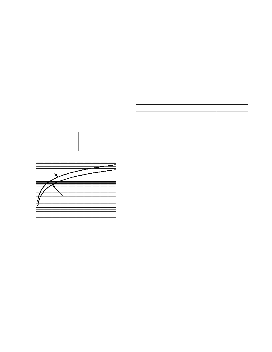
REV. B
≠20≠
AD7853/AD7853L
POWER VS. THROUGHPUT RATE
The main advantage of a full power-down after a conversion is
that it significantly reduces the power consumption of the part
at lower throughput rates. When using this mode of operation,
the AD7853 is only powered up for the duration of the conver-
sion. If the power-up time of the AD7853 is taken to be 5
µ
s
and it is assumed that the current during power-up is 4 mA typ,
then power consumption as a function of throughput can easily
be calculated. The AD7853 has a conversion time of 4.6
µ
s
with a 4 MHz external clock. This means the AD7853 con-
sumes 4 mA typ, (or 12 mW typ V
DD
= 3 V) for 9.6
µ
s in every
conversion cycle if the device is powered down at the end of a
conversion. If the throughput rate is 1 kSPS, the cycle time is
1000
µ
s and the average power dissipated during each cycle is
(9.6/1000)
◊
(12 mW) = 115
µ
W. The graph, Figure 24, shows
the power consumption of the AD7853 as a function of through-
put. Table VII lists the power consumption for various through-
put rates.
Table VII. Power Consumption vs. Throughput
Throughput Rate
Power
1 kSPS
115
µ
W
10 kSPS
1.15 mW
POWER ≠ mW
0.01
1
10
THROUGHPUT ≠ kSPS
0
10
20
30
40
50
0.1
5
15
25
35
45
AD7853 (4MHz CLK)
AD7853L (1.8MHz CLK)
Figure 26. Power vs. Throughput Rate
CALIBRATION SECTION
Calibration Overview
The automatic calibration that is performed on power-up en-
sures that the calibration options covered in this section will not
be required in a significant amount of applications. The user
will not have to initiate a calibration unless the operating condi-
tions change (CLKIN frequency, analog input mode, reference
voltage, temperature, and supply voltages). The AD7853/
AD7853L have a number of calibration features that may be
required in some applications and there are a number of advan-
tages in performing these different types of calibration. First, the
internal errors in the ADC can be reduced significantly to give
superior dc performance; and second, system offset and gain
errors can be removed. This allows the user to remove reference
errors (whether it be internal or external reference) and to make
use of the full dynamic range of the AD7853/AD7853L by ad-
justing the analog input range of the part for a specific system.
There are two main calibration modes on the AD7853/AD7853L,
self-calibration and system calibration. There are various op-
tions in both self-calibration and system calibration as outlined
previously in Table III. All the calibration functions can be
initiated by pulsing the
CAL pin or by writing to the control
register and setting the STCAL bit to 1. The timing diagrams
that follow involve using the
CAL pin.
The duration of each of the different types of calibrations is
given in Table VIII for the AD7853 with a 4 MHz master clock.
These calibration times are master clock dependent. Therefore
the calibration times for the AD7853L (CLKIN = 1.8 MHz)
will be larger than those quoted in Table VIII.
Table VIII. Calibration Times (AD7853 with 4 MHz CLKIN)
Type of Self- or System Calibration
Time
Full
31.25 ms
Gain + Offset
6.94 ms
Offset
3.47 ms
Gain
3.47 ms
Automatic Calibration on Power-On
The
CAL pin has a 0.15
µ
A pull-up current source connected to
it internally to allow for an automatic full self-calibration on
power-on. A full self-calibration will be initiated on power-on if
a capacitor is connected from the
CAL pin to DGND. The
internal current source connected to the
CAL pin charges up
the external capacitor and the time required to charge the exter-
nal capacitor will depend on the size of the capacitor itself. This
time should be large enough to ensure that the internal refer-
ence is settled before the calibration is performed. A 33 nF
capacitor is sufficient to ensure that the internal reference has
settled (see Power-Up Times) before a calibration is initiated
taking into account trigger level and current source variations on
the
CAL pin. However, if an external reference is being used,
this reference must have stabilized before the automatic calibra-
tion is initiated (a larger capacitor on the
CAL pin should be
used if the external reference has not settled when the autocali-
bration is initiated). Once the capacitor on the
CAL pin has
charged, the calibration will be performed which will take 32 ms
(4 MHz CLKIN). Therefore the autocalibration should be
complete before operating the part. After calibration, the part is
accurate to the 12-bit level and the specifications quoted on the
data sheet apply. There will be no need to perform another
calibration unless the operating conditions change or unless a
system calibration is required.
Self-Calibration Description
There are a four different calibration options within the self-
calibration mode. There is a full self-calibration where the DAC,
internal offset, and internal gain errors are calibrated out. Then,
there is the (Gain + Offset) self-calibration which calibrates out
the internal gain error and then the internal offset errors. The
internal DAC is not calibrated here. Finally, there are the self-
offset and self-gain calibrations which calibrate out the internal
offset errors and the internal gain errors respectively.
The internal capacitor DAC is calibrated by trimming each of
the capacitors in the DAC. It is the ratio of these capacitors to
each other that is critical, and so the calibration algorithm en-
sures that this ratio is at a specific value by the end of the cali-
bration routine. For the offset and gain there are two separate
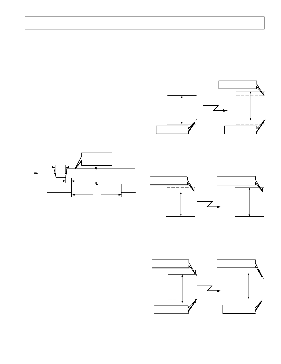
REV. B
≠21≠
AD7853/AD7853L
capacitors, one of which is trimmed when an offset or gain cali-
bration is performed. Again it is the ratio of these capacitors to
the capacitors in the DAC that is critical and the calibration
algorithm ensures that this ratio is at a specified value for both
the offset and gain calibrations.
In Bipolar Mode the midscale error is adjusted for an offset
calibration and the positive full-scale error is adjusted for the
gain calibration; in Unipolar Mode the zero-scale error is ad-
justed for an offset calibration and the positive full-scale error is
adjusted for a gain calibration.
Self-Calibration Timing
The diagram of Figure 27 shows the timing for a full self-
calibration. Here the BUSY line stays high for the full length of
the self-calibration. A self-calibration is initiated by bringing the
CAL pin low (which initiates an internal reset) and then high
again or by writing to the control register and setting the STCAL
bit to 1 (note that if the part is in a power-down mode, the
CAL
pulsewidth must take account of the power-up time). The BUSY line
is triggered high from the rising edge of
CAL (or the end of the
write to the control register if calibration is initiated in soft-
ware), and BUSY will go low when the full self-calibration is
complete after a time t
CAL
as shown in Figure 27.
t
1
= 100ns MIN,
t
15
= 2.5
t
CLKIN
MAX,
t
CAL
= 125013
t
CLKIN
(I/P)
BUSY (O/P)
t
1
t
15
t
CAL
Figure 27. Timing Diagram for Full Self-Calibration
For the self-(gain + offset), self-offset and self-gain calibrations,
the BUSY line will be triggered high by the rising edge of the
CAL signal (or the end of the write to the control register if
calibration is initiated in software) and will stay high for the full
duration of the self-calibration. The length of time that the
BUSY is high for will depend on the type of self-calibration that
is initiated. Typical figures are given in Table IX. The timing
diagrams for the other self-calibration options will be similar to
that outlined in Figure 27.
System Calibration Description
System calibration allows the user to take out system errors
external to the AD7853/AD7853L as well as calibrate the errors
of the AD7853/AD7853L itself. The maximum calibration
range for the system offset errors is
±
5% of V
REF
and for the
system gain errors is
±
2.5% of V
REF
. This means that the maxi-
mum allowable system offset voltage applied between the
AIN(+) and AIN(≠) pins for the calibration to adjust out this
error is
±
0.05
◊
V
REF
(i.e., the AIN(+) can be 0.05
◊
V
REF
above
AIN(≠) or 0.05
◊
V
REF
below AIN(≠)). For the system gain error
the maximum allowable system full-scale voltage, in unipolar
mode, that can be applied between AIN(+) and AIN(≠) for the
calibration to adjust out this error is V
REF
±
0.025
◊
V
REF
(i.e.,
the AIN(+) can be V
REF
+ 0.025
◊
V
REF
above AIN(≠) or V
REF
≠
0.025
◊
V
REF
above AIN(≠)). If the system offset or system gain
errors are outside the ranges mentioned, the system calibration
algorithm will reduce the errors as much as the trim range allows.
Figures 33 through 35 illustrate why a specific type of system
calibration might be used. Figure 33 shows a system offset cali-
bration (assuming a positive offset) where the analog input
range has been shifted upwards by the system offset after the
system offset calibration is completed. A negative offset may
also be accounted for by a system offset calibration.
MAX SYSTEM FULL SCALE
IS 2.5% FROM V
REF
ANALOG
INPUT
RANGE
V
REF
≠ 1LSB
SYS OFFSET
AGND
V
REF
+ SYS OFFSET
MAX SYSTEM OFFSET
IS 5% OF V
REF
ANALOG
INPUT
RANGE
V
REF
≠ 1LSB
SYS OFFSET
AGND
SYSTEM OFFSET
CALIBRATION
MAX SYSTEM OFFSET
IS 5% OF V
REF
Figure 28. System Offset Calibration
Figure 29 shows a system gain calibration (assuming a system
full scale greater than the reference voltage) where the analog
input range has been increased after the system gain calibration
is completed. A system full-scale voltage less than the reference
voltage may also be accounted for a by a system gain calibration.
MAX SYSTEM FULL SCALE
IS 2.5% FROM V
REF
ANALOG
INPUT
RANGE
V
REF
≠ 1LSB
AGND
SYS FULL S.
ANALOG
INPUT
RANGE
V
REF
≠ 1LSB
SYS FULL S.
AGND
SYSTEM GAIN
CALIBRATION
MAX SYSTEM FULL SCALE
IS 2.5% FROM V
REF
Figure 29. System Gain Calibration
Finally in Figure 30 both the system offset and gain are ac-
counted for by the system offset followed by a system gain cali-
bration. First the analog input range is shifted upwards by the
positive system offset and then the analog input range is ad-
justed at the top end to account for the system full scale.
ANALOG
INPUT
RANGE
SYS F.S.
SYS OFFSET
V
REF
+ SYS OFFSET
ANALOG
INPUT
RANGE
V
REF
≠ 1LSB
SYS F. S.
AGND
SYSTEM OFFSET
CALIBRATION
FOLLOWED BY
SYSTEM GAIN
CALIBRATION
MAX SYSTEM FULL SCALE
IS 2.5% FROM V
REF
SYS OFFSET
MAX SYSTEM OFFSET
IS 5% OF V
REF
MAX SYSTEM OFFSET
IS 5% OF V
REF
AGND
V
REF
≠ 1LSB
MAX SYSTEM FULL SCALE
IS 2.5% FROM V
REF
Figure 30. System (Gain + Offset) Calibration
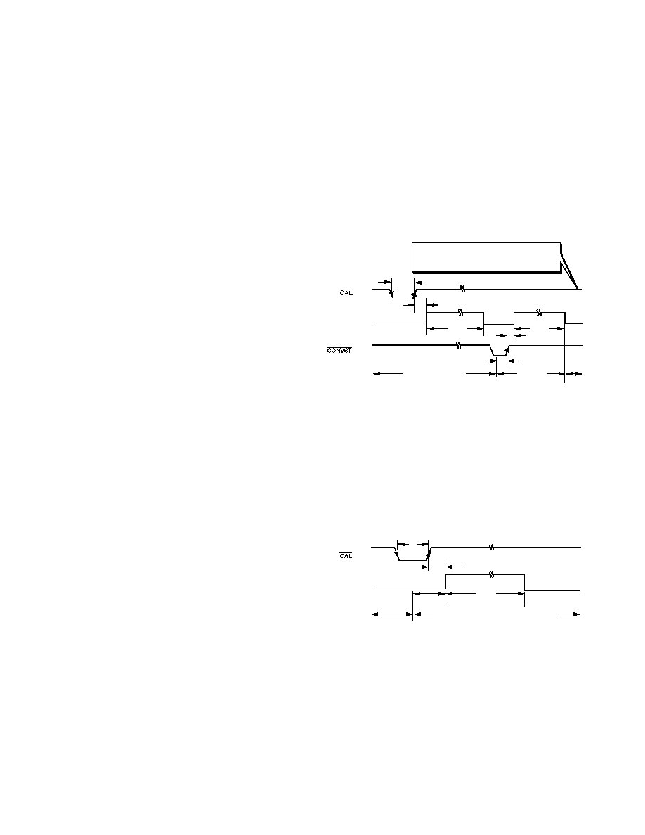
REV. B
≠22≠
AD7853/AD7853L
System Gain and Offset Interaction
The inherent architecture of the AD7853/AD7853L leads to an
interaction between the system offset and gain errors when a
system calibration is performed. Therefore it is recommended to
perform the cycle of a system offset calibration followed by a
system gain calibration twice. Separate system offset and system
gain calibrations reduce the offset and gain errors to at least the
12-bit level. By performing a system offset calibration first and a
system gain calibration second, priority is given to reducing the
gain error to zero before reducing the offset error to zero. If the
system errors are small, a system offset calibration would be
performed, followed by a system gain calibration. If the systems
errors are large (close to the specified limits of the calibration
range), this cycle would be repeated twice to ensure that the
offset and gain errors were reduced to at least the 12-bit level.
The advantage of doing separate system offset and system gain
calibrations is that the user has more control over when the
analog inputs need to be at the required levels, and the
CONVST
signal does not have to be used.
Alternatively, a system (gain + offset) calibration can be per-
formed. It is recommended to perform three system (gain +
offset) calibrations to reduce the offset and gain errors to the
12-bit level. For the system (gain + offset) calibration priority is
given to reducing the offset error to zero before reducing the
gain error to zero. Thus if the system errors are small then two
system (gain + offset) calibrations will be sufficient. If the sys-
tem errors are large (close to the specified limits of the calibra-
tion range), three system (gain + offset) calibrations may be
required to reduced the offset and gain errors to at least the
12-bit level. There will never be any need to perform more than
three system (offset + gain) calibrations.
In Bipolar Mode the midscale error is adjusted for an offset
calibration and the positive full-scale error is adjusted for the
gain calibration; in Unipolar Mode the zero-scale error is ad-
justed for an offset calibration and the positive full-scale error is
adjusted for a gain calibration.
System Calibration Timing
The calibration timing diagram in Figure 31 is for a full system
calibration where the falling edge of
CAL initiates an internal
reset before starting a calibration (note that if the part is in power-
down mode the
CAL pulsewidth must take account of the power-up
time). If a full system calibration is to be performed in software,
it is easier to perform separate gain and offset calibrations so
that the CONVST bit in the control register does not have to be
programmed in the middle of the system calibration sequence.
The rising edge of
CAL starts calibration of the internal DAC
and causes the BUSY line to go high. If the control register is
set for a full system calibration, the
CONVST must be used
also. The full-scale system voltage should be applied to the
analog input pins from the start of calibration. The BUSY line
will go low once the DAC and system gain calibration are
complete. Next the system offset voltage is applied to the AIN
pin for a minimum setup time (t
SETUP
) of 100 ns before the
rising edge of the
CONVST and remain until the BUSY signal
goes low. The rising edge of the
CONVST starts the system
offset calibration section of the full system calibration and also
causes the BUSY signal to go high. The BUSY signal will go
low after a time t
CAL2
when the calibration sequence is complete.
The timing for a system (gain + offset) calibration is very similar
to that of Figure 31, the only difference being that the time
t
CAL1
will be replaced by a shorter time of the order of t
CAL2
as
the internal DAC will not be calibrated. The BUSY signal will
signify when the gain calibration is finished and when the part is
ready for the offset calibration.
t
1
= 100ns MIN,
t
14
= 50/90ns MIN 5V/3V,
t
15
= 2.5
t
CLKIN
MAX,
t
CAL1
= 111114
t
CLKIN
MAX,
t
CAL2
= 13899
t
CLKIN
(I/P)
BUSY (O/P)
(I/P)
t
1
AIN (I/P)
t
15
t
CAL1
t
CAL2
t
16
t
SETUP
V
SYSTEM FULL SCALE
V
OFFSET
Figure 31. Timing Diagram for Full System Calibration
The timing diagram for a system offset or system gain calibra-
tion is shown in Figure 32. Here again the
CAL is pulsed and
the rising edge of the
CAL initiates the calibration sequence (or
the calibration can be initiated in software by writing to the
control register). The rising edge of the
CAL causes the BUSY
line to go high and it will stay high until the calibration sequence is
finished. The analog input should be set at the correct level for a
minimum setup time (t
SETUP
) of 100 ns before the rising edge of
CAL and stay at the correct level until the BUSY signal goes
low.
(I/P)
BUSY (O/P)
AIN (I/P)
t
15
t
SETUP
t
1
t
CAL2
V
SYSTEM FULL SCALE
OR V
SYSTEM OFFSET
Figure 32. Timing Diagram for System Gain or System
Offset Calibration
REV. B
≠23≠
AD7853/AD7853L
SERIAL INTERFACE SUMMARY
Table IX details the five interface modes and the serial clock
edges from which the data is clocked out by the AD7853/
AD7853L (DOUT Edge) and that the data is latched in on
(DIN Edge). The logic level of the POLARITY pin is shown
and it is clear that this reverses the edges.
In Interface Modes 4 and 5 the
SYNC always clocks out the
first data bit and SCLK will clock out the subsequent bits.
In Interface Modes 1, 2, and 3 the
SYNC is gated with the
SCLK and the POLARITY pin. Thus the
SYNC may clock out
the MSB of data. Subsequent bits will be clocked out by the
serial clock, SCLK. The conditions for the
SYNC clocking out
the MSB of data is as follows:
With the POLARITY pin high the falling edge of
SYNC will clock
out the MSB if the serial clock is low when the
SYNC goes low.
With the POLARITY pin low the falling edge of
SYNC will clock
out the MSB if the serial clock is high when the
SYNC goes low.
Table IX. SCLK Active Edge for Different Interface Modes
Interface
POLARITY
DOUT
DIN
Mode
Pin
Edge
Edge
1, 2, 3
0
SCLK
SCLK
1
SCLK
SCLK
4, 5
0
SCLK
SCLK
1
SCLK
SCLK
Resetting the Serial Interface
When writing to the part via the DIN line there is the possibility
of writing data into the incorrect registers, such as the test regis-
ter for instance, or writing the incorrect data and corrupting the
serial interface. The
SYNC pin acts as a reset. Bringing the
SYNC pin high resets the internal shift register. The first data
bit after the next
SYNC falling edge will now be the first bit of a
new 16-bit transfer. It is also possible that the test register con-
tents were altered when the interface was lost. Therefore, once
the serial interface is reset, it may be necessary to write the 16-
bit word 0100 0000 0000 0010 to restore the test register to its
default value. Now the part and serial interface are completely
reset. It is always useful to retain the ability to program the
SYNC line from a port of the
µ
Controller/DSP to have the
ability to reset the serial interface.
Table X summarizes the interface modes provided by the
AD7853/AD7853L. It also outlines the various
µ
P/
µ
C to which
the particular interface is suited.
The interface mode is determined by the serial mode selection
pins SM1 and SM2. Interface Mode 2 is the default mode. Note
that Interface Mode 1 and 2 have the same combination of SM1
and SM2. Interface Mode 1 may only be set by programming
the control register (see section on control register). External
SCLK and
SYNC signals (SYNC may be hardwired low) are
required for Interfaces Modes 1, 2, and 3. In Interface Modes 4
and 5, the AD7853/AD7853L generates the SCLK and
SYNC.
Some of the more popular
µ
Processors,
µ
Controllers, and the
DSP machines that the AD7853/AD7853L will interface to
directly are mentioned here. This does not cover all
µ
Cs,
µ
Ps
and DSPs. The interface mode of the AD7853/AD7853L that is
mentioned here for a specific
µ
C,
µ
P, or DSP is only a guide
and in most cases another interface mode may work just as well.
A more detailed timing description on each of the interface
modes follows.
Table X. Interface Mode Description
SM1
SM2
Processor/
Interface
Pin
Pin
Controller
Mode
0
0
8XC51
1 (2-Wire)
8XL51
(DIN is an Input/
PIC17C42
Output pin)
0
0
68HC11
2 (3-Wire, SPI/QSPI)
68L11
(Default Mode)
0
1
68HC16
3 (QSPI)
PIC16C64
(External Serial
ADSP-21xx
Clock, SCLK, and
DSP56000
External Frame Sync,
DSP56001
SYNC, are required)
DSP56002
DSP56L002
TMS320C30
1
0
68HC16
4 (DSP is Slave)
(AD7853/AD7853L
generates a
noncontinuous
[16 clocks] Serial
Clock, SCLK, and the
Frame Sync,
SYNC)
1
1
ADSP-21xx
5 (DSP is Slave)
DSP56000
(AD7853/AD7853L
DSP56001
generates a
DSP56002
continuous Serial
DSP56L002
Clock, SCLK, and the
TMS320C20
Frame Sync,
SYNC)
TMS320C25
TMS320C30
TMS320C5x
TMS320LC5x
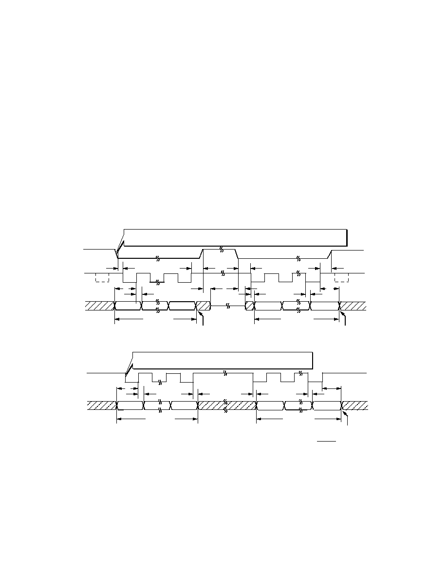
REV. B
≠24≠
AD7853/AD7853L
DETAILED TIMING SECTION
Mode 1 (2-Wire 8051 Interface)
The read and writing takes place on the DIN line and the con-
version is initiated by pulsing the
CONVST pin (note that in
every write cycle the 2/
3 Mode bit must be set to 1). The con-
version may be started by setting the
CONVST bit in the con-
trol register to 1 instead of using the
CONVST line.
Below in Figure 33 and in Figure 34 are the timing diagrams for
Interface Mode 1 in Table X where we are in the 2-wire inter-
face mode. Here the DIN pin is used for both input and output
as shown. The
SYNC input is level triggered active low and can
be pulsed (Figure 33) or can be constantly low (Figure 34).
In Figure 33 the part samples the input data on the rising edge
of SCLK. After the 16th rising edge of SCLK the DIN is con-
figured as an output. When the
SYNC is taken high the DIN is
three-stated. Taking
SYNC low disables the three-state on the
DIN pin and the first SCLK falling edge clocks out the first data
bit. Once the 16 clocks have been provided the DIN pin will
automatically revert back to an input after a time t
14
. Note that a
continuous SCLK shown by the dotted waveform in Figure 33
can be used provided that the
SYNC is low for only 16 clock
pulses in each of the read and write cycles. The POLARITY pin
may be used to change the SCLK edge which the data is sampled
on and clocked out on.
In Figure 34 the
SYNC line is tied low permanently and this
results in a different timing arrangement. With
SYNC tied low
permanently the DIN pin will never be three-stated. The 16th
rising edge of SCLK configures the DIN pin as an input or an
output as shown in the diagram. Here no more than 16 SCLK
pulses must occur for each of the read and write operations.
If reading from and writing to the calibration registers in this
interface mode, all the selected calibration registers must be
read from or written to. The read and write operations cannot
be aborted. When reading from the calibration registers, the
DIN pin will remain as an output for the full duration of all the
calibration register read operations. When writing to the calibra-
tion registers, the DIN pin will remain as an input for the full
duration of all the calibration register write operations.
SCLK (I/P)
SYNC
(I/P)
t
3
t
8
DIN (I/O)
DB15
DB0
DB0
t
3
t
11
t
6
POLARITY PIN
LOGIC HIGH
1
16
16
1
t
5A
t
12
DIN BECOMES AN INPUT
DB15
THREE-STATE
DATA READ
DATA WRITE
t
7
t
6
t
14
t
11
DIN BECOMES AN OUTPUT
t
3
= ≠0.4 t
SCLK
MIN (NONCONTINUOUS SCLK) ≠/+0.4 t
SCLK
MIN/MAX (CONTINUOUS SCLK),
t
6
= 75/115 MAX (5V/3V), t
7
= 40/60ns
MIN (5V/3V), t
8
= 20/30
MIN (5V/3V)
Figure 33. Timing Diagram for Read/Write Operation with DIN as an Input/Output (i.e., Interface Mode 1, SM1 = SM2 = 0)
SCLK (I/P)
t
8
DIN (I/O)
DB15
DB0
DB0
t
6
1
16
16
1
DIN BECOMES AN INPUT
DB15
DATA READ
DATA WRITE
t
7
t
6
t
14
t
6
= 75/115 MAX (5V/3V), t
7
= 40/60ns
MIN (5V/3V), t
8
= 20/30
MIN (5V/3V),
t
13
= 90/130 MAX (5V/3V), t
14
= 50/90ns
MAX (5V/3V)
6
t
13
POLARITY PIN
LOGIC HIGH
Figure 34. Timing Diagram for Read/Write Operation with DIN as an Input/Output and SYNC Input Tied Low
(i.e., Interface Mode 1, SM1 = SM2 = 0)
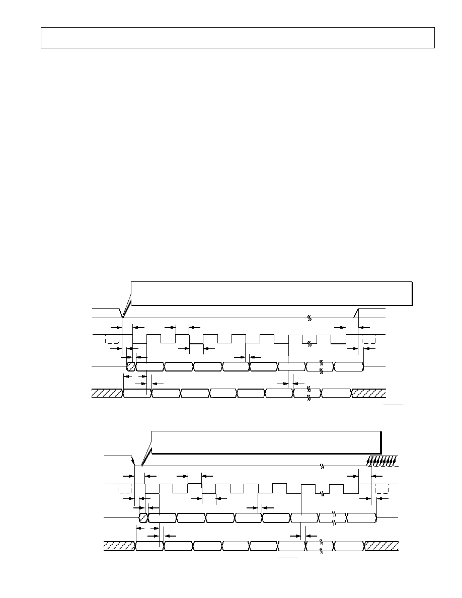
REV. B
≠25≠
AD7853/AD7853L
high after the 16th SCLK rising edge as shown by the dotted
SYNC line in Figure 36. Thus a frame sync that gives a high
pulse, of one SCLK cycle minimum duration, at the beginning
of the read/write operation may be used. The rising edge of
SYNC enables the three-state on the DOUT pin. The falling
edge of
SYNC disables the three-state on the DOUT pin, and
data is clocked out on the falling edge of SCLK. Once
SYNC
goes high, the three-state on the DOUT pin is enabled. The
data input is sampled on the rising edge of SCLK and thus has
to be valid a time, t
7
, before this rising edge. The POLARITY
pin may be used to change the SCLK edge which the data is
sampled on and clocked out on. If resetting the interface is
required, the
SYNC must be taken high and then low.
Modes 4 and 5 (Self-Clocking Modes)
The timing diagrams in Figure 38 and Figure 39 are for Inter-
face Modes 4 and 5. Interface Mode 4 has a noncontinuous
SCLK output and Interface Mode 5 has a continuous SCLK
output. These modes of operation are especially different to all
the other modes since the SCLK and
SYNC are outputs. The
SYNC is generated by the part as is the SCLK. The master
clock at the CLKIN pin is routed directly to the SCLK pin for
Interface Mode 5 (Continuous SCLK) and the CLKIN signal is
gated with the
SYNC to give the SCLK (noncontinuous) for
Interface Mode 4.
Mode 2 (3-Wire SPI/QSPI Interface Mode)
This is the DEFAULT INTERFACE MODE.
In Figure 35 below we have the timing diagram for Interface
Mode 2 which is the SPI/QSPI interface mode. Here the
SYNC
input is active low and may be pulsed or tied permanently low.
If
SYNC is permanently low 16 clock pulses must be applied to
the SCLK pin for the part to operate correctly, and with a
pulsed
SYNC input a continuous SCLK may be applied provided
SYNC is low for only 16 SCLK cycles. In Figure 30 the SYNC
going low disables the three-state on the DOUT pin. The first
falling edge of the SCLK after the
SYNC going low clocks out
the first leading zero on the DOUT pin. The DOUT pin is
three-stated again a time t
12
after the
SYNC goes high. With the
DIN pin the data input has to be set up a time, t
7
, before the
SCLK rising edge as the part samples the input data on the
SCLK rising edge in this case. The POLARITY pin may be
used to change the SCLK edge which the data is sampled on
and clocked out on. If resetting the interface is required, the
SYNC must be taken high and then low.
Mode 3 (QSPI Interface Mode)
Figure 36 shows the timing diagram for Interface Mode 3. In
this mode the DSP is the master and the part is the slave. Here
the
SYNC input is edge triggered from high to low, and the 16
clock pulses are counted from this edge. Since the clock pulses
are counted internally then the
SYNC signal does not have to go
t
3
= ≠0.4 t
CLKIN
MIN (NONCONTINUOUS SCLK) ≠/+0.4 t
SCLK
MIN/MAX (CONTINUOUS SCLK),
t
6
= 75/115 MAX (5V/3V), t
7
= 40/60ns
MIN (5V/3V), t
8
= 20/30
MIN (5V/3V),
t
11
= 20/30 MIN (NONCONTINUOUS SCLK) (5V/3V), (30/50)/0.4 t
SCLK
= ns
MIN/MAX (CONTINUOUS SCLK) (5V/3V)
DOUT (O/P)
SCLK (I/P)
SYNC
(I/P)
DB0
t
3
t
8
t
10
t
9
t
5
DIN (I/P)
THREE-
STATE
THREE-
STATE
t
11
t
6
t
6
t
8
1
6
2
3
4
5
16
POLARITY PIN
LOGIC HIGH
t
12
DB11
DB10
DB15
DB14
DB13
DB12
DB0
DB11
DB10
DB15
DB14
DB13
DB12
t
7
Figure 35. SPI/QSPI Mode 2 Timing Diagram for Read/Write Operation with DIN Input, DOUT Output and SYNC Input
(SM1 = SM2 = 0)
t
7
DOUT (O/P)
SCLK (I/P)
SYNC
(I/P)
DB0
t
3
t
8
t
10
t
9
t
5
DIN (I/P)
THREE-
STATE
THREE-
STATE
t
11
t
6
t
6
t
8
1
6
2
3
4
5
16
POLAR PIN
LOGIC HIGHITY
t
12
DB11
DB10
DB15
DB14
DB13
DB12
DB0
DB11
DB10
DB15
DB14
DB13
DB12
t
3
= ≠0.4 t
CLKIN
MIN (NONCONTINUOUS SCLK) ≠/+0.4 t
SCLK
MIN/MAX (CONTINUOUS SCLK),
t
6
= 75/115 MAX (5V/3V), t
7
= 40/60ns
MIN (5V/3V), t
8
= 20/30
MIN (5V/3V),
t
11
= 20/30 MIN (5V/3V)
Figure 36. QSPI Mode 3 Timing Diagram for Read/Write Operation with SYNC Input Edge Triggered (SM1 = 0, SM2 = 1)
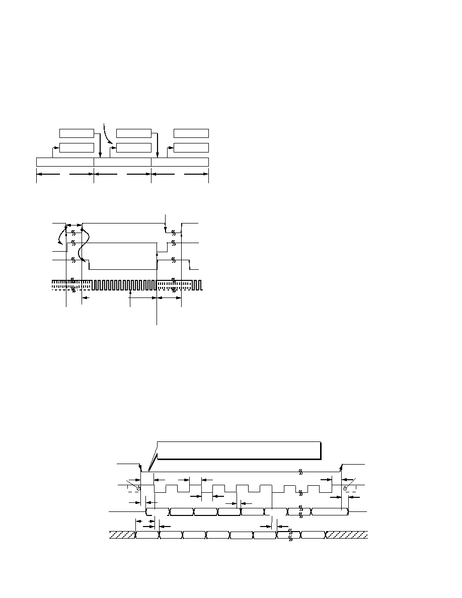
REV. B
≠26≠
AD7853/AD7853L
The most important point about these two modes of operation
mode is that the result of the current conversion is clocked
out during the same conversion and a write to the part dur-
ing this conversion is for the next conversion. The arrangement
is shown in Figure 37. Figure 38 and Figure 39 show more
detailed timing for the arrangement of Figure 37.
WRITE N+1
CONVERSION N
READ N
5 s
WRITE N+2
CONVERSION N+1
READ N+1
WRITE N+3
CONVERSION N+2
READ N+2
5 s
THE CONVERSION RESULT DUE TO
WRITE N+1 IS READ HERE
5 s
Figure 37.
t
1
CONVST
(I/P)
SCLK
(O/P)
CONVERSION ENDS
4.6 s LATER
SERIAL READ
AND WRITE
OPERATIONS
OUTPUT SERIAL SHIFT
REGISTER IS RESET
READ OPERATION
SHOULD END 500ns
PRIOR TO NEXT RISING
400ns MIN
BUSY
(O/P)
SYNC
(O/P)
CONVERSION IS INITIATED
AND TRACK/HOLD GOES
INTO HOLD
EDGE OF
CONVST
t
1
= 100ns MIN
t
CONVERT
= 4.6 s
Figure 38. Mode 4, 5 Timing Diagram (SM1 = 1, SM2 = 1
and 0)
In Figure 38 the first point to note is that the BUSY,
SYNC,
and SCLK are all outputs from the AD7853/AD7853L with the
CONVST being the only input signal. Conversion is initiated
with the
CONVST signal going low. This CONVST falling
edge also triggers the BUSY to go high. The
CONVST signal
rising edge triggers the
SYNC to go low after a short delay
(0.5 t
CLKIN
to 1.5 t
CLKIN
typically) after which the SCLK will
clock out the data on the DOUT pin during conversion. The
data on the DIN pin is also clocked in to the AD7853/AD7853L
by the same SCLK for the next conversion. The read/write
operations must be complete after sixteen clock cycles (which
takes 4.6
µ
s approximately from the rising edge of
CONVST assum-
ing a 4 MHz CLKIN). At this time the conversion will be com-
plete, the
SYNC will go high, and the BUSY will go low. The
next falling edge of the
CONVST must occur at least 400 ns
after the falling edge of BUSY to allow the track/hold amplifier
adequate acquisition time as shown in Figure 38. This gives a
throughput time of 5
µ
s. The maximum throughput rate in this
case is 200 kHz (AD7853) and 100 kHz (AD7853L).
In these interface modes the part is now the master and the DSP
is the slave. Figure 39 is an expansion of Figure 38. The
AD7853/AD7853L will ensure
SYNC goes low after the rising
edge C of the continuous SCLK (Interface Mode 5) in Figure
39. Only in the case of a noncontinuous SCLK (Interface Mode
4) will the time t
4
apply. The first data bit is clocked out from
the falling edge of
SYNC. The SCLK rising edge clocks out all
subsequent bits on the DOUT pin. The input data present on
the DIN pin is clocked in on the rising edge of the SCLK. The
POLARITY pin may be used to change the SCLK edge which
the data is sampled on and clocked out on. The
SYNC will go
high after the 16th SCLK rising edge and before the falling edge
D of the continuous SCLK in Figure 39. This ensures the part
will not clock in an extra bit from the DIN pin or clock out an
extra bit on the DOUT pin.
If the user has control of the
CONVST pin but does not want to
exercise it for every conversion, the control register may be used
to start a conversion. Setting the CONVST bit in the control
register to 1 starts a conversion. If the user does not have con-
trol of the
CONVST pin, a conversion should not be initiated
by writing to the control register. The reason for this is that the
user may get "locked out" and not be able to perform any fur-
ther write/read operations. When a conversion is started by
writing to the control register, the
SYNC goes low and read/
write operations take place while the conversion is in progress.
However, once the conversion is complete, there is no way of
writing to the part unless the
CONVST pin is exercised. The
CONVST signal triggers the SYNC signal low which allows
read/write operations to take place.
SYNC must be low to per-
form read/write operations. The
SYNC is triggered low by the
CONVST signal rising edge or setting the CONVST bit in the
control register to 1. Therefore if there is not full control of the
CONVST pin the user may end up getting "locked out."
DOUT (O/P)
SCLK (O/P)
SYNC
(O/P)
DIN (I/P)
t
8
POLARITY PIN
LOGIC HIGH
1
2
3
4
5
6
16
DB0
DB15
DB14
DB13
DB12
DB11
DB10
DB0
THREE-
STATE
THREE-
STATE
DB11
DB10
DB14
DB13
DB12
t
6
t
10
t
9
t
12
t
11A
t
4
t
5
DB15
t
8
t
7
C
D
t
4
= 0.6t
SCLK
(NONCONTINUOUS SCLK), t
6
= 75/115 MAX (5V/3V),
t
7
= 40/60ns
MIN (5V/3V), t
8
= 20/30
MIN (5V/3V), t
11A
= 50ns MAX
Figure 39. Timing Diagram for Read/Write with
SYNC Output and SCLK Output (Continuous and Noncontinuous)
(i.e., Operating Mode Numbers 4 and 5, SM1 = 1, SM2 = 1 and 0)
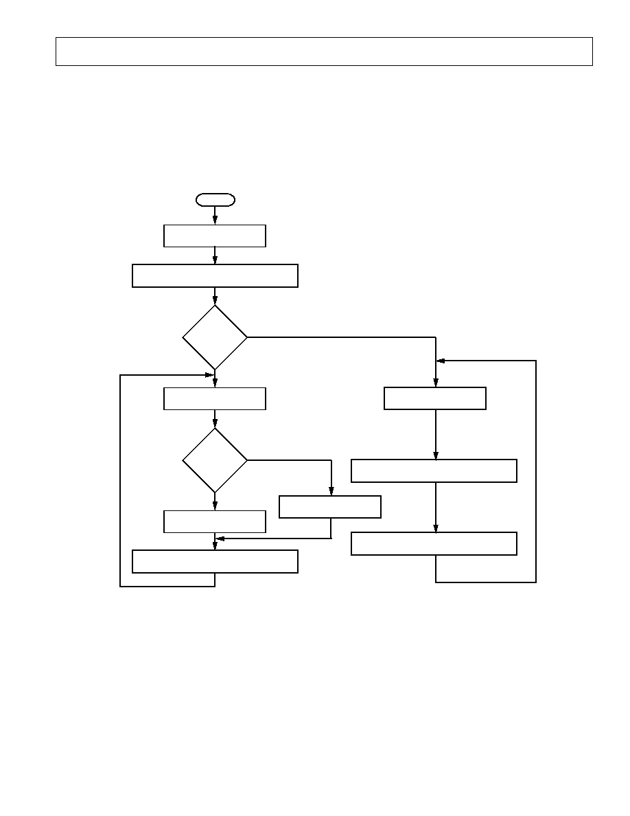
REV. B
≠27≠
AD7853/AD7853L
CONFIGURING THE AD7853/AD7853L
AD7853/AD7853L as a Read-Only ADC
The AD7853/AD7853L contains fourteen on-chip registers
which can be accessed via the serial interface. In the majority of
applications it will not be necessary to access all of these regis-
ters. Figure 38 outlines a flowchart of the sequence which is
used to configure the AD7853/AD7853L as a Read-Only ADC.
In this case there is no writing to the on-chip registers and only
the conversion result data is read from the part. Interface Mode
1 cannot be used in this case as it is necessary to write to the
control register to set Interface Mode 1. Here the CLKIN signal
is applied directly after power-on, the CLKIN signal must be
present to allow the part to perform a calibration. This auto-
matic calibration will be completed approximately 32 ms after
the AD7853 has powered up (4 MHz CLK).
SERIAL
INTERFACE
MODE
?
POWER-ON, APPLY CLKIN SIGNAL,
WAIT FOR AUTOMATIC CALIBRATION
DIN CONNECTED TO DGND
NO
YES
START
WAIT FOR BUSY SIGNAL
TO GO LOW
PULSE
CONVST
PIN
READ
DATA
DURING
CONVERSION
?
WAIT APPROXIMATLY 200ns
AFTER
CONVST
RISING EDGE
APPLY
SYNC
(IF REQUIRED), SCLK AND READ
CONVERSION RESULT ON DOUT PIN
PULSE
CONVST
PIN
SYNC
AUTOMATICALLY GOES LOW
AFTER
CONVST
RISING EDGE
SCLK AUTOMATICALLY ACTIVE, READ
CONVERSION RESULT ON DOUT PIN
4, 5
2, 3
Figure 40. Flowchart for Setting Up and Reading from the AD7853/AD7853L
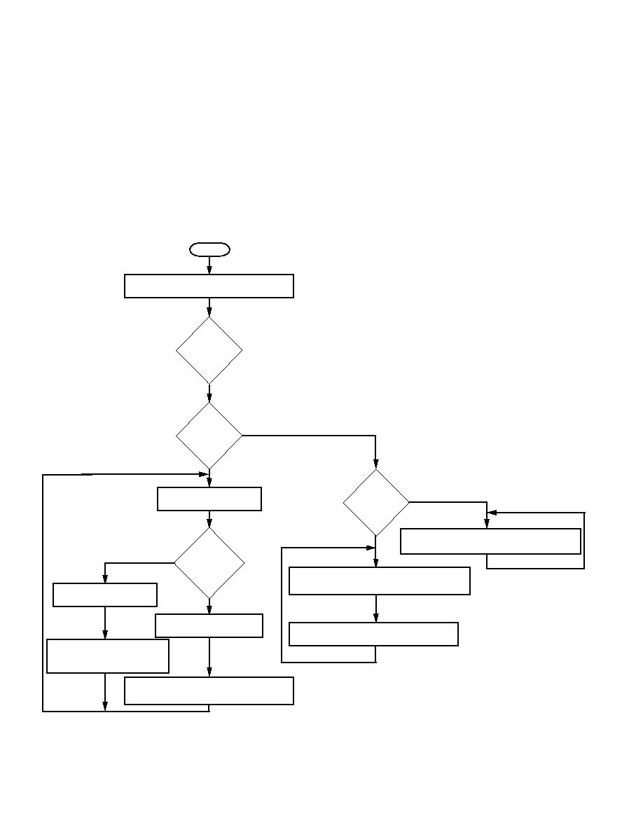
REV. B
≠28≠
AD7853/AD7853L
Writing to the AD7853/AD7853L
For accessing the on-chip registers it is necessary to write to the
part. To enable Serial Interface Mode 1, the user must also
write to the part. Figure 41 through 43 outline flowcharts of
how to configure the AD7853/AD7853L for each of the differ-
ent serial interface modes. The continuous loops on all diagrams
indicate the sequence for more than one conversion. The options
of using a hardware (pulsing the
CONVST pin) or software
(setting the CONVST bit to 1) conversion start, and reading/
writing during or after conversion are shown in Figures 41 and
42. If the
CONVST pin is never used then it should be tied to
DV
DD
permanently. Where reference is made to the BUSY bit
equal to a Logic 0, to indicate the end of conversion, the user in
this case would poll the BUSY bit in the status register.
Interface Modes 2 and 3 Configuration
Figure 41 shows the flowchart for configuring the part in Inter-
face Modes 2 and 3. For these interface modes, the read and
write operations take place simultaneously via the serial port.
Writing all 0s ensures that no valid data is written to any of the
registers. When using the software conversion start and transfer-
ring data during conversion, Note must be obeyed.
SERIAL
INTERFACE
MODE
?
POWER-ON, APPLY CLKIN SIGNAL,
WAIT FOR AUTOMATIC CALIBRATION
NO
YES
START
WAIT FOR BUSY SIGNAL TO GO
LOW OR WAIT FOR BUSY BIT = 0
PULSE
CONVST
PIN
TRANSFER
DATA
DURING
CONVERSION
?
APPLY
SYNC
(IF REQUIRED), SCLK, READ
CURRENT CONVERSION RESULT ON DOUT PIN,
AND WRITE ALL 0s ON DIN PIN
WAIT FOR BUSY SIGNAL TO GO LOW
OR WAIT FOR BUSY BIT = 0
APPLY
SYNC
(IF REQUIRED), SCLK, WRITE TO CONTROL
REGISTER SETTING CONVST BIT TO 1, READ CURRENT
CONVERSION RESULT ON DOUT PIN
2, 3
INITIATE
CONVERSION
IN
SOFTWARE
?
WAIT APPROXIMATLY 200ns
AFTER
CONVST
RISING EDGE
APPLY
SYNC
(IF REQUIRED),
SCLK, READ PREVIOUS CONVERSION
RESULT ON DOUT PIN,
AND WRITE ALL 0s ON DIN PIN
NO
YES
TRANSFER
DATA DURING
CONVERSION
APPLY
SYNC
(IF REQUIRED), SCLK, WRITE TO CONTROL
REGISTER SETTING CONVST BIT TO 1, READ PREVIOUS
CONVERSION RESULT ON DOUT PIN (SEE NOTE)
YES
NO
NOTE:
WHEN USING THE SOFTWARE CONVERSION START AND TRANSFERRING
DATA DURING CONVERSION THE USER MUST ENSURE THE CONTROL
REGISTER WRITE OPERATION EXTENDS BEYOND THE FALLING EDGE OF
BUSY. THE FALLING EDGE OF BUSY RESETS THE CONVST BIT TO 0 AND
ONLY AFTER THIS TIME CAN IT BE REPROGRAMMED TO 1 TO START THE
NEXT CONVERSION.
Figure 41. Flowchart for Setting Up, Reading and Writing in Interface Modes 2 and 3
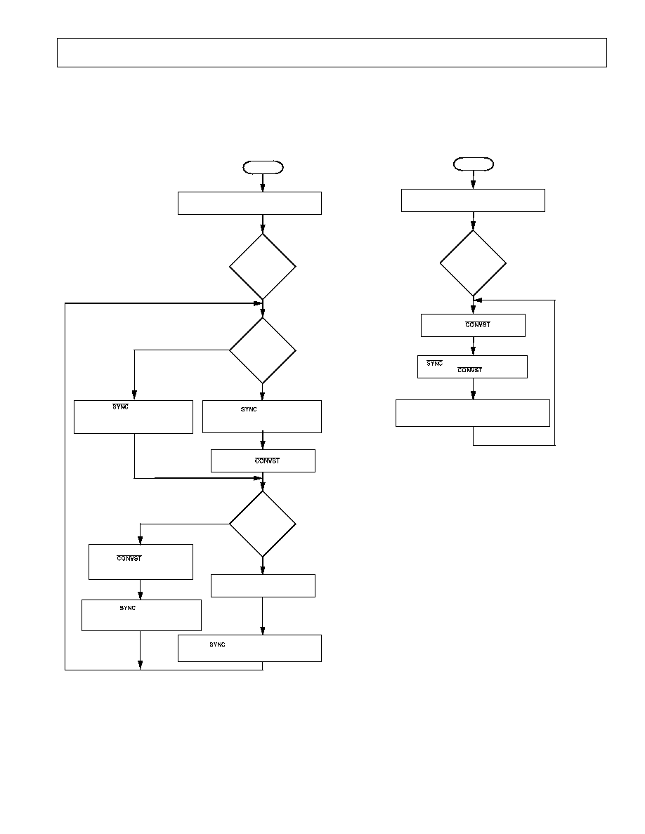
REV. B
≠29≠
AD7853/AD7853L
Interface Mode 1 Configuration
Figure 42 shows the flowchart for configuring the part in
Interface Mode 1. This mode of operation can only enabled by
writing to the control register and setting the 2/
3 MODE bit.
Reading and writing cannot take place simultaneously in this
mode as the DIN pin is used for both reading and writing.
APPLY
(IF REQUIRED),
SCLK, WRITE TO CONTROL REGISTER
SETTING THE TWO-WIRE MODE
SERIAL
INTERFACE
MODE
?
POWER-ON, APPLY CLKIN SIGNAL,
WAIT 150ms FOR AUTOMATIC CALIBRATION
NO
YES
START
WAIT FOR BUSY SIGNAL TO GO
LOW OR WAIT FOR BUSY BIT = 0
PULSE
PIN
READ
DATA
DURING
CONVERSION
?
APPLY
(IF REQUIRED), SCLK, READ
CURRENT CONVERSION RESULT ON DIN PIN
1
INITIATE
CONVERSION
IN
SOFTWARE
?
WAIT APPROXIMATLY 200ns
AFTER
RISING EDGE
OR AFTER END OF CONTROL
REGISTER WRITE
APPLY
(IF REQUIRED),
SCLK, READ PREVIOUS CONVERSION
RESULT ON DIN PIN
NO
YES
APPLY
(IF REQUIRED),
SCLK, WRITE TO CONTROL REGISTER
SETTING THE TWO-WIRE MODE
AND CONVST BIT TO 1
Figure 42. Flowchart for Setting Up, Reading and Writing
in Interface Mode 1
Interface Modes 4 and 5 Configuration
Figure 43 shows the flowchart for configuring the AD7853/
AD7853L in Interface Modes 4 and 5, the self-clocking modes.
In this case it is not recommended to use the software conver-
sion start option. The read and write operations always occur
simultaneously and during conversion.
SERIAL
INTERFACE
MODE
?
POWER-ON, APPLY CLKIN SIGNAL,
WAIT 150ms FOR AUTOMATIC CALIBRATION
START
AUTOMATICALLY GOES
LOW AFTER
RISING EDGE
PULSE
PIN
SCLK AUTOMATICALLY ACTIVE, READ CURRENT
CONVERSION RESULT ON DOUT PIN, WRITE
TO CONTROL REGISTER ON DIN PIN
4, 5
Figure 43. Flowchart for Setting Up, Reading and Writing
in Interface Modes 4 and 5
REV. B
≠30≠
AD7853/AD7853L
MICROPROCESSOR INTERFACING
In many applications, the user may not require the facility of
writing to the on-chip registers. The user may just want to
hardwire the relevant pins to the appropriate levels and read the
conversion result. In this case the DIN pin can be tied low so
that the on-chip registers are never used. Now the part will
operate as a nonprogrammable analog to digital converter where
the
CONVST is applied, a conversion is performed and the
result may be read using the SCLK to clock out the data from
the output register on to the DOUT pin. Note that the DIN pin
cannot be tied low when using the two-wire interface mode of
operation.
The SCLK can also be connected to the CLKIN pin if the user
does not want to have to provide separate serial and master
clocks in Interface Modes 1, 2, and 3. With this arrangement
the
SYNC signal must be low for 16 SCLK cycles in Interface
Modes 1 and 2 for the read and write operations. For Interface
Mode 3 the
SYNC can be low for more than 16 SCLK cycles
for the read and write operations. Note that in Interface Modes
4 and 5 the CLKIN and SCLK cannot be tied together as the
SCLK is an output and the CLKIN is an input.
DIN
DOUT
SYNC
CONVST
CLKIN
SCLK
AD7853/AD7853L
4 MHz/1.8MHz
MASTER
CLOCK
SYNC
SIGNAL
TO GATE
THE SCLK
SERIAL DATA
OUTPUT
CONVERSION
START
Figure 44. Simplified Interface Diagram with DIN
Grounded and SCLK Tied to CLKIN
AD7853/AD7853L to 8XC51/PIC17C42 Interface
Figure 45 shows the AD7853/AD7853L interface to the 8XC51/
PIC17C42. The 8XL51 is for interfacing to the AD7853/AD7853L
when the supply is at 3 V. The 8XC51/PIC17C42 only run at
5 V. The 8XC51 is in Mode 0 operation. This is a two-wire
interface consisting of the SCLK and the DIN which acts as a
bidirectional line. The
SYNC is tied low. The BUSY line can be
used to give an interrupt driven system but this would not nor-
mally be the case with the 8XC51/PIC17C42. For the 8XC51
12 MHz version, the serial clock will run at a maximum of
1 MHz so that the serial interface to the AD7853/AD7853L will
only be running at 1 MHz. The CLKIN signal must be provided
separately to the AD7853/AD7853L from a port line on the
8XC51 or from a source other than the 8XC51. Here the SCLK
cannot be tied to the CLKIN as the 8XC51 only provides a
noncontinuous serial clock. The
CONVST signal can be pro-
vided from an external timer or conversion can be started in
software if required. The sequence of events would typically be
writing to the control register via the DIN line setting a conver-
sion start and the 2-wire interface mode (this would be per-
formed in two 8-bit writes), wait for the conversion to be
finished (4.5
µ
s with 4 MHz CLKIN), read the conversion re-
sult data on the DIN line (this would be performed in two 8-bit
reads), and then repeat the sequence. The maximum serial
frequency will be determined by the data access and hold times
of the 8XC51/PIC16C42 and the AD7853/AD7853L.
(8XC51/L51)
/PIC17C42
P3.0/DT
P3.1/CK
AD7853/AD7853L
CONVST
CLKIN
SCLK
DIN
SYNC
SM1
SM2
POLARITY
OPTIONAL
4MHz/1.8MHz
BUSY
(
INT0
/P3.2)/INT
DV
DD
FOR 8XC51/L51
DGND FOR PIC17C42
MASTER
SLAVE
OPTIONAL
Figure 45. 8XC51/PIC17C42 Interface
AD7853/AD7853L to 68HC11/16/L11/PIC16C42 Interface
Figure 46 shows the AD7853/AD7853L SPI/QSPI interface to
the 68HC11/16/L11/PIC16C42. The 68L11 is for interfacing to
the AD7853/AD7853L when the supply is at 3 V. The
SYNC
line is not used and is tied to DGND. The
µ
Controller is config-
ured as the master, by setting the MSTR bit in the SPCR to 1,
and thus provides the serial clock on the SCK pin. For all the
µ
Controllers, the CPOL bit is set to 1 and for the 68HC11/16/
L11, the CPHA bit is set to 1. The CLKIN and
CONVST
signals can be supplied from the
µ
Controller or from separate
sources. The BUSY signal can be used as an interrupt to tell the
µ
Controller when the conversion is finished, then the reading
and writing can take place. If required the reading and writing
can take place during conversion and there will be no need for
the BUSY signal in this case. For no writing to the part then the
DIN pin can be tied permanently low. For the 68HC16 and the
QSPI interface the SM2 pin should be tied high and the
SS line
tied to the
SYNC pin. The microsequencer on the 68HC16
QSPI port can be used for performing a number of read and
write operations independent of the CPU and storing the con-
version results in memory without taxing the CPU. The typical
sequence of events would be writing to the control register via
the DIN line setting a conversion start and at the same time
reading data from the previous conversion on the DOUT line,
wait for the conversion to be finished (4.5
µ
s with 4 MHz
CLKIN), and then repeat the sequence. The maximum serial
frequency will be determined by the data access and hold times
of the
µ
Controllers and the AD7853/AD7853L.
REV. B
≠31≠
AD7853/AD7853L
68HC11/L11/16
SCK
SS
CONVST
CLKIN
SCLK
DOUT
BUSY
SM1
SM2
POLARITY
OPTIONAL
4MHz/1.8MHz
SYNC
MISO
DIN AT DGND FOR
NO WRITING TO PART
MASTER
SLAVE
DIN
DV
DD
OPTIONAL
IRQ
MOSI
DGND FOR HC11, SPI
DV
DD
FOR HC16, QSPI
DV
DD
SPI
HC16, QSPI
AD7853/AD7853L
Figure 46. 68HC11 and 68HC16 Interface
AD7853/AD7853L to ADSP-21xx Interface
Figure 47 shows the AD7853/AD7853L interface to the ADSP-
21xx. The ADSP-21xx is the slave and the AD7853/AD7853L
is the master. The AD7853/AD7853L is in Interface Mode 5.
For the ADSP-21xx, the bits in the serial port control register
should be set up as TFSR = RFSR = 1 (need a frame sync for
every transfer), SLEN = 15 (16-bit word length), TFSW =
RFSW = 1 (alternate framing mode for transmit and receive
operations), INVRFS = INVTFS = 1 (active low RFS and
TFS), IRFS = ITFS = 0 (External RFS and TFS), and ISCLK
= 0 (external serial clock). The CLKIN and
CONVST signals
could be supplied from the ADSP-21xx or from an external
source. The AD7853/AD7853L supplies the SCLK and the
SYNC signals to the ADSP-21xx and the reading and writing
takes place during conversion. The BUSY signal only indicates
when the conversion is finished and may not be required. The
data access and hold times of the ADSP-21xx and the AD7853/
AD7853L allows for a CLKIN of 4 MHz/1.8 MHz at both 5 V
and 3 V supplies.
ADSP-21xx
DR
SCK
AD7853/AD7853L
CONVST
CLKIN
SCLK
DOUT
BUSY
SM1
SM2
POLARITY
OPTIONAL
4MHz/1.8MHz
SYNC
RFS
DIN AT DGND FOR
NO WRITING TO PART
SLAVE
MASTER
OPTIONAL
DIN
DV
DD
OPTIONAL
IRQ
DT
TFS
Figure 47. ADSP-21xx Interface
AD7853/AD7853L to DSP56000/1/2/L002 Interface
Figure 48 shows the AD7853/AD7853L to DSP56000/1/2/L002
interface. Here the DSP5600x is the master and the AD7853/
AD7853L is the slave. The AD7853/AD7853L is in Interface
Mode 3. The DSP56L002 is used when the AD7853/AD7853L
is being operated at 3 V. The setting of the bits in the registers
of the DSP5600x would be for synchronous operation (SYN =
1), internal frame sync (SCD2 = 1), Internal clock (SCKD =
1), 16-bit word length (WL1 = 1, WL0 = 0), frames sync only
active at beginning of the transfer (FSL1 = 0, FSL0 = 1). A
gated clock can be used (GCK = 1) or if the SCLK is to be tied
to the CLKIN of the AD7853/AD7853L, then there must be a
continuous clock (GCK = 0). Again the data access and hold
times of the DSP5600x and the AD7853/AD7853L should
allow for an SCLK of 4 MHz/1.8 MHz.
DSP
56000/1/2/L002
SRD
SCK
AD7853/AD7853L
CONVST
CLKIN
SCLK
DOUT
BUSY
SM1
SM2
POLARITY
OPTIONAL
4MHz/1.8MHz
SYNC
SC2
DIN AT DGND FOR
NO WRITING TO PART
MASTER
SLAVE
OPTIONAL
DIN
DV
DD
OPTIONAL
IRQ
STD
Figure 48. DSP56000/1/2 Interface
AD7853/AD7853L to TMS320C20/25/5x/LC5x Interface
Figure 49 shows the AD7853/AD7853L to the TMS320Cxx
interface. The TMS320LC5x is used when the AD7853/AD7853L
is being operated at 3 V. The AD7853/AD7853L is the master
and operates in Interface Mode 5. For the TMS320Cxx the
CLKX, CLKR, FSX, and FSR pins should all be configured as
inputs. The CLKX and the CLKR should be connected to-
gether as should the FSX and FSR. Since the AD7853/AD7853L
is the master and the reading and writing occurs during the
conversion, the BUSY only indicates when the conversion is
finished and thus may not be required. Again the data access
and hold times of the TMS320Cxx and the AD7853/AD7853L
allows for a CLKIN of 4 MHz/1.8 MHz.
TMS320C20/
25/5x/LC5x
DR
CLKR
AD7853/AD7853L
CONVST
CLKIN
SCLK
DOUT
BUSY
SM1
SM2
POLARITY
OPTIONAL
4MHz/1.8MHz
SYNC
FSR
DIN AT DGND FOR
NO WRITING TO PART
SLAVE
MASTER
OPTIONAL
DIN
DV
DD
OPTIONAL
INT0
DT
FSX
CLKX
Figure 49. TMS320C20/25/5x Interface

REV. B
≠32≠
AD7853/AD7853L
APPLICATION HINTS
Grounding and Layout
The analog and digital supplies to the AD7853/AD7853L are
independent and separately pinned out to minimize coupling
between the analog and digital sections of the device. The part
has very good immunity to noise on the power supplies as can
be seen by the PSRR vs. Frequency graph. However, care
should still be taken with regard to grounding and layout.
The printed circuit board that houses the AD7853/AD7853L
should be designed such that the analog and digital sections are
separated and confined to certain areas of the board. This facili-
tates the use of ground planes that can be separated easily. A
minimum etch technique is generally best for ground planes as it
gives the best shielding. Digital and analog ground planes
should only be joined in one place. If the AD7853/AD7853L is
the only device requiring an AGND to DGND connection, then
the ground planes should be connected at the AGND and
DGND pins of the AD7853/AD7853L. If the AD7853/AD7853L
is in a system where multiple devices require AGND to DGND
connections, the connection should still be made at one point
only, a star ground point which should be established as close as
possible to the AD7853/AD7853L.
Avoid running digital lines under the device as these will couple
noise onto the die. The analog ground plane should be allowed
to run under the AD7853/AD7853L to avoid noise coupling.
The power supply lines to the AD7853/AD7853L should use as
large a trace as possible to provide low impedance paths and
reduce the effects of glitches on the power supply line. Fast
switching signals like clocks should be shielded with digital
ground to avoid radiating noise to other sections of the board
and clock signals should never be run near the analog inputs.
Avoid crossover of digital and analog signals. Traces on opposite
sides of the board should run at right angles to each other. This
will reduce the effects of feedthrough through the board. A
microstrip technique is by far the best but is not always possible
with a double-sided board. In this technique, the component
side of the board is dedicated to ground planes while signals are
placed on the solder side.
Good decoupling is also important. All analog supplies should
be decoupled with 10
µ
F tantalum in parallel with 0.1
µ
F ca-
pacitors to AGND. All digital supplies should have a 0.1
µ
F disc
ceramic capacitor to AGND. To achieve the best from these
decoupling components, they must be placed as close as pos-
sible to the device, ideally right up against the device. In systems
where a common supply voltage is used to drive both the AV
DD
and DV
DD
of the AD7853/AD7853L, it is recommended that
the system's AV
DD
supply is used. In this case there should be a
10
resistor between the AV
DD
pin and DV
DD
pin. This supply
should have the recommended analog supply decoupling capaci-
tors between the AV
DD
pin of the AD7853/AD7853L and
AGND and the recommended digital supply decoupling ca-
pacitor between the DV
DD
pin of the AD7853/AD7853L and
DGND.
Evaluating the AD7853/AD7853L Performance
The recommended layout for the AD7853/AD7853L is outlined
in the evaluation board for the AD7853/AD7853L. The evalua-
tion board package includes a fully assembled and tested evalua-
tion board, documentation, and software for controlling the
board from the PC via the EVAL-CONTROL BOARD. The
EVAL-CONTROL BOARD can be used in conjunction with
the AD7853/AD7853L evaluation board, as well as many other
Analog Devices evaluation boards ending in the CB designator,
to demonstrate/evaluate the ac and dc performance of the
AD7853/AD7853L.
The software allows the user to perform ac (fast Fourier trans-
form) and dc (histogram of codes) tests on the AD7853/AD7853L.
It also gives full access to all the AD7853/AD7853L on-chip
registers allowing for various calibration and power-down op-
tions to be programmed.
AD785x Family
All parts are 12 bits, 200 kSPS, 3.0 V to 5.5 V.
AD7853 ≠ Single Channel Serial
AD7854 ≠ Single Channel Parallel
AD7858 ≠ Eight Channel Serial
AD7859 ≠ Eight Channel Parallel

REV. B
≠33≠
AD7853/AD7853L
PAGE INDEX
Topic
Page
FEATURES . . . . . . . . . . . . . . . . . . . . . . . . . . . . . . . . . . . . . 1
GENERAL DESCRIPTION . . . . . . . . . . . . . . . . . . . . . . . . . 1
PRODUCT HIGHLIGHTS . . . . . . . . . . . . . . . . . . . . . . . . . 1
SPECIFICATIONS . . . . . . . . . . . . . . . . . . . . . . . . . . . . . . . 2
TIMING SPECIFICATIONS . . . . . . . . . . . . . . . . . . . . . . . 4
TYPICAL TIMING DIAGRAMS . . . . . . . . . . . . . . . . . . . . 5
ABSOLUTE MAXIMUM RATINGS . . . . . . . . . . . . . . . . . 6
ORDERING GUIDE . . . . . . . . . . . . . . . . . . . . . . . . . . . . . . 6
PIN CONFIGURATIONS . . . . . . . . . . . . . . . . . . . . . . . . . . 6
PIN FUNCTION DESCRIPTIONS . . . . . . . . . . . . . . . . . . 7
TERMINOLOGY . . . . . . . . . . . . . . . . . . . . . . . . . . . . . . . . . 8
ON-CHIP REGISTERS . . . . . . . . . . . . . . . . . . . . . . . . . . . . 9
Addressing the On-Chip Registers . . . . . . . . . . . . . . . . . . . 9
Writing/Reading . . . . . . . . . . . . . . . . . . . . . . . . . . . . . . . . . 9
CONTROL REGISTER . . . . . . . . . . . . . . . . . . . . . . . . . . . 10
STATUS REGISTER . . . . . . . . . . . . . . . . . . . . . . . . . . . . . 11
CALIBRATION REGISTERS . . . . . . . . . . . . . . . . . . . . . . 12
Addressing the Calibration Registers . . . . . . . . . . . . . . . . 12
Writing to/Reading from the Calibration Registers . . . . . . 12
Adjusting the Offset Calibration Register . . . . . . . . . . . . . 13
Adjusting the Gain Calibration Register . . . . . . . . . . . . . . 13
CIRCUIT INFORMATION . . . . . . . . . . . . . . . . . . . . . . . . 14
CONVERTER DETAILS . . . . . . . . . . . . . . . . . . . . . . . . . . 14
TYPICAL CONNECTION DIAGRAM . . . . . . . . . . . . . . 15
ANALOG INPUT . . . . . . . . . . . . . . . . . . . . . . . . . . . . . . . . 15
Acquisition Time . . . . . . . . . . . . . . . . . . . . . . . . . . . . . . . 15
DC/AC Applications . . . . . . . . . . . . . . . . . . . . . . . . . . . . 15
Input Ranges . . . . . . . . . . . . . . . . . . . . . . . . . . . . . . . . . . 16
Transfer Functions . . . . . . . . . . . . . . . . . . . . . . . . . . . . . . 16
REFERENCE SECTION . . . . . . . . . . . . . . . . . . . . . . . . . . 17
PERFORMANCE CURVES . . . . . . . . . . . . . . . . . . . . . . . . 17
POWER-DOWN OPTIONS . . . . . . . . . . . . . . . . . . . . . . . . 18
POWER-UP TIMES . . . . . . . . . . . . . . . . . . . . . . . . . . . . . . 19
Using an External Reference . . . . . . . . . . . . . . . . . . . . . . 19
Using the Internal (On-Chip) Reference . . . . . . . . . . . . . 19
POWER VS. THROUGHPUT RATE . . . . . . . . . . . . . . . . 20
CALIBRATION SECTION . . . . . . . . . . . . . . . . . . . . . . . . 20
Calibration Overview . . . . . . . . . . . . . . . . . . . . . . . . . . . . 20
Automatic Calibration on Power-On . . . . . . . . . . . . . . . . 20
Self-Calibration Description . . . . . . . . . . . . . . . . . . . . . . . 20
Self-Calibration Timing . . . . . . . . . . . . . . . . . . . . . . . . . . 21
System Calibration Description . . . . . . . . . . . . . . . . . . . . 21
System Gain and Offset Interaction . . . . . . . . . . . . . . . . . 22
System Calibration Timing . . . . . . . . . . . . . . . . . . . . . . . 22
SERIAL INTERFACE SUMMARY . . . . . . . . . . . . . . . . . . 23
Resetting the Serial Interface . . . . . . . . . . . . . . . . . . . . . . 23
DETAILED TIMING SECTION . . . . . . . . . . . . . . . . . . . 24
Mode 1 (2-Wire 8051 Interface) . . . . . . . . . . . . . . . . . . . 24
Mode 2 (3-Wire SPI/QSPI Interface Mode) . . . . . . . . . . . 25
Mode 3 (QSPI Interface Mode) . . . . . . . . . . . . . . . . . . . . 25
Modes 4 and 5 (Self-Clocking Modes) . . . . . . . . . . . . . . . 25
CONFIGURING THE AD7853/AD7853L . . . . . . . . . . . . 27
AD7853/AD7853L as a Read-Only ADC . . . . . . . . . . . . 27
Writing to the AD7853/AD7853L . . . . . . . . . . . . . . . . . . 28
Interface Modes 2 and 3 Configuration . . . . . . . . . . . . . . 28
Interface Mode 1 Configuration . . . . . . . . . . . . . . . . . . . . 29
Interface Modes 4 and 5 Configuration . . . . . . . . . . . . . . 29
MICROPROCESSOR INTERFACING . . . . . . . . . . . . . . . 30
AD7853/AD7853L to 8XC51/PIC17C42 Interface . . . . . 30
AD7853/AD7853L to 68HC11/16/L11/PIC16C42
Interface . . . . . . . . . . . . . . . . . . . . . . . . . . . . . . . . . . . . 30
AD7853/AD7853L to ADSP-21xx Interface . . . . . . . . . . 31
AD7853/AD7853L to DSP56000/1/2/L002 Interface . . . 31
AD7853/AD7853L to TMS320C20/25/5x/LC5x
Interface . . . . . . . . . . . . . . . . . . . . . . . . . . . . . . . . . . . . 31
APPLICATION HINTS . . . . . . . . . . . . . . . . . . . . . . . . . . . 32
Grounding and Layout . . . . . . . . . . . . . . . . . . . . . . . . . . . 32
Evaluating the AD7853/AD7853L Performance . . . . . . . 32
OUTLINE DIMENSIONS . . . . . . . . . . . . . . . . . . . . . . . . . 34
TABLE INDEX
#
Title
Page
I.
Write Register Addressing . . . . . . . . . . . . . . . . . . . . . . 9
II.
Read Register Addressing . . . . . . . . . . . . . . . . . . . . . . . 9
III.
Calibration Selection . . . . . . . . . . . . . . . . . . . . . . . . . 10
IV.
Calibrating Register Addressing . . . . . . . . . . . . . . . . . 12
V.
Analog Input Connections . . . . . . . . . . . . . . . . . . . . . 16
VI.
Power Management Options . . . . . . . . . . . . . . . . . . . 19
VII. Power Consumption vs. Throughput . . . . . . . . . . . . . 20
VIII. Calibration Times . . . . . . . . . . . . . . . . . . . . . . . . . . . 20
IX.
SCLK Active Edge for Different Interface Modes . . . 23
X.
Interface Mode Description . . . . . . . . . . . . . . . . . . . . 23
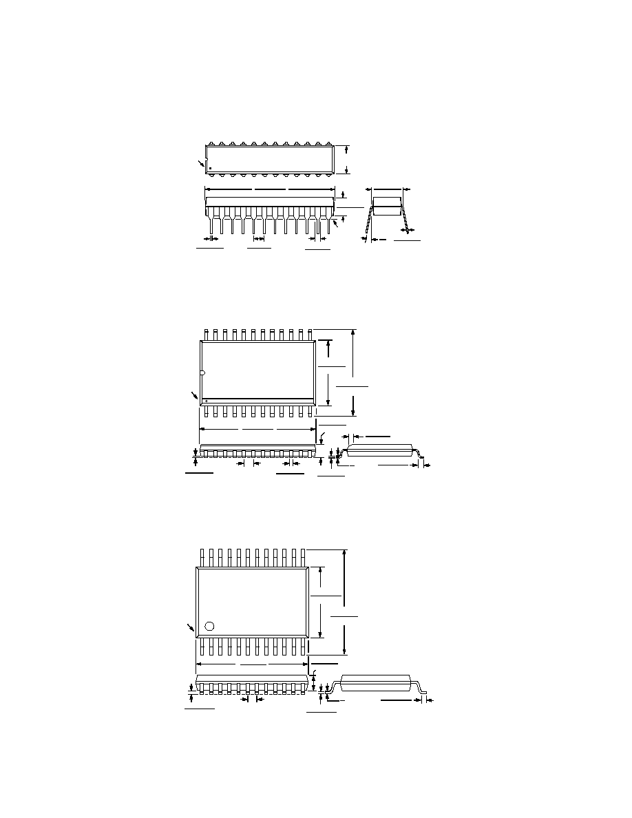
REV. B
≠34≠
AD7853/AD7853L
OUTLINE DIMENSIONS
Dimensions shown in inches and (mm).
24-Lead Plastic DIP
(N-24)
PIN 1
0.260
±
0.001
(6.61
±
0.03)
24
1
13
12
0.32 (8.128)
0.30 (7.62)
0.011 (0.28)
0.009 (0.23)
15
∞
0
0.02 (0.5)
0.016 (0.41)
0.130 (3.30)
0.128 (3.25)
0.07 (1.78)
0.05 (1.27)
SEATING
PLANE
1.228 (31.19)
1.226 (31.14)
0.11 (2.79)
0.09 (2.28)
NOTES
1. LEAD NO. 1 IDENTIFIED BY DOT OR NOTCH
2. PLASTIC LEADS WILL BE EITHER SOLDER DIPPED OR TIN PLATED
IN ACCORDANCE WITH MIL-M-38510 REQUIREMENTS.
24-Lead Small Outline Package
(R-24)
0.013 (0.32)
0.009 (0.23)
0.042 (1.067)
0.018 (0.447)
6
∞
0
∞
0.03 (0.76)
0.02 (0.51)
PIN 1
0.299 (7.6)
0.291 (7.39)
0.414 (10.52)
0.398 (10.10)
13
12
1
24
0.019 (0.49)
0.014 (0.35)
0.05 (1.27)
BSC
0.096 (2.44)
0.089 (2.26)
0.608 (15.45)
0.596 (15.13)
0.01 (0.254)
0.006 (0.15)
1. LEAD NO. 1 IDENTIFIED BY A DOT.
2. SOIC LEADS WILL BE EITHER TIN PLATED OR SOLDER DIPPED
IN ACCORDANCE WITH MIL-M-38510 REQUIREMENTS
24-Lead Shrink Small Outline Package
(RS-24)
1. LEAD NO. 1 IDENTIFIED BY A DOT.
2. LEADS WILL BE EITHER TIN PLATED OR SOLDER DIPPED
IN ACCORDANCE WITH MIL-M-38510 REQUIREMENTS
0.009 (0.229)
0.005 (0.127)
0.037 (0.94)
0.022 (0.559)
8
∞
0
∞
0.0256 (0.65)
BSC
0.07 (1.78)
0.066 (1.67)
0.328 (8.33)
0.318 (8.08)
0.008 (0.203)
0.002 (0.050)
PIN 1
0.311 (7.9)
0.301 (7.64)
0.212 (5.38)
0.205 (5.207)
1
24
13
12
PRINTED IN U.S.A.
C2024b≠2.5≠11/98