Äîêóìåíòàöèÿ è îïèñàíèÿ www.docs.chipfind.ru
a
Information furnished by Analog Devices is believed to be accurate and
reliable. However, no responsibility is assumed by Analog Devices for its
use, nor for any infringements of patents or other rights of third parties that
may result from its use. No license is granted by implication or otherwise
under any patent or patent rights of Analog Devices. Trademarks and
registered trademarks are the property of their respective companies.
One Technology Way, P.O. Box 9106, Norwood, MA 02062-9106, U.S.A.
Tel: 781/329-4700
www.analog.com
Fax: 781/326-8703
© 2002 Analog Devices, Inc. All rights reserved.
REV. 0
AD7923
4-Channel, 200 kSPS, 12-Bit ADC
with Sequencer in 16-Lead TSSOP
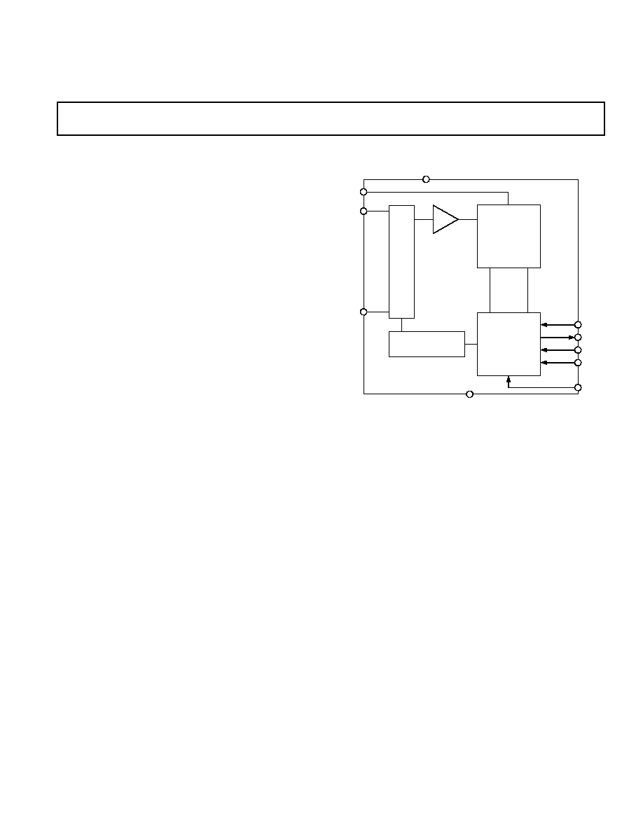
FUNCTIONAL BLOCK DIAGRAM
·
·
·
·
·
·
·
·
·
·
·
·
·
V
IN
3
T/H
I/P
MUX
SEQUENCER
CONTROL LOGIC
12-BIT
SUCCESSIVE
APPROXIMATION
ADC
GND
SCLK
DOUT
DIN
CS
V
DRIVE
AV
DD
AD7923
REF
IN
V
IN
0
FEATURES
Fast Throughput Rate: 200 kSPS
Specified for AV
DD
of 2.7 V to 5.25 V
Low Power:
3.6 mW Max at 200 kSPS with 3 V Supply
7.5 mW Max at 200 kSPS with 5 V Supply
4 (Single-Ended) Inputs with Sequencer
Wide Input Bandwidth:
70 dB Min SNR at 50 kHz Input Frequency
Flexible Power/Serial Clock Speed Management
No Pipeline Delays
High Speed Serial Interface SPITM/QSPITM/
MICROWIRETM/DSP Compatible
Shutdown Mode: 0.5 A Max
16-Lead TSSOP Package
GENERAL DESCRIPTION
The AD7923 is a 12-bit, high speed, low power, 4-channel,
successive approximation ADC. The part operates from a single
2.7 V to 5.25 V power supply and features throughput rates up
to 200 kSPS. The part contains a low noise, wide bandwidth
track-and-hold amplifier that can handle input frequencies in
excess of 8 MHz.
The conversion process and data acquisition are controlled using
CS and the serial clock signal, allowing the device to easily
interface with microprocessors or DSPs. The input signal is
sampled on the falling edge of
CS and the conversion is also
initiated at this point. There are no pipeline delays associated
with the part.
The AD7923 uses advanced design techniques to achieve very low
power dissipation at maximum throughput rates. At maximum
throughput rates, the AD7923 consumes 1.2 mA maximum with 3 V
supplies, and with 5 V supplies the current consumption is 1.5 mA
maximum.
Through the configuration of the Control Register, the analog
input range for the part can be selected as 0 V to REF
IN
or 0 V
to 2
¥ REF
IN
, with either straight binary or twos complement
output coding. The AD7923 features four single-ended analog
inputs with a channel sequencer to allow a preprogrammed
selection of channels to be converted sequentially.
The conversion time for the AD7923 is determined by the SCLK
frequency, as this is also used as the master clock to control the
conversion. The conversion time may be as short as 800 ns with
a 20 MHz SCLK.
PRODUCT HIGHLIGHTS
1. High Throughput with Low Power Consumption.
The AD7923 offers up to 200 kSPS throughput rates. At the
maximum throughput rate with 3 V supplies, the AD7923
dissipates just 3.6 mW of power maximum.
2. Four Single-Ended Inputs with a Channel Sequencer.
A consecutive sequence of channels, through which the ADC
will cycle and convert on, can be selected.
3. Single-Supply Operation with V
DRIVE
Function.
The AD7923 operates from a single 2.7 V to 5.25 V supply.
The V
DRIVE
function allows the serial interface to connect
directly to either 3 V or 5 V processor systems independent of AV
DD
.
4. Flexible Power/Serial Clock Speed Management.
The conversion rate is determined by the serial clock, allowing
the conversion time to be reduced through the serial clock speed
increase. The part also features various shutdown modes to
maximize power efficiency at lower throughput rates. Current
consumption is 0.5
mA maximum when in full shutdown.
5. No Pipeline Delay.
The part features a standard successive approximation ADC
with accurate control of the sampling instant via a
CS input
and once off conversion control.

2
REV. 0
(AV
DD
= V
DRIVE
= 2.7 V to 5.25 V, REF
IN
= 2.5 V, f
SCLK
= 20 MHz, T
A
= T
MIN
to T
MAX
,
unless otherwise noted.)
Parameter
B Version
1
Unit
Test Conditions/Comments
DYNAMIC PERFORMANCE
f
IN
= 50 kHz Sine Wave, f
SCLK
= 20 MHz
Signal-to-(Noise + Distortion) (SINAD)
2
70
dB min
@ 5 V
69
dB min
@ 3 V Typically 70 dB
Signal-to-Noise Ratio (SNR)
2
70
dB min
Total Harmonic Distortion (THD)
2
77
dB max
@ 5 V Typically 84 dB
73
dB max
@ 3 V Typically 77 dB
Peak Harmonic or Spurious Noise
78
dB max
@ 5 V Typically 86 dB
(SFDR)
2
76
dB max
@ 3 V Typically 80 dB
Intermodulation Distortion (IMD)
2
fa = 40.1 kHz, fb = 41.5 kHz
Second Order Terms
90
dB typ
Third Order Terms
90
dB typ
Aperture Delay
10
ns typ
Aperture Jitter
50
ps typ
Channel-to-Channel Isolation
2
85
dB typ
f
IN
= 400 kHz
Full Power Bandwidth
8.2
MHz typ
@ 3 dB
1.6
MHz typ
@ 0.1 dB
DC ACCURACY
2
Resolution
12
Bits
Integral Nonlinearity
±1
LSB max
Differential Nonlinearity
0.9/+1.5
LSB max
Guaranteed No Missed Codes to 12 Bits.
0 V to REF
IN
Input Range
Straight Binary Output Coding
Offset Error
±8
LSB max
Typically
±0.5 LSB
Offset Error Match
±0.5
LSB max
Gain Error
±1.5
LSB max
Gain Error Match
±0.5
LSB max
0 V to 2
¥ REF
IN
Input Range
REF
IN
to +REF
IN
Biased about REF
IN
with
Positive Gain Error
±1.5
LSB max
Twos Complement Output Coding
Positive Gain Error Match
±0.5
LSB max
Zero Code Error
±8
LSB max
Typically
±0.8 LSB
Zero Code Error Match
±0.5
LSB max
Negative Gain Error
±1
LSB max
Negative Gain Error Match
±0.5
LSB max
ANALOG INPUT
Input Voltage Range
0 to REF
IN
V
RANGE Bit Set to 1
0 to 2
¥ REF
IN
V
RANGE Bit Set to 0, AV
DD
/V
DRIVE
= 4.75 V to 5.25 V
DC Leakage Current
±1
mA max
Input Capacitance
20
pF typ
REFERENCE INPUT
REF
IN
Input Voltage
2.5
V
±1% Specified Performance
DC Leakage Current
±1
mA max
REF
IN
Input Impedance
36
k
W typ
f
SAMPLE
= 200 kSPS
LOGIC INPUTS
Input High Voltage, V
INH
0.7
¥ V
DRIVE
V min
Input Low Voltage, V
INL
0.3
¥ V
DRIVE
V max
Input Current, I
IN
±1
mA max
Typically 10 nA, V
IN
= 0 V or V
DRIVE
Input Capacitance, C
IN
3
10
pF max
LOGIC OUTPUTS
Output High Voltage, V
OH
V
DRIVE
0.2
V min
I
SOURCE
= 200
mA, AV
DD
= 2.7 V to 5.25 V
Output Low Voltage, V
OL
0.4
V max
I
SINK
= 200
mA
Floating-State Leakage Current
±1
mA max
Floating-State Output Capacitance
3
10
pF max
Output Coding
Straight (Natural) Binary
Coding Bit Set to 1
Twos Complement
Coding Bit Set to 0
AD7923SPECIFICATIONS

AD7923
3
REV. 0
Parameter
B Version
1
Unit
Test Conditions/Comments
CONVERSION RATE
Conversion Time
800
ns max
16 SCLK Cycles with SCLK at 20 MHz
Track-and-Hold Acquisition Time
300
ns max
Sine Wave Input
300
ns max
Full-Scale Step Input
Throughput Rate
200
kSPS max
See Serial Interface Section
POWER REQUIREMENTS
AV
DD
2.7/5.25
V min/max
V
DRIVE
2.7/5.25
V min/max
I
DD
4
Digital I/Ps = 0 V or V
DRIVE
During Conversion
2.7
mA max
AV
DD
= 4.75 V to 5.25 V, f
SCLK
= 20 MHz
2.0
mA max
AV
DD
= 2.7 V to 3.6 V, f
SCLK
= 20 MHz
Normal Mode (Static)
600
mA typ
AV
DD
= 2.7 V to 5.25 V, SCLK On or Off
Normal Mode (Operational) f
SAMPLE
= 200 kSPS
1.5
mA max
AV
DD
= 4.75 V to 5.25 V, f
SCLK
= 20 MHz
1.2
mA max
AV
DD
= 2.7 V to 3.6 V, f
SCLK
= 20 MHz
Using Auto Shutdown Mode f
SAMPLE
= 200 kSPS
900
mA typ
AV
DD
= 4.75 V to 5.25 V, f
SAMPLE
= 200 kSPS
650
mA typ
AV
DD
= 2.7 V to 3.6 V, f
SAMPLE
= 200 kSPS
Auto Shutdown (Static)
0.5
mA max
SCLK On or Off (20 nA typ)
Full Shutdown Mode
0.5
mA max
SCLK On or Off (20 nA typ)
Power Dissipation
4
Normal Mode (Operational) f
SAMPLE
= 200 kSPS
7.5
mW max
AV
DD
= 5 V, f
SCLK
= 20 MHz
3.6
mW max
AV
DD
= 3 V, f
SCLK
= 20 MHz
Auto Shutdown (Static)
2.5
mW max
AV
DD
= 5 V
1.5
mW max
AV
DD
= 3 V
Full Shutdown Mode
2.5
mW max
AV
DD
= 5 V
1.5
mW max
AV
DD
= 3 V
NOTES
1
Temperature ranges as follows: B Version: 40
C to +85C.
2
See Terminology section.
3
Sample tested @ 25
C to ensure compliance.
4
See Power versus Throughput Rate section.
Specifications subject to change without notice.
4
AD7923
REV. 0
TIMING SPECIFICATIONS
1
(AV
DD
= 2.7 V to 5.25 V, V
DRIVE
AV
DD
, REF
IN
= 2.5 V, T
A
= T
MIN
to T
MAX
, unless otherwise noted.)
Limit at T
MIN
, T
MAX
AD7923
Parameter
AV
DD
= 3 V
AV
DD
= 5 V
Unit
Description
f
SCLK
2
10
10
kHz min
20
20
MHz max
t
CONVERT
16
¥ t
SCLK
16
¥ t
SCLK
t
QUIET
50
50
ns min
Minimum Quiet Time Required between
CS Rising
Edge and Start of Next Conversion
t
2
10
10
ns min
CS to SCLK Setup Time
t
3
3
35
30
ns max
Delay from
CS until DOUT Three-State Disabled
t
4
3
40
40
ns max
Data Access Time after SCLK Falling Edge
t
5
0.4
¥ t
SCLK
0.4
¥ t
SCLK
ns min
SCLK Low Pulsewidth
t
6
0.4
¥ t
SCLK
0.4
¥ t
SCLK
ns min
SCLK High Pulsewidth
t
7
10
10
ns min
SCLK to DOUT Valid Hold Time
t
8
4
15/45
15/35
ns min/max
SCLK Falling Edge to DOUT High Impedance
t
9
10
10
ns min
DIN Setup Time Prior to SCLK Falling Edge
t
10
5
5
ns min
DIN Hold Time after SCLK Falling Edge
t
11
20
20
ns min
Sixteenth SCLK Falling Edge to
CS High
t
12
1
1
ms max
Power-Up Time from Full Power-Down/Auto
Shutdown Mode
NOTES
1
Sample tested at 25
C to ensure compliance. All input signals are specified with t
R
= t
F
= 5 ns (10% to 90% of AV
DD
) and timed from a voltage level of 1.6 V.
See Figure 1. The 3 V operating range spans from 2.7 V to 3.6 V. The 5 V operating range spans from 4.75 V to 5.25 V.
2
Mark/Space ratio for the SCLK input is 40/60 to 60/40.
3
Measured with the load circuit of Figure 1 and defined as the time required for the output to cross 0.4 V or 0.7
¥ V
DRIVE
.
4
t
8
is derived from the measured time taken by the data outputs to change 0.5 V when loaded with the circuit of Figure 1. The measured number is then extrapolated
back to remove the effects of charging or discharging the 50 pF capacitor. This means that the time, quoted in the timing characteristics t
8
, is the true bus relinquish
time of the part and is independent of the bus loading.
Specifications subject to change without notice.
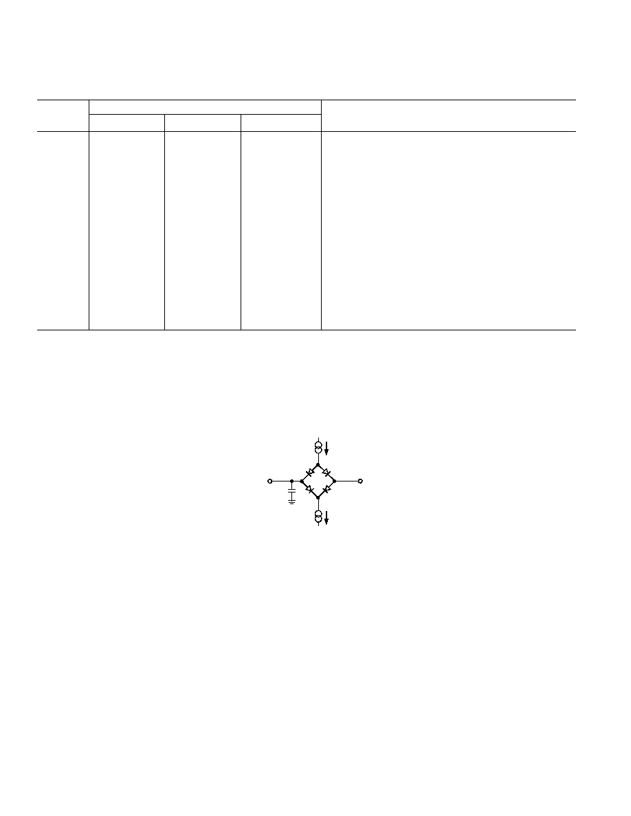
TO
OUTPUT
PIN
C
L
50pF
200 A
I
OH
200 A
I
OL
1.6V
Figure 1. Load Circuit for Digital Output Timing Specifications

AD7923
5
REV. 0
ABSOLUTE MAXIMUM RATINGS
1
(T
A
= 25
C, unless otherwise noted.)
AV
DD
to AGND . . . . . . . . . . . . . . . . . . . . . . . 0.3 V to +7 V
V
DRIVE
to AGND . . . . . . . . . . . . . . . . 0.3 V to AV
DD
+ 0.3 V
Analog Input Voltage to AGND . . . . 0.3 V to AV
DD
+ 0.3 V
Digital Input Voltage to AGND . . . . . . . . . . . . 0.3 V to +7 V
Digital Output Voltage to AGND . . . . 0.3 V to AV
DD
+ 0.3 V
REF
IN
to AGND . . . . . . . . . . . . . . . . 0.3 V to AV
DD
+ 0.3 V
Input Current to Any Pin Except Supplies
2
. . . . . . . .
±10 mA
Operating Temperature Range
Commercial (B Version) . . . . . . . . . . . . . . 40
C to +85C
Storage Temperature Range . . . . . . . . . . . 65
C to +150C
Junction Temperature . . . . . . . . . . . . . . . . . . . . . . . . . 150
C
TSSOP Package, Power Dissipation . . . . . . . . . . . . . 450 mW
q
JA
Thermal Impedance . . . . . . . . . . . . 150.4
C/W (TSSOP)
q
JC
Thermal Impedance . . . . . . . . . . . . . 27.6
C/W (TSSOP)
Lead Temperature, Soldering
Vapor Phase (60 sec) . . . . . . . . . . . . . . . . . . . . . . . . 215
C
Infrared (15 sec) . . . . . . . . . . . . . . . . . . . . . . . . . . . 220
C
ESD . . . . . . . . . . . . . . . . . . . . . . . . . . . . . . . . . . . . . . . . . 2 kV
NOTES
1
Stresses above those listed under Absolute Maximum Ratings may cause perma-
nent damage to the device. This is a stress rating only and functional operation of
the device at these or any other conditions above those listed in the operational
sections of this specification is not implied. Exposure to absolute maximum rating
conditions for extended periods may affect device reliability.
2
Transient currents of up to 100 mA will not cause SCR latch-up.
CAUTION
ESD (electrostatic discharge) sensitive device. Electrostatic charges as high as 4000 V readily
accumulate on the human body and test equipment and can discharge without detection. Although the
AD7923 features proprietary ESD protection circuitry, permanent damage may occur on devices
subjected to high energy electrostatic discharges. Therefore, proper ESD precautions are recommended
to avoid performance degradation or loss of functionality.
ORDERING GUIDE
Temperature
Linearity
Package
Package
Model
Range
Error (LSB)
1
Option
Description
AD7923BRU
40
C to +85C
±1
RU-16
TSSOP
EVAL-AD7923CB
2
Evaluation Board
EVAL-CONTROL BRD2
3
Controller Board
NOTES
1
Linearity error here refers to integral linearity error.
2
This can be used as a standalone evaluation board or in conjunction with the Evaluation Controller Board for evaluation/demonstration purposes.
3
This board is a complete unit allowing a PC to control and communicate with all Analog Devices evaluation boards ending in the CB designators.
To order a complete evaluation kit, the you will need to order the particular ADC evaluation board, e.g., EVAL-AD7923CB, the EVAL-CONTROL
BRD2, and a 12 V ac transformer. See the relevant Evaluation Board Application Note for more information.
6
AD7923
REV. 0
PIN FUNCTION DESCRIPTIONS
Pin No.
Mnemonic
Function
1
SCLK
Serial Clock. Logic Input. SCLK provides the serial clock for accessing data for the part. This clock
input is also used as the clock source for the AD7923 conversion process.
2
DIN
Data In. Logic Input. Data to be written to the AD7923 Control Register is provided on this input and is
clocked into the register on the falling edge of SCLK (see the Control Register section).
3
CS
Chip Select. Active low logic input. This input provides the dual function of initiating conversions on
the AD7923 and framing the serial data transfer.
4, 8, 13, 16
AGND
Analog Ground. Ground reference point for all analog circuitry on the AD7923. All analog input
signals and any external reference signal should be referred to this AGND voltage. All AGND pins
should be connected together.
5, 6
AV
DD
Analog Power Supply Input. The AV
DD
range for the AD7923 is from 2.7 V to 5.25 V. For the
0 V to 2
¥ REF
IN
range, AV
DD
should be from 4.75 V to 5.25 V.
7
REF
IN
Reference Input for the AD7923. An external reference must be applied to this input. The voltage
range for the external reference is 2.5 V
±1% for specified performance.
129
V
IN
0V
IN
3
Analog Input 0 through Analog Input 3. Four single-ended analog input channels that are multiplexed
into the on-chip track-and-hold. The analog input channel to be converted is selected by using the
address bits ADD1 and ADD0 of the Control Register. The address bits in conjunction with the SEQ1
and SEQ0 bits allow the sequencer to be programmed. The input range for all input channels can extend
from 0 V to REF
IN
or from 0 V to 2
¥ REF
IN
as selected via the RANGE bit in the Control Register.
Any unused input channels must be connected to AGND to avoid noise pickup.
14
DOUT
Data Out. Logic Output. The conversion result from the AD7923 is provided on this output as a serial
data stream. The bits are clocked out on the falling edge of the SCLK input. The data stream from the
AD7923 consists of two leading zeros, two address bits indicating which channel the conversion result
corresponds to, followed by the 12 bits of conversion data, MSB first. The output coding may be
selected as straight binary or twos complement via the CODING bit in the Control Register.
15
V
DRIVE
Logic Power Supply Input. The voltage supplied at this pin determines at which voltage the serial interface
of the AD7923 will operate.
PIN CONFIGURATION
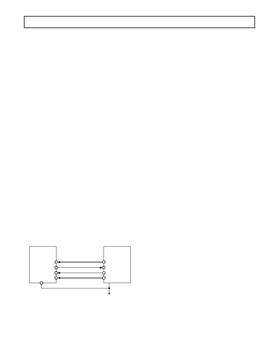
16-Lead TSSOP
1
AD7923
SCLK
AGND
16
TOP VIEW
(Not to Scale)
2
DIN
V
DRIVE
15
3
CS
DOUT
14
4
AGND
AGND
13
5
AV
DD
V
IN
0
12
6
AV
DD
V
IN
1
11
7
REF
IN
V
IN
2
10
8
AGND
V
IN
3
9

AD7923
7
REV. 0
TERMINOLOGY
Integral Nonlinearity
This is the maximum deviation from a straight line passing
through the endpoints of the ADC transfer function. The end-
points of the transfer function are zero-scale, a point 1 LSB
below the first code transition, and full-scale, a point 1 LSB
above the last code transition.
Differential Nonlinearity
This is the difference between the measured and the ideal 1 LSB
change between any two adjacent codes in the ADC.
Offset Error
This is the deviation of the first code transition (00 . . . 000) to
(00 . . . 001) from the ideal, i.e., AGND + 1 LSB.
Offset Error Match
This is the difference in offset error between any two channels.
Gain Error
This is the deviation of the last code transition (111 . . . 110) to
(111 . . . 111) from the ideal (i.e., REF
IN
1 LSB) after the
offset error has been adjusted out.
Gain Error Match
This is the difference in Gain Error between any two channels.
Zero Code Error
This applies when using the twos complement output coding
option, in particular to the 2
¥ REF
IN
input range with REF
IN
to +REF
IN
biased about the REF
IN
point. It is the deviation of
the midscale transition (all 0s to all 1s) from the ideal V
IN
voltage,
i.e., REF
IN
1 LSB.
Zero Code Error Match
This is the difference in Zero Code Error between any two
channels.
Positive Gain Error
This applies when using the twos complement output coding
option, in particular to the 2
¥ REF
IN
input range with REF
IN
to +REF
IN
biased about the REF
IN
point. It is the deviation of
the last code transition (011. . .110) to (011 . . . 111) from the
ideal (i.e., +REF
IN
1 LSB) after the Zero Code Error has been
adjusted out.
Positive Gain Error Match
This is the difference in Positive Gain Error between any two
channels.
Negative Gain Error
This applies when using the twos complement output coding
option, in particular to the 2
¥ REF
IN
input range with REF
IN
to +REF
IN
biased about the REF
IN
point. It is the deviation of
the first code transition (100 . . . 000) to (100 . . . 001) from the
ideal (i.e., REF
IN
+ 1 LSB) after the Zero Code Error has been
adjusted out.
Negative Gain Error Match
This is the difference in Negative Gain Error between any two
channels.
Channel-to-Channel Isolation
Channel-to-Channel Isolation is a measure of the level of crosstalk
between channels. It is measured by applying a full-scale 400 kHz
sine wave signal to all three nonselected input channels and
determining how much that signal is attenuated in the selected
channel with a 50 kHz signal. The figure is given worst-case
across all four channels for the AD7923.
PSR (Power Supply Rejection)
Variations in power supply will affect the full-scale transition,
but not the converter's linearity. Power supply rejection is the
maximum change in full-scale transition point due to a change
in power supply voltage from the nominal value. See Typical
Performance Characteristics.
Track-and-Hold Acquisition Time
The track-and-hold amplifier returns into track mode at the end
of conversion. Track-and-hold acquisition time is the time
required for the output of the track-and-hold amplifier to reach
its final value, within
±1 LSB, after the end of conversion.
Signal-to-(Noise + Distortion) Ratio
This is the measured ratio of signal-to-(noise + distortion) at the
output of the A/D converter. The signal is the rms amplitude of
the fundamental. Noise is the sum of all nonfundamental sig-
nals up to half the sampling frequency (f
S
/2), excluding dc. The
ratio is dependent on the number of quantization levels in the
digitization process; the more levels, the smaller the quantiza-
tion noise. The theoretical signal-to-(noise + distortion) ratio
for an ideal N-bit converter with a sine wave input is given by:
Signal to Noise
Distortion
N
dB
- -(
)
( .
.
)
+
=
+
6 02
1 76
Thus for a 12-bit converter, this is 74 dB.
Total Harmonic Distortion (THD)
Total harmonic distortion (THD) is the ratio of the rms sum of
harmonics to the fundamental. For the AD7923, it is defined as:
THD dB
V
V
V
V
V
V
(
)
log
=
+
+
+
+
20
2
2
3
2
4
2
5
2
6
2
1
where V
1
is the rms amplitude of the fundamental and V
2
, V
3
,
V
4
, V
5
, and V
6
are the rms amplitudes of the second through the
sixth harmonics.
8
AD7923Typical Performance Characteristics
REV. 0
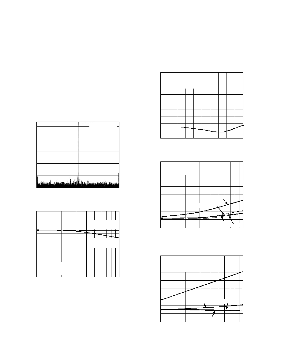
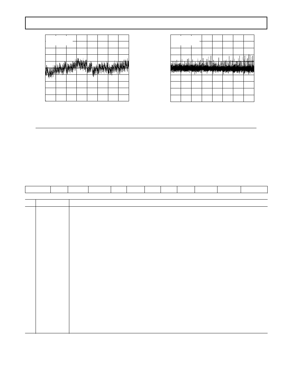
PERFORMANCE CURVES
TPC 1 shows a typical FFT plot for the AD7923 at 200 kSPS
sample rate and 50 kHz input frequency. TPC 2 shows the
signal-to-(noise+distortion) ratio performance versus input
frequency for various supply voltages while sampling at 200 kSPS
with an SCLK of 20 MHz.
TPC 3 shows the power supply rejection ratio versus supply
ripple frequency for the AD7923 with no decoupling. The power
supply rejection ratio is defined as the ratio of the power in the
ADC output at full-scale frequency f, to the power of a 200 mV
p-p sine wave applied to the ADC AV
DD
supply of frequency f
S
:
PSRR dB
Pf Pf
s
(
)
log(
/
)
= 10
Pf is equal to the power at frequency f in ADC output; Pf
S
is equal
to the power at frequency f
S
coupled onto the ADC AV
DD
supply.
Here a 200 mV p-p sine wave is coupled onto the AV
DD
supply.
TPC 4 shows a graph of total harmonic distortion versus analog
input frequency for various supply voltages, while TPC 5 shows
a graph of total harmonic distortion versus analog input frequency
for various source impedances. See the Analog Input section.
TPC 6 and TPC 7 show typical INL and DNL plots for the
AD7923.
FREQUENCY kHz
10
0
20
40
60
80
100
SNR dB
30
50
70
90
110
10
30
50
70
90
4096 POINT FFT
AV
DD
= 4.75V
f
SAMPLE
= 200kSPS
f
IN
= 50kHz
SINAD = 70.714dB
THD = 82.853dB
SFDR = 84.815dB
TPC 1. Dynamic Performance at 200 kSPS
INPUT FREQUENCY kHz
75
0
100
SINAD dB
70
65
60
f
SAMPLE
= 200kSPS
T
A
= 25 C
RANGE = 0 V TO REF
IN
AV
DD
= V
DRIVE
= 5.25V
AV
DD
= V
DRIVE
= 4.75V
AV
DD
= V
DRIVE
= 3.6V
AV
DD
= V
DRIVE
= 2.7V
TPC 2. SINAD vs. Analog Input Frequency for Various
Supply Voltages at 200 kSPS
SUPPLY RIPPLE FREQUENCY kHz
0
0
200
PSRR dB
40
60
80
90
100
20
50
70
180
160
140
120
80
60
40
20
AV
DD
= 5V,
200mV p-p SINE WAVE ON AV
DD
REF
IN
= 2.5V, 1 F CAPACITOR
T
A
= 25 C
10
30
TPC 3. PSRR vs. Supply Ripple Frequency
INPUT FREQUENCY kHz
50
10
100
THD dB
65
75
85
90
55
70
80
f
SAMPLE
= 200kSPS
T
A
= 25 C
RANGE = 0V TO REF
IN
60
AV
DD
= V
DRIVE
= 2.7V
AV
DD
= V
DRIVE
= 3.6V
AV
DD
= V
DRIVE
= 4.75V
AV
DD
= V
DRIVE
= 5.25V
TPC 4. THD vs. Analog Input Frequency for Various
Supply Voltages at 200 kSPS
INPUT FREQUENCY kHz
55
10
100
THD dB
70
80
90
95
60
75
85
f
SAMPLE
= 200kSPS
T
A
= 25 C
AV
DD
= 5.25V
RANGE = 0V TO REF
IN
65
R
IN
= 50
R
IN
= 100
R
IN
= 10
R
IN
= 1000
TPC 5. THD vs. Analog Input Frequency for Various
Source Impedances
AD7923
9
REV. 0
Table I. Control Register Bit Functions
MSB
LSB
WRITE
SEQ1 DONTC
DONTC
ADD1 ADD0
PM1
PM0
SEQ0
DONTC
RANGE
CODING
Bit
Mnemonic
Comment
11
WRITE
The value written to this bit of the Control Register determines whether the following 11 bits will be
loaded to the Control Register. If this bit is a 1, the following 11 bits will be written to the Control Register;
if it is a 0, the remaining 11 bits are not loaded to the Control Register and it remains unchanged.
10
SEQ1
The SEQ1 bit in the Control Register is used in conjunction with the SEQ0 bit to control the use of the
sequencer function. (See Table IV.)
98
DONTC
Don't Care
76
ADD1, ADD0 These two address bits are loaded at the end of the present conversion and select which analog input channel is to
be converted in the next serial transfer, or they may select the final channel in a consecutive sequence as described
in Table IV. The selected input channel is decoded as shown in Table II. The address bits corresponding to
the conversion result are also output on DOUT prior to the 12 bits of data. (See the Serial Interface section.)
The next channel to be converted on will be selected by the mux on the 14th SCLK falling edge.
5, 4
PM1, PM0
Power Management Bits. These two bits decode the mode of operation of the AD7923 as shown in Table III.
3
SEQ0
The SEQ0 bit in the Control Register is used in conjunction with the SEQ1 bit to control the use of the
sequencer function. (See Table IV.)
2
DONTC
Don't Care
1
RANGE
This bit selects the analog input range to be used on the AD7923. If it is set to 0, the analog input range
will extend from 0 V to 2
¥ REF
IN
. If it is set to 1, the analog input range will extend from 0 V to REF
IN
(for
the next conversion). For the 0 V to 2
¥ REF
IN
range, AV
DD
= 4.75 V to 5.25 V.
0
CODING
This bit selects the type of output coding the AD7923 will use for the conversion result. If this bit is set to 0,
the output coding for the part will be twos complement. If this bit is set to 1, the output coding from the
part will be straight binary (for the next conversion).
CODE
1.0
0
4096
INL ERR
OR LSB
0
0.4
0.8
1.0
0.2
0.2
0.6
2048
0.6
AV
DD
= V
DRIVE
= 5V
TEMP = 25 C
0.4
0.8
2560
3072
3584
512
1024
1536
TPC 6. Typical INL
CONTROL REGISTER
The Control Register on the AD7923 is a 12-bit, write-only register. Data is loaded from the DIN pin of the AD7923 on the falling
edge of SCLK. The data is transferred on the DIN line at the same time that the conversion result is read from the part. The data
transferred on the DIN line corresponds to the AD7923 configuration for the next conversion. This requires 16 serial clocks for every
data transfer. Only the information provided on the first 12 falling clock edges (after
CS falling edge) is loaded to the Control Register.
MSB denotes the first bit in the data stream. The bit functions are outlined in Table I.
CODE
1.0
0
4096
DNL ERR
OR LSB
0
0.4
0.8
1.0
0.2
0.2
0.6
2048
0.6
0.4
0.8
2560
3072
3584
512
1024
1536
AV
DD
= V
DRIVE
= 5V
TEMP = 25 C
TPC 7. Typical DNL

10
AD7923
REV. 0
Table III. Power Mode Selection
PM1 PM0 Mode
1
1
Normal Operation. In this mode, the AD7923 remains in full power mode, regardless of the status of any of the logic
inputs. This mode allows the fastest possible throughput rate from the AD7923.
1
0
Full Shutdown. In this mode, the AD7923 is in full shutdown mode with all circuitry on the AD7923 powering down.
The AD7923 retains the information in the Control Register while in full shutdown. The part remains in full shutdown
until these bits are changed.
0
1
Auto Shutdown. In this mode, the AD7923 automatically enters full shutdown mode at the end of each conversion
when the Control Register is updated. Wake-up time from full shutdown is 1
ms, and the user should ensure that 1 ms has
elapsed before attempting to perform a valid conversion on the part in this mode.
0
0
Invalid Selection. This configuration is not allowed.
SEQUENCER OPERATION
The configuration of the SEQ1 and SEQ0 bits in the Control
Register allows the user to select a particular mode of operation
of the sequencer function. Table IV outlines the three modes of
operation of the sequencer.
Table IV. Sequence Selection
SEQ1 SEQ0 Sequence Type
0
X
This configuration means that the sequence function is not used. The analog input channel selected for each
individual conversion is determined by the contents of the channel address bits ADD1, ADD0 in each prior write
operation. This mode of operation reflects the traditional operation of a multichannel ADC, without the sequencer
function being used, where each write to the AD7923 selects the next channel for conversion. (See Figure 2.)
1
0
If the SEQ1 and SEQ0 bits are set in this way, the sequence function will not be interrupted upon completion of the
WRITE operation. This allows other bits in the Control Register to be altered between conversions while in a
sequence without terminating the cycle.
1
1
This configuration is used in conjunction with the channel address bits ADD1, ADD0 to program continuous
conversions on a consecutive sequence of channels from Channel 0 to a selected final channel as determined by the
channel address bits in the Control Register. (See Figure 3.)
Table II. Channel Selection
ADD1
ADD0
Analog Input Channel
0
0
V
IN
0
0
1
V
IN
1
1
0
V
IN
2
1
1
V
IN
3
AD7923
11
REV. 0
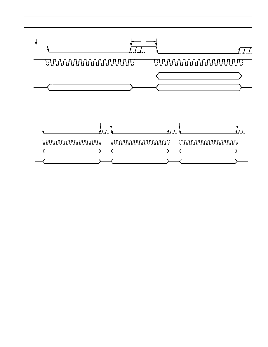
Figure 2 reflects the traditional operation of a multichannel ADC,
where each serial transfer selects the next channel for conversion.
In this mode of operation the Sequencer function is not used.
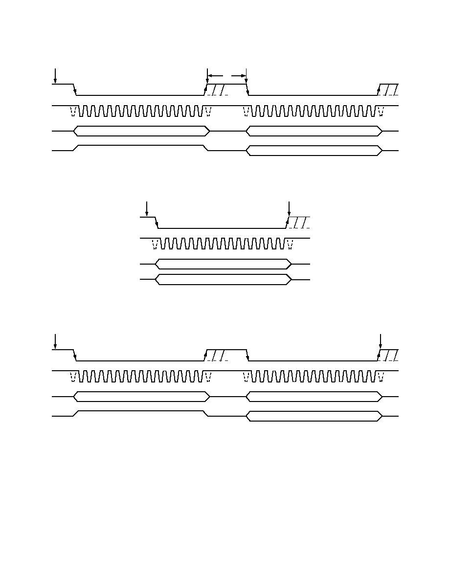
Figure 3 shows how to program the AD7923 to continuously
convert on a sequence of consecutive channels from Channel 0
to a selected final channel. To exit this mode of operation and
revert back to the traditional mode of operation of a multichannel
ADC (as outlined in Figure 2), ensure that the WRITE bit = 1
and SEQ1 = SEQ0 = 0 on the next serial transfer.
POWER-ON
DUMMY CONVERSION
DIN: WRITE TO CONTROL REGISTER,
WRITE BIT = 1,
SELECT CODING, RANGE, AND POWER MODE.
SELECT CHANNEL A1, A0 FOR CONVERSION.
SEQ1 = 0, SEQ0 = x
DOUT: CONVERSION RESULT FROM PREVIOUSLY
SELECTED CHANNEL A1, A0
DIN: WRITE TO CONTROL REGISTER,
WRITE BIT = 1,
SELECT CODING, RANGE, AND POWER MODE.
SELECT A1, A0 FOR CONVERSION.
SEQ1 = 0, SEQ0 = x
WRITE BIT = 1,
SEQ1 = 0,
SEQ0 = x
CS
CS
Figure 2. SEQ1 Bit = 0, SEQ0 Bit = x Flowchart
POWER-ON
DUMMY CONVERSION
DIN: WRITE TO CONTROL REGISTER,
WRITE BIT = 1,
SELECT CODING, RANGE, AND POWER MODE.
SELECT CHANNEL A1, A0 FOR CONVERSION.
SEQ1 = 1, SEQ0 = 1
DOUT: CONVERSION RESULT FROM CHANNEL 0
CONTINUOUSLY CONVERTS ON A CONSECUTIVE
SEQUENCE OF CHANNELS FROM CHANNEL 0 UP
TO AND INCLUDING THE PREVIOUSLY SELECTED
A1, A0 IN THE CONTROL REGISTER
WRITE BIT = 0
CONTINUOUSLY CONVERTS ON THE SELECTED
SEQUENCE OF CHANNELS BUT WILL ALLOW
RANGE, CODING, ETC., TO CHANGE IN THE CON-
TROL REGISTER WITHOUT INTERRUPTING THE
SEQUENCE, PROVIDED SEQ = 1, SEQ0 = 0
WRITE BIT = 1,
SEQ1 = 1,
SEQ0 = 0
CS
CS
CS
Figure 3. SEQ1 Bit = 1, SEQ0 Bit = 1 Flowchart
CIRCUIT INFORMATION
The AD7923 is high speed, 4-channel, 12-bit, single-supply
A/D converter. The part can be operated from a 2.7 V to 5.25 V
supply. When operated from either a 5 V or 3 V supply, the
AD7923 is capable of throughput rates of 200 kSPS. The con-
version time may be as short as 800 ns when provided with a
20 MHz clock.
The AD7923 provides the user with an on-chip, track-and-hold
A/D converter, and with a serial interface housed in a 16-lead
TSSOP package. The AD7923 has four single-ended input
channels with a channel sequencer, allowing the user to select a
channel sequence through which the ADC can cycle with each
consecutive
CS falling edge. The serial clock input accesses data
from the part, controls the transfer of data written to the ADC,
and provides the clock source for the successive approximation
A/D converter. The analog input range for the AD7923 is 0 V
to REF
IN
or 0 V to 2
¥ REF
IN
, depending on the status of Bit 1
in the Control Register. For the 0 to 2
¥ REF
IN
range, the part
must be operated from a 4.75 V to 5.25 V supply.
The AD7923 provides flexible power management options to
allow the user to achieve the best power performance for a given
throughput rate. These options are selected by programming the
Power Management bits, PM1 and PM0, in the Control Register.
CONVERTER OPERATION
The AD7923 is a 12-bit successive approximation analog-to-
digital converter based around a capacitive DAC. The AD7923
can convert analog input signals in the range 0 V to REF
IN
or 0 V
to 2
¥ REF
IN
. Figures 4 and 5 show simplified schematics of the
ADC. The ADC is comprised of Control Logic, SAR, and a
capacitive DAC, which are used to add and subtract fixed amounts
of charge from the sampling capacitor to bring the comparator
back into a balanced condition. Figure 4 shows the ADC during
its acquisition phase. SW2 is closed and SW1 is in position A. The
comparator is held in a balanced condition and the sampling
capacitor acquires the signal on the selected V
IN
channel.
V
IN
0
V
IN
3
AGND
A
B
SW1
SW2
COMPARATOR
CONTROL
LOGIC
CAPACITIVE
DAC
4k
Figure 4. ADC Acquisition Phase
12
AD7923
REV. 0
When the ADC starts a conversion (see Figure 5), SW2 will
open and SW1 will move to position B, causing the comparator
to become unbalanced. The Control Logic and the capacitive
DAC are used to add and subtract fixed amounts of charge from
the sampling capacitor to bring the comparator back into a
balanced condition. When the comparator is rebalanced, the
conversion is complete. The Control Logic generates the ADC
output code. Figures 7 and 8 show the ADC transfer functions.
V
IN
0
.
.
V
IN
3
AGND
A
B
SW1
SW2
COMPARATOR
CONTROL
LOGIC
4k
CAPACITIVE
DAC
Figure 5. ADC Conversion Phase
Analog Input
Figure 6 shows an equivalent circuit of the analog input struc-
ture of the AD7923. The two diodes D1 and D2 provide ESD
protection for the analog inputs. Care must be taken to ensure
that the analog input signal never exceeds the supply rails by
more than 200 mV. This will cause these diodes to become
forward-biased and start conducting current into the substrate.
10 mA is the maximum current these diodes can conduct with-
out causing irreversible damage to the part. Capacitor C1 in
Figure 6 is typically about 4 pF and can primarily be attributed
to pin capacitance. The resistor R1 is a lumped component
made up of the on resistance of the track-and-hold switch and
also includes the on resistance of the input multiplexer. The
total resistance is typically about 400
W. Capacitor C2 is the
ADC sampling capacitor and has a capacitance of 30 pF typi-
cally. For ac applications, removing high frequency components
from the analog input signal is recommended by using an RC
low-pass filter on the relevant analog input pin. In applications
where harmonic distortion and signal to noise ratio are critical,
the analog input should be driven from a low impedance source.
Large source impedances will significantly affect the ac perfor-
mance of the ADC. This may necessitate the use of an input
buffer amplifier. The choice of the op amp will be a function of
the particular application.
When no amplifier is used to drive the analog input, the source
impedance should be limited to low values. The maximum source
impedance will depend on the amount of total harmonic distortion
(THD) that can be tolerated. The THD will increase as the
source impedance increases and performance will degrade.
(See TPC 5.)
V
IN
C1
4pF
C2
30pF
R1
D1
D2
AV
DD
CONVERSION PHASE: SWITCH OPEN
TRACK PHASE: SWITCH CLOSED
Figure 6. Equivalent Analog Input Circuit
ADC TRANSFER FUNCTION
The output coding of the AD7923 is either straight binary or
twos complement, depending on the status of the LSB in the
Control Register. The designed code transitions occur at succes-
sive LSB values (i.e., 1 LSB, 2 LSBs, and so on). The LSB size
is REF
IN
/4096 for the AD7923. The ideal transfer characteristic
for the AD7923 when straight binary coding is selected is shown
in Figure 7, and the ideal transfer characteristic for the AD7923
when twos complement coding is selected is shown in Figure 8.
000...000
0V
ANALOG INPUT
111...111
000...001
000...010
111...110
·
·
111...000
·
011...111
·
·
1 LSB
+V
REF
1 LSB
1LSB V
REF
/4096
NOTE: V
REF
IS EITHER REF
IN
OR 2 REF
IN
ADC CODE
Figure 7. Straight Binary Transfer Characteristic
V
REF
1LSB
ADC CODE
ANALOG INPUT
+V
REF
1LSB
1LSB 2 V
REF
4096
V
REF
1LSB
100...000
011...111
100...001
100...010
011...110
·
·
000...001
111...111
·
·
000...000
Figure 8. Twos Complement Transfer Characteristic with
REF
IN
± REF
IN
Input Range
Handling Bipolar Input Signals
Figure 9 shows how useful the combination of the 2
¥ REF
IN
input range and the twos complement output coding scheme is
for handling bipolar input signals. If the bipolar input signal is
biased about REF
IN
and twos complement output coding is
selected, then REF
IN
becomes the zero code point, REF
IN
is
negative full scale, and +REF
IN
becomes positive full scale, with
a dynamic range of 2
¥ REF
IN
.
TYPICAL CONNECTION DIAGRAM
Figure 10 shows a typical connection diagram for the AD7923. In
this setup the AGND pin is connected to the analog ground plane
of the system. In Figure 10, REF
IN
is connected to a decoupled
2.5 V supply from a reference source, the AD780, to provide an
analog input range of 0 V to 2.5 V (if RANGE bit is 1) or 0 V
to 5 V (if RANGE bit is 0). Although the AD7923 is connected
to a V
DD
of 5 V, the serial interface is connected to a 3 V micro-
processor. The V
DRIVE
pin of the AD7923 is connected to the same
3 V supply of the microprocessor to allow a 3 V logic interface
(see the Digital Inputs section). The conversion result is output in
a 16-bit word. This 16-bit data stream consists of two leading zeros,
AD7923
13
REV. 0
two address bits indicating which channel the conversion result
corresponds to, followed by the 12 bits of conversion data. For
applications where power consumption is of concern, the power-
down modes should be used between conversions or bursts of
several conversions to improve power performance. See the
Modes of Operation section.
SERIAL
INTERFACE
AD780
2.5V
AD7923
0.1 F
C/ P
0.1 F
10 F
3V
SUPPLY
5V
SUPPLY
0.1 F
10 F
AGND
AV
DD
V
IN
0
·
·
V
IN
3
0V TO REF
IN
SCLK
DOUT
CS
DIN
V
DRIVE
REF
IN
NOTE: ALL UNUSED INPUT CHANNELS MUST BE CONNECTED TO AGND
Figure 10. Typical Connection Diagram
Analog Input Selection
Any one of four analog input channels may be selected for con-
version by programming the multiplexer with the address bits
ADD1 and ADD0 in the Control Register. The channel configu-
rations are shown in Table II.
The AD7923 may also be configured to automatically cycle
through a number of channels as selected. The sequencer fea-
ture is accessed via the SEQ1 and SEQ0 bits in the Control
Register. (See Table IV). The AD7923 can be programmed to
continuously convert on a number of consecutive channels in
ascending order from Channel 0 to a selected final channel as
determined by the channel address bits ADD1 and ADD0. This
is possible if the SEQ1 and SEQ0 bits are set to 1,1. The next
serial transfer will then act on the sequence programmed by
executing a conversion on Channel 0. The next serial transfer
will result in a conversion on Channel 1, and so on, until the
channel selected via the address bits ADD1, ADD0 is reached.
It is not necessary to write to the Control Register again once a
sequencer operation has been initiated. The WRITE bit must be
set to zero or the DIN line tied low to ensure that the Control
Register is not accidently overwritten, or the sequence operation
interrupted. If the Control Register is written to at any time
during the sequence, the user must ensure that the SEQ1 and
SEQ0 bits are set to 1,0 to avoid interrupting the automatic
conversion sequence. This pattern will continue until the AD7923
is written to and the SEQ1 and SEQ0 bits are configured with
any bit combination except 1,0 resulting in the termination of
the sequence. If uninterrupted, however (WRITE bit = 0, or
WRITE bit = 1 and SEQ1 and SEQ0 bits are set to 1,0), then
upon completion of the sequence, the AD7923 sequencer will
return to the Channel 0 and commence the sequence again.
Regardless of which channel selection method is used, the 16-bit
word output from the AD7923 during each conversion will
always contain two leading zeros, two channel address bits that
the conversion result corresponds to, followed by the 12-bit
conversion result. (See the Serial Interface section.)
Digital Inputs
The digital inputs applied to the AD7923 are not limited by
the maximum ratings that limit the analog inputs. Instead, the
digital inputs applied can go to 7 V and are not restricted by the
AV
DD
+ 0.3 V limit as on the analog inputs.
Another advantage of SCLK, DIN, and
CS not being restricted by
the AV
DD
+ 0.3 V limit is that possible power supply sequencing
issues are avoided. If
CS, DIN, or SCLK is applied before AV
DD
,
there is no risk of latch-up as there would be on the analog inputs
if a signal greater than 0.3 V was applied prior to AV
DD
.
V
DRIVE
The AD7923 also has the V
DRIVE
feature. V
DRIVE
controls the
voltage at which the serial interface operates. V
DRIVE
allows the
ADC to easily interface to both 3 V and 5 V processors. For
example, if the AD7923 were operated with an AV
DD
of 5 V, the
V
DRIVE
pin could be powered from a 3 V supply. The AD7923
has a larger dynamic range with an AV
DD
of 5 V while still being
able to interface to 3 V processors. Care should be taken to
ensure that V
DRIVE
does not exceed AV
DD
by more than 0.3 V.
(See the Absolute Maximum Ratings section.)
R3
R2
R4
REF
IN
V
IN
0
V
IN
3
AD7923
DSP/ P
V
DD
0.1 F
V
AV
DD
V
DRIVE
DOUT
TWOS
COMPLEMENT
+REF
IN
REF
IN
REF
IN
011...111
000...000
100...000
(= 0V)
(= 2 REF
IN
)
0V
V
R1
R1 R2 R3 R4
V
DD
V
REF
·
·
Figure 9. Handling Bipolar Signals

14
AD7923
REV. 0
Reference
An external reference source should be used to supply the 2.5 V
reference to the AD7923. Errors in the reference source will
result in gain errors in the AD7923 transfer function and will
add to the specified full-scale errors of the part. A capacitor of at
least 0.1
mF should be placed on the REF
IN
pin. Suitable refer-
ence sources for the AD7923 include the AD780, REF 193, and
the AD1582.
If 2.5 V is applied to the REF
IN
pin, the analog input range can
be either 0 V to 2.5 V or 0 V to 5 V, depending on the setting of
the RANGE bit in the Control Register.
MODES OF OPERATION
The AD7923 has a number of different modes of operation, which
are designed to provide flexible power management options. These
options can be chosen to optimize the power dissipation/through-
put rate ratio for differing application requirements. The mode of
operation of the AD7923 is controlled by the power management
bits, PM1 and PM0, in the Control Register, as detailed in
Table III. When power supplies are first applied to the AD7923,
care should be taken to ensure that the part is placed in the required
mode of operation. (See the Powering Up the AD7923 section.)
Normal Mode (PM1 = PM0 = 1)
This mode is intended for the fastest throughput rate perfor-
mance as the user does not have to worry about any power-up
times with the AD7923 remaining fully powered at all time.
Figure 11 shows the general diagram of the operation of the
AD7923 in this mode.
The conversion is initiated on the falling edge of
CS and the
track-and-hold will enter hold mode as described in the Serial
Interface section. The data presented to the AD7923 on the
DIN line during the first twelve clock cycles of the data transfer
is loaded into the Control Register (provided WRITE bit is set
to 1). The part will remain fully powered up in Normal Mode
at the end of the conversion as long as PM1 and PM0 are set to
1 in the write transfer during that same conversion. To ensure
continued operation in Normal Mode, PM1 and PM0 must
both be loaded with 1 on every data transfer, assuming a write
operation is taking place. If the WRITE bit is set to 0, the power
management bits will be left unchanged and the part will remain
in Normal Mode.
Sixteen serial clock cycles are required to complete the conversion
and access the conversion result. The track-and-hold will go
back into track on the 14th SCLK falling edge.
CS may then
idle high until the next conversion or may idle low until some-
time prior to the next conversion (effectively idling
CS low).
For specified performance, the throughput rate should not
exceed 200 kSPS, which means there should be no less than 5
ms
between consecutive falling edges of
CS when converting. The
actual frequency of the SCLK used will determine the duration
of the conversion within this 5
ms cycle; however, once a con-
version is complete, and
CS has returned high, a minimum of
the quiet time, t
QUIET
, must elapse before bringing
CS low again
to initiate another conversion.
1
12
CS
SCLK
DOUT
DIN
16
2 LEADING ZEROS + 2 CHANNEL IDENTIFIER BITS
+ CONVERSION RESULT
DATA IN TO CONTROL REGISTER
NOTE: CONTROL REGISTER DATA IS LOADED ON FIRST 12 SCLK CYCLES
Figure 11. Normal Mode Operation
Full Shutdown (PM1 = 1, PM0 = 0)
In this mode, all internal circuitry on the AD7923 is powered
down. The part retains information in the Control Register
during full shutdown. The AD7923 remains in full shutdown
until the power management bits in the Control Register, PM1
and PM0, are changed.
If a write to the Control Register occurs while the part is in
Full Shutdown, with the power management bits changed to
PM0 = PM1 = 1, Normal Mode, the part will begin to power
up on the
CS rising edge. The track-and-hold that was in hold
while the part was in full shutdown will return to track on the
14th SCLK falling edge. A full 16-SCLK transfer must occur to
ensure that the Control Register contents are updated; however,
the DOUT line will not be driven during this wake-up transfer.
To ensure that the part is fully powered up, t
POWER UP
(t
12
) should
have elapsed before the next
CS falling edge; otherwise invalid
data will be read if a conversion is initiated before this time.
Figure 12 shows the general diagram for this sequence.
Auto Shutdown (PM1 = 0, PM0 = 1)
In this mode, the AD7923 automatically enters shutdown at the
end of each conversion when the Control Register is updated.
When the part is in shutdown, the track-and-hold is in Hold Mode.
Figure 13 shows the general diagram of the operation of the
AD7923 in this mode. In Shutdown Mode all internal circuitry
on the AD7923 is powered down. The part retains information
in the Control Register during shutdown. The AD7923 remains
in shutdown until the next
CS falling edge it receives. On this
CS falling edge, the track-and-hold that was in hold while the
part was in shutdown will return to track. Wake-up time from
Auto Shutdown is 1
ms maximum, and the user should ensure
that 1
ms has elapsed before attempting a valid conversion.
When running the AD7923 with a 20 MHz clock, one dummy
16 SCLK transfer should be sufficient to ensure that the part is
fully powered up. During this dummy transfer, the contents of the
Control Register should remain unchanged, therefore the WRITE
bit should be 0 on the DIN line. Depending on the SCLK
frequency used, this dummy transfer may affect the achievable
throughput rate of the part, with every other data transfer being
a valid conversion result. If, for example, the maximum SCLK
frequency of 20 MHz was used, the Auto Shutdown Mode
could be used at the full throughout rate of 200 kSPS without
affecting the throughput rate at all. Only a portion of the cycle
time is taken up by the conversion time and the dummy transfer
for wake-up. In this mode, the power consumption of the part is
greatly reduced with the part entering Shutdown at the end of
each conversion. When the Control Register is programmed to
move into Auto Shutdown, it does so at the end of the conversion.
The user can move the ADC in and out of the low power state
by controlling the
CS signal.
AD7923
15
REV. 0
CS
SCLK
DOUT
DIN
1
14
16
1
14
16
PART IS IN FULL
SHUTDOWN
PART BEGINS TO POWER UP ON
CS RISING EDGE AS PM1 = PM0 = 1
THE PART IS FULLY POWERED UP
ONCE
t
POWER UP
HAS ELAPSED
CONTROL REGISTER IS LOADED ON THE
FIRST 12 CLOCKS. PM1 = 1, PM0 = 1
TO KEEP THE PART IN NORMAL MODE, LOAD
PM1 = PM0 = 1 IN CONTROL REGISTER
CHANNEL IDENTIFIER BITS + CONVERSION RESULT
DATA IN TO CONTROL REGISTER
DATA IN TO CONTROL REGISTER
t
12
Figure 12. Full Shutdown Mode Operation
1
CS
SCLK
DOUT
DIN
16
1
16
1
16
DUMMY CONVERSION
CHANNEL IDENTIFIER BITS + CONVERSION RESULT
INVALID DATA
CHANNEL IDENTIFIER BITS + CONVERSION RESULT
DATA IN TO CONTROL REGISTER
PART ENTERS
SHUTDOWN ON
CS
RISING EDGE AS
PM1 0, PM0 1
CONTROL REGISTER IS LOADED ON THE
FIRST 12 CLOCKS, PM1 0, PM0 1
DATA IN TO CONTROL REGISTER
CONTROL REGISTER CONTENTS SHOULD
NOT CHANGE, WRITE BIT 0
TO KEEP PART IN THIS MODE, LOAD PM1 0, PM0 1
IN CONTROL REGISTER OR SET WRITE BIT = 0
PART IS FULLY
POWERED UP
PART BEGINS
TO POWER
UP ON
CS
FALLING EDGE
PART ENTERS
SHUTDOWN ON
CS
RISING EDGE AS
PM1 0, PM0 1
12
12
12
Figure 13. Auto Shutdown Mode Operation
Powering Up the AD7923
When supplies are first applied to the AD7923, the ADC may
power up in any of the operating modes of the part. To ensure that
the part is placed into the required operating mode, the user should
perform a dummy cycle operation as outlined in Figures 14a
through 14c.
The dummy conversion operation must be performed to place
the part into the desired mode of operation. To ensure that the
part is in Normal Mode, this dummy cycle operation can be
performed with the DIN line tied high, i.e., PM1, PM0 = 1,1
(depending on other required settings in the control register),
but the minimum power-up time of 1
ms must be allowed from
the rising edge of
CS, where the Control Register is updated,
before attempting the first valid conversion. This is to allow for
the possibility that the part initially powered up in shutdown.
If the desired mode of operation is Full Shutdown, then again only
one dummy cycle is required after supplies are applied. In this
dummy cycle, the user simply sets the power management bits,
PM1, PM0 = 1,0, and upon the rising edge of
CS at the end
of that serial transfer, the part will enter Full Shutdown.
If the desired mode of operation is Auto Shutdown after supplies
are applied, two dummy cycles will be required, the first with
DIN tied high and the second dummy cycle to set the power
management bits PM1 and PM0 = 0,1. On the second
CS rising
edge after the supplies are applied, the Control Register will contain
the correct information and the part will enter Auto Shutdown
Mode as programmed. If power consumption is of critical
concern, then in the first dummy cycle the user may set PM1,
PM0 = 1,0, i.e., Full Shutdown, and then place the part into
Auto Shutdown in the second dummy cycle. For illustration
purposes, Figure 14c is shown with DIN tied high on the first
dummy cycle in this case.
Figures 14a, 14b, and 14c each show the required dummy cycle(s)
after supplies are applied in the case of Normal Mode, Full Shut-
down Mode, and Auto Shutdown Mode, respectively, being the
desired mode of operation.
16
AD7923
REV. 0
INVALID DATA
CHANNEL IDENTIFIER BITS + CONVERSION RESULT
DIN LINE HIGH FOR FIRST DUMMY CONVERSION
DATA IN TO CONTROL REGISTER
TO KEEP THE PART IN NORMAL MODE, LOAD
PM1 = PM0 = 1 IN CONTROL REGISTER
1
14
16
1
14
16
t
12
ALLOW
t
POWER
TO ELAPSE
IF IN SHUTDOWN AT POWER-ON,
PART BEGINS TO POWER UP ON
CS RISING EDGE AS PM1 = PM0 = 1
PART IS IN
UNKNOWN MODE
AFTER POWER-ON
CS
SCLK
DOUT
DIN
Figure 14a. Placing AD7923 into Normal Mode after Supplies are First Applied
INVALID DATA
1
14
16
PART ENTERS SHUTDOWN ON
CS RISING EDGE AS PM1 = PM0 = 0
PART IS IN
UNKNOWN MODE
AFTER POWER-ON
CS
SCLK
DOUT
DIN
DATA IN TO CONTROL REGISTER
CONTROL REGISTER IS LOADED ON
THE FIRST 12 CLOCKS. PM1 = 1, PM0 = 0
Figure 14b. Placing AD7923 into Full Shutdown Mode after Supplies are First Applied
INVALID DATA
INVALID DATA
DIN LINE HIGH FOR FIRST DUMMY CONVERSION
DATA IN TO CONTROL REGISTER
CONTROL REGISTER IS LOADED ON THE
FIRST 12 CLOCKS. PM1 = 0, PM0 = 1
1
14
16
1
14
16
PART IS IN
UNKNOWN MODE
AFTER POWER-ON
CS
SCLK
DOUT
DIN
PART ENTERS AUTO SHUTDOWN ON
CS RISING EDGE AS PM1 = 0, PM0 = 1
Figure 14c. Placing AD7923 into Auto Shutdown Mode after Supplies are First Applied
POWER VERSUS THROUGHPUT RATE
In Auto Shutdown Mode, the average power consumption of
the ADC may be reduced at any given throughput rate. The
power saving will depend on the SCLK frequency used, i.e.,
conversion time. In some cases where the conversion time is a
large proportion of the cycle time, the throughput rate would
need to be reduced to take advantage of the power-down modes.
Assuming a 20 MHz SCLK is used, the conversion time is 800 ns,
but the cycle time is 5
ms when the sampling rate is at a maxi-
mum of 200 kSPS. If the AD7923 is placed into shutdown for
the remainder of the cycle time, then on average far less power
will be consumed in every cycle compared to leaving the device
in Normal Mode. Furthermore, Figure 15 shows how, as the
throughput rate is reduced, the part remains in its shutdown
longer and the average power consumption drops accordingly
over time.
AD7923
17
REV. 0
For example, if the AD7923 is operated in a continuous sam-
pling mode, with a throughput rate of 200 kSPS and an SCLK
of 20 MHz (AV
DD
= 5 V), and the device is placed in Auto
Shutdown Mode, i.e., if PM1 = 0 and PM0 = 1, then the power
consumption is calculated as follows:
The maximum power dissipation during conversion is 13.5 mW
(I
DD
= 2.7 mA max, AV
DD
= 5 V). If the power-up time from
Auto Shutdown is one dummy cycle, i.e., 1
ms, and the remaining
conversion time is another cycle, i.e., 800 ns, then the AD7923
can be said to dissipate 13.5 mW for 1.8
ms during each con-
version cycle. For the remainder of the conversion cycle, 3.2
ms,
the part remains in Shutdown. The AD7923 can be said to
dissipate 2.5
mW for the remaining 3.2 ms of the conversion
cycle. If the throughput rate is 200 kSPS, the cycle time is
5
ms and the average power dissipated during each cycle is
(1.8/5)
¥ (13.5 mW) + (3.2/5) ¥ (2.5 mW) = 4.8616 mW.
Figure 15 shows the maximum power versus throughput rate
when using the Auto Shutdown Mode with 5 V and 3 V supplies.
THROUGHPUT kSPS
10
0
200
PO
WER mW
0.1
0.01
80
1
100
140
180
20
40
60
120
160
AV
DD
= 5V
AV
DD
= 3V
Figure 15. Power vs. Throughput Rate
SERIAL INTERFACE
Figures 16 shows the detailed timing diagrams for serial inter-
facing to the AD7923. The serial clock provides the conversion
clock and controls the transfer of information to and from the
AD7923 during each conversion.
The
CS signal initiates the data transfer and conversion process.
The falling edge of
CS puts the track-and-hold into hold mode,
takes the bus out of three-state, and the analog input is sampled
at this point. The conversion is also initiated at this point and
will require 16 SCLK cycles to complete. The track-and-hold
will go back into track on the 14th SCLK falling edge as shown
in Figure 16 at Point B. On the 16th SCLK falling edge the
DOUT line will go back into three-state. If the rising edge of
CS
occurs before 16 SCLKs have elapsed, the conversion will be
terminated and the DOUT line will go back into three-state and
the Control Register will not be updated; otherwise DOUT
returns to three-state on the 16th SCLK falling edge, as shown
in Figure 16.
Sixteen serial clock cycles are required to perform the conversion
process and to access data from the AD7923. For the AD7923,
the twelve bits of data are preceded by two leading zeros and
two channel address bits ADD1 and ADD0, identifying which
channel the result corresponds to.
CS going low clocks out the
first leading zero to be read in by the microcontroller or DSP on
the first falling edge of SCLK. The first falling edge of SCLK
will also clock out the second leading zero to be read in by the
microcontroller or DSP on the second SCLK falling edge, and
so on. The remaining two address bits and 12-data bits are then
clocked out by subsequent SCLK falling edges beginning with
the first address bit ADD1, thus the second falling clock edge
on the serial clock has the second leading zero provided and also
clocks out address bit ADD1. The final bit in the data transfer is
valid on the 16th falling edge, having been clocked out on the
previous (15th) falling edge.
CS
SCLK
DOUT
DIN
t
2
t
3
t
9
t
4
t
7
t
5
t
11
t
8
t
QUIET
t
6
t
CONVERT
1
2
3
4
5
6
11
12
13
14
15
16
THREE-
STATE
ZERO
ADD1
ADD0
DB11
DB10
DB4
DB3
DB2
DB1
DB0
THREE-
STATE
2 IDENTIFICATION
BITS
t
10
ZERO
B
WRITE
SEQ1
DONTC
DONTC
ADD1
ADD0
CODING
DONTC
DONTC
DONTC
DONTC
Figure 16. Serial Interface Timing Diagram
CS
t
QUIET
MIN
t
CYCLE
5 s MIN
1
16
1
16
1
16
SCLK
VALID DATA
VALID DATA
DOUT
POWER-UP
DIN
Figure 17. General Timing Diagram
18
AD7923
REV. 0
Writing information to the Control Register takes place on the
first 12 falling edges of SCLK in a data transfer, assuming the
MSB, i.e., the WRITE bit, has been set to 1.
The 16-bit word read from the AD7923 will always contain two
leading zeros, two channel address bits that the conversion
result corresponds to, followed by the 12-bit conversion result.
Writing Between Conversions
As outlined in the Operating Modes section, not less than 5
ms
should be left between consecutive valid conversions; however
there is one case where this does not necessarily mean that at
least 5
ms should always be left between CS falling edges. Con-
sider the case when writing to the AD7923 to power it up from
shutdown prior to a valid conversion. The user must write to the
part to tell it to power up before it can convert successfully.
Once the serial write to power up has finished, one may want to
perform the conversion as soon as possible and not have to wait
an additional 5
ms before bringing CS low for the conversion. In
this case, as long as there is a minimum of 5
ms between each valid
conversion, only the quiet time between the
CS rising edge at
the end of the write to power up and the next
CS falling edge
for a valid conversion needs to be met. Figure 17 illustrates
this point. Note that when writing to the AD7923 between these
valid conversions, the DOUT line will not be driven during the
extra write operation.
It is critical that an extra write operation as outlined above is never
issued between valid conversions when the AD7923 is executing
through a sequence function, because the falling edge of
CS in
the extra write would move the mux onto the next channel in
the sequence. This means when the next valid conversion takes
place a channel result would have been missed.
MICROPROCESSOR INTERFACING
The serial interface on the AD7923 allows the part to be directly
connected to a range of many different microprocessors. This
section explains how to interface the AD7923 with some of
the more common microcontroller and DSP serial interface
protocols.
AD7923 to TMS320C541
The serial interface on the TMS320C541 uses a continuous
serial clock and frame synchronization signals to synchronize
the data transfer operations with peripheral devices like the
AD7923. The
CS input allows easy interfacing between the
TMS320C541 and the AD7923 without any glue logic required.
The serial port of the TMS320C541 is set up to operate in burst
mode with internal CLKX0 (Tx serial clock on serial port 0) and
FSX0 (Tx frame sync from serial port 0). The serial port control
register (SPC) must have the following setup: FO = 0, FSM = 1,
MCM = 1, and TXM = 1. The connection diagram is shown in
Figure 18. It should be noted that for signal processing applica-
tions, it is imperative that the frame synchronization signal from
the TMS320C541 provides equidistant sampling. The V
DRIVE
pin of the AD7923 takes the same supply voltage as that of the
TMS320C541. This allows the ADC to operate at a higher
voltage than the serial interface, i.e., TMS320C541, if necessary.
TMS320C541*
AD7923
*
CLKX
CLKR
DR
DT
FSX
FSR
V
DD
SCLK
DOUT
DIN
CS
V
DRIVE
*ADDITIONAL PINS REMOVED FOR CLARITY
Figure 18. Interfacing to the TMS320C541
AD7923 to ADSP-21xx
The ADSP-21xx family of DSPs is interfaced directly to the
AD7923 without any glue logic required. The V
DRIVE
pin of the
AD7923 takes the same supply voltage as that of the ADSP-218x.
This allows the ADC to operate at a higher voltage than the
serial interface, i.e., ADSP-218x, if necessary.
The SPORT0 Control Register should be set up as follows:
TFSW = RFSW = 1, Alternate Framing
INVRFS = INVTFS = 1, Active Low Frame Signal
DTYPE = 00, Right Justify Data
SLEN = 1111, 16-Bit Data-Words
ISCLK = 1, Internal Serial Clock
TFSR = RFSR = 1, Frame Every Word
IRFS = 0
ITFS = 1
The connection diagram is shown in Figure 19. The ADSP-218x
has the TFS and RFS of the SPORT tied together, with TFS set
as an output and RFS set as an input. The DSP operates in
Alternate Framing Mode and the SPORT Control Register is
set up as described. The frame synchronization signal generated
on the TFS is tied to
CS and, as with all signal processing appli-
cations, equidistant sampling is necessary. However, in this
example, the timer interrupt is used to control the sampling rate
of the ADC, and under certain conditions equidistant sampling
may not be achieved.
AD7923
*
ADSP-218x*
SCLK
DR
RFS
TFS
DT
V
DD
SCLK
DOUT
CS
DIN
V
DRIVE
*ADDITIONAL PINS REMOVED FOR CLARITY
Figure 19. Interfacing to the ADSP-218x
AD7923
19
REV. 0
The Timer Register, for instance, is loaded with a value that will
provide an interrupt at the required sample interval. When an
interrupt is received, a value is transmitted with TFS/DT (ADC
control word). The TFS is used to control the RFS and therefore
the reading of data. The frequency of the serial clock is set in
the SCLKDIV Register. When the instruction to transmit with
TFS is given (i.e., AX0 = TX0), the state of the SCLK is checked.
The DSP will wait until the SCLK has gone high, low, and high
before the transmission will start. If the timer and SCLK values
are chosen such that the instruction to transmit occurs on or
near the rising edge of SCLK, the data may be transmitted, or it
may wait until the next clock edge.
For example, if the ADSP-2189 has a 20 MHz crystal such that
it has a master clock frequency of 40 MHz, then the master cycle
time would be 25 ns. If the SCLKDIV Register is loaded with the
value 3, then a SCLK of 5 MHz is obtained, and eight master
clock periods will elapse for every SCLK period. Depending on
the throughput rate selected, if the Timer Registers are loaded
with the value 803, 100.5 SCLKs will occur between interrupts
and subsequently between transmit instructions. This situation
will result in nonequidistant sampling as the transmit instruction
is occurring on a SCLK edge. If the number of SCLKs between
interrupts is a whole integer figure of N, equidistant sampling
will be implemented by the DSP.
AD7923 to DSP563xx
The connection diagram in Figure 20 shows how the AD7923
can be connected to the ESSI (Synchronous Serial Interface) of
the DSP563xx family of DSPs from Motorola. Each ESSI (two on
board) is operated in Synchronous Mode (SYN bit in CRB = 1)
with internally generated word length frame sync for both Tx and
Rx (bits FSL1 = 0 and FSL0 = 0 in CRB). Normal operation of
the ESSI is selected by making MOD = 0 in the CRB. Set the
word length to 16 by setting bits WL1 = 1 and WL0 = 0 in CRA.
The FSP bit in the CRB should be set to 1 so the frame sync is
negative. It should be noted that for signal processing applications,
it is imperative that the frame synchronization signal from the
DSP563xx provides equidistant sampling.
In the example shown in Figure 20, the serial clock is taken from
the ESSI so the SCK0 pin must be set as an output, SCKD = 1.
The V
DRIVE
pin of the AD7923 takes the same supply voltage as
does the DSP563xx. This allows the ADC to operate at a higher
voltage than the serial interface, i.e., DSP563xx, if necessary.
AD7923
*
DSP563xx*
SCK
SRD
STD
SC2
V
DD
SCLK
DOUT
CS
DIN
V
DRIVE
*ADDITIONAL PINS REMOVED FOR CLARITY
Figure 20. Interfacing to the DSP563xx
APPLICATION HINTS
Grounding and Layout
The AD7923 has very good immunity to noise on the power sup-
plies as can be seen by the PSRR versus Supply Ripple Frequency
plot, TPC 3. However, care should still be taken with regard to
grounding and layout.
The printed circuit board that houses the AD7923 should be
designed such that the analog and digital sections are separated
and confined to certain areas of the board. This facilitates the
use of ground planes that can be separated easily. A minimum
etch technique is generally best for ground planes as it gives the
best shielding. All three AGND pins of the AD7923 should be
sunk into the AGND plane. Digital and analog ground planes
should be joined at only one place. If the AD7923 is in a system
where multiple devices require an AGND to DGND connec-
tion, the connection should still be made at one point only, a
star ground point that should be established as close as possible
to the AD7923.
Avoid running digital lines under the device as these will couple
noise onto the die. The analog ground plane should be allowed
to run under the AD7923 to avoid noise coupling. The power
supply lines to the AD7923 should use as large a trace as pos-
sible to provide low impedance paths and reduce the effects of
glitches on the power supply line. Fast switching signals, like
clocks, should be shielded with digital ground to avoid radiating
noise to other sections of the board, and clock signals should
never be run near the analog inputs. Avoid crossover of digital
and analog signals. Traces on opposite sides of the board should
run at right angles to each other. This will reduce the effects of
feedthrough through the board. A microstrip technique is by far
the best but is not always possible with a double-sided board. In
this technique, the component side of the board is dedicated to
ground planes while signals are placed on the solder side.
Good decoupling is also important. All analog supplies should be
decoupled with 10
mF tantalum in parallel with 0.1 mF capacitors
to AGND. To achieve the best results from these decoupling
components, they must be placed as close as possible to the device,
ideally right up against the device. The 0.1
mF capacitors should
have low Effective Series Resistance (ESR) and Effective Series
Inductance (ESI), such as the common ceramic types or surface-
mount types, which provide a low impedance path to ground at
high frequencies to handle transient currents due to internal
logic switching.
Evaluating AD7923 Performance
The recommended layout for the AD7923 is outlined in the
evaluation board for the AD7923. The evaluation board package
includes a fully assembled and tested evaluation board, docu-
mentation, and software for controlling the board from the PC via
the Eval-Board Controller. The Eval-Board Controller can be
used in conjunction with the AD7923 Evaluation Board, as well as
many other Analog Devices evaluation boards ending in the CB
designator, to demonstrate/evaluate the ac and dc performance of
the AD7923.
The software allows the user to perform ac (fast Fourier trans-
form) and dc (histogram of codes) tests on the AD7923. The
software and documentation are on a CD shipped with the
evaluation board.
C03086011/02(0)
PRINTED IN U.S.A.
AD7923
20
REV. 0
OUTLINE DIMENSIONS
16-Lead Thin Shrink Small Outline Package
[TSSOP]
(RU-16)
Dimensions shown in millimeters
16
9
8
1
PIN 1
SEATING
PLANE
8
0
4.50
4.40
4.30
6.40
BSC
5.10
5.00
4.90
0.65
BSC
0.15
0.05
1.20
MAX
0.20
0.09
0.75
0.60
0.45
0.30
0.19
COPLANARITY
0.10
COMPLIANT TO JEDEC STANDARDS MO-153AB
Document Outline