Äîêóìåíòàöèÿ è îïèñàíèÿ www.docs.chipfind.ru
REV. 0
Information furnished by Analog Devices is believed to be accurate and
reliable. However, no responsibility is assumed by Analog Devices for its
use, nor for any infringements of patents or other rights of third parties that
may result from its use. No license is granted by implication or otherwise
under any patent or patent rights of Analog Devices.
a
ADE7755*
One Technology Way, P.O. Box 9106, Norwood, MA 02062-9106, U.S.A.
Tel: 781/329-4700
www.analog.com
Fax: 781/326-8703
© Analog Devices, Inc., 2002
Energy Metering IC
with Pulse Output
FUNCTIONAL BLOCK DIAGRAM
MULTIPLIER
AC/DC
CLKOUT
V1P
V1N
G0
V2P
G1
AV
DD
DV
DD
HPF
CLKIN
REF
IN/OUT
F1
F2
CF
REVP
SCF S0
S1
RESET
AGND
DGND
PHASE
CORRECTION
4k
...
110101
...
SIGNAL
PROCESSING
BLOCK
ADC
PGA
1, 2, 8, 16
POWER
SUPPLY MONITOR
ADC
V2N
ADE7755
...
11011001
...
LPF
2.5V
REFERENCE
DIGITAL-TO-FREQUENCY
CONVERTER
FEATURES
High Accuracy, Surpasses 50 Hz/60 Hz IEC 687/1036
Less than 0.1% Error over a Dynamic Range of
500 to 1
The ADE7755 Supplies
Average Real Power on the
Frequency Outputs F1 and F2
The High-Frequency Output CF Is Intended for
Calibration and Supplies
Instantaneous Real Power
Pin Compatible with AD7755 with Synchronous CF and
F1/F2 Outputs
The Logic Output REVP Can Be Used to Indicate a
Potential Miswiring or Negative Power
Direct Drive for Electromechanical Counters and
Two Phase Stepper Motors (F1 and F2)
A PGA in the Current Channel Allows the Use of Small
Values of
Shunt and Burden Resistance
Proprietary ADCs and DSP Provide High Accuracy over
Large Variations in Environmental Conditions and
Time
On-Chip Power Supply Monitoring
On-Chip Creep Protection (No Load Threshold)
On-Chip Reference 2.5 V
8% (30 ppm/ C Typical)
with External Overdrive Capability
Single 5 V Supply, Low Power (15 mW Typical)
Low Cost CMOS Process
*U.S. Patents 5,745,323, 5,760,617, 5,862,069, and 5,872,469.
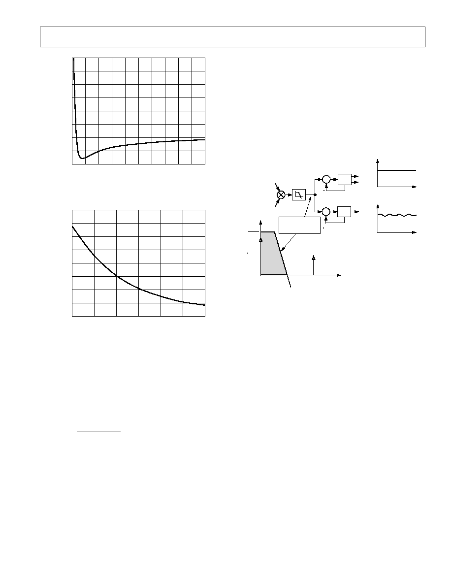
GENERAL DESCRIPTION
The ADE7755 is pin compatible with the AD7755. The only
difference between the ADE7755 and the AD7755 is that the
ADE7755 features a synchronous CF and F1/F2 outputs under
all load conditions.
The ADE7755 is a high accuracy electrical energy measurement
IC. The part specifications surpass the accuracy requirements as
quoted in the IEC1036 standard. See Analog Devices' Appli-
cation Note AN-559 for a description of an IEC1036 watt-hour
meter reference design based on the AD7755.
The only analog circuitry used in the ADE7755 is in the ADCs
and reference circuit. All other signal processing (e.g., multipli-
cation and filtering) is carried out in the digital domain. This
approach provides superior stability and accuracy over extremes
in environmental conditions and over time.
The ADE7755 supplies average real power information on the
low-frequency outputs F1 and F2. These logic outputs may be
used to directly drive an electromechanical counter or interface
to an MCU. The CF logic output gives instantaneous real power
information. This output is intended to be used for calibration
purposes or for interfacing to an MCU.
The ADE7755 includes a power supply monitoring circuit on the
AV
DD
supply pin. The ADE7755 will remain in a reset condition
until the supply voltage on AV
DD
reaches 4 V. If the supply falls
below 4 V, the ADE7755 will also be reset and no pulses will be
issued on F1, F2, and CF.
Internal phase matching circuitry ensures that the voltage and
current channels are phase matched whether the HPF in Chan-
nel 1 is on or off. An internal no-load threshold ensures that the
ADE7755 does not exhibit any creep when there is no load.
The ADE7755 is available in a 24-lead SSOP package.

REV. 0
2
ADE7755SPECIFICATIONS
(AV
DD
= DV
DD
= 5 V 5%, AGND = DGND = 0 V, On-Chip Reference,
CLKIN = 3.58 MHz, T
MIN
to T
MAX
= 40 C to +85 C.)
Parameter
Specifications
Unit
Test Conditions/Comments
ACCURACY
1, 2
Measurement Error
1
on Channel 1
Channel 2 with Full-Scale Signal (
±660 mV), 25C
Gain = 1
0.1
% Reading typ
Over a Dynamic Range 500 to 1
Gain = 2
0.1
% Reading typ
Over a Dynamic Range 500 to 1
Gain = 8
0.1
% Reading typ
Over a Dynamic Range 500 to 1
Gain = 16
0.1
% Reading typ
Over a Dynamic Range 500 to 1
Phase Error
1
Between Channels
Line Frequency = 45 Hz to 65 Hz
V1 Phase Lead 37
(PF = 0.8 Capacitive)
±0.1
Degrees(
) max AC/DC = 0 and AC/DC = 1
V1 Phase Lag 60
(PF = 0.5 Inductive)
±0.1
Degrees(
) max AC/DC = 0 and AC/DC = 1
AC Power Supply Rejection
1
AC/
DC = 1, S0 = S1 = 1, G0 = G1 = 0
Output Frequency Variation (CF)
0.2
% Reading typ
V1 = 100 mV rms, V2 = 100 mV rms, @ 50 Hz
Ripple on AV
DD
of 200 mV rms @ 100 Hz
DC Power Supply Rejection
1
AC/
DC = 1, S0 = S1 = 1, G0 = G1 = 0
Output Frequency Variation (CF)
±0.3
% Reading typ
V1 = 100 mV rms, V2 = 100 mV rms,
AV
DD
= DV
DD
= 5 V
± 250 mV
ANALOG INPUTS
See Analog Inputs section
Maximum Signal Levels
±1
V max
V1P, V1N, V2N, and V2P to AGND
Input Impedance (DC)
390
k
W min
CLKIN = 3.58 MHz
Bandwidth (3 dB)
14
kHz typ
CLKIN/256, CLKIN = 3.58 MHz
ADC Offset Error
1, 2
±25
mV max
Gain = 1, See Terminology and Performance Graphs
Gain Error
1
±7
% Ideal typ
External 2.5 V Reference, Gain = 1
V1 = 470 mV dc, V2 = 660 mV dc
Gain Error Match
1
±0.2
% Ideal typ
External 2.5 V Reference
REFERENCE INPUT
REF
IN/OUT
Input Voltage Range
2.7
V max
2.5 V + 8%
2.3
V min
2.5 V 8%
Input Impedance
3.2
k
W min
Input Capacitance
10
pF max
ON-CHIP REFERENCE
Nominal 2.5 V
Reference Error
±200
mV max
Temperature Coefficient
±30
ppm/
C typ
CLKIN
Note All Specifications for CLKIN of 3.58 MHz
Input Clock Frequency
4
MHz max
1
MHz min
LOGIC INPUTS
3
SCF, S0, S1, AC/
DC,
RESET, G0, and G1
Input High Voltage, V
INH
2.4
V min
DV
DD
= 5 V
± 5%
Input Low Voltage, V
INL
0.8
V max
DV
DD
= 5 V
± 5%
Input Current, I
IN
±3
mA max
Typically 10 nA, V
IN
= 0 V to DV
DD
Input Capacitance, C
IN
10
pF max
LOGIC OUTPUTS
3
F1 and F2
Output High Voltage, V
OH
I
SOURCE
= 10 mA
4.5
V min
DV
DD
= 5 V
Output Low Voltage, V
OL
I
SINK
= 10 mA
0.5
V max
DV
DD
= 5 V
CF and REVP
Output High Voltage, V
OH
I
SOURCE
= 5 mA
4
V min
DV
DD
= 5 V
Output Low Voltage, V
OL
I
SINK
= 5 mA
0.5
V max
DV
DD
= 5 V

REV. 0
3
ADE7755
Parameter
Specifications
Unit
Test Conditions/Comments
POWER SUPPLY
For Specified Performance
AV
DD
4.75
V min
5 V 5%
5.25
V max
5 V + 5%
DV
DD
4.75
V min
5 V 5%
5.25
V max
5 V + 5%
AI
DD
3
mA max
Typically 2 mA
DI
DD
2.5
mA max
Typically 1.5 mA
NOTES
1
See Terminology section for explanation of specifications.
2
See Plots in Typical Performance Graphs.
3
Sample tested during initial release and after any redesign or process change that may affect this parameter.
Specifications subject to change without notice.
TIMING CHARACTERISTICS
1, 2
Parameter
Specifications
Unit
Test Conditions/Comments
t
1
3
275
ms
F1 and F2 Pulsewidth (Logic Low)
t
2
See Table III
sec
Output Pulse Period. See Transfer Function section.
t
3
1/2 t
2
sec
Time between F1 Falling Edge and F2 Falling Edge
t
4
3, 4
90
ms
CF Pulsewidth (Logic High)
t
5
See Table IV
sec
CF Pulse Period. See Transfer Function section.
t
6
CLKIN/4
sec
Minimum Time between F1 and F2 Pulse
NOTES
1
Sample tested during initial release and after any redesign or process change that may affect this parameter.
2
See Figure 1.
3
The pulsewidths of F1, F2, and CF are not fixed for higher output frequencies. See Frequency Outputs section.
4
The CF pulse is always 18
ms in the high-frequency mode. See Frequency Outputs section and Table IV.
Specifications subject to change without notice.
(AV
DD
= DV
DD
= 5 V 5%, AGND = DGND = 0 V, On-Chip Reference, CLKIN = 3.58 MHz, T
MIN
to
T
MAX
= 40 C to +85 C.)
CAUTION
ESD (electrostatic discharge) sensitive device. Electrostatic charges as high as 4000 V readily
accumulate on the human body and test equipment and can discharge without detection. Although
the ADE7755 features proprietary ESD protection circuitry, permanent damage may occur on
devices subjected to high-energy electrostatic discharges. Therefore, proper ESD precautions are
recommended to avoid performance degradation or loss of functionality.
WARNING!
ESD SENSITIVE DEVICE
ABSOLUTE MAXIMUM RATINGS
*
(T
A
= 25
C unless otherwise noted.)
AV
DD
to AGND . . . . . . . . . . . . . . . . . . . . . . . 0.3 V to +7 V
DV
DD
to DGND . . . . . . . . . . . . . . . . . . . . . . . 0.3 V to +7 V
DV
DD
to AV
DD
. . . . . . . . . . . . . . . . . . . . . . 0.3 V to +0.3 V
Analog Input Voltage to AGND
V1P, V1N, V2P, and V2N . . . . . . . . . . . . . . . 6 V to +6 V
Reference Input Voltage to AGND . . 0.3 V to AV
DD
+ 0.3 V
Digital Input Voltage to DGND . . . 0.3 V to DV
DD
+ 0.3 V
Digital Output Voltage to DGND . . 0.3 V to DV
DD
+ 0.3 V
Operating Temperature Range
Industrial . . . . . . . . . . . . . . . . . . . . . . . . . . 40
C to +85C
Storage Temperature Range . . . . . . . . . . . . 65
C to +150C
Junction Temperature . . . . . . . . . . . . . . . . . . . . . . . . . 150
C
24-Lead SSOP, Power Dissipation . . . . . . . . . . . . . . 450 mW
q
JA
Thermal Impedance . . . . . . . . . . . . . . . . . . . . 112
C/W
Lead Temperature, Soldering
Vapor Phase (60 sec) . . . . . . . . . . . . . . . . . . . . . . 215
C
Infrared (15 sec) . . . . . . . . . . . . . . . . . . . . . . . . . . . 220
C
*Stresses above those listed under Absolute Maximum Ratings may cause perma-
nent damage to the device. This is a stress rating only; functional operation of the
device at these or any other conditions above those listed in the operational
sections of this specification is not implied. Exposure to absolute maximum rating
conditions for extended periods may affect device reliability.
ORDERING GUIDE
Model
Package Description
Package Options
ADE7755ARS
Shrink Small Outline Package
RS-24
ADE7755ARSRL
Shrink Small Outline Package in Reel
RSRL-24
ADE7755AN-REF
ADE7755 Reference Design PCB (See AN-559)
EVAL-ADE7755EB
ADE7755 Evaluation Board
REV. 0
ADE7755
4
.
t
2
.
t
3
t
4
.
t
5
.
t
6
t
1
F1
F2
CF
Figure 1. Timing Diagram for Frequency Outputs
PIN CONFIGURATION
TOP VIEW
(Not to Scale)
24
23
22
21
20
19
18
17
16
15
14
13
1
2
3
4
5
6
7
8
9
10
11
12
ADE7755
NC = NO CONNECT
DV
DD
AC/DC
AV
DD
NC
F1
V1P
V1N
V2N
V2P
RESET
REF
IN/OUT
AGND
SCF
F2
CF
DGND
REVP
NC
CLKOUT
CLKIN
G0
G1
S0
S1

REV. 0
ADE7755
5
PIN FUNCTION DESCRIPTIONS
Pin No.
Mnemonic
Description
1
DV
DD
Digital Power Supply. This pin provides the supply voltage for the digital circuitry in the ADE7755.
The supply voltage should be maintained at 5 V
± 5% for specified operation. This pin should be
decoupled with a 10
mF capacitor in parallel with a ceramic 100 nF capacitor.
2
AC/
DC
High-Pass Filter Select. This logic input is used to enable the HPF in Channel 1 (Current Channel).
A logic one on this pin enables the HPF. The associated phase response of this filter has been inter-
nally compensated over a frequency range of 45 Hz to 1 kHz. The HPF filter should be enabled in
power metering applications.
3
AV
DD
Analog Power Supply. This pin provides the supply voltage for the analog circuitry in the ADE7755.
The supply should be maintained at 5 V
± 5% for specified operation. Every effort should be made to
minimize power supply ripple and noise at this pin by the use of proper decoupling. This pin should
be decoupled to AGND with a 10
mF capacitor in parallel with a ceramic 100 nF capacitor.
4, 19
NC
No Connect
5, 6
V1P, V1N
Analog Inputs for Channel 1 (Current Channel). These inputs are fully differential voltage inputs with
a maximum differential signal level of
±470 mV for specified operation. Channel 1 also has a PGA,
and the gain selections are outlined in Table I. The maximum signal level at these pins is
±1 V with
respect to AGND. Both inputs have internal ESD protection circuitry. An overvoltage of
±6 V can be
sustained on these inputs without risk of permanent damage.
7, 8
V2N, V2P
Negative and Positive Inputs for Channel 2 (Voltage Channel). These inputs provide a fully differential
input pair. The maximum differential input voltage is
±660 mV for specified operation. The maxi-
mum signal level at these pins is
±1 V with respect to AGND. Both inputs have internal ESD
protection circuitry, and an overvoltage of
±6 V can also be sustained on these inputs without risk of
permanent damage.
9
RESET
Reset Pin for the ADE7755. A logic low on this pin will hold the ADCs and digital circuitry in a reset
condition. Bringing this pin logic low will clear the ADE7755 internal registers.
10
REF
IN/OUT
This pin provides access to the on-chip voltage reference. The on-chip reference has a nominal value
of 2.5 V
± 8% and a typical temperature coefficient of 30 ppm/C. An external reference source may
also be connected at this pin. In either case, this pin should be decoupled to AGND with a 1
mF
ceramic capacitor and 100 nF ceramic capacitor.
11
AGND
This provides the ground reference for the analog circuitry in the ADE7755, i.e., ADCs and reference.
This pin should be tied to the analog ground plane of the PCB. The analog ground plane is the ground
reference for all analog circuitry, e.g., antialiasing filters and current and voltage transducers. For good
noise suppression, the analog ground plane should only connect to the digital ground plane at one
point. A star ground configuration will help to keep noisy digital currents away from the analog circuits.
12
SCF
Select Calibration Frequency. This logic input is used to select the frequency on the calibration output
CF. Table IV shows how the calibration frequencies are selected.
13, 14
S1, S0
These logic inputs are used to select one of four possible frequencies for the digital-to-frequency
conversion. This offers the designer greater flexibility when designing the energy meter. See Selecting
a Frequency for an Energy Meter Application section.
15, 16
G1, G0
These logic inputs are used to select one of four possible gains for Channel 1, i.e., V1. The possible
gains are 1, 2, 8, and 16. See Analog Input section.
17
CLKIN
An external clock can be provided at this logic input. Alternatively, a parallel resonant AT crystal can
be connected across CLKIN and CLKOUT to provide a clock source for the ADE7755. The clock
frequency for specified operation is 3.579545 MHz. Crystal load capacitance of between 22 pF and
33 pF (ceramic) should be used with the gate oscillator circuit.
18
CLKOUT
A crystal can be connected across this pin and CLKIN as described above to provide a clock source
for the ADE7755. The CLKOUT Pin can drive one CMOS load when an external clock is supplied at
CLKIN or by the gate oscillator circuit.
20
REVP
This logic output will go logic high when negative power is detected, i.e., when the phase angle between
the voltage and current signals is greater than 90
. This output is not latched and will be reset when
positive power is once again detected. The output will go high or low at the same time as a pulse is
issued on CF.

REV. 0
ADE7755
6
Pin No.
Mnemonic
Description
21
DGND
This provides the ground reference for the digital circuitry in the ADE7755, i.e., multiplier, filters, and
digital-to-frequency converter. This pin should be tied to the digital ground plane of the PCB. The
digital ground plane is the ground reference for all digital circuitry, e.g., counters (mechanical and
digital), MCUs, and indicator LEDs. For good noise suppression, the analog ground plane should
only be connected to the digital ground plane at one point only, e.g., a star ground.
22
CF
Calibration Frequency Logic Output. The CF logic output gives instantaneous real power informa-
tion. This output is intended to be used for calibration purposes. Also see SCF Pin description.
23, 24
F2, F1
Low Frequency Logic Outputs. F1 and F2 supply average real power information. The logic outputs
can be used to directly drive electromechanical counters and two phase stepper motors. See Transfer
Function section.
TERMINOLOGY
MEASUREMENT ERROR
The error associated with the energy measurement made by the
ADE7755 is defined by the following formula:
Percentage Error
True Energy
=
¥
Energy Registered by the ADE7755 True Energy
100%
PHASE ERROR BETWEEN CHANNELS
The HPF (High-Pass Filter) in Channel 1 has a phase lead
response. To offset this phase response and equalize the phase
response between channels, a phase correction network is also
placed in Channel 1. The phase correction network matches the
phase to within
±0.1 over a range of 45 Hz to 65 Hz and ±0.2
over a range 40 Hz to 1 kHz. See Figures 4 and 5.
POWER SUPPLY REJECTION
This quantifies the ADE7755 measurement error as a percent-
age of the reading when the power supplies are varied.
For the ac PSR measurement, a reading at nominal supplies
(5 V) is taken. A 200 mV rms/100 Hz signal is then introduced
onto the supplies and a second reading obtained under the same
input signal levels. Any error introduced is expressed as a
percentage of the reading (see Measurement Error definition).
For the dc PSR measurement, a reading at nominal supplies
(5 V) is taken. The supplies are then varied
±5% and a second
reading is obtained with the same input signal levels. Any error
introduced is again expressed as a percentage of the reading.
ADC OFFSET ERROR
This refers to the dc offset associated with the analog inputs to
the ADCs. It means that with the analog inputs connected to
AGND, the ADCs still see a small dc signal (offset). The offset
decreases with increasing gain in Channel V1. This specification
is measured at a gain of 1. At a gain of 16, the dc offset is typi-
cally less than 1 mV. However, when the HPF is switched on,
the offset is removed from the current channel and the power
calculation is not affected by this offset.
GAIN ERROR
The gain error of the ADE7755 is defined as the difference between
the measured output frequency (minus the offset) and the ideal
output frequency. It is measured with a gain of 1 in Channel V1.
The difference is expressed as a percentage of the ideal frequency.
The ideal frequency is obtained from the ADE7755 transfer
function (see Transfer Function section).
GAIN ERROR MATCH
The gain error match is defined as the gain error (minus the off-
set) obtained when switching between a gain of 1 and a gain of 2,
8, or 16. It is expressed as a percentage of the output frequency
obtained under a gain of 1. This gives the gain error observed
when the gain selection is changed from 1 to 2, 8, or 16.
REV. 0
ADE7755
7
Amps
0.5
0.01
0.1
% ERROR
0.4
0.3
0.2
0.1
0.0
0.1
0.2
0.3
0.4
0.5
1
10
100
+25 C
+85 C
40 C
PF = 1
GAIN = 1
ON-CHIP REFERENCE
TPC 1. Error as a % of Reading (Gain = 1)
Amps
0.5
0.01
0.1
% ERROR
0.4
0.3
0.2
0.1
0.0
0.1
0.2
0.3
0.4
0.5
1
10
100
+25 C
+85 C
40 C
PF = 1
GAIN = 2
ON-CHIP REFERENCE
TPC 2. Error as a % of Reading (Gain = 2)
Amps
0.4
0.01
0.1
% ERROR
0.3
0.2
0.1
0.0
0.1
0.2
0.3
0.4
0.5
0.6
1
10
100
+25 C
+85 C
40 C
PF = 1
GAIN = 8
ON-CHIP REFERENCE
TPC 3. Error as a % of Reading (Gain = 8)
Typical Performance Characteristics
Amps
0.5
0.01
0.1
% ERROR
0.4
0.3
0.2
0.1
0.0
0.1
0.2
0.3
0.4
0.5
1
10
100
+25 C
+85 C
40 C
PF = 1
GAIN = 16
ON-CHIP REFERENCE
TPC 4. Error as a % of Reading (Gain = 16)
Amps
0.6
0.01
0.1
% ERROR
0.4
0.2
0.0
0.2
0.4
0.6
1
10
100
40 C PF = 0.5
+25 C PF = 1
+25 C PF = 0.5
+85 C PF = 0.5
PF = 0.5
GAIN = 1
ON-CHIP REFERENCE
TPC 5. Error as a % of Reading (Gain = 1)
Amps
0.6
0.01
0.1
% ERROR
0.4
0.2
0.0
0.2
0.4
0.6
1
10
100
40 C PF = 0.5
+25 C PF = 1
+25 C PF = 0.5
+85 C PF = 0.5
PF = 0.5
GAIN = 2
ON-CHIP REFERENCE
TPC 6. Error as a % of Reading (Gain = 2)
REV. 0
ADE7755
8
Amps
0.01
0.1
% ERROR
0.0
1
10
100
40 C PF = 0.5
+25 C PF = 1
+25 C PF = 0.5
+85 C PF = 0.5
0.2
0.4
0.6
0.8
0.8
0.6
0.4
0.2
PF = 0.5
GAIN = 8
ON-CHIP REFERENCE
TPC 7. Error as a % of Reading (Gain = 8)
Amps
0.01
0.1
% ERROR
0.8
0.6
0.2
0.4
0.0
0.2
0.4
1
10
100
40 C PF = 0.5
1.0
+25 C PF = 1
+25 C PF = 0.5
+85 C PF = 0.5
PF = 0.5
GAIN = 16
ON-CHIP REFERENCE
TPC 8. Error as a % of Reading (Gain = 16)
Amps
0.4
0.01
0.1
% ERROR
0.2
0.1
0.0
1
10
100
40 C
PF = 1
GAIN = 2
EXTERNAL REFERENCE
+25 C
+85 C
0.3
0.4
0.2
0.1
0.3
TPC 9. Error as a % of Reading over Temperature
with an External Reference (Gain = 2)
Amps
0.01
0.1
% ERROR
0.4
0.3
0.2
0.1
0.0
0.1
0.2
0.3
0.4
1
10
100
+25 C
+85 C
40 C
PF = 1
GAIN = 16
EXTERNAL REFERENCE
TPC 10. Error as a % of Reading over Temperature
with an External Reference (Gain = 16)
FREQUENCY Hz
% ERROR
0.8
0.6
0.4
0.2
0.0
0.2
0.4
0.6
45
50
55
60
65
70
75
PF = 1
PF = 0.5
TPC 11. Error as a % of Reading over Frequency
33nF
1k
AV
DD
AC/DC DV
DD
33nF
1k
1M
220V
NC
V1P
V1N
REF
IN/OUT
33nF
1k
100nF
33nF
1k
V2N
V2P
100nF
10 F
10 F
100nF
10 F
V
DD
RESET AGND DGND
F1
F2
CF
REVP
NC
CLKOUT
CLKIN
G0
G1
S0
S1
SCF
Y1
3.58MHz
10nF
10nF
10nF
33pF
33pF
500
1.5m
10m
40A TO
40mA
GAIN
SELECT
U3
PS2501-1
K7
K8
U1
ADE7755
10k
V
DD
V
DD
NC = NO CONNECT
TPC 12. Test Circuit for Performance Curves
REV. 0
ADE7755
9
FREQUENCY Hz
15
PHASE Degrees
2
0
4
6
8
10
12
14
16
9
3
3
9
15
GAIN = 1
TEMPERATURE = 25 C
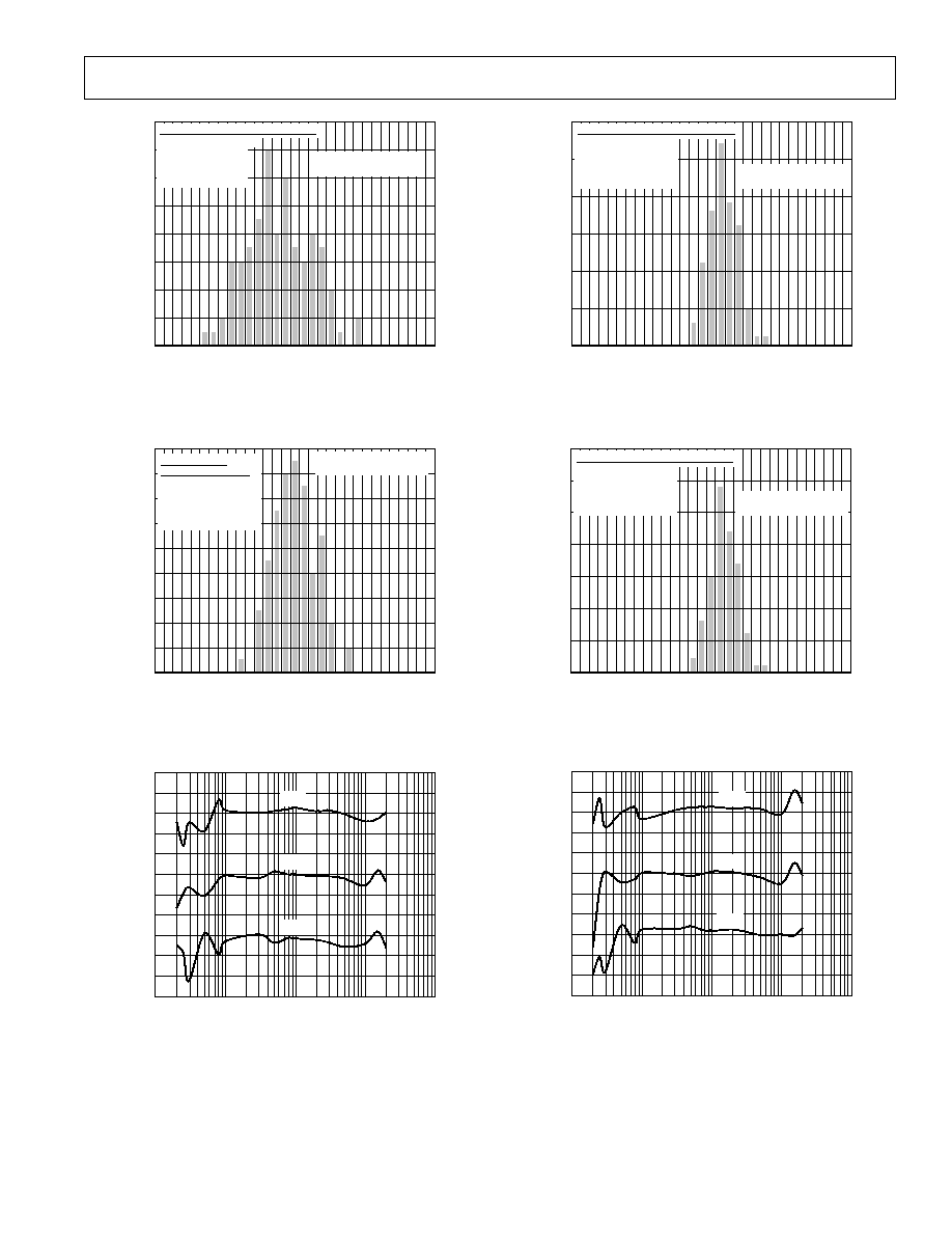
DISTRIBUTION CHARACTERISTICS
NUMBER POINTS: 101
MINIMUM: 9.78871
MAXIMUM: 7.2939
MEAN: 1.73203
STD. DEV: 3.61157
TPC 13. Channel 1 Offset Distribution (Gain = 1)
FREQUENCY Hz
15
PHASE Degrees
2
0
4
6
8
12
14
16
18
9
3
3
9
15
GAIN = 2
TEMPERATURE = 25 C
DISTRIBUTION
CHARACTERISTICS
NUMBER POINTS: 101
MINIMUM: 5.61779
MAXIMUM: 6.40821
MEAN: 0.01746
STD. DEV: 2.35129
10
TPC 14. Channel 1 Offset Distribution (Gain = 2)
Amps
0.01
100
0.1
% ERROR
1
10
0.4
0.3
0.6
0.2
0.1
0
0.1
0.2
0.3
0.4
0.5
5V
4.75V
5.25V
0.5
TPC 15. PSR with Internal Reference (Gain = 16)
FREQUENCY Hz
15
PHASE Degrees
5
0
10
15
20
25
30
9
3
3
9
15
GAIN = 8
TEMPERATURE = 25 C
DISTRIBUTION CHARACTERISTICS
NUMBER POINTS: 101
MINIMUM: 2.48959
MAXIMUM: 5.81126
MEAN: 1.26847
STD. DEV: 1.57404
TPC 16. Channel 1 Offset Distribution (Gain = 8)
FREQUENCY Hz
15
PHASE Degrees
10
0
15
20
25
30
35
9
3
3
9
15
GAIN = 16
TEMPERATURE = 25 C
DISTRIBUTION CHARACTERISTICS
NUMBER POINTS: 101
MINIMUM: 1.96823
MAXIMUM: 5.71177
MEAN: 1.48279
STD. DEV: 1.47802
5
TPC 17. Channel 1 Offset Distribution (Gain = 16)
Amps
0.01
100
0.1
% ERROR
1
10
0.4
0.3
0.6
0.2
0.1
0
0.1
0.2
0.3
0.4
0.5
0.5
4.75V
5.25V
5V
TPC 18. PSR with External Reference (Gain = 16)
REV. 0
ADE7755
10
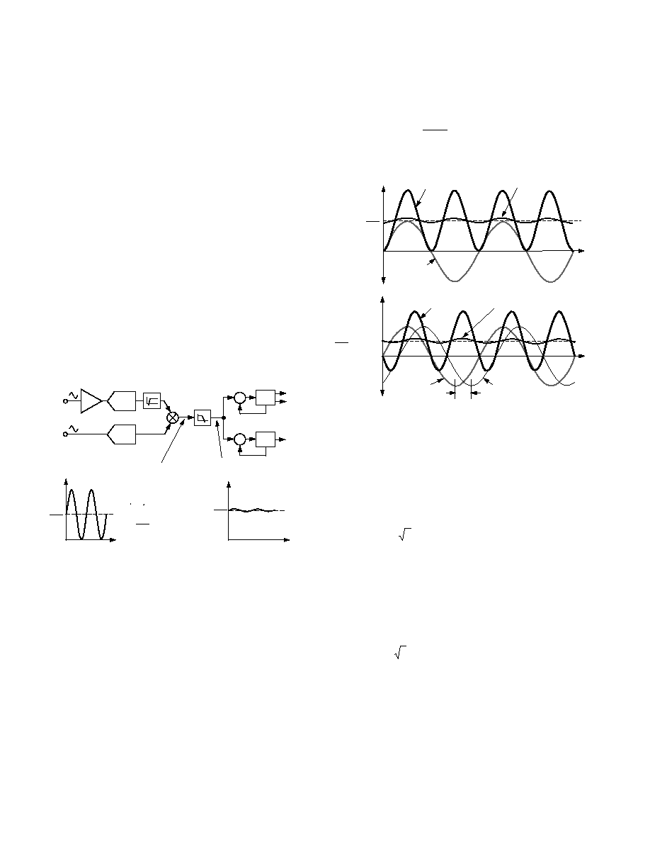
THEORY OF OPERATION
The two ADCs digitize the voltage signals from the current and
voltage transducers. These ADCs are 16-bit second order
sigma-delta with an oversampling rate of 900 kHz. This analog
input structure greatly simplifies transducer interfacing by
providing a wide dynamic range for direct connection to the
transducer and also by simplifying the antialiasing filter design.
A programmable gain stage in the current channel further facili-
tates easy transducer interfacing. A high-pass filter in the current
channel removes any dc component from the current signal.
This eliminates any inaccuracies in the real power calculation
due to offsets in the voltage or current signals (see HPF and
Offset Effects section).
The real power calculation is derived from the instantaneous
power signal. The instantaneous power signal is generated by a
direct multiplication of the current and voltage signals. In order
to extract the real power component (i.e., the dc component),
the instantaneous power signal is low-pass filtered. Figure 2
illustrates the instantaneous real power signal and shows how the
real power information can be extracted by low-pass filtering the
instantaneous power signal. This scheme correctly calculates real
power for nonsinusoidal current and voltage waveforms at all
power factors. All signal processing is carried out in the digital
domain for superior stability over temperature and time.
LPF
DIGITAL-TO-
FREQUENCY
F1
F2
CH1
INSTANTANEOUS REAL
POWER SIGNAL
MULTIPLIER
PGA
CH2
ADC
INSTANTANEOUS
POWER SIGNAL p(t)
V
I
2
V I
V I
2
p(t) = i(t) v(t)
WHERE:
v(t) = V cos( t)
i(t) = I cos( t)
p(t) =
V I
2
{
1+cos (2 t)}
ADC
TIME
HPF
DIGITAL-TO-
FREQUENCY
CF
Figure 2. Signal Processing Block Diagram
The low-frequency output of the ADE7755 is generated by
accumulating this real power information. This low frequency
inherently means a long accumulation time between output
pulses. The output frequency is therefore proportional to the
average real power. This average real power information can, in
turn, be accumulated (e.g., by a counter) to generate real energy
information. Because of its high output frequency and shorter
integration time, the CF output is proportional to the instanta-
neous real power. This is useful for system calibration purposes
that would take place under steady load conditions.
Power Factor Considerations
The method used to extract the real power information from the
instantaneous power signal (i.e., by low-pass filtering) is still
valid even when the voltage and current signals are not in phase.
Figure 3 displays the unity power factor condition and a DPF
(Displacement Power Factor) = 0.5, i.e., current signal lagging
the voltage by 60
. If we assume the voltage and current wave-
forms are sinusoidal, the real power component of the instanta-
neous power signal (i.e., the dc term) is given by:
V
I
¥
Ê
Ë
Á
^
¯
~ ¥
( )
2
60
cos
o
This is the correct real power calculation.
INSTANTANEOUS
REAL POWER SIGNAL
INSTANTANEOUS
POWER SIGNAL
V I
2
cos(60 )
V I
2
INSTANTANEOUS
POWER SIGNAL
INSTANTANEOUS
REAL POWER SIGNAL
60
CURRENT
CURRENT
VOLTAGE
0V
0V
VOLTAGE
Figure 3. DC Component of Instantaneous Power Signal
Conveys Real Power Information PF < 1
Nonsinusoidal Voltage and Current
The real power calculation method also holds true for nonsinu-
soidal current and voltage waveforms. All voltage and current
waveforms in practical applications will have some harmonic
content. Using the Fourier Transform, instantaneous voltage
and current waveforms can be expressed in terms of their
harmonic content.
v t
V
Vh
h t
h
O
h
( )
sin(
)
=
+
¥
¥
+
·
Â
2
0
w
a
(1)
where:
v(t)
is the instantaneous voltage
V
O
is the average value
Vh
is the rms value of voltage harmonic h
and
h
is the phase angle of the voltage harmonic
i t
I
Ih
h t
h
O
h
( )
sin(
)
=
+
¥
¥
+
·
Â
2
0
w b
(2)
where:
i(t)
is the instantaneous current
I
O
is the dc component
Ih
is the rms value of current harmonic h
and
h
is the phase angle of the current harmonic
REV. 0
ADE7755
11
Using Equations 1 and 2, the real power P can be expressed in
terms of its fundamental real power (P
1
) and harmonic real
power (P
H
).
P
P
P
H
=
+
1
where:
P
V
I
1
1
1
1
1
1
1
=
¥
=
cos
f
f
a
b
(3)
and:
P
Vh
Ih
h
h
h
h
H
h
= Â
¥
=
·
1
cos
f
f
a b
(4)
As can be seen from Equation 4 above, a harmonic real power
component is generated for every harmonic, provided that har-
monic is present in both the voltage and current waveforms.
The power factor calculation has previously been shown to be
accurate in the case of a pure sinusoid; therefore the harmonic
real power must also correctly account for the power factor
since it is made up of a series of pure sinusoids.
Note that the input bandwidth of the analog inputs is 14 kHz
with a master clock frequency of 3.5795 MHz.
ANALOG INPUTS
Channel V1 (Current Channel )
The voltage output from the current transducer is connected to
the ADE7755 here. Channel V1 is a fully differential voltage
input. V1P is the positive input with respect to V1N.
The maximum peak differential signal on Channel 1 should be
less than
±470 mV (330 mV rms for a pure sinusoidal signal) for
specified operation. Note that Channel 1 has a programmable
gain amplifier (PGA) with user selectable gain of 1, 2, 8, or 16
(see Table I). These gains facilitate easy transducer interfacing.
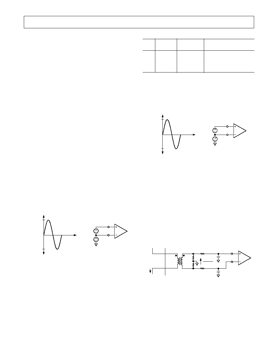
DIFFERENTIAL INPUT
470mV MAX PEAK
+470mV
AGND
V
CM
V1
V1P
V
CM
470mV
COMMON-MODE
100mV MAX
V1N
V1
Figure 4. Maximum Signal Levels, Channel 1, Gain = 1
The diagram in Figure 4 illustrates the maximum signal levels
on V1P and V1N. The maximum differential voltage is
±470 mV
divided by the gain selection. The differential voltage signal on
the inputs must be referenced to a common mode, e.g., AGND.
The maximum common-mode signal is
±100 mV as shown in
Figure 4.
Table I. Gain Selection for Channel 1
Maximum
G1
G0
Gain
Differential Signal
0
0
1
±470 mV
0
1
2
±235 mV
1
0
8
±60 mV
1
1
16
±30 mV
Channel V2 (Voltage Channel )
The output of the line voltage transducer is connected to the
ADE7755 at this analog input. Channel V2 is a fully differential
voltage input. The maximum peak differential signal on
Channel 2 is
±660 mV. Figure 5 illustrates the maximum
signal levels that can be connected to the ADE7755 Channel 2.
DIFFERENTIAL INPUT
660mV MAX PEAK
+660mV
AGND
V
CM
V2
V2P
V
CM
660mV
COMMON-MODE
100mV MAX
V2N
V2
Figure 5. Maximum Signal Levels, Channel 2
Channel 2 must be driven from a common-mode voltage, i.e.,
the differential voltage signal on the input must be referenced to
a common mode (usually AGND). The analog inputs of the
ADE7755 can be driven with common-mode voltages of up to
100 mV with respect to AGND. However, best results are
achieved using a common mode equal to AGND.
Typical Connection Diagrams
Figure 6 shows a typical connection diagram for Channel V1. A
CT (current transformer) is the current transducer selected for this
example. Notice the common-mode voltage for Channel 1 is
AGND and is derived by center tapping the burden resistor to
AGND. This provides the complementary analog input signals
for V1P and V1N. The CT turns ratio and burden resistor Rb
are selected to give a peak differential voltage of
±470 mV/Gain
at maximum load.
V1P
AGND
470mV
GAIN
Rb
Rf
Rf
CT
NEUTRAL
PHASE
IP
V1N
Cf
Cf
Figure 6. Typical Connection for Channel 1
REV. 0
ADE7755
12
Figure 7 shows two typical connections for Channel V2. The first
option uses a PT (potential transformer) to provide complete
isolation from the power line. In the second option, the
ADE7755 is biased around the neutral wire, and a resistor divider
provides a voltage signal that is proportional to the line voltage.
Adjusting the ratio of Ra, Rb, and VR is also a convenient way of
carrying out a gain calibration on the meter.
660mV
Ra
*
Rb
*
VR
*
V2P
AGND
Rf
Rf
CT
NEUTRAL
PHASE
V2N
Cf
Cf
660mV
V2P
Rf
NEUTRAL
PHASE
V2N
Cf
Cf
*
Ra >> Rb + VR
*
Rb + VR = Rf
Figure 7. Typical Connections for Channel 2
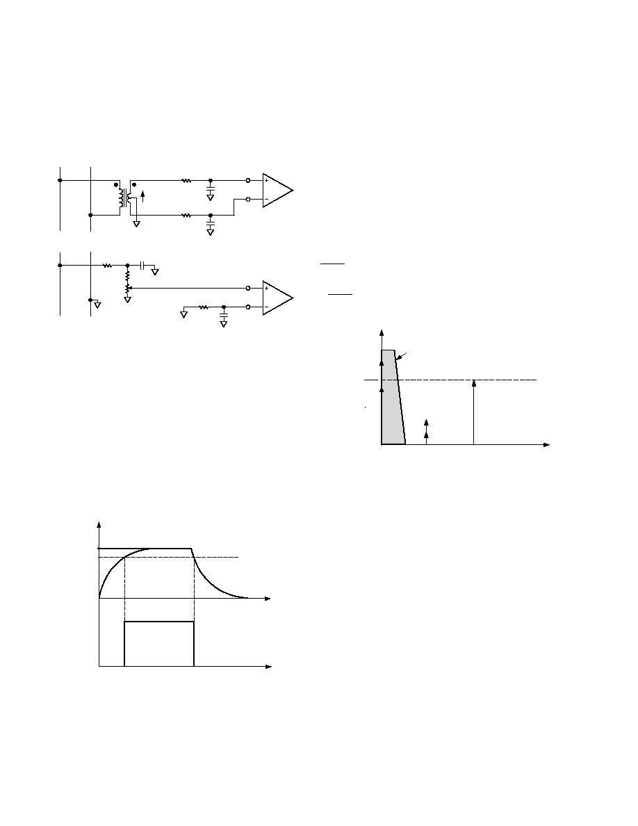
POWER SUPPLY MONITOR
The ADE7755 contains an on-chip power supply monitor. The
Analog Supply (AV
DD
) is continuously monitored by the ADE7755.
If the supply is less than 4 V
± 5%, the ADE7755 will be reset.
This is useful to ensure correct device startup at power-up and
power-down. The power supply monitor has built in hysteresis
and filtering. This gives a high degree of immunity to false trig-
gering due to noisy supplies.
In Figure 8, the trigger level is nominally set at 4 V. The toler-
ance on this trigger level is about
±5%. The power supply and
decoupling for the part should be such that the ripple at AV
DD
does not exceed 5 V
± 5% as specified for normal operation.
AV
DD
5V
4V
0V
INTERNAL
RESET
RESET
TIME
ACTIVE
RESET
Figure 8. On-Chip Power Supply Monitor
HPF and Offset Effects
Figure 9 shows the effect of offsets on the real power calculation.
An offset on Channel 1 and Channel 2 will contribute a dc
component after multiplication. Since the dc component is
extracted by the LPF, it will accumulate as real power. If not
properly filtered, dc offsets will introduce error to the energy
accumulation. This problem is easily avoided by enabling the
HPF (i.e., Pin AC/
DC is set logic high) in Channel 1. By
removing the offset from at least one channel, no error compo-
nent can be generated at dc by the multiplication. Error terms
at cos(
wt) are removed by the LPF and the digital-to-frequency
conversion (see Digital-to-Frequency Conversion section).
V
t
V
I
t
I
V
I
V
I
V
I
t
I
V
t
V
I
t
OS
OS
OS
OS
OS
OS
cos
cos
cos
cos
cos
w
w
w
w
w
( )
+
{
}
¥
( )
+
{
}
=
¥ +
¥
+
¥
( )
+
¥
( )
+ ¥ ¥
( )
2
2
2
V
OS
I
OS
I
OS
V
V
OS
I
DC COMPONENT (INCLUDING ERROR TERM)
IS EXTRACTED BY THE LPF FOR REAL
POWER CALCULATION
2
FREQUENCY RAD/S
2
V I
0
Figure 9. Effect of Channel Offset on the Real Power
Calculation
The HPF in Channel 1 has an associated phase response that is
compensated for on-chip. The phase compensation is activated
when the HPF is enabled and is disabled when the HPF is not
activated. Figures 10 and 11 show the phase error between chan-
nels with the compensation network activated. The ADE7755 is
phase compensated up to 1 kHz as shown. This will ensure correct
active harmonic power calculation even at low power factors.
REV. 0
ADE7755
13
FREQUENCY Hz
0
100
PHASE Degrees
0.05
0.10
0
0.05
0.10
0.15
0.20
0.25
0.30
200
300
400
500
600
700
800
900 1000
Figure 10. Phase Error between Channels (0 Hz to 1 kHz)
FREQUENCY Hz
40
PHASE Degrees
0.05
0.10
0
0.05
0.10
0.15
0.20
0.25
0.30
45
50
55
60
65
70
Figure 11. Phase Error between Channels (40 Hz to 70 Hz)
DIGITAL-TO-FREQUENCY CONVERSION
As previously described, the digital output of the low-pass filter
after multiplication contains the real power information. How-
ever, since this LPF is not an ideal "brick wall" filter implemen-
tation, the output signal also contains attenuated components
at the line frequency and its harmonics, i.e., cos(h
wt) where
h = 1, 2, 3, and so on.
The magnitude response of the filter is given by:
|
( )|
( / .
)
H f
f
Hz
=
+
1
1
8 9
(5)
For a line frequency of 50 Hz this would give an attenuation of
the 2
w (100 Hz) component of approximately 22 dBs. The
dominating harmonic will be at twice the line frequency, i.e.,
cos (2
wt), and this is due to the instantaneous power signal.
Figure 12 shows the instantaneous real power signal at the
output of the CPF, which still contains a significant amount of
instantaneous power information, i.e., cos (2
wt). This signal is
then passed to the digital-to-frequency converter where it is
integrated (accumulated) over time to produce an output frequency.
This accumulation of the signal will suppress or average out any
non-dc components in the instantaneous real power signal. The
average value of a sinusoidal signal is zero. Hence, the frequency
generated by the ADE7755 is proportional to the average real
power. Figure 12 shows the digital-to-frequency conversion for
steady load conditions, i.e., constant voltage and current.
2
V I
2
FREQUENCY RAD/S
LPF
DIGITAL-TO-
FREQUENCY
F1
F2
DIGITAL-TO-
FREQUENCY
CF
INSTANTANEOUS REAL POWER SIGNAL
(FREQUENCY DOMAIN)
MULTIPLIER
TIME
FREQUENCY
F1
FREQUENCY
FOUT
TIME
V
I
0
LPF TO EXTRACT
REAL POWER
(DC TERM)
cos(2 t)
ATTENUATED BY LPF
Figure 12. Real Power-to-Frequency Conversion
As can be seen in the diagram, the frequency output CF is seen
to vary over time, even under steady load conditions. This
frequency variation is primarily due to the cos (2
wt) component
in the instantaneous real power signal. The output frequency on
CF can be up to 2048 times higher than the frequency on F1
and F2. This higher output frequency is generated by accumu-
lating the instantaneous real power signal over a much shorter
time while converting it to a frequency. This shorter accumula-
tion period means less averaging of the cos (2
wt) component.
As a consequence, some of this instantaneous power signal passes
through the digital-to-frequency conversion. This will not be a
problem in the application. When CF is used for calibration
purposes, the frequency should be averaged by the frequency
counter. This will remove any ripple. If CF is measuring energy,
e.g., in a microprocessor-based application, the CF output
should also be averaged to calculate power. Because the outputs
F1 and F2 operate at a much lower frequency, more averaging
of the instantaneous real power signal is carried out. The result
is a greatly attenuated sinusoidal content and a virtually ripple-
free frequency output.
REV. 0
ADE7755
14
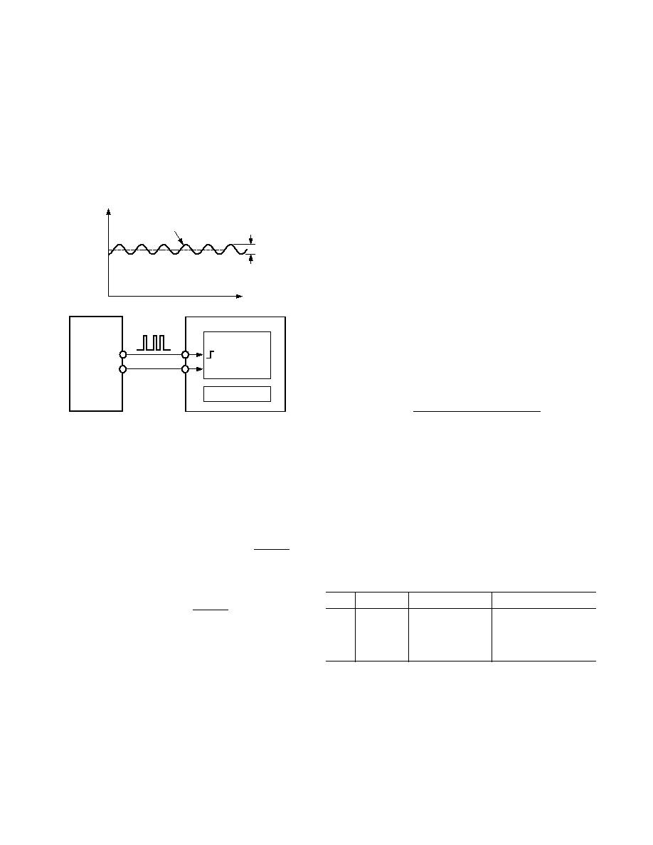
Interfacing the ADE7755 to a Microcontroller for Energy
Measurement
The easiest way to interface the ADE7755 to a microcontroller
is to use the CF high-frequency output with the output frequency
scaling set to 2048
¥ F1, F2. This is done by setting SCF = 0
and S0 = S1 = 1 (see Table IV). With full-scale ac signals on the
analog inputs, the output frequency on CF will be approximately
5.5 kHz. Figure 13 illustrates one scheme that could be used to
digitize the output frequency and carry out the necessary
averaging mentioned in the previous section.
TIME
10%
AVERAGE
FREQUENCY
CF
FREQUENCY
RIPPLE
MCU
UP/DOWN
COUNTER
TIMER
CF
REVP
*
ADE7755
*
REVP MUST BE USED IF THE METER IS BIDIRECTIONAL OR
DIRECTION OF ENERGY FLOW IS NEEDED
Figure 13. Interfacing the ADE7755 to an MCU
As shown, the frequency output CF is connected to an MCU
counter or port. This will count the number of pulses in a given
integration time that is determined by an MCU internal timer.
The average power proportional to the average frequency is
given by:
Average Frequency
Average
al Power
Counter
Timer
=
=
Re
The energy consumed during an integration period is given by:
Energy
Average Power
Time
Counter
Time
Time
Counter
=
¥
=
¥
=
For the purpose of calibration, this integration time can be 10 to
20 seconds to accumulate enough pulses to ensure correct aver-
aging of the frequency. In normal operation, the integration time
can be reduced to one or two seconds depending, for example,
on the required undate rate of a display. With shorter integra-
tion times on the MCU, the amount of energy in each update
may still have some small amount of ripple, even under steady
load conditions. However, over a minute or more, the measured
energy will have no ripple.
Power Measurement Considerations
Calculating and displaying power information will always have
some associated ripple that will depend on the integration period
used in the MCU to determine average power and also the load.
For example, at light loads, the output frequency may be 10 Hz.
With an integration period of two seconds, only about 20 pulses
will be counted. The possibility of missing one pulse always exists,
since the ADE7755 output frequency is running asynchronously
to the MCU timer. This would result in a one-in-twenty (or
5%) error in the power measurement.
TRANSFER FUNCTION
Frequency Outputs F1 and F2
The ADE7755 calculates the product of two voltage signals (on
Channel 1 and Channel 2) and then low-pass filters this product
to extract real power information. This real power information
is then converted to a frequency. The frequency information is
output on F1 and F2 in the form of active low pulses. The pulse
rate at these outputs is relatively low, e.g., 0.34 Hz maximum
for ac signals with S0 = S1 = 0 (see Table III). This means that
the frequency at these outputs is generated from real power
information accumulated over a relatively long period of time.
The result is an output frequency that is proportional to the
average real power. The averaging of the real power signal is
implicit to the digital-to-frequency conversion. The output
frequency or pulse rate is related to the input voltage signals by
the following equation.
Freq
V
V
Gain
F
V
REF
=
¥
¥
¥
¥
-
8 06
1
2
1 4
2
.
where:
Freq = Output frequency on F1 and F2 (Hz)
V1 = Differential rms voltage signal on Channel 1 (Volts)
V2 = Differential rms voltage signal on Channel 2 (Volts)
Gain = 1, 2, 8, or 16, depending on the PGA gain selection
made using logic inputs G0 and G1
V
REF
= The reference voltage (2.5 V
± 8%) (Volts)
F
14
= One of four possible frequencies selected by using the
logic inputs S0 and S1--see Table II
Table II. F
14
Frequency Selection
S1
S0
F
14
(Hz)
XTAL/CLKIN
*
0
0
1.7
3.579 MHz/2
21
0
1
3.4
3.579 MHz/2
20
1
0
6.8
3.579 MHz/2
19
1
1
13.6
3.579 MHz/2
18
NOTE
*F
14
is a binary fraction of the master clock and therefore will vary if the speci-
fied CLKIN frequency is altered.
REV. 0
ADE7755
15
pulse rate, the frequency at this logic output is proportional to
the instantaneous real power. As is the case with F1 and F2, the
frequency is derived from the output of the low-pass filter after
multiplication. However, because the output frequency is high,
this real power information is accumulated over a much shorter
time. Hence, less averaging is carried out in the digital-to-
frequency conversion. With much less averaging of the real
power signal, the CF output is much more responsive to power
fluctuations (see Figure 2, signal processing block diagram).
Table IV. Maximum Output Frequency on CF
SCF
S1
S0
F
14
(Hz)
CF Max for AC Signals (Hz)
1
0
0
1.7
128
¥ F1, F2 = 43.52
0
0
0
1.7
64
¥ F1, F2 = 21.76
1
0
1
3.4
64
¥ F1, F2 = 43.52
0
0
1
3.4
32
¥ F1, F2 = 21.76
1
1
0
6.8
32
¥ F1, F2 = 43.52
0
1
0
6.8
16
¥ F1, F2 = 21.76
1
1
1
13.6
16
¥ F1, F2 = 43.52
0
1
1
13.6
2048
¥ F1, F2 = 5.57 kHz
SELECTING A FREQUENCY FOR AN ENERGY METER
APPLICATION
As shown in Table II, the user can select one of four frequencies.
This frequency selection determines the maximum frequency on
F1 and F2. These outputs are intended to be used to drive the
energy register (electromechanical or other). Since only four
different output frequencies can be selected, the available fre-
quency selection has been optimized for a meter constant of
100 imp/kWhr with a maximum current of between 10 A and
120 A. Table V shows the output frequency for several maxi-
mum currents (I
MAX
) with a line voltage of 220 V. In all cases
the meter constant is 100 imp/kWhr.
Table V. F1 and F2 Frequency at 100 imp/kWhr
I
MAX
F1 and F2 (Hz)
12.5 A
0.076
25 A
0.153
40 A
0.244
60 A
0.367
80 A
0.489
120 A
0.733
The F
14
frequencies allow complete coverage of this range of
output frequencies on F1 and F2. When designing an energy
meter, the nominal design voltage on Channel 2 (voltage) should
be set to half scale to allow for calibration of the meter constant.
The current channel should also be no more than half scale
when the meter sees maximum load. This will allow over current
signals and signals with high crest factors to be accommodated.
Table VI shows the output frequency on F1 and F2 when both
analog inputs are half scale. The frequencies listed in Table
VI align very well with those listed in Table V for maximum load.
Example 1
Thus if full-scale differential dc voltages of +470 mV and 660 mV
are applied to V1 and V2 respectively (470 mV is the maximum
differential voltage that can be connected to Channel 1, and
660 mV is the maximum differential voltage that can be connected
to Channel 2), the expected output frequency is calculated as
follows:
Gain = 1, G0 = G1 = 0
F
14
= 1.7 Hz, S0 = S1 = 0
V1 = +470 mV dc = 0.47 V (rms of dc = dc)
V2 = 660 mV dc = 0.66 V (rms of dc = |dc|)
V
REF
= 2.5 V (nominal reference value)
NOTE: If the on-chip reference is used, actual output frequencies
may vary from device to device due to reference tolerance of
±8%.
Freq
=
¥
¥
¥ ¥
=
8 06
0 47
0 66
1
1 7
2 5
0 68
2
.
.
.
.
.
.
Example 2
In this example, with ac voltages of
±470 mV peak applied to
V1 and
±660 mV peak applied to V2, the expected output
frequency is calculated as follows:
Gain = 1, G0 = G1 = 0
F
14
= 1.7 Hz, S0 = S1 = 0
V1 = rms of 470 mV peak ac = 0.47/
÷2 volts
V2 = rms of 660 mV peak ac = 0.66/
÷2 volts
V
REF
= 2.5 V (nominal reference value)
NOTE: If the on-chip reference is used, actual output frequencies
may vary from device to device due to reference tolerance of
±8%.
Freq
=
¥
¥
¥ ¥
¥
¥
=
8 06
0 47
0 66
1
1 7
2
2
2 5
0 34
2
.
.
.
.
.
.
As can be seen from these two example calculations, the maxi-
mum output frequency for ac inputs is always half of that for dc
input signals. Table III shows a complete listing of all maximum
output frequencies.
Table III. Maximum Output Frequency on F1 and F2
Max Frequency
Max Frequency
S1
S0
for DC Inputs (Hz)
for AC Inputs (Hz)
0
0
0.68
0.34
0
1
1.36
0.68
1
0
2.72
1.36
1
1
5.44
2.72
Frequency Output CF
The pulse output CF (Calibration Frequency) is intended for
use during calibration. The output pulse rate on CF can be up
to 2048 times the pulse rate on F1 and F2. The lower the F
14
frequency selected, the higher the CF scaling (except for the
high-frequency mode SCF = 0, S1 = S0 = 1). Table IV shows
how the two frequencies are related, depending on the states of
the logic inputs S0, S1, and SCF. Because of its relatively high
REV. 0
ADE7755
16
C0289705/02(0)
PRINTED IN U.S.A.
OUTLINE DIMENSIONS
Dimensions shown in inches and (mm)
Table VI. F1 and F2 Frequency with Half-Scale AC Inputs
Frequency on F1 and F2
S1
S0
F
14
CH1 and CH2 Half-Scale AC Inputs
0
0
1.7
0.085 Hz
0
1
3.4
0.17 Hz
1
0
6.8
0.34 Hz
1
1
13.6
0.68 Hz
When selecting a suitable F
14
frequency for a meter design, the
frequency output at I
MAX
(maximum load) with a meter constant
of 100 imp/kWhr should be compared with Column 4 of Table
VI. The frequency that is closest in Table VI will determine the
best choice of frequency (F
14
). For example, if a meter with a
maximum current of 25 A is being designed, the output frequency
on F1 and F2 with a meter constant of 100 imp/kWhr is 0.153 Hz
at 25 A and 220 V (from Table V). Looking at Table VI, the
closest frequency to 0.153 Hz in column four is 0.17 Hz.
Therefore, F
2
(3.4 Hz--see Table II) is selected for this design.
Frequency Outputs
Figure 1 shows a timing diagram for the various frequency outputs.
The outputs F1 and F2 are the low-frequency outputs that can
be used to directly drive a stepper motor or electromechanical
impulse counter. The F1 and F2 outputs provide two alternat-
ing low going pulses. The pulsewidth (t
1
) is set at 275 ms and the
time between the falling edges of F1 and F2 (t
3
) is approxi-
mately half the period of F1 (t
2
). If, however, the period of
F1 and F2 falls below 550 ms (1.81 Hz), the pulsewidth of F1
and F2 is set to half of their period. The maximum output fre-
quencies for F1 and F2 are shown in Table III.
The high-frequency CF output is intended to be used for com-
munications and calibration purposes. CF produces a 90 ms-wide
active high pulse (t
4
) at a frequency proportional to active
power. The CF output frequencies are given in Table IV. As in
the case of F1 and F2, if the period of CF (t
5
) falls below 180 ms,
the CF pulsewidth is set to half the period. For example, if the CF
frequency is 20 Hz, the CF pulsewidth is 25 ms.
NOTE: When the high-frequency mode is selected, (i.e., SCF = 0,
S1 = S0 = 1), the CF pulsewidth is fixed at 18
ms. Therefore, t
4
will
always be 18
ms, regardless of the output frequency on CF.
NO LOAD THRESHOLD
The ADE7755 also includes a "no load threshold" and "start-
up current" feature that will eliminate any creep effects in the
meter. The ADE7755 is designed to issue a minimum output
frequency on all modes except when SCF = 0 and S1 = S0 = 1.
The no-load detection threshold is disabled on this output mode
to accommodate specialized application of the ADE7755. Any
load generating a frequency lower than this minimum frequency
will not cause a pulse to be issued on F1, F2, or CF. The mini-
mum output frequency is given as 0.0014% of the full-scale
output frequency for each of the F
14
frequency selections (see
Table II). For example, an energy meter with a meter constant
of 100 imp/kWhr on F1 and F2 using F
2
(3.4 Hz), the maximum
output frequency at F1 or F2 would be 0.0014% of 3.4 Hz or
4.76
¥ 10
5
Hz. This would be 3.05
¥ 10
3
Hz at CF (64
¥ F1 Hz).
In this example, the no-load threshold is equivalent to 1.7 W of
load or a start-up current of 8 mA at 220 V. IEC1036 states that
the meter must start up with a load current equal to or less than
0.4% Ib. For a 5A (Ib) meter, 0.4% Ib is equivalent to 20mA.
The start-up current of this design therefore satisfies the IEC
requirement. As illustrated from this example, the choice of F1
F4 and the ratio of the stepper motor display will determine the
start-up current.
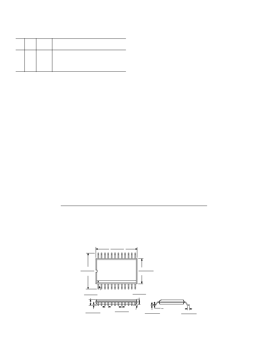
24-Lead Shrink Small Outline Package
(RS-24)
24
1
13
12
0.328 (8.33)
0.318 (8.08)
0.311 (7.9)
0.301 (7.64)
0.212 (5.38)
0.205 (5.207)
PIN 1
SEATING
PLANE
0.07 (1.78)
0.066 (1.67)
0.008 (0.203)
0.002 (0.050)
0.0256
(0.65)
BSC
0.078 (1.98)
0.068 (1.73)
0.015 (0.38)
0.010 (0.25)
0.009 (0.229)
0.005 (0.127)
0.037 (0.94)
0.022 (0.559)
8°
0°