Äîêóìåíòàöèÿ è îïèñàíèÿ www.docs.chipfind.ru
Single-Phase Active and Apparent
Energy Metering IC
ADE7763
Rev. A
Information furnished by Analog Devices is believed to be accurate and reliable.
However, no responsibility is assumed by Analog Devices for its use, nor for any
infringements of patents or other rights of third parties that may result from its use.
Specifications subject to change without notice. No license is granted by implication
or otherwise under any patent or patent rights of Analog Devices. Trademarks and
registered trademarks are the property of their respective owners.
One Technology Way, P.O. Box 9106, Norwood, MA 02062-9106, U.S.A.
Tel: 781.329.4700
www.analog.com
Fax: 781.326.8703
© 2004 Analog Devices, Inc. All rights reserved.
FEATURES
High accuracy; supports IEC 61036/60687, IEC62053-21, and
IEC62053-22
On-chip digital integrator enables direct interface-to-current
sensors with di/dt output
A PGA in the current channel allows direct interface to
shunts and current transformers
Active and apparent energy, sampled waveform, and current
and voltage rms
Less than 0.1% error in active energy measurement over a
dynamic range of 1000 to 1 at 25°C
Positive-only energy accumulation mode available
On-chip user programmable threshold for line voltage surge
and SAG and PSU supervisory
Digital calibration for power, phase, and input offset
On-chip temperature sensor (±3°C typical)
SPI®-compatible serial interface
Pulse output with programmable frequency
Interrupt request pin (IRQ) and status register
Reference 2.4 V with external overdrive capability
Single 5 V supply, low power (25 mW typical)
GENERAL DESCRIPTION
The ADE7763
1
features proprietary ADCs and fixed function
DSP for high accuracy over large variations in environmental
conditions and time. The ADE7763 incorporates two second-
order, 16-bit - ADCs, a digital integrator (on Ch1), reference
circuitry, a temperature sensor, and all the signal processing
required to perform active and apparent energy measurements,
line-voltage period measurements, and rms calculation on the
voltage and current channels. The selectable on-chip digital
integrator provides direct interface to di/dt current sensors such
as Rogowski coils, eliminating the need for an external analog
integrator and resulting in excellent long-term stability and
precise phase matching between the current and the voltage
channels.
The ADE7763 provides a serial interface to read data and a
pulse output frequency (CF) that is proportional to the active
power. Various system calibration features such as channel
offset correction, phase calibration, and power calibration
ensure high accuracy. The part also detects short duration, low
or high voltage variations.
The positive-only accumulation mode gives the option to
accumulate energy only when positive power is detected. An
internal no-load threshold ensures that the part does not exhibit
any creep when there is no load. The zero-crossing output (ZX)
produces a pulse that is synchronized to the zero-crossing point
of the line voltage. This signal is used internally in the line cycle
active and apparent energy accumulation modes, which enables
faster calibration.
The interrupt status register indicates the nature of the interrupt,
and the interrupt enable register controls which event produces
an output on the IRQ pin, an open-drain, active low logic output.
The ADE7763 is available in a 20-lead SSOP package.
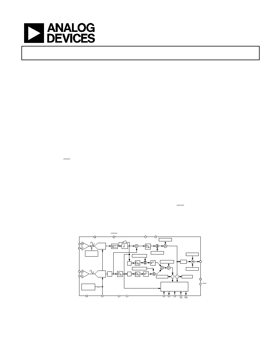
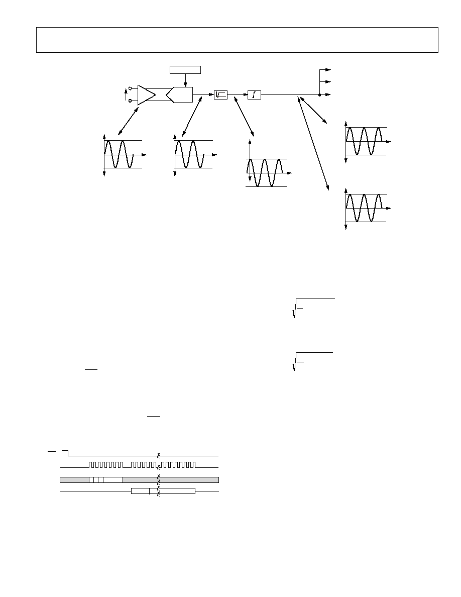
FUNCTIONAL BLOCK DIAGRAM
AVDD
RESET
DVDD
DGND
TEMP
SENSOR
ADC
ADC
DFC
x
2
ADE7763
LPF2
MULTIPLIER
INTEGRATOR
CLKIN CLKOUT
DIN DOUT SCLK
REF
IN/OUT
CS IRQ
AGND
APOS[15:0]
VAGAIN[11:0]
VADIV[7:0]
IRMSOS[11:0]
VRMSOS[11:0]
WGAIN[11:0]
dt
REGISTERS AND
SERIAL INTERFACE
CFNUM[11:0]
CFDEN[11:0]
2.4V
REFERENCE
4k
PHCAL[5:0]
HPF1
LPF1
04481-
A
-
001
V1P
V1N
V2N
V2P
PGA
PGA
ZX
SAG
CF
WDIV[7:0]
%
%
x
2
Figure 1.
1
U.S. Patents 5,745,323; 5,760,617; 5,862,069; 5,872,469; others pending.

ADE7763
Rev. A | Page 2 of 56
TABLE OF CONTENTS
Specifications..................................................................................... 3
Timing Characteristics..................................................................... 5
Absolute Maximum Ratings............................................................ 6
ESD Caution.................................................................................. 6
Terminology ...................................................................................... 7
Pin Configuration and Function Descriptions............................. 8
Typical Performance Characteristics ........................................... 10
Theory of Operation ...................................................................... 13
Analog Inputs.............................................................................. 13
di/dt Current Sensor and Digital Integrator ........................... 14
Zero-Crossing Detection........................................................... 15
Period Measurement .................................................................. 16
Power Supply Monitor ............................................................... 16
Line Voltage Sag Detection ....................................................... 17
Peak Detection ............................................................................ 17
Interrupts..................................................................................... 18
Temperature Measurement ....................................................... 19
Analog-to-Digital Conversion.................................................. 19
Channel 1 ADC .......................................................................... 20
Channel 2 ADC .......................................................................... 22
Phase Compensation.................................................................. 24
Active Power Calculation .......................................................... 25
Energy Calculation..................................................................... 26
Power Offset Calibration ........................................................... 28
Energy-to-Frequency Conversion............................................ 28
Line Cycle Energy Accumulation Mode ................................. 30
Positive-Only Accumulation Mode ......................................... 30
No-Load Threshold.................................................................... 30
Apparent Power Calculation..................................................... 31
Apparent Energy Calculation ................................................... 32
Line Apparent Energy Accumulation...................................... 33
Energies Scaling.......................................................................... 34
Calibrating an Energy Meter .................................................... 34
CLKIN Frequency ...................................................................... 43
Suspending Functionality.......................................................... 44
Checksum Register..................................................................... 44
Serial Interface ............................................................................ 44
Registers........................................................................................... 47
Register Descriptions ..................................................................... 50
Communication Register .......................................................... 50
Mode Register (0x09)................................................................. 50
Interrupt Status Register (0x0B), Reset Interrupt Status
Register (0x0C), Interrupt Enable Register (0x0A) ............... 52
CH1OS Register (0x0D)............................................................ 53
Outline Dimensions ....................................................................... 54
Ordering Guide .......................................................................... 54
REVISION HISTORY
10/04--Data Sheet Changed from Rev. 0 to Rev. A
Changes to Period Measurement Section ..................................16
Changes to Temperature Measurement Section........................19
Change to Energy-to-Frequency Conversion Section..............28
Update to Figure 61 .......................................................................29
Change to Apparent Energy Calculation Section .....................32
Change to Description of AEHF and VAEHF Bits ...................52
4/04--Revision 0: Initial Version

ADE7763
Rev. A | Page 3 of 56
SPECIFICATIONS
AV
DD
= DV
DD
= 5 V ± 5%, AGND = DGND = 0 V, on-chip reference, CLKIN = 3.579545 MHz XTAL, T
MIN
to T
MAX
= 40°C to +85°C.
Table 1. Specifications
1, 2
Parameter Spec
Unit
Test
Conditions/Comments
ENERGY MEASUREMENT ACCURACY
Active Power Measurement Error
CLKIN = 3.579545 MHz
Channel 1 Range = 0.5 V Full Scale
Channel 2 = 300 mV rms/60 Hz, gain = 2
Gain = 1
0.1
% typ
Over a dynamic range 1000 to 1
Gain = 2
0.1
% typ
Over a dynamic range 1000 to 1
Gain = 4
0.1
% typ
Over a dynamic range 1000 to 1
Gain = 8
0.1
% typ
Over a dynamic range 1000 to 1
Channel 1 Range = 0.25 V Full Scale
Gain = 1
0.1
% typ
Over a dynamic range 1000 to 1
Gain = 2
0.1
% typ
Over a dynamic range 1000 to 1
Gain = 4
0.1
% typ
Over a dynamic range 1000 to 1
Gain = 8
0.2
% typ
Over a dynamic range 1000 to 1
Channel 1 Range = 0.125 V Full Scale
Gain = 1
0.1
% typ
Over a dynamic range 1000 to 1
Gain = 2
0.1
% typ
Over a dynamic range 1000 to 1
Gain = 4
0.2
% typ
Over a dynamic range 1000 to 1
Gain = 8
0.2
% typ
Over a dynamic range 1000 to 1
Active Power Measurement Bandwidth
14
kHz
Phase Error 1 between Channels
±0.05
max
Line frequency = 45 Hz to 65 Hz, HPF on
AC Power Supply Rejection
1
AVDD = DVDD = 5 V + 175 mV rms/120 Hz
Output Frequency Variation (CF)
0.2
% typ
Channel 1 = 20 mV rms, gain = 16, range = 0.5 V
Channel 2 = 300 mV rms/60 Hz, gain = 1
DC Power Supply Rejection
1
AVDD = DVDD = 5 V ± 250 mV dc
Output Frequency Variation (CF)
±0.3
% typ
Channel 1 = 20 mV rms/60 Hz, gain = 16, range = 0.5 V
Channel 2 = 300 mV rms/60 Hz, gain = 1
IRMS Measurement Error
0.5
% typ
Over a dynamic range 100 to 1
IRMS Measurement Bandwidth
14
kHz
VRMS Measurement Error
0.5
% typ
Over a dynamic range 20 to 1
VRMS Measurement Bandwidth
140
Hz
ANALOG INPUTS
3
See the Analog Inputs section
Maximum Signal Levels
±0.5
V max
V1P, V1N, V2N, and V2P to AGND
Input Impedance (dc)
390
k min
Bandwidth
14
kHz
CLKIN/256, CLKIN = 3.579545 MHz
Gain Error
1, 3
External 2.5 V reference, gain = 1 on Channels 1 and 2
Channel 1
Range = 0.5 V Full Scale
±4
% typ
V1 = 0.5 V dc
Range = 0.25 V Full Scale
±4
% typ
V1 = 0.25 V dc
Range = 0.125 V Full Scale
±4
% typ
V1 = 0.125 V dc
Channel 2
±4
% typ
V2 = 0.5 V dc
Offset Error 1
±32
mV max
Gain 1
Channel 1
±13
mV max
Gain 16
±32
mV max
Gain 1
Channel 2
±13
mV max
Gain 16

ADE7763
Rev. A | Page 4 of 56
Parameter Spec
Unit
Test
Conditions/Comments
WAVEFORM SAMPLING
Sampling CLKIN/128, 3.579545 MHz/128 = 27.9 kSPS
Channel 1
See the Channel 1 Sampling section
Signal-to-Noise Plus Distortion
62
dB typ
150 mV rms/60 Hz, range = 0.5 V, gain = 2
Bandwidth (3 dB)
14
kHz
CLKIN = 3.579545 MHz
Channel 2
See the Channel 2 Sampling section
Signal-to-Noise Plus Distortion
60
dB typ
150 mV rms/60 Hz, gain = 2
Bandwidth (3 dB)
140
Hz
CLKIN = 3.579545 MHz
REFERENCE INPUT
REF
IN/OUT
Input Voltage Range
2.6
V max
2.4 V + 8%
2.2
V min
2.4 V 8%
Input Capacitance
10
pF max
ON-CHIP REFERENCE
Nominal 2.4 V at REF
IN/OUT
pin
Reference Error
±200
mV max
Current Source
10
µA max
Output Impedance
3.4
k min
Temperature Coefficient
30
ppm/°C typ
CLKIN
All specifications CLKIN of 3.579545 MHz
Input Clock Frequency
4
MHz max
1
MHz
min
LOGIC INPUTS
RESET, DIN, SCLK, CLKIN, and CS
Input High Voltage, V
INH
2.4
V min
DVDD = 5 V ± 10%
Input Low Voltage, V
INL
0.8
V max
DVDD = 5 V ± 10%
Input Current, I
IN
±3
µA max
Typically 10 nA, V
IN
= 0 V to DVDD
Input Capacitance, C
IN
10 pF
max
LOGIC OUTPUTS
SAG and IRQ
Open-drain outputs, 10 k pull-up resistor
Output High Voltage, V
OH
4 V
min
I
SOURCE
= 5 mA
Output Low Voltage, V
OL
0.4 V
max
I
SINK
= 0.8 mA
ZX and DOUT
Output High Voltage, V
OH
4 V
min
I
SOURCE
= 5 mA
Output Low Voltage, V
OL
0.4 V
max
I
SINK
= 0.8 mA
CF
Output High Voltage, V
OH
4 V
min
I
SOURCE
= 5 mA
Output Low Voltage, V
OL
1 V
max
I
SINK
= 7 mA
POWER SUPPLY
For specified performance
AVDD
4.75
V min
5 V 5%
5.25
V max
5 V + 5%
DVDD
4.75
V min
5 V 5%
5.25
V max
5 V + 5%
AIDD
3
mA max
Typically 2.0 mA
DIDD
4
mA max
Typically 3.0 mA
__________________________________________________________
1
See the Terminology section for explanation of specifications.
2
See the plots in the Typical Performance Characteristics section.
3
See the Analog Inputs section.
+2.1V
1.6mA
I
OH
I
Ol
200
µ
A
C
L
50pF
04481-A
-
002
TO
OUTPUT
PIN
Figure 2. Load Circuit for Timing Specifications
ADE7763
Rev. A | Page 5 of 56
TIMING CHARACTERISTICS
AV
DD
= DV
DD
= 5 V ± 5%, AGND = DGND = 0 V, on-chip reference, CLKIN = 3.579545 MHz XTAL, T
MIN
to T
MAX
= -40°C to +85°C.
Table 2. Timing Characteristics
1, 2
Parameter Spec Unit Test
Conditions/Comments
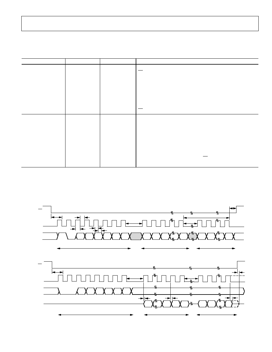
Write Timing
t
1
50 ns
min
CS falling edge to first SCLK falling edge.
t
2
50
ns min
SCLK logic high pulse width.
t
3
50
ns min
SCLK logic low pulse width.
t
4
10
ns min
Valid data setup time before falling edge of SCLK.
t
5
5
ns min
Data hold time after SCLK falling edge.
t
6
400
ns min
Minimum time between the end of data byte transfers.
t
7
50
ns min
Minimum time between byte transfers during a serial write.
t
8
100 ns
min)
CS hold time after SCLK falling edge.
Read Timing
t
9
3
4 µs
min
Minimum time between read command (i.e., a write to
communication register) and data read.
t
10
50
ns min
Minimum time between data byte transfers during a multibyte read.
t
11
30 ns
min
Data access time after SCLK rising edge following a write to the
communication register.
t
12
4
100
ns max
Bus relinquish time after falling edge of SCLK.
10
ns
min
t
13
5
100 ns
max
Bus relinquish time after rising edge of CS.
10
ns
min
________________________________________________
1
Sample tested during initial release and after any redesign or process change that could affect this parameter. All input signals are specified with tr = tf = 5 ns (10% to
90%) and timed from a voltage level of 1.6 V.
2
See Figure 3, Figure 4, and the Serial Interface section.
3
Minimum time between read command and data read for all registers except waveform register, which is t
9
= 500 ns min.
4
Measured with the load circuit in Figure 2 and defined as the time required for the output to cross 0.8 V or 2.4 V.
5
Derived from the measured time taken by the data outputs to change 0.5 V when loaded with the circuit in Figure 2. The measured number is then extrapolated back
to remove the effects of charging or discharging the 50 pF capacitor. This means that the time quoted in the timing characteristics is the true bus relinquish time of
the part and is independent of the bus loading.
DIN
SCLK
CS
t
2
t
3
t
1
t
4
t
5
t
7
t
6
t
8
COMMAND BYTE
MOST SIGNIFICANT BYTE
LEAST SIGNIFICANT BYTE
1
0
A4
A5
A3
A2
A1
A0
DB7
DB0
DB7
DB0
t
7
04481-A
-
003
Figure 3. Serial Write Timing
SCLK
CS
t
1
t
10
t
13
0
0
A4
A5
A3
A2
A1
A0
DB0
DB7
DB0
DB7
DIN
DOUT
t
11
t
11
t
12
COMMAND BYTE
MOST SIGNIFICANT BYTE
LEAST SIGNIFICANT BYTE
t
9
04481-A
-
004
Figure 4. Serial Read Timing

ADE7763
Rev. A | Page 6 of 56
ABSOLUTE MAXIMUM RATINGS
T
A
= 25°C, unless otherwise noted.
Table 3.
Parameter Rating
AVDD to AGND
0.3 V to +7 V
DVDD to DGND
0.3 V to +7 V
DVDD to AVDD
0.3 V to +0.3 V
Analog Input Voltage to AGND
V1P, V1N, V2P, and V2N
6 V to +6 V
Reference Input Voltage to AGND
0.3 V to AVDD + 0.3 V
Digital Input Voltage to DGND
0.3 V to DVDD + 0.3 V
Digital Output Voltage to DGND
0.3 V to DVDD + 0.3 V
Operating Temperature Range
Industrial
40°C to +85°C
Storage Temperature Range
65°C to +150°C
Junction Temperature
150°C
20-Lead SSOP, Power Dissipation
450 mW
JA
Thermal Impedance
112°C/W
Lead Temperature, Soldering
Vapor Phase (60 s)
215°C
Infrared (15 s)
220°C
Stresses above those listed under Absolute Maximum Ratings
may cause permanent damage to the device. This is a stress
rating only, and functional operation of the device at these or
any other conditions above those indicated in the operational
section of this specification is not implied. Exposure to absolute
maximum rating conditions for extended periods may affect
device reliability.
ESD CAUTION
ESD (electrostatic discharge) sensitive device. Electrostatic charges as high as 4000 V readily accumulate on
the human body and test equipment and can discharge without detection. Although this product features
proprietary ESD protection circuitry, permanent damage may occur on devices subjected to high energy
electrostatic discharges. Therefore, proper ESD precautions are recommended to avoid performance
degradation or loss of functionality.

ADE7763
Rev. A | Page 7 of 56
TERMINOLOGY
Measurement Error
The error associated with the energy measurement made by the
ADE7763 is defined by the following formula:
Percent Error =
-
Energy
True
Energy
True
ADE7763
Register
Energy
× 100%
Phase Error between Channels
The digital integrator and the high-pass filter (HPF) in Channel 1
have a nonideal phase response. To offset this phase response
and equalize the phase response between channels, two phase-
correction networks are placed in Channel 1: one for the digital
integrator and the other for the HPF. The phase correction
networks correct the phase response of the corresponding
component and ensure a phase match between Channel 1
(current) and Channel 2 (voltage) to within ±0.1° over a range
of 45 Hz to 65 Hz with the digital integrator off. With the digital
integrator on, the phase is corrected to within ±0.4° over a
range of 45 Hz to 65 Hz.
Power Supply Rejection
This quantifies the ADE7763 measurement error as a percentage
of the reading when the power supplies are varied. For the ac
PSR measurement, a reading at nominal supplies (5 V) is taken.
A second reading is obtained with the same input signal levels
when an ac (175 mV rms/120 Hz) signal is introduced to the
supplies. Any error introduced by this ac signal is expressed
as a percentage of the reading--see the Measurement
Error definition.
For the dc PSR measurement, a reading at nominal supplies
(5 V) is taken. A second reading is obtained with the same input
signal levels when the supplies are varied ±5%. Any error
introduced is again expressed as a percentage of the reading.
ADC Offset Error
The dc offset associated with the analog inputs to the ADCs. It
means that with the analog inputs connected to AGND, the
ADCs still see a dc analog input signal. The magnitude of the
offset depends on the gain and input range selection--see the
Typical Performance Characteristics section. However, when
HPF1 is switched on, the offset is removed from Channel 1
(current) and the power calculation is not affected by this offset.
The offsets can be removed by performing an offset calibration--
see the Analog Inputs section.
Gain Error
The difference between the measured ADC output code (minus
the offset) and the ideal output code--see the Channel 1 ADC
and Channel 2 ADC sections. It is measured for each of the
input ranges on Channel 1 (0.5 V, 0.25 V, and 0.125 V). The
difference is expressed as a percentage of the ideal code.
ADE7763
Rev. A | Page 8 of 56
PIN CONFIGURATION AND FUNCTION DESCRIPTIONS
V2N
6
V2P
7
AGND
8
REF
IN/OUT
9
DGND
10
CLKIN
IRQ
SAG
ZX
CF
15
14
13
12
11
ADE7763
TOP VIEW
(Not to Scale)
DVDD
2
AVDD
3
V1P
4
V1N
5
DOUT
SCLK
CS
CLKOUT
19
18
RESET
1
DIN
20
17
16
04481-A
-
005
Figure 5. Pin Configuration (SSOP Package)
Table 4. Pin Function Descriptions
Pin No.
Mnemonic
Description
1
RESET
Reset Pin for the ADE7763. A logic low on this pin holds the ADCs and digital circuitry (including the serial
interface) in a reset condition.
2 DVDD Digital Power Supply. This pin provides the supply voltage for the digital circuitry. The supply voltage
should be maintained at 5 V ± 5% for specified operation. This pin should be decoupled to DGND with a
10 µF capacitor in parallel with a ceramic 100 nF capacitor.
3 AVDD Analog Power Supply. This pin provides the supply voltage for the analog circuitry. The supply should be
maintained at 5 V ± 5% for specified operation. Minimize power supply ripple and noise at this pin by using
proper decoupling. The typical performance graphs show the power supply rejection performance. This
pin should be decoupled to AGND with a 10 µF capacitor in parallel with a ceramic 100 nF capacitor.
4, 5
V1P, V1N
Analog Inputs for Channel 1. This channel is intended for use with a di/dt current transducer, i.e., a
Rogowski coil or another current sensor such as a shunt or current transformer (CT). These inputs are fully
differential voltage inputs with maximum differential input signal levels of ±0.5 V, ±0.25 V, and ±0.125 V,
depending on the full-scale selection--see the Analog Inputs section. Channel 1 also has a PGA with gain
selections of 1, 2, 4, 8, or 16. The maximum signal level at these pins with respect to AGND is ±0.5 V. Both
inputs have internal ESD protection circuitry and can sustain an overvoltage of ±6 V without risk of
permanent damage.
6, 7
V2N, V2P
Analog Inputs for Channel 2. This channel is intended for use with the voltage transducer. These inputs are
fully differential voltage inputs with a maximum differential signal level of ±0.5 V. Channel 2 also has a PGA
with gain selections of 1, 2, 4, 8, or 16. The maximum signal level at these pins with respect to AGND is
±0.5 V. Both inputs have internal ESD protection circuitry and can sustain an overvoltage of ±6 V without
risk of permanent damage.
8 AGND
Analog Ground Reference. This pin provides the ground reference for the analog circuitry, i.e., ADCs and
reference. This pin should be tied to the analog ground plane or to the quietest ground reference in the
system. Use this quiet ground reference for all analog circuitry, such as antialiasing filters and current and
voltage transducers. To minimize ground noise around the ADE7763, connect the quiet ground plane
to the digital ground plane at only one point. It is acceptable to place the entire device on the analog
ground plane.
9 REF
IN/OUT
Access to the On-Chip Voltage Reference. The on-chip reference has a nominal value of 2.4 V ± 8% and a
typical temperature coefficient of 30 ppm/°C. An external reference source can also be connected at this
pin. In either case, this pin should be decoupled to AGND with a 1 µF ceramic capacitor.
10 DGND Digital Ground Reference. This pin provides the ground reference for the digital circuitry, i.e., multiplier,
filters, and digital-to-frequency converter. Because the digital return currents in the ADE7763 are small, it is
acceptable to connect this pin to the analog ground plane of the system. However, high bus capacitance
on the DOUT pin could result in noisy digital current, which could affect performance.
11 CF
Calibration Frequency Logic Output. The CF logic output gives active power information. This output is
intended to be used for operational and calibration purposes. The full-scale output frequency can be
adjusted by writing to the CFDEN and CFNUM registers--see the Energy-to-Frequency Conversion section.
12 ZX
Voltage Waveform (Channel 2) Zero-Crossing Output. This output toggles logic high and logic low at the
zero crossing of the differential signal on Channel 2--see the Zero-Crossing Detection section.
13
SAG
This open-drain logic output goes active low when either no zero crossings are detected or a low voltage
threshold (Channel 2) is crossed for a specified duration--see the Line Voltage Sag Detection section.
14
IRQ
Interrupt Request Output. This is an active low, open-drain logic output. Maskable interrupts include active
energy register rollover, active energy register at half level, and arrivals of new waveform samples--see the
Interrupts section.

ADE7763
Rev. A | Page 9 of 56
Pin No.
Mnemonic
Description
15 CLKIN Master Clock for ADCs and Digital Signal Processing. An external clock can be provided at this logic input.
Alternatively, a parallel resonant AT crystal can be connected across CLKIN and CLKOUT to provide a clock
source for the ADE7763. The clock frequency for specified operation is 3.579545 MHz. Ceramic load
capacitors between 22 pF and 33 pF should be used with the gate oscillator circuit. Refer to the crystal
manufacturer's data sheet for load capacitance requirements.
16 CLKOUT
A crystal can be connected across this pin and CLKIN, as described for Pin 15, to provide a clock source for
the ADE7763. The CLKOUT pin can drive one CMOS load when either an external clock is supplied at CLKIN
or a crystal is being used.
17
CS
Chip Select. Part of the 4-wire SPI serial interface. This active low logic input allows the ADE7763 to share
the serial bus with several other devices--see the Serial Interface section.
18 SCLK Serial Clock Input for the Synchronous Serial Interface. All serial data transfers are synchronized to this
clock--see the Serial Interface section. The SCLK has a Schmitt-trigger input for use with a clock source
that has a slow edge transition time, such as an opto-isolator output.
19 DOUT Data Output for the Serial Interface. Data is shifted out at this pin upon the rising edge of SCLK. This logic
output is normally in a high impedance state, unless it is driving data onto the serial data bus--see the
Serial Interface section.
20 DIN
Data Input for the Serial Interface. Data is shifted in at this pin upon the falling edge of SCLK--see the
Serial Interface section.
ADE7763
Rev. A | Page 10 of 56
TYPICAL PERFORMANCE CHARACTERISTICS
FULL-SCALE CURRENT (%)
E
RROR (%)
0.1
0.6
0.2
0.3
0.4
0.5
0.1
0
0.4
0.3
0.2
0.1
1
10
100
04481-A
-
006
GAIN = 1
INTEGRATOR OFF
INTERNAL REFERENCE
40°C, PF = 0.5
+85°C, PF = 0.5
+25°C, PF = 0.5
+25°C, PF = 1
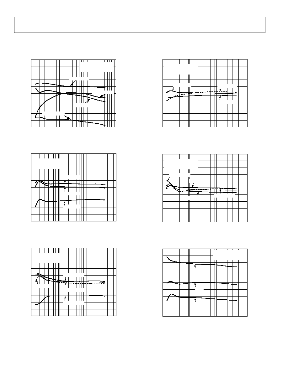
Figure 6. Active Energy Error as a Percentage of Reading (Gain = 1)
over Power Factor with Internal Reference and Integrator Off
1.0
0.8
0.6
0.4
0.2
0
0.2
0.4
0.6
0.8
1.0
E
RROR (%)
FULL-SCALE CURRENT (%)
0.1
10
1
100
04481-A
-
007
GAIN = 8
INTEGRATOR OFF
INTERNAL REFERENCE
+85°C, PF = 1
+25°C, PF = 1
40°C, PF = 1
Figure 7. Active Energy as a Percentage of Reading (Gain = 8)
over Temperature with Internal Reference and Integrator Off
1.0
0.8
0.6
0.4
0.2
0
0.2
0.4
0.6
0.8
1.0
E
RROR (%)
FULL-SCALE CURRENT (%)
0.1
10
1
100
04481-A
-
008
GAIN = 8
INTEGRATOR OFF
INTERNAL REFERENCE
+85°C, PF = 0.5
+25°C, PF = 0.5
40°C, PF = 0.5
+25°C, PF = 1
Figure 8. Active Energy Error as a Percentage of Reading (Gain = 8)
over Power Factor with Internal Reference and Integrator Off
1.0
0.8
0.6
0.4
0.2
0
0.2
0.4
0.6
0.8
1.0
E
RROR (%)
FULL-SCALE CURRENT (%)
0.1
10
1
100
04481-A
-
009
GAIN = 8
INTEGRATOR OFF
EXTERNAL REFERENCE
+85°C, PF = 1
40°C, PF = 1
+25°C, PF = 1
Figure 9. Active Energy Error as a Percentage of Reading (Gain = 8)
over Temperature with External Reference and Integrator Off
1.0
0.8
0.6
0.4
0.2
0
0.2
0.4
0.6
0.8
1.0
E
RROR (%)
FULL-SCALE CURRENT (%)
0.1
10
1
100
04481-A
-
010
GAIN = 8
INTEGRATOR OFF
EXTERNAL REFERENCE
+85°C, PF = 0.5
+25°C, PF = 0.5
40°C, PF = 0.5
+25°C, PF = 1
Figure 10. Active Energy Error as a Percentage of Reading (Gain = 8)
over Power Factor with External Reference and Integrator Off
0.5
0.4
0.3
0.2
0.1
0
0.1
0.2
0.3
0.4
0.5
E
RROR (%)
FULL-SCALE CURRENT (%)
0.1
10
1
100
04481-A
-
080
GAIN = 8
INTEGRATOR OFF
INTERNAL REFERENCE
5.25V
5.00V
4.75V
Figure 11. Active Energy Error as a Percentage of Reading (Gain = 8)
over Power Supply with Internal Reference and Integrator Off
ADE7763
Rev. A | Page 11 of 56
0.6
0.4
0.2
0
0.2
0.4
0.6
0.8
1.0
1.2
E
RROR (%)
45
47
49
51
53
55
57
59
61
63
65
FREQUENCY (Hz)
04481-A
-
012
GAIN = 8
INTEGRATOR OFF
INTERNAL REFERENCE
PF = 0.5
PF = 1
Figure 12. Active Energy Error as a Percentage of Reading (Gain = 8)
over Frequency with Internal Reference and Integrator Off
1.0
0.8
0.6
0.4
0.2
0
0.2
0.4
0.6
0.8
1.0
E
RROR (%)
FULL-SCALE CURRENT (%)
0.1
10
1
100
04481-A
-
013
GAIN = 8
INTEGRATOR OFF
INTERNAL REFERENCE
PF = 1
PF = 0.5
Figure 13. IRMS Error as a Percentage of Reading (Gain = 8)
with Internal Reference and Integrator Off
0.5
0.4
0.3
0.2
0.1
0
0.1
0.2
0.3
0.4
0.5
E
RROR (%)
FULL-SCALE VOLTAGE (%)
1
10
100
04481-A
-
020
GAIN = 1
EXTERNAL REFERENCE
Figure 14. VRMS Error as a Percentage of Reading (Gain = 1)
with External Reference
1.0
0.8
0.6
0.4
0.2
0
0.2
0.4
0.6
0.8
1.0
E
RROR (%)
FULL-SCALE CURRENT (%)
0.1
10
1
100
04481-A
-
016
GAIN = 8
INTEGRATOR ON
INTERNAL REFERENCE
+85°C, PF = 0.5
+25°C, PF = 1
40°C, PF = 0.5
+25°C, PF = 0.5
Figure 15. Active Energy Error as a Percentage of Reading (Gain = 8)
over Power Factor with Internal Reference and Integrator On
1.0
0.8
0.6
0.4
0.2
0
0.2
0.4
0.6
0.8
1.0
E
RROR (%)
FULL-SCALE CURRENT (%)
0.1
10
1
100
04481-A
-
015
GAIN = 8
INTEGRATOR ON
INTERNAL REFERENCE
+85°C, PF = 1
+25°C, PF = 1
40°C, PF = 1
Figure 16. Active Energy Error as a Percentage of Reading (Gain = 8)
over Temperature with External Reference and Integrator On
2.0
1.5
1.0
0.5
0
0.5
1.0
1.5
2.0
2.5
3.0
E
RROR (%)
45
47
49
51
53
55
57
59
61
63
65
FREQUENCY (Hz)
04481-A
-
017
GAIN = 8
INTEGRATOR ON
INTERNAL REFERENCE
PF = 0.5
PF = 1
Figure 17. Active Energy Error as a Percentage of Reading (Gain = 8)
over Frequency with Internal Reference and Integrator On

ADE7763
Rev. A | Page 12 of 56
0.5
0.4
0.3
0.2
0.1
0
0.1
0.2
0.3
0.4
0.5
E
RROR (%)
FULL-SCALE CURRENT (%)
0.1
10
1
100
04481-A
-
081
GAIN = 8
INTEGRATOR ON
INTERNAL REFERENCE
5.25V
5.00V
4.75V
Figure 18. Active Energy Error as a Percentage of Reading (Gain = 8)
over Power Supply with Internal Reference and Integrator On
0.5
0.4
0.3
0.2
0.1
0
0.1
0.2
0.3
0.4
0.5
E
RROR (%)
FULL-SCALE CURRENT (%)
0.1
10
1
100
04481-A
-
019
GAIN = 8
INTEGRATOR ON
INTERNAL REFERENCE
PF = 0.5
PF = 1
Figure 19. IRMS Error as a Percentage of Reading (Gain = 8)
with Internal Reference and Integrator On
0
2
4
6
8
10
HITS
12
14
16
15
10
5
0
5
10
15
20
CH1 OFFSET (0p5V_1X) (mV)
04481-A
-
021
Figure 20. Channel 1 Offset (Gain = 1)
V
DD
10
µ
F
10
µ
F
10
µ
F
100nF
100nF
AVDD DVDD RESET
DIN
DOUT
SCLK
CS
CLKOUT
CLKIN
IRQ
SAG
ZX
CF
AGND DGND
V1P
V1N
V2N
V2P
REF
IN/OUT
U1
ADE7763
TO SPI BUS
(USED ONLY FOR
CALIBRATION)
22pF
22pF
Y1
3.58MHz
NOT CONNECTED
U3
PS2501-1
I
di/dt CURRENT
SENSOR
100
1k
33nF
33nF
100
1k
33nF
33nF
1k
33nF
600k
110V
1k
33nF
100nF
CHANNEL 1 GAIN = 8
CHANNEL 2 GAIN = 1
TO
FREQUENCY
COUNTER
04481-A
-
022
Figure 21. Test Circuit for Performance Curves with Integrator On
CT TURN RATIO = 1800:1
CHANNEL 2 GAIN = 1
RB
10
1.21
GAIN 1 (CH1)
1
8
NOT CONNECTED
V
DD
10
µ
F
1
µ
F
100nF
100nF
DIN
DOUT
SCLK
CS
CLKOUT
CLKIN
IRQ
SAG
ZX
CF
AGND DGND
V1P
V1N
V2N
V2P
REF
IN/OUT
U1
ADE7763
TO SPI BUS
(USED ONLY FOR
CALIBRATION)
22pF
22pF
Y1
3.58MHz
U3
PS2501-1
I
CURRENT
TRANSFORMER
1k
33nF
1k
33nF
1k
33nF
600k
0
RB
110V
1k
33nF
10
µ
F
100nF
TO
FREQUENCY
COUNTER
04481-A
-
023
AVDD DVDD RESET
Figure 22. Test Circuit for Performance Curves with Integrator Off
ADE7763
Rev. A | Page 13 of 56
THEORY OF OPERATION
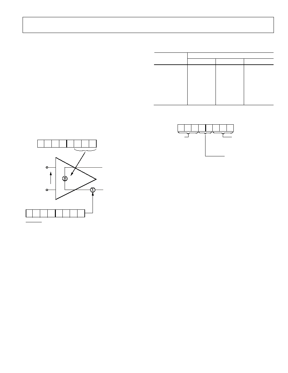
ANALOG INPUTS
The ADE7763 has two fully differential voltage input channels.
The maximum differential input voltage for input pairs V1P/V1N
and V2P/V2N is ±0.5 V. In addition, the maximum signal level
on analog inputs for V1P/V1N and V2P/V2N is ±0.5 V with
respect to AGND.
Each analog input channel has a programmable gain amplifier
(PGA) with possible gain selections of 1, 2, 4, 8, and 16. The
gain selections are made by writing to the gain register--see
Figure 24. Bits 0 to 2 select the gain for the PGA in Channel 1;
the gain selection for the PGA in Channel 2 is made via Bits 5
to 7. Figure 23 shows how a gain selection for Channel 1 is
made using the gain register.
V1P
V1N
V
IN
K
×
V
IN
+
GAIN[7:0]
7
6
5
4
3
2
1
0
0
0
0
0
0
0
0
0
7
6
5
4
3
2
1
0
0
0
0
0
0
0
0
0
GAIN (K)
SELECTION
OFFSET ADJUST
(±50mV)
CH1OS[7:0]
BITS 0 to 5: SIGN MAGNITUDE CODED OFFSET CORRECTION
BIT 6: NOT USED
BIT 7: DIGITAL INTEGRATOR (ON = 1, OFF = 0; DEFAULT OFF)
04481-A
-
024
Figure 23. PGA in Channel 1
In addition to the PGA, Channel 1 also has a full-scale input
range selection for the ADC. The ADC analog input range
selection is also made using the gain register--see Figure 24. As
previously mentioned, the maximum differential input voltage
is 0.5 V. However, by using Bits 3 and 4 in the gain register, the
maximum ADC input voltage can be set to 0.5 V, 0.25 V, or
0.125 V. This is achieved by adjusting the ADC reference--see
the Reference Circuit section. Table 5 summarizes the
maximum differential input signal level on Channel 1 for the
various ADC range and gain selections.
Table 5. Maximum Input Signal Levels for Channel 1
ADC Input Range Selection
Max Signal
Channel 1
0.5 V
0.25 V
0.125 V
0.5 V
Gain = 1
-
-
0.25 V
Gain = 2
Gain = 1
-
0.125 V
Gain = 4
Gain = 2
Gain = 1
0.0625 V
Gain = 8
Gain = 4
Gain = 2
0.0313 V
Gain = 16
Gain = 8
Gain = 4
0.0156 V
-
Gain = 16
Gain = 8
0.00781 V
-
-
Gain = 16
GAIN REGISTER*
CHANNEL 1 AND CHANNEL 2 PGA CONTROL
7 6 5 4 3 2 1 0
0 0 0 0 0 0 0 0
ADDR:
0x0A
* REGISTER CONTENTS
SHOW POWER-ON DEFAULTS
PGA 2 GAIN SELECT
000 =
×
1
001 =
×
2
010 =
×
4
011 =
×
8
100 =
×
16
PGA 1 GAIN SELECT
000 =
×
1
001 =
×
2
010 =
×
4
011 =
×
8
100 =
×
16
CHANNEL 1 FULL-SCALE SELECT
00 = 0.5V
01 = 0.25V
10 = 0.125V
04481-A-025
Figure 24. Analog Gain Register
It is also possible to adjust offset errors on Channel 1 and
Channel 2 by writing to the offset correction registers (CH1OS
and CH2OS, respectively). These registers allow channel offsets
in the range ±20 mV to ±50 mV (depending on the gain setting)
to be removed. Note that it is not necessary to perform an offset
correction in an energy measurement application if HPF in
Channel 1 is switched on. Figure 25 shows the effect of offsets
on the real power calculation. As seen from Figure 25, an offset
on Channel 1 and Channel 2 contributes a dc component after
multiplication. Because this dc component is extracted by LPF2
to generate the active (real) power information, the offsets
contribute an error to the active power calculation. This problem
is easily avoided by enabling HPF in Channel 1. By removing
the offset from at least one channel, no error component is
generated at dc by the multiplication. Error terms at cos(t) are
removed by LPF2 and by integration of the active power signal
in the active energy register (AENERGY[23:0])--see the Energy
Calculation section.

ADE7763
Rev. A | Page 14 of 56
DC COMPONENT (INCLUDING ERROR TERM)
IS EXTRACTED BY THE LPF FOR REAL
POWER CALCULATION
FREQUENCY (RAD/S)
I
OS
×
V
V
OS
×
I
V
OS
×
I
OS
V
×
I
2
0
2
04481-A
-
026
Figure 25. Effect of Channel Offsets on the Real Power Calculation
The contents of the offset correction registers are 6-bit, sign and
magnitude coded. The weight of the LSB depends on the gain
setting, i.e., 1, 2, 4, 8, or 16. Table 6 shows the correctable offset
span for each of the gain settings and the LSB weight (mV) for
the offset correction registers. The maximum value that can be
written to the offset correction registers is ±31d--see Figure 26.
Figure 26 shows the relationship between the offset correction
register contents and the offset (mV) on the analog inputs for a
gain of 1. To perform an offset adjustment, connect the analog
inputs to AGND; there should be no signal on either Channel 1
or Channel 2. A read from Channel 1 or Channel 2 using the
waveform register indicates the offset in the channel. This offset
can be canceled by writing an equal and opposite offset value to
the Channel 1 offset register, or an equal value to the Channel 2
offset register. The offset correction can be confirmed by
performing another read. Note that when adjusting the offset of
Channel 1, the digital integrator and the HPF should be
disabled.
Table 6. Offset Correction Range--Channels 1 and 2
Gain
Correctable Span
LSB Size
1
±50 mV
1.61 mV/LSB
2
±37 mV
1.19 mV/LSB
4
±30 mV
0.97 mV/LSB
8
±26 mV
0.84 mV/LSB
16
±24 mV
0.77 mV/LSB
CH1OS[5:0]
SIGN + 5 BITS
+50mV
OFFSET
ADJUST
0x3F
0x00
0x1F
50mV
0mV
SIGN + 5 BITS
01,1111b
11,1111b
04481-A
-
027
Figure 26. Channel 1 Offset Correction Range (Gain = 1)
The current and voltage rms offsets can be adjusted with the
IRMSOS and VRMSOS registers--see the Channel 1 RMS Offset
Compensation and Channel 2 RMS Offset Compensation
sections.
di/dt CURRENT SENSOR AND
DIGITAL INTEGRATOR
A di/dt sensor detects changes in magnetic field caused by ac
current. Figure 27 shows the principle of a di/dt current sensor.
MAGNETIC FIELD CREATED BY CURRENT
(DIRECTLY PROPORTIONAL TO CURRENT)
+ EMF (ELECTROMOTIVE FORCE)
INDUCED BY CHANGES IN
MAGNETIC FLUX DENSITY (di/dt)
04481-A
-
028
Figure 27. Principle of a di/dt Current Sensor
The flux density of a magnetic field induced by a current is
directly proportional to the magnitude of the current. Changes
in the magnetic flux density passing through a conductor loop
generate an electromotive force (EMF) between the two ends of
the loop. The EMF is a voltage signal that is proportional to the
di/dt of the current. The voltage output from the di/dt current
sensor is determined by the mutual inductance between the
current-carrying conductor and the di/dt sensor. The current
signal must be recovered from the di/dt signal before it can be
used. An integrator is therefore necessary to restore the signal to
its original form. The ADE7763 has a built-in digital integrator
to recover the current signal from the di/dt sensor. The digital
integrator on Channel 1 is switched off by default when the
ADE7763 is powered up. Setting the MSB of CH1OS register
turns on the integrator. Figure 28, Figure 29, Figure 30, and
Figure 31 show the magnitude and phase response of the digital
integrator.
FREQUENCY (Hz)
10
GAIN (
d
B)
0
10
20
30
40
50
10
2
10
3
04481-A
-
029
Figure 28. Combined Gain Response of the
Digital Integrator and Phase Compensator
ADE7763
Rev. A | Page 15 of 56
FREQUENCY (Hz)
10
2
10
3
04481-A
-
030
88.0
PH
A
SE (
D
egrees)
88.5
89.0
89.5
90.0
90.5
Figure 29. Combined Phase Response of the
Digital Integrator and Phase Compensator
FREQUENCY (Hz)
1.0
6.0
40
70
45
GAIN (
d
B)
50
55
60
65
1.5
2.0
2.5
3.5
4.5
5.5
3.0
4.0
5.0
04481-A
-
031
Figure 30. Combined Gain Response of the
Digital Integrator and Phase Compensator (40 Hz to 70 Hz)
89.75
89.80
89.85
89.90
89.95
90.00
FREQUENCY (Hz)
PH
A
SE (
D
egrees)
40
45
70
50
55
60
65
90.05
90.10
89.70
04481-A
-
032
Figure 31. Combined Phase Response of the
Digital Integrator and Phase Compensator (40 Hz to 70 Hz)
Note that the integrator has a 20 dB/dec attenuation and
approximately a 90° phase shift. When combined with a di/dt
sensor, the resulting magnitude and phase response should be a
flat gain over the frequency band of interest. The di/dt sensor
has a 20 dB/dec gain. It also generates significant high
frequency noise, necessitating a more effective antialiasing filter
to avoid noise due to aliasing--see the Antialias Filter section.
When the digital integrator is switched off, the ADE7763 can be
used directly with a conventional current sensor such as a current
transformer (CT) or with a low resistance current shunt.
ZERO-CROSSING DETECTION
The ADE7763 has a zero-crossing detection circuit on Channel 2.
This zero crossing is used to produce an external zero-crossing
signal (ZX), which is used in the calibration mode (see the
Calibrating an Energy Meter section). This signal is also used to
initiate a temperature measurement (see the Temperature
Measurement section).
Figure 32 shows how the zero-crossing signal is generated from
the output of LPF1.
×
1,
×
2,
×
1,
×
8,
×
16
ADC 2
REFERENCE
1
LPF1
f
3dB
= 140Hz
63%TO +63% FS
PGA2
{GAIN[7:5]}
V2P
V2N
V2
ZERO
CROSSING
ZX
TO
MULTIPLIER
2.32° @ 60Hz
1.0
0.93
ZX
V2
LPF1
04481-A
-
033
Figure 32. Zero-Crossing Detection on Channel 2
The ZX signal goes logic high upon a positive-going zero
crossing and logic low upon a negative-going zero crossing on
Channel 2. The ZX signal is generated from the output of LPF1.
LPF1 has a single pole at 140 Hz (@ CLKIN = 3.579545 MHz).
As a result, there is a phase lag between the analog input signal
V2 and the output of LPF1. The phase response of this filter is
shown in the Channel 2 Sampling section. The phase lag response
of LPF1 results in a time delay of approximately 1.14 ms
(@ 60 Hz) between the zero crossing on the analog inputs of
Channel 2 and the rising or falling edge of ZX.
ADE7763
Rev. A | Page 16 of 56
Zero-crossing detection also drives the ZX flag in the interrupt
status register. An active low in the IRQ output appears if the
corresponding bit in the interrupt enable register is set to Logic 1.
The flag in the interrupt status register and the IRQ output are
set to their default values when reset (RSTSTATUS) is read in
the interrupt status register.
Zero-Crossing Timeout
Zero-crossing detection has an associated timeout register,
ZXTOUT. This unsigned, 12-bit register is decremented (1 LSB)
every 128/CLKIN seconds. The register is reset to its user-
programmed, full-scale value when a zero crossing on Channel 2
is detected. The default power-on value in this register is 0xFFF.
If the internal register decrements to 0 before a zero crossing is
detected and the DISSAG bit in the mode register is Logic 0, the
SAG pin will go active low. The absence of a zero crossing is
also indicated on the IRQ pin if the ZXTO enable bit in the
interrupt enable register is set to Logic 1. Irrespective of the
enable bit setting, the ZXTO flag in the interrupt status register
is always set when the internal ZXTOUT register is
decremented to 0--see the Interrupts section.
The ZXOUT register, Address 0x1D, can be written to and read
from by the user--see the Serial Interface section. The
resolution of the register is 128/CLKIN seconds per LSB;
therefore, the maximum delay for an interrupt is 0.15 seconds
(128/CLKIN × 2
12
).
Figure 33 shows the zero-crossing timeout detection when the
line voltage stays at a fixed dc level for more than CLKIN/128 ×
ZXTOUT seconds.
12-BIT INTERNAL
REGISTER VALUE
ZXTOUT
CHANNEL 2
ZXTO
DETECTION
BIT
04481-A
-
034
Figure 33. Zero-Crossing Timeout Detection
PERIOD MEASUREMENT
The ADE7763 provides the period measurement of the line.
The PERIOD register is an unsigned, 16-bit register that is
updated every period and always has an MSB of zero.
When CLKIN = 3.579545 MHz, the resolution of this register is
2.2 ms/LSB, which represents 0.013% when the line frequency is
60 Hz. When the line frequency is 60 Hz, the value of the
period register is approximately 7457d. The length of the register
enables the measurement of line frequencies as low as 13.9 Hz.
The period register is stable at ±1 LSB when the line is established
and the measurement does not change. This filter is associated
with a settling time of 1.8 seconds before the measurement is
stable. See the Calibrating an Energy Meter section for more on
the period register.
POWER SUPPLY MONITOR
The ADE7763 contains an on-chip power supply monitor. The
analog supply (AVDD) is continuously monitored. If the supply
is less than 4 V ± 5%, the ADE7763 will go into an inactive state
and no energy will accumulate. This is useful to ensure correct
device operation during power-up and power-down stages. In
addition, built-in hysteresis and filtering help prevent false
triggering due to noisy supplies.
AV
DD
5V
4V
0V
ADE7763
POWER-ON
INACTIVE
STATE
SAG
INACTIVE
ACTIVE
INACTIVE
TIME
04481-
A-
035
Figure 34. On-Chip Power Supply Monitor
As seen in Figure 34, the trigger level is nominally set at 4 V.
The tolerance on this trigger level is about ±5%. The SAG pin
can also be used as a power supply monitor input to the MCU.
The SAG pin goes logic low when the ADE7763 is in its inactive
state. The power supply and decoupling for the part should be
such that the ripple at AVDD does not exceed 5 V ± 5%, as
specified for normal operation.
ADE7763
Rev. A | Page 17 of 56
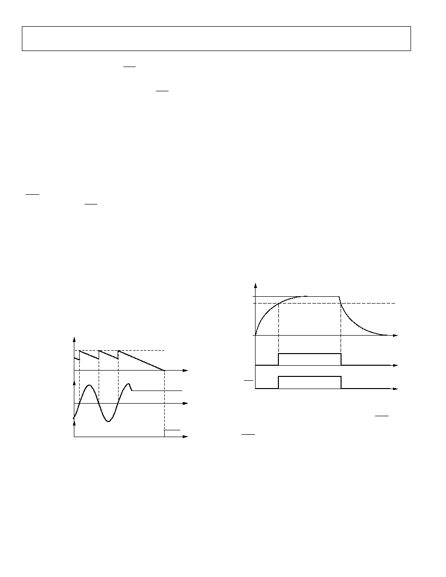
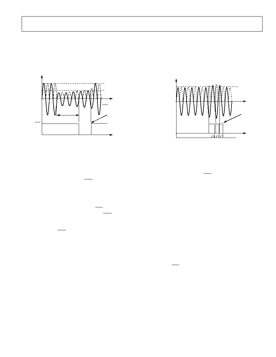
LINE VOLTAGE SAG DETECTION
In addition to detecting the loss of the line voltage when there
are no zero crossings on the voltage channel, the ADE7763 can
also be programmed to detect when the absolute value of the line
voltage drops below a peak value for a specified number of line
cycles. This condition is illustrated in Figure 35.
SAGCYC[7:0] = 0x04
3 LINE CYCLES
SAG RESET HIGH
WHEN CHANNEL 2
EXCEEDS SAGLVL[7:0]
FULL SCALE
SAGLVL[7:0]
SAG
CHANNEL 2
04481-
A-
036
Figure 35. Sag Detection
In Figure 35 the line voltage falls below a threshold that
has been set in the sag level register (SAGLVL[7:0]) for three
line cycles. The quantities 0 and 1 are not valid for the SAGCYC
register, and the contents represent one more than the desired
number of full line cycles. For example, if the DISSAG bit in the
mode register is Logic 0 and the sag cycle register
(SAGCYC[7:0]) contains 0x04, the SAG pin goes active low at
the end of the third line cycle for which the line voltage
(Channel 2 signal) falls below the threshold. As is the case when
zero crossings are no longer detected, the sag event is also
recorded by setting the SAG flag in the interrupt status register.
If the SAG enable bit is set to Logic 1, the IRQ logic output will
go active low--see the Interrupts section. The SAG pin goes
logic high again when the absolute value of the signal on Channel
2 exceeds the level set in the sag level register. This is shown in
Figure 35 when the SAG pin goes high again during the fifth line
cycle from the time when the signal on Channel 2 first dropped
below the threshold level.
Sag Level Set
The contents of the sag level register (1 byte) are compared to
the absolute value of the most significant byte output from
LPF1 after it is shifted left by one bit. For example, the nominal
maximum code from LPF1 with a full-scale signal on Channel 2
is 0x2518--see the Channel 2 Sampling section. Shifting one bit
left gives 0x4A30. Therefore, writing 0x4A to the SAG level
register puts the sag detection level at full scale. Writing 0x00 or
0x01 puts the sag detection level at 0. The SAG level register is
compared to the most significant byte of a waveform sample
after the shift left, and detection occurs when the contents of
the sag level register are greater.
PEAK DETECTION
The ADE7763 can also be programmed to detect when the
absolute value of the voltage or current channel exceeds a
specified peak value. Figure 36 illustrates the behavior of the
peak detection for the voltage channel.
Both Channel 1 and Channel 2 are monitored at the same time.
PKV RESET LOW
WHEN RSTSTATUS
REGISTER IS READ
VPKLVL[7:0]
V
2
READ RSTSTATUS
REGISTER
PKV INTERRUPT
FLAG (BIT 8 OF
STATUS REGISTER)
04481-A
-
037
Figure 36. Peak Level Detection
Figure 36 shows a line voltage exceeding a threshold that has
been set in the voltage peak register (VPKLVL[7:0]). The
voltage peak event is recorded by setting the PKV flag in the
interrupt status register. If the PKV enable bit is set to Logic 1 in
the interrupt mask register, the IRQ logic output will go active
low. Similarly, the current peak event is recorded by setting the
PKI flag in the interrupt status register--see the Interrupts
section.
Peak Level Set
The contents of the VPKLVL and IPKLVL registers are
compared to the absolute value of Channel 1 and Channel 2,
respectively, after they are multiplied by 2. For example, the
nominal maximum code from the Channel 1 ADC with a full-
scale signal is 0x2851EC--see the Channel 1 Sampling section.
Multiplying by 2 gives 0x50A3D8. Therefore, writing 0x50 to
the IPKLVL register, for example, puts the Channel 1 peak
detection level at full scale and sets the current peak detection
to its least sensitive value. Writing 0x00 puts the Channel 1
detection level at 0. Peak level detection is done by comparing
the contents of the IPKLVL register to the incoming Channel 1
sample. The IRQ pin indicates that the peak level is exceeded if
the PKI or PKV bits are set in the interrupt enable register
(IRQEN [15:0]) at Address 0x0A.
Peak Level Record
The ADE7763 records the maximum absolute value reached by
Channel 1 and Channel 2 in two different registers--IPEAK
and VPEAK, respectively. VPEAK and IPEAK are 24-bit,
unsigned registers. These registers are updated each time the
absolute value of the waveform sample from the corresponding
channel is above the value stored in the VPEAK or IPEAK
register. The contents of the VPEAK register correspond to two
ADE7763
Rev. A | Page 18 of 56
times the maximum absolute value observed on the Channel 2
input. The contents of IPEAK represent the maximum absolute
value observed on the Channel 1 input. Reading the RSTVPEAK
and RSTIPEAK registers clears their respective contents after
the read operation.
INTERRUPTS
Interrupts are managed through the interrupt status register
(STATUS[15:0]) and the interrupt enable register
(IRQEN[15:0]). When an interrupt event occurs, the
corresponding flag in the status register is set to Logic 1--see
the Interrupt Status Register section. If the enable bit for this
interrupt in the interrupt enable register is Logic 1, the IRQ
logic output will go active low. The flag bits in the status register
are set irrespective of the state of the enable bits.
To determine the source of the interrupt, the system master
(MCU) should perform a read from the status register with
reset (RSTSTATUS[15:0]). This is achieved by carrying out a
read from Address 0Ch. The IRQ output goes logic high after
the completion of the interrupt status register read command--
see the Interrupt Timing section. When carrying out a read
with reset, the ADE7763 is designed to ensure that no interrupt
events are missed. If an interrupt event occurs as the status
register is being read, the event will not be lost and the IRQ
logic output will be guaranteed to go high for the duration of
the interrupt status register data transfer before going logic low
again to indicate the pending interrupt. See the next section for
a more detailed description.
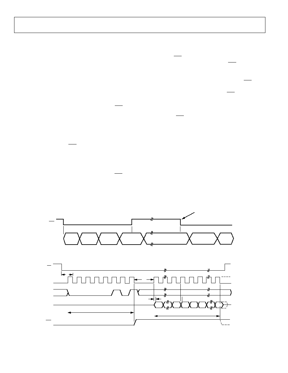
Using Interrupts with an MCU
Figure 38 shows a timing diagram with a suggested imple-
mentation of ADE7763 interrupt management using an MCU.
At time t
1
, the IRQ line goes active low, indicating that one or
more interrupt events have occurred. Tie the IRQ logic output to
a negative edge-triggered external interrupt on the MCU.
Configure the MCU to start executing its interrupt service
routine (ISR) when a negative edge is detected on the IRQ line.
After entering the ISR, disable all interrupts by using the global
interrupt enable bit. At this point, the MCU IRQ external
interrupt flag can be cleared to capture interrupt events that
occur during the current ISR. When the MCU interrupt flag is
cleared, a read from the status register with reset is carried out.
This causes the IRQ line to reset to logic high (t
2
)--see the
Interrupt Timing section. The status register contents are used
to determine the source of the interrupt(s) and, therefore, the
appropriate action to be taken. If a subsequent interrupt event
occurs during the ISR, that event will be recorded by the MCU
external interrupt flag being set again (t
3
). Upon the completion
of the ISR, the global interrupt mask is cleared (same
instruction cycle) and the external interrupt flag causes the
MCU to jump to its ISR again. This ensures that the MCU does
not miss any external interrupts.
IRQ
GLOBAL
INTERRUPT
MASK SET
ISR RETURN
GLOBAL INTERRUPT
MASK RESET
CLEAR MCU
INTERRUPT
FLAG
READ
STATUS WITH
RESET (0x05)
ISR ACTION
(BASED ON STATUS CONTENTS)
MCU
INTERRUPT
FLAG SET
MCU
PROGRAM
SEQUENCE
04481-A
-
038
t
1
t
2
t
3
JUMP
TO
ISR
JUMP
TO
ISR
Figure 37. Interrupt Management
SCLK
DIN
DOUT
IRQ
t
11
t
11
t
9
t
1
READ STATUS REGISTER COMMAND
STATUS REGISTER CONTENTS
DB7
DB7
DB0
CS
0
0
0
0
0
1
0
1
DB0
04481-A
-
039
Figure 38. Interrupt Timing
ADE7763
Rev. A | Page 19 of 56
Interrupt Timing
Review the Serial Interface section before reading this section.
As previously described, when the IRQ output goes low, the
MCU ISR will read the interrupt status register to determine the
source of the interrupt. When reading the status register
contents, the IRQ output is set high upon the last falling edge of
SCLK of the first byte transfer (read interrupt status register
command). The IRQ output is held high until the last bit of the
next 15-bit transfer is shifted out (interrupt status register
contents)--see Figure 37. If an interrupt is pending at this time,
the IRQ output will go low again. If no interrupt is pending, the
IRQ output will stay high.
TEMPERATURE MEASUREMENT
There is an on-chip temperature sensor. A temperature
measurement can be made by setting Bit 5 in the mode register.
When Bit 5 is set logic high in the mode register, the ADE7763
initiates a temperature measurement of the next zero crossing.
When the zero crossing on Channel 2 is detected, the voltage
output from the temperature sensing circuit is connected to
ADC1 (Channel 1) for digitizing. The resulting code is
processed and placed in the temperature register (TEMP[7:0])
approximately 26 µs later (24 CLKIN/4 cycles). If enabled in the
interrupt enable register (Bit 5), the IRQ output will go active
low when the temperature conversion is finished.
The contents of the temperature register are signed (twos
complement) with a resolution of approximately 1.5 LSB/°C.
The temperature register produces a code of 0x00 when the
ambient temperature is approximately -25°C. The temperature
measurement is uncalibrated in the ADE7763 and might have
an offset tolerance as high as ±25°C.
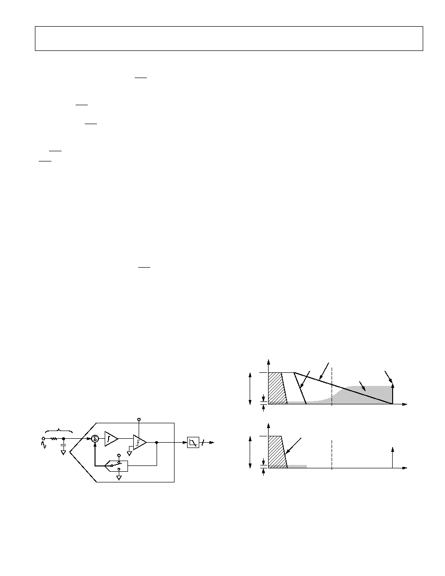
ANALOG-TO-DIGITAL CONVERSION
The analog-to-digital conversion is carried out using two
second-order - ADCs. For simplicity, the block diagram in
Figure 39 shows a first-order - ADC. The converter
comprises two parts: the - modulator and the digital low-
pass filter.
24
DIGITAL
LOW-PASS
FILTER
R
C
ANALOG
LOW-PASS FILTER
+
V
REF
1-BIT DAC
INTEGRATOR
MCLK/4
LATCHED
COMPARATOR
.....10100101.....
+
04481-
A-
040
Figure 39. First-Order
- ADC
A - modulator converts the input signal into a continuous
serial stream of 1s and 0s at a rate determined by the sampling
clock. In the ADE7763, the sampling clock is equal to CLKIN/4.
The 1-bit DAC in the feedback loop is driven by the serial data
stream. The DAC output is subtracted from the input signal. If
the loop gain is high enough, the average value of the DAC
output (and therefore the bit stream) will approach that of the
input signal level. For any given input value in a single sampling
interval, the data from the 1-bit ADC is virtually meaningless.
Only when a large number of samples are averaged can a
meaningful result be obtained. This averaging is carried out in
the second part of the ADC, the digital low-pass filter. By
averaging a large number of bits from the modulator, the low-
pass filter can produce 24-bit data-words that are proportional
to the input signal level.
The - converter uses two techniques to achieve high resolution
from what is essentially a 1-bit conversion technique. The first
is oversampling. Oversampling means that the signal is sampled
at a rate (frequency) that is many times higher than the band-
width of interest. For example, the sampling rate in the ADE7763
is CLKIN/4 (894 kHz) and the band of interest is 40 Hz to 2 kHz.
Oversampling has the effect of spreading the quantization noise
(noise due to sampling) over a wider bandwidth. With the noise
spread more thinly over a wider bandwidth, the quantization
noise in the band of interest decreases--see Figure 40. However,
oversampling alone is not efficient enough to improve the
signal-to-noise ratio (SNR) in the band of interest. For example,
an oversampling ratio of 4 is required just to increase the SNR
by 6 dB (1 bit). To keep the oversampling ratio at a reasonable
level, it is possible to shape the quantization noise so that the
majority of the noise lies at higher frequencies. In the -
modulator, the noise is shaped by the integrator, which has a
high-pass-type response for the quantization noise. The result is
that most of the noise is at higher frequencies, where it can
be removed by the digital low-pass filter. This noise shaping is
shown in Figure 40.
447
0
894
2
NOISE
SIGNAL
DIGITAL
FILTER
ANTIALIAS
FILTER (RC)
SAMPLING
FREQUENCY
HIGH RESOLUTION
OUTPUT FROM DIGITAL
LPF
SHAPED
NOISE
447
0
894
2
NOISE
SIGNAL
FREQUENCY (kHz)
FREQUENCY (kHz)
04481-A
-
041
Figure 40. Noise Reduction due to Oversampling and
Noise Shaping in the Analog Modulator
ADE7763
Rev. A | Page 20 of 56
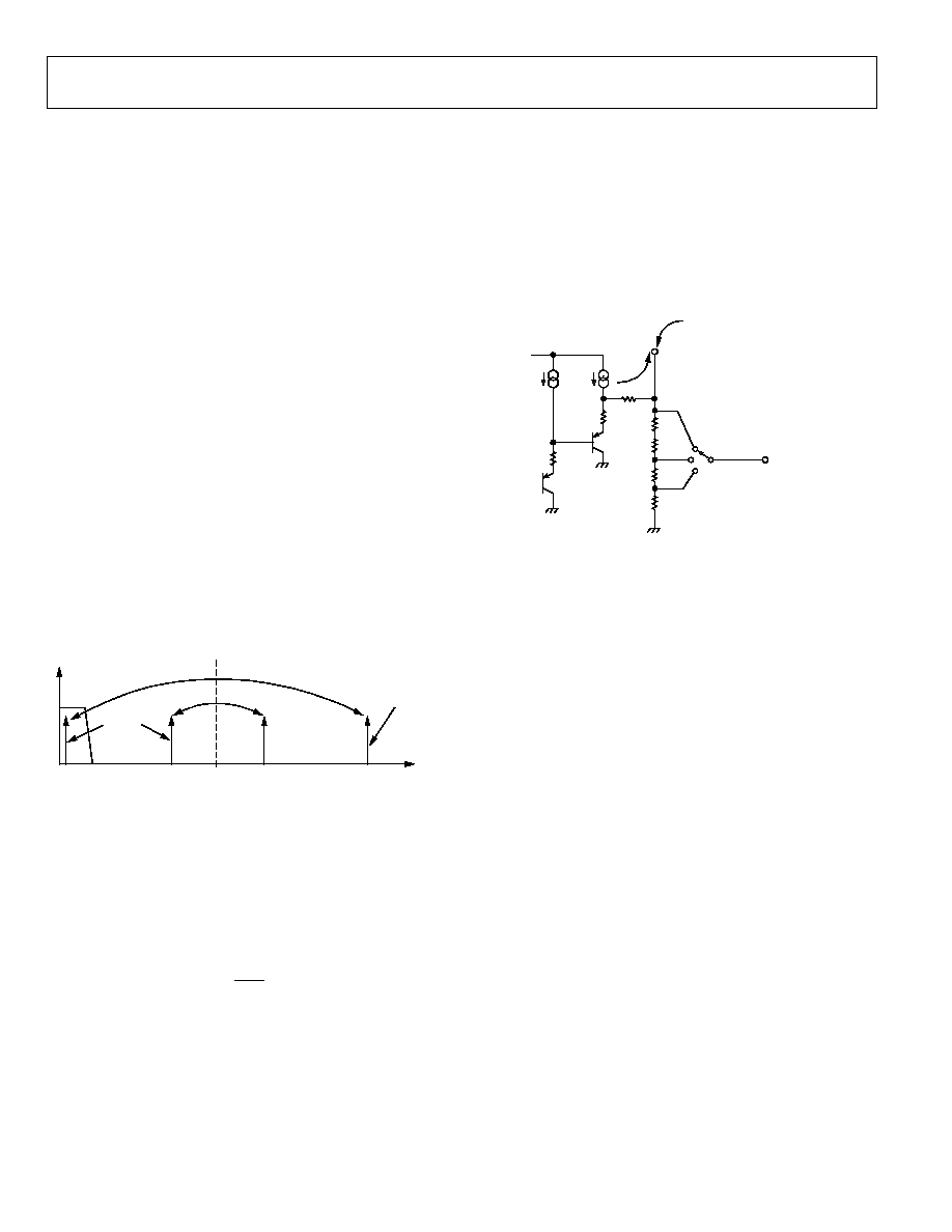
Antialias Filter
Figure 39 also shows an analog low-pass filter (RC) on the input
to the modulator. This filter prevents aliasing, which is an
artifact of all sampled systems. Aliasing means that frequency
components in the input signal to the ADC that are higher than
half the sampling rate of the ADC appear in the sampled signal
at a frequency below half the sampling rate. Figure 41 illustrates
the effect. Frequency components (shown as arrows) above half
the sampling frequency (also known as the Nyquist frequency,
i.e., 447 kHz) are imaged or folded back down below 447 kHz.
This happens with all ADCs, regardless of the architecture. In
the example shown, only frequencies near the sampling
frequency, i.e., 894 kHz, move into the band of interest for
metering, i.e., 40 Hz to 2 kHz. This allows the use of a very
simple LPF (low-pass filter) to attenuate high frequency (near
900 kHz) noise, and it prevents distortion in the band of interest.
For conventional current sensors, a simple RC filter (single-pole
LPF) with a corner frequency of 10 kHz produces an attenuation
of approximately 40 dB at 894 kHz--see Figure 41. The 20 dB
per decade attenuation is usually sufficient to eliminate the effects
of aliasing for conventional current sensors; however, for a di/dt
sensor such as a Rogowski coil, the sensor has a 20 dB per decade
gain. This neutralizes the 20 dB per decade attenuation
produced by one simple LPF. Therefore, when using a di/dt
sensor, care should be taken to offset the 20 dB per decade gain.
One simple approach is to cascade two RC filters to produce the
40 dB per decade attenuation.
SAMPLING
FREQUENCY
IMAGE
FREQUENCIES
ALIASING EFFECTS
0
2
447
894
FREQUENCY (kHz)
04481-
A
-
042
Figure 41. ADC and Signal Processing in Channel 1 Outline Dimensions
ADC Transfer Function
The following expression relates the output of the LPF in the
- ADC to the analog input signal level. Both ADCs in the
ADE7763 are designed to produce the same output code for the
same input signal level.
(
) 3.0492
262,144
IN
OUT
V
Code ADC
V
=
×
×
(1)
Therefore, with a full-scale signal on the input of 0.5 V and an
internal reference of 2.42 V, the ADC output code is nominally
165,151, or 0x2851F. The maximum code from the ADC is
±262,144; this is equivalent to an input signal level of ±0.794 V.
However, for specified performance, do not exceed the 0.5 V
full-scale input signal level.
Reference Circuit
Figure 42 shows a simplified version of the reference output
circuitry. The nominal reference voltage at the REF
IN/OUT
pin is
2.42 V. This is the reference voltage used for the ADCs. However,
Channel 1 has three input range options that are selected by
dividing down the reference value used for the ADC in
Channel 1. The reference value used for Channel 1 is divided
down to ½ and ¼ of the nominal value by using an internal
resistor divider, as shown in Figure 42.
60
µ
A
PTAT
2.5V
1.7k
12.5k
12.5k
12.5k
12.5k
REF
IN/OUT
2.42V
MAXIMUM
LOAD = 10
µ
A
OUTPUT
IMPEDANCE
6k
REFERENCE INPUT
TO ADC CHANNEL 1
(RANGE SELECT)
2.42V, 1.21V, 0.6V
04481-A
-
043
Figure 42. Reference Circuit Output
The REF
IN/OUT
pin can be overdriven by an external source such as
a 2.5 V reference. Note that the nominal reference value supplied
to the ADCs is now 2.5 V, not 2.42 V, which increases the
nominal analog input signal range by 2.5/2.42 × 100% = 3% or
from 0.5 V to 0.5165 V.
The voltage of the ADE7763 reference drifts slightly with changes
in temperature--see Table 1 for the temperature coefficient
specification (in ppm/°C). The value of the temperature drift
varies from part to part. Because the reference is used for the
ADCs in both Channels 1 and 2, any x% drift in the reference
results in 2x% deviation in the meter accuracy. The reference
drift that results from a temperature change is usually very
small, typically much smaller than the drift of other components
on a meter. However, if guaranteed temperature performance is
needed, use an external voltage reference. Alternatively, the
meter can be calibrated at multiple temperatures. Real-time
compensation can be achieved easily by using the on-chip
temperature sensor.
CHANNEL 1 ADC
Figure 43 shows the ADC and signal processing chain for
Channel 1. In waveform sampling mode, the ADC outputs a
signed, twos complement, 24-bit data-word at a maximum of
27.9 kSPS (CLKIN/128). With the specified full-scale analog
input signal of 0.5 V (or 0.25 V or 0.125 V--see the Analog
Inputs section), the ADC produces an output code that is
approximately between 0x28 51EC (+2,642,412d) and
0xD7 AE14 (2,642,412d)--see Figure 43.
ADE7763
Rev. A | Page 21 of 56
×
1,
×
2,
×
4,
×
8,
×
16
ANALOG
INPUT
RANGE
DIGITAL
INTEGRATOR*
HPF
ADC 1
REFERENCE
2.42V, 1.21V, 0.6V
V1
0V
0.5V, 0.25V,
0.125V, 62.5mV,
31.3mV, 15.6mV,
CHANNEL 1
(CURRENT WAVEFORM)
DATA RANGE
ACTIVE AND REACTIVE
POWER CALCULATION
WAVEFORM SAMPLE
REGISTER
CURRENT RMS (IRMS)
CALCULATION
50Hz
V1P
V1N
PGA1
V1
{GAIN[4:3]}
{GAIN[2:0]}
*WHEN DIGITAL INTEGRATOR IS ENABLED, FULL-SCALE OUTPUT DATA IS ATTENUATED
DEPENDING ON THE SIGNAL FREQUENCY BECAUSE THE INTEGRATOR HAS A 20dB/DECADE
FREQUENCY RESPONSE. WHEN DISABLED, THE OUTPUT IS NOT ATTENUATED FURTHER.
ADC OUTPUT
WORD RANGE
0xD 7AE4
0x0 0000
0x28 51EC
0xD 7AE4
0x00 0000
0x28 51EC
CHANNEL 1
(CURRENT WAVEFORM)
DATA RANGE AFTER
INTEGRATOR (50Hz)
0xEI 08C4
0x00 0000
0x1E F73C
60Hz
CHANNEL 1
(CURRENT WAVEFORM)
DATA RANGE AFTER
INTEGRATOR (60Hz)
0xE6 31F8
0x00 0000
0x19 CE08
04481-A
-
044
dt
Figure 43. ADC and Signal Processing in Channel 1
Channel 1 Sampling
The waveform samples may be routed to the waveform register
(MODE[14:13] = 1, 0) for the system master (MCU) to read. In
waveform sampling mode, set the WSMP bit (Bit 3) in the
interrupt enable register to Logic 1. The active and apparent
power as well as the energy calculation remain uninterrupted
during waveform sampling.
In waveform sampling mode, choose one of four output sample
rates using Bits 11 and 12 of the mode register (WAVSEL 1, 0).
The output sample rate can be 27.9 kSPS, 14 kSPS, 7 kSPS, or
3.5 kSPS--see the Mode Register (0X09) section. The interrupt
request output, IRQ, signals a new sample availability by going
active low. The timing is shown in Figure 44. The 24-bit wave-
form samples are transferred from the ADE7763 one byte (eight
bits) at a time, with the most significant byte shifted out first.
The 24-bit data-word is right justified--see the Serial Interface
section. The interrupt request output IRQ stays low until the
interrupt routine reads the reset status register--see the
Interrupts section.
CHANNEL 1 DATA
(24 BITS)
READ FROM WAVEFORM
SIGN
0
IRQ
SCLK
DIN
DOUT
0 0 01 HEX
04481-A
-
045
Figure 44. Waveform Sampling Channel 1
Channel 1 RMS Calculation
The root mean square (rms) value of a continuous signal V(t) is
defined as
VRMS =
×
T
dt
t
V
T
0
2
)
(
1
(2)
For time sampling signals, the rms calculation involves squaring
the signal, taking the average, and obtaining the square root:
VRMS =
=
×
N
i
i
V
N
1
2
)
(
1
(3)
The ADE7763 simultaneously calculates the rms values for
Channel 1 and Channel 2 in different registers. Figure 45 shows
the detail of the signal processing chain for the rms calculation
on Channel 1. The Channel 1 rms value is processed from the
samples used in the Channel 1 waveform sampling mode. The
Channel 1 rms value is stored in an unsigned, 24-bit register
(IRMS). One LSB of the Channel 1 rms register is equivalent to
1 LSB of a Channel 1 waveform sample. The update rate of the
Channel 1 rms measurement is CLKIN/4.
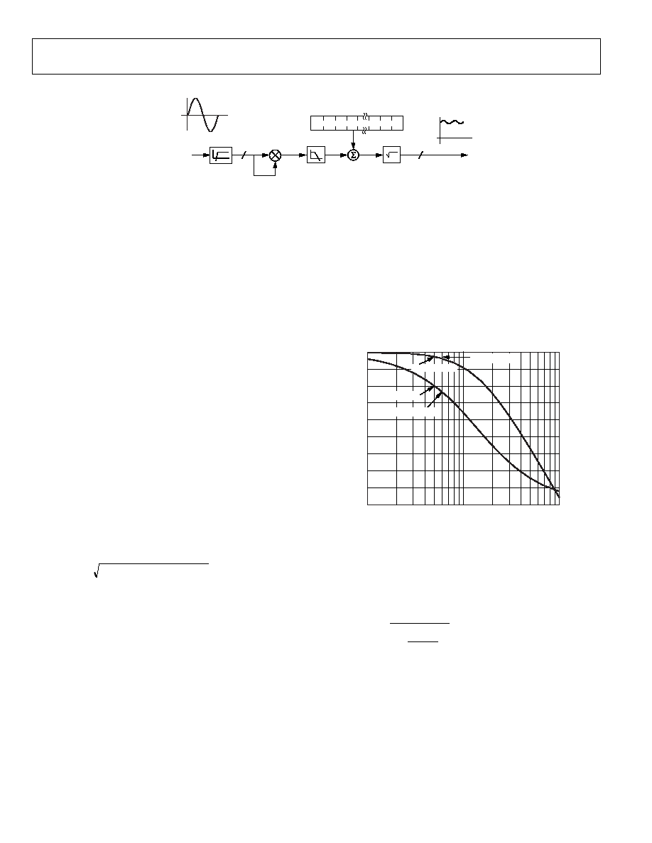
ADE7763
Rev. A | Page 22 of 56
IRMS(t)
LPF3
HPF1
CHANNEL 1
0x1C 82B3
0x00
+
IRMSOS[11:0]
IRMS
CURRENT SIGNAL (i(t))
2
26
2
25
sgn
2
27
2
17
2
16
2
15
04481-A
-046
0x28 51EC
0x00
0xD7 AE14
24
24
Figure 45. Channel 1 RMS Signal Processing
With the specified full-scale analog input signal of 0.5 V, the ADC
produces an output code that is approximately ±2,642,412d--
see the Channel 1 ADC section. The equivalent rms value of a
full-scale ac signal is 1,868,467d (0x1C82B3). The current rms
measurement provided in the ADE7763 is accurate to within
1% for signal input between full scale and full scale/100.
Converting the register value to its equivalent in amps must be
done externally in the microprocessor using an amps/LSB
constant. To minimize noise, synchronize the reading of the
rms register with the zero crossing of the voltage input and take
the average of a number of readings.
Channel 1 RMS Offset Compensation
The ADE7763 incorporates a Channel 1 rms offset compensa-
tion register (IRMSOS). This is a 12-bit, signed register that can
be used to remove offset in the Channel 1 rms calculation. An
offset might exist in the rms calculation due to input noises that
are integrated in the dc component of V
2
(t). The offset calibration
allows the content of the IRMS register to be maintained at 0
when no input is present on Channel 1.
One LSB of the Channel 1 rms offset is equivalent to 32,768 LSB
of the square of the Channel 1 rms register. Assuming that the
maximum value from the Channel 1 rms calculation is
1,868,467d with full-scale ac inputs, then 1 LSB of the Channel 1
rms offset represents 0.46% of the measurement error at 60 dB
down of full scale.
IRMS =
32768
2
×
+ IRMSOS
IRMS
0
(4)
where
IRMS
0
is the rms measurement without offset correction.
To measure the offset of the rms measurement, two data points
are needed from nonzero input values, for example, the base
current, I
b
, and I
max
/100. The offset can be calculated from these
measurements.
CHANNEL 2 ADC
Channel 2 Sampling
In Channel 2 waveform sampling mode (MODE[14:13] = 1, 1
and WSMP = 1), the ADC output code scaling for Channel 2 is
not the same as it is for Channel 1. The Channel 2 waveform
sample is a 16-bit word and sign extended to 24 bits. For normal
operation, the differential voltage signal between V2P and V2N
should not exceed 0.5 V. With maximum voltage input (±0.5 V
at PGA gain of 1), the output from the ADC swings between
0x2852 and 0xD7AE (±10,322d). However, before being passed
to the waveform register, the ADC output is passed through a
single-pole, low-pass filter with a cutoff frequency of 140 Hz.
The plots in Figure 46 show the magnitude and phase response
of this filter.
FREQUENCY (Hz)
0
10
1
10
2
10
3
PH
A
SE (
D
egrees)
20
10
40
50
60
30
70
80
90
0
18
GAIN (
d
B)
60Hz,
0.73dB
50Hz,
0.52dB
60Hz,
23.2°
50Hz,
19.7°
8
10
14
12
16
2
4
6
04481-A
-
047
Figure 46. Magnitude and Phase Response of LPF1
The LPF1 has the effect of attenuating the signal. For example,
if the line frequency is 60 Hz, the signal at the output of LPF1
will be attenuated by about 8%.
|
H(f)| =
2
Hz
140
Hz
60
1
1
+
= 0.919 = -0.73 db
(5)
Note LPF1 does not affect the active power calculation. The
signal processing chain in Channel 2 is illustrated in Figure 47.
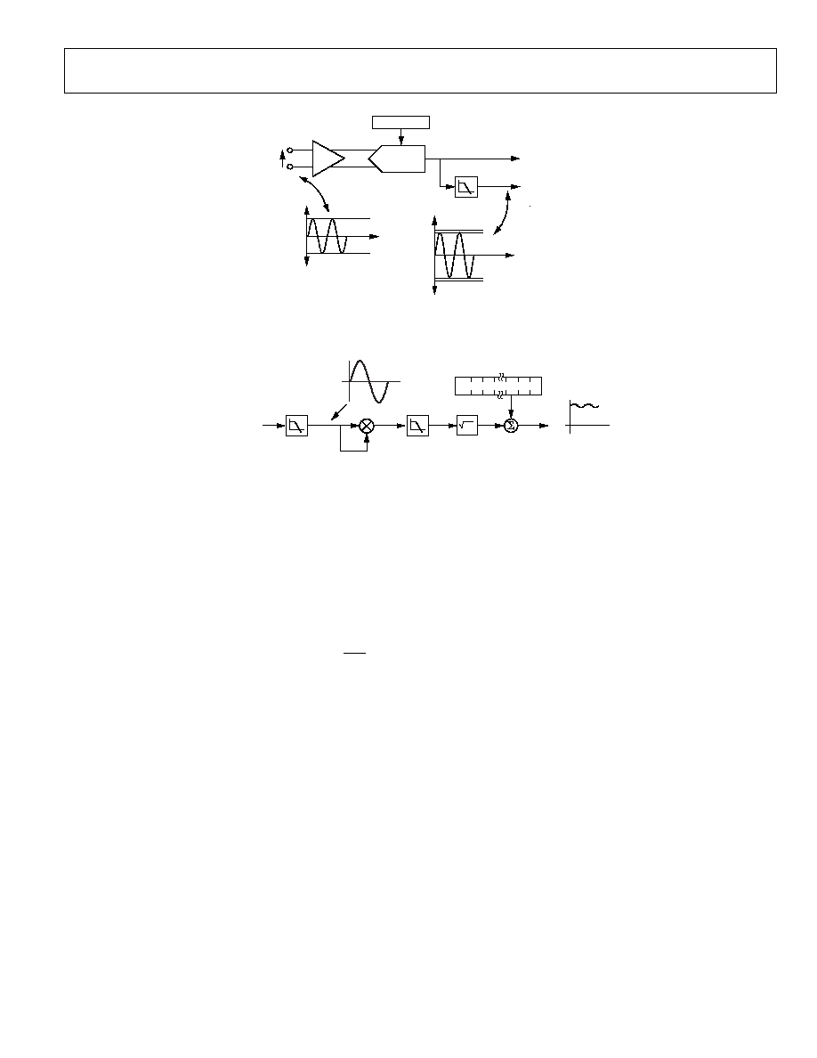
ADE7763
Rev. A | Page 23 of 56
V1
ADC 2
0V
ANALOG
INPUT RANGE
0.5V, 0.25V, 0.125V,
62.5mV, 31.25mV
REFERENCE
LPF1
ACTIVE AND REACTIVE
ENERGY CALCULATION
VRMS CALCULATION
AND WAVEFORM
SAMPLING
(PEAK/SAG/ZX)
PGA2
×
1,
×
2,
×
4,
×
8,
×
16
{GAIN[7:5]}
V2P
V2N
V2
2.42V
0x2852
0x2581
0xDAE8
0xD7AE
0x0000
LPF OUTPUT
WORD RANGE
04481-A
-
048
Figure 47. ADC and Signal Processing in Channel 2
VRMS[23:0]
LPF3
LPF1
CHANNEL 2
0x17D338
0x00
+
+
VRMOS[11:0]
VOLTAGE SIGNAL (V(t))
2
9
sgn
2
8
2
2
2
1
2
0
04481-A
-
049
0x2518
0x0
0xDAE8
Figure 48. Channel 2 RMS Signal Processing
Channel 2 has only one analog input range (0.5 V differential).
Like Channel 1, Channel 2 has a PGA with gain selections of 1,
2, 4, 8, and 16. For energy measurement, the output of the ADC
is passed directly to the multiplier and is not filtered. An HPF is
not required to remove any dc offset; it is only required that the
offset is removed from one channel to eliminate errors caused
by offsets in the power calculation. In waveform sampling mode,
one of four output sample rates can be chosen by using Bits 11
and 12 of the mode register. The available output sample rates
are 27.9 kSPS, 14 kSPS, 7 kSPS, or 3.5 kSPS--see the Mode
Register (0X09) section. The interrupt request output IRQ
indicates that a sample is available by going active low. The
timing is the same as that for Channel 1, as shown in Figure 44.
Channel 2 RMS Calculation
Figure 48 shows the details of the signal processing chain for the
rms calculation on Channel 2. The Channel 2 rms value is
processed from the samples used in the Channel 2 waveform
sampling mode. The rms value is slightly attenuated due to
LPF1. The Channel 2 rms value is stored in the unsigned, 24-bit
VRMS register. The update rate of the Channel 2 rms
measurement is CLKIN/4.
With the specified full-scale ac analog input signal of 0.5 V, the
output from LPF1 swings between 0x2518 and 0xDAE8 at
60 Hz--see the Channel 2 ADC section. The equivalent rms
value of this full-scale ac signal is approximately 1,561,400
(0x17 D338) in the VRMS register. The voltage rms measure-
ment provided in the ADE7763 is accurate to within ±0.5% for
signal input between full scale and full scale/20. The conversion
from the register value to volts must be done externally in the
microprocessor using a volts/LSB constant. Because the low-pass
filter used for calculating the rms value is imperfect, there is some
ripple noise from 2 term present in the rms measurement. To
minimize the effect of noise in the reading, synchronize the rms
reading with the zero crossings of the voltage input.
Channel 2 RMS Offset Compensation
The ADE7763 incorporates a Channel 2 rms offset
compensation register (VRMSOS). This is a 12-bit, signed
register that can be used to remove offset in the Channel 2 rms
calculation. An offset could exist in the rms calculation due to
input noises and dc offset in the input samples. The offset
calibration allows the contents of the VRMS register to be
maintained at 0 when no voltage is applied. One LSB of the
Channel 2 rms offset is equivalent to 1 LSB of the rms register.
Assuming that the maximum value of the Channel 2 rms
calculation is 1,561,400d with full-scale ac inputs, then 1 LSB of
the Channel 2 rms offset represents 0.064% of measurement
error at 60 dB down of full scale.
VRMS = VRMS
0
+
VRMSOS (6)
where
VRMS
0
is the rms measurement without offset
correction.
The voltage rms offset compensation should be done by testing
the rms results at two nonzero input levels. One measurement
can be done close to full scale and the other at approximately
full scale/10. The voltage offset compensation can be derived
from these measurements. If the voltage rms offset register does
not have enough range, the CH2OS register can also be used.

ADE7763
Rev. A | Page 24 of 56
PHASE COMPENSATION
When the HPF is disabled, the phase error between Channel 1
and Channel 2 is 0 from dc to 3.5 kHz. When HPF is enabled,
Channel 1 has the phase response illustrated in Figure 50 and
Figure 51. Figure 52 shows the magnitude response of the filter.
As seen from the plots, the phase response is almost 0 from
45 Hz to 1 kHz, which is all that is required in typical energy
measurement applications. However, despite being internally
phase-compensated, the ADE7763 must work with transducers,
which could have inherent phase errors. For example, a phase
error of 0.1° to 0.3° is not uncommon for a current transformer
(CT). Phase errors can vary from part to part and must be
corrected in order to perform accurate power calculations. The
errors associated with phase mismatch are particularly
noticeable at low power factors. The ADE7763 provides a
means of digitally calibrating these small phase errors by
allowing a short time delay or time advance to be introduced
into the signal processing chain to compensate for these errors.
Because the compensation is in time, this technique should only
be used for small phase errors in the range of 0.1° to 0.5°.
Correcting large phase errors using a time shift technique can
introduce significant phase errors at higher harmonics.
The phase calibration register (PHCAL[5:0]) is a twos comple-
ment, signed, single-byte register that has values ranging from
0x21 (31d) to 0x1F (+31d).
The register is centered at 0Dh, so that writing 0Dh to the register
produces 0 delay. By changing the PHCAL register, the time
delay in the Channel 2 signal path can change from 102.12 µs
to +39.96 µs (CLKIN = 3.579545 MHz). One LSB is equivalent
to 2.22 µs (CLKIN/8) time delay or advance. A line frequency of
60 Hz gives a phase resolution of 0.048° at the fundamental (i.e.,
360° × 2.22 µs × 60 Hz). Figure 49 illustrates how the phase
compensation is used to remove a 0.1° phase lead in Channel 1
due to the external transducer. To cancel the lead (0.1°) in
Channel 1, a phase lead must also be introduced into Channel 2.
The resolution of the phase adjustment allows the introduction
of a phase lead in increments of 0.048°. The phase lead is
achieved by introducing a time advance in Channel 2. A time
advance of 4.44 µs is made by writing -2 (0x0B) to the time delay
block, thus reducing the amount of time delay by 4.44 µs, or
equivalently, a phase lead of approximately 0.1° at line frequency
of 60 Hz. 0x0B represents 2 because the register is centered
with 0 at 0Dh.
1
1
0
1
0
0
1
5
0
PGA1
V1P
V1N
V1
ADC 1
HPF
24
PGA2
V2P
V2N
V2
ADC 2
DELAY BLOCK
2.22
µ
s/LSB
24
LPF2
V2
V1
60Hz
0.1°
V1
V2
CHANNEL 2 DELAY
REDUCED BY 4.44
µ
s
(0.1°LEAD AT 60Hz)
0x0B IN PHCAL [5.0]
PHCAL[5:0]
102.12
µ
s TO +39.96
µ
s
60Hz
04481-
A-
050
Figure 49. Phase Calibration
FREQUENCY (Hz)
PH
A
SE (
D
egrees)
0.9
0.8
0.7
0.6
0.5
0.4
0.3
0.2
0.1
0
0.1
10
2
10
3
10
4
04481-A
-
051
Figure 50. Combined Phase Response of HPF and
Phase Compensation (10 Hz to 1 kHz)
FREQUENCY (Hz)
0.20
40
PH
A
SE (
D
egrees)
0.18
0.16
0.14
0.12
0.10
0.08
0
0.02
0.04
0.06
45
50
55
60
65
70
04481-A
-
052
Figure 51. Combined Phase Response of HPF and
Phase Compensation (40 Hz to 70 Hz)
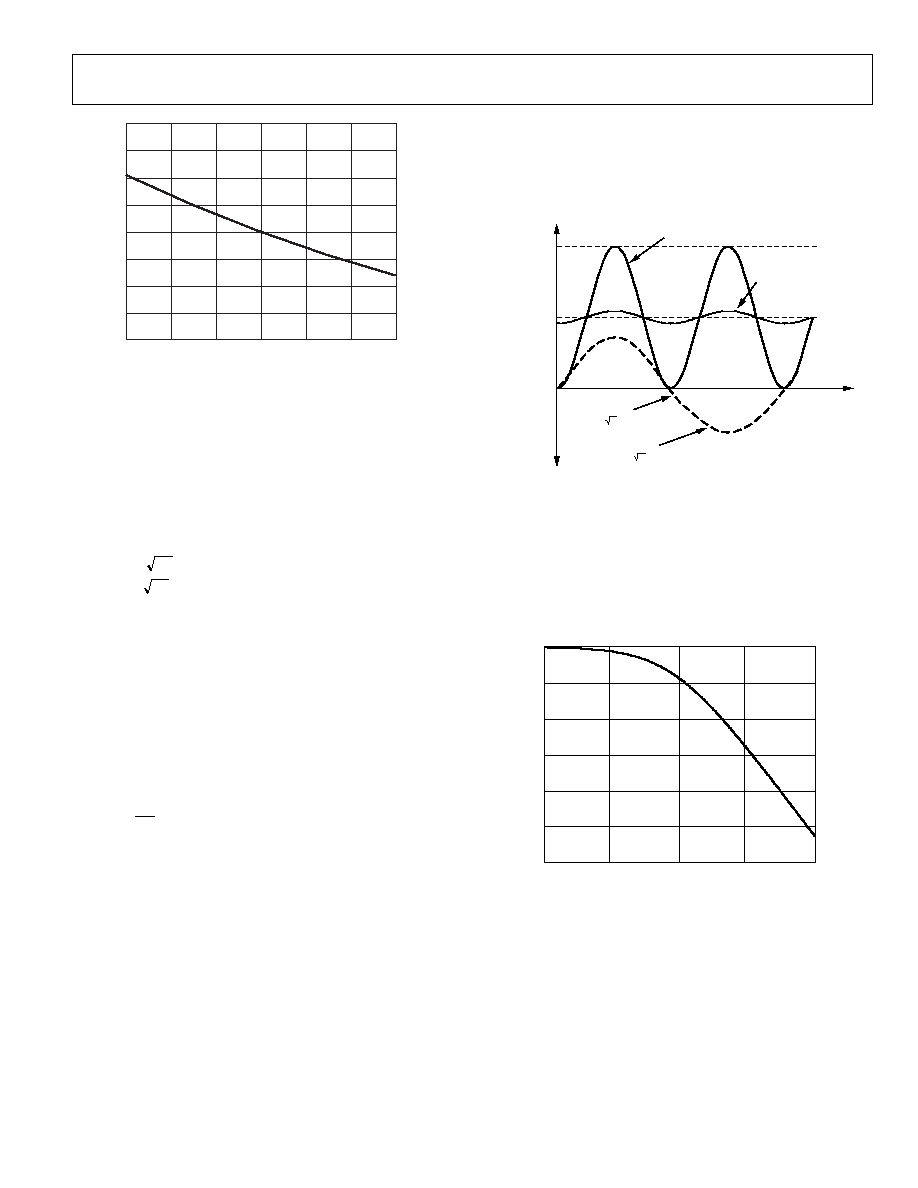
ADE7763
Rev. A | Page 25 of 56
FREQUENCY (Hz)
0.4
ER
R
O
R
(
%
)
54
56
58
60
62
64
66
0.3
0.2
0.1
0.0
0.1
0.2
0.3
0.4
04481-A
-
053
Figure 52. Combined Gain Response of HPF and Phase Compensation
ACTIVE POWER CALCULATION
Power is defined as the rate of energy flow from the source to
the load. It is defined as the product of the voltage and current
waveforms. The resulting waveform is called the instantaneous
power signal and is equal to the rate of energy flow at any given
time. The unit of power is the watt or joules/s. Equation 9 gives
an expression for the instantaneous power signal in an ac system.
)
sin(
2
)
(
t
V
t
v
×
=
(7)
)
sin(
2
)
(
t
I
t
i
×
=
(8)
where:
V is the rms voltage.
I is the rms current.
)
(
)
(
)
(
t
i
t
v
t
p
×
=
)
2
cos(
)
(
t
VI
VI
t
p
-
=
(9)
The average power over an integral number of line cycles (n) is
given by the expression in Equation 10.
=
=
nT
VI
dt
t
p
nT
P
0
)
(
1
(10)
where:
T is the line cycle period.
P is the active or real power.
Note that the active power is equal to the dc component of the
instantaneous power signal
p(t) in Equation 8, i.e., VI. This is
the relationship used to calculate active power in the ADE7763.
The instantaneous power signal
p(t) is generated by multiplying
the current and voltage signals. The dc component of the instan-
taneous power signal is then extracted by LPF2 (low-pass filter)
to obtain the active power information. This process is illustrated
in Figure 53.
INSTANTANEOUS
POWER SIGNAL
p(t) = v
×
i-v
×
i
×
cos(2
t)
ACTIVE REAL POWER
SIGNAL = v
×
i
0x19 999A
VI
0xC CCCD
0x0 0000
04481-A
-
054
CURRENT
i(t) = 2
×
i
×
sin(
t)
VOLTAGE
v(t) = 2
×
v
×
sin(
t)
Figure 53. Active Power Calculation
Because LPF2 does not have an ideal "brick wall" frequency
response (see Figure 54), the active power signal has some
ripple due to the instantaneous power signal. This ripple is
sinusoidal and has a frequency equal to twice the line frequency.
Because the ripple is sinusoidal in nature, it is removed when the
active power signal is integrated to calculate energy--see the
Energy Calculation section.
FREQUENCY (Hz)
24
1
dB
20
3
10
30
100
12
16
8
4
0
04481-A
-
055
Figure 54. Frequency Response of LPF2
ADE7763
Rev. A | Page 26 of 56
APOS[15:0]
WGAIN[11:0]
WDIV[7:0]
LPF2
CURRENT
CHANNEL
VOLTAGE
CHANNEL
OUTPUT LPF2
TIME (nT)
4
CLKIN
T
ACTIVE POWER
SIGNAL
+
+
AENERGY[23:0]
OUTPUTS FROM THE LPF2 ARE
ACCUMULATED (INTEGRATED) IN
THE INTERNAL ACTIVE ENERGY REGISTER
UPPER 24 BITS ARE
ACCESSIBLE THROUGH
AENERGY[23:0] REGISTER
23
0
48
0
WAVEFORM
REGISTER
VALUES
04481-A
-
056
%
Figure 55. Active Energy Calculation
Figure 55 shows the signal processing chain for the active power
calculation. The active power is calculated by low-pass filtering
the instantaneous power signal. Note that when reading the
waveform samples from the output of LPF2, the gain of the
active energy can be adjusted by using the multiplier and watt
gain register (WGAIN[11:0]). The gain is adjusted by writing a
twos complement 12-bit word to the watt gain register.
Equation 11 shows how the gain adjustment is related to the
contents of the watt gain register:
+
×
=
12
2
1
WGAIN
Power
Active
WGAIN
Output
(11)
For example, when 0x7FF is written to the watt gain register, the
power output is scaled up by 50%. 0x7FF = 2047d, 2047/2
12
= 0.5.
Similarly, 0x800 = 2048d (signed twos complement) and
power output is scaled by 50%. Each LSB scales the power
output by 0.0244%. Figure 56 shows the maximum code
(hexadecimal) output range for the active power signal (LPF2).
Note that the output range changes depending on the contents
of the watt gain register. The minimum output range is given
when the watt gain register contents are equal to 0x800, and the
maximum range is given by writing 0x7FF to the watt gain
register. This can be used to calibrate the active power (or
energy) calculation.
0x1 3333
0xCCCD
0x6666
0xF 999A
0xF 3333
0xE CCCD
0x0 0000
ACTIV
E
P
O
WE
R OUTP
UT
POSITIVE
POWER
NEGATIVE
POWER
0x000
0x7FF
0x800
{WGAIN[11:0]}
ACTIVE POWER
CALIBRATION RANGE
04481-A
-
057
Figure 56. Active Power Calculation Output Range
ENERGY CALCULATION
As stated earlier, power is defined as the rate of energy flow.
This relationship is expressed mathematically in Equation 12.
dt
dE
P
=
(12)
where:
P is power.
E is energy.
Conversely, energy is given as the integral of power.
= Pdt
E
(13)

ADE7763
Rev. A | Page 27 of 56
FOR WAVEFORM
ACCUMULATION
1
24
24
LPF2
V
I
0x1 9999
0x19 999A
0x00 0000
INSTANTANEOUS
POWER SIGNAL p(t)
FOR WAVEF0RM
SAMPLING
32
0xC CCCD
CURRENT SIGNAL i(t)
HPF
VOLTAGE SIGNAL v(t)
MULTIPLIER
+
+
APOS[15:0]
2
6
sgn
2
5
2
-6
2
-7
2
-8
04481-A
-
058
WGAIN[11:0]
Figure 57. Active Power Signal Processing
The ADE7763 achieves the integration of the active power
signal by continuously accumulating the active power signal in
an internal unreadable 49-bit energy register. The active energy
register (AENERGY[23:0]) represents the upper 24 bits of this
internal register. This discrete time accumulation or summation
is equivalent to integration in continuous time. Equation 14
expresses this relationship.
0
1
( )
(
)
t
n
E
p t dt Lim
p nT
T
=
=
=
×
(14)
where:
n is the discrete time sample number.
T is the sample period.
The discrete time sample period (
T) for the accumulation
register is 1.1 µs (4/CLKIN). In addition to calculating the
energy, this integration removes any sinusoidal components
that might be in the active power signal.
Figure 57 shows this discrete time integration, or accumulation.
The active power signal in the waveform register is continuously
added to the internal active energy register. This addition is a
signed addition; therefore, negative energy is subtracted from
the active energy contents. The exception to this is when POAM
is selected in the MODE[15:0] register, in which case only
positive energy contributes to the active energy accumulation--
see the Positive-Only Accumulation Mode section.
The output of the multiplier is divided by WDIV. If the value in
the WDIV register is equal to 0, then the internal active energy
register is divided by 1. WDIV is an 8-bit, unsigned register.
After dividing by WDIV, the active energy is accumulated in a
49-bit internal energy accumulation register. The upper 24 bits
of this register are accessible through a read to the active energy
register (AENERGY[23:0]). A read to the RAENERGY register
returns the content of the AENERGY register, and the upper
24 bits of the internal register are cleared. As shown in Figure 57,
the active power signal is accumulated in an internal 49-bit,
signed register. The active power signal can be read from the
waveform register by setting MODE[14:13] = 0, 0 and setting
the WSMP bit (Bit 3) in the interrupt enable register to 1. Like
Channel 1 and Channel 2 waveform sampling modes, the
waveform data is available at sample rates of 27.9 kSPS, 14 kSPS,
7 kSPS, or 3.5 kSPS--see Figure 44.
Figure 58 shows this energy accumulation for full-scale signals
(sinusoidal) on the analog inputs. The three curves illustrate the
minimum time for the energy register to roll over when the active
power gain register contents are 0x7FF, 0x000, and 0x800. The
watt gain register is used to carry out power calibration. As
shown, the fastest integration time occurs when the watt gain
register is set to maximum full scale, i.e., 0x7FF.
0x00 0000
0x7F FFFF
0x3F FFFF
0x40 0000
0x80 0000
AENERGY[23:0]
6.2
4
8
12.5
TIME (minutes)
WGAIN = 0x7FF
WGAIN = 0x000
WGAIN = 0x800
04481-A
-
059
Figure 58. Energy Register Rollover Time for Full-Scale Power
(Minimum and Maximum Power Gain)
Note that the energy register contents roll over to full-scale
negative (0x80 0000) and continue increasing in value when the
power or energy flow is positive--see Figure 58. Conversely, if
the power was negative, the energy register would underflow to
full-scale positive (0x7F FFFF) and continue decreasing in
value.
By using the interrupt enable register, the ADE7763 can be
configured to issue an interrupt (IRQ) when the active energy
register is more than half full (positive or negative), or when an
overflow or underflow occurs.

ADE7763
Rev. A | Page 28 of 56
Integration Time under Steady Load
As mentioned in the last section, the discrete time sample
period (
T) for the accumulation register is 1.1 µs (4/CLKIN).
With full-scale sinusoidal signals on the analog inputs and the
WGAIN register set to 0x000, the average word value from each
LPF2 is 0xC CCCD--see Figure 53. The maximum positive
value that can be stored in the internal 49-bit register before it
overflows is 2
48
, or 0xFFFF FFFF FFFF. The integration time
under these conditions with WDIV = 0 is calculated as follows:
Time =
min
26
.
6
s
8
.
375
s
12
.
1
CCCD
0xC
FFFF
FFFF
0xFFFF
=
=
µ
×
(15)
When WDIV is set to a value other than 0, the integration time
varies, as shown in Equation 16.
Time
= Time
WDIV = 0
× WDIV (16)
POWER OFFSET CALIBRATION
The ADE7763 incorporates an active power offset register
(APOS[15:0]). This is a signed, twos complement, 16-bit
register that can be used to remove offsets in the active power
calculation--see Figure 57. An offset could exist in the power
calculation due to crosstalk between channels on the PCB or in
the IC itself. The offset calibration allows the contents of the
active power register to be maintained at 0 when no power is
being consumed.
The 256 LSBs (APOS = 0x0100) written to the active power
offset register are equivalent to 1 LSB in the waveform sample
register. Assuming the average value output from LPF2 is
0xC CCCD (838,861d) when inputs on Channels 1 and 2 are
both at full scale. At -60 dB down on Channel 1 (1/1000 of the
Channel 1 full-scale input), the average word value output from
LPF2 is 838.861 (838,861/1,000). One LSB in the LPF2 output
has a measurement error of 1/838.861 × 100% = 0.119% of the
average value. The active power offset register has a resolution
equal to 1/256 LSB of the waveform register; therefore, the
power offset correction resolution is 0.00047%/LSB
(0.119%/256) at 60 dB.
ENERGY-TO-FREQUENCY CONVERSION
The ADE7763 provides energy-to-frequency conversion for
calibration purposes. After initial calibration at manufacturing,
the manufacturer or end customer often verifies the energy meter
calibration. One convenient way to verify the meter calibration
is for the manufacturer to provide an output frequency, which is
proportional to the energy or active power under steady load
conditions. This output frequency can provide a simple, single-
wire, optically isolated interface to external calibration equip-
ment. Figure 59 illustrates the energy-to-frequency conversion.
CFNUM[11:0]
CF
11
0
CFDEN[11:0]
11
0
AENERGY[48:0]
48
0
04481-A
-
060
%
DFC
Figure 59. Energy-to-Frequency Conversion
A digital-to-frequency converter (DFC) is used to generate the
CF pulsed output. The DFC generates a pulse each time 1 LSB
in the active energy register is accumulated. An output pulse is
generated when (CFDEN + 1)/(CFNUM + 1) number of pulses
are generated at the DFC output. Under steady load conditions,
the output frequency is proportional to the active power.
The maximum output frequency, with ac input signals at full
scale, CFNUM = 0x00, and CFDEN = 0x00, is approximately
23 kHz.
There are two unsigned, 12-bit registers, CFNUM[11:0] and
CFDEN[11:0], that can be used to set the CF frequency to a wide
range of values. These frequency-scaling registers are 12-bit
registers that can scale the output frequency by 1/2
12
to 1 with a
step of 1/2
12
.
If the value 0 is written to any of these registers, the value 1 will
be applied to the register. The ratio (CFNUM + 1)/(CFDEN + 1)
should be smaller than 1 to ensure proper operation. If the ratio
of the registers (CFNUM + 1)/(CFDEN + 1) is greater than 1, the
register values will be adjusted to a ratio (CFNUM + 1)/
(CFDEN + 1) of 1. For example, if the output frequency is
1.562 kHz while the contents of CFDEN are 0 (0x000), then the
output frequency can be set to 6.1 Hz by writing 0xFF to the
CFDEN register.
When CFNUM and CFDEN are both set to one, the CF pulse
width is fixed at 16 CLKIN/4 clock cycles, approximately 18 µs
with a CLKIN of 3.579545 MHz. If the CF pulse output is longer
than 180 ms for an active energy frequency of less than 5.56 Hz,
the pulse width is fixed at 90 ms. Otherwise, the pulse width is
50% of the duty cycle.
The output frequency has a slight ripple at a frequency equal to
twice the line frequency. This is due to imperfect filtering of the
instantaneous power signal to generate the active power signal--
see the Active Power Calculation section. Equation 8 gives an
expression for the instantaneous power signal. This is filtered by
LPF2, which has a magnitude response given by Equation 17.
2
9
.
8
1
1
)
(
2
f
f
H
+
=
(17)
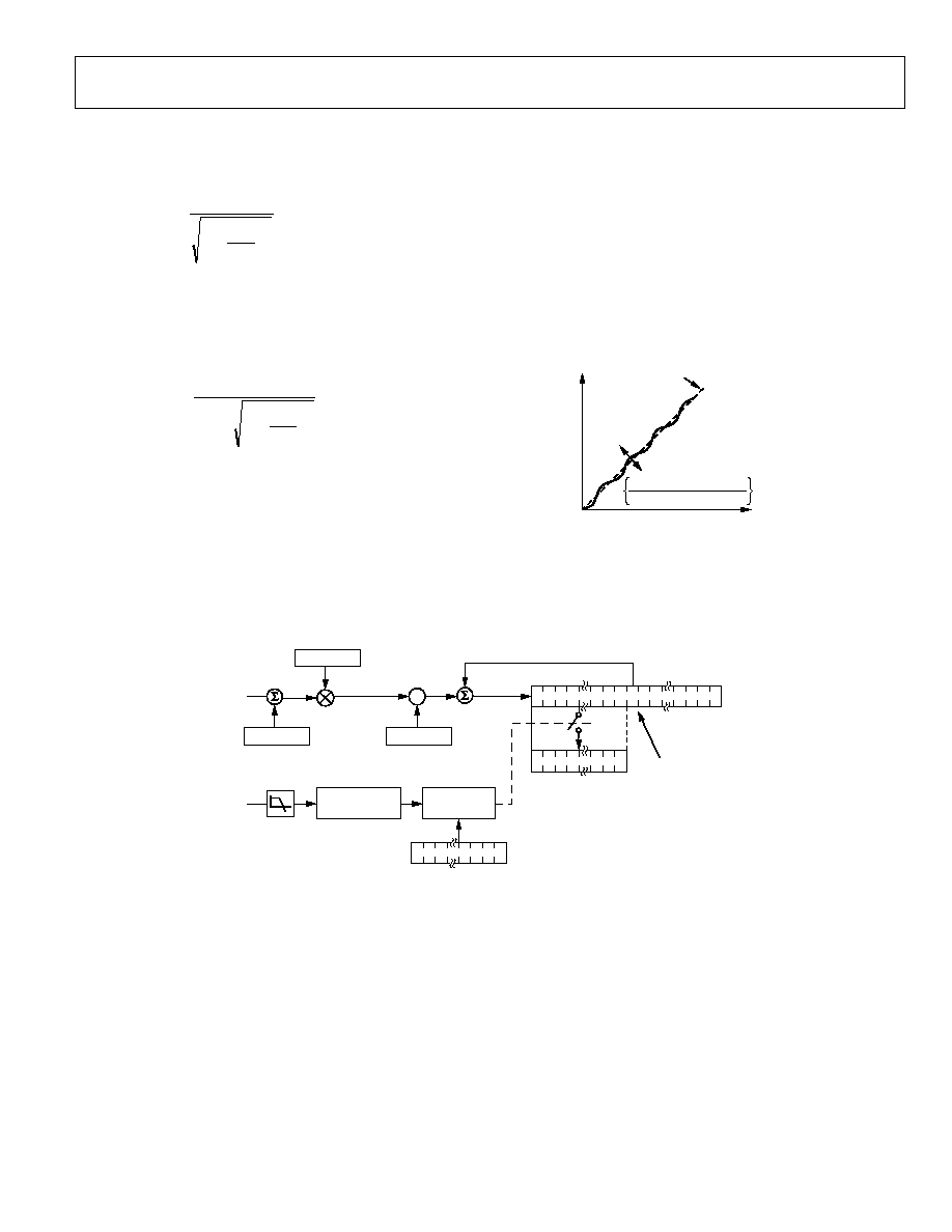
ADE7763
Rev. A | Page 29 of 56
The active power signal (output of LPF2) can be rewritten as
)
4
cos(
9
.
8
2
1
)
(
2
t
f
f
VI
VI
t
p
L
L
×
+
-
=
(18)
where f
L
is the line frequency, for example, 60 Hz.
From Equation 13,
)
4
sin(
9
.
8
2
1
4
)
(
2
t
f
f
f
VI
VIt
t
E
L
L
L
×
+
-
=
(19)
Note that in Equation 19 there is a small ripple in the energy
calculation due to a sin(2t) component. This is shown graphi-
cally in Figure 60. The active energy calculation is represented
by the dashed, straight line and is equal to V × I × t. The sinu-
soidal ripple in the active energy calculation is also shown.
Because the average value of a sinusoid is 0, the ripple does not
contribute to the energy calculation over time. However, the
ripple might be observed in the frequency output, especially at
higher output frequencies. The ripple becomes larger as a
percentage of the frequency at larger loads and higher output
frequencies. This occurs because the integration or averaging
time in the energy-to-frequency conversion process is shorter at
higher output frequencies. Consequently, some of the sinusoidal
ripple in the energy signal is observable in the frequency output.
Choosing a lower output frequency at CF for calibration can
significantly reduce the ripple. Also, averaging the output
frequency by using a longer gate time for the counter achieves
the same results.
VI
sin(4
××
f
L
×
t)
4
××
f
L
(1+2
×
f
L
/8.9Hz)
E(t)
t
Vlt
04481-0-061
Figure 60. Output Frequency Ripple
04481-A
-
062
WDIV[7:0]
APOS[15:0]
WGAIN[11:0]
LPF1
+
+
LAENERGY[23:0]
ACCUMULATE ACTIVE
ENERGY IN INTERNAL
REGISTER AND UPDATE
THE LAENERGY REGISTER
AT THE END OF LINECYC
LINE CYCLES
OUTPUT
FROM
LPF2
FROM
CHANNEL 2
ADC
23
0
LINECYC[15:0]
48
0
%
ZERO CROSSING
DETECTION
CALIBRATION
CONTROL
Figure 61. Energy Calculation Line Cycle Energy Accumulation Mode

ADE7763
Rev. A | Page 30 of 56
LINE CYCLE ENERGY ACCUMULATION MODE
In line cycle energy accumulation mode, the energy accumu-
lation of the ADE7763 can be synchronized to the Channel 2
zero crossing so that active energy accumulates over an integral
number of half line cycles. The advantage of summing the active
energy over an integral number of line cycles is that the
sinusoidal component in the active energy is reduced to 0. This
eliminates ripple in the energy calculation. Energy is calculated
more accurately and in a shorter time because the integration
period is shortened. By using the line cycle energy accumulation
mode, the energy calibration can be greatly simplified, and the
time required to calibrate the meter can be significantly reduced.
The ADE7763 is placed in line cycle energy accumulation mode
by setting Bit 7 (CYCMODE) in the mode register. In line cycle
energy accumulation mode, the ADE7763 accumulates the
active power signal in the LAENERGY register (Address 0x04)
for an integral number of line cycles, as shown in Figure 61. The
number of half line cycles is specified in the LINECYC register
(Address 0x1C). The ADE7763 can accumulate active power for
up to 65,535 half line cycles. Because the active power is
integrated on an integral number of line cycles, the CYCEND
flag in the interrupt status register is set (Bit 2) at the end of a
line cycle energy accumulation cycle. If the CYCEND enable bit
in the interrupt enable register is enabled, the IRQ output also
will go active low. Therefore, the IRQ line can also be used to
signal the completion of the line cycle energy accumulation.
Another calibration cycle can start as long as the CYCMODE
bit in the mode register is set.
From Equations 13 and 18,
×
+
-
=
nT
nT
dt
t
f
f
VI
dt
VI
t
E
0
2
0
)
2
cos(
9
.
8
1
)
(
(20)
where:
n
is an integer.
T
is the line cycle period.
Since the sinusoidal component is integrated over an integral
number of line cycles, its value is always 0. Therefore,
+
=
nT
VIdt
E
0
0 (21)
( )
E t
VInT
=
(22)
Note that in this mode, the 16-bit LINECYC register can hold a
maximum value of 65,535. In other words, the line energy
accumulation mode can be used to accumulate active energy for
a maximum duration of 65,535 half line cycles. At 60 Hz line
frequency, this translates to a total duration of 65,535/
120 Hz = 546 seconds.
POSITIVE-ONLY ACCUMULATION MODE
In positive-only accumulation mode, the energy accumulation
is only done for positive power, ignoring any occurrence of
negative power above or below the no-load threshold, as shown
in Figure 62. The CF pulse also reflects this accumulation
method when in this mode. Positive-only accumulation mode is
activated by setting the MSB of the mode register (MODE[15]).
The default setting for this mode is off. Transitions in the
direction of power flow, going from negative to positive or
positive to negative, set the IRQ pin to active low if the PPOS
and PNEG bits are set in the interrupt enable register. The
corresponding PPOS and PNEG bits in the interrupt status
register show which transition has occurred--see the register
descriptions in Table 9.
PNEG
PPOS
PPOS
INTERRUPT STATUS REGISTERS
PPOS
PNEG
PNEG
IRQ
NO-LOAD
THRESHOLD
ACTIVE POWER
NO-LOAD
THRESHOLD
ACTIVE ENERGY
04481-A
-
063
Figure 62. Energy Accumulation in Positive-Only Accumulation Mode
NO-LOAD THRESHOLD
The ADE7763 includes a no-load threshold feature on the
active energy that eliminates any creep effects in the meter. This
is accomplished because energy does not accumulate if the
multiplier output is below the no-load threshold. This threshold
is 0.001% of the full-scale output frequency of the multiplier.
Compare this value to the IEC1036 specification, which states
that the meter must start up with a load equal to or less than
0.4% I
b
. This standard translates to 0.0167% of the full-scale
output frequency of the multiplier.
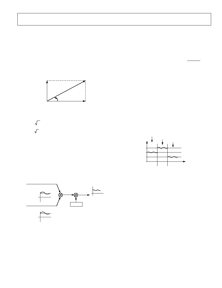
ADE7763
Rev. A | Page 31 of 56
APPARENT POWER CALCULATION
The apparent power is the maximum power that can be
delivered to a load. V
rms
and I
rms
are the effective voltage and
current delivered to the load; the apparent power (AP) is
defined as V
rms
× I
rms
. The angle between the active power and
the apparent power generally represents the phase shift due to
nonresistive loads. For single-phase applications, represents
the angle between the voltage and the current signals--see
Figure 63. Equation 24 gives an expression of the instantaneous
power signal in an ac system with a phase shift.
REACTIVE
POWER
APPARENT POWER
ACTIVE POWER
04481-A
-
064
Figure 63. Power Triangle
( )
2
sin( )
rms
v t
V
t
=
( )
2
sin(
)
rms
i t
I
t
=
+
(23)
)
(
)
(
)
(
t
i
t
v
t
p
×
=
)
2
cos(
)
cos(
)
(
+
-
=
t
I
V
I
V
t
p
rms
rms
rms
rms
(24)
The apparent power is defined as V
rms
× I
rms
. This expression is
independent from the phase angle between the current and
the voltage.
Figure 64 illustrates the signal processing in each phase for the
calculation of the apparent power in the ADE7763.
V
RMS
I
RMS
0xA D055
APPARENT POWER
SIGNAL (P)
CURRENT RMS SIGNAL i(t)
VOLTAGE RMS SIGNAL v(t)
MULTIPLIER
04481-A
-
065
0x00
0x1C 82B3
0x00
0x17 D338
VAGAIN
Figure 64. Apparent Power Signal Processing
The gain of the apparent energy can be adjusted by using the
multiplier and VAGAIN register (VAGAIN[11:0]). The gain is
adjusted by writing a twos complement, 12-bit word to the
VAGAIN register. Equation 25 shows how the gain adjustment
is related to the contents of the VAGAIN register.
+
×
=
12
2
1
VAGAIN
Power
Apparent
IN
OutputVAGA
(25)
For example, when 0x7FF is written to the VAGAIN register, the
power output is scaled up by 50%. 0x7FF = 2047d, 2047/2
12
= 0.5.
Similarly, 0x800 = 2047d (signed, twos complement) and power
output is scaled by 50%. Each LSB represents 0.0244% of the
power output. The apparent power is calculated with the current
and voltage rms values obtained in the rms blocks of the
ADE7763. Figure 65 shows the maximum code (hexadecimal)
output range of the apparent power signal. Note that the output
range changes depending on the contents of the apparent power
gain registers. The minimum output range is given when the
apparent power gain register content is equal to 0x800; the
maximum range is given by writing 0x7FF to the apparent
power gain register. This can be used to calibrate the apparent
power (or energy) calculation in the ADE7763.
0x10 3880
0xA D055
0x5 682B
0x0 0000
0x000
0x7FF
0x800
{VAGAIN[11:0]}
APPARENT POWER 100% FS
APPARENT POWER 150% FS
APPARENT POWER 50% FS
APPARENT POWER
CALIBRATION RANGE,
VOLTAGE AND CURRENT
CHANNEL INPUTS: 0.5V/GAIN
04481-A
-
066
Figure 65. Apparent Power Calculation Output Range
Apparent Power Offset Calibration
Each rms measurement includes an offset compensation
register to calibrate and eliminate the dc component in the rms
value--see the Channel 1 RMS Calculation and Channel 2 RMS
Calculation sections. The Channel 1 and Channel 2 rms values
are then multiplied together in the apparent power signal
processing. Because no additional offsets are created in the
multiplication of the rms values, there is no specific offset
compensation in the apparent power signal processing. The
offset compensation of the apparent power measurement is
done by calibrating each individual rms measurement.
ADE7763
Rev. A | Page 32 of 56
APPARENT ENERGY CALCULATION
The apparent energy is given as the integral of the
apparent power.
=
dt
t
Power
Apparent
Energy
Apparent
)
(
(26)
The ADE7763 achieves the integration of the apparent power
signal by continuously accumulating the apparent power signal
in an internal 49-bit register. The apparent energy register
(VAENERGY[23:0]) represents the upper 24 bits of this internal
register. This discrete time accumulation or summation is
equivalent to integration in continuous time. Equation 29
expresses this relationship.
×
=
=
0
0
)
(
n
T
T
nT
Power
Apparent
Lim
Energy
Apparent
(27)
where:
n
is the discrete number of time samples.
T
is the time sample period.
The discrete time sample period (T) for the accumulation
register is 1.1 µs (4/CLKIN).
Figure 66 shows this discrete time integration or accumulation.
The apparent power signal is continuously added to the internal
register. This addition is a signed addition, even if the apparent
energy always remains positive in theory.
The 49 bits of the internal register are divided by VADIV. If the
value in the VADIV register is 0, then the internal active energy
register is divided by 1. VADIV is an 8-bit, unsigned register.
The upper 24 bits are then written in the 24-bit apparent energy
register (VAENERGY[23:0]). RVAENERGY register (24 bits
long) is provided to read the apparent energy. This register is
reset to 0 after a read operation.
Figure 67 shows this apparent energy accumulation for full-
scale signals (sinusoidal) on the analog inputs. The three curves
illustrate the minimum time for the energy register to roll over
when the VAGAIN registers content is equal to 0x7FF, 0x000,
and 0x800. The VAGAIN register is used to carry out an
apparent power calibration. As shown in the figure, the fastest
integration time occurs when the VAGAIN register is set to
maximum full scale, i.e., 0x7FF.
VADIV
APPARENT
POWER
+
+
VAENERGY[23:0]
APPARENT POWER IS
ACCUMULATED (INTEGRATED) IN
THE APPARENT ENERGY REGISTER
23
0
48
0
48
0
04481-A
-
067
%
TIME (nT)
T
ACTIVE POWER
SIGNAL = P
Figure 66. Apparent Energy Calculation
0xFF FFFF
0x80 0000
0x40 0000
0x20 0000
0x00 0000
VAENERGY[23:0]
6.26
12.52
18.78
25.04
TIME
(minutes)
VAGAIN = 0x7FF
VAGAIN = 0x000
VAGAIN = 0x800
04481-A
-
068
Figure 67. Energy Register Rollover Time for Full-Scale Power
(Maximum and Minimum Power Gain)
Note that the apparent energy register is unsigned--see Figure
67. By using the interrupt enable register, the ADE7763 can be
configured to issue an interrupt (IRQ) when the apparent energy
register is more than half full or when an overflow occurs. The
half full interrupt for the unsigned apparent energy register is
based on 24 bits, as opposed to 23 bits for the signed active
energy register.
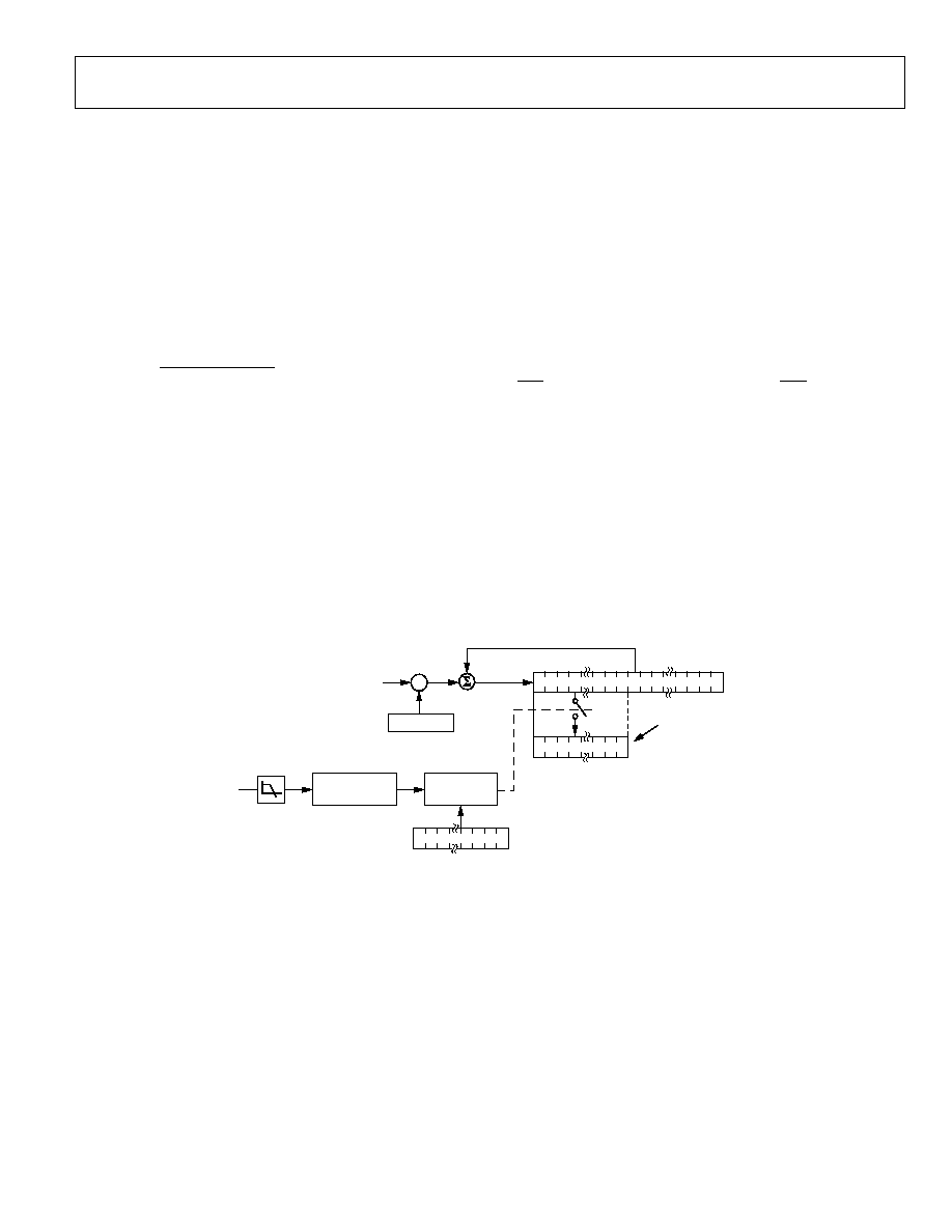
ADE7763
Rev. A | Page 33 of 56
Integration Times under Steady Load
As mentioned in the last section, the discrete time sample
period (T) for the accumulation register is 1.1 µs (4/CLKIN).
With full-scale sinusoidal signals on the analog inputs and the
VAGAIN register set to 0x000, the average word value from the
apparent power stage is 0xA D055. The maximum value that
can be stored in the apparent energy register before it overflows
is 2
24
or 0xFF FFFF. The average word value is added to the
internal register, which can store 2
48
or 0xFFFF FFFF FFFF
before it overflows. Therefore, the integration time under these
conditions with VADIV = 0 is calculated as follows:
min
52
.
12
888
2
.
1
0xAD055
FFFF
FFFF
0xFFFF
=
=
µ
×
=
s
s
Time
(28)
When VADIV is set to a value other than 0, the integration time
varies, as shown in Equation 29.
Time = Time
WDIV = 0
× VADIV (29)
LINE APPARENT ENERGY ACCUMULATION
The ADE7763 is designed with a special apparent energy
accumulation mode, which simplifies the calibration process.
By using the on-chip zero-crossing detection, the ADE7763
accumulates the apparent power signal in the LVAENERGY
register for an integral number of half cycles, as shown in
Figure 68. The line apparent energy accumulation mode is
always active.
The number of half line cycles is specified in the LINECYC
register, which is an unsigned, 16-bit register. The ADE7763 can
accumulate apparent power for up to 65,535 combined half
cycles. Because the apparent power is integrated on the same
integral number of line cycles as the line active energy register,
these two values can be easily compared. The active and apparent
energies are calculated more accurately because of this precise
timing control. At the end of an energy calibration cycle, the
CYCEND flag in the interrupt status register is set. If the
CYCEND mask bit in the interrupt mask register is enabled, the
IRQ output also will go active low. Thus, the IRQ line can also
be used to signal the end of a calibration.
The line apparent energy accumulation uses the same signal path
as the apparent energy accumulation. The LSB size of these two
registers is equivalent.
VADIV[7:0]
LPF1
+
+
LVAENERGY[23:0]
LVAENERGY REGISTER IS
UPDATED EVERY LINECYC
ZERO CROSSINGS WITH THE
TOTAL APPARENT ENERGY
DURING THAT DURATION
APPARENT
POWER
FROM
CHANNEL 2
ADC
23
0
LINECYC[15:0]
48
0
04481-A
-
069
%
ZERO-CROSSING
DETECTION
CALIBRATION
CONTROL
Figure 68. Apparent Energy Calibration
ADE7763
Rev. A | Page 34 of 56
ENERGIES SCALING
The ADE7763 provides measurements of active and apparent
energies. These measurements do not have the same scaling and
therefore cannot be compared directly to each other.
Table 7. Energies Scaling
PF = 1
PF = 0.707
PF = 0
Integrator on at 50 Hz
Active
Wh
Wh × 0.707
0
Apparent
Wh × 0.848
Wh × 0.848
Wh × 0.848
Integrator off at 50 Hz
Active
Wh
Wh × 0.707
0
Apparent
Wh × 0.848
Wh × 0.848
Wh × 0.848
Integrator on at 60 Hz
Active
Wh
Wh × 0.707
0
Apparent
Wh × 0.827
Wh × 0.827
Wh × 0.827
Integrator off at 60 Hz
Active
Wh
Wh × 0.707
0
Apparent
Wh × 0.827
Wh × 0.827
Wh × 0.827
CALIBRATING AN ENERGY METER
The ADE7763 provides gain and offset compensation for active
and apparent energy calibration. Its phase compensation corrects
phase error in active and apparent energy. If a shunt is used,
offset and phase calibration may not be required. A reference
meter or an accurate source can be used to calibrate
the ADE7763.
When using a reference meter, the ADE7763 calibration output
frequency, CF, is adjusted to match the frequency output of the
reference meter. A pulse output is only provided for the active
energy measurement in the ADE7763. If a reference meter is
used to calibrate the VA, then additional code must be written
in a microprocessor to produce a pulsed output for this
quantity. Otherwise, VA calibration requires an accurate source.
The ADE7763 provides a line cycle accumulation mode for
calibration using an accurate source. In this method, the active
energy accumulation rate is adjusted to produce a desired CF
frequency. The benefit of using this mode is that the effect of the
ripple noise on the active energy is eliminated. Up to 65,535 half
line cycles can be accumulated, therefore providing a stable
energy value to average. The accumulation time is calculated
from the line cycle period, measured by the period register, and
the number of half line cycles in the accumulation, fixed by the
LINECYC register.
Current and voltage rms offset calibration removes apparent
energy offset. A gain calibration is also provided for apparent
energy. Figure 70 shows an optimized calibration flow for active
energy, rms, and apparent energy.
Active and apparent energy gain calibrations can take place
concurrently, with a read of the accumulated apparent energy
register following that of the accumulated active energy register.
Figure 69 shows the calibration flow for the active energy
portion of the ADE7763.
WATT GAIN CALIBRATION
WATT OFFSET CALIBRATION
PHASE CALIBRATION
04481-
A
-
083
Figure 69. Active Energy Calibration
WATT/VA GAIN CALIBRATION
WATT OFFSET CALIBRATION
RMS CALIBRATION
PHASE CALIBRATION
04481-A-084
Figure 70. Apparent and Active Energy Calibration

ADE7763
Rev. A | Page 35 of 56
Watt Gain
The first step of calibrating the gain is to define the line voltage,
the base current, and the maximum current for the meter. A
meter constant, such as 3200 imp/kWh or 3.2 imp/Wh, needs to
be determined for CF. Note that the line voltage and the
maximum current scale to half of their respective analog input
ranges in this example.
The expected CF in Hz is
CF
expected
(Hz) =
)
cos(
s/h
3600
)
W
(
)
imp/Wh
(
×
× Load
ant
MeterConst
(30)
where:
is the angle between I and V.
cos
is the power factor.
)
(
The ratio of active energy LSBs per CF pulse is adjusted using
the CFNUM, CFDEN, and WDIV registers.
CF
expected
=
)
1
(
)
1
(
(s)
+
+
×
×
CFDEN
CFNUM
WDIV
onTime
Accumulati
LAENERGY
(31)
The relationship between watt-hours accumulated and the
quantity read from AENERGY can be determined from the
amount of active energy accumulated over time with a
given load:
s/h
3600
)
(
(W)
LSB
Wh
×
×
=
LAENERGY
s
Time
on
Accumulati
Load
(32)
where Accumulation Time can be determined from the value in
the line period and the number of half line cycles fixed in the
LINECYC register.
Accumulation time(s) =
2
)
(s
Period
Line
LINECYC
IB
×
(33)
The line period can be determined from the period register:
Line Period(s) = PERIOD ×
CLKIN
8
(34)
The AENERGY Wh/LSB ratio can also be expressed in terms of
the meter constant:
(imp/Wh)
)
1
(
)
1
(
LSB
Wh
ant
MeterConst
WDIV
CFDEN
CFNUM
×
+
+
=
(35)
In a meter design, WDIV, CFNUM, and CFDEN should be kept
constant across all meters to ensure that the Wh/LSB constant is
maintained. Leaving WDIV at its default value of 0 ensures
maximum resolution. The WDIV register is not included in the
CF signal chain, so it does not affect the frequency pulse output.
The WGAIN register is used to finely calibrate each meter. Cali-
brating the WGAIN register changes both CF and AENERGY for
a given load condition.
AENERGY
expected
= AENERGY
nominal
×
+
12
2
1
WGAIN
(36)
CF
expected
(Hz) = CF
nominal
×
+
×
+
+
12
2
1
)
1
(
)
1
(
WGAIN
CFDEN
CFNUM
(37)
When calibrating with a reference meter, WGAIN is adjusted
until CF matches the reference meter pulse output. If an
accurate source is used to calibrate, WGAIN will be modified
until the active energy accumulation rate yields the expected CF
pulse rate.
The steps of designing and calibrating the active energy portion
of a meter with either a reference meter or an accurate source
are outlined in the following examples. The specifications for
this example are
Meter Constant:
MeterConstant(imp/Wh) = 3.2
Base
Current:
I
b
= 10 A
Maximum Current:
I
MAX
= 60 A
Line
Voltage:
V
nominal
= 220 V
Line Frequency:
f
l
= 50 Hz
The first step in calibration with either a reference meter or an
accurate source is to calculate the CF denominator, CFDEN.
This is done by comparing the expected CF pulse output to the
nominal CF output with the default CFDEN = 0x3F and
CFNUM = 0x3F when the base current is applied.
The expected CF output for this meter with the base current
applied is 1.9556 Hz using Equation 30.
CF
IB(expected)
(Hz) =
Hz
9556
.
1
)
cos(
s/h
3600
V
220
A
10
imp/Wh
200
.
3
=
×
×
×
Alternatively, CF
expected
can be measured from a reference meter
pulse output.
CF
expected
(Hz) = CF
ref
(38)
The maximum CF frequency measured without any frequency
division and with ac inputs at full scale is 23 kHz. For this
example, the nominal CF with the test current, I
b
, applied is
958 Hz. In this example the line voltage and maximum current
scale half of their respective analog input ranges. The line
voltage and maximum current should not be fixed at the
maximum analog inputs to account for occurrences such as
spikes on the line.

ADE7763
Rev. A | Page 36 of 56
CF
nominal
(Hz) =
MAX
I
I
×
×
×
2
1
2
1
kHz
23
(39)
CF
IB(nominal)
(Hz) =
Hz
958
60
10
2
1
2
1
kHz
23
=
×
×
×
The nominal CF on a sample set of meters should be measured
using the default CFDEN, CFNUM, and WDIV to ensure that
the best CFDEN is chosen for the design.
With the CFNUM register set to 0, CFDEN is calculated to be
489 for the example meter:
CFDEN =
1
)
(
)
(
-
expected
IB
nominal
IB
CF
CF
INT
(40)
CFDEN =
489
)
1
490
(
1
9556
.
1
958
=
-
=
-
INT
This value for CFDEN should be loaded into each meter before
calibration. The WGAIN register can then be used to finely
calibrate the CF output. The following sections explain how to
calibrate a meter based on ADE7763 when using a reference
meter or an accurate source.
Calibrating Watt Gain Using a Reference Meter Example
The CFDEN and CFNUM values for the design should be
written to their respective registers before beginning the
calibration steps shown in Figure 71. When using a reference
meter, the percent error in CF is measured by comparing the CF
output of the ADE7763 meter with the pulse output of the
reference meter, using the same test conditions for both meters.
Equation 41 defines the percent error with respect to the pulse
outputs of both meters (using the base current, I
b
):
%ERROR
CF(IB)
=
100
)
(
)
(
×
-
IB
ref
IB
ref
IB
CF
CF
CF
(41)
CALCULATE CFDEN VALUE FOR DESIGN
WRITE CFDEN VALUE TO CFDEN REGISTER
ADDR. 0x15 = CFDEN
WRITE WGAIN VALUE TO THE WGAIN
REGISTER: ADDR. 0x12
MEASURE THE % ERROR BETWEEN
THE CF OUTPUT AND THE
REFERENCE METER OUTPUT
SET I
TEST
= I
b
, V
TEST
= V
NOM
, PF = 1
04481-A
-
085
CALCULATE WGAIN. SEE EQUATION 42.
Figure 71. Calibrating Watt Gain Using a Reference Meter
For this example:
Meter Constant:
MeterConstant(imp/Wh) = 3.2
CF Numerator:
CFNUM = 0
CF Denominator:
CFDEN = 489
%ERROR Measured at Base Current:
%ERROR
CF(IB)
= -3.07%
One LSB change in WGAIN changes the active energy registers
and CF by 0.0244%. WGAIN is a signed, twos complement
register and can correct up to a 50% error. Assuming a -3.07%
error, WGAIN is 126:
WGAIN = INT
-
%
0244
.
0
%
)
(IB
CF
ERROR
(42)
WGAIN = INT
126
%
0244
.
0
%
07
.
3
=
-
-
When CF is calibrated, the AENERGY register has the same
Wh/LSB constant from meter to meter if the meter constant,
WDIV, and the CFNUM/CFDEN ratio remain the same. The
Wh/LSB ratio for this meter is 6.378 × 10
-4
using Equation 35
with WDIV at the default value.
(imp/Wh)
)
1
(
)
1
(
LSB
Wh
ant
MeterConst
WDIV
CFDEN
CFNUM
×
+
+
=
4
10
378
.
6
2
.
3
490
1
imp/Wh
200
.
3
)
1
490
(
1
LSB
Wh
-
×
=
×
=
+
=
Calibrating Watt Gain Using an Accurate Source Example
The CFDEN value calculated using Equation 40 should be
written to the CFDEN register before beginning calibration and
zero should be written to the CFNUM register. Enable the line
accumulation mode and the line accumulation interrupt. Then,
write the number of half line cycles for the energy accumulation
to the LINECYC register to set the accumulation time. Reset the
interrupt status register and wait for the line cycle accumulation
interrupt. The first line cycle accumulation results might not
use the accumulation time set by the LINECYC register and,
therefore, should be discarded. After resetting the interrupt
status register, the following line cycle readings will be valid.
When LINECYC half line cycles have elapsed, the IRQ pin goes
active low and the nominal LAENERGY with the test current
applied can be read. This LAENERGY value is compared to the
expected LAENERGY value to determine the WGAIN value. If
apparent energy gain calibration is performed at the same time,
LVAENERGY can be read directly after LAENERGY. Both
registers should be read before the next interrupt is issued on
the IRQ pin. Figure 72 details steps to calibrate the watt gain
using an accurate source.
ADE7763
Rev. A | Page 37 of 56
WRITE WGAIN VALUE TO THE WGAIN
REGISTER: ADDR. 0x12
CALCULATE CFDEN VALUE FOR DESIGN
WRITE CFDEN VALUE TO CFDEN REGISTER
ADDR. 0x15 = CFDEN
SET HALF LINE CYCLES FOR ACCUMULATION
IN LINECYC REGISTER ADDR. 0x1C
SET I
TEST
= I
b
, V
TEST
= V
NOM
, PF = 1
CALCULATE WGAIN. SEE EQUATION 43.
SET MODE FOR LINE CYCLE
ACCUMULATION ADDR. 0x09 = 0x0080
ENABLE LINE CYCLE ACCUMULATION
INTERRUPT ADDR. 0x0A = 0x04
READ LINE ACCUMULATION ENERGY
ADDR. 0x04
RESET THE INTERRUPT STATUS
READ REGISTER ADDR. 0x0C
INTERRUPT?
NO
NO
YES
YES
04481-A
-
086
RESET THE INTERRUPT STATUS
READ REGISTER ADDR. 0x0C
INTERRUPT?
Figure 72. Calibrating Watt Gain Using an Accurate Source
Equation 43 describes the relationship between the expected
LAENERGY value and the LAENERGY measured in the test
condition:
WGAIN = INT
×
-
12
)
(
)
(
2
1
nominal
IB
expected
IB
LAENERGY
LAENERGY
(43)
The nominal LAENERGY reading, LAENERGY
IB(nominal)
, is the
LAENERGY reading with the test current applied. The expected
LAENERGY reading is calculated from the following equation:
LAENERGY
IB(expected)
=
INT
×
+
+
×
WDIV
CFDEN
CFNUM
Time
on
Accumulati
CF
expected
IB
1
1
(s)
)
(
(44)
where CF
IB(expected)
(Hz) is calculated from Equation 30,
accumulation time is calculated from Equation 33, and the line
period is determined from the period register according to
Equation 34.
For this example:
Meter Constant:
MeterConstant(imp/Wh) = 3.2
Test
Current:
I
b
= 10 A
Line
Voltage:
V
nominal
= 220 V
Line Frequency:
f
l
= 50 Hz
Half Line Cycles:
LINECYC
IB
= 2000
CF Numerator:
CFNUM = 0
CF Denominator:
CFDEN = 489
Energy Reading at Base Current:
LAENERGY
IB (nominal)
= 17174
Period Register Reading:
PERIOD = 8959
Clock Frequency:
CLKIN = 3.579545 MHz
CF
expected
is calculated to be 1.9556 Hz according to Equation 30.
LAENERGY
expected
is calculated to be 19186 using Equation 44.
CF
IB(expected)
(Hz) =
)
cos(
s/h
3600
A
10
V
220
imp/Wh
200
.
3
×
×
×
= 1.9556 Hz
LAENERGY
IB(expected)
=
INT
×
+
+
×
×
×
WDIV
CFDEN
CFNUM
CLKIN
PERIOD
LINECYC
CF
IB
expected
IB
1
1
/
8
2
/
)
(
LAENERGY
IB(expected)
=
INT
1
1
489
1
)
10
579545
.
3
/(
8
8959
2
/
2000
9556
.
1
6
+
×
×
×
×
=
19186
)
4
.
19186
(
=
INT

ADE7763
Rev. A | Page 38 of 56
WGAIN is calculated to be 480 using Equation 43.
WGAIN = INT
480
2
1
17174
19186
12
=
×
-
Note that WGAIN is a signed, twos complement register.
With
WDIV and CFNUM set to 0, LAENERGY can be
expressed as
LAENERGY
IB(expected)
=
))
1
(
/
8
2
/
(
)
(
+
×
×
×
×
CFDEN
CLKIN
PERIOD
LINECYC
CF
INT
IB
expected
IB
The calculated Wh/LSB ratio for the active energy register,
using Equation 35 is 6.378 × 10
-4
is
4
10
378
.
6
imp/Wh
200
.
3
)
1
489
(
1
LSB
Wh
-
×
=
+
=
Watt Offset
Offset calibration allows outstanding performance over a wide
dynamic range, for example, 1000:1. To do this calibration two
measurements are needed at unity power factor, one at I
b
and
the other at the lowest current to be corrected. Either calibra-
tion frequency or line cycle accumulation measurements can be
used to determine the energy offset. Gain calibration should be
performed prior to offset calibration.
Offset calibration is performed by determining the active energy
error rate. After determining the active energy error rate, calcu-
late the value to write to the APOS register to correct the offset.
APOS = -
CLKIN
Rate
Error
AENERGY
35
2
×
(45)
The AENERGY registers update at a rate of CLKIN/4. The twos
complement APOS register provides a fine adjustment to the
active power calculation. It represents a fixed amount of power
offset to be adjusted every CLKIN/4. The 8 LSBs of the APOS
register are fractional such that one LSB of APOS represents
1/256 of the least significant bit of the internal active energy
register. Therefore, one LSB of the APOS register represents 2
-33
of the AENERGY[23:0] active energy register.
See the following sections for steps to determine the active
energy error rate for both line accumulation and reference
meter calibration options.
Calibrating Watt Offset Using a Reference Meter Example
Figure 73 shows the steps involved in calibrating watt offset
with a reference meter.
WRITE APOS VALUE TO THE APOS
REGISTER: ADDR. 0x11
MEASURE THE % ERROR BETWEEN THE
CF OUTPUT AND THE REFERENCE METER
OUTPUT, AND THE LOAD IN WATTS
SET I
TEST
= I
MIN
, V
TEST
= V
NOM
, PF = 1
04481-A
-
087
CALCULATE APOS. SEE EQUATION 45.
Figure 73. Calibrating Watt Offset Using a Reference Meter
For this example:
Meter
Constant:
MeterConstant(imp/Wh) = 3.2
Minimum Current:
I
MIN
= 40 mA
Load at Minimum Current:
W
IMIN
= 9.6 W
CF Error at Minimum Current: %
ERROR
CF(IMIN)
= 1.3%
CF
Numerator:
CFNUM = 0
CF
Denominator:
C
DEN = 489
Clock Frequency:
C
KIN = 3.579545 MHz
Using Equation 45,
APOS is -522 for this example.
CF Absolute Error = CF
IMIN(nominal)
- CF
IMIN(expected)
(46)
CF Absolute Error =
(%
ERROR
CF(IMIN)
) ×
W
IMIN
×
3600
(imp/Wh)
ant
MeterConst
(47)
CF Absolute Error =
Hz
000110933
.
0
3600
200
.
3
6
.
9
100
%
3
.
1
=
×
×
Then,
AENERGY Error Rate (LSB/s) =
CF Absolute Error ×
1
1
+
+
CFNUM
CFDEN
(48)
AENERGY Error Rate (LSB/s) =
0.000110933 ×
05436
.
0
1
490 =
Using Equation 45, APOS is -522.
APOS = -
522
10
579545
.
3
2
05436
.
0
6
35
-
=
×
×
APOS can be represented as follows with CFNUM and WDIV
set at 0:
APOS =
-
CLKIN
CFDEN
ant
MeterConst
W
ERROR
IMIN
IMIN
CF
35
)
(
2
)
1
(
3600
(imp/Wh)
)
(%
×
+
×
×
×
ADE7763
Rev. A | Page 39 of 56
Calibrating Watt Offset with an Accurate Source Example
Figure 74 is the flowchart for watt offset calibration with an
accurate source.
SET HALF LINE CYCLES FOR ACCUMULATION
IN LINECYC REGISTER ADDR. 0x1C
SET I
TEST
= I
MIN
, V
TEST
= V
NOM
, PF = 1
CALCULATE APOS. SEE EQUATION 45.
SET MODE FOR LINE CYCLE
ACCUMULATION ADDR. 0x09 = 0x0080
ENABLE LINE CYCLE ACCUMULATION
INTERRUPT ADDR. 0x0A = 0x04
READ LINE ACCUMULATION ENERGY
ADDR. 0x04
RESET THE INTERRUPT STATUS
READ REGISTER ADDR. 0x0C
INTERRUPT?
NO
NO
YES
YES
RESET THE INTERRUPT STATUS
READ REGISTER ADDR. 0x0C
INTERRUPT?
WRITE APOS VALUE TO THE APOS
REGISTER: ADDR. 0x11
04481-A
-
088
Figure 74. Calibrating Watt Offset with an Accurate Source
For this example:
Meter Constant:
MeterConstant(imp/Wh) = 3.2
Line
Voltage:
V
nominal
= 220 V
Line Frequency:
f
l
= 50 Hz
CF Numerator:
CFNUM = 0
CF Denominator:
CFDEN = 489
Base
Current:
I
b
= 10 A
Half Line Cycles Used at Base Current:
LINECYC
(IB)
= 2000
Period Register Reading:
PERIOD = 8959
Clock Frequency:
CLKIN = 3.579545 MHz
Expected LAENERGY Register Value at Base Current
(from the Watt Gain section):
LAENERGY
IB(expected)
= 19186
Minimum Current:
I
MIN
= 40 mA
Number of Half Line Cycles used at Minimum Current:
LINECYC
(IMIN)
= 35700
Active Energy Reading at Minimum Current:
LAENERGY
IMIN(nominal)
= 1395
The LAENERGY
expected
at I
MIN
is 1255 using Equation 49.
LAENERGY
IMIN(expected)
=
INT
×
×
IB
MIN
expected
IB
B
MIN
LINECYC
LINECYCI
LAENERGY
I
I
)
(
(49)
LAENERGY
IMIN(expected)
=
INT
1370
)
80
.
1369
(
2000
35700
19186
10
04
.
0
=
=
×
×
INT
where:
LAENERGY
IB(expected)
is the expected LAENERGY reading at I
b
from the watt gain calibration.
LINECYC
IMIN
is the number of half line cycles that energy is
accumulated over when measuring at I
MIN
.
More line cycles could be required at the minimum current to
minimize the effect of quantization error on the offset calibration.
For example, if a test current of 40 mA results in an active energy
accumulation of 113 after 2000 half line cycles, one LSB variation
in this reading represents a 0.8% error. This measurement does
not provide enough resolution to calibrate a <1% offset error.
However, if the active energy is accumulated over 37,500 half
line cycles, one LSB variation results in 0.05% error, reducing the
quantization error.
APOS is -672 using Equations 55 and 49.
LAENERGY Absolute Error =
LAENERGY
IMIN(nominal)
- LAENERGY
IMIN(expected)
LAENERGY Absolute Error = 1395 - 1370 = 25
(50)
AENERGY Error Rate (LSB/s) =
PERIOD
CLKIN
LINECYC
Error
Absolute
LAENERGY
×
×
8
2
/
(51)
AENERGY Error Rate (LSB/s) =
069948771
.
0
8959
8
10
579545
.
3
2
/
35700
25
6
=
×
×
×
CLKIN
Rate
Error
AENERGY
35
2
×
APOS = -
672
10
579545
.
3
2
069948771
.
0
6
35
-
=
×
×
APOS = -
ADE7763
Rev. A | Page 40 of 56
mpensates for phase error by inserting a small
time delay or advance on the voltage channel input. Phase leads
up to 1.84° and phase lags up to 0.72° at 50 Hz can be corrected.
The error is determined by measuring the active energy at I
B
and
two power factors, PF = 1 and PF = 0.5 inductive.
Some CTs may introduce large phase errors that are beyond the
range of the phase calibration register. In this case, coarse phase
compensation has to be done externally with an analog filter.
The phase error can be obtained from either CF or LAENERGY
measurements:
Error =
Phase Calibration
The PHCAL register is provided to remove small phase errors.
The ADE7763 co
2
2
)
(
)
(
5
.
0
,
expected
IB
expected
IB
PF
IB
LAENERGY
LAENERGY
LAENERGY
-
=
(52)
If watt gain and offset calibration have been performed, there
should be 0% error in CF at unity power factor, and then
Error = %ERROR
CF(IB,PF = 0.5)
/100 (53)
The phase error is
Phase Error (°) = -Arcsin
3
Error
(54)
The relationship between phase error and the PHCAL phase
correction register is
PHCAL = INT
( )
+
°
×
°
360
PERIOD
Error
Phase
0x0D
(55)
The expression for PHCAL can be simplified using the
assumption that at small x
Arcsin(x) x
d in the voltage channel by PHCAL is
AL - 0x0D) × 8/
s a time delay if
sit e, b
ts a time advance if this
ve
he is
f PHCAL = 0x0D.
ction of the
)
The delay introduce
Delay = (PHC
CLKIN (56)
The delay associated with the PHCAL register i
PHCAL - 0x0D is po iv
ut represen
quantity is negati . T re no time delay i
The phase correction is in the opposite dire
phase error.
Phase Correction (°) = - (PHCAL - 0x0D
PER
Calibrating Phase Using a Reference Meter Example
A power factor of 0.5 inductive can be assumed if the
output rate of the reference meter is half of its PF
r
Then, the percent error between CF and the pulse output o
IOD
°
× 360
(57)
pulse
= 1 ate.
f
r ca
the reference mete
n be used to perform the preceding
calculations.
WRITE PHCAL VALUE TO THE PHCAL
REGISTER: ADDR. 0x10
MEASURE THE % ERROR BETWEEN
THE CF OUTPUT AND THE
REFERENCE METER OUTPUT
SET I
TEST
= I
b
, V
TEST
= V
NOM
, PF = 0.5
04481-A
-089
CALCULATE PHCAL. SEE EQUATION 55.
Figure 75. Calibrating Phase Using a Reference Meter
For this example:
CF %ERROR at PF = 0.5 Inductive: %ERROR
CF(IB,PF = 0.5)
= 0.215%
PERIOD Register Reading:
PERIOD = 8959
Then PHCAL is 11 using Equations 57 through 59:
Error = 0.215%/100 = 0.00215
Phase Error (°) = -Arcsin
°
-
=
07
.
0
3
00215
.
0
PHCAL = INT
°
×
°
-
360
8959
07
.
0
+0x0D = -2 + 13 = 11
PHCAL can be expressed as follows:
PHCAL =
INT
×
×
-
2
3
100
%
Arcsin
PERIOD
ERROR
+
(58)
0x0D
Note that PHCAL is a signed, twos complement register.
Setting the PHCAL register to 11 provides a phase correction
of 0.08° t
Phase Correction (°) = -
o correct the phase lead:
PERIOD
PHCAL
°
×
-
360
)
0x0D
(
Phase Corr
°
=
°
×
-
08
.
0
8960
360
)
0x0D
11
(
ection (°) = -
ADE7763
Rev. A | Page 41 of 56
ith an Accurate Source Example
Calibrating Phase w
With an accurate source, line cycle accumulation is a good
method of calibrating phase error. The value of LAENERGY
must be obtained at two power factors, PF = 1 and PF = 0.5
inductive.
SET HALF LINE CYCLES FOR ACCUMULATION
IN LINECYC REGISTER ADDR. 0x1C
SET I
TEST
= I
b
, V
TEST
= V
NOM
, PF = 0.5
CALCULATE PHCAL. SEE EQUATION 55.
SET MODE FOR LINE CYCLE
ACCUMULATION ADDR. 0x09 = 0x0080
ENABLE LINE CYCLE ACCUMULATION
INTERRUPT ADDR. 0x0A = 0x04
READ LINE ACCUMULATION ENERGY
ADDR. 0x04
RESET THE INTERRUPT STATUS
READ REGISTER ADDR. 0x0C
INTERRUPT?
NO
NO
YES
YES
RESET THE INTERRUPT STATUS
READ REGISTER ADDR. 0x0C
INTERRUPT?
WRITE PHCAL VALUE TO THE PHCAL
-
090
For this example:
Line Frequency:
f = 50 Hz
tor:
CFDEN = 489
Base
Current:
I
b
= 10 A
Half
LINECYC
IB
= 2000
PERI D Register:
PERIOD = 8959
Expected Line Accumulation at Unity Power Factor (from Watt
Gain ection):
LAENERGY
IB(expected)
= 19186
Acti Energy Reading at PF = 0.5 inductive:
LAENERGY
IB, PF = 0.5
= 9613
REGISTER: ADDR. 0x10
04481-A
Figure 76. Calibrating Phase with an Accurate Source
Meter Constant:
MeterConstant(imp/Wh) = 3.2
Line
Voltage:
V
nominal
= 220 V
L
CF Numerator:
CFNUM = 0
CF Denomina
Line Cycles Used at Base Current:
O
s
ve
The error using Equation 52 is
Error =
0021
.
0
2
19186
2
19186
9613
=
-
Phase Er
°
-
=
07
.
0
3
0021
.
0
ror (°) = -Arcsin
Using Equation 55, PHCAL is 11.
PHCAL = INT
11
13
2
0x0D
360
8959
07
.
0
=
+
-
=
+
°
×
°
-
Note that PHCAL is a signed, twos complement register.
The phase lead is corrected by 0.08 degrees when the PHCAL
register is set to 11:
n (°) = -
Phase Correctio
PERIOD
PHCAL
°
×
-
360
)
0x0D
(
Phase Correction (°) = -
°
=
°
×
-
08
.
0
8960
360
)
0x0D
11
(
VRMS and IRMS Calibration
VRMS and IRMS are calculated by squaring the input in a
digital multiplier.
)
2
cos(
)
sin(
V
2
)
sin(
V
2
)
(
t
t
v
2
×
×
=
t
V
V
t
2
2
-
=
(59)
The s
s value is extract
2
ass
filter
t of the output o
s
the rms value. An offset correction is provided to cancel noise
t.
Ther
oise from the 2 term because the low-pass
filter does not completely attenuate the signal. This noise can be
min
by synchronizing the rms register readi
zero crossing of the voltage signal. The IRQ
quare of the rm
ed from v (t) by a low-p
. The square roo
f this low-pass filter give
and offset contributions from the inpu
e is ripple n
imized
ngs with the
output can be
al.
ngs of the voltage input.
configured to indicate the zero crossing of the voltage sign
This flowchart demonstrates how VRMS and IRMS readings
are synchronized to the zero crossi
ADE7763
Rev. A | Page 42 of 56
2
1
2
2
2
1
2
2
2
2
2
1
IRMS
I
×
×
1
SET INTERRUPT ENABLE FOR ZERO
IRMSOS =
I
I
IRMS
I
-
×
-
32768
(63)
whe
and IRMS
2
are rms regis r values without offset
correction for input I
1
and I
2
, respectively.
App
Apparent energy gain calibration is provided for both meter-to-
g the VAh/LSB constant.
VAENERGY =
CROSSING ADDR. 0x0A = 0x0010
RESET THE INTERRUPT STATUS
READ REGISTER ADDR. 0x0C
re IRMS
1
te
INTERRUPT?
NO
YES
04481-
A-
091
READ VRMS OR IRMS
ADDR. 0x17; 0x16
RESET THE INTERRUPT STATUS
READ REGISTER ADDR. 0x0C
Figure 77. Synchronizing VRMS and IRMS Readings with Zero Crossings
Voltage rms compensation is done after the square root.
VRMS = VRMS0 + VRMSOS
(60)
where:
VRMS0 is the rms measurement without offset correction.
VRMS is linear from full-scale to full-scale/20.
To calibrate the offset, two VRMS measurements are required,
for example, at V
nominal
and V
nominal
/10. V
nominal
is set at half of the
full-scale analog input range so that the smallest linear VRMS
reading is at V
nominal
/10.
VRMSOS =
arent Energy
meter gain adjustment and for settin
+
×
×
12
2
1
1
VAGAIN
VADIV
VAENERGY
initial
(64)
tion. It
used to calibrate individual meters.
App
ion should be performed bef
rms
the most efficient use of the c rent
test points. Apparent energy gain and watt gain compensation
requ
s and watt offset correction equire
a lower test current. Apparent energy gain calibration can be
tt-hour gain calibration
line cycle accumulation apparent energy
registers, are both read following the line cycle accumulation
interrupt. Figure 78 shows a flowchart for calibrating active and
appa
VADIV is similar to the CFDEN for the watt-hour calibra
should be the same across all meters and determines the VAh/LSB
constant. VAGAIN is
arent energy gain calibrat
ore
offset correction to make
ur
ire testing at I
b
, while rm
r
done simultaneously with the wa
using line cycle accumulation. In this case, LAENERGY and
LVAENERGY, the
rent energy simultaneously.
1
2
2
2
1
V
V
VRMS
V
VRMS
V
-
×
-
×
1
(61)
where VRMS
1
and VRMS
2
are rms register values without offset
correction for input V
1
and V
2
, respectively.
If the range of the 12-bit, twos complement VRMSOS register is
not enough, use the voltage channel offset register, CH2OS, to
correct the VRMS offset.
Current rms compensation is performed before the square root:
IRMS
2
= IRMS0
2
+ 32768 × IRMSOS
(62)
ut offset correction.
a ula
n
m full scale to full
ts are required,
at alf of the full-scale
S reading is at
VAGAIN = INT
×
-
12
)
(
)
(
2
1
nominal
IB
expected
IB
LVAENERGY
LVAENERGY
(65
LVAENERGY
)
IB(expected)
=
INT
×
×
×
)
(
s/h
3600
s
time
on
Accumulati
constant
LSB
VAh
I
V
B
nominal
(6
6)
according to Equation 34. The VAh represented by the
VAENERGY register is
VAh = VAENERGY × VAh/LSB constant
(67)
The VAh/LSB constant can be verified using this equation:
The accumulation time is determined from Equation 33, and
the line period can be determined from the period register
where IRMS0 is the rms measurement witho
The current rms c lc
tio is linear fro
scale/100.
To calibrate this offset, two IRMS measuremen
for example, at I
b
and I
MAX
/50. I
MAX
is set h
analog input range so that the smallest linear IRM
I
MAX
/50.
LVAENERGY
s
time
on
Accumulati
VA
constant
LSB
VAh
3600
)
(
×
=
(68)
ADE7763
Rev. A | Page 43 of 56
CALCULATE CFDEN VALUE FOR DESIGN
WRITE CFDEN VALUE TO CFDEN REGISTER
ADDR. 0x15 = CFDEN
SET HALF LINE CYCLES FOR ACCUMULATION
IN LINECYC REGISTER ADDR. 0x1C
SET I
TEST
= I
b
, V
TEST
= V
NOM
, PF = 1
CALCULATE WGAIN. SEE EQUATION 43.
SET MODE FOR LINE CYCLE
ACCUMULATION ADDR. 0x09 = 0x0080
ENABLE LINE CYCLE ACCUMULATION
INTERRUPT ADDR. 0x0A = 0x04
READ LINE A
ACTIVE ENERGY: ADDR. 0x04
APPARENT ENERGY: ADDR. 0x07
CCUMULATION ENERGY
RESET THE INTERRUPT STATUS
READ REGISTER ADDR. = 0x0C
INTERRUPT?
NO
YES
RESET THE INTERRUPT STA
READ REGIS
TUS
TER ADDR. = 0x0C
NO
INTERRUPT?
YES
WRITE WGAIN VALUE TO ADDR. 0x12
04481-A
-
092
CALCULATE VAGAIN. SEE EQUATION 65.
WRITE VGAIN VALUE TO ADDR. 0x1A
Figure 78. Active/Apparent
In th
ADE7763 are sh
cy is
5 MHz, various timing and filter characteristics will
equency according to the following equation:
Gain Calibration
CLKIN FREQUENCY
is data sheet, the characteristics of the
own
when CLKIN frequency equals 3.579545 MHz. However, the
ADE7763 is designed to have the same accuracy at any CLKIN
frequency within the specified range. If the CLKIN frequen
not 3.57954
need to be redefined with the new CLKIN frequency. For
example, the cutoff frequencies of all digital filters, such as
LPF1, LPF2, or HPF1, shift in proportion to the change in
CLKIN fr
MHz
Frequency
New
579545
.
3
Frequency
CLKIN
Frequency
Original
×
=
(69)
The change in CLKIN frequency does not affect the timing
characteristics of the serial interface because the data transfer is
ever, it is
e read/write timing of the serial data
tran
le 2. Table 8 li
y.
Table 8. Frequency Dependencies of the ADE7763 Parameters
Parameter CLKIN
Dependency
synchronized with the serial clock signal (SCLK). How
important to observe th
sfer--see the timing characteristics in Tab
sts
various timing changes that are affected by CLKIN frequenc
Nyquist Frequency for CH 1, CH 2 ADCs
CLKIN/8
PHCAL Resolution (seconds per LSB)
4/CLKIN
Active Energy Register Update Rate (Hz)
CLKIN/4
Waveform Sampling Rate (per second)
WAVSEL 1,0 = 0 0
CLKIN/128
0
1
CLKIN/256
1
0
CLKIN/512
1
1
CLKIN/1024
Maximum ZXTOUT Period
524,288/CLKIN
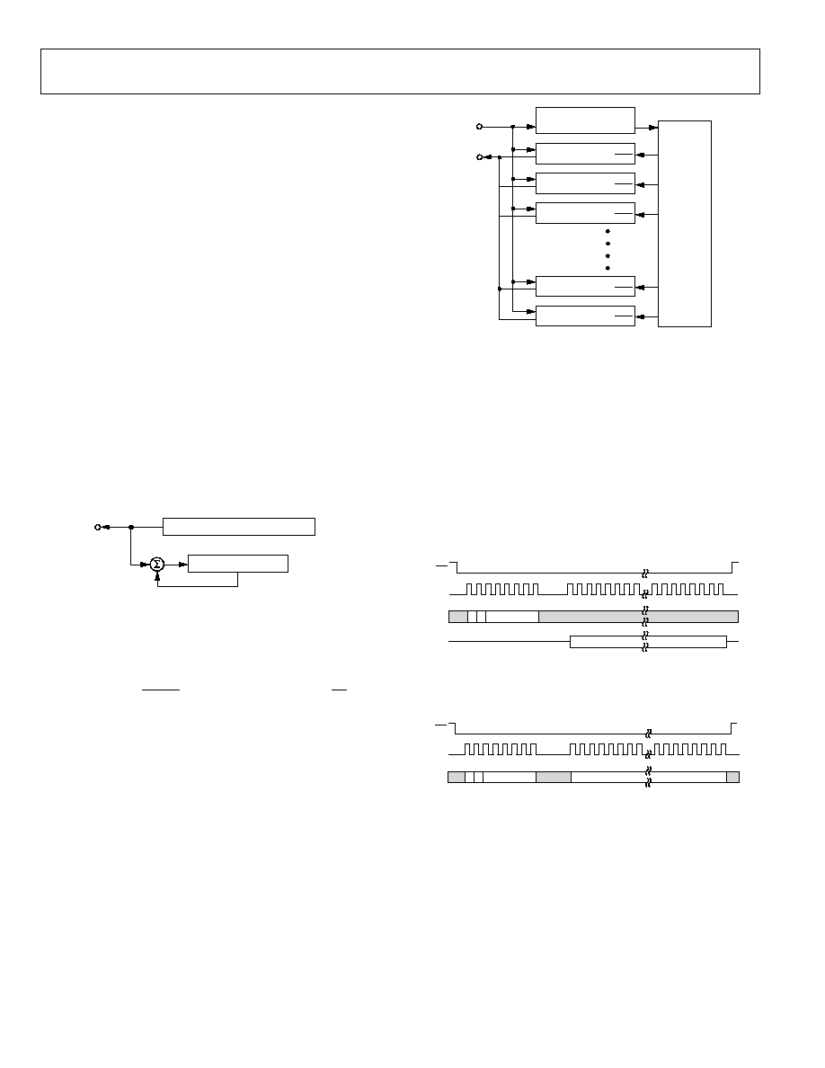
ADE7763
Rev. A | Page 44 of 56
SUSPENDING FUNCTIONALITY
The analog and the digital circuit can be suspended separately.
The analog portion can be suspended by setting the ASUSPEND
bit (Bit 4) of the mode register to logic high--see the Mode
Register (0x09) section. In suspend mode, all waveform samples
from the ADCs are set to 0s. The digital circuitry can be halted
by stopping the CLKIN input and maintaining a logic high or
low on the CLKIN pin. The ADE7763 can be reactivated by
restoring the CLKIN input and setting the ASUSPEND bit to
logic low.
CHECKSUM REGISTER
The ADE7763 has a checksum register (CHECKSUM[5:0]) to
ensure that the data bits received in the last serial read operation
are not corrupted. The 6-bit checksum register is reset before
the first bit (MSB of the register to be read) is put on the DOUT
pin. During a serial read operation, when each data bit becomes
available upon the rising edge of SCLK, the bit is added to the
checksum register. At the end of the serial read operation, the
content of the checksum register is equal to the sum of all ones
previously read in the register. Using the checksum register, the
user can determine if an error has occurred during the last read
operation. Note that a read to the checksum register also
generates a checksum of the checksum register itself.
CONTENT OF REGISTER (n-bytes)
CHECKSUM REGISTER ADDR: 0x3E
+
+
DOUT
04481-A
-
070
Figure 79. Checksum Register for Serial Interface Read
SERIAL INTERFACE
All ADE7763 functionality is accessible via several on-chip
registers--see Figure 80. The contents of these registers can be
updated or read using the on-chip serial interface. After power-
on or toggling the RESET pin low and a falling edge on CS, the
ADE7763 is placed in communication mode. In co
tion mode, the ADE7763 expects a write to its communication
to the communication register
mmunica-
register. The data written
determines whether the next data transfer operation is a read or
a write and which register is accessed. Therefore, all data
transfer operations with the ADE7763, whether a read or a
write, must begin with a write to the communication register.
COMMUNICATION
REGISTER
IN
OUT
IN
OUT
IN
OUT
IN
OUT
IN
OUT
REGISTER 1
REGISTER 2
REGISTER 3
REGISTER n1
REGISTER n
REGISTER
ADDRESS
DECODE
DIN
DOUT
04481-A
-
071
Figure 80. Addressing ADE7763 Registers via the Communication Register
The communication register is an 8-bit-wide register. The MSB
determines whether the next data transfer operation is a read or
a write. The 6 LSBs contain the address of the register to be
accessed--see the Communication Register section for a more
detailed description.
Figure 81 and Figure 82 show the data transfer sequences for a
read and write operation, respectively. Upon completion of a
data transfer (read or write), the ADE7763 again enters the
communication mode. A data transfer is complete when the
LSB of the ADE7763 register being addressed (for a write or a
read) is transferred to or from the ADE7763.
MULTIBYTE
COMMUNICATION REGISTER WRITE
DIN
SCLK
CS
DOUT
READ DATA
ADDRESS
0
0
04481-
A-
072
Figure 81. Reading Data from the ADE7763 via the Serial Interface
COMMUNICATION REGISTER WRITE
DIN
SCLK
ADDRESS
0
1
CS
0
4
4
8
1
-
073
MULTIBYTE READ DATA
Figure 82. Writing Data to the ADE7763 via the Serial Interface
A-
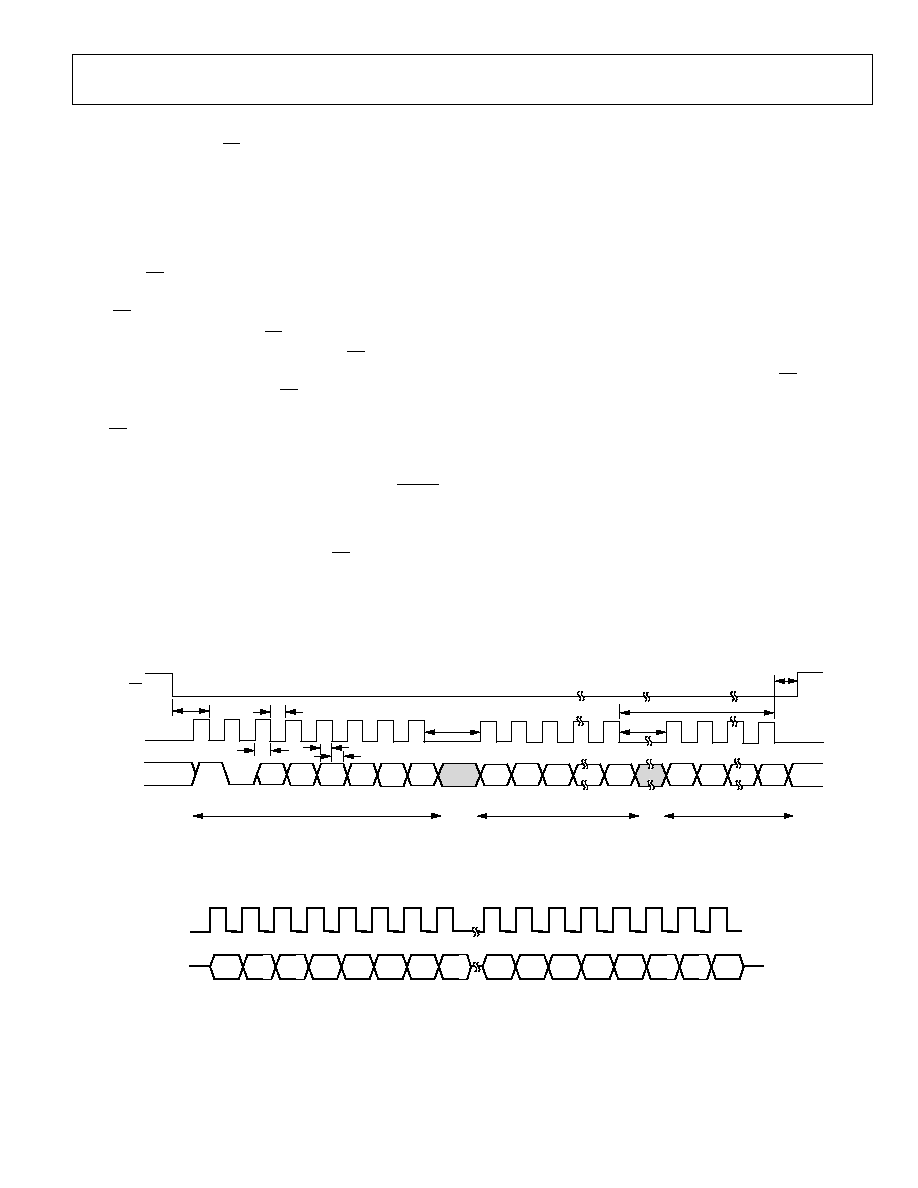
ADE7763
Rev. A | Page 45 of 56
ade up of four signals:
The serial interface of the ADE7763 is m
SCLK, DIN, DOUT, and CS. The serial clock for a data transfer
is applied at the SCLK logic input. This logic input has a Schmitt-
trigger input structure that allows slow rising and falling clo
edges to be used. All data transfer operations are synchronized
to the serial clock. Data is shifted into the ADE7763 at the DIN
logic input upon the falling edge of SCLK. Data is shifted out o
the ADE7763 at the DOUT logic output upon a rising edge o
SCLK. The
ck
f
f
CS logic input is the chip-select input. This input is
used when
multiple devices share the serial bus. A falling edge
upon CS also resets the serial in
into communication mode. T
terface and places the ADE7763
he CS input should be driven low
for the entire data transfer operation. Bringing CS high during a
data transfer operation aborts the transfer and places the serial
bus in a high impedance state. The CS logic input can be tied
low if the ADE7763 is the only device on the serial bus. However,
with CS tied low, all initiated data transfer operations must be
fully completed, i.e., the LSB of each register must be transferred
because there is no other way to bring the ADE7763 into commu-
nication mode without resetting the entire device using RESET.
ADE7763 Serial Write Operation
The serial write sequence takes place as follows. With the
ADE7763 in communication mode (i.e., the CS input logic low),
first a write to the communication register occurs. The MSB of
this byte transfer is a 1, indicating that the data transfer
operation is a write. The LSBs of this byte contain the address of
the register to be written to. The ADE7763 starts shifting in the
register data upon the next falling edge of SCLK. All remaining
bits of register data are shifted in upon the falling edge of
subsequent SCLK pulses--see Figure 83. As explained earlier,
the data write is initiated by a write to the communication
register followed by the data. During a data write operation,
data is transferred to all on-chip registers one byte at a time.
After a byte is transferred into the serial port, there is a finite
time before it is transferred to one of the ADE7763 on-chip
registers. Although another byte transfer to the serial port can
start while the previous byte is being transferred to an on-chip
register, this second byte transfer should not finish until at least
4 µs after the end of the previous byte transfer. This functionality
is expressed in the timing specification t
6
--see Figure 83. I
w
f a
rite operation is aborted during a byte transfer (CS is brought
high), then that byte cannot be written to the destination register.
Destination registers can be up to 3 bytes wide--see Table 9,
Table 10, Table 11, Table 12, and Table 13. Therefore the first
byte shifted into the serial port at DIN is transferred to the MSB
(most significant byte) o
f the destination register. If, for example,
3
the addressed register is 12 bits wide, a 2-byte data transfer
must take place. Because the data is always assumed to be right
justified, in this case the 4 MSBs of the first byte would be
ignored and the 4 LSBs of the first byte written to the ADE776
would be the 4 MSBs of the 12-bit word. Figure 84 illustrates
this example.
DIN
SCLK
t
2
t
3
t
4
t
5
COMMAND BYTE
1
0
A4
A5
A3
A2
A1
A0
CS
t
1
t
7
t
6
t
8
MOST SIGNIFICANT BYTE
LEAST SIGNIFICANT BYTE
DB7
DB0
DB7
DB0
t
7
04481-A
-
074
Interface Write Timing
Figure 83. Serial
SCLK
DIN
X
X
X
X
DB11 DB10
DB9
DB8
DB7
DB6
DB5
DB4
DB3
DB2
DB1
DB0
MOST SIGNIFICANT BYTE
LEAST SIGNIFICANT BYTE
04481-A
-
075
Figure 84. 12-Bit Serial Write Operation
ADE7763
Rev. A | Page 46 of 56
Serial Read Operation
During a data read operation from the ADE7763, data is shifted
out at the DOUT logic output upon the rising edge of SCLK. As
is the case with the data write operation, a write to the commu-
nication register must precede a data read.
With the ADE7763 in communication mode (CS logic low),
first an 8-bit write to the communication register occurs. The
MSB of this byte transfer is a 0, indicating that the next data
transfer operation is a read. The LSBs of this byte contain the
address of the register that is to be read. The ADE7763 starts
shifting data out of the register upon the next rising edge of
SCLK--see Figure 85. At this point, the DOUT logic output
leaves its high impedance state and starts driving the data bus.
All remaining bits of register data are shifted out upon subse-
quent SCLK rising edges. The serial interface also enters commu-
nication mode as soon as the read is complete. Then, the DOUT
logic output enters a high impedance state upon the falling edge
of the last SCLK pulse. The read operation can be aborted by
bringing the CS logic input high before the data transfer is
complete. The DOUT output enters a high impedance state
upon the rising edge of
CS.
When an ADE7763 register is addressed for a read operation,
the entire contents of that register are transferred to the serial
port. This allows the ADE7763 to modify its on-chip register
without the risk of corrupting data during a multibyte transfer.
Note that when a read operation follows a write operation, the
read command (i.e., write to communication register) should
not happen for at least 4 µs after the end of the write operation.
If the read command is sent within 4 µs of the write operation,
the last byte of the write operation could be lost. This timing
constraint is given as timing specification t
s
9
.
SCLK
CS
t
1
t
10
t
13
DB0
DB7
DB0
DB7
t
11
11
0
0
A4
A5
A3
A2
A1
A0
DIN
DOUT
t
t
12
COMMAND BYTE
MOST SIGNIFICANT BYTE
LEAST SIGNIFICANT BYTE
t
9
04481-A
-
076
Figure 85. Serial Interface Read Timing

ADE7763
Rev. A | Page 47 of 56
Descr
REGISTERS
Table 9. Summary of Registers by Address
Address Name
R/W No.
Bits Default Type
1
iption
0x01 WAVEFORM
R 24
0x0 S Wavef
wavef
1, Channel 2, or the active power
signal.
selecte
Sampl
orm Register. This read-only register contains the sampled
orm data from either Channel
The data source and the length of the waveform registers are
d by Bits 14 and 13 in the mode register--see the Channel 1
ing and Channel 2 Sampling sections.
0x02 AENERGY
R 24
0x0 S Active
time in
section.
Energy Register. Active power is accumulated (integrated) over
this 24-bit, read-only register--see the Energy Calculation
0x03 RAENERGY
R 24
0x0 S Same a
follow
s the active energy register, except that the register is reset to 0
ing a read operation.
0x04 LAENERGY
R 24
0x0 S Line A
power
numbe
ccumulation Active Energy Register. The instantaneous active
is accumulated in this read-only register over the LINECYC
r of half line cycles.
0x05 VAENERGY
R 24
0x0 U Appar
ulated over time in
this read-only re
ent Energy Register. Apparent power is accum
gister.
0x06 RVAENERGY
R 24
0x0 U Same as the VAENERGY register, except that the register is reset to 0
following a read operation.
0x07 LVAENERGY
R 24
0x0 U Line Accumulation Apparent Energy Register. The instantaneous real
power is accumulated in this read-only register over the LINECYC
number of half line cycles.
0x08 RESERVED
0x09 MODE R/W
16
0x000C
U Mode Register. This is a 16-bit register through which most of the
ADE7763's functionality is accessed. Signal sample rates, filter enabling,
and calibration modes are selected by writing to this register. The
contents can be read at any time--see the Mode Register (0X09) section.
0x0A IRQEN
R/W
16
0x40 U Interrupt Enable Register. ADE7763 interrupts can be deactivated at any
time by setting the corresponding bit in this 16-bit enable register to
Logic 0. The status register continues to detect an interrupt event even if
disabled; however, the IRQ output is not activated--see the Interru ts
p
section.
0x0B STATUS R 16
0x0
bit read-only register that contains
information regarding the source of ADE7763 interrupts--see the
Interrupts section.
U Interrupt Status Register. This is a 16-
0x0C RSTSTATUS
R 16
0x0 U Same as the interrupt status register, except that the register contents
are reset to 0 (all flags cleared) after a read operation.
0x0D CH1OS R/W
8
0x00 S
*
Channel 1 Offset Adjust. Bit 6 is not used. Writing to Bits 0 to 5 allows
offsets on Channel 1 to be removed--see the Analog Inputs and CH1OS
Register sections. Writing Logic 1 to the MSB of this register enables the
digital integrator on Channel 1; writing Logic 0 disables the integrator.
The default value of this bit is 0.
0x0E CH2OS R/W
8
0x0 S
*
Channel 2 Offset Adjust. Bits 6 and 7 are not used. Writing to Bits 0 to 5 of
this register allows offsets on Channel 2 to be removed--see the Analog
Inputs section. Note that the CH2OS register is inverted. To apply a
positive offset, a negative number is written to this register.
0x0F GAIN
R/W
8
0x0 U PGA Gain Adjust. This 8-bit register is used to adjust the gain selection for
the PGA in Channels 1 and 2--see the Analog Inputs section.
0x10 PHCAL R/W
6
0x0D S Phase Calibration Register. The phase relationship between Channel 1
and 2 can be adjusted by writing to this 6-bit register. The valid content
of this twos complement register is between 0x1D to 0x21. At the line
frequency of 60 Hz, this ranges from 2.06° to +0.7°--see the Phase
Compensation section.
0x11 APOS
R/W
16
0x0 S Active Power Offset Correction. This 16-bit register allows small offsets in
the active power calculation to be removed--see the Active Power
Calculation section.

ADE7763
Rev. A | Page 48 of 56
R/W No.
Bits Default Type
1
Description
Address Name
0x12 WGAIN R/W
12
0x0 S Power Gain Adjust. This is a 12-bit register. Calibrate the active power
calculation by writing to this register. The calibration range is ±50% of
ll-scale active power. The resolution of the gain adjust is
the nominal fu
0.0244%/LSB --see the Calibrating an Energy Meter section.
0x13 WDIV
R/W
8
0x0 U
GY
Active Energy Divider Register. The internal active energy register is
divided by the value of this register before being stored in the AENER
register.
0x14 CFNUM R/W
12
0x3F U
just the output frequency
CF Frequency Divider Numerator Register. Ad
on the CF pin by writing to this 12-bit read/write register--see the
Energy-to-Frequency Conversion section.
0x15 CFDEN R/W
12
0x3F U
ency Divider Denominator Register. Adjust the output
e
nversion section.
CF Frequ
frequency on the CF pin by writing to this 12-bit read/write register--se
the Energy-to-Frequency Co
0x16
IRMS
R
24
0x0
U
Channel 1 RMS Value (Current Channel).
0x17
VRMS
R
24
0x0
U
Channel 2 RMS Value (Voltage Channel).
0x18 IRMSOS R/W
12
0x0 S
ction Register.
Channel
1
RMS Offset Corre
0x19 VRMSOS R/W
12
0x0 S Channel
2
RMS Offset Correction Register.
0x1A VAGAIN R/W
12
0x0 S Apparent Gain Register. Calibrate the apparent power calculation by
writing to this register. The calibration range is 50% of the nominal
scale real power. The resolut
full-
ion of the gain adjust is 0.02444%/LSB.
0x1B VADIV R/W
er
8
0x0 U Apparent Energy Divider Register. The internal apparent energy regist
is divided by the value of this register before being stored in the
VAENERGY register.
0x1C LINECYC R/W
xFFFF
U
Line-Cycle Register. This 16-bit
et the
16
0
Line Cycle Energy Accumulation Mode
register is used during line cycle energy accumulation mode to s
number of half line cycles for energy accumulation--see the Line Cycle
Energy Accumulation Mode section.
0x1D ZXTOUT R/W
12
0xFFF U
e
Zero-Crossing Timeout. If no zero crossings are detected on Channel 2
within the time specified in this 12-bit register, the interrupt request lin
(IRQ) will be activated--see the Zero-Crossing Detection section.
0x1E SAGCYC R/W
8
0xFF U
e SAG output is activated--see the Line Voltage Sag Detection
Sag Line Cycle Register. This 8-bit register specifies the number of
consecutive line cycles below SAGLVL that is required on Channel 2
before th
section.
0x1F SAGLVL R/W
8
0x0 U
peak
nel 2 the SAG
Sag Voltage Level. An 8-bit write to this register determines at what
signal level on Chan
pin becomes active. The signal must
remain low for the number of cycles specified in the SAGCYC register
before the SAG pin is activated--see the Line Voltage Sag Detection
section.
0x20 IPKLVL R/W
8
0xFF U Channel 1 Peak Level Threshold (Current Channel). This register sets the
level of current peak detection. If the Channel 1 input exceeds this level,
the PKI flag in the status register is set.
0x21 VPKLVL R/W
8
0xFF U Channel 2 Peak Level Threshold (Voltage Channel). This register sets the
level of voltage peak detection. If the Channel 2 input exceeds this level,
the PKV flag in the status register is set.
0x22 IPEAK
R 24
0x0 U Channel 1 Peak Register. The maximum input value of the current
channel, since the last read of the register is stored in this register.
0x23 RSTIPEAK
R 24
0x0 U Same as Channel 1 peak register, except that the register contents are
reset to 0 after a read.
0x24 VPEAK R 24
0x0 U Channel 2 Peak Register. The maximum input value of the voltage
channel, since the last read of the register is stored in this register.
0x25 RSTVPEAK
R 24
0x0 U
e
Same as Channel 2 peak register, except that the register contents ar
reset to 0 after a read.
0x26 TEMP
R 8
0x0 S Temperature Register. This is an 8-bit register that contains the result of
the latest temperature conversion--see the Temperature Measurement
section.

ADE7763
Rev. A | Page 49 of 56
Address Name
R/W No.
Bits Default Type
1
Description
0x27 PERIOD R 16
0x0 U Period of the Channel 2 (Voltage Channel) Input Estimated by Zero-
Crossing Processing. The MSB of this register is always zero.
0x28
0x3C
Reserved.
0x3D
TMODE
R/W
8
U
Test Mode Register.
0x3E CHKSUM R 6
0x0 U
in the previous reads--see the Serial Read Operation section.
Checksum Register. This 6-bit, read-only register is equal to the sum of all
the ones
0x3F DIEREV R 8
U Die Revision Register. This 8-bit, read-only register contains the revision
number of the silicon.
1
Type decoder: U = unsigned, S = signed by twos complement method, and S
*
= signed by sign magnitude method.

ADE7763
Rev. A | Page 50 of 56
REGISTER DESCRIPTIONS
All ADE7763 functionality is accessed via on-chip registers. Each r
ister and
ansf ring the regis
data. full descr tion of the se
l int
col is given in the Serial Interface section.
MU
N R
T
omm
egis
is an
bit, write
regist
at con
processor. All data transfer operations must begin with a write to t
r det
wheth
the n t operation is a read o
write
designations for the communication register.
DB7 DB6 DB5 DB4 DB3 DB2 DB1 DB0
egister is accessed by first writing to the communication reg
then tr
er
ter
A
ip
ria
erface proto
COM
NICATIO
EGIS ER
The c
unication r
ter
8-
-only
er th
trols the serial data transfer between the ADE7763 and the host
he communication register. The data written to the communication
registe
ermines
er
ex
r a
and which register is being accessed. Table 10 outlines the bit
W/R
0 A5 A4 A3 A2 A1 A0
Table 10. Communication Register
Bit
Location
Bit
Mnemonic Description
0 to 5
A0 to A5
The 6 LSBs of the communication register specify the register for the data transfer operation. Table 9 lists the
address of each on-chip register.
6
RESERVED
This bit is unused and should be set to 0.
7 W/R
When this bit is a Logic 1, the data transfer operation immediately following the write to the communication
register is interpreted as a write to the ADE7763. When this bit is a Logic 0, the data transfer operation
immediately following the write to the communication register is interpreted as a read operation.
MODE REGISTER (0x09)
The ADE7763 functionality is configured by writing to the mode register. Table 11 describes the functionality of each bit
in the register.
Table 11.
Bit
Location
Bit
Mnemonic
Default
Value Description
0
DISHPF
0
HPF (high-pass filter) in Channel 1 is disabled when this bit is set.
1
DISLPF2
0
LPF (low-pass filter) after the multiplier (LPF2) is disabled when this bit is set.
2
DISCF
1
Frequency output CF is disabled when this bit is set.
3
DISSAG
1
Line voltage sag detection is disabled when this bit is set.
4 ASUSPEND
0 By setting this bit to Logic 1, both A/D converters can be turned off. During normal operation, this
bit should be left at Logic 0. All digital functionality can be stopped by suspending the clock
signal at CLKIN pin.
5 TEMPSEL
0 Temperature conversion starts when this bit is set to 1. This bit is automatically reset to 0 after the
temperature conversion.
6 SWRST
0 Software Chip Reset. A data transfer should not take place to the ADE7763 for at least 18 µs after
a software reset.
7
CYCMODE
0
Setting this bit to Logic 1 places the chip in line cycle energy accumulation mode.
8
DISCH1
0
ADC 1 (Channel 1) inputs are internally shorted together.
9
DISCH2
0
ADC 2 (Channel 2) inputs are internally shorted together.
10 SWAP
0 By setting this bit to Logic 1, the analog inputs V2P and V2N are connected to ADC 1 and the
analog inputs V1P and V1N are connected to ADC 2.
Use these bits to select the waveform register update rate.
DTRT1
DTRT0
Update
Rate
0
0
27.9 kSPS (CLKIN/128)
0
1
14 kSPS (CLKIN/256)
1
0
7 kSPS (CLKIN/512)
12, 11
DTRT1, 0
00
1
1
3.5 kSPS (CLKIN/1024)
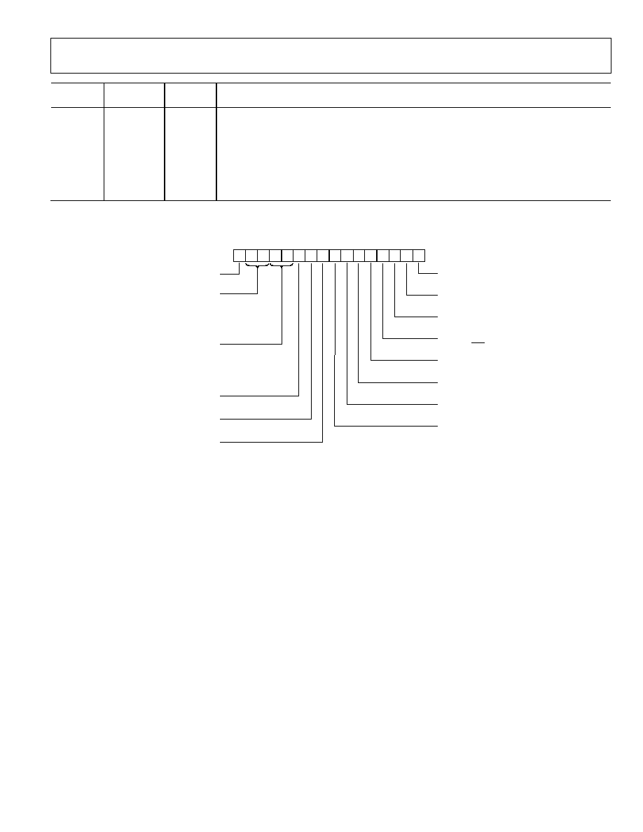
ADE7763
Rev. A | Page 51 of 56
Description
Bit
Location
Bit
Mnemonic
Default
Value
Use these bits to select the source of the sampled data for the waveform register.
WAVSEL1, 0
Length
Source
14, 13
WAVSEL1, 0
00
0
0
24 bits, active power signal (output of LPF2)
0 1
Reserved
1
0
24 bits, Channel 1
1
1
24 bits, Channel 2
15
POAM
0
Writing Logic 1 to this bit allows only positive power to accumulate. The default value of this bit is 0.
UTP
27.9k
01 = 14.4k
10 = 7.2k
11 = 3.6kS
POAM
SEL
(WAVEFORM SELECTION FOR SAMPLE MODE)
0
0
0
0
0
0
0
0
0
0
1
1
SWAP
(SWAP CH1 AND CH2 ADCs)
DTRT
(WAVEFORM SAMPLES O
00 =
UT DATA RATE)
SPS (CLKIN/128)
SPS (CLKIN/256)
SPS (CLKIN/512)
PS (CLKIN/1024)
(POSITIVE ONLY ACCUMULATION)
WAV
00 = LPF2
01 = RESERVED
10 = CH1
11 = CH2
0
0
0
0
15 14 13
1 10 9
8
5
4
3
2
ADDR: 0x09
12 1
7
6
1
0
DISHPF
(DISABLE HPF1 IN CHANNEL 1)
DISLPF2
(DISABLE LPF2 AFTER MULTIPLIER)
DISCF
DISSAG
(DISABLE SAG OUTPUT)
SWRST
(SOFTWARE CHIP RESET)
CYCMODE
ATION MODE)
DISCH2
CHANNEL 2)
(DISABLE FREQUENCY OUTPUT CF)
ASUSPEND
(SUSPEND CH1 AND CH2 ADCs)
TEMPSEL
(START TEMPERATURE SENSING)
(LINE CYCLE ENERGY ACCUMUL
NOTE: REGISTER CONTENTS SHOW POWER-ON DEFAULTS
04481-A
-
077
Figure 86. Mode Register
(SHORT THE ANALOG INPUTS ON
DISCH1
(SHORT THE ANALOG INPUTS ON CHANNEL 1)
ADE7763
Rev. A | Page 52 of 56
P
R
(0
T
TA
EGI
,
RUP
R
STER (0
The status register is used by the MCU to
source of a
upt requ
INTERRU
RESET IN
T STATUS
ERRUPT S
EGISTER
TUS R
x0B),
STER (0x0C)
INTER
T ENABLE EGI
x0A)
determine the
n interr
est (IRQ). When an interrupt event occurs, the
corresponding flag in the interrupt status
gister is set to logic hig
f the enable bi
g is Logic 1 in the interrupt enable register,
the IRQ
re
h. I
t for this fla
logic output will go active low. W
the MCU services th
terrupt, it mu
read from the interrupt status
register to determine the source of the int
upt.
able 12.
Bit
Location
Interrupt
Flag
Description
hen
e in
st first carry out a
err
T
0
AEHF
Indicates that an interrupt occurred because the active energy register, AENERGY, is more than half full.
1
SAG
Indicates that an interrupt was caused by a sag on the line voltage.
2 CYCEND
Indicates the end of energy accumulation over an integral number of half line cycles, as defined by the content
of the LINECYC register--see the Line Cycle Energy Accumulation Mode section.
3
WSMP
Indicates that new data is present in the waveform register.
4
ZX
This status bit reflects the status of the ZX logic ouput--see the Zero-Crossing Detection section.
5
TEMP
Indicates that a temperature conversion result is available in the temperature register.
6 RESET
Indicates the end of a reset for software and hardware resets. The corresponding enable bit has no function in
the interrupt enable register, i.e., this status bit is set at the end of a reset, but cannot be enabled to cause an
interrupt.
7
AEOF
Indicates that the active energy register has overflowed.
8
PKV
Indicates that the waveform sample from Channel 2 has exceeded the VPKLVL value.
9
PKI
Indicates that the waveform sample from Channel 1 has exceeded the IPKLVL value.
10
VAEHF
Indicates that an interrupt occurred because the apparent energy register, VAENERGY, is more than half full.
11
VAEOF
Indicates that the apparent energy register has overflowed.
12 ZXTO
Indicates that an interrupt was caused by a missing zero crossing on the line voltage for a specified number of
line cycles--see the Zero-Crossing Timeout section.
13
PPOS
Indicates that the power has gone from negative to positive.
14
PNEG
Indicates that the power has gone from positive to negative.
15 RESERVED
Reserved.
VAEHF
(VAENERGY IS HALF FULL)
PPOS
(POWER NEGATIVE TO POSITIVE)
RESERVED
PNEG
(POWER POSITIVE TO NEGATIVE)
0
0
0
0
0
0
0
0
0
0
0
0
0
0
0
0
8
9
7
4
5
6
2
3
0
1
15 14 13 12 11 10
AEHF
(ACTIVE ENERGY HALF FULL)
SAG
(SAG ONLINE VOLTAGE)
CYCEND
(END OF LINECYC HALF LINE CYCLES)
WSMP
(WAVEFORM SAMPLES DATA READY)
ZX
(ZERO CROSSING)
TEMP
(TEMPERATURE DATA READY)
RESET
(END OF SOFTWARE/HARDWARE RESET)
AEOF
(ACTIVE ENERGY REGISTER OVERFLOW)
ZXTO
(ZERO-CROSSING TIMEOUT)
VAEOF
(VAENERGY OVERFLOW)
PKI
(CHANNEL 1 SAMPLE ABOVE IPKLVL)
PKV
(CHANNEL 2 SAMPLE ABOVE VPKLVL)
04481-A
-
079
ADDR: 0x0A, 0x0B, 0x0C
Figure 87. Interrupt Status/Interrupt Enable Register
ADE7763
Rev. A | Page 53 of 56
r. The MSB of this register is used to switch the digital integrator on and off in
offset correction in Channel 1. Table 13 summarizes the function of this register.
CH1OS REGISTER (0x0D)
The CH1OS register is an 8-bit, read/write enabled registe
Channel 1, and Bits 0 to 5 indicate the amount of
Table 13. CH1OS Register
Bit
Location
Bit
Mnemonic
Description
0 to 5
OFFSET
The 6 LSBs of the CH1OS register control the amount of dc offset correction in the Channel 1 ADC. The 6-bit
offset correction is sign and magnitude coded. Bits 0 to 4 indicate the magnitude of the offset correction.
Bit 5 shows the sign of the offset correction. A 0 in Bit 5 means the offset correction is positive, and a 1
indicates the offset correction is negative.
6
Not Used
t used.
This bit is no
7 INTEGRATOR
tting
This bit is used to activate the digital integrator on Channel 1. The digital integrator is switched on by se
this bit. This bit is set to 0 by default.
DIGITAL INTEGRATOR SELECTION
1 = ENABLE
0 = DISABLE
NOT USED
0
0
0
0
0
0
0
0
7
6
5
4
3
2
1
0
ADDR: 0x0D
SIGN AND MAGNITUDE CODED
OFFSET CORRECTION BITS
04481-A
-
078
Figure 88. Channel 1 Offset Register
ADE7763
Rev. A | Page 54 of 56
S
OUTLINE DIMENSION
20
11
7.50
7.20
6.90
8.20
7.80
7.40
5.60
5.30
5.00
10
1
COPLANARITY
0.10
0.05 MIN
1.85
1.75
1.65
0.65
BSC
0.25
0.09
0.95
0.75
0.55
8°
4°
0°
2.00 MAX
0.38
0.22 SEATING
PLANE
PIN 1
COMPLIANT TO JEDEC STANDARDS MO-150AE
Figure 89. 20-Lead Shrink Small Outline Package [SSOP]
(RS-20)
Dimensions shown in millimeters
ORDERING GUIDE
Model
Temperature Range
Package Description
Package Option
ADE7763ARS
-40°C to +85°C
20-Lead SSOP
RS-20
ADE7763ARSRL
-40°C to +85°C
20-Lead SSOP
RS-20
EVAL-ADE7763EB
Evaluation
Board

ADE7763
Rev. A | Page 55 of 56
NOTES

ADE7763
Rev. A | Page 56 of 56
© 2004 Analog Devices, Inc. All rights reserved. Trademarks and
registered trademarks are the property of their respective owners.
D04481010/04(A)
NOTES
Document Outline