Äîêóìåíòàöèÿ è îïèñàíèÿ www.docs.chipfind.ru

=
EVAL-ADF4208EB1
FEATURES
Evaluation Board featuring the ADF4208 synthesiser.
Requires only RF and IF VCO's and Loop Filters for dual
PLL.
Complete with SMA connectors, battery, and on board
10MHz Crystal.
Programmable via a serial interface.
Accompanying Software allows complete control of synthesizer
functions from PC using Windows 95/98/NT
Battery Operated: Choice of 3V or 5V supplies
On Board Monitoring of Current and Voltage.
© Analog Devices, Inc., 1999
One Technology Way, P.O. Box 9106, Norwood, MA 02062-9106, U.S.A.
Tel: 781-329-4700
Fax: 781-326-8703
Information furnished by Analog Devices is believed to be accurate and reliable. However,
no responsibility is assumed by Analog Devices for its use, nor for any infringements of
patents or other rights of third parties which may result from its use. No license is granted
by implication or otherwise under any patent or patent rights of Analog Devices.
Evaluation Board For PLL Frequency
Synthesizer
BLOCK DIAGRAM
REV.PrA 02/00
GENERAL DESCRIPTION
This board is designed to allow the user to evaluate
the performance of the ADF4208 Dual Frequency
Synthesizer for PLL's (Phase Locked Loops). The
block diagram of the board is shown below. It con-
tains the ADF4208 synthesizer, a pc connector, and
SMA connections for refererence input, power
supplies and RF and IF output. The board only
requires an RF VCO and loop filter and an IF VCO
and loop filter. A cable is included with the board to
connect to a pc printer port.
The package also contains windows software to allow
easy programming of the synthesizer.
V C O 1
P C C O N NE C TO R
9 V B A TTE R Y
A D F4 2 0 8
E V A L-A D F4 2 0 8E B 1
V
P
V C O 2
V TU N
R F
O U T
V
V C O
V
D D
N ot P op ula ted
1 0 M H z C ry s ta l
A D 77 06
S M A
S oc k e t
P O W E R S W ITCH
O N
O FF
P C C O N NE C TO R
9 V B A TTE R Y
N ot P op ula ted
R E F
IN
S M A
S oc k e t
IF
O U T
V C O 2
A D 77 06
V C O 1
V TU N
V C O 1
FO U T
V C O 2
FO U T
R S E T
EVAL-ADF4208EB1
REV.PrA 02/00
2
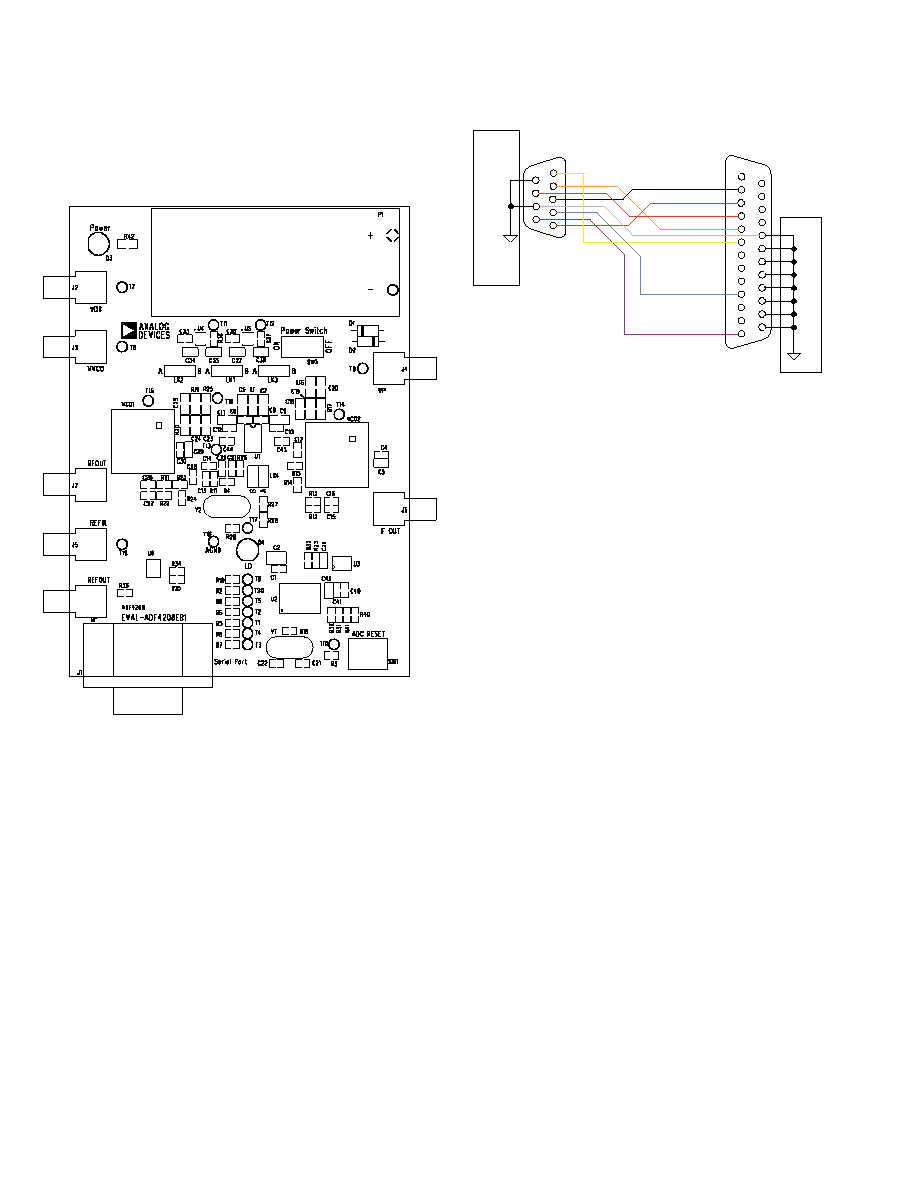
Figure 2. PC Cable Diagram
connectors. If the user wishes they may use their own
power supplies and use the reference output. In this case,
they need to insert SMA connectors to as shown on the
silkscreen and block diagram.
The AD7706 A/D converter is used to monitor the power
supply voltage and current consumption of the ADF4208.
This helps the user pick the optimum synthesizer settings for
power consumption and also provides an alert if the battery
voltage is too low to sustain the required 3V or 5V for the
board supply.
Hardware Description
The evaluation board comes with a cable for connecting to
the printer port of a PC. The silk screen and cable diagram for
the evaluation board are shown below. The board
schematic is shown on pages 3 and 4.
1
2
3
7
8
9
11
12
14
15
16
17
18
19
20
21
22
23
24
25
1
2
3
4
5
6
7
8
9
Black - CLK
Brown - DATA
Red - LE
Orange - CE
25 Way Male
D-Type
To
PC Printer Port
9 Way
Female D-Type
To
ADF411X
ADF421X
Evaluation
Board
PC
EVAL-ADF411X
EVAL-ADF421X
White - GND
6
4
5
Blue
Purple
Yellow
13
10
The board is powered from a single 9V battery. The
power supply ciruitry allows the user to choose either 3V
or 5V for the ADF4208 V
DD
and V
P
, and for the VCO
supply. The default settings are 3V for the ADF4208 V
DD
and 5V for the ADF4208 V
P
and for the VCO supply. It
is very important to note that the ADF4208 V
DD
should
never exceed the ADF4208 V
P
. This can damage the de-
vice.
All components necessary for LO generation are catered
for on-board. The crystal oscillator circuit provides the
necessary 10MHz reference frequency. The addition of an
SMA connector allows an external reference to be used
(Please consult circuit diagram to see what components
are needed to be added or removed for this). The PLL
requires a loop filter and VCO for both the IF and RF
sides to complete the dual PLL. The output is available
at RF OUT and IF OUT through standard SMA
Figure 1. Evaluation Board Silkscreen
EVAL-ADF4208EB1
3
REV.PrA 02/00
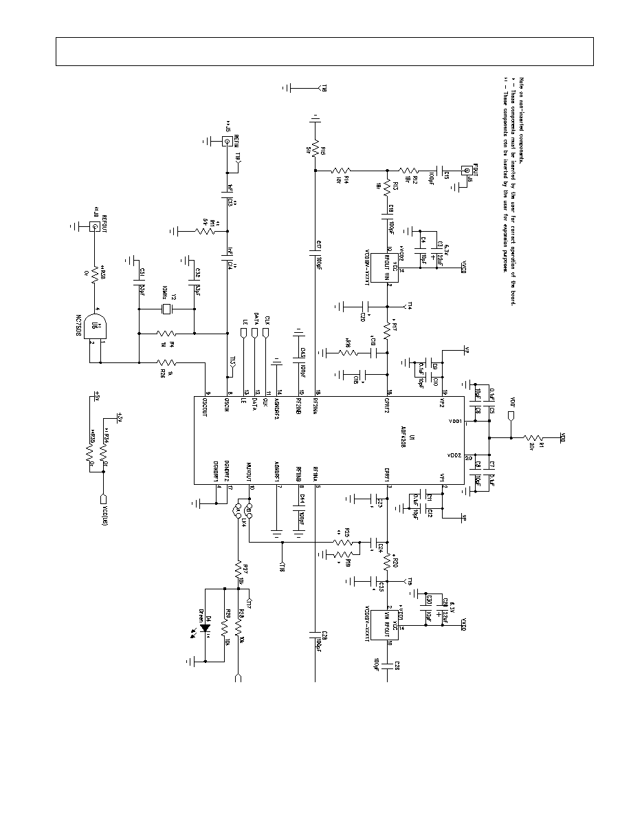
Figure 3. Evaluation Board Circuit Diagram (Page 1)
EVAL-ADF4208EB1
REV.PrA 02/00
4
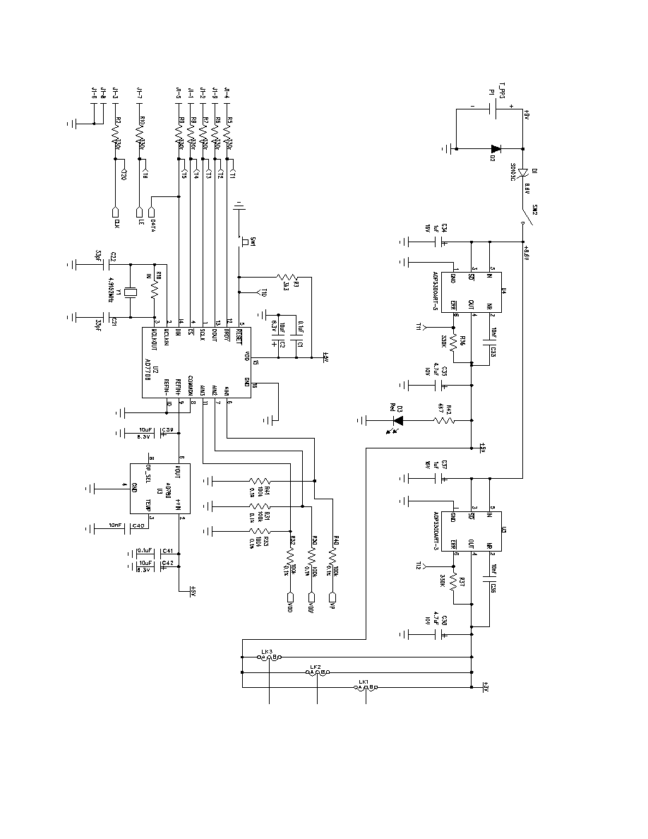
Figure 4. Evaluation Board Circuit Diagram (Page 2)
EVAL-ADF4208EB1
5
REV.PrA 02/00
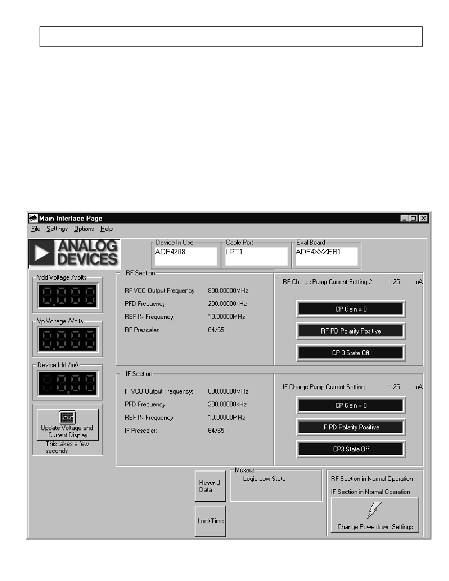
Figure 5. Software Front Panel
Software Description
The software comes on a CD. If the user runs
"ADF4XXXEvaluationSoftware.exe" on the CD, then the
install wizard installs the software. Follow the on-screen
directions. The software will be installed in a default
directory called "C:\Program Files\Analog
Devices\ADF4xxx Evaluation Software". To run the
software, simply double click on "ADF4XXX Eval
Software.exe".
The front panel of the evaluation board software is shown
below.
When the device window appears, choose the ADF4208
and click OK. The main software screen now appears.
Follow the steps below for initial setup to interface to the
part.
Click on Choose Port, and the Port Connector window
will appear. Choose the port that the cable is connected to
on the PC and click OK. (Normally LPT1)
Click on REF IN Frequency, and the REF IN Frequency
window will appear. Enter the reference frequency being
used and click OK. This will be 10MHz with the Crystal.
Click on RF VCO Output Frequency, and the Output
Frequency window will appear. Enter the output frequency
and PFD reference frequency, and click OK. Repeat this
for the IF side.
Click On Prescaler, and the Prescaler window will appear.
Grab the pointer, and choose the desired prescaler value.
Click OK.
Click on the RF PD Polarity button to set the RF PD Polarity
bit High.
Click on Charge Pump Current Setting 2 or Charge Pump
Current Setting 1 and the Current Setting window will ap-
pear. Grab the pointer to set the Charge Pump Current Set-
ting. Click OK.
The data is now set up, and other features can now be exam-
ined by the user.
EVAL-ADF4208EB1
REV.PrA 02/00
6
Table 1. Bill of Materials for the EVAL-ADF4208EB1
Qty
Re fe re nce
De scription
M a nufa ctu re r
P CB DECAL
V ALUE
1
U1
A DF4208B RU
A DI
TS S OP -20
A DF4208B RU
1
U2
A D7706B R
A DI
S O 16W B
A D7706B R
1
U3
A D780A R
A DI
S O 8NB
A D780A R
1
U4
A DP 3300A RT-5
A DI
S O T23-6
A DP 3300A RT-5
1
U5
A DP 3300A RT-3
A DI
S O T23-6
A DP 3300A RT-3
1
U6
Do Not Ins ert
Fairc hild
S O T23-5
NC7S M 508
1
V CO1
Do Not Ins ert
V ari-L
1
V CO2
Do Not Ins ert
V ari-L
1
Y 1
4.9152M Hz Cry s tal
V ec tron International
HC49 low profile
V XA 4-1011
1
Y 2
10M Hz Cry s tal
V ec tron International
HC49 low profile
V XA 4-1B 2-10M 00
1
D1
S D103C S c hottk y Diode
General S em ic onduc tor
DO 35
S D103C
1
D2
IN4001
D035
FE C 365-117
1
D3
Red Low P ower LE D
V is hay
LE D
FE C 657-130
1
D4
Green Low P ower LE D (Do Not Ins ert)
V is hay
LE D
FE C 657-141
6
C1 C5 C7 C9 C11 C41
M ulti Lay er Ceram ic Capac itor
M urata
Cas e 0603
0.1uF
1
C2
Tantalum Capac itor
A V X
CA P \TA J_B
10uF 6.3V
2
C3 C29
Tantalum Capac itor
A V X
CA P \TA J_A
22uF 6.3V
6
C4 C6 C8 C10 C12 C30
M ulti Lay er Ceram ic Capac itor
M urata
Cas e 0603
10pF
2
C13-14
Do Not Ins ert
M urata
Cas e 0603
1nF
8
C15-17 C26-28 C43-44
M ulti Lay er Ceram ic Capac itor
M urata
Cas e 0603
100pF
1
C18
Do Not Ins ert
M urata
Cas e 0805
1
C19
Do Not Ins ert
M urata
Cas e 0805
1
C20
Do Not Ins ert
M urata
Cas e 0805
4
C21-22 C31-32
M ulti Lay er Ceram ic Capac itor
M urata
Cas e 0603
33pF
1
C23
Do Not Ins ert
M urata
Cas e 0805
1
C24
Do Not Ins ert
M urata
Cas e 0805
1
C25
Do Not Ins ert
M urata
Cas e 0805
3
C33 C36 C40
M ulti Lay er Ceram ic Capac itor
M urata
Cas e 0603
10nF
2
C34 C37
Tantalum Capac itor
A V X
CA P \TA J_A
1uF 16V
2
C35 C38
Tantalum Capac itor
A V X
CA P \TA J_A
4.7uF 10V
2
C39 C42
Tantalum Capac itor
A V X
CA P \TA J_A
10uF 6.3V
1
R1
Res is tor (S urfac e M ount)
B ourns
Cas e 0805
20r 1.0%
7
R2 R5-10
Res is tor (S urfac e M ount)
B ourns
Cas e 0603
330r 1.0%
1
R3
Res is tor (S urfac e M ount)
B ourns
Cas e 0603
3k 3 1.0%
2
R4 R18
Res is tor (S urfac e M ount)
B ourns
Cas e 0603
1M 1.0%
1
R11
Do Not Ins ert
B ourns
Cas e 0603
51r 1.0%
6
R12-14 R21-23
Res is tor (S urfac e M ount)
B ourns
Cas e 0603
18r 1.0%
2
R15 R24
Res is tor (S urfac e M ount)
B ourns
Cas e 0603
51r 1.0%
1
R16
Do Not Ins ert
Cas e 0805
1
R17
Do Not Ins ert
Cas e 0805
1
R19
Do Not Ins ert
Cas e 0805
1
R20
Do Not Ins ert
Cas e 0805
1
R25
Do Not Ins ert
Cas e 0805
1
R26
Res is tor (S urfac e M ount)
B ourns
Cas e 0603
1k 1.0%
3
R27-29
Res is tor (S urfac e M ount)
B ourns
Cas e 0603
10k 1.0%
6
R30-33 R40-41
Res is tor (S urfac e M ount)
M eggitt
Cas e 0603
100k 0.1%
3
R34-35 R38
Do Not Ins ert
Cas e 0603
0r 1.0%
2
R36 R37
Res is tor (S urfac e M ount)
B ourns
Cas e 0603
330k 1.0%
1
R42
Res is tor (S urfac e M ount)
B ourns
Cas e 0603
4k 7 1.0%
1
S W 1
P us h B utton S witc h
Om ron
S W \P B -S M A LL
FE C 176-986
1
S W 2
S P DT S witc h - (W as hable)
A pem
S W _S IP -3P
FE C 150-559
20
T1-20
Red Tes tpoint
W Hughes
TE S TP OINT
FE C-240-345
1
J1
9 P IN D-TY P E M A LE (HORIZ)
M c M urdo
DCON9M
FE C 150-750
5
J2 J3 J4 J5 J8
Do Not Ins ert
S M A
2
J6 J7
GO LD 50
S M A S OCK E T
P as ternac k
S M A
P E 4118
3
LK 1 LK 2 LK 3
3 pin header
Harwin
S IP -3P
FE C 512-047
1
LK 4
4 pin header (2x 2)
Harwin
FE C 512-035
4
LK 1-4
S horting S hunt
Harwin
FE C 150-410
4
E ac h Corner
Rubber S tic k -O n Feet
3M
FE C 148-922
2
P 1
P air P CB s nap-on battery c onnec tor
K ey s tone
B A TT_P P 3
FE C 723-988
1
P 1
9V P P 3 B attery
Durac ell
FE C 908-526
1
P CB
E V A L-A DF 4208E B 1