a
EVAL-ADF4212EB1
FEATURES
Self Contained Evaluation Board including Synthesizer,
VCOs, Loop Filters for generating GSM 1800 standards
(1700MHz to 1800MHz RF, 520MHz to 560MHz IF).
RF and IF filters designed for 20kHz Loop Bandwidth, and
200kHz Channel Spacing.
Accompanying Software allows complete control of syn-
thesizer functions from PC using Windows 95/98/NT.
Battery Operated: Choice of 3V or 5V supplies
On-Board Monitoring of Voltage and Current
Typical RF Phase Noise Performance of -84dBc/Hz @1kHz
offset.
Typical IF Phase Noise Performance of -90dBc/Hz @1kHz
offset.
Typical Spurious Performance of batter than -80dBc
@200kHz offset.
© Analog Devices, Inc., 1999
One Technology Way, P.O. Box 9106, Norwood, MA 02062-9106, U.S.A.
Tel: 781-329-4700
Fax: 781-326-8703
Information furnished by Analog Devices is believed to be accurate and reliable. However,
no responsibility is assumed by Analog Devices for its use, nor for any infringements of
patents or other rights of third parties which may result from its use. No license is granted
by implication or otherwise under any patent or patent rights of Analog Devices.
Evaluation Board For PLL Frequency
Synthesizer
BLOCK DIAGRAM
REV 0 11/00
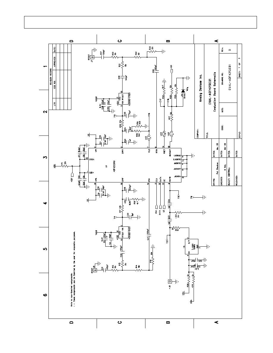
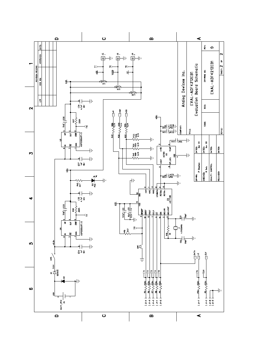
GENERAL DESCRIPTION
This board is designed to allow the user to evaluate
the performance of the ADF4212 Frequency Synthe-
sizer for PLL's (Phase Locked Loops). The block
diagram of the board is shown below. It contains the
footprint for a ADF4212 synthesizer, a pc connector,
SMA connector for the reference input, power sup-
plies and RF output. There is also a loop filter and a
VCO for both the RF and IF section on board. A
cable is included with the board to connect to a pc
printer port.
The package also contains Windows 95/98/NT soft-
ware to allow easy programming of the synthesizer.
VC O 1
(Vari-L)
VC O 1 90-XX XT
A DF42 1X
PC C O NNEC TO R
9V BA TTER Y
EV AL-AD F42 1XE B1
V
P
R EF
IN
R F
O U T
SM A
Soc ket
V
VC O
V
D D
TC XO
Ve ctron
A D7 706
PO W ER SW ITCH
O N
O FF
VC O 1
(Vari-L)
VC O 1 90-XX XT
IF
O U T
SM A
Soc ket
EVAL-ADF4212EB1
REV 0 11/00
2
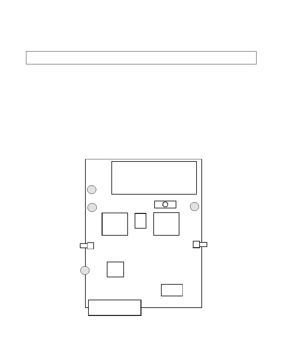
Figure 1. Evaluation Board Silkscreen
Figure 2. PC Cable Diagram
1
2
3
7
8
9
11
12
14
15
16
17
18
19
20
21
22
23
24
25
1
2
3
4
5
6
7
8
9
Black - CLK
Brown - DATA
Red - LE
Orange - CE
25 Way Male
D-Type
To
PC Printer Port
9 Way
Female D-Type
To
ADF411X
ADF421X
Evaluation
Board
PC
EVAL-ADF411X
EVAL-ADF421X
White - GND
6
4
5
Blue
Purple
Yellow
13
10
Hardware Description
The evaluation board comes with a cable for connecting to
the printer port of a PC. The silk screen and cable diagram for
the evaluation board are shown below. The board schematic is
shown on pages 3 and 4.
The board is powered from a single 9V battery. The
power supply ciruitry allows the user to choose either 3V
or 5V for the ADF4212 V
DD
and V
P
, and for the VCO
supply. The default settings are 3V for the ADF4212 V
DD
and 5V for the ADF4212 V
P
and for the VCO supply. It
is very important to note that the ADF4212 V
DD
should
never exceed the ADF4212 V
P
. This can damage the de-
vice.
All components necessary for LO generation are catered
for on-board. The TCXO connector provides the neces-
sary Reference Input. The RF PLL is made up of the
ADF4212, passive loop filter and the VCO 190-1750T
from Vari-L. The output is available at RFOUT through
a standard SMA connector. The IF PLL is made up of the
ADF4212, passive loop filter and the VCO 190-540T
from Vari-L. The output is available at IFOUT through
a standard SMA connector. If the user wishes they may
use their own power supplies and reference input. In this
case, they need to insert SMA connectors to as shown on
the silkscreen and block diagram.
The AD7706 A/D converter is used to monitor the power
supply voltage and current consumption of the ADF4212.
This helps the user pick the optimum synthesizer settings for
power consumption and also provides an alert if the battery
voltage is too low to sustain the required 3V or 5V for the
board supply.
EVAL-ADF4212EB1
5
REV 0 11/00
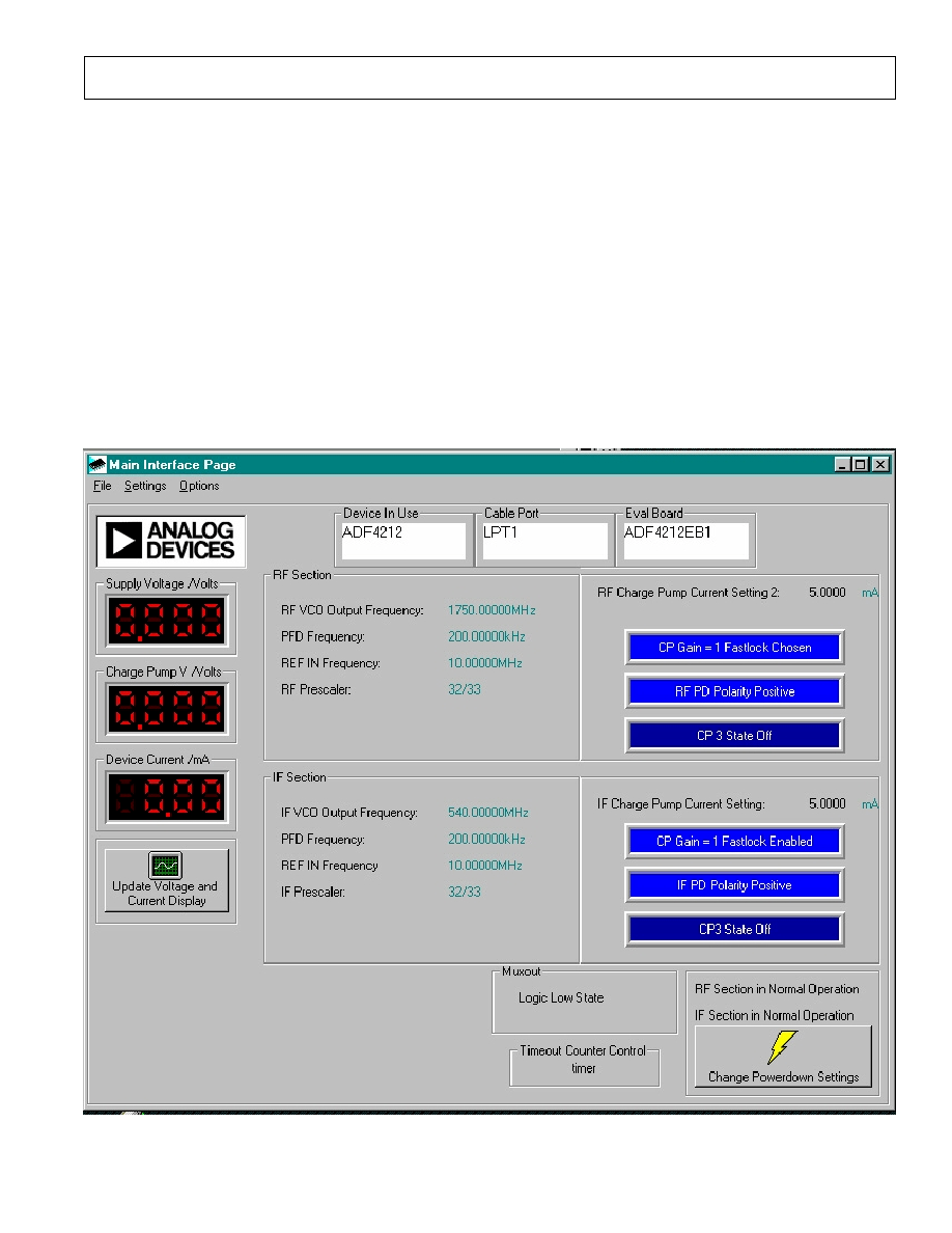
Figure 5. Software Front Panel
Software Description
The software comes on a CD. If the user double clicks on
"ADF4XXXEvaluationSoftware.exe" on the CD, then the
install wizard installs the software. Follow the on-screen
directions. The software will be installed in a default
directory called "C:\Program Files\Analog
Devices\ADF4xxx Evaluation Software". To run the
software, simply double-click on "ADF4XXX Eval
Software.exe".
The front panel of the evaluation board software is shown
below.
When the device window appears, choose ADF4212 and
click OK. The main software panel now appears. Click on
Eval Board in the top right hand side of the main software
screen. The Eval Board Window now appears. Click on
Eval-ADF4212EB1 and Click OK. This will set the cor-
rect data for the board configuartion. The device has now
been programmed and other features can now be exam-
ined by the user.