Äîêóìåíòàöèÿ è îïèñàíèÿ www.docs.chipfind.ru
=
EVAL-ADF4213EB1
FEATURES
Self-Contained Board including Synthesizer, VCO,s and
Loop Filter
Channel Spacing: 200kHz
RF Output:
900MHz
IF Output:
540MHz
Designed for 20kHz loop bandwidth on both IF and RF
Accompanying Software allows complete control of synthe-
sizer functions from PC
Battery Operated: Choice of 3V or 5V supplies
Typical Phase Noise Performance of -91dBc/Hz @ 1kHz
offset for RF (900MHz)
Typical Spurious Performance of better than -90dBc at
200kHz offset from carrier
© Analog Devices, Inc., 1999
One Technology Way, P.O. Box 9106, Norwood, MA 02062-9106, U.S.A.
Tel: 781-329-4700
Fax: 781-326-8703
Information furnished by Analog Devices is believed to be accurate and reliable.
However, no responsibility is assumed by Analog Devices for its use, nor for any
infringements of patents or other rights of third parties which may result from its use.
No license is granted by implication or otherwise under any patent or patent rights of
Analog Devices.
Evaluation Board For PLL
Frequency Synthesizer
BLOCK DIAGRAM
REV.PrA 12/00
GENERAL DESCRIPTION
This board is designed to allow the user to evaluate the
performance of the ADF4213 Frequency Synthesizer for
PLL's (Phase Locked Loops). The block diagram of the
board is shown below. It contains the ADF4213 synthe-
sizer, a pc connector, TCXO reference input, power
supplies and IF/RF outputs. Both output channels have a
20kHz loop filter. The IF channel has a 540MHz VCO
while the RF channel has a 900MHz VCO. A cable is
included with the board to connect to a pc printer port.
The package also contains windows software to allow
easy programming of the synthesizer.
VCO190-
902T
PC CONNECTOR
9V BAT-
TERY
ADF4213
EVAL-ADF4213EB1
V
P
RF
OUT
V
VCO
V
DD
TCXO
SMA
Socket
POWER
SWITCH
ON
OFF
PC CONNECTOR
9V BATTERY
REF
IN
SMA
Socket
IF
OUT
VCO190-
540T
AD7706
EVAL-ADF4213EB1
REV.PrA 12/00
2
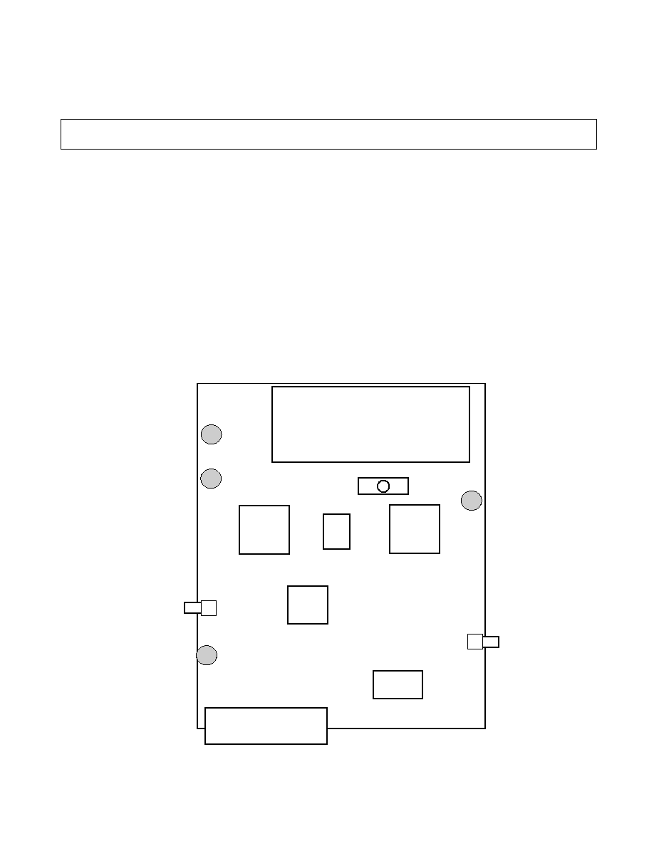
Figure 1. Evaluation Board Silkscreen
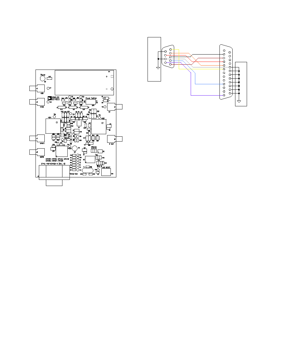
Figure 2. PC Cable Diagram
Hardware Description
The evaluation board comes with a cable for connecting to
the printer port of a PC. The silk screen and cable diagram for
the evaluation board are shown below. The board schematic is
shown on pages 3 and 4.
The board is powered from a single 9V battery. The power
supply ciruitry allows the user to choose either 3V or 5V for
the ADF4213 V
DD
and V
P
, and for the VCO supplies. The
default settings are 3V for the ADF4213 V
DD
and 5V for the
ADF4213 V
P
and for the VCO supplies. It is very important
to note that the ADF4213 V
DD
should never exceed the
ADF4213 V
P
. This can damage the device.
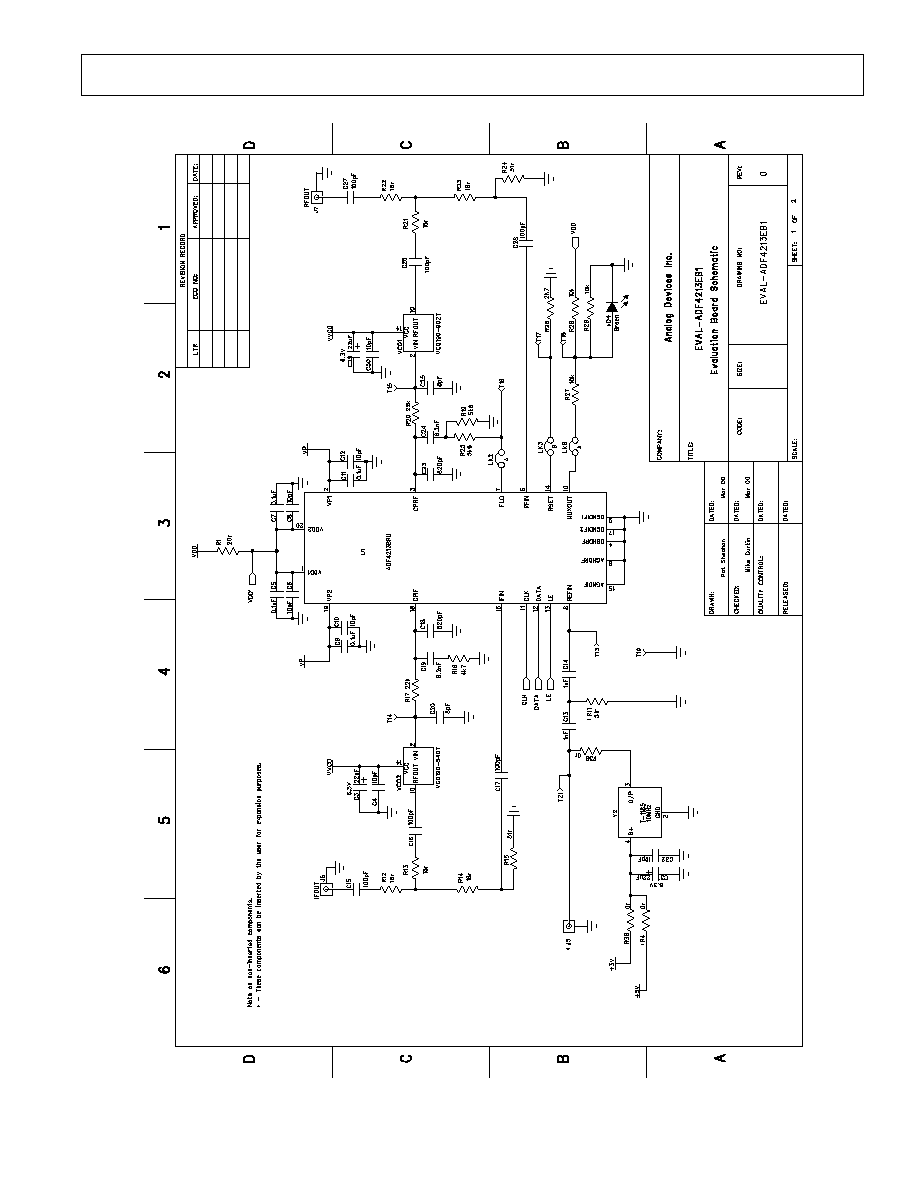
All components necessary for LO generation are on-board.
The 13MHz TCXO from Vectron provides the necessary
Reference Input. There are two channels controlled by the
ADF4213.
The RF PLL is made up of one half of the ADF4213, a pas-
sive loop filter (20kHz bandwidth) and the VCO 190-902T
from Vari-L. The output is available at RFOUT through a
standard SMA connector.
The IF PLL is made up of one half of the ADF4213, a pas-
sive loop filter (20kHz bandwidth) and the VCO 190-540T
from Vari-L. The output is available at IFOUT through a
standard SMA connector.
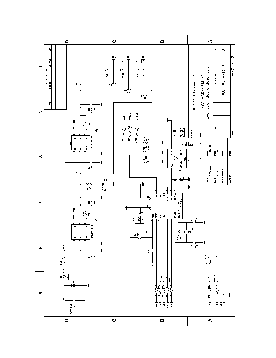
If the user wishes, they may use their own power supplies and
reference input. In this case, they need to insert SMA con-
nectors as shown on the silkscreen and block diagram.
The AD7706 A/D converter is used to monitor the power
supply voltage and current consumption of the ADF4213.
This helps the user pick the optimum synthesizer settings for
power consumption and also provides an alert if the battery
voltage is too low to sustain the required 3V or 5V for the
board supply.
RF loop component values shown in the circuit diagram are
for 900MHz RF output, 5mA CP current, VCO190-902T,
200kHz channel spacing and 20kHz loop bandwidth.
IF loop component values are for 540MHz IF output, 5mA
CP current, VCO190-540T, 200kHz channel spacing and
20kHz loop bandwidth.
1
2
3
7
8
9
11
12
14
15
16
17
18
19
20
21
22
23
24
25
1
2
3
4
5
6
7
8
9
Black - CLK
Brown - DATA
Red - LE
Orange - CE
ADF411X/ADF421X CABLE CONNECTIONS Rev 2 (15/3/99)
25 Way Male
D-Type
To
PC Printer Port
9 Way
Female D-Type
To
ADF411X
ADF421X
Evaluation
Board
PC
EVAL-ADF411X
EVAL-ADF421X
White - GND
6
4
5
Blue
Purple
Yellow
13
10
EVAL-ADF4213EB1
3
REV.PrA 12/00
Figure 3. Evaluation Board Circuit Diagram (Page 1)
EVAL-ADF4213EB1
REV.PrA 12/00
4
Figure 4. Evaluation Board Circuit Diagram (Page 2)
EVAL-ADF4213EB1
5
REV.PrA 12/00
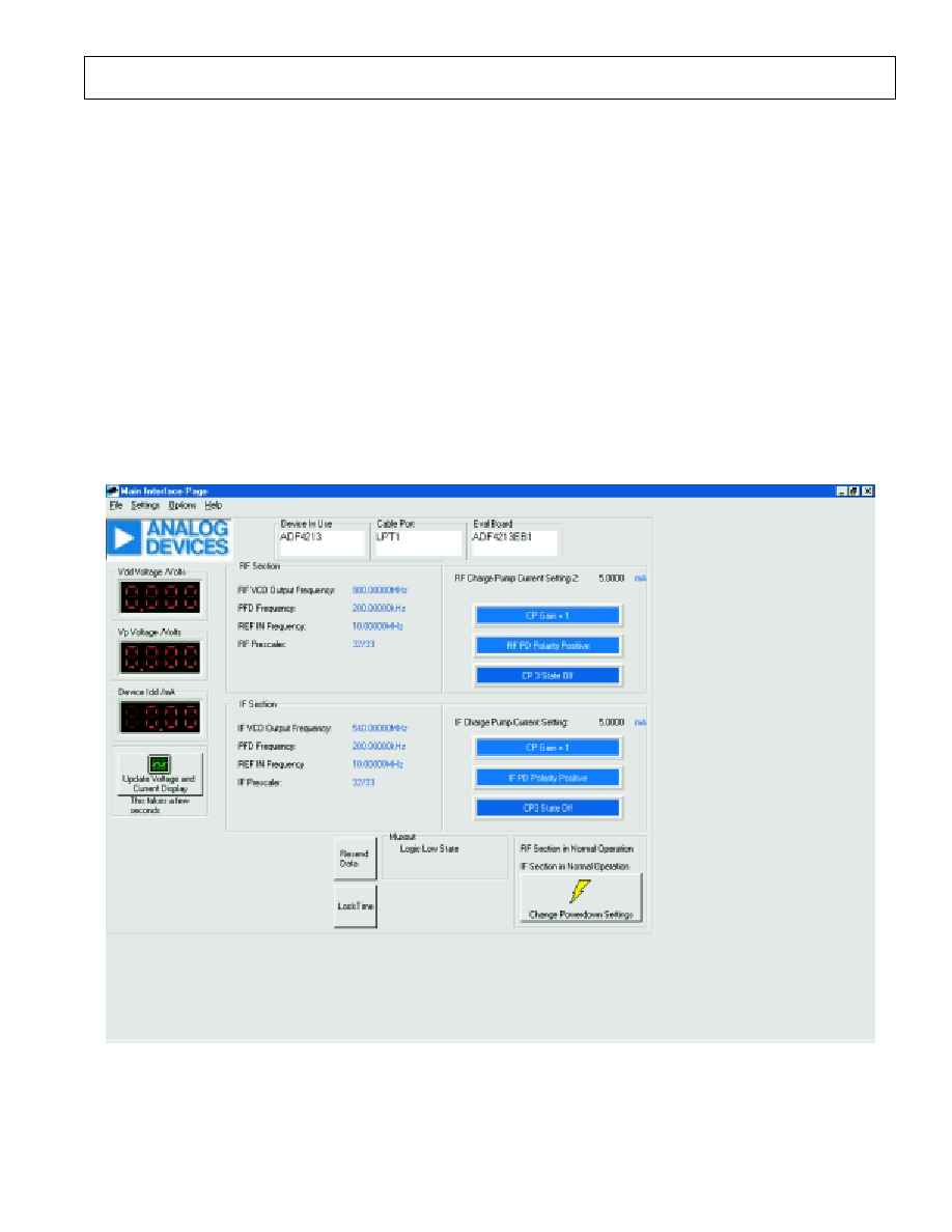
Figure 5. Software Front Panel
Software Description
The evaluation board software is contained on a CD-ROM
which comes in the package. To load the software the user
should click on "setup.exe" , then the install wizard installs
the software. Follow the on-screen directions. The software
will be installed in a default directory called "C:/Program
Files/Analog Devices". To run the software, simply go to the
Start Menu and choose Program/ADF4XXX/
ADF4XXX_rev2. This will open the software for the evalua-
tion board. The user will be asked to choose which device is
being evaluated. Click on the ADF4213 button. Hit OK. The
window shown below will now appear.
In this panel, click on the "Eval Board" button. Choose
ADF4213EB1 from the list on offer. Hit OK. The synthesizer
will now be programmed with the correct settings for a GSM
system working at 900MHz RF and 540MHz IF. 200kHz
PFD frequency is set up, 32/33 prescaler is chosen and charge
pump current of 5mA is programmed.
If the user wishes to change any of the settings then place the
cursor over the desired parameter (RF VCO Output Fre-
quency, for example) and click once. This brings up a screen
where it is possible to either type in a new value of output
frequency or else increment and decrement by the channel
spacing.
The software also allows monitoring of the device supply
voltage, supply current and the charge pump voltage. Simply
hit the "Update Voltage and Current Display" button to get
an up-to-date reading.
EVAL-ADF4213EB1
REV.PrA 12/00
6
Table 1. Bill of Materials for the EVAL-ADF4113EB1
Qty Reference
Description
Manufacturer
PCB DECAL
VALUE
1 U1
ADF4213BRU
ADI
TSSOP-20
ADF4213BRU
1 U2
AD7706BR
ADI
SO16WB
AD7706BR
1 U3
AD780A
ADI
SO8NB
AD780A
1 U4
ADP3300ART-5
ADI
SOT23-6
ADP3300ART-5
1 U5
ADP3300ART-3
ADI
SOT23-6
ADP3300ART-3
1 VCO1
902MHz VCO
Vari-L
VCO190-902T
1 VCO2
540MHz VCO
Vari-L
VCO190-540T
1 Y1
4.9152MHz Crystal
Vectron International
HC49 low profile
VXA4-1011
1 Y2
10 MHz TCXO
Vectron International
T-1185
1 D1
SD103C Schottky Diode
General Semiconductor
DO35
SD103
1 D2
IN4001
D03
FEC 365-117
1 D3
Red Low Power LE
Visha
LED
FEC 657-130
1 D4
Green Low Power LED (Do Not Insert)
Visha
LED
FEC 657-141
6 C1 C5 C7 C9 C11 C41
Multi Layer Ceramic Capacitor
Murata
Case 0603
0.1uF
1 C2
Tantalum CapacitorAVX
CAP\TAJ_B
10uF 6.3V
3 C3 C29 C31
Tantalum CapacitorAVX
CAP\TAJ_A
22uF 6.3V
7 C4 C6 C8 C10 C12 C30 C32
Multi Layer Ceramic Capacitor
Murata
Case 0603
10pF
2 C13-14
Multi Layer Ceramic Capacitor
Murata
Case 0603
1nF
6 C15-17 C26-28
Multi Layer Ceramic Capacitor
Murata
Case 0603
100pF
1 C18
Multi Layer Ceramic Capacitor
Murata
Case 0805
820pF
1 C19
Multi Layer Ceramic Capacitor
Murata
Case 0805
8.2nF
1 C20
Multi Layer Ceramic Capacitor
Murata
Case 0805
8pF
2 C21-22
Multi Layer Ceramic Capacitor
Murata
Case 0603
33pF
1 C23
Multi Layer Ceramic Capacitor
Murata
Case 0805
620pF
1 C24
Multi Layer Ceramic Capacitor
Murata
Case 0805
6.2nF
1 C25
Multi Layer Ceramic Capacitor
Murata
Case 0805
8pF
3 C33 C36 C40
Multi Layer Ceramic Capacitor
Murata
Case 0603
10nF
2 C34 C37
Tantalum CapacitorAVX
CAP\TAJ_A
1uF 16V
2 C35 C38
Tantalum CapacitorAVX
CAP\TAJ_A
4.7uF 10V
2 C39 C42
Tantalum CapacitorAVX
CAP\TAJ_A
10uF 6.3V
1 R1
Resistor (Surface Mount)
Bourns
Case 0805
20r 1.0%
7 R2 R5-10
Resistor (Surface Mount)
Bourns
Case 0603
330r 1.0%
1 R3
Resistor (Surface Mount)
Bourns
Case 0603
3k3 1.0%
1 R4
Do Not Insert
Bourns
Case 0603
1 R11
Do Not Insert
Bourns
Case 0603
6 R12-14 R21-23
Resistor (Surface Mount)
Bourns
Case 0603
18r 1.0%
2 R15 R24
Resistor (Surface Mount)
Bourns
Case 0603
51r 1.0%
1 R16
Resistor (Surface Mount)
Bourns
Case 0805
4k7 1.0%
1 R17
Resistor (Surface Mount)
Bourns
Case 0805
22k 1.0%
1 R18
Resistor (Surface Mount)
Bourns
Case 0603
1M 1.0%
1 R19
Resistor (Surface Mount)
Bourns
Case 0805
5k6 1.0%
1 R20
Resistor (Surface Mount)
Bourns
Case 0805
22k 1.0%
1 R25
Resistor (Surface Mount)
Bourns
Case 0805
5k6 1.0%
1 R26
Resistor (Surface Mount)
Bourns
Case 0603
2k7 1.0%
3 R27-29
Resistor (Surface Mount)
Bourns
Case 0603
10k 1.0%
6 R30-33 R40-41
Resistor (Surface Mount)
Meggitt
Case 0603
100k 0.1%
2 R34-35
Resistor (Surface Mount)
Bourns
Case 0603
0r 1.0%
2 R36 R37
Resistor (Surface Mount)
Bourns
Case 0603
330k 1.0%
2 R38 R39
Resistor (Surface Mount)
Bourns
Case 0603
0r 1.0%
1 R42
Resistor (Surface Mount)
Bourns
Case 0603
4k7 1.0%
1 SW1
Push Button Switch
Omron
SW\PB-SMALL
FEC 176-986
1 SW2
SPDT Switch - (Washable)
Apem
SW_SIP-3P
FEC 150-559
21 T1-21
Red Testpoint
W Hughes
TESTPOINT
FEC-240-345
1 J1
9 PIN D-TYPE MALE (HORIZ)
McMurdo
DCON9M
FEC 150-750
4 J2 J3 J4 J5 J6
Do Not Insert
SMA
2 J6 J7
GOLD 50
SMA SOCKET
Pasternack
SMA
PE4118
3 LK1 LK4 LK
3 pin headerHar
win
SIP-3P
FEC 512-047
3 LK2-A LK3-B LK6-A
Wire link
3 LK1 LK4 LK
Shorting Shunt
Harwin
FEC 150-410
4 Each Corner
Rubber Stick-On Feet
3M
FEC 148-922
2 P1
Pair PCB snap-on battery connector
Keystone
BATT_PP3
FEC 723-988
1 P1
9V PP3 Battery
Duracell
FEC 908-526
1 PCB
EVAL-ADF421XEB-5 (Rev. A)
Parts Free issued by ADI.