Äîêóìåíòàöèÿ è îïèñàíèÿ www.docs.chipfind.ru
a
EVAL-ADF421XEB1
FEATURES
General Purpose PLL Evaluation Board excluding Synthe-
sizer, VCOs, Loop Filters for generating generic PLL
standards.
Compatible with ADF4210 and ADF4216 synthesizer fami-
lies.
Accompanying Software allows complete control of syn-
thesizer functions from PC
Battery Operated: Choice of 3V or 5V supplies
© Analog Devices, Inc., 1999
One Technology Way, P.O. Box 9106, Norwood, MA 02062-9106, U.S.A.
Tel: 781-329-4700
Fax: 781-326-8703
Information furnished by Analog Devices is believed to be accurate and reliable. However,
no responsibility is assumed by Analog Devices for its use, nor for any infringements of
patents or other rights of third parties which may result from its use. No license is granted
by implication or otherwise under any patent or patent rights of Analog Devices.
Evaluation Board For PLL Frequency
Synthesizer
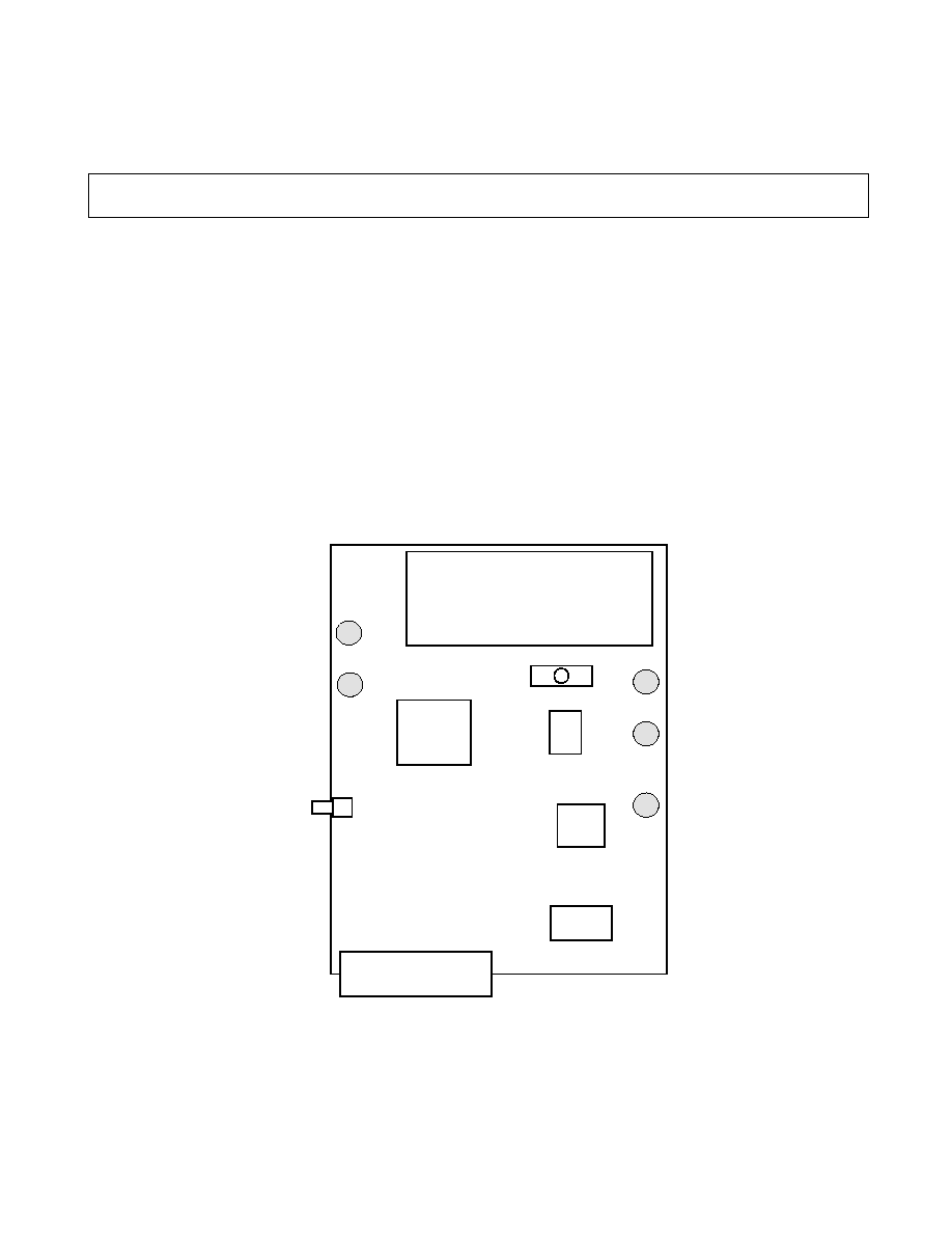
BLOCK DIAGRAM
REV.PrA 02/00
GENERAL DESCRIPTION
This board is designed to allow the user to evaluate
the performance of the ADF421X Frequency Synthe-
sizer for PLL's (Phase Locked Loops). The block
diagram of the board is shown below. It contains the
footprint for a ADF421X synthesizer, a pc connector,
SMA connector for the reference input, power sup-
plies and RF output. There is also a footprint for a
loop filter and a VCO for both the RF and IF section
on board. A cable is included with the board to con-
nect to a pc printer port.
The package also contains windows software to allow
easy programming of the synthesizer.
V C O 1
(V ari-L )
P C C O N NE C T O R
9V B A T T ER Y
A D F 4 11X
E VA L -A D F 41 1X E B 1
V
P
C E
R EF
IN
R F
O U T
V
V C O
V
D D
V C O 1 90-X X XT
T C X O
V ectr o n
A D 7 706
S M A
S oc ke t
P O W E R S W IT C H
O N
O F F
EVAL-ADF421XEB1
REV.PrA 02/00
2
Figure 1. Evaluation Board Silkscreen
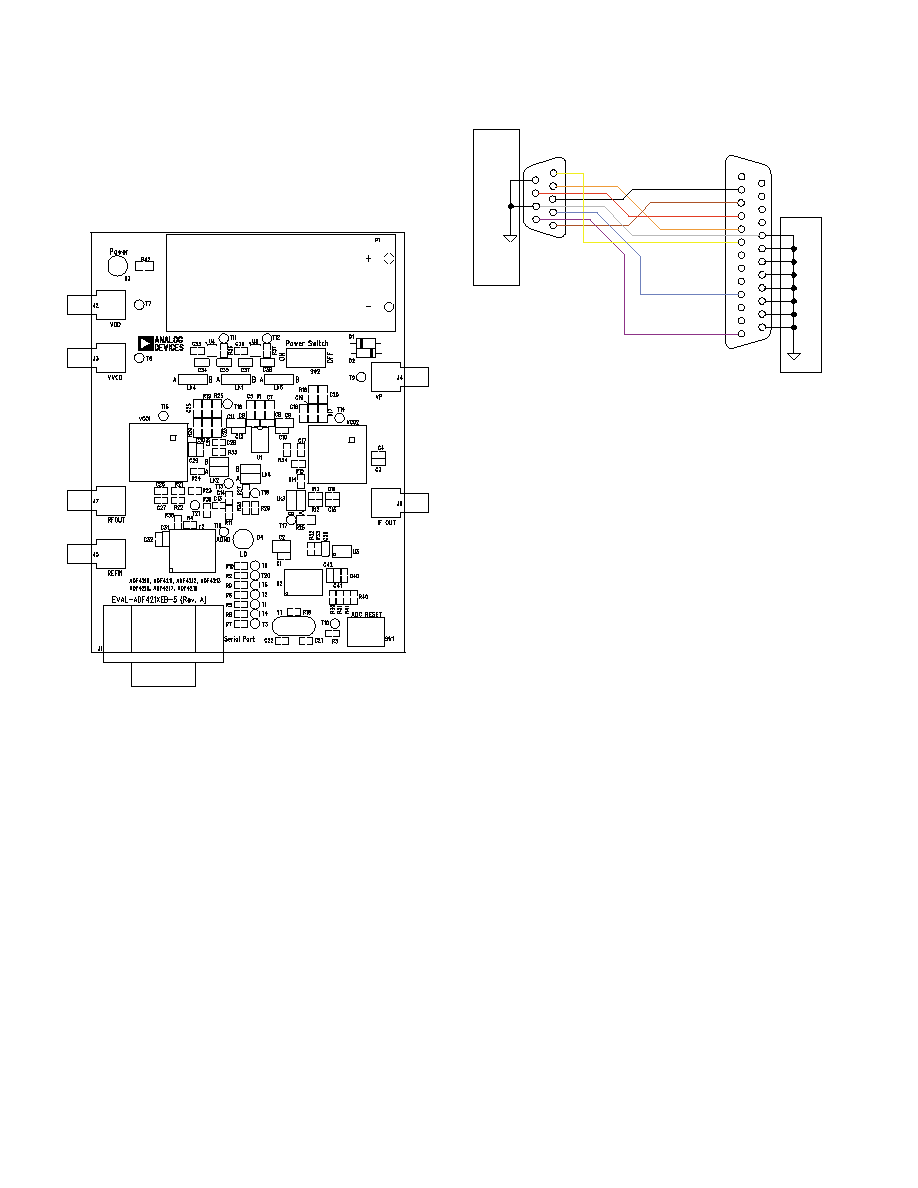
Figure 2. PC Cable Diagram
1
2
3
7
8
9
11
12
14
15
16
17
18
19
20
21
22
23
24
25
1
2
3
4
5
6
7
8
9
Black - CLK
Brown - DATA
Red - LE
Orange - CE
25 Way Male
D-Type
To
PC Printer Port
9 Way
Female D-Type
To
ADF411X
ADF421X
Evaluation
Board
PC
EVAL-ADF411X
EVAL-ADF421X
White - GND
6
4
5
Blue
Purple
Yellow
13
10
Hardware Description
The evaluation board comes with a cable for connecting to
the printer port of a PC. The silk screen and cable diagram for
the evaluation board are shown below. The board schematic is
shown on pages 3 and 4.
The board is powered from a single 9V battery. The
power supply ciruitry allows the user to choose either 3V
or 5V for the ADF4113 V
DD
and V
P
, and for the VCO
supply. The default settings are 3V for the ADF411X V
DD
and 5V for the ADF411X V
P
and for the VCO supply. It
is very important to note that the ADF4113 V
DD
should
never exceed the ADF411X V
P
. This can damage the de-
vice.
All components necessary for LO generation are catered
for on-board. The TCXO connector provides the neces-
sary Reference Input. The PLL is made up of the
ADF411X, passive loop filter and the VCO 190-XXXT
from Vari-L. The output is available at RFOUT through
a standard SMA connector. If the user wishes they may
use their own power supplies and reference input. In this
case, they need to insert SMA connectors to as shown on
the silkscreen and block diagram.
The AD7706 A/D converter is used to monitor the power
supply voltage and current consumption of the ADF411X.
This helps the user pick the optimum synthesizer settings for
power consumption and also provides an alert if the battery
voltage is too low to sustain the required 3V or 5V for the
board supply.
Loop component values shown in the circuit diagram are
for 900MHz RF output, 5mA CP current, VCO190-
902T, 200kHz channel spacing and 20kHz loop band-
width.
EVAL-ADF421XEB1
3
REV.PrA 02/00
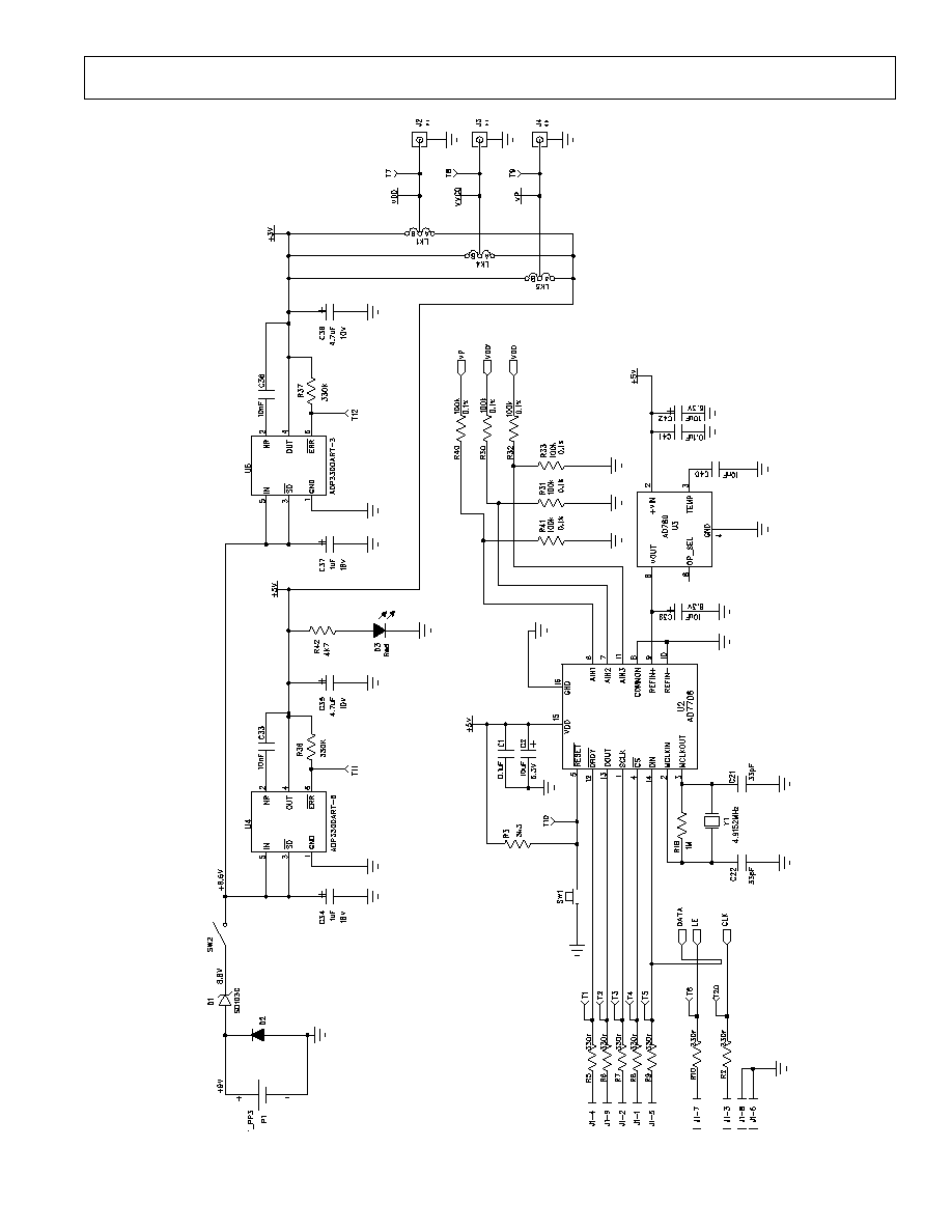
Figure 3. Evaluation Board Circuit Diagram (Page 1)
EVAL-ADF421XEB1
REV.PrA 02/00
4
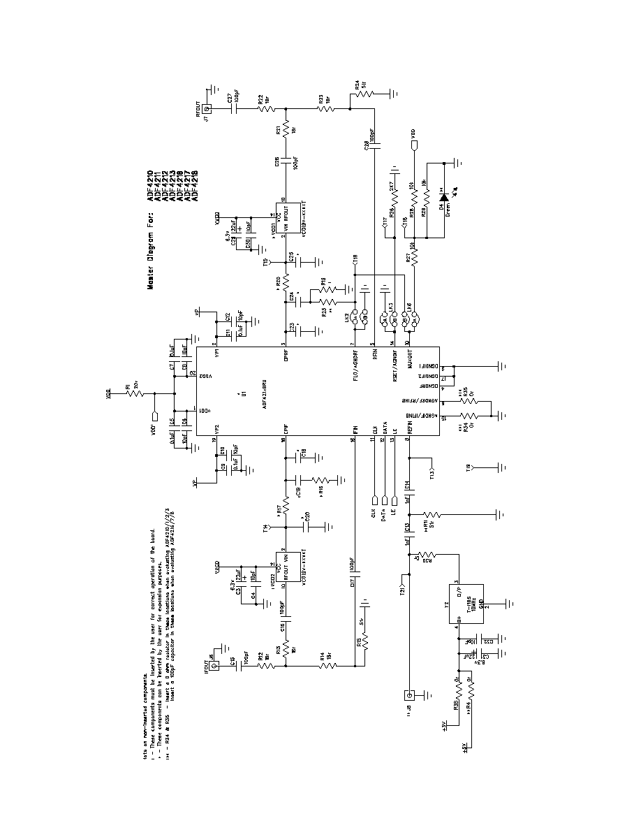
Figure 4. Evaluation Board Circuit Diagram (Page 2)
EVAL-ADF421XEB1
5
REV.PrA 02/00
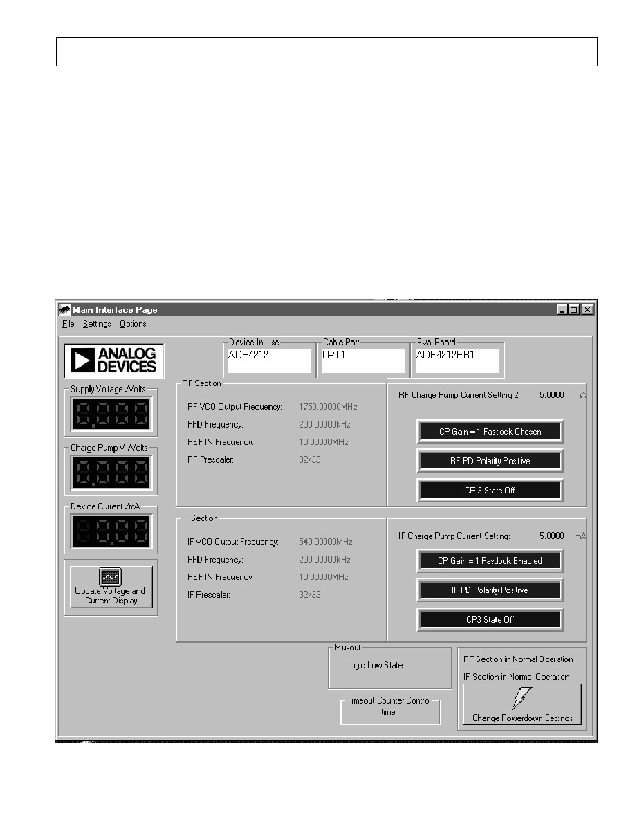
Figure 5. Software Front Panel
Software Description
The software comes on a set of two floppy disks (Disk 1 and
Disk 2). If the user double clicks on "setup.exe" on Disk 1,
then the install wizard installs the software. Follow the on-
screen directions. The software will be installed in a default
directory called "C:/Program Files/Project1". To run the
software, simply double-click on "adf411X.exe".
The front panel of the evaluation board software is shown
below.
When the main software screen appears, follow the steps
below for initial setup to interface to the part.
Click on Choose Device, and the Device window will appear.
Choose the device being evaluated and click OK.
Click on Choose Port, and the Port Connector window will
appear. Choose the port that the cable is connected to on the
PC and click OK. (Normally LPT1)
Click on Osc In, and the Crystal Frequency window will
appear. Enter the reference frequency being used and click
OK.
Click on RF VCO Output Frequency, and the Output
Frequency window will appear. Enter the output frequency
and PFD reference frequency, and click OK.
Click On Prescaler, and the Prescaler window will appear.
Grab the pointer, and choose the desired prescaler value.
Click OK.
Click on the RF PD Polarity button to set the RF PD Polarity
bit High.
Click on Charge Pump Current Setting 2 or Charge Pump
Current Setting 1 and the Current Setting window will ap-
pear. Grab the pointer to set the Charge Pump Current Set-
ting. Click OK.
The data is now set up, and other features can now be exam-
ined by the user.