Äîêóìåíòàöèÿ è îïèñàíèÿ www.docs.chipfind.ru
Multichannel ISM Band
FSK/GFSK/OOK/GOOK/ASK Transmitter
ADF7012
Rev. 0
Information furnished by Analog Devices is believed to be accurate and reliable.
However, no responsibility is assumed by Analog Devices for its use, nor for any
infringements of patents or other rights of third parties that may result from its use.
Specifications subject to change without notice. No license is granted by implication
or otherwise under any patent or patent rights of Analog Devices. Trademarks and
registered trademarks are the property of their respective owners.
One Technology Way, P.O. Box 9106, Norwood, MA 02062-9106, U.S.A.
Tel: 781.329.4700
www.analog.com
Fax: 781.326.8703
© 2004 Analog Devices, Inc. All rights reserved.
FEATURES
Single-chip, low power UHF transmitter
75 MHz to 1 GHz frequency operation
Multichannel operation using Frac-N PLL
2.3 V to 3.6 V operation
On-board regulator--stable performance
Programmable output power:
-16 dBm to +14 dBm, 0.4 dB steps
Data rates: dc to 179.2 kbps
Low current consumption:
868 MHz, 10 dBm, 21 mA
433 MHz, 10 dBm, 17 mA
315 MHz, 0 dBm, 10 mA
Programmable low battery voltage indicator
24-lead TSSOP
APPLICATIONS
Low cost wireless data transfer
Security systems
RF remote controls
Wireless metering
Secure keyless entry
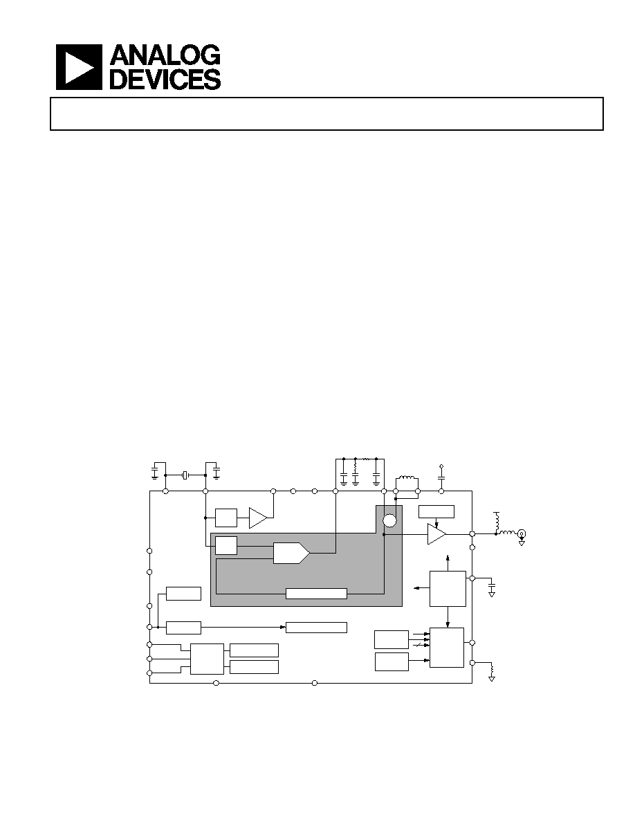
GENERAL DESCRIPTION
The ADF7012 is a low power FSK/GFSK/OOK/GOOK/ASK
UHF transmitter designed for short range devices (SRDs). The
output power, output channels, deviation frequency, and mod-
ulation type are programmable by using four, 32-bit registers.
The fractional-N PLL and VCO with external inductor enable
the user to select any frequency in the 75 MHz to 1 GHz band.
The fast lock times of the fractional-N PLL make the ADF7012
suitable in fast frequency hopping systems. The fine frequency
deviations available and PLL phase noise performance facilitates
narrow-band operation.
There are five selectable modulation schemes: binary frequency
shift keying (FSK), Gaussian frequency shift keying (GFSK),
binary on-off keying (OOK), Gaussian on-off keying (GOOK),
and amplitude shift keying (ASK). In the compensation register,
the output can be moved in <1 ppm steps so that indirect com-
pensation for frequency error in the crystal reference can be
made.
A simple 3-wire interface controls the registers. In power-down,
the part has a typical quiescent current of <0.1 A.
FUNCTIONAL BLOCK DIAGRAM
SERIAL
INTERFACE
FREQUENCY
COMPENSATION
CENTER
FREQUENCY
OSC1
OSC2
L1
L2
C
VCO
CLK
OUT
CPV
DD
CP
GND
C
REG
PRINTED
INDUCTOR
A
GND
CE
LE
DATA
CLK
TxDATA
TxCLK
MUXOUT
RF GND
R
SET
RF
OUT
C
REG
V
DD
D
GND
DV
DD
FSK\GFSK
OOK\ASK
OOK\ASK
÷
CLK
÷
R
PFD/
CHARGE
PUMP
-
+FRACTIONAL N
VCO
PLL LOCK
DETECT
MUXOUT
LDO
REGULATOR
BATTERY
MONITOR
PA
04617-0-001
Figure 1.

ADF7012
Rev. 0 | Page 2 of 28
TABLE OF CONTENTS
Specifications..................................................................................... 3
Timing Characteristics..................................................................... 5
Absolute Maximum Ratings............................................................ 6
Transistor Count........................................................................... 6
ESD Caution.................................................................................. 6
Pin Configuration and Function Descriptions............................. 7
Typical Performance Characteristics ............................................. 8
315 MHz ........................................................................................ 8
433 MHz ........................................................................................ 9
868 MHz ...................................................................................... 10
915 MHz ...................................................................................... 11
Circuit Description......................................................................... 12
PLL Operation ............................................................................ 12
Crystal Oscillator........................................................................ 12
Crystal Compensation Register................................................ 12
Clock Out Circuit ....................................................................... 12
Loop Filter ................................................................................... 13
Voltage-Controlled Oscillator (VCO) ..................................... 13
Voltage Regulators...................................................................... 13
FSK Modulation.......................................................................... 13
GFSK Modulation ...................................................................... 14
Power Amplifier.......................................................................... 14
GOOK Modulation .................................................................... 15
Output Divider ........................................................................... 16
MUXOUT Modes....................................................................... 16
Theory of Operation ...................................................................... 17
Choosing the External Inductor Value.................................... 17
Choosing the Crystal/PFD Value............................................. 17
Tips on Designing the Loop Filter ........................................... 17
PA Matching................................................................................ 18
Transmit Protocol and Coding Considerations ..................... 18
Application Examples .................................................................... 19
315 MHz Operation ................................................................... 20
433 MHz Operation ................................................................... 21
868 MHz Operation ................................................................... 22
915 MHz Operation ................................................................... 23
Register Descriptions ..................................................................... 24
R Register..................................................................................... 24
N-Counter Latch ........................................................................ 25
Modulation Register .................................................................. 26
Function Register ....................................................................... 27
Outline Dimensions ....................................................................... 28
Ordering Guide .......................................................................... 28
REVISION HISTORY
10/04--Revision 0: Initial Version
ADF7012
Rev. 0 | Page 3 of 28
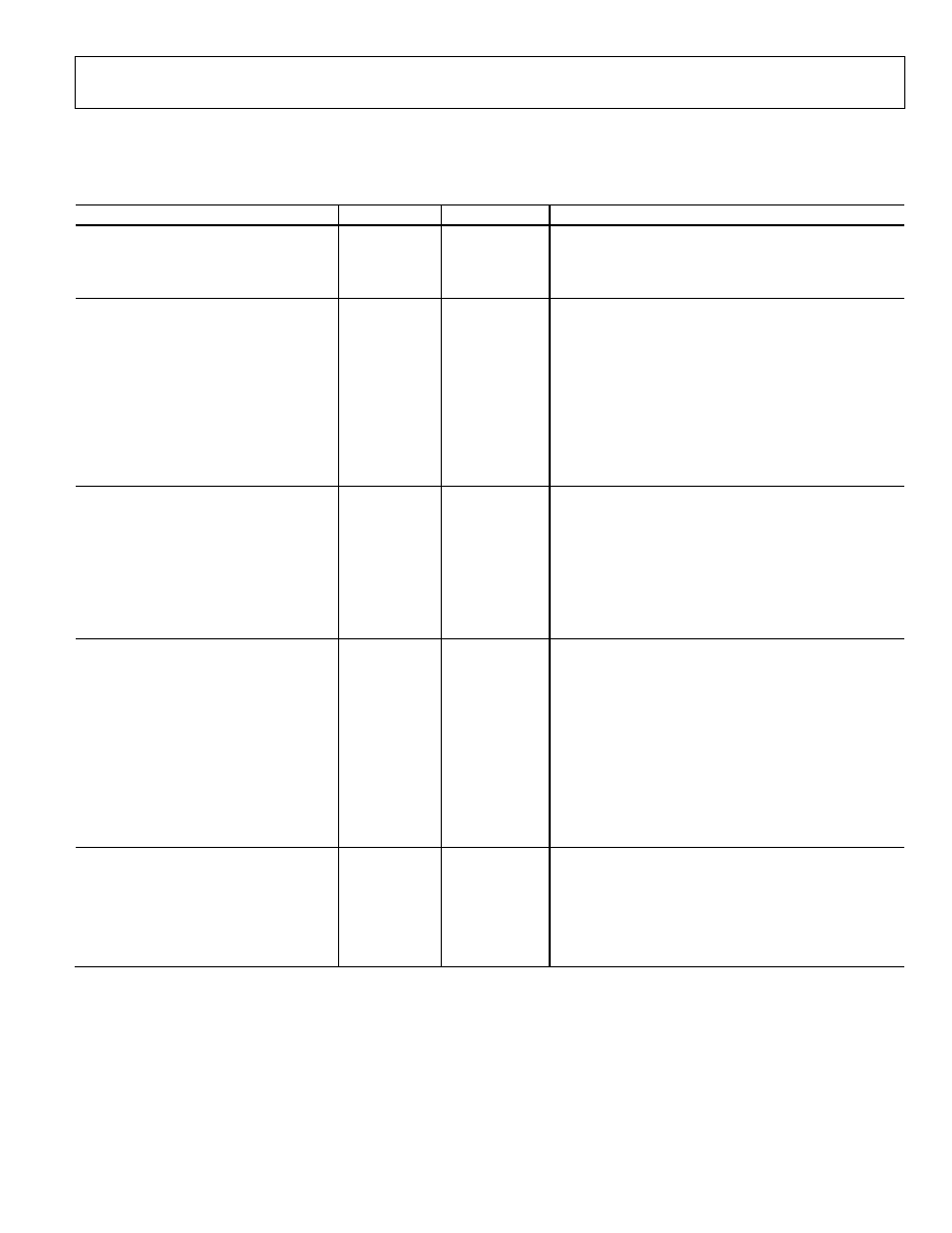
SPECIFICATIONS
DV
DD
= 2.3 V 3.6 V; AGND = DGND = 0 V; T
A
= T
MIN
to T
MAX
, unless otherwise noted. Operating temperature range is -40°C to +85°C.
Table 1.
Parameter B
Version
Unit
Conditions/Comments
RF OUTPUT CHARACTERISTICS
Operating Frequency
75/1000
MHz min/max
VCO range adjustable using external inductor;
divide-by-2, -4, -8 options may be required
Phase Frequency Detector
F
RF
/128 Hz
min
MODULATION PARAMETERS
Data Rate FSK/GFSK
179.2
kbps
Using 1 MHz loop bandwidth
Data Rate ASK/OOK
64
Kbps
Based on US FCC 15.247 specfications for ACP; higher
data rates are achievable depending on local regulations
Deviation FSK/GFSK
PFD/2
14
Hz min
For example, 10 MHz PFD deviation min = ± 610 Hz
511 × PFD/2
14
Hz max
For example, 10 MHz PFD deviation max = ± 311.7 kHz
GFSK BT
0.5
typ
ASK Modulation Depth
25
dB max
OOK Feedthrough (PA Off)
-40
dBm typ
F
RF
= Fvco
-80
dBm
typ
F
RF
= Fvco/2
POWER AMPLIFIER PARAMETERS
Max Power Setting, DV
DD
= 3.6 V
14
dBm
F
RF
= 915 MHz, PA is matched into 50
Max Power Setting, DV
DD
= 3.0 V
13.5
dBm
F
RF
= 915 MHz, PA is matched into 50
Max Power Setting, DV
DD
= 2.3 V
12.5
dBm
F
RF
= 915 MHz, PA is matched into 50
Max Power Setting, DV
DD
= 3.6 V
14.5
dBm
F
RF
= 433 MHz, PA is matched into 50
Max Power Setting, DV
DD
= 3.0 V
14
dBm
F
RF
= 433 MHz, PA is matched into 50
Max Power Setting, DV
DD
= 2.3 V
13
dBm
F
RF
= 433 MHz, PA is matched into 50
PA Programmability
0.4
dB typ
PA output = -20 dBm to +13 dBm
POWER SUPPLIES
DV
DD
2.3/3.6
V min/V max
Current Comsumption
315 MHz, 0 dBm/5 dBm
8/14
mA typ
DV
DD
= 3.0 V, PA is matched into 50 , IVCO = min
433 MHz, 0 dBm/10 dBm
10/18
mA typ
868 MHz, 0 dBm/10 dBm/14 dBm 14/21/32 mA
typ
915 MHz, 0 dBm/10 dBm/14 dBm
16/24/35
mA typ
VCO Current Consumption
1/8
mA min/max
VCO current consumption is programmable
Crystal Oscillator Current Consumption
190
µA typ
Regulator Current Consumption
280
µA typ
Power-Down Current
0.1/1
µA typ/max
REFERENCE INPUT
Crystal Reference Frequency
3.4/26
MHz min/max
Single-Ended Reference Frequency 3.4/26
MHz
min/max
Crystal Power-On Time 3.4 MHz/26 MHz
1.8/2.2
ms typ
CE to Clock Enable Valid
Single-Ended Input Level
CMOS Levels
Refer to the LOGIC INPUTS parameter. Applied to OSC 2
oscillator circuit disabled.
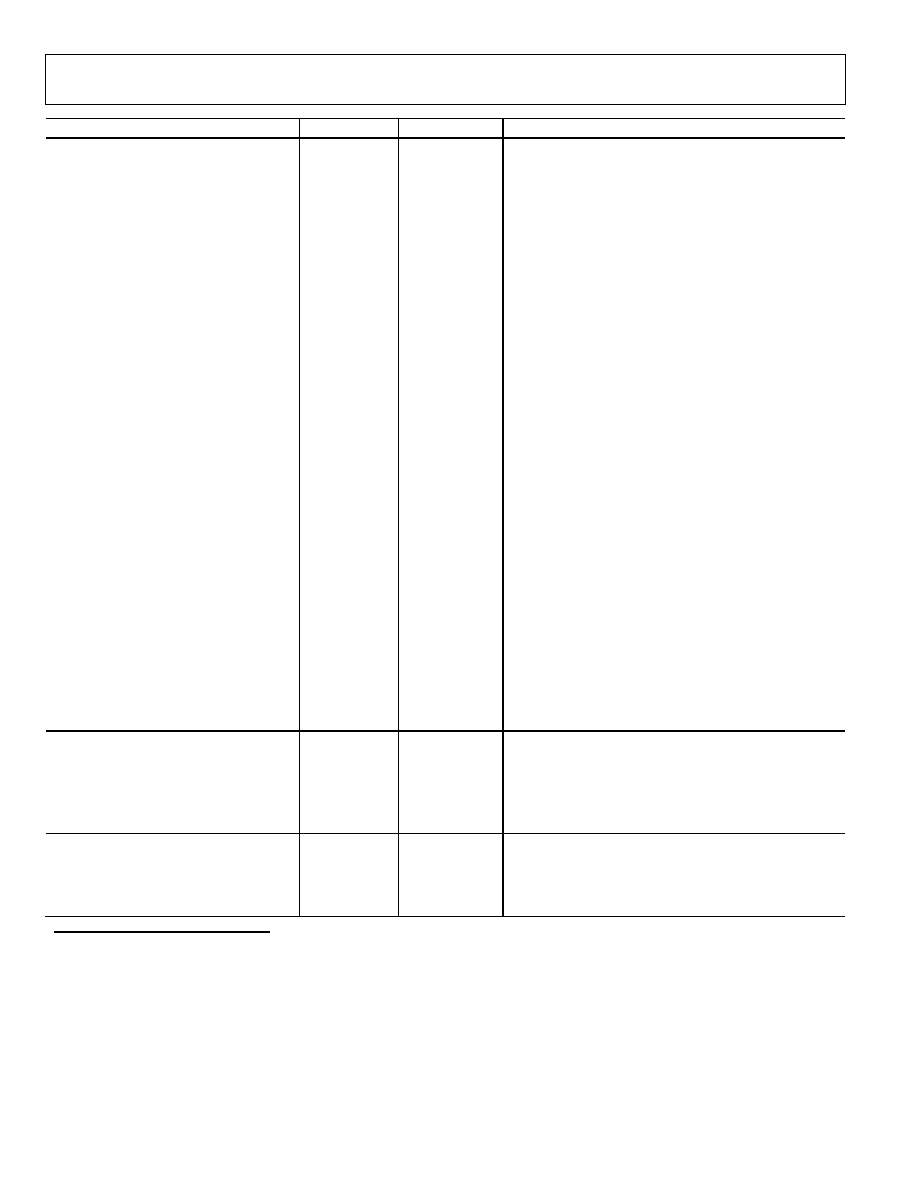
ADF7012
Rev. 0 | Page 4 of 28
Parameter B
Version
Unit
Conditions/Comments
PHASE-LOCKED LOOP PARAMETERS
VCO Gain
315MHz
22
MHz/V typ
VCO divide-by-2 active
433MHz
24
MHz/V typ
VCO divide-by-2 active
868MHz 80
MHz/V
typ
915MHz 88
MHz/V
typ
VCO Tuning Range
0.3/2.0
V min/max
Spurious (IVCO Min/Max) -65/-70
dBc
I
VCO
is programmable
Charge Pump Current
Setting [00]
0.3
mA typ
Refering to DB[7:6] in Function Register
Setting [01]
0.9
mA typ
Refering to DB[7:6] in Function Register
Setting [10]
1.5
mA typ
Refering to DB[7:6] in Function Register
Setting [11]
2.1
mA typ
Refering to DB[7:6] in Function Register
Phase Noise (In band)
1
315MHz
-85
dBc/Hz typ
PFD = 10 MHz, 5 kHz offset, I
VCO
= 2 mA
433MHz
-83
dBc/Hz typ
PFD = 10 MHz, 5 kHz offset, I
VCO
= 2 mA
868MHz
-80
dBc/Hz typ
PFD = 10 MHz, 5 kHz offset, I
VCO
= 3 mA
915MHz
-80
dBc/Hz typ
PFD = 10 MHz, 5 kHz offset, I
VCO
= 3 mA
Phase Noise (Out of Band)
1
315MHz
-103
dBc/Hz typ
PFD = 10 MHz, 1 MHz offset, I
VCO
= 2 mA
433MHz
-104
dBc/Hz typ
PFD = 10 MHz, 1 MHz offset, I
VCO
= 2 mA
868MHz
-115
dBc/Hz typ
PFD = 10 MHz, 1 MHz offset, I
VCO
= 3 mA
915MHz
-114
dBc/Hz typ
PFD = 10 MHz, 1 MHz offset, I
VCO
= 3 mA
Harmonic Content (Second)
2
-20 dBc
typ
F
RF
= F
VCO
Harmonic Content (Third)
2
-30
dBc typ
Harmonic Content (Others)
2
-27
dBc
typ
Harmonic Content (Second)
2
-24 dBc
typ
F
RF
= F
VCO
/N (where N = 2, 4, 8)
Harmonic Content (Third)
2
-14
dBc typ
Harmonic Content (Others)
2
-19
dBc
typ
LOGIC INPUTS
Input High Voltage,V
INH
0.7 × DV
DD
V min
Input Low Voltage, V
INL
0.2 × DV
DD
V max
Input Current, I
INH
/I
INL
±1
µA max
Input Capacitance, C
IN
4.0
pF max
LOGIC OUTPUTS
Output High Voltage, V
OH
DV
DD
- 0.4
V min
CMOS output chosen
Output High Current, I
OH
,
500
µA max
Output Low Voltage, V
OL
0.4
V max
I
OL
= 500 µA
1
Measurements made with N
FRAC
= 2048.
2
Measurements made without harmonic filter.
ADF7012
Rev. 0 | Page 5 of 28
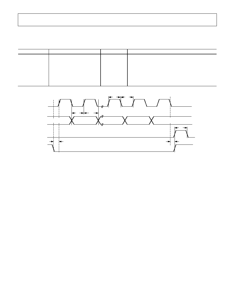
TIMING CHARACTERISTICS
DV
DD
= 3 V ± 10%; AGND = DGND = 0 V; T
A
= T
MIN
to T
MAX
, unless otherwise noted.
Table 2.
Parameter
Limit at T
MIN
to T
MAX
(B Version)
Unit
Test Conditions/Comments
t
1
20
ns min
LE setup time
t
2
10
ns min
Data-to-clock setup time
t
3
10
ns min
Data-to-clock hold time
t
4
25
ns min
Clock high duration
t
5
25
ns min
Clock low duration
t
6
10
ns min
Clock to-LE setup time
t
7
20
ns min
LE pulse width
CLOCK
DATA
LE
LE
DB23 (MSB)
DB22
DB2
DB1
(CONTROL BIT C2)
DB0 (LSB)
(CONTROL BIT C1)
t
1
t
2
t
3
t
7
t
6
t
4
t
5
04617-0-002
Figure 2. Timing Diagram
Document Outline