Äîêóìåíòàöèÿ è îïèñàíèÿ www.docs.chipfind.ru
High Performance
ISM Band Transceiver IC
ADF7025
Rev. A
Information furnished by Analog Devices is believed to be accurate and reliable. However, no
responsibility is assumed by Analog Devices for its use, nor for any infringements of patents or other
rights of third parties that may result from its use. Specifications subject to change without notice. No
license is granted by implication or otherwise under any patent or patent rights of Analog Devices.
Trademarks and registered trademarks are the property of their respective owners.
One Technology Way, P.O. Box 9106, Norwood, MA 02062-9106, U.S.A.
Tel: 781.329.4700
www.analog.com
Fax: 781.461.3113
©2006 Analog Devices, Inc. All rights reserved.
FEATURES
Low power, zero-IF RF transceiver
Frequency bands
431 MHz to 464 MHz
862 MHz to 870 MHz
902 MHz to 928 MHz
Data rates supported
9.6 kbps to 384 kbps, FSK
2.3 V to 3.6 V power supply
Programmable output power
-16 dBm to +13 dBm in 63 steps
Receiver sensitivity
-104.2 dBm at 38.4 kbps, FSK
-100 dBm at 172.8 kbps, FSK
-95.8 dBm at 384 kbps, FSK
Low power consumption
19 mA in receive mode
28 mA in transmit mode (10 dBm output)
On-chip VCO and Fractional-N PLL
On-chip, 7-bit ADC and temperature sensor
Digital RSSI
Integrated TRx switch
Leakage current < 1 µA in power-down mode
APPLICATIONS
Wireless audio/video
Remote control/security systems
Wireless metering
Keyless entry
Home automation
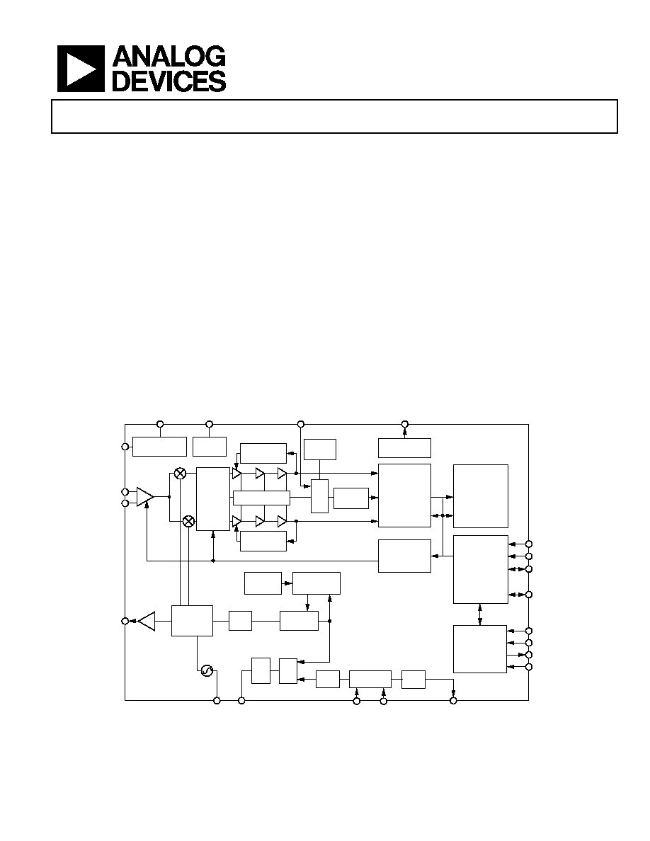
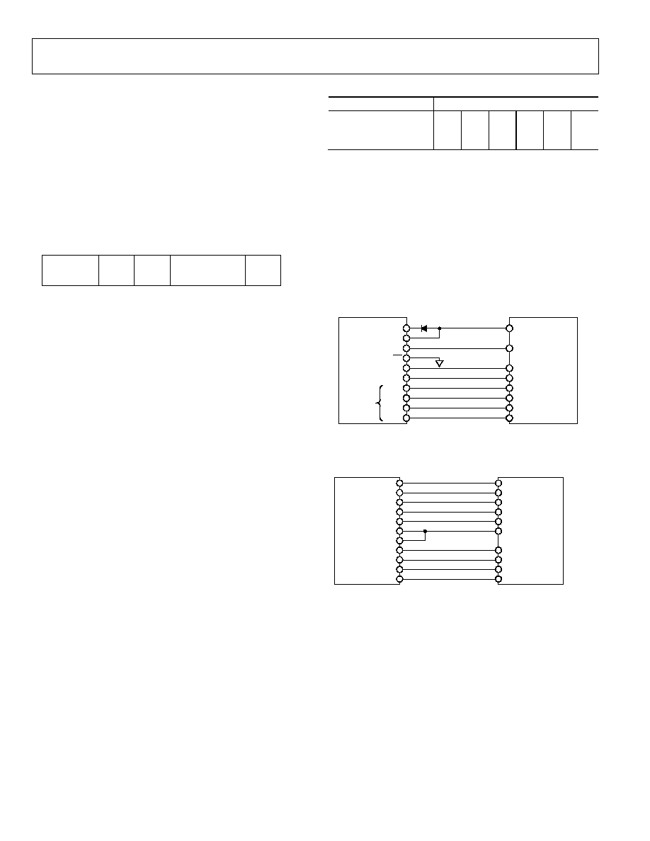
FUNCTIONAL BLOCK DIAGRAM
Tx/Rx
CONTROL
AGC
CONTROL
FSK
DEMODULATOR
DATA
SYNCHRONIZER
RSSI
7-BIT ADC
GAIN
DIV R
SERIAL
PORT
RFOUT
OFFSET
CORRECTION
OFFSET
CORRECTION
LNA
VCO
PFD
CP
OSC1
OSC2
DIVIDERS/
MUXING
N/N+1
DIV P
MUX
TEMP
SENSOR
RING
OSC
CLK
DIV
CLKOUT
TEST MUX
VCOIN CPOUT
BIAS
LDO(1:4)
MUXOUT
ADCIN
RSET
CREG(1:4)
R
LNA
R
FIN
R
FINB
SLE
SDATA
CE
DATA CLK
SREAD
SCLK
INT/LOCK
DATA I/O
FSK MOD
CONTROL
-
MODULATOR
LP FILTER
05
54
2-
00
1
Figure 1.

ADF7025
Rev. A | Page 2 of 44
TABLE OF CONTENTS
Features .............................................................................................. 1
Applications....................................................................................... 1
Functional Block Diagram .............................................................. 1
Revision History ............................................................................... 2
General Description ......................................................................... 3
Specifications..................................................................................... 4
Timing Characteristics..................................................................... 7
Timing Diagrams.......................................................................... 7
Absolute Maximum Ratings............................................................ 9
ESD Caution.................................................................................. 9
Pin Configuration and Function Descriptions........................... 10
Typical Performance Characteristics ........................................... 12
Frequency Synthesizer ................................................................... 15
Reference Input Section............................................................. 15
Choosing Channels for Best System Performance................. 17
Transmitter ...................................................................................... 18
RF Output Stage.......................................................................... 18
Modulation Scheme ................................................................... 18
Receiver............................................................................................ 19
RF Front End............................................................................... 19
RSSI/AGC.................................................................................... 20
FSK Demodulators on the ADF7025....................................... 20
FSK Correlator/Demodulator................................................... 20
Linear FSK Demodulator .......................................................... 22
Automatic Sync Word Recognition ......................................... 22
Applications Section....................................................................... 23
LNA/PA Matching...................................................................... 23
Transmit Protocol and Coding Considerations ..................... 24
Device Programming after Initial Power-Up ............................. 24
Interfacing to Microcontroller/DSP ........................................ 24
Serial Interface ................................................................................ 27
Readback Format........................................................................ 27
Registers........................................................................................... 28
Register 0--N Register............................................................... 28
Register 1--Oscillator/Filter Register...................................... 29
Register 2--Transmit Modulation Register ............................ 30
Register 3--Receiver Clock Register ....................................... 31
Register 4--Demodulator Setup Register ............................... 32
Register 5--Sync Byte Register................................................. 33
Register 6--Correlator/Demodulator Register ...................... 34
Register 7--Readback Setup Register...................................... 35
Register 8--Power-Down Test Register .................................. 36
Register 9--AGC Register......................................................... 37
Register 10--AGC 2 Register.................................................... 38
Register 12--Test Register......................................................... 39
Register 13--Offset Removal and Signal Gain Register ....... 40
Outline Dimensions ....................................................................... 41
Ordering Guide .......................................................................... 41
REVISION HISTORY
2/06--Rev. 0 to Rev. A
Replaced Figure 40 ................................................................ Page 29
1/06--Revision 0: Initial Version

ADF7025
Rev. A | Page 3 of 44
GENERAL DESCRIPTION
The ADF7025 is a low power, highly integrated FSK transceiver.
It is designed for operation in the licensefree ISM bands of
433 MHz, 863 MHz to 870 MHz, and 902 MHz to 928 MHz.
The ADF7025 can be used for applications operating under the
European ETSI EN300-220 or the North American FCC (Part 15)
regulatory standards. The ADF7025 is intended for wideband,
high data rate applications with deviation frequencies from
100 kHz to 750 kHz and data rates from 9.6 kbps to 384 kbps.
A complete transceiver can be built using a small number of
external discrete components, making the ADF7025 very
suitable for price-sensitive and area-sensitive applications.
The transmit section contains a VCO and low noise
Fractional-N PLL with output resolution of <1 ppm. The VCO
operates at twice the fundamental frequency to reduce spurious
emissions and frequency pulling problems.
The transmitter output power is programmable in 0.3 dB steps
from -16 dBm to +13 dBm. The transceiver RF frequency, channel
spacing, and modulation are programmable using a simple 3-wire
interface. The device operates with a power supply range of 2.3 V
to 3.6 V and can be powered down when not in use.
A zero-IF architecture is used in the receiver, minimizing power
consumption and the external component count, while avoiding
the need for image rejection. The baseband filter (low-pass) has
programmable bandwidths of ±300 kHz, ±450 kHz, and ±600 kHz.
A high-pass pole at ~60 kHz eliminates the problem of dc offsets
that is characteristic of zero-IF architecture.
The ADF7025 supports a wide variety of programmable
features, including Rx linearity, sensitivity, and filter bandwidth,
allowing the user to trade off receiver sensitivity and selectivity
against current consumption, depending on the application.
An on-chip ADC provides readback of an integrated tempera-
ture sensor, an external analog input, the battery voltage, or the
RSSI signal, which provides savings on an ADC in some
applications. The temperature sensor is accurate to ±10°C over
the full operating temperature range of -40°C to +85°C. This
accuracy can be improved by doing a 1-point calibration at
room temperature and storing the result in memory.

ADF7025
Rev. A | Page 4 of 44
SPECIFICATIONS
V
DD
= 2.3 V to 3.6 V, GND = 0 V, T
A
= T
MIN
to T
MAX
, unless otherwise noted. Typical specifications are at V
DD
= 3 V, T
A
= 25°C.
All measurements are performed using the EVAL-ADF7025DB1 using PN9 data sequence, unless otherwise noted.
Table 1.
Parameter
Min
Typ
Max
Unit
Test Conditions
RF CHARACTERISTICS
Frequency Ranges (Direct Output)
862
870
MHz
VCO adjust = 0, VCO bias = 10
902
928
VCO adjust = 3, VCO bias = 12
Frequency Ranges (Divide-by-2 Mode)
431
464
MHz
See conditions for direct output
Phase Frequency Detector Frequency
RF/256
24
MHz
TRANSMISSION PARAMETERS
Data Rate
FSK
9.6
384
kbps
FSK Frequency Deviation
100
311.89
kHz
PFD = 10 MHz, direct output
100
748.54
kHz
PFD = 24 MHz, direct output
100
374.27
kHz
PFD
=24MHz,
divide-by-2
mode
Deviation Frequency Resolution
221
Hz
PFD = 3.625 MHz
Gaussian Filter BT
0.5
Transmit Power
1
-20
+13
dBm
V
DD
= 3.0 V, T
A
= 25°C
Transmit Power Variation vs. Temperature
±1
dB
From -40°C to +85°C
Transmit Power Variation vs. V
DD
±1
dB
From 2.3 V to 3.6 V at 915 MHz, T
A
= 25°C
Transmit Power Flatness
±1
dB
From 902 MHz to 928 MHz, 3 V, T
A
= 25°C
Programmable Step Size
-20 dBm to +13 dBm
0.3125
dB
Spurious Emissions
Integer Boundary
-55
dBc
50 kHz loop B/W
Reference
-65
dBc
Harmonics
Second Harmonic
-27
dBc
Unfiltered conductive
Third Harmonic
-21
dBc
All Other Harmonics
-35
dBc
VCO Frequency Pulling
30
kHz rms
DR = 9.6 kbps
Optimum PA Load Impedance
39 + j61
FRF = 915 MHz
48 + j54
FRF = 868 MHz
54 + j94
FRF = 433 MHz
RECEIVER PARAMETERS
FSK Input Sensitivity
At BER = 1E - 3, FRF = 915 MHz,
LNA and PA matched separately
2
Sensitivity at 38.4 kbps
-104.2
dBm
FDEV = 200 kHz, LPF B/W = ±300kHz
Sensitivity at 172.8 kbps
-100
dBm
FDEV = 200 kHz, LPF B/W = ±450kHz
Sensitivity at 384 kbps
-95.8
dBm
FDEV = 450kHz, LPF B/W = ±600kHz
Baseband Filter (Low-Pass) Bandwidths
Programmable
±300
kHz
±450
kHz
±600
kHz
LNA and Mixer, Input IP3
Enhanced Linearity Mode
+6.8
dBm
Low Current Mode
-3.2
dBm
High Sensitivity Mode
-35
dBm
Pin = -20 dBm, 2 CW interferers
FRF = 915 MHz, f1 = FRF + 3 MHz
F2 = FRF + 6 MHz, maximum gain
Rx Spurious Emissions
3
-57
dBm
<1 GHz at antenna input
-47
dBm
>1 GHz at antenna input

ADF7025
Rev. A | Page 5 of 44
Parameter
Min
Typ
Max
Unit
Test Conditions
CHANNEL FILTERING
Adjacent Channel Rejection
(Offset = ±1 × LP Filter BW Setting)
27
dB
Second Adjacent Channel Rejection
(Offset = ±2 × LP Filter BW Setting)
40
dB
Desired signal (38.4 kbps DR, 200 kHz FDEV,
±300 KHz LP filter B/W) 6 dB above the
input sensitivity level, CW interferer power
level increased until BER = 10
-3
Third Adjacent Channel Rejection
(Offset = ±3 × LP Filter BW Setting)
43
dB
Co-Channel Rejection
-2
+24
dB
Maximum rejection measured with CW
interferer at center of channel
Wideband Interference Rejection
70
dB
Swept from 100 MHz to 2 GHz,
measured as channel rejection
BLOCKING
±1 MHz
42
dB
±2 MHz
51
dB
±10 MHz
64
dB
Desired signal (38.4 kbps DR, 200 kHz FDEV,
±300 KHz LP filter B/W) 6 dB above the
input sensitivity level, CW interferer power
level increased until BER = 10
-3
Saturation (Maximum Input Level)
12
dBm
FSK mode, BER = 10
-3
LNA Input Impedance
24
- j60
FRF = 915 MHz, RFIN to GND
26
- j63
FRF = 868 MHz
71
- j128
FRF = 433 MHz
RSSI
Range at Input
-100 to
-36
dBm
Linearity
±2
dB
Absolute Accuracy
±3
dB
Response Time
150
µs
PHASE-LOCKED LOOP
VCO Gain
65
MHz/V
902 MHz to 928 MHz band,
VCO adjust = 3, VCO_BIAS_SETTING = 12
83
MHz/V
862 MHz to 870 MHz band,
VCO adjust = 0, VCO_BIAS_SETTING = 10
Phase Noise (In-Band)
-89
dBc/Hz
PA = 0 dBm, V
DD
= 3.0 V, PFD = 10 MHz,
FRF = 868 MHz, VCO_BIAS_SETTING = 10
Phase Noise (Out-of-Band)
-110
dBc/Hz
1 MHz offset
Residual FM
128
Hz
From 200 Hz to 20 kHz, FRF = 868MHz
PLL Settling Time
40
µs
Measured for a 10 MHz frequency step
to within 5 ppm accuracy,
PFD = 20 MHz, LBW = 50kHz
REFERENCE INPUT
Crystal Reference
3.625
24
MHz
External Oscillator
3.625
24
MHz
Load Capacitance
33
pF
Crystal Start-Up Time
1.0
ms
Using 33 pF load capacitors
Input Level
CMOS
levels
TIMING INFORMATION
Chip Enabled to Regulator Ready
10
µs
C
REG
= 100 nF
Crystal Oscillator Startup Time
1
ms
With 19.2 MHz XTAL
Tx to Rx Turnaround Time
150 µs +
(5 × T
BIT
)
Time to synchronized data,
includes AGC settling

ADF7025
Rev. A | Page 6 of 44
Parameter
Min
Typ
Max
Unit
Test Conditions
LOGIC INPUTS
Input High Voltage, V
INH
0.7 × V
DD
V
Input Low Voltage, V
INL
0.2
×
V
DD
V
Input Current, I
INH
/I
INL
±1
µA
Input Capacitance, C
IN
10
pF
Control Clock Input
50
MHz
LOGIC OUTPUTS
Output High Voltage, V
OH
DV
DD
- 0.4
V I
OH
= 500 µA
Output Low Voltage, V
OL
0.4
V
I
OL
= 500 µA
CLK
OUT
Rise/Fall
5
ns
CLK
OUT
Load
10
pF
TEMPERATURE RANGE, T
A
-40
+85
°C
POWER SUPPLIES
Voltage Supply
V
DD
2.3
3.6
V
All VDD pins must be tied together
Transmit Current Consumption
FRF = 915 MHz, V
DD
= 3.0 V,
PA is matched in to 50
-20 dBm
14.6
mA
-10 dBm
15.8
mA
0 dBm
19.3
mA
10 dBm
28
mA
Receive Current Consumption
Low Current Mode
19
mA
High Sensitivity Mode
21
mA
Power-Down Mode
Low Power Sleep Mode
0.1 1 µA
1
Measured as maximum unmodulated power. Output power varies with both supply and temperature.
2
Sensitivity for combined matching network case is typically 2 dB less than separate matching networks.
3
Follow the matching and layout guidelines in the LN
section to achieve the relevant FCC/ETSI specifications.
A/PA Matching
ADF7025
Rev. A | Page 7 of 44
TIMING CHARACTERISTICS
V
DD
= 3 V ± 10%; VGND = 0 V, T
A
= 25°C, unless otherwise noted.
Table 2.
Parameter
1
Limit at T
MIN
to T
MAX
Unit Test
Conditions/Comments
t
1
<10
ns
SDATA to SCLK setup time
t
2
<10
ns
SDATA to SCLK hold time
t
3
<25
ns
SCLK high duration
t
4
<25
ns
SCLK low duration
t
5
<10
ns
SCLK to SLE setup time
t
6
<20
ns
SLE pulse width
t
8
<25
ns
SCLK to SREAD data valid, readback
t
9
<25
ns
SREAD hold time after SCLK, readback
t
10
<10
ns
SCLK to SLE disable time, readback
1
Guaranteed by design, not production tested.
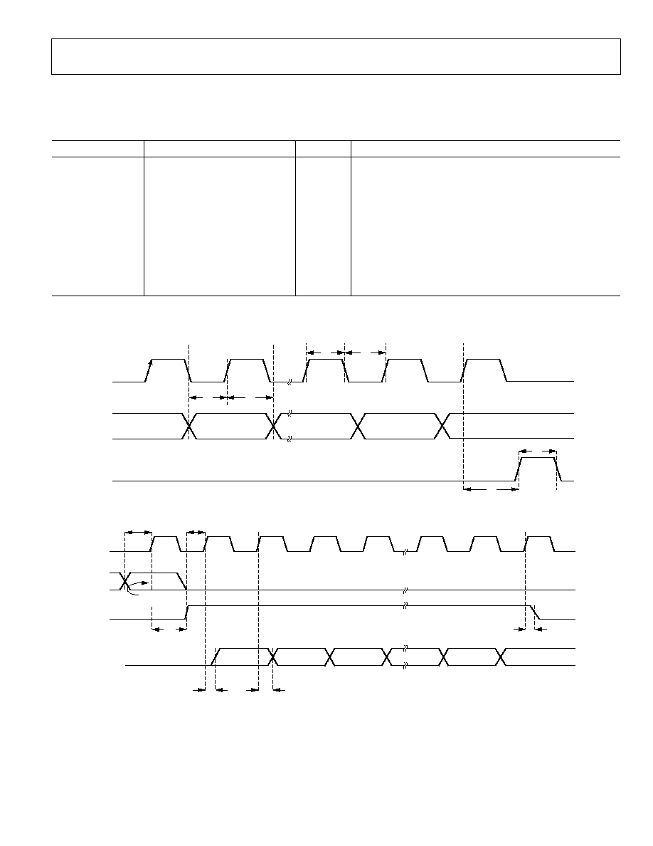
TIMING DIAGRAMS
SCLK
SLE
DB31 (MSB)
DB30
DB2
DB1
(CONTROL BIT C2)
SDATA
DB0 (LSB)
(CONTROL BIT C1)
t
6
t
1
t
2
t
3
t
4
t
5
05
54
2-
0
0
2
Figure 2. Serial Interface Timing Diagram
t
8
t
3
t
1
t
2
t
10
t
9
X
RV16
RV15
RV2
RV1
SCLK
SDATA
SLE
SREAD
REG7 DB0
(CONTROL BIT C1)
05
542
-
0
0
3
Figure 3. Readback Timing Diagram
ADF7025
Rev. A | Page 8 of 44
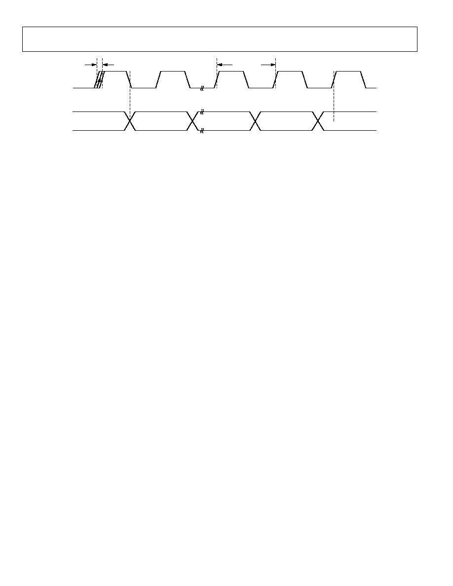
RxCLK
DATA
RxDATA
±1 × DATA RATE/32
1/DATA RATE
05
542
-
0
0
4
Figure 4. RxData/RxCLK Timing Diagram
ADF7025
Rev. A | Page 9 of 44
ABSOLUTE MAXIMUM RATINGS
T
A
= 25°C, unless otherwise noted.
Table 3.
Parameter Rating
V
DD
to GND
1
-0.3 V to +5 V
Analog I/O Voltage to GND
-0.3 V to AV
DD
+ 0.3 V
Digital I/O Voltage to GND
-0.3 V to DV
DD
+ 0.3 V
Operating Temperature Range
Industrial (B Version)
-40°C to +85°C
Storage Temperature Range
-65°C to +125°C
Maximum Junction Temperature
125°C
MLF
JA
Thermal Impedance
26°C/W
Lead Temperature Soldering
Vapor Phase (60 sec)
235°C
Infrared (15 sec)
240°C
1
GND = CPGND = RFGND = DGND = AGND = 0 V.
Stresses above those listed under Absolute Maximum Ratings
may cause permanent damage to the device. This is a stress
rating only; functional operation of the device at these or any
other conditions above those indicated in the operational
section of this specification is not implied. Exposure to absolute
maximum rating conditions for extended periods may affect
device reliability.
This device is a high performance, RF integrated circuit with an
ESD rating of <2 kV, and it is ESD sensitive. Proper precautions
should be taken for handling and assembly.
ESD CAUTION
ESD (electrostatic discharge) sensitive device. Electrostatic charges as high as 4000 V readily accumulate on
the human body and test equipment and can discharge without detection. Although this product features
proprietary ESD protection circuitry, permanent damage may occur on devices subjected to high energy
electrostatic discharges. Therefore, proper ESD precautions are recommended to avoid performance
degradation or loss of functionality.
ADF7025
Rev. A | Page 10 of 44
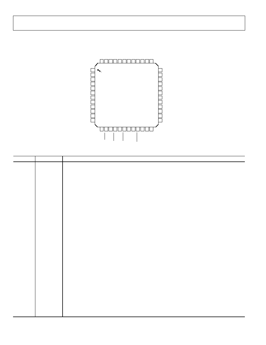
PIN CONFIGURATION AND FUNCTION DESCRIPTIONS
36
35
34
33
32
31
30
29
28
27
26
25
4
8
4
7
4
6
4
5
4
4
4
3
4
2
4
1
4
0
3
9
3
8
3
7
1
3
1
4
1
5
1
6
1
7
1
8
1
9
2
0
2
1
2
2
2
3
2
4
ADF7025
TOP VIEW
(Not to Scale)
VCOIN
VREG1
VDD1
RFOUT
RFGND
RFIN
RFINB
R
LNA
VDD4
RSET
VREG4
GND4
M
I
X
_
I
M
I
X
_
I
M
I
X
_
Q
M
I
X
_
Q
F
I
L
T
_
I
F
I
L
T
_
I
G
N
D
4
F
I
L
T
_
Q
F
I
L
T
_
Q
G
N
D
4
T
E
S
T
_
A
C
E
CLKOUT
DATA CLK
DATA I/O
INT/LOCK
VDD2
VREG2
ADCIN
GND2
SCLK
SREAD
SDATA
SLE
C
V
C
O
G
N
D
1
G
N
D
V
C
O
G
N
D
G
N
D
V
D
D
C
P
O
U
T
V
R
E
G
3
V
D
D
3
O
S
C
1
O
S
C
2
M
U
X
O
U
T
1
2
3
4
5
6
7
8
9
10
11
12
PIN 1
INDICATOR
0
55
42
-
0
0
6
Figure 5. Pin Configuration
Table 4. Pin Function Descriptions
Pin No.
Mnemonic
Description
1
VCOIN
The tuning voltage on this pin determines the output frequency of the voltage-controlled oscillator (VCO).
The higher the tuning voltage, the higher the output frequency.
2
VREG1
Regulator Voltage for PA Block. A 100 nF in parallel with a 5.1 pF capacitor should be placed between this pin
and ground for regulator stability and noise rejection.
3
VDD1
Voltage Supply for PA Block. Decoupling capacitors of 0.1 µF and 10 pF should be placed as close as possible
to this pin. All VDD pins should be tied together.
4
RFOUT
The modulated signal is available at this pin. Output power levels are from -20 dBm to +13 dBm. The output
should be impedance-matched to the desired load using suitable components. See the Transmitter section.
5
RFGND
Ground for Output Stage of Transmitter.
6
RFIN
LNA Input for Receiver Section. Input matching is required between the antenna and the differential LNA
input to ensure maximum power transfer. See the LNA/PA Matching section.
7
RFINB
Complementary LNA Input. See the LNA/PA Matching section.
8
R
LNA
External bias resistor for LNA. Optimum resistor is 1.1 k with 5% tolerance.
9
VDD4
Voltage supply for LNA/MIXER Block. This pin should be decoupled to ground with a 10 nF capacitor.
10
RSET
External Resistor to Set Charge Pump Current and Some Internal Bias Currents. Use 3.6 k with 5% tolerance.
11
VREG4
Regulator Voltage for LNA/MIXER Block. A 100 nF capacitor should be placed between this pin and GND
for regulator stability and noise rejection.
12
GND4
Ground for LNA/MIXER Block.
13 to 18
MIX/FILT
Signal Chain Test Pins. These pins are high impedance under normal conditions and should be left unconnected.
19, 22
GND4
Ground for LNA/MIXER Block.
20, 21, 23
FILT/TEST_A
Signal Chain Test Pins. These pins are high impedance under normal conditions and should be left unconnected.
24
CE
Chip Enable. Bringing CE low puts the ADF7025 into complete power-down. Register values are lost
when CE is low, and the part must be reprogrammed once CE is brought high.
25
SLE
Load Enable, CMOS Input. When LE goes high, the data stored in the shift registers is loaded into one
of the four latches. A latch is selected using the control bits.
26
SDATA
Serial Data Input. The serial data is loaded MSB first with the two LSBs as the control bits. This pin is
a high impedance CMOS input.
27
SREAD
Serial Data Output. This pin is used to feed readback data from the ADF7025 to the microcontroller.
The SCLK input is used to clock each readback bit (ADC readback) from the SREAD pin.
28
SCLK
Serial Clock Input. This serial clock is used to clock in the serial data to the registers. The data is latched
into the 24-bit shift register on the CLK rising edge. This pin is a digital CMOS input.

ADF7025
Rev. A | Page 11 of 44
Pin No.
Mnemonic
Description
29
GND2
Ground for Digital Section.
30
ADCIN
Analog-to-Digital Converter Input. The internal 7-bit ADC can be accessed through this pin.
Full scale is 0 V to 1.9 V. Readback is made using the SREAD pin.
31
VREG2
Regulator Voltage for Digital Block. A 100 nF in parallel with a 5.1 pF capacitor should be placed
between this pin and ground for regulator stability and noise rejection.
32
VDD2
Voltage Supply for Digital Block. A decoupling capacitor of 10 nF should be placed as close as possible
to this pin.
33
INT/LOCK
Bidirectional Pin. In output mode (interrupt mode), the ADF7025 asserts the INT/LOCK pin when
it has found a match for the preamble sequence.
In input mode (lock mode), the microcontroller can be used to lock the demodulator threshold
when a valid preamble has been detected. Once the threshold is locked, NRZ data can be reliably received.
In this mode, a demodulator lock can be asserted with minimum delay.
34
DATA I/O
Transmit Data Input/Received Data Output. This is a digital pin, and normal CMOS levels apply.
35
DATA CLK
In receive mode, the pin outputs the synchronized data clock. The positive clock edge is matched to the
center of the received data.
36
CLKOUT
A Divided-Down Version of the Crystal Reference with Output Driver. The digital clock output can be used
to drive several other CMOS inputs, such as a microcontroller clock. The output has a 50:50 mark-space ratio.
37
MUXOUT
This pin provides the lock_detect signal, which is used to determine if the PLL is locked to the correct
frequency. Other signals include regulator_ready, which is an indicator of the status of the serial interface
regulator.
38
OSC2
The reference crystal should be connected between this pin and OSC1. A TCXO reference can be used by
driving this pin with CMOS levels and disabling the crystal oscillator.
39
OSC1
The reference crystal should be connected between this pin and OSC2.
40
VDD3
Voltage Supply for the Charge Pump and PLL Dividers. This pin should be decoupled to ground
with a 0.01 µF capacitor.
41 VREG3 Regulator Voltage for Charge Pump and PLL Dividers. A 100 nF in parallel with a 5.1 pF capacitor
should be placed between this pin and ground for regulator stability and noise rejection.
42
CPOUT
Charge Pump Output. This output generates current pulses that are integrated in the loop filter.
The integrated current changes the control voltage on the input to the VCO.
43
VDD
Voltage Supply for VCO Tank Circuit. This pin should be decoupled to ground with a 0.01 µF capacitor.
44 to 47
GND
Grounds for VCO Block.
48
CVCO
A 22 nF capacitor should be placed between this pin and VREG1 to reduce VCO noise.
ADF7025
Rev. A | Page 12 of 44
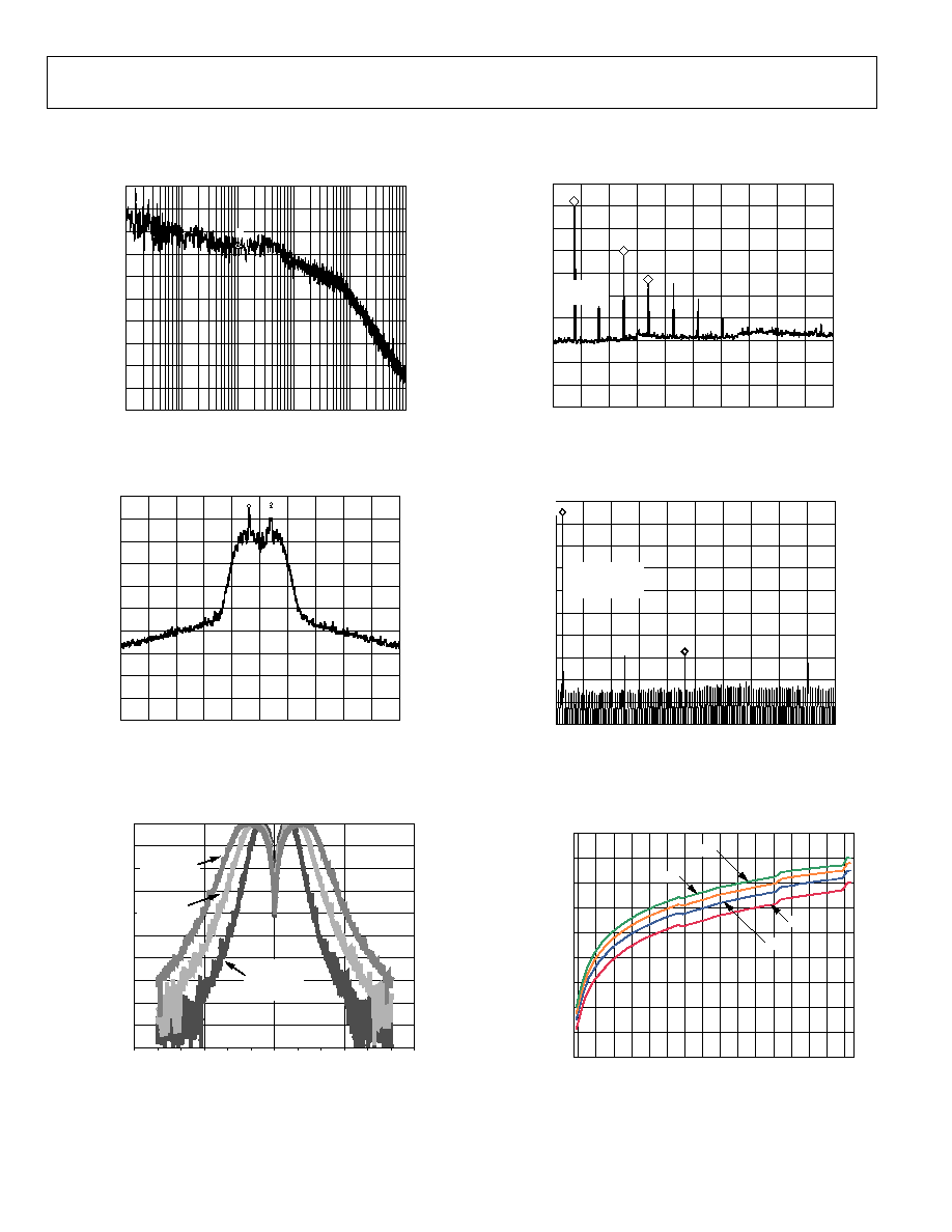
TYPICAL PERFORMANCE CHARACTERISTICS
100Hz
10Hz
05
54
2-
0
0
7
FREQUENCY OFFSET
CARRIER POWER 6.11dBm
REF 60dBc/Hz 10.00dB/
ATTEN 2.00dB MKR1
10.00KHz
88.46dBc/Hz
1
Figure 6. Phase Noise Response at 915 MHz, V
DD
= 3.0 V, ICP = 0.867 mA
CENTER 915.00MHz
#RES BW 10kHz
VBW 10kHz
SPAN 5MHz
SWEEP 60.32ms (601pts)
05
54
2-
00
8
REF 10dBm
NORM LOG 10dB/
ATTEN 20dB
MKR1 400Hz
0.69dB
1
1R
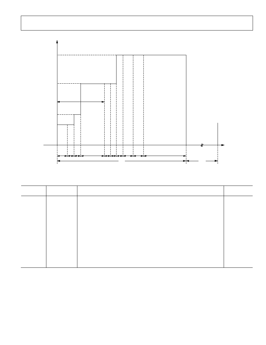
Figure 7. Output Spectrum in FSK Modulation (915 MHz,
172.8 kbps Data Rate, 200 kHz Frequency Deviation)
1500 1200
600 300
300
600
1200 1500
0
50
1800
900
0
900
1800
FREQUENCY (KHz)
ATT
E
N
U
A
TI
ON
L
EVEL
(
d
B
)
45
40
35
30
25
20
15
10
5
±600KHz
FILTER B/W
±450KHz
FILTER B/W
±300KHz
FILTER B/W
05
54
2-
00
9
Figure 8. Baseband Filter Response
STOP 10.000GHz
SWEEP 16.52ms (601pts)
MKR4 3.482GHz
SWEEP 16.52ms (601pts)
START 100MHz
RES BW 3MHz
REF 10dBm
PEAK
LOG
10dB/
VBW 3MHz
ATTEN 20dB
1
3
4
REF LEVEL
10.00dBm
05
542
-
0
1
0
Figure 9. Harmonic Response, RFOUT Matched to 50 , No Filter
STOP 5.000GHz
SWEEP 5.627s (601pts)
Mkr1 1.834GHz
62.57dB
START 800MHz
#RES BW 30kHz
REF 15dBm
ATTEN 30dB
VBW 30kHz
NORM
LOG
10dB/
LgAv
W1S2
S3FC
AA
£(f):
FTun
Swp
1R
1
MARKER
1.834000000GHz
62.57dB
05
54
2-
0
1
1
Figure 10. Harmonic Response, Murata Dielectric Filter
PA SETTING
1
5
9 13 17 21 25 29 33 37 41 45 49 53 57 61
P
A
OU
T
P
U
T
P
O
W
E
R
20
10
15
0
5
10
5
20
15
25
11µA
9µA
5µA
7µA
055
42
-
0
5
3
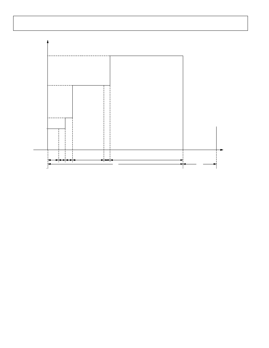
Figure 11. PA Output Power vs. Setting
ADF7025
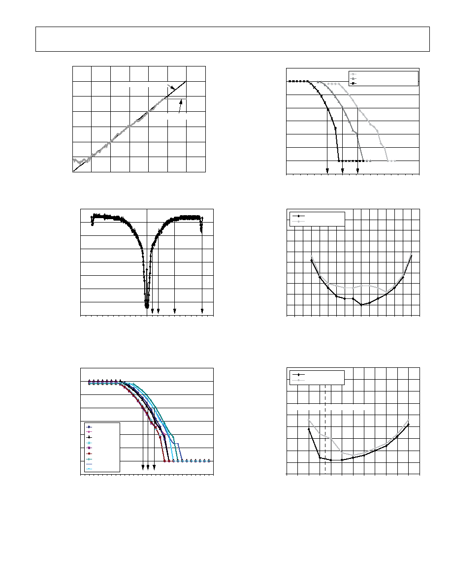
Rev. A | Page 13 of 44
05
54
2-
0
1
4
20
120
100
80
60
40
20
0
20
20
60
0
40
80
100
120
ACTUAL INPUT LEVEL
RSSI READBACK LEVEL
RF I/P (dB)
RS
S
I
L
E
V
E
L
(
d
B)
Figure 12. Digital RSSI Readback
10
0
10
20
30
40
50
60
70
12
6
0
6
12
05
54
2-
0
1
3
OFFSET OF INTERFERER FROM WANTED SIGNAL (MHz)
LEV
E
L
O
F R
E
J
E
C
TI
ON
(
d
B
)
Figure 13. Wideband Interference Rejection;
Wanted Signal (901 MHz, 38.4 kbps Data Rate, 200 kHz Frequency
Deviation) at 6 dB Above Sensitivity Point; Interferer = CW Jammer
05
54
2-
0
1
5
RF I/P LEVEL (dBm)
BE
R
8
7
6
5
4
3
2
1
0
115
110
105
100
95
90
85
2.3V, +25°C
3V, +25°C
3.6V, +25°C
2.3V, 40°C
3V, 40°C
3.6V, 40°C
2.3V, +85°C
3V, +85°C
3.6V, +85°C
Figure 14. Sensitivity vs. V
DD
and Temperature
(172.8 kbps Data Rate, 200 kHz Frequency Deviation,
Baseband Bandwidth ±600 kHz)
8
7
6
5
4
3
2
1
0
116
108
100
90
78
055
42
-
0
1
6
RF I/P LEVEL (dBm)
LOG
(
B
E
R
)
DATA RATE = 384k, FDEV = 450k
DATA RATE = 172k, FDEV = 200k
DATA RATE = 38.4k, FDEV = 200k
Figure 15. BER vs. Data Rate (Combined Matching Network)
05
54
2-
0
1
7
DEVIATION FREQUENCY (kHz)
S
E
NS
IT
I
V
IT
Y
P
O
I
NT
(
d
Bm)
= CORRELATOR
= LINEAR
100
95
90
85
80
75
70
65
60
55
50
0
50 100 150 200 250 300 350 400 450 500 550 600 650 700 750 800
Figure 16. Sensitivity vs. Mod Index (Data Rate = 384 kbps, Baseband
Filter Bandwidth = ±600 kHz), for Both Demodulator Types
105
100
95
90
85
80
75
70
65
60
0
50
100 150 200 250 300 350 400 450 500 550 600
05
54
2-
0
1
8
DEVIATION FREQUENCY (kHz)
SEN
SI
T
I
VI
T
Y
P
O
I
N
T
(
d
B
m
)
= CORRELATOR
= LINEAR
= CORRELATOR
= LINEAR
BB BW = ±450kHz BB BW = ±600kHz
Figure 17. Sensitivity vs. Mod Index (Data Rate = 172.8 kbps),
for Both Demodulator Types
ADF7025
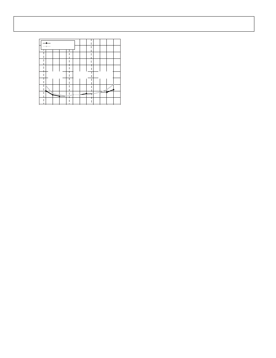
Rev. A | Page 14 of 44
110
105
100
95
90
85
80
75
70
65
60
0
50 100 150 200 250 300 350 400 450 500 550 600
05
54
2-
0
5
2
DEVIATION FREQUENCY (kHz)
S
E
NS
IT
I
V
IT
Y
P
O
I
NT
(
d
Bm)
= CORRELATOR
= LINEAR
BB BW =
±300kHz
BB BW =
±450kHz
BB BW =
±600kHz
Figure 18. Sensitivity vs. Mod Index (Data Rate = 38.4 kbps),
for both Demodulator Types
ADF7025
Rev. A | Page 15 of 44
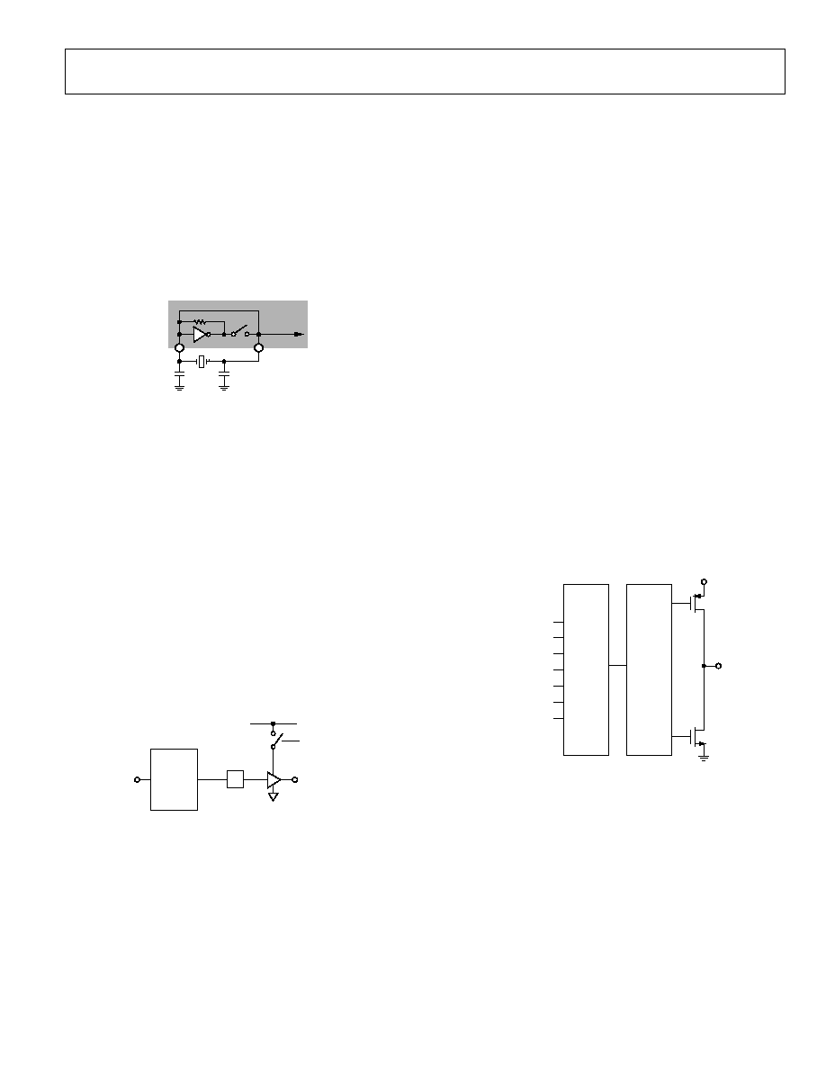
FREQUENCY SYNTHESIZER
REFERENCE INPUT SECTION
The on-board crystal oscillator circuitry (see Figure 19) can use
an inexpensive quartz crystal as the PLL reference. The oscillator
circuit is enabled by setting R1_DB12 high. It is enabled by
default on power-up and is disabled by bringing CE low. Errors
in the crystal can be corrected by adjusting the Fractional-N
value (see the N Counter section). A single-ended reference
(TCXO, CXO) can also be used. The CMOS levels should be
applied to OSC2 with R1_DB12 set low.
OSC1
CP1
CP2
OSC2
0
554
2-
0
1
9
Figure 19. Oscillator Circuit on the ADF7025
Two parallel resonant capacitors are required for oscillation at
the correct frequency; their values are dependent on the crystal
specification. They should be chosen so that the series value of
capacitance added to the PCB track capacitance adds up to the
load capacitance of the crystal, usually 20 pF. Track capacitance
values vary from 2 pF to 5 pF, depending on board layout.
Where possible, choose capacitors that have a very low
temperature coefficient to ensure stable frequency operation
over all conditions.
CLKOUT Divider and Buffer
The CLKOUT circuit takes the reference clock signal from the
oscillator section, shown in Figure 19, and supplies a divided-
down 50:50 mark-space signal to the CLKOUT pin. An even
divide from 2 to 30 is available. This divide number is set in
R1_DB [8:11]. On power-up, the CLKOUT defaults to
divide-by-8.
DV
DD
CLKOUT
ENABLE BIT
CLKOUT
OSC1
DIVIDER
1 TO 15
÷2
05
542
-
0
2
0
Figure 20. CLKOUT Stage
To disable CLKOUT, set the divide number to 0. The output
buffer can drive up to a 20 pF load with a 10% rise time at
4.8 MHz. Faster edges can result in some spurious feedthrough
to the output. A small series resistor (50 ) can be used to slow
the clock edges to reduce these spurs at F
CLK
.
R Counter
The 3-bit R counter divides the reference input frequency by an
integer from 1 to 7. The divided-down signal is presented as the
reference clock to the phase frequency detector (PFD). The divide
ratio is set in Register 1. Maximizing the PFD frequency reduces
the N value. This reduces the noise multiplied at a rate of 20 log(N)
to the output, as well as reducing occurrences of spurious
components. The R register defaults to R = 1 on power-up.
PFD [Hz] = XTAL/R
MUXOUT and Lock Detect
The MUXOUT pin allows the user to access various digital
points in the ADF7025. The state of MUXOUT is controlled by
Bits R0_DB [29:31].
Regulator Ready
Regulator ready is the default setting on MUXOUT after the
transceiver has been powered up. The power-up time of the
regulator is typically 50 µs. Because the serial interface is powered
from the regulator, the regulator must be at its nominal voltage
before the ADF7025 can be programmed. The status of the
regulator can be monitored at MUXOUT. When the
regulator_ready signal on MUXOUT is high, programming of
the ADF7025 can begin.
REGULATOR READY
DIGITAL LOCK DETECT
ANALOG LOCK DETECT
R COUNTER OUTPUT
N COUNTER OUTPUT
PLL TEST MODES
- TEST MODES
MUX
CONTROL
DGND
DV
DD
MUXOUT
0
55
42
-
0
2
1
Figure 21. MUXOUT Circuit
Digital Lock Detect
Digital lock detect is active high. The lock detect circuit is
located at the PFD. When the phase error on five consecutive
cycles is less than 15 ns, lock detect is set high. Lock detect
remains high until a 25 ns phase error is detected at the PFD.
Because no external components are needed for digital lock
detect, it is more widely used than analog lock detect.
ADF7025
Rev. A | Page 16 of 44
Analog Lock Detect
This N-channel open-drain lock detect should be operated with
an external pull-up resistor of 10 k nominal. When a lock has
been detected, this output is high with narrow low-going pulses.
Voltage Regulators
The ADF7025 contains four regulators to supply stable voltages
to the part. The nominal regulator voltage is 2.3 V. Each regulator
should have a 100 nF capacitor connected between VREG and
GND. When CE is high, the regulators and other associated
circuitry are powered on, drawing a total supply current of 2 mA.
Bringing the chip-enable pin low disables the regulators,
reduces the supply current to less than 1 µA, and erases all
values held in the registers. The serial interface operates from
a regulator supply; therefore, to write to the part, the user must
have CE high and the regulator voltage must be stabilized.
Regulator status (VREG4) can be monitored using the regulator
ready signal from MUXOUT.
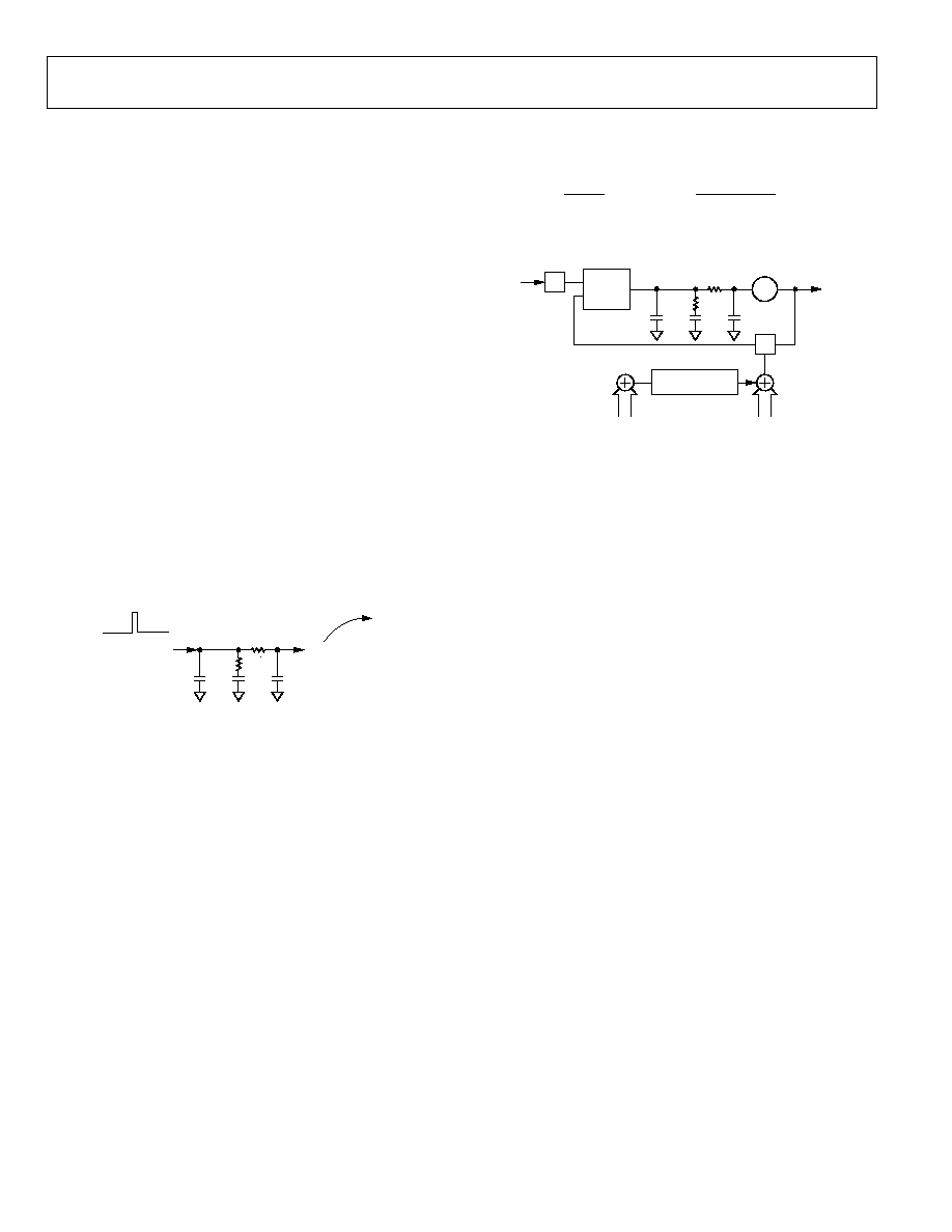
Loop Filter
The loop filter integrates the current pulses from the charge
pump to form a voltage that tunes the output of the VCO to the
desired frequency. It also attenuates spurious levels generated by
the PLL. A typical loop filter design is shown in Figure 22.
CHARGE
PUMP OUT
VCO
05
54
2-
0
2
2
Figure 22. Typical Loop Filter Configuration
In general, a loop filter bandwidth (LBW) of between the data
rate and twice the data rate is recommended. Widening the
LBW excessively reduces the time spent jumping between
frequencies, but it can cause insufficient spurious attenuation.
Narrow-loop bandwidths can result in the loop taking long
periods of time to attain lock. For the ADF7025 in receive mode,
the loop filter bandwidth affects the close-in blocking perform-
ance. The narrower the bandwidth of the loop filter, the greater
the close-in interference resilience of the receiver.
Careful design of the loop filter is critical to obtaining accurate
FSK modulation. The free design tool ADIsimPLL can be used
to design loop filters for the ADF7025.
N Counter
The feedback divider in the ADF7025 PLL consists of an 8-bit
integer counter and a 14-bit - Fractional-N divider. The
integer counter is the standard pulse-swallow type common in
PLLs. This sets the minimum integer divide value to 31.
The fractional divide value gives very fine resolution at the
output, where the output frequency of the PLL is calculated as
)
2
(
15
N
Fractional
N
Integer
R
XTAL
F
OUT
+
×
=
VCO
4N
THIRD-ORDER
- MODULATOR
PFD/
CHARGE
PUMP
4R
INTEGER-N
FRACTIONAL-N
REFERENCE IN
05
54
2-
0
2
3
Figure 23. Fractional-N PLL
The combination of the Integer-N (maximum = 255) and the
Fractional-N (maximum = 16383/16384) gives a maximum N
divider of 255 + 1. Therefore, the minimum usable PFD is
PDF
MIN
[Hz] = Maximum Required Output Frequency/(255 + 1)
For example, when operating in the European 868 MHz to
870 MHz band, PFD
MIN
equals 3.4 MHz.
Voltage Controlled Oscillator
To minimize spurious emissions, the on-chip VCO operates
from 1732 MHz to 1856 MHz. The VCO signal is then divided
by 2 to give the required frequency for the transmitter and the
required LO frequency for the receiver.
The VCO should be re-centered, depending on the required
frequency of operation, by programming the VCO adjust bits
R1_DB [20:21].
For operation in the 862 MHz to 870 MHz band, it is recom-
mended to use a VCO bias of at least Setting 10 and to set the
VCO adjust bit to Setting 0. For operation in the 902 MHz to
928 MHz band, it is recommended to use a VCO bias of at least
Setting 12 and to set the VCO adjust bit to Setting 3. This is to
ensure correct operation under all conditions.
The VCO is enabled as part of the PLL by the PLL-enable bit,
R0_DB28.
An additional frequency divide-by-2 is included to allow
operation in the lower 431 MHz to 464 MHz bands. To enable
operation in these bands, R1_DB13 should be set to 1. The
VCO needs an external 22 nF between the VCO and the
regulator to reduce internal noise.
ADF7025
Rev. A | Page 17 of 44
VCO Bias Current
VCO bias current can be adjusted using Bit R1_DB19 to
Bit R1_DB16. To ensure VCO oscillation under all conditions,
the minimum bias current setting is Setting 12 (0xC).
431 MHz to 464 MHz Operation
For operation in the 431 MHz to 464 MHz band, the frequency
divide-by-2 has to be enabled. It is enabled by R1_DB13. Because
this divide is external to the synthesizer loop, the feedback
divider number (N + F) should be programmed to a value twice
the desired RF output frequency.
VCO
LOOP FILTER
MUX
VCO SELECT BIT
TO PA AND
N DIVIDER
VCO BIAS
R1_DB (16:19)
220µF
CVCO PIN
÷2
÷2
05
542
-
0
2
4
Figure 24. Voltage Controlled Oscillator
CHOOSING CHANNELS FOR BEST SYSTEM
PERFORMANCE
The Fractional-N PLL allows the selection of any channel
within 862 MHz to 928 MHz (and 431 MHz to 464 MHz using
divide-by-2) to a resolution of <300 Hz. This also facilitates
frequency-hopping systems.
Careful selection of the RF transmit channels must be made to
achieve best spurious performance. The architecture of
Fractional-N results in some level of the nearest integer channel
moving through the loop to the RF output. These beat-note
spurs are not attenuated by the loop, if the desired RF channel
and the nearest integer channel are separated by a frequency of
less than the LBW.
The occurrence of beat-note spurs is rare, because the integer
frequencies are at multiples of the reference, which is typically
>10 MHz.
Beat-note spurs can be significantly reduced in amplitude by
avoiding very small or very large values in the fractional
register, using the frequency doubler. By having a channel
1 MHz away from an integer frequency, a 100 kHz loop filter
can reduce the level to less than -45 dBc.
ADF7025
Rev. A | Page 18 of 44
TRANSMITTER
RF OUTPUT STAGE
The PA of the ADF7025 is based on a single-ended, controlled
current, open-drain amplifier that has been designed to deliver
up to 13 dBm into a 50 load at a maximum frequency of
928 MHz.
The PA output current and, consequently, the output power are
programmable over a wide range. The PA configuration is
shown in Figure 25. The output power is independent of the
state of the DATA I/O pin. The output power is set using Bits
R2_DB [9:14].
IDAC
2
6
R2_DB(9:14)
R2_DB4
R2_DB5
DIGITAL
LOCK DETECT
R2_DB(30:31)
+
RFGND
RFOUT
FROM VCO
05
54
2-
0
2
5
Figure 25. PA Configuration
The PA is equipped with overvoltage protection, which makes it
robust in severe mismatch conditions. Depending on the
application, one can design a matching network for the PA to
exhibit optimum efficiency at the desired radiated output power
level for a wide range of different antennas, such as loop or
monopole antennas. See the LNA/PA Matching section for
details.
PA Bias Currents
Control Bits R2_DB [30:31] facilitate an adjustment of the PA
bias current to further extend the output power control range, if
necessary. If this feature is not required, the default value of
7 µA is recommended. The output stage is powered down by
resetting Bit R2_DB4.
MODULATION SCHEME
Frequency Shift Keying (FSK)
Frequency shift keying is implemented by setting the N value for
the center frequency and then toggling this with the TxData
line. The deviation from the center frequency is set using
Bits R2_DB [15:23]. The deviation from the center frequency in
Hz is
14
2
[Hz]
Number
Modulation
PFD
FSK
DEVIATION
×
=
where Modulation Number is a number from 1 to 511
(R2_DB(15:23)).
Select FSK using Bits R2_DB [6:8].
VCO
÷N
THIRD-ORDER
- MODULATOR
PFD/
CHARGE
PUMP
4R
INTEGER-N
FRACTIONAL-N
PA STAGE
F
DEV
+F
DEV
TxDATA
FSK DEVIATION
FREQUENCY
05
54
2-
0
2
6
Figure 26. FSK Implementation
Modulation Index
The choice of deviation frequency for a given data rate is critical
to get optimum sensitivity performance from the ADF7025.
The modulation index (MI) of an FSK modulated signal is
defined as
[bps]
[Hz]
2
Rate
Data
Deviation
Frequency
MI
×
=
It is recommended to use a MI > 1 for the ADF7025. The
variation of receiver sensitivity with modulation index, for
various data rates, can be observed in Figure 16, Figure 17,
and Figure 18.
ADF7025
Rev. A | Page 19 of 44
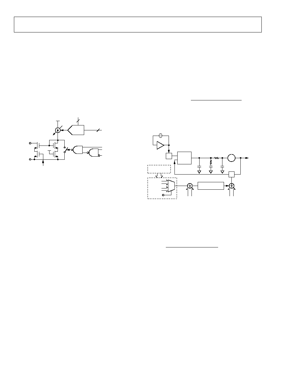
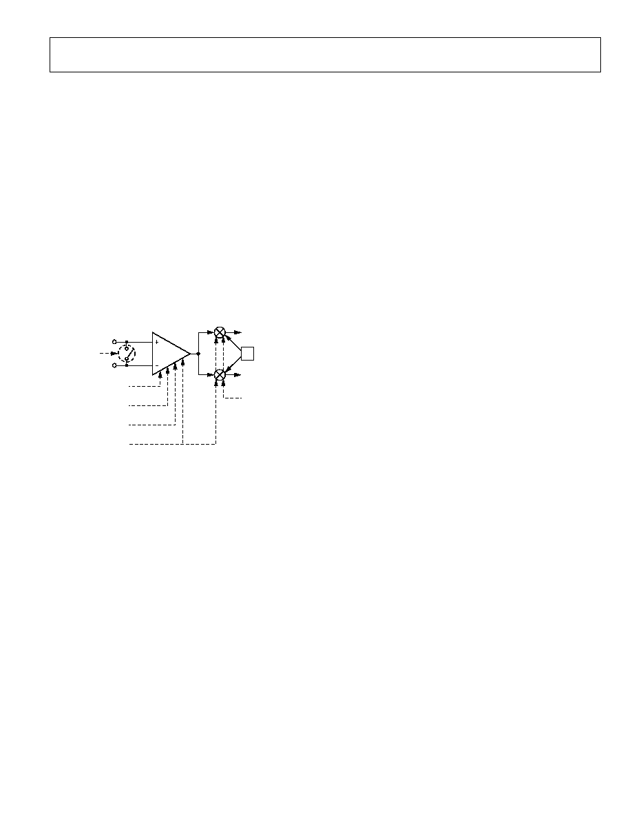
RECEIVER
RF FRONT END
The ADF7025 is based on a fully integrated, zero-IF receiver
architecture. The zero-IF architecture minimizes power
consumption and the external component count while avoiding
the need for image rejection.
Figure 27 shows the structure of the receiver front end. The
numerous programming options allow users to trade off
sensitivity, linearity, and current consumption against each
other in the way best suitable for their applications. To achieve a
high level of resilience against spurious reception, the LNA
features a differential input. Switch SW2 shorts the LNA input
when transmit mode is selected (R0_DB27 = 0). This feature
facilitates the design of a combined LNA/PA matching network,
avoiding the need for an external Rx/Tx switch. See the
LNA/PA Matching section for details on the design of the
matching network.
SW2
LNA
RFIN
RFINB
Tx/Rx SELECT
[R0_DB27]
LNA MODE
[R6_DB15]
LNA CURRENT
[R6_DB(16:17)]
MIXER LINEARITY
[R6_DB18]
LO
I (TO FILTER)
Q (TO FILTER)
LNA GAIN
[R9_DB(20:21)]
LNA/MIXER ENABLE
[R8_DB6]
05
542-
027
Figure 27. ADF7025 RF Front End
The LNA is followed by a quadrature downconversion mixer,
which converts the RF signal direct to baseband. The output
frequency of the synthesizer must be programmed to the value
equal to the center frequency of the received channel.
The LNA has two basic operating modes: high gain/low noise
mode and low gain/low power mode. To switch between the
two modes, use the LNA_mode bit, R6_DB15. The mixer is also
configurable between a low current and an enhanced linearity
mode using the mixer_linearity bit, R6_DB18.
Based on the specific sensitivity and linearity requirements of
the application, it is recommended to adjust control bits
LNA_mode (R6_DB15) and mixer_linearity (R6_DB18).
The gain of the LNA is configured by the LNA_gain field,
R9_DB [20:21] and can be set by either the user or the
automatic gain control (AGC) logic.
Filter Settings/Calibration
Out-of-band interference is rejected by means of a fifth-order,
low-pass filter (LPF). The bandwidth of the filter can be
programmed to be ±300 kHz, ±450 kHz, or ±600 kHz by means
of Control Bits R1_DB [22:23] and should be chosen as a
compromise between interference rejection and attenuation of
the desired signal. A high-pass filter is also included as part of
the low-pass filter to prevent against dc offset problems. The
bandwidth of this filter is ~60 kHz. To avoid significant loss of
FSK modulated signal in the filter, the frequency deviation
needs to be significantly larger than this pole (refer to the
Modulation Index section). The minimum allowable frequency
deviation is 100 kHz.
To compensate for manufacturing tolerances, the LPF should
be calibrated once after power-up. The LPF calibration logic
requires that the LPF divider in Bits R6_DB [20:28] be set
depending on the crystal frequency. Once initiated by setting
Bit R6_DB19, the calibration is performed automatically
without any user intervention. The calibration time is 200 µs,
during which the ADF7025 should not be accessed. It is
important not to initiate the calibration cycle before the crystal
oscillator has fully settled. If the AGC loop is disabled, the gain
of LPF can be set to three levels using the filter_gain field,
R9_DB [20:21]. The filter gain is adjusted automatically, if the
AGC loop is enabled.
ADF7025
Rev. A | Page 20 of 44
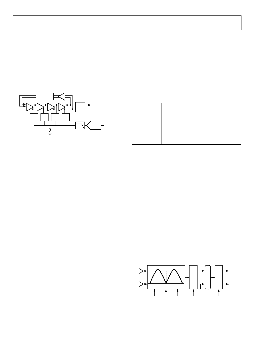
RSSI/AGC
The RSSI is implemented as a successive compression log amp
following the baseband channel filtering. The log amp achieves
±3 dB log linearity. It also doubles as a limiter to convert the
signal-to-digital levels for the FSK demodulator. Offset
correction is achieved using a switched capacitor integrator in
feedback around the log amp. This uses the BB offset clock
divide. The RSSI level is converted for user readback and
digitally controlled AGC by an 80-level (7-bit) flash ADC. This
level can be converted to input power in dBm.
1
IFWR
IFWR
IFWR
IFWR
LATCH
A
A
A
R
CLK
ADC
OFFSET
CORRECTION
RSSI
DEMOD
FSK
DEMOD
05
542
-
0
2
8
Figure 28. RSSI Block Diagram
Offset Correction Clock
In Register 3, the user should set the BB offset clock divide bits
R3_DB [4:5] to give an offset clock between 1 MHz and 2 MHz,
where BBOS _CLK [Hz] = XTAL/(BBOS_CLK_DIVIDE).
BBOS_CLK_DIVIDE can be set to 4, 8, or 16.
AGC Information
In Register 9, the user should select automatic gain control by
selecting Auto In R9_DB18 and Auto In R9_DB19. The user
should then program AGC Low Threshold R9_DB [4:10] and
AGC High Threshold R9_DB [11:17]. The default values for the
low and high thresholds are 30 and 70, respectively; however,
these are not the optimum settings for all operating conditions.
The recommended values for the low and high thresholds are
15 and 79, respectively. In the AGC 2 register (Register 10), the
user should program the AGC delay to be long enough to allow
the loop to settle. The default/recommended value is 10.
XTAL
DIVIDE
CLK
SEQ
DELAY
AGC
Time
Wait
AGC
_
_
_
_
_
×
=
AGC Settling = AGC_Wait_Time × Number of Gain Changes
Thus, in the worst case, if the AGC loop has to go through all five
gain changes, AGC delay = 10, and SEQ_CLK = 200 kHz, then
AGC settling = 10 × 5 µs × 5 = 250 s. Minimum AGC_Wait_Time
must be at least 25 µs.
RSSI Formula (Converting to dBm)
Input_Power [dBm] = -98 dBm + (Readback_Code +
Gain_Mode_Correction ) × 0.5
where:
Readback_Code is given by Bit RV7 to Bit RV1 in the readback
register (see the Readback Format section).
Gain_Mode_Correction is given by the values in Table 5.
LNA gain and filter gain (LG2/LG1, FG2/FG1) are also
obtained from the readback register.
Table 5. Gain Mode Correction
LNA Gain
(LG2, LG1)
Filter Gain
(FG2, FG1)
Gain Mode Correction
H (11)
H (10)
0
M (10)
H (10)
17
M (10)
M (01)
53
M (10)
L (00)
65
L (01)
L (00)
90
EL (00)
L (00)
113
These numbers are for an unmodulated tone. For a modulated
signal, the RSSI readback may have to be adjusted to get the
required accuracy. An additional factor should also be
introduced to account for losses in the front-end matching
network/antenna.
FSK DEMODULATORS ON THE ADF7025
The two FSK demodulators on the ADF7025 are
·
FSK correlator/demodulator
·
Linear demodulator
Select these using the Demod Select Bits R4_DB [4:5].
FSK CORRELATOR/DEMODULATOR
The quadrature outputs of the IF filter are first limited and then
fed to a pair of digital frequency correlators that perform band-
pass filtering of the binary FSK frequencies at (IF + F
DEV
) and
(IF - F
DEV
). Data is recovered by comparing the output levels
from each of the two correlators. The performance of this
frequency discriminator approximates that of a matched filter
detector, which is known to provide optimum detection in the
presence of AWGN.
PO
ST
DE
M
O
D F
I
L
T
E
R
DA
T
A
S
Y
NCHRO
NI
Z
E
R
F
DEV
+ F
DEV
I
0
Q
LIMITERS
0
DB(4:13)
DB(8:15)
DB(14)
Rx DATA
Rx CLK
SLICER
FREQUENCY CORRELATOR
+
0
5
542-
0
2
9
Figure 29. FSK Correlator/Demodulator Block Diagram

ADF7025
Rev. A | Page 21 of 44
Postdemodulator Filter
A second-order, digital low-pass filter removes excess noise
from the demodulated bit stream at the output of the
discriminator. The bandwidth of this postdemodulator filter is
programmable and must be optimized for the user's data rate. If
the bandwidth is set too narrow, performance is degraded due
to intersymbol interference (ISI). If the bandwidth is set too
wide, excess noise degrades the receiver's performance.
Typically, the 3 dB bandwidth of this filter is set at approximately
0.75 times the user's data rate, using Bits R4_DB [6:15].
Bit Slicer
The received data is recovered by the threshold detecting the
output of the postdemodulator low-pass filter. In the correlator/
demodulator, the binary output signal levels of the frequency
discriminator are always centered on 0. Therefore, the slicer
threshold level can be fixed at 0, and the demodulator
performance is independent of the run-length constraints of the
transmit data bit stream. This results in robust data recovery,
which does not suffer from the classic baseline wander
problems that exist in more traditional FSK demodulators.
Data Synchronizer
An oversampled digital PLL is used to resynchronize the received
bit stream to a local clock. The oversampled clock rate of the
PLL (CDR_CLK) must be set at 32 times the data rate. See the
Register 3--Receiver Clock Register section for a definition of
how to program. The clock recovery PLL can accommodate
frequency errors of up to ±2%.
FSK Correlator Register Settings
To enable the FSK correlator/demodulator, Bits R4_DB [5:4]
should be set to 01. To achieve best performance, the bandwidth
of the FSK correlator must be optimized for the specific deviation
frequency that is used by the FSK transmitter.
The discriminator BW is controlled in Register 6 by
R6_DB [4:13] and is defined as
Discriminator_BW = DEMOD_CLK/(4 × F
DEV
)
where:
DEMOD_CLK is as defined in the Register 3--Receiver Clock
Register section.
F
DEV
is the deviation from the carrier frequency in FSK
modulation.
Postdemodulator Bandwidth Register Settings
The 3 dB bandwidth of the postdemodulator filter is controlled
by Bits R4_ DB [6:15] and is given by
CLK
_
DEMOD
F
Setting
_
BW
_
Demod
_
Post
CUTOFF
×
×
=
2
2
10
where F
CUTOFF
is the target 3 dB bandwidth in Hz of the post-
demodulator filter. This should typically be set to 0.75 times
the data rate (DR).
Some sample settings for the FSK correlator/demodulator are
DEMOD_CLK = 11.0592 MHz
DR = 200 kbps
F
DEV
= 300 kHz
Therefore,
F
CUTOFF
= 0.75 × 200 × 10
3
Hz
Post_Demod_BW = 2
11
× × 150 × 10
3
Hz/(11.0592 MHz)
Post_Demod_BW = Round (87.266) = 87
and
Discriminator_BW = (11.0592 MHz )/(4 × 300 × 10
3
) =
9.21 = 9 (rounded to the nearest integer)
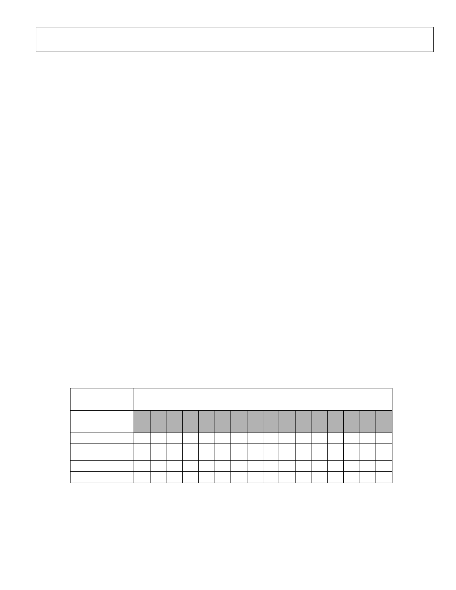
Table 6. Register Settings
Setting Name
Register Address
Value
Post_Demod_BW R4_DB
[6:15]
0x09
Discriminator BW
R6_DB [4:13]
0x58
ADF7025
Rev. A | Page 22 of 44
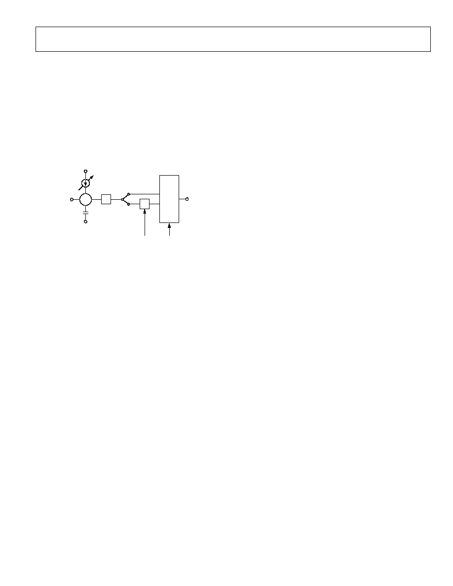
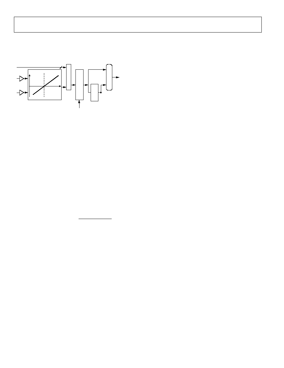
LINEAR FSK DEMODULATOR
A block diagram of the linear FSK demodulator is shown in
Figure 30.
A
V
E
RAG
I
N
G
FI
L
T
E
R
EN
V
E
L
O
PE
DE
T
E
C
T
O
R
SLICER
FREQ
0Hz
LEVEL
I
Q
LIMITER
7
MUX 1
ADC RSSI OUTPUT
LINEAR DISCRIMINATOR
DB(6:15)
Rx DATA
+
05
54
2-
03
0
Figure 30. Block Diagram of Linear FSK Demodulator
This method of frequency demodulation is useful when very
short preamble length is required.
A digital frequency discriminator provides an output signal that
is linearly proportional to the frequency of the limiter outputs.
The discriminator output is then filtered and averaged using a
combined averaging filter and envelope detector. The demodu-
lated FSK data is recovered by threshold-detecting the output of
the averaging filter, as shown in Figure 30. In this mode, the
slicer output shown in Figure 30 is routed to the data synchro-
nizer PLL for clock synchronization. To enable the linear FSK
demodulator, Bits R4_DB [4:5] are set to [00].
The 3 dB bandwidth of the postdemodulation filter is set in the
same way as the FSK correlator/demodulator, which is set in
R4_DB(6:15) and is defined as
CLK
DEMOD
F
Setting
BW
Demod
Post
CUTOFF
_
2
2
_
_
_
10
×
×
=
where:
F
CUTOFF
is the target 3 dB bandwidth in Hz of the
postdemodulator filter.
DEMOD_CLK is as defined in the Register 3--Receiver Clock
Register section.
AUTOMATIC SYNC WORD RECOGNITION
The ADF7025 also supports automatic detection of the sync or
ID fields. To activate this mode, the sync (or ID) word must be
preprogrammed into the ADF7025. In receive mode, this
preprogrammed word is compared to the received bit stream
and, when a valid match is identified, the external pin
INT/LOCK is asserted by the ADF7025.
This feature can be used to alert the microprocessor that a valid
channel has been detected. It relaxes the computational require-
ments of the microprocessor and reduces the overall power
consumption. The INT/LOCK is automatically de-asserted
again after nine data clock cycles.
The automatic sync/ID word detection feature is enabled by
selecting Demod Mode 2 or Demod Mode 3 in the demodulator
setup register. Do this by setting R4_DB [25:23] = [010] or
R4_DB [25:23] = [011]. Bits R5_DB [4:5] are used to set the
length of the sync/ID word, which can be either 12 bits, 16 bits,
20 bits, or 24 bits long. The transmitter must transmit the MSB
of the sync byte first and the LSB last to ensure proper
alignment in the receiver sync byte detection hardware.
For systems using FEC, an error tolerance parameter can also
be programmed that accepts a valid match when up to three bits
of the word are incorrect. The error tolerance value is assigned
in R5_DB [6:7].
ADF7025
Rev. A | Page 23 of 44
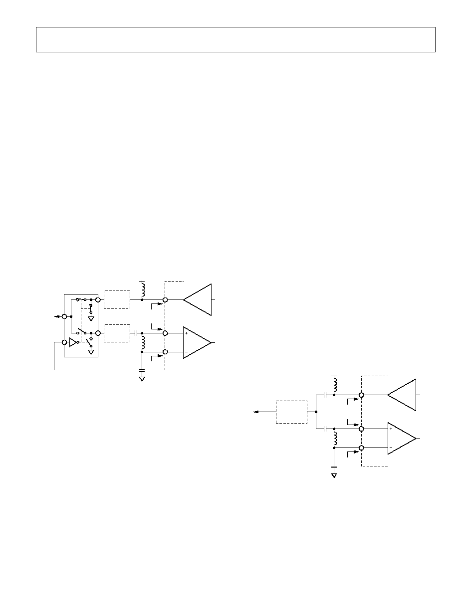
APPLICATIONS SECTION
LNA/PA MATCHING
The ADF7025 exhibits optimum performance in terms of
sensitivity, transmit power, and current consumption only if its
RF input and output ports are properly matched to the antenna
impedance. For cost-sensitive applications, the ADF7025 is
equipped with an internal Rx/Tx switch, which facilitates the
use of a simple combined passive PA/LNA matching network.
Alternatively, an external Rx/Tx switch, such as the Analog
Devices
ADG919
, can be used, which yields a slightly improved
receiver sensitivity and lower transmitter power consumption.
External Rx/Tx Switch
Figure 31 shows a configuration using an external Rx/Tx switch.
This configuration allows an independent optimization of the
matching and filter network in the transmit and receive path,
and is, therefore, more flexible and less difficult to design than
the configuration using the internal Rx/Tx switch. The PA is
biased through Inductor L1, while C1 blocks dc current. Both
elements, L1 and C1, also form the matching network, which
transforms the source impedance into the optimum PA load
impedance, Z
OPT
_PA.
PA
LNA
PA_OUT
RFIN
RFINB
V
BAT
L1
ADF7025
ADG919
OPTIONAL
BPF
(SAW)
OPTIONAL
LPF
L
A
C
A
C
B
Z
IN
_RFIN
Z
OPT
_PA
Z
IN
_RFIN
ANTENNA
Rx/Tx SELECT
05542-
031
Figure 31. ADF7025 with External Rx/Tx Switch
Z
OPT
_PA depends on various factors such as the required output
power, the frequency range, the supply voltage range, and the
temperature range. Selecting an appropriate Z
OPT
_PA helps to
minimize the Tx current consumption in the application. This
data sheet contains a number of Z
OPT
_PA values for representa-
tive conditions. Under certain conditions, however, it is
recommended to obtain a suitable Z
OPT
_PA value by means of a
load-pull measurement.
Due to the differential LNA input, the LNA matching network
must be designed to provide both a single-ended to differential
conversion and a complex conjugate impedance match. The
network with the lowest component count that can satisfy these
requirements is the configuration shown in Figure 31, which
consists of two capacitors and one inductor.
A first-order implementation of the matching network can be
obtained by understanding the arrangement as two L-type
matching networks in a back-to-back configuration. Due to the
asymmetry of the network with respect to ground, a compro-
mise between the input reflection coefficient and the maximum
differential signal swing at the LNA input must be established.
The use of appropriate CAD software is strongly recommended
for this optimization.
Depending on the antenna configuration, the user might need a
harmonic filter at the PA output to satisfy the spurious emission
requirement of the applicable government regulations. The
harmonic filter can be implemented in various ways, such as a
discrete LC filter or T-stage filter. Dielectric low-pass filter
components such as the LFL18924MTC1A052 (for operation in
the 915 MHz band), or LFL18869MTC2A160 (for operation in
the 868 MHz band), both by Murata Mfg. Co., Ltd., represent an
attractive alternative to discrete designs. The immunity of the
ADF7025 to strong out-of-band interference can be improved
by adding a band-pass filter in the Rx path.
Internal Rx/Tx Switch
Figure 32 shows the ADF7025 in a configuration where the
internal Rx/Tx switch is used with a combined LNA/PA
matching network. This is the configuration used in the
ADF7025DB1 Evaluation Board. For most applications, the
slight performance degradation of 1 dB to 2 dB caused by the
internal Rx/Tx switch is acceptable, allowing the user to take
advantage of the cost-saving potential of this solution. The
design of the combined matching network must compensate for
the reactance presented by the networks in the Tx and the Rx
paths, taking the state of the Rx/Tx switch into consideration.
PA
LNA
PA_OUT
RFIN
RFINB
V
BAT
L1
ADF7025
OPTIONAL
BPF OR LPF
L
A
C
A
C1
C
B
Z
IN
_RFIN
Z
OPT
_PA
Z
IN
_RFIN
ANTENNA
05
54
2-
0
3
2
Figure 32. ADF7025 with Internal Rx/Tx Switch
ADF7025
Rev. A | Page 24 of 44
The procedure typically requires several iterations until an
acceptable compromise is reached. The successful implementation
of a combined LNA/PA matching network for the ADF7025 is
critically dependent on the availability of an accurate electrical
model for the PC board. In this context, the use of a suitable CAD
package is strongly recommended. To avoid this effort, however, a
small form-factor reference design for the ADF7025 is provided,
including matching and harmonic filter components. The design
is on a 2-layer PCB to minimize cost. Gerber files are available
on the
www.analog.com
website.
TRANSMIT PROTOCOL AND CODING
CONSIDERATIONS
PREAMBLE
SYNC
WORD
ID
FIELD
DATA FIELD
CRC
05
54
2-
03
3
Figure 33. Typical Format of a Transmit Protocol
A dc-free preamble pattern is recommended for FSK
demodulation. The recommended preamble pattern is a dc-free
pattern such as a 10101010... pattern. Preamble patterns with
longer run-length constraints such as 11001100.... can also be
used. However, this results in a longer synchronization time of
the received bit stream in the receiver.
Manchester coding can be used for the entire transmit protocol.
However, the remaining fields that follow the preamble header
do not have to use dc-free coding. For these fields, the ADF7025
can accommodate coding schemes with a run-length of up to
six bits without any performance degradation.
If longer run-length coding must be supported, the ADF7025
has several other features that can be activated. These involve a
range of programmable options that allow the envelope detector
output to be frozen after preamble acquisition.
DEVICE PROGRAMMING AFTER INITIAL POWER-UP
Table 7 lists the minimum number of writes needed to set up
the ADF7025 in either Tx or Rx mode after CE is brought high.
Additional registers can also be written to tailor the part to a
particular application, such as setting up sync byte detection.
When going from Tx to Rx or vice versa, the user needs to write
only to the N register to alter the LO by 200 kHz and to toggle
the Tx/Rx bit.
Table 7. Minimum Register Writes Required for Tx/Rx Setup
Mode Registers
Tx 0
1
2
Rx
(FSK)
0 1 2 4 6 9
1
Tx to Rx and Rx to Tx
0
1
Register 9 should be programmed in receive mode in order to set the
recommended AGC threshold settings (low = 15, high = 79).
Figure 36 and Figure 37 show the recommended programming
sequence and associated timing for power-up from standby
mode.
INTERFACING TO MICROCONTROLLER/DSP
Low level device drivers are available for interfacing to the
ADF7025, the ADI ADuC84x microcontroller parts, or the
Blackfin® BF53x DSPs using the hardware connections shown in
Figure 34 and Figure 35.
MISO
ADuC84x
ADF7025
MOSI
SCLOCK
SS
P3.7
P3.2/INT0
P2.4
P2.5
TxRxDATA
RxCLK
CE
INT/LOCK
SREAD
SLE
P2.6
P2.7
SDATA
SCLK
GPIO
0
55
42
-
0
34
Figure 34. ADuC84X to ADF7025 Connection Diagram
MOSI
ADSP-BF533
ADF7025
MISO
PF5
RSCLK1
DT1PRI
DR1PRI
RFS1
PF6
SDATA
SLE
TxRxDATA
INT/LOCK
CE
VCC
GND
VCC
GND
SCK
SCLK
SREAD
TxRxCLK
0
5542-
035
Figure 35. BF533 to ADF7025 Connection Diagram
ADF7025
Rev. A | Page 25 of 44
2.0mA
3.65mA
14mA
A
D
F
7
0
2
5
I
D
D
TIME
REG.
READY
T
1
WR0
T
2
WR1
T
3
VCO
T
4
WR3
T
5
WR4
T
6
WR6
T
7
19mA TO
22mA
AGC/
RSSI
T
8
CDR
T
9
Rx
DATA
T
11
T
OFF
T
ON
XTAL
T
0
0
55
42
-
0
36
Figure 36. Rx Programming Sequence and Timing Diagram
Table 8. Power-Up Sequence Description
Parameter Value
Description/Notes
Signal to
Monitor
T
0
2 ms
XTAL starts power-up after CE is brought high. This typically depends on the XTAL
type and the load capacitance specified.
CLKOUT
T
1
10 µs
Time for regulator to power up. The serial interface can be written to after this time.
MUXOUT
T
2
, T
3
, T
5
,
T
6
, T
7
32 × 1/SPI_CLK
Time to write to a single register. Maximum SPI_CLK is 25 MHz.
T
4
1 ms
The VCO can power-up in parallel with the XTAL. This depends on the CVCO
capacitance value used. A value of 22 nF is recommended as a trade-off
between phase noise performance and power-up time.
CVCO pin
T
8
150 µs
This depends on the number of gain changes the AGC loop needs to cycle through
and AGC settings programmed. This is described in more detail in the AGC Information
section.
Analog RSSI
on TEST_A pin
T
9
5 × bit_period
This is the time for the clock and data recovery circuit to settle. This typically requires
5-bit transitions to acquire sync and is usually covered by the preamble.
T
11
Packet length
Number of bits in payload by the bit period.
ADF7025
Rev. A | Page 26 of 44
2.0mA
3.65mA
14mA
A
D
F
7
0
2
5
I
D
D
TIME
REG.
READY
T
1
WR0
T
2
WR1
T
3
XTAL + VCO
T
4
WR2
T
5
15mA TO
30mA
TxDATA
T
12
T
OFF
T
ON
05
54
2-
0
3
7
Figure 37. Tx Programming Sequence and Timing Diagram
ADF7025
Rev. A | Page 27 of 44
SERIAL INTERFACE
The serial interface allows the user to program the eleven 32-bit
registers using a 3-wire interface (SCLK, SDATA, and SLE). It
consists of a level shifter, a 32-bit shift register, and 11 latches.
Signals should be CMOS-compatible. The serial interface is
powered by the regulator, and, therefore, is inactive when CE
is low.
Data is clocked into the register, MSB first, on the rising edge of
each clock (SCLK). Data is transferred to one of 11 latches on
the rising edge of SLE. The destination latch is determined by
the value of the four control bits (C4 to C1). These are the
bottom four LSBs, DB3 to DB0, as shown in the timing diagram
in Figure 2. Data can also be read back on the SREAD pin.
READBACK FORMAT
The readback operation is initiated by writing a valid control
word to the readback register and setting the readback-enable
bit (R7_DB8 = 1). The readback can begin after the control
word has been latched with the SLE signal. SLE must be kept
high while the data is being read out. Each active edge at the
SCLK pin clocks the readback word out successively at the
SREAD pin, as shown in Figure 38, starting with the MSB first.
The data appearing at the first clock cycle following the latch
operation must be ignored.
RSSI Readback
The RSSI readback operation yields valid results in Rx mode.
The format of the readback word is shown in Figure 38. It
comprises the RSSI level information (Bit RV1 to Bit RV7), the
current filter gain (FG1 and FG2), and the current LNA gain
(LG1 and LG2) setting. The filter and LNA gain are coded in
accordance with the definitions in Register 9--AGC Register.
The input power can be calculated from the RSSI readback
value, as outlined in the RSSI/AGC section.
Battery Voltage ADCIN/Temperature Sensor Readback
The battery voltage is measured at Pin VDD4. The readback
information is contained in Bit RV1 to Bit RV7. This also
applies for the readback of the voltage at the ADCIN pin and
the temperature sensor. From the readback information, the
battery or ADCIN voltage can be determined using
V
BATTERY
= (Battery_Voltage_Readback)/21.1
V
ADCIN
= (ADCIN_Voltage_Readback)/42.1
Silicon Revision Readback
The silicon revision readback word is valid without setting any
other registers, especially directly after power-up. The silicon
revision word is coded with four quartets in BCD format. The
product code (PC) is coded with two quartets extending from
Bit RV9 to Bit RV16. The revision code (RV) is coded with one
quartet extending from Bit RV1 to Bit RV8. The product code
should read back as PC = 0x25. The current revision code
should read as RC = 0x08.
Filter Calibration Readback
The filter calibration readback word is contained in Bit RV1 to
Bit RV8 and is for diagnostic purposes only. Using the automatic
filter calibration function, accessible through Register 6, is
recommended. Before filter calibration is initiated, Decimal 32
should be read back.
READBACK MODE
DB15
X
X
RV16
0
RSSI READBACK
BATTERY VOLTAGE/ADCIN/
TEMP. SENSOR READBACK
SILICON REVISION
FILTER CAL READBACK
READBACK VALUE
DB14
X
X
RV15
0
DB13
X
X
RV14
0
DB12
X
X
RV13
0
DB11
X
X
RV12
0
DB10
LG2
X
RV11
0
DB9
LG1
X
RV10
0
DB8
FG2
X
RV9
0
DB7
FG1
X
RV8
RV8
DB6
RV7
RV7
RV7
RV7
DB5
RV6
RV6
RV6
RV6
DB4
RV5
RV5
RV5
RV5
DB3
RV4
RV4
RV4
RV4
DB2
RV3
RV3
RV3
RV3
DB1
RV2
RV2
RV2
RV2
DB0
RV1
RV1
RV1
RV1
05
54
2-
0
3
8
Figure 38. Readback Value Table
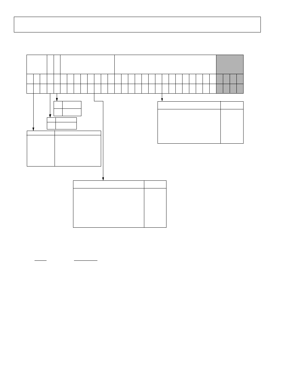
ADF7025
Rev. A | Page 28 of 44
REGISTERS
REGISTER 0--N REGISTER
TR1
TRANSMIT/
RECEIVE
0
TRANSMIT
RECEIVE
1
M3
M2
M1
MUXOUT
0
REGULATOR READY (DEFAULT)
0
R DIVIDER OUTPUT
0
N DIVIDER OUTPUT
0
DIGITAL LOCK DETECT
1
ANALOG LOCK DETECT
1
THREE-STATE
1
PLL TEST MODES
1
0
0
1
1
0
0
1
1
0
1
0
1
0
1
0
1
- TEST MODES
PLE1 PLL ENABLE
0
PLL OFF
1
PLL ON
N8
N7
N6
N5
N4
N3
N2
N1
N COUNTER
DIVIDE RATIO
0
31
0
32
.
.
.
1
253
1
254
1
0
0
.
.
.
1
1
1
0
1
.
.
.
.
.
.
1
1
1
1
0
1
1
1
.
.
.
1
0
1
1
1
.
.
.
1
0
1
1
1
.
.
.
1
0
0
1
1
.
.
.
.
.
.
1
0
1
0
1
255
15-BIT FRACTIONAL-N
8-BIT INTEGER-N
Tx
/
R
x
PLL
E
N
ABL
E
MUXOUT
ADDRESS
BITS
N5
N4
N8
M5
M6
M7
M8
M1
2
M1
3
M1
5
N1
N2
N3
M1
4
M9
M1
0
M1
1
M4
M3
TR
1
PL
E
1
M1
M3
M2
C2
(
0
)
C1
(
0
)
C3
(
0
)
C4
(
0
)
M1
M2
N7
N6
DB
1
6
DB
1
5
DB
1
4
DB
1
7
DB
2
0
DB
1
9
DB
1
8
DB
2
1
DB
1
3
DB
1
2
DB
1
1
DB
1
0
DB9
DB8
DB7
DB6
DB5
DB4
DB
2
2
DB
2
3
DB
2
4
DB
2
6
DB
2
7
DB
2
8
DB
2
5
DB1
DB0
DB2
DB3
DB
2
9
DB
3
0
DB
3
1
FRACTIONAL
DIVIDE RATIO
0
1
2
.
.
.
32764
32765
32766
32767
M15
0
0
0
.
.
.
1
1
1
1
M14
0
0
0
.
.
.
1
1
1
1
M13
0
0
0
.
.
.
1
1
1
1
...
...
...
...
...
...
...
...
...
...
...
M3
0
0
0
.
.
.
1
1
1
1
M2
0
0
1
.
.
.
0
0
1
1
M1
0
1
0
.
.
.
0
1
0
1
05
54
2-
0
3
9
Figure 39. Register 0--N Register
Register 0--N Register Comments
·
The Tx/Rx bit (R0_DB27) configures the part in Tx or Rx mode and also controls the state of the internal Tx/Rx switch.
·
)
2
(
15
N
Fractional
N
Integer
R
XTAL
F
OUT
+
×
=
·
If operating in 433 MHz band with the VCO band bit set, the desired frequency, F
OUT
, should be programmed to be twice the desired
operating frequency, due to removal of the divide-by-2 stage in feedback path.
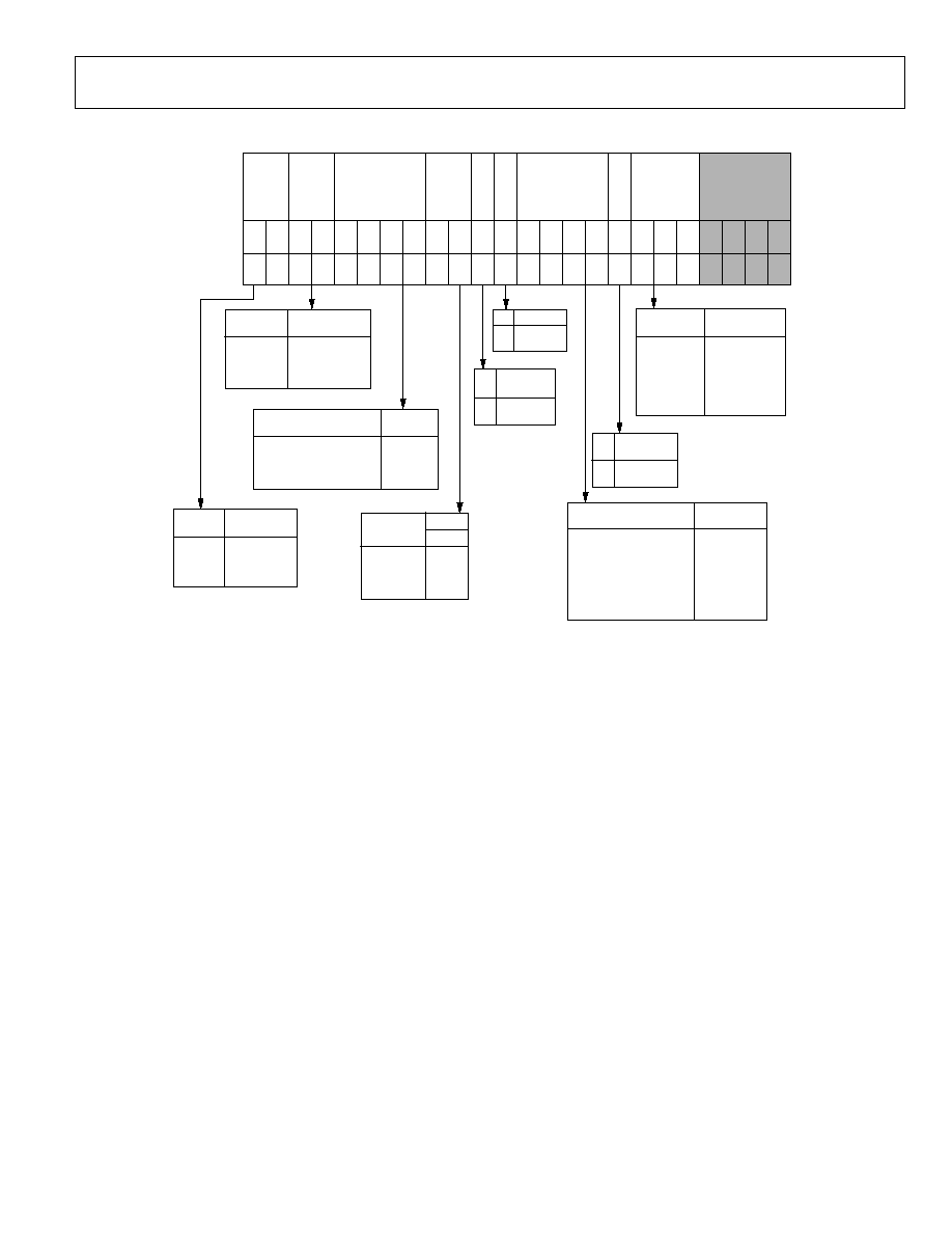
ADF7025
Rev. A | Page 29 of 44
REGISTER 1--OSCILLATOR/FILTER REGISTER
R3
R2
R1
RF R COUNTER
DIVIDE RATIO
0
0
.
.
.
1
1
2
.
.
.
7
1
0
.
.
.
1
0
1
.
.
.
1
X1 XTAL OSC
0
OFF
1
ON
VA2
VA1
FREQUENCY
OF OPERATION
0
850920
0
860930
1
870940
1
0
1
0
1
880950
D1
XTAL
DOUBLER
0
DISABLE
ENABLED
1
V1
VCO BAND
(MHz)
0
862956
1
431478
CP2
CP1
RSET
I
CP
(MA)
3.6k
0
0
0.3
0
1
0.9
1
0
1.5
1
1
2.1
VB4
VB3
VB2
VB1
VCO BIAS
CURRENT
0
0.25mA
0
0.5mA
.
1
1
0
.
1
0
1
.
1
0
0
.
1
4mA
IR2 IR1
FILTER
BANDWIDTH
0
600kHz
0
900kHz
1
1200kHz
1
0
1
0
1
NOT USED
CL4
CL3
CL2
CL1
CLK
OUT
DIVIDE RATIO
0
OFF
0
0
.
.
.
1
0
1
0
.
.
.
1
2
4
.
.
.
0
0
1
.
.
.
1
0
0
0
.
.
.
1
30
VCO BIAS
CP
CUR
RE
NT
V
C
O
BAND
XO
S
C
E
NABL
E
CLOCKOUT
DIVIDE
ADDRESS
BITS
R COUNTER
XT
A
L
DO
UBL
E
R
VC
O
ADJUS
T
IF FI
L
T
E
R
B
W
IR
2
IR
1
CL
1
CL
2
CL
3
CL
4
DD
2
VB
1
VB
3
VB
4
VA
1
VA
2
VB
2
X1
V1
DD
1
D1
R3
C2 (
0
)
C1 (
1
)
C3 (
0
)
C4 (
0
)
R1
R2
DB16
DB15
DB14
DB17
DB20
DB19
DB18
DB21
DB13
DB12
DB
1
1
DB10
DB
9
DB
8
DB
7
DB
6
DB
5
DB
4
DB22
DB23
DB
1
DB
0
DB
2
DB
3
05
54
2-
04
0
Figure 40. Register 1--Oscillator/Filter Register
Register 1--Oscillator/Filter Register Comments
·
The VCO Adjust Bits R1_DB[20:21] should be set to 0 for operation in the 862 MHz to 870 MHz band and set to 3 for operation in the
902 MHz to 928 MHz band.
·
VCO bias setting should be 0xA for operation in the 862 MHz to 870 MHz band and 0xC for operation in the 902 MHz to 928 MHz
band. All VCO gain numbers are specified for these settings.
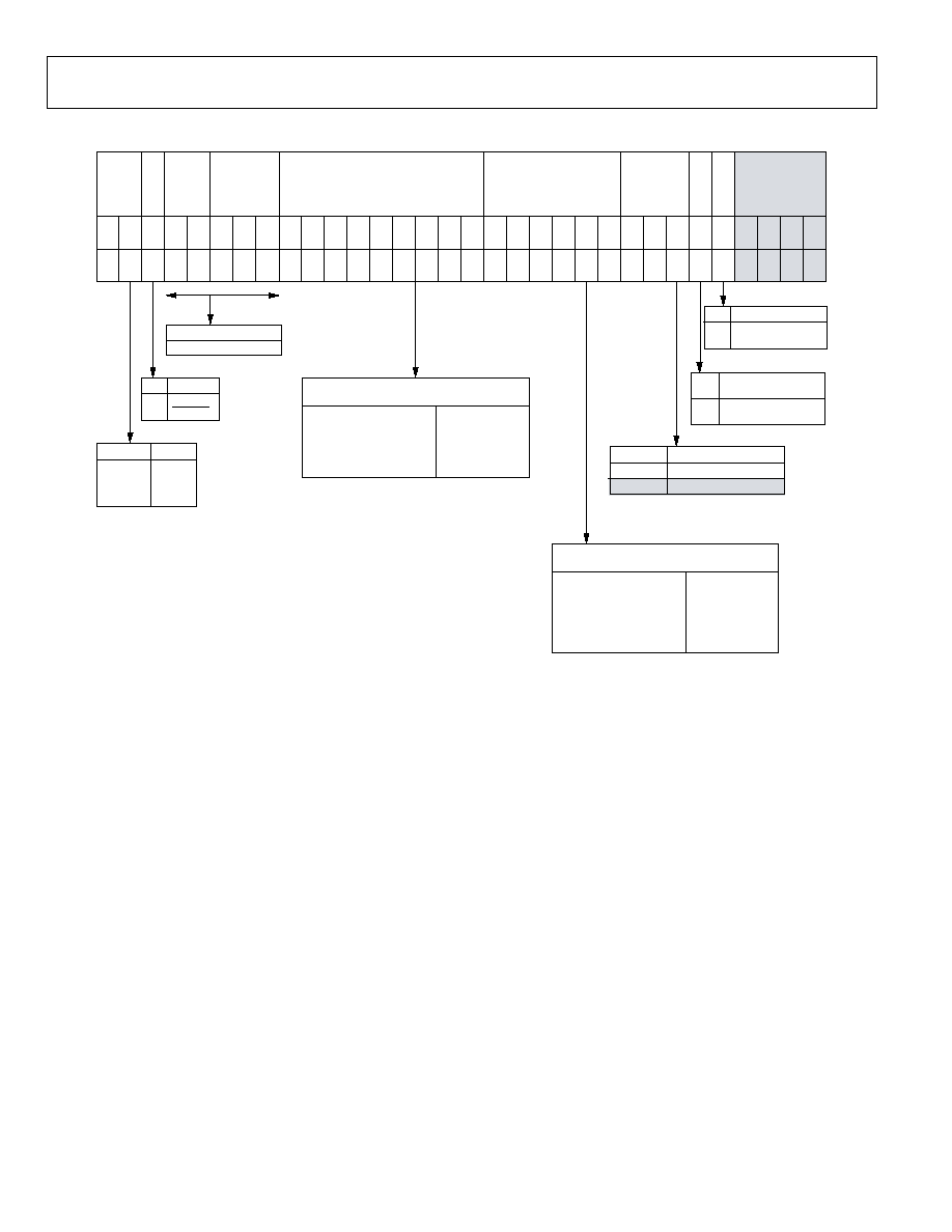
ADF7025
Rev. A | Page 30 of 44
REGISTER 2--TRANSMIT MODULATION REGISTER
MODULATION PARAMETER
POWER AMPLIFIER
GFSK MOD
CONTROL
I
NDE
X
CO
UN
T
E
R
Tx
DA
T
A
IN
V
E
R
T
PA BIAS
MODULATION
SCHEME
ADDRESS
BITS
PA
EN
A
B
L
E
MU
T
E
P
A
UNT
I
L
L
O
CK
D9
D8
MC
3
S3
P1
P2
P3
D1
D2
D4
D5
D6
D7
D3
P4
P5
P6
S2
S1
IC
1
IC
2
DI
1
PA
2
PA
1
C2 (
1
)
C1 (
0
)
C3 (
0
)
C4 (
0
)
PE
1
MP
1
MC
2
MC
1
DB16
DB15
DB14
DB17
DB20
DB19
DB18
DB21
DB13
DB12
DB
1
1
DB10
DB9
DB8
DB7
DB6
DB5
DB4
DB22
DB23
DB24
DB26
DB27
DB28
DB25
DB1
DB0
DB2
DB3
DB29
DB30
DB31
DI1
0
1
TxDATA
TxDATA
PA2
0
0
1
1
PA1
0
1
0
1
PA BIAS
5µA
7µA
9µA
11µA
IC2
X
IC1
X
MC3
X
MC2
X
MC1
X
D9
0
0
0
0
.
1
D3
0
0
0
0
.
1
....
....
....
....
....
....
....
D2
0
0
1
1
.
1
D1
0
1
0
1
.
1
FOR FSK MODE,
F DEVIATION
PLL MODE
1 × F
STEP
2 × F
STEP
3 × F
STEP
.
511 × F
STEP
P6
0
0
0
0
.
.
1
.
.
.
.
.
.
.
.
.
.
.
.
.
.
.
1
P2
X
0
0
1
.
.
1
P1
X
0
1
0
.
.
1
POWER AMPLIFIER OUTPUT LEVEL
PA OFF
16.0dBm
16 + 0.45dBm
16 + 0.90dBm
.
.
13dBm
PE1
0
1
POWER AMPLIFIER
OFF
ON
MP1
0
1
MUTE PA UNTIL
LOCK DETECT HIGH
OFF
ON
MODULATION SCHEME
FSK
INVALID
S2
0
X
S3
0
X
S1
0
X
05
54
2-
04
1
Figure 41. Register 2--Transmit Modulation Register
Register 2--Transmit Modulation Register Comments
·
F
STEP
= PFD/12
14
.
·
When operating in the 431 MHz to 464 MHz band, F
STEP
= PFD/12
15
.
·
PA bias default = 9 µA.
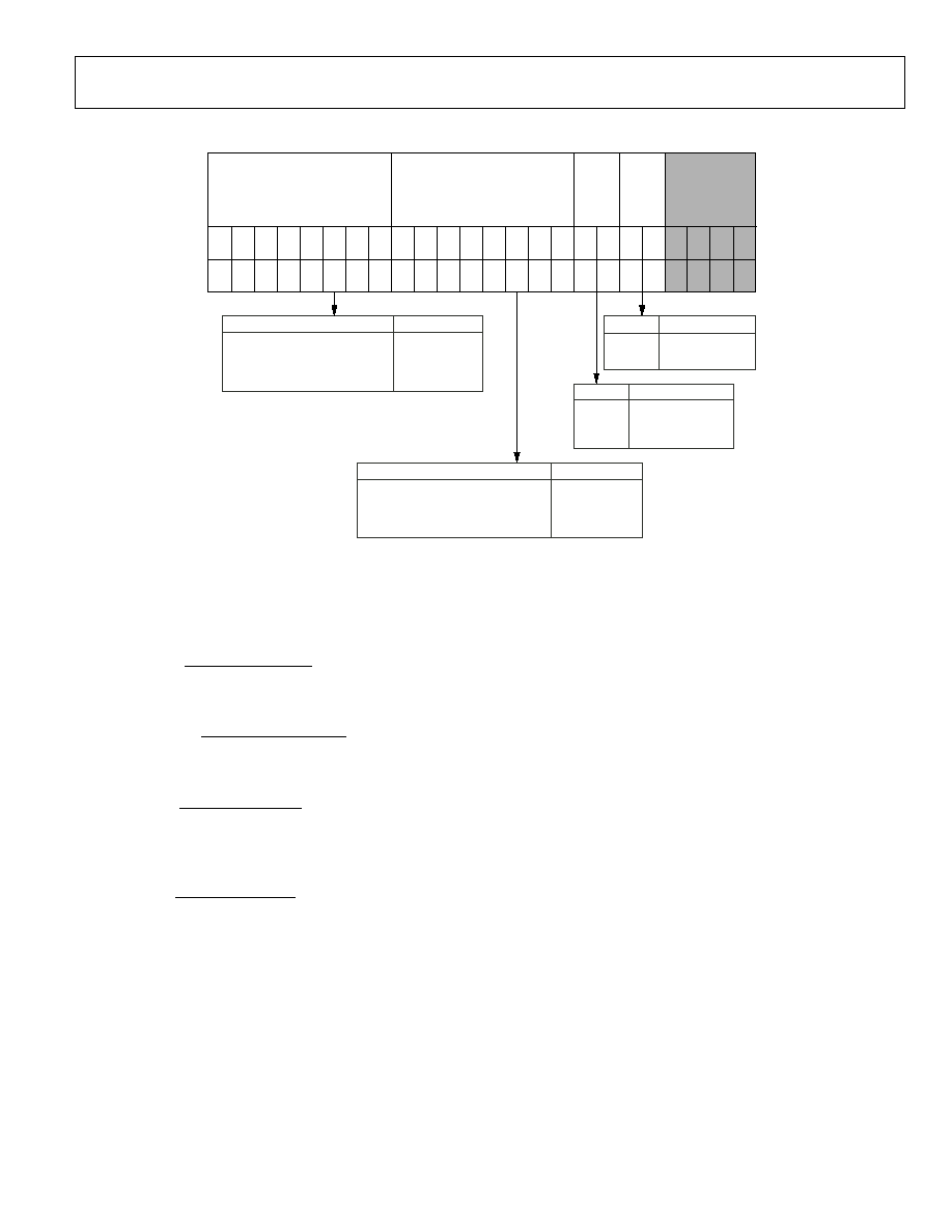
ADF7025
Rev. A | Page 31 of 44
REGISTER 3--RECEIVER CLOCK REGISTER
FS8
0
0
.
1
1
FS7
0
0
.
1
1
FS3
0
0
.
1
1
...
...
...
...
...
...
FS2
0
1
.
1
1
FS1
1
0
.
0
1
CDR_CLK_DIVIDE
1
2
.
254
255
BK2
0
0
1
BK1
0
1
x
BBOS_CLK_DIVIDE
4
8
16
SK8
0
0
.
1
1
SK7
0
0
.
1
1
SK3
0
0
.
1
1
...
...
...
...
...
...
SK2
0
1
.
1
1
SK1
1
0
.
0
1
SEQ_CLK_DIVIDE
1
2
.
254
255
OK2
0
0
1
1
OK1
0
1
0
1
DEMOD_CLK_DIVIDE
4
1
2
3
SEQUENCER CLOCK DIVIDE
CDR CLOCK DIVIDE
BB
O
F
F
S
E
T
C
L
O
CK DI
V
I
D
E
DE
M
O
D
C
L
O
CK DI
V
I
D
E
ADDRESS
BITS
SK
8
SK
7
FS
1
FS
2
FS
3
FS
4
FS
8
SK
1
SK
3
SK
4
SK
5
SK
6
SK
2
FS
5
FS
6
FS
7
OK
2
OK
1
C2
(
1
)
C1
(
1
)
C3
(
0
)
C4
(
0
)
BK
1
BK
2
DB
1
6
DB
1
5
DB
1
4
DB
1
7
DB
2
0
DB
1
9
DB
1
8
DB
2
1
DB
1
3
DB
1
2
DB
1
1
DB
1
0
DB
9
DB
8
DB
7
DB
6
DB
5
DB
4
DB
2
2
DB
2
3
DB
1
DB
0
DB
2
DB
3
05
542
-
0
4
2
Figure 42. Register 3--Receiver Clock Register
Register 3--Receiver Clock Register Comments
·
Baseband offset clock frequency (BBOS_CLK) must be greater than 1 MHz and less than 2 MHz, where:
DIVIDE
CLK
BBOS
XTAL
CLK
BBOS
_
_
_
=
·
The demodulator clock (DEMOD_CLK) must be < 12 MHz, where:
DIVIDE
CLK
DEMOD
XTAL
CLK
DEMOD
_
_
_
=
·
Data/clock recovery frequency (CDR_CLK) should be within 2% of (32 × data rate), where:
DIVIDE
CLK
CDR
CLK
DEMOD
CLK
CDR
_
_
_
_
=
Note that this can affect the choice of XTAL, depending on the desired data rate.
·
The sequencer clock (SEQ_CLK) supplies the clock to the digital receive block. It should be close to 100 kHz.
DIVIDE
CLK
SEQ
XTAL
CLK
SEQ
_
_
_
=
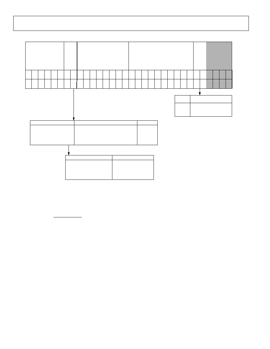
ADF7025
Rev. A | Page 32 of 44
REGISTER 4--DEMODULATOR SETUP REGISTER
DEMODULATOR LOCK SETTING
POSTDEMODULATOR BW
DE
M
O
D
SE
L
E
C
T
DE
M
O
D L
O
CK/
S
Y
NC W
O
RD
M
A
T
C
H
ADDRESS
BITS
DL
8
DL
7
DW
3
DW
4
DW
5
DW
6
DW
10
DL
1
DL
3
DL
4
DL
5
DL
6
DL
2
DW
7
DW
8
DW
9
DW
2
DW
1
C2(
0
)
C1(
0
)
C3(
1
)
C4(
0
)
DS
1
DS
2
LM2
LM1
DB16
DB15
DB14
DB17
DB20
DB19
DB18
DB21
DB13
DB12
DB
1
1
DB10
DB9
DB8
DB7
DB6
DB5
DB4
DB22
DB23
DB24
DB26
DB27
DB28
DB25
DB1
DB0
DB2
DB3
DB29
DB30
DB31
DS2
0
0
1
1
DS1
0
1
0
1
DEMODULATOR
TYPE
LINEAR DEMODULATOR
CORRELATOR/DEMODULATOR
INVALID
INVALID
LM2
0
0
0
0
1
1
DEMOD MODE
0
1
2
3
4
5
LM1
0
0
1
1
0
1
DEMOD LOCK/SYNC WORD MATCH
SERIAL PORT CONTROL FREE RUNNING
SERIAL PORT CONTROL LOCK THRESHOLD
SYNC WORD DETECT FREE RUNNING
SYNC WORD DETECT LOCK THRESHOLD
INTERRUPT/LOCK PIN LOCKS THRESHOLD
DEMOD LOCKED AFTER DL8DL1 BITS
INT/LOCK PIN
OUTPUT
OUTPUT
INPUT
DL8
0
1
0
1
X
DL8
DL7
0
0
0
.
1
1
DL8
0
0
0
.
1
1
DL3
0
0
0
.
1
1
...
...
...
...
...
...
...
DL2
0
0
1
.
1
1
DL1
0
1
0
.
0
1
LOCK_THRESHOLD_TIMEOUT
0
1
2
.
254
255
MODE5 ONLY
05
54
2-
04
3
Figure 43. Register 4--Demodulator Setup Register
Register 4--Demodulator Setup Register Comments
·
Demodulator Mode 1, Demodulator Mode 3, Demodulator Mode 4, and Demodulator Mode 5 are modes that can be activated to allow
the ADF7025 to demodulate data-encoding schemes that have run-length constraints greater than 7.
·
Post_Demod_BW =
DEMOD_CLK
F
2
CUTOFF
11
×
×
, where the cutoff frequency (F
CUTOFF
) of the postdemodulator filter should typically be 0.75 times
the data rate.
·
For Mode 5, the Timeout Delay to Lock Threshold = (LOCK_THRESHOLD_SETTING)/SEQ_CLK, where SEQ_CLK is defined in the
Register 3--Receiver Clock Register section.
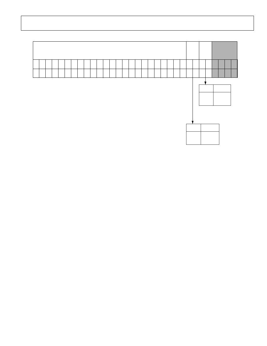
ADF7025
Rev. A | Page 33 of 44
REGISTER 5--SYNC BYTE REGISTER
PL2
0
0
1
1
PL1
0
1
0
1
SYNC BYTE
LENGTH
12 BITS
16 BITS
20 BITS
24 BITS
MT2
0
0
1
1
MT1
0
1
0
1
MATCHING
TOLERANCE
0 ERRORS
1 ERROR
2 ERRORS
3 ERRORS
SYNC BYTE SEQUENCE
CONTROL
BITS
S
Y
NC BY
T
E
LE
N
G
TH
M
A
T
C
HI
NG
T
O
L
E
RANCE
MT
2
MT
1
C2(
0
)
C1(
1
)
C3(
1
)
C4(
0
)
PL
1
PL
2
DB16
DB15
DB14
DB17
DB20
DB19
DB18
DB21
DB13
DB12
DB
1
1
DB10
DB
9
DB
8
DB
7
DB
6
DB
5
DB
4
DB22
DB23
DB24
DB26
DB27
DB28
DB25
DB
1
DB
0
DB
2
DB
3
DB29
DB30
DB31
05
54
2-
04
4
Figure 44. Register 5--Sync Byte Register
Register 5--Sync Byte Register Comments
·
Sync byte detect is enabled by programming Bits R4_DB [25:23] to 010 or 011.
·
This register allows a 24-bit sync byte sequence to be stored internally. If the sync byte detect mode is selected, then the INT/LOCK pin
goes high when the sync byte has been detected in Rx mode. Once the sync word detect signal has gone high, it goes low again after
nine data bits.
·
The transmitter must transmit the MSB of the sync byte first and the LSB last to ensure proper alignment in the receiver sync byte
detection hardware.
·
Choose a sync byte pattern that has good autocorrelation properties.
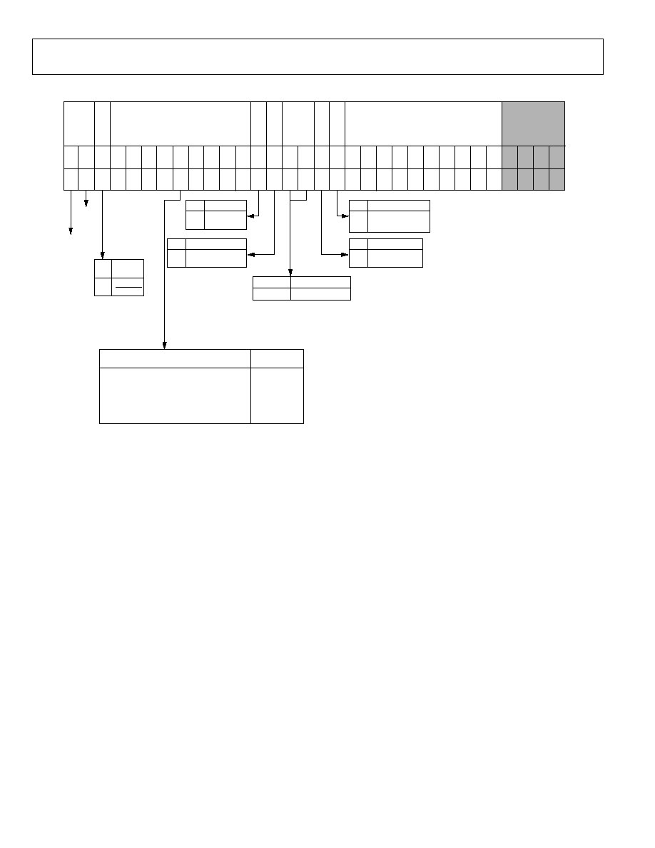
ADF7025
Rev. A | Page 34 of 44
REGISTER 6--CORRELATOR/DEMODULATOR REGISTER
DEMOD
RESET
CDR
RESET
DISCRIMINATOR BW
IF FILTER DIVIDER
LN
A
C
URRE
N
T
LN
A
M
O
D
E
DO
T
P
R
O
DUCT
Rx
D
A
T
A
IN
V
E
R
T
IF
FI
L
T
E
R
CA
L
MI
X
E
R
L
I
NE
ARI
T
Y
Rx
RESET
ADDRESS
BITS
FC
4
FC
3
FC
7
TD
5
TD
6
TD
7
TD
8
LG
1
LI
1
ML
1
CA1
FC
1
FC
2
LI
2
TD
9
TD
1
0
DP
1
TD
4
TD
3
FC
8
FC
9
RI
1
C2(
1
)
C1(
0
)
C3(
1
)
C4(
0
)
TD
1
TD
2
FC
6
FC
5
DB
1
6
DB
1
5
DB
1
4
DB
1
7
DB
2
0
DB
1
9
DB
1
8
DB
2
1
DB
1
3
DB
1
2
DB
1
1
DB
1
0
DB9
DB8
DB7
DB6
DB5
DB4
DB
2
2
DB
2
3
DB
2
4
DB
2
6
DB
2
7
DB
2
8
DB
2
5
DB1
DB0
DB2
DB3
DB
2
9
DB
3
0
DB
3
1
RI1
0
1
RxDATA
INVERT
RxDATA
RxDATA
CA1
0
1
FILTER CAL
NO CAL
CALIBRATE
ML1
0
1
MIXER LINEARITY
DEFAULT
HIGH
DP1
0
1
DOT PRODUCT
CROSS PRODUCT
INVALID
LG1
0
1
LNA MODE
DEFAULT
REDUCED GAIN
FC3
0
0
.
.
.
.
1
FC1
1
0
.
.
.
.
1
FILTER CLOCK
DIVIDE RATIO
1
2
.
.
.
.
511
FC2
0
1
.
.
.
.
1
FC9
0
0
.
.
.
.
1
FC6
0
0
.
.
.
.
1
.
.
.
.
.
.
.
.
FC5
0
0
.
.
.
.
1
FC4
0
0
.
.
.
.
1
LI2
0
LI1
0
LNA BIAS
800µA (DEFAULT)
05
54
2-
0
4
5
Figure 45. Register 6--Correlator/Demodulator Register
Register 6--Correlator/Demodulator Register Comments
·
See the FSK Correlator/Demodulator section for an example of how to determine register settings.
·
Nonadherence to correlator programming guidelines results in poor sensitivity.
·
The filter clock is used to calibrate the LP filter. The filter clock divide ratio should be adjusted so that the frequency is 50 kHz.
The formula is XTAL/FILTER_CLOCK_DIVIDE.
·
The filter should be calibrated only when the crystal oscillator is settled. The filter calibration is initiated every time Bit R6_DB19
is set high.
·
Discriminator_BW = DEMOD_CLK/(4 × DEVIATION_Frequency). See the FSK Correlator/Demodulator section.
Maximum value = 600.
·
When LNA Mode = 1 (reduced gain mode), the Rx is prevented from selecting the highest LNA gain setting. This can be used when
linearity is a concern. See the Readback Format section for details of the different Rx modes.
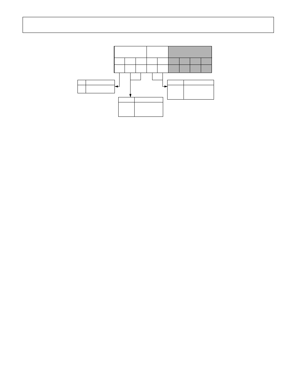
ADF7025
Rev. A | Page 35 of 44
REGISTER 7--READBACK SETUP REGISTER
AD1
AD2
RB1
RB2
RB3
DB8
DB7
DB6
DB5
DB4
DB3
DB2
C2(1)
C1(1)
CONTROL
BITS
DB1
DB0
C3(1)
C4(0)
READBACK
SELECT
ADC
MODE
AD2
0
0
1
1
AD1
0
1
0
1
ADC MODE
MEASURE RSSI
BATTERY VOLTAGE
TEMP SENSOR
TO EXTERNAL PIN
RB2
0
0
1
1
RB1
0
1
0
1
READBACK MODE
INVALID
ADC OUTPUT
FILTER CAL
SILICON REV
RB3
0
1
READBACK
DISABLED
ENABLED
05
54
2-
0
4
6
Figure 46. Register 7--Readback Setup Register
Register 7--Readback Setup Register Comments
·
Readback of the measured RSSI value is valid only in Rx mode. Readback of the battery voltage, the temperature sensor, and the voltage
at the external pin is not available in Rx mode if AGC is enabled.
·
Readback of the ADC value is valid in Tx mode only if the log amp/RSSI has not been disabled through the Power-Down Bit R8_DB10.
The log amp/RSSI section is active by default upon enabling Tx mode.
·
See the Readback Format section for more information.
ADF7025
Rev. A | Page 36 of 44
REGISTER 8--POWER-DOWN TEST REGISTER
PD1
PD2
PD3
PD4
PD5
DB8
DB7
DB6
DB5
DB4
DB3
DB2
C2(0)
C1(0)
CONTROL
BITS
DB1
DB0
C3(0)
C4(1)
LOG AMP/
RSSI
SYN
T
H
E
NAB
L
E
VC
O
E
NAB
L
E
L
NA/
M
I
X
E
R
E
NAB
L
E
FI
L
T
E
R
E
NAB
L
E
ADC
E
NAB
L
E
DE
M
O
D
E
NAB
L
E
I
N
T
E
RNA
L T
x
/
R
x
SW
I
T
C
H
EN
A
B
L
E
P
A
E
NAB
L
E
Rx M
O
D
E
PD7
DB15
DB14
DB13
DB12
DB11
LR1
PD6
DB10
DB9
LR2
SW1
PD7
0
1
PA (Rx MODE)
PA OFF
PA ON
SW1
0
1
Tx/Rx SWITCH
DEFAULT (ON)
OFF
PD6
0
1
DEMOD ENABLE
DEMOD OFF
DEMOD ON
PD5
0
1
ADC ENABLE
ADC OFF
ADC ON
LR2
X
X
LR1
0
1
RSSI MODE
RSSI OFF
RSSI ON
PD4
0
1
FILTER ENABLE
FILTER OFF
FILTER ON
PD3
0
1
LNA/MIXER ENABLE
LNA/MIXER OFF
LNA/MIXER ON
PLE1
(FROM REG 0)
0
0
0
0
1
PD2
0
0
1
1
X
LOOP
CONDITION
VCO/PLL OFF
PLL ON
VCO ON
PLL/VCO ON
PLL/VCO ON
PD1
0
1
0
1
X
0
55
42
-
0
4
7
Figure 47. Register 8--Power-Down Test Register
Register 8--Power-Down Test Register Comments
·
For a combined LNA/PA matching network, Bit R8_DB12 should always be set to 0. This is the power-up default condition.
·
It is not necessary to write to this register under normal operating conditions.
ADF7025
Rev. A | Page 37 of 44
REGISTER 9--AGC REGISTER
AGC HIGH THRESHOLD
LNA
GAIN
FILTER
GAIN
DIGITAL
TEST IQ
AG
C
S
E
ARCH
GA
IN
CO
NT
RO
L
FI
L
T
E
R
CU
RRE
NT
AGC LOW THRESHOLD
ADDRESS
BITS
FG2
FG1
GL5
GL6
GL7
GH
1
GH
5
GH
6
GS
1
GC
1
LG1
LG2
GH
7
GH
2
GH
3
GH
4
GL4
GL3
C2(
0
)
C1(
1
)
C3(
0
)
C4(
1
)
GL1
GL2
FI1
DB16
DB15
DB14
DB17
DB20
DB19
DB18
DB21
DB13
DB12
DB
1
1
DB10
DB
9
DB
8
DB
7
DB
6
DB
5
DB
4
DB22
DB23
DB24
DB26
DB27
DB28
DB25
DB
1
DB
0
DB
2
DB
3
DB29
DB30
DB31
FI1
0
1
FILTER CURRENT
LOW
HIGH
GS1
0
1
AGC SEARCH
AUTO AGC
HOLD SETTING
GC1
0
1
GAIN CONTROL
AUTO
USER
FG2
0
0
1
1
FG1
0
1
0
1
FILTER GAIN
8
24
72
INVALID
LG2
0
0
1
1
LG1
0
1
0
1
LNA GAIN
<1
3
10
30
GL3
0
0
0
1
.
.
.
1
1
1
GL1
1
0
1
0
.
.
.
1
0
1
AGC LOW
THRESHOLD
1
2
3
4
.
.
.
61
62
63
GL2
0
1
1
0
.
.
.
0
1
1
GL7
0
0
0
0
.
.
.
1
1
1
GL6
0
0
0
0
.
.
.
1
1
1
GL5
0
0
0
0
.
.
.
1
1
1
GL4
0
0
0
0
.
.
.
1
1
1
GH3
0
0
0
1
.
.
.
1
1
0
GH1
1
0
1
0
.
.
.
0
1
0
RSSI LEVEL
CODE
1
2
3
4
.
.
.
78
79
80
GH2
0
1
1
0
.
.
.
1
1
0
GH7
0
0
0
0
.
.
.
1
1
1
GH6
0
0
0
0
.
.
.
0
0
0
GH5
0
0
0
0
.
.
.
0
0
1
GH4
0
0
0
0
.
.
.
1
1
0
05
54
2
-
04
8
Figure 48. Register 9--AGC Register
Register 9--AGC Register Comments
·
The recommended AGC threshold settings are AGC_LOW_THRESHOLD = 15, AGC_HIGH_THRESHOLD = 79.
The default settings (that is, if this register is not programmed) are AGC_LOW_THRESHOLD = 30,
default AGC_HIGH_THRESHOLD = 70. See the RSSI/AGC section for details.
·
AGC high and low settings must be more than 30 apart to ensure correct operation.
·
LNA gain of 30 is available only if LNA mode, R6_DB15, is set to 0.
ADF7025
Rev. A | Page 38 of 44
REGISTER 10--AGC 2 REGISTER
AGC DELAY
I/Q GAIN ADJUST
LEAK FACTOR
I/Q PHASE
ADJUST
UP
/
D
O
W
N
RE
S
E
RV
E
D
SE
L
E
C
T
I/
Q
SE
L
E
C
T
I/
Q
PEAK RESPONSE
ADDRESS
BITS
R1
SI
Q
1
PH
3
GL4
GL5
GL6
GL7
DH4
GC
1
GC
3
GC
4
GC
5
UD1
GC
2
DH1
DH2
DH3
PR
4
PR
3
PH
4
SI
Q
2
C2(
1
)
C1(
0
)
C3(
0
)
C4(
1
)
PR
1
PR
2
PH
2
PH
1
DB16
DB15
DB14
DB17
DB20
DB19
DB18
DB21
DB13
DB12
DB
1
1
DB10
DB
9
DB
8
DB
7
DB
6
DB
5
DB
4
DB22
DB23
DB24
DB26
DB27
DB28
DB25
DB
1
DB
0
DB
2
DB
3
DB29
DB30
DB31
SIQ2
0
1
SELECT IQ
PHASE TO I CHANNEL
PHASE TO Q CHANNEL
SIQ2
0
1
SELECT IQ
GAIN TO I CHANNEL
GAIN TO Q CHANNEL
DEFAULT = 0xA
DEFAULT = 0x2
DEFAULT = 0xA
05
54
2-
04
9
Figure 49. Register 10--AGC 2 Register
Register 10--AGC 2 Register Comments
·
Register 10 is not used under normal operating conditions.
·
If adjusting AGC Delay or Leak Factor, clear Bit DB31 to Bit DB16.
ADF7025
Rev. A | Page 39 of 44
REGISTER 12--TEST REGISTER
CO
UNT
E
R
R
E
SET
DIGITAL
TEST MODES
-
TEST MODES
ANALOG TEST
MUX
IMAGE FILTER ADJUST
OS
C
T
E
S
T
F
O
RCE
LD
H
I
G
H
S
O
U
RCE
PR
ES
C
A
L
E
R
PLL TEST MODES
ADDRESS
BITS
SF
6
SF
5
T5
T6
T7
T8
SF
1
SF
2
SF
3
SF
4
T9
T4
T3
PR
E
C2(
0
)
C1(
0
)
C3(
1
)
C4(
1
)
T1
T2
QT
1
CS
1
DB16
DB15
DB14
DB17
DB20
DB19
DB18
DB21
DB13
DB12
DB
1
1
DB10
DB9
DB8
DB7
DB6
DB5
DB4
DB22
DB23
DB24
DB26
DB27
DB28
DB25
DB1
DB0
DB2
DB3
DB29
DB30
DB31
P
0
1
PRESCALER
4/5 (DEFAULT)
8/9
CR1
0
1
COUNTER RESET
DEFAULT
RESET
CS1
0
1
CAL SOURCE
INTERNAL
SERIAL IF BW CAL
DEFAULT = 32. INCREASE
NUMBER TO INCREASE BW
IF USER CAL ON
0
55
42
-
0
50
Figure 50. Register 12--Test Register
Using the Test DAC on the ADF7025 to Implement
Analog FM DEMOD and Measuring SNR
The test DAC allows the output of the postdemodulator filter
for both the linear and correlator/demodulators to be viewed
externally. It takes the 16-bit filter output and converts it to a
high frequency, single-bit output using a second-order error
feedback - converter. The output can be viewed on the
XCLK
OUT
pin. This signal, when IF-filtered appropriately, can
then be used to
·
Monitor the signals at the FSK postdemodulator filter
output. This allows the demodulator output SNR to be
measured. Eye diagrams can also be constructed of the
received bit stream to measure the received signal quality.
·
Provide analog FM demodulation.
While the correlators and filters are clocked by DEMOD_CLK,
CDR_CLK clocks the test DAC. Note that, although the test
DAC functions in a regular user mode, the best performance is
achieved when the CDR_CLK is increased up to or above the
frequency of DEMOD_CLK. The CDR block does not function
when this condition exists.
Programming the test register, Register 12, enables the test
DAC. Both the linear and correlator/demodulator outputs
can be multiplexed into the DAC.
Register 13 allows a fixed offset term to be removed from the
signal in the case where there is an error in the received signal
frequency. If there is a frequency error in the signal, the user
should program half this value into the offset removal field.
It also has a signal gain term to allow usage of the maximum
dynamic range of the DAC.
Setting Up the Test DAC
·
Digital test modes = 7: enables the test DAC, with no
offset removal (0x0001C00C).
·
Digital test modes = 10: enables the test DAC, with
offset removal.
The output of the active demodulator drives the DAC; that is, if
the FSK correlator/demodulator is selected, the correlator filter
output drives the DAC.
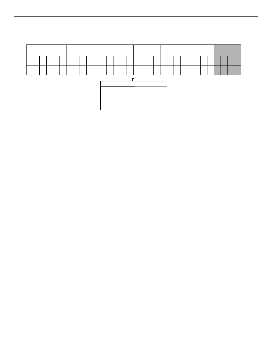
ADF7025
Rev. A | Page 40 of 44
REGISTER 13--OFFSET REMOVAL AND SIGNAL GAIN REGISTER
KP
KI
CONTROL
BITS
PULSE
EXTENSION
TEST DAC GAIN
TEST DAC OFFSET REMOVAL
PE1
PE2
PE3
PE4
C2(
0
)
C1(
1
)
C3(
1
)
C4(
1
)
DB16
DB15
DB14
DB17
DB20
DB19
DB18
DB21
DB13
DB12
DB
1
1
DB10
DB9
DB8
DB7
DB6
DB5
DB4
DB22
DB23
DB24
DB26
DB27
DB28
DB25
DB1
DB0
DB2
DB3
DB29
DB30
DB31
PE4
0
0
0
.
.
.
1
PE3
0
0
0
.
.
.
1
PE2
0
0
1
.
.
.
1
PULSE EXTENSION
NORMAL PULSE WIDTH
2× PULSE WIDTH
3× PULSE WIDTH
.
.
.
16× PULSE WIDTH
PE1
0
1
0
.
.
.
1
05
54
2-
0
5
1
Figure 51. Register 13--Offset Removal and Signal Gain Register
Register 13--Offset Removal and Signal Gain Register Comments
Because the linear demodulator output is proportional to frequency, it usually consists of an offset combined with a relatively
low signal. The offset can be removed, up to a maximum of 1.0, and gained to use the full dynamic range of the DAC, as follows:
DAC_Input = (2^ Test_DAC_Gain) × (Signal - Test_DAC_Offset_Removal/4096).
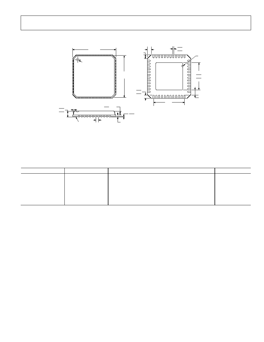
ADF7025
Rev. A | Page 41 of 44
OUTLINE DIMENSIONS
PIN 1
INDICATOR
TOP
VIEW
6.75
BSC SQ
7.00
BSC SQ
1
48
12
13
37
36
24
25
4.25
4.10 SQ
3.95
0.50
0.40
0.30
0.30
0.23
0.18
0.50 BSC
12° MAX
0.20 REF
0.80 MAX
0.65 TYP
1.00
0.85
0.80
5.50
REF
0.05 MAX
0.02 NOM
0.60 MAX
0.60 MAX
PIN 1
INDICATOR
COPLANARITY
0.08
SEATING
PLANE
0.25 MIN
EXPOSED
PAD
(BOTTOM VIEW)
COMPLIANT TO JEDEC STANDARDS MO-220-VKKD-2
Figure 52. 48-Lead Lead Frame Chip Scale Package [LFCSP_VQ]
7 mm × 7 mm Body, Very Thin Quad
(CP-48-3)
Dimensions shown in millimeters
ORDERING GUIDE
Model
Temperature Range
Package Description
Package Option
ADF7025BCPZ
1
-40°C to +85°C
48-Lead Lead Frame Chip Scale Package [LFCSP_VQ]
CP-48-3
ADF7025BCPZ-RL
1
-40°C to +85°C
48-Lead Lead Frame Chip Scale Package [LFCSP_VQ]
CP-48-3
ADF7025BCPZ-RL7
1
-40°C to +85°C
48-Lead Lead Frame Chip Scale Package [LFCSP_VQ]
CP-48-3
EVAL-ADF70XXMB
Control
Mother
Board
EVAL-ADF70XXMB2
Evaluation
Platform
EVAL-ADF7025DB1
902928 MHz Daughter Board
1
Z = Pb-free part.

ADF7025
Rev. A | Page 42 of 44
NOTES

ADF7025
Rev. A | Page 43 of 44
NOTES

ADF7025
Rev. A | Page 44 of 44
NOTES
©2006 Analog Devices, Inc. All rights reserved. Trademarks and
registered trademarks are the property of their respective owners.
D05542-0-2/06(A)
Document Outline