Document Outline
- FEATURES
- GENERAL DESCRIPTION
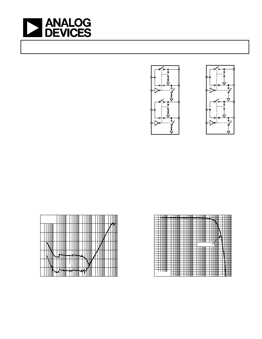
- FUNCTIONAL BLOCK DIAGRAMS
- PRODUCT HIGHLIGHTS
- ˛ˇ
- ˛ˇ
- ˛ˇ
- ˛ˇ
- ˛ˇ
- ˛ˇ
- ˛ˇ
- ˛ˇ
- ˛ˇ
Wideband 4 GHz, 36 dB Isolation at 1 GHz,
CMOS 1.65 V to 2.75 V, Dual SPDT
ADG936/ADG936-R
Rev. 0
Information furnished by Analog Devices is believed to be accurate and reliable.
However, no responsibility is assumed by Analog Devices for its use, nor for any
infringements of patents or other rights of third parties that may result from its use.
Specifications subject to change without notice. No license is granted by implication
or otherwise under any patent or patent rights of Analog Devices. Trademarks and
registered trademarks are the property of their respective owners.
One Technology Way, P.O. Box 9106, Norwood, MA 02062-9106, U.S.A.
Tel: 781.329.4700
www.analog.com
Fax: 781.326.8703
© 2004 Analog Devices, Inc. All rights reserved.
FEATURES
Wideband switch: -3 dB @ 4 GHz
ADG936 absorptive dual SPDT
ADG936-R reflective dual SPDT
High off isolation (36 dB @ 1 GHz)
Low insertion loss (0.9 dB dc to 1 GHz)
Single 1.65 to 2.75 V power supply
CMOS/LVTTL control logic
20-lead TSSOP and 4 mm ◊ 4 mm LFCSP package
Low power consumption (1 µA max)
APPLICATIONS
Wireless communications
General-purpose RF switching
Dual-band applications
High speed filter selection
Digital transceiver front end switch
IF switching
Tuner modules
Antenna diversity switching
FUNCTIONAL BLOCK DIAGRAMS
INB
RF1B
RF2B
04503-0-001
RFCB
ADG936
INA
RF1A
RF2A
RFCA
50
50
50
50
INA
INB
RF1A
RF2A
RF1B
RF2B
04503-0-012
RFCB
RFCA
ADG936-R
Figure 1.
Figure 2.
GENERAL DESCRIPTION
The ADG936/ADG936-R are wideband analog switches that
comprise two independently selectable SPDT switches using a
CMOS process to provide high isolation and low insertion loss
to 1 GHz. The ADG936 is an absorptive/matched dual SPDT
with 50 terminated shunt legs; the ADG936-R is a reflective
dual SPDT. These devices are designed such that the isolation is
high over the dc to 1 GHz frequency range. They have on-board
CMOS control logic, eliminating the need for external
controlling circuitry. The control inputs are both CMOS and
LVTTL compatible. The low power consumption of these
CMOS devices makes them ideally suited for wireless
applications and general-purpose high frequency switching.
PRODUCT HIGHLIGHTS
1.
≠36 dB off isolation @ 1 GHz.
2.
0.9 dB insertion loss @ 1 GHz.
3.
20-lead TSSOP and 4 mm ◊ 4 mm LFCSP package.
04503-0-019
FREQUENCY (Hz)
10G
10k
100k
1M
10M
100M
1G
OFF IS
OLATION (dB)
≠10
≠20
≠30
≠40
≠50
≠60
≠70
≠80
S12
S21
V
DD
= 2.5V
T
A
= 25∞C
04503-0-015
FREQUENCY (Hz)
10G
10k
100k
1M
10M
100M
1G
IN
SER
TION
LOSS (
d
B
)
≠0.3
≠0.4
≠0.5
≠0.6
≠0.7
≠0.8
≠0.9
≠1.0
≠1.1
≠1.2
≠1.3
≠1.4
≠1.5
≠1.6
≠1.7
≠1.8
≠1.9
≠2.0
≠2.1
≠2.2
≠2.3
≠2.4
≠2.5
≠2.6
≠2.7
≠2.8
≠2.9
≠3.0
V
DD
= 2.5V
T
A
= 25∞C
Figure 3. Off Isolation vs. Frequency
Figure 4. Insertion Loss vs. Frequency

ADG936/ADG936-R
Rev. 0 | Page 2 of 16
TABLE OF CONTENTS
Specifications..................................................................................... 3
Absolute Maximum Ratings............................................................ 4
Pin Configurations and Function Descriptions ........................... 5
Terminology ...................................................................................... 6
Typical Performance Characteristics ............................................. 7
Test Circuits....................................................................................... 9
Applications..................................................................................... 11
Absorptive vs. Reflective ........................................................... 11
Filter Selection ............................................................................ 11
Tx/Rx Switching ......................................................................... 11
Antenna Diversity Switch.......................................................... 11
Evaluation Board ............................................................................ 12
Outline Dimensions ....................................................................... 13
Ordering Guide .......................................................................... 14
REVISION HISTORY
7/04--Revision 0: Initial Version

ADG936/ADG936-R
Rev. 0 | Page 3 of 16
SPECIFICATIONS
V
DD
= 1.65 V to 2.75 V, GND = 0 V, Input Power = 0 dBm, all specifications T
MIN
to T
MAX
, unless otherwise noted.
1
Table 1.
B
Version
Parameter Symbol
Conditions
Min
Typ
2
Max Unit
AC ELECTRICAL CHARACTERISTICS
Operating Frequency
3
DC
2
GHz
3 dB Frequency
4
4
GHz
Input Power
4
0 V dc bias
7
dBm
0.5 V dc bias
16
dBm
Insertion Loss
S
21
, S
12
DC to 100 MHz; V
DD
= 2.5 V ± 10%
0.4
0.5
dB
500 MHz; V
DD
= 2.5 V ± 10%
0.6
0.8
dB
1000 MHz; V
DD
= 2.5 V ± 10%
0.9
1.25
dB
Isolation--RFCx to RF1x/RF2x
S
21
, S
12
100 MHz
52
60
dB
500 MHz
40
47
dB
1000 MHz
31
36
dB
Crosstalk--RF1x to RF2x
S
21
, S
12
100 MHz
53
69
dB
500 MHz
42
45
dB
1000 MHz
34
37
dB
Return Loss (On Channel)
4
S
11
, S
22
DC to 100 MHz
20
25
dB
500 MHz
19
23
dB
1000 MHz
16
24
dB
Return Loss (Off Channel)
4
S
11
, S
22
DC to 100 MHz
18
24
dB
500 MHz
17
23
dB
1000 MHz
16
21
dB
On Switching Time
4
t
ON
50% CTRL to 90% RF
11
14
ns
Off Switching Time
4
t
OFF
50% CTRL to 10% RF
10
13
ns
Rise Time
4
t
RISE
10% to 90% RF
6.1
8
ns
Fall Time
4
t
FALL
90% to 10% RF
6
8
ns
1 dB Compression
4
P
≠1 dB
1000 MHz
16
dBm
Third-Order Intermodulation Intercept
IP
3
900 MHz/901 MHz, 4 dBm
29
32
dBm
Video Feedthrough
5
3
mV
p-p
DC ELECTRICAL CHARACTERISTICS
Input High Voltage
V
INH
V
DD
= 2.25 V to 2.75 V
1.7
V
V
INH
V
DD
= 1.65 V to 1.95 V
0.65 V
CC
V
Input Low Voltage
V
INL
V
DD
= 2.25 V to 2.75 V
0.7
V
V
INL
V
DD
= 1.65 V to 1.95 V
0.35 V
CC
V
Input Leakage Current
I
I
0 V
IN
2.75 V
± 0.1
± 1
µA
CAPACITANCE
4
RF Port On Capacitance
C
RF
ON
f = 1 MHz
2.5
pF
Digital Input Capacitance
C
DIG
f = 1 MHz
2
pF
POWER REQUIREMENTS
V
DD
1.65
2.75
V
Quiescent Power Supply Current
I
DD
Digital inputs = 0 V or V
DD
0.1
1
µA
1
Temperature range B Version: -40∞C to +85∞C.
2
Typical values are at V
DD
= 2.5 V and 25∞C, unless otherwise noted.
3
Operating frequency is the point at which insertion loss degrades by 1 dB.
4
Guaranteed by design, not subject to production test.
5
Video feedthrough is the dc transience at the output of any port of the switch when the control voltage is switched from high to low or low to high in a 50 test
setup, measured with 1 ns rise time pulses and 500 MHz bandwidth.
ADG936/ADG936-R
Rev. 0 | Page 4 of 16
ABSOLUTE MAXIMUM RATINGS
T
A
= 25∞C, unless otherwise noted.
Table 2.
Parameter Rating
V
DD
to GND
≠0.5 V to +4 V
Inputs to GND
≠0.5 V to V
DD
+ 0.3 V
1
Continuous Current
30 mA
Input Power
18 dBm
Operating Temperature Range
Industrial (B Version)
≠40∞C to +85∞C
Storage Temperature Range
≠65∞C to +150∞C
Junction Temperature
150∞C
TSSOP Package
JA
Thermal Impedance
143∞C/W
LFCSP Package
JA
Thermal Impedance (4-layer board)
30.4∞C/W
Lead Temperature, Soldering (10 s)
300∞C
IR Reflow, Peak Temperature (<20 s)
235∞C
ESD 1
kV
Stresses above those listed under Absolute Maximum Ratings
may cause permanent damage to the device. This is a stress
rating only and functional operation of the device at these or
any other conditions above those listed in the operational
sections of this specification is not implied. Exposure to
absolute maximum rating conditions for extended periods may
affect device reliability. Only one absolute maximum rating may
be applied at any one time.
Table 3. Truth Table
INx RF1x
RF2x
0 Off
On
1 On
Off
1
RF1x/RF2x Off Port Inputs to Ground = ≠0.5 V to V
DD
≠ 0.5 V.
ESD CAUTION
ESD (electrostatic discharge) sensitive device. Electrostatic charges as high as 4000 V readily accumulate on
the human body and test equipment and can discharge without detection. Although this product features
proprietary ESD protection circuitry, permanent damage may occur on devices subjected to high energy
electrostatic discharges. Therefore, proper ESD precautions are recommended to avoid performance
degradation or loss of functionality.
ADG936/ADG936-R
Rev. 0 | Page 5 of 16
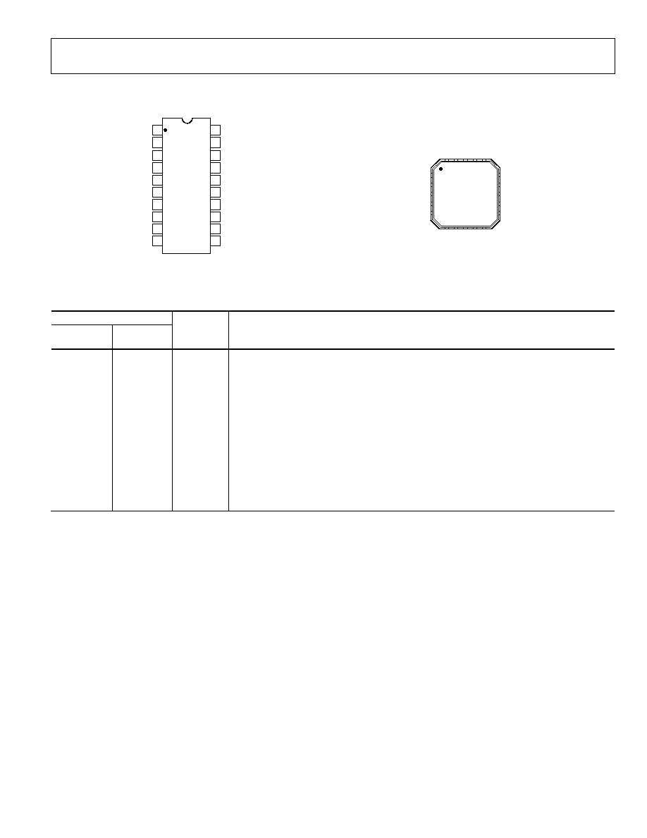
PIN CONFIGURATIONS AND FUNCTION DESCRIPTIONS
1
2
3
4
5
6
7
8
20
19
18
17
16
15
14
13
V
DD
GND
RF1A
GND
GND
RF1B
GND
GND
INA
GND
RF2A
GND
GND
RF2B
GND
ADG936
ADG936-R
TOP VIEW
(Not to Scale)
04503-0-002
RFCA
9
10
12
11
GND
RFCB
INB
GND
15
GND
14
RF2A
13
GND
12
GND
GND
1
RF1A
2
GND
3
GND
6
GND
7
RFCB
8
GND
9
GND
4
20
GND
18
RFC
A
17
GND
19
V
DD
ADG936
ADG936-R
TOP VIEW
(Not to Scale)
04503-0-003
INB
10
16
INA
11
RF2B
RF1B
5
Figure 5. 20-Lead TSSOP (RU-20)
Figure 6. 20-Lead 4 mm ◊ 4 mm LFCSP (CP-20)
Table 4. Pin Function Descriptions
Pin No.
20-Lead
TSSOP
20-Lead
LFCSP Mnemonic
Function
1
18
RFCA
Common RF Port for Switch A.
2 19
V
DD
Power Supply Input. These parts can be operated from 1.65 V to 2.75 V. V
DD
should be
decoupled to GND.
3, 5, 6, 8, 9,
11,13, 15,
16, 18, 20
1, 3, 4, 6, 7,
9, 12,13, 15,
17, 20
GND
Ground Reference Point for All Circuitry on the Part.
4
2
RF1A
RF1A Port.
7 5 RF1B
RF1B
Port.
10
8
RFCB
Common RF Port for Switch B.
12
10
INB
Logic Control Input.
14 11 RF2B
RF2B
Port.
17 14 RF2A
RF2A
Port.
19
16
INA
Logic Control Input.

ADG936/ADG936-R
Rev. 0 | Page 6 of 16
TERMINOLOGY
Table 5.
Parameter
Description
V
DD
Most Positive Power Supply Potential.
I
DD
Positive Supply Current.
GND
Ground (0 V) Reference.
INx
Logic Control Input.
V
INL
Maximum Input Voltage for Logic 0.
V
INH
Minimum Input Voltage for Logic 1.
I
INL
(I
INH
)
Input Current of the Digital Input.
C
IN
Digital Input Capacitance.
t
ON
Delay between Applying the Digital Control Input and the Output Switching On.
t
OFF
Delay between Applying the Digital Control Input and the Output Switching Off.
t
RISE
Rise Time. Time for the RF signal to rise from 10% of the On level to 90% of the On level.
t
FALL
Fall Time. Time for the RF signal to fall from 90% of the On level to 10% of the On level.
Off Isolation
The Attenuation between Input and Output Ports of the Switch when the Switch Control Voltage Is in the Off Condition.
Insertion Loss
The Attenuation between Input and Output Ports of the Switch when the Switch Control Voltage Is in the On Condition.
Crosstalk
Measure of Unwanted Signal Coupled through from One Channel to Another as a Result of Parasitic Capacitance.
P
≠1 dB
1 dB Compression Point. The RF input power level at which the switch insertion loss increases by 1 dB over its low level
value. P
≠1 dB
is a measure of how much power the On switch can handle before the insertion loss increases by 1 dB.
IP
3
Third-Order Intermodulation Intercept. This is a measure of the power in false tones that occurs when closely spaced
tones are passed through a switch, whereby the nonlinearity of the switch causes these false tones to be generated.
Return Loss
The Amount of Reflected Power Relative to the Incident Power at a Port. Large return loss indicates good matching. By
measuring return loss, the VSWR can be calculated from conversion charts. VSWR (voltage standing wave ratio) indicates
the degree of matching present at a switch RF port.
Video
Feedthrough
Spurious Signals Present at the RF Ports of the Switch when the Control Voltage Is Switched from High to Low or Low to
High without an RF Signal Present.
ADG936/ADG936-R
Rev. 0 | Page 7 of 16
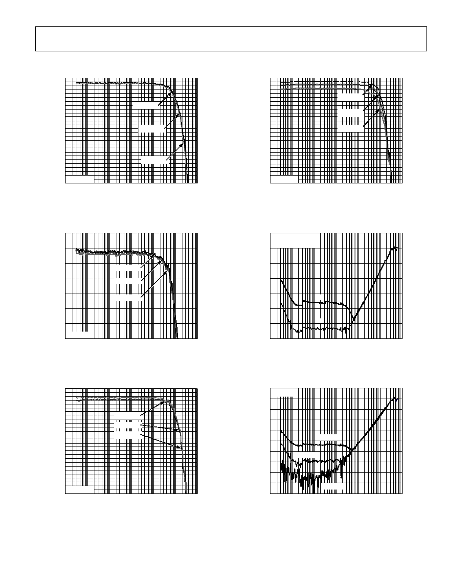
TYPICAL PERFORMANCE CHARACTERISTICS
04503-0-015
FREQUENCY (Hz)
10G
10k
100k
1M
10M
100M
1G
IN
SER
TION
LOSS (
d
B
)
≠0.3
≠0.4
≠0.5
≠0.6
≠0.7
≠0.8
≠0.9
≠1.0
≠1.1
≠1.2
≠1.3
≠1.4
≠1.5
≠1.6
≠1.7
≠1.8
≠1.9
≠2.0
≠2.1
≠2.2
≠2.3
≠2.4
≠2.5
≠2.6
≠2.7
≠2.8
≠2.9
≠3.0
V
DD
= 2.25V
V
DD
= 2.50V
V
DD
= 2.75V
T
A
= 25∞C
Figure 7. Insertion Loss vs. Frequency over Supplies
(S12 and S21)
04503-0-016
FREQUENCY (Hz)
10G
10k
100k
1M
10M
100M
1G
IN
SER
TION
LOSS (
d
B
)
≠0.3
≠0.5
≠0.4
≠0.6
≠0.7
≠0.8
≠0.9
≠1.0
V
DD
= 2.25V
V
DD
= 2.50V
V
DD
= 2.75V
T
A
= 25∞C
Figure 8. Insertion Loss vs. Frequency over Supplies
(S12 and S21)(Zoomed Figure 7)
FREQUENCY (Hz)
10G
10k
100k
1M
10M
100M
1G
IN
SER
TION
LOSS (
d
B
)
≠0.3
≠0.8
≠0.7
≠0.6
≠0.5
≠0.4
≠1.2
≠1.1
≠1.0
≠0.9
≠1.7
≠2.2
≠2.1
≠2.0
≠1.9
≠1.8
≠1.6
≠1.5
≠1.4
≠1.3
≠2.3
≠2.4
≠2.5
≠2.6
≠2.7
≠2.9
≠2.8
≠3.0
V
DD
= 1.65V
V
DD
= 1.80V
V
DD
= 1.95V
T
A
= 25∞C
04503-0-017
Figure 9. Insertion Loss vs. Frequency over Supplies
(S12 and S21)
04503-0-018
FREQUENCY (Hz)
10G
10k
100k
1M
10M
100M
1G
IN
SER
TION
LOSS (
d
B
)
≠0.3
≠0.8
≠0.7
≠0.6
≠0.5
≠0.4
≠1.2
≠1.1
≠1.0
≠0.9
≠1.7
≠2.2
≠2.1
≠2.0
≠1.9
≠1.8
≠1.6
≠1.5
≠1.4
≠1.3
≠2.3
≠2.4
≠2.5
≠2.6
≠2.7
≠2.9
≠2.8
≠3.0
V
DD
= 2.5V
T
A
= ≠40∞C
T
A
= +25∞C
T
A
= +85∞C
Figure 10. Insertion Loss vs. Frequency over Temperature
( S12 and S21)
04503-0-019
FREQUENCY (Hz)
10G
10k
100k
1M
10M
100M
1G
OFF IS
OLATION (dB)
≠10
≠20
≠30
≠40
≠50
≠60
≠70
≠80
S12
S21
V
DD
= 1.65V TO 2.75V
T
A
= 25∞C
Figure 11. Isolation vs. Frequency over Supplies
04503-0-020
FREQUENCY (Hz)
10G
1G
10k
100k
1M
10M
100M
OFF IS
OLATION (dB)
≠10
≠30
≠20
≠50
≠40
≠70
≠60
≠90
≠80
≠100
≠110
T
A
= ≠40∞C
T
A
= +85∞C
T
A
= +25∞C
V
DD
= 2.5V
Figure 12. Isolation vs. Frequency over Temperature

ADG936/ADG936-R
Rev. 0 | Page 8 of 16
04503-0-021
FREQUENCY (Hz)
10G
10k
100k
1M
10M
100M
1G
RE
TURN LOS
S
(dB)
0
≠5
≠10
≠15
≠20
≠25
≠30
V
DD
= 2.5V
T
A
= 25∞C
OFF SWITCH
ON SWITCH
Figure 13. Return Loss vs. Frequency ( S11)
04503-0-022
FREQUENCY (Hz)
10G
10k
100k
1M
10M
100M
1G
CROS
S
T
ALK (dB)
≠10
≠20
≠30
≠40
≠50
≠60
≠70
≠80
≠90
V
DD
= 2.5V
T
A
= 25∞C
Figure 14. Crosstalk vs. Frequency (S12 and S21)
04503-0-023
T
[
]
CH1
CH2
5.00ns
CH3
1.00V
100mV
100mV
1
3
TEK RUN: 5.00GS/s ET ENVELOPE
INx
RFx
Figure 15. Switch Timing
04503-0-024
CH3
1.00mV
CH1 1.00V
20.0ns
: 2.20mV
1
3
T
TEK RUN
[ ]
RFCx
INx
T
TRIG'D
Figure 16. Video Feedthrough
04504-0-019
FREQUENCY (MHz)
900
100
200
300
400
500
600
700
800
IP
3
(dB)
35
30
25
20
15
10
5
0
V
DD
= 2.5V
T
A
= 25∞C
Figure 17. IP
3
vs. Frequency
04503-0-025
FREQUENCY (MHz)
1500
0
250
500
750
1000
1250
P
≠1d
B
(dBm)
18
14
16
12
10
6
8
2
4
0
V
DD
= 2.5V
T
A
= 25∞C
Figure 18. P
≠1 dB
vs. Frequency
ADG936/ADG936-R
Rev. 0 | Page 9 of 16
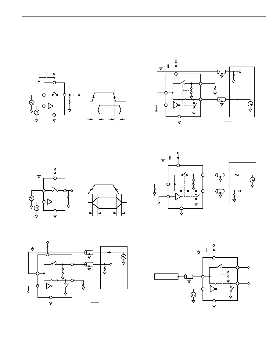
TEST CIRCUITS
Similar setup for the ADG936. Additional pins omitted for clarity.
t
ON
50%
50%
90%
10%
V
INx
V
OUT
t
OFF
10
µ
F
V
S
INx
RFx
RFCx
R
L
50
V
OUT
GND
V
DD
V
DD
04503-0-004
Figure 19. Switch Timing: t
ON
, t
OFF
V
INx
V
OUT
50%
50%
90%
90%
10%
10%
t
FALL
t
RISE
V
DD
V
DD
10
µ
F
V
S
INx
RFx
RFCx
GND
R
L
50
V
OUT
04503-0-005
Figure 20. Switch Timing: t
RISE
, t
FALL
V
S
NETWORK
ANALYZER
V
INx
OFF ISOLATION = 20log
V
OUT
V
S
V
DD
10
µ
F
V
DD
50
V
OUT
R
L
50
ADG936-R
RF2x
RF1x
INx
RFC
GND
50
04503-0-006
Figure 21. Off Isolation
V
S
NETWORK
ANALYZER
V
INx
INSERTION LOSS = 20log
V
OUT
V
S
V
DD
10
µ
F
V
DD
50
V
OUT
R
L
50
ADG936-R
RF2x
RF1x
INx
RFCx
GND
50
04503-0-007
Figure 22. Insertion Loss
V
S
NETWORK
ANALYZER
V
INx
CROSSTALK = 20log
V
OUT
V
S
V
DD
10
µ
F
V
DD
50
V
OUT
R
L
50
ADG936-R
RF2x
RF1x
INx
RFCx
GND
50
04503-0-008
Figure 23. Crosstalk
V
INx
V
DD
10
µ
F
V
DD
ADG936-R
RF2x
RF1x
INx
RFCx
NC
NC
OSCILLOSCOPE
GND
04503-0-009
Figure 24. Video Feedthrough
ADG936/ADG936-R
Rev. 0 | Page 10 of 16
SPECTRUM
ANALYZER
V
INx
V
DD
10
µ
F
V
DD
ADG936-R
RF2x
RF1x
INx
RFCx
GND
50
COMBINER
RF
SOURCE
RF
SOURCE
04503-0-010
Figure 25. IP
3
SPECTRUM
ANALYZER
V
INx
V
DD
10
µ
F
V
DD
ADG936-R
RF2x
RF1x
INx
RFCx
GND
50
RF
SOURCE
V
S
04503-0-011
Figure 26. P
≠1 dB
ADG936/ADG936-R
Rev. 0 | Page 11 of 16
APPLICATIONS
The ADG936/ADG936-R are ideal solutions for low power,
high frequency applications. The low insertion loss, high
isolation between ports, low distortion, and low current
consumption of these parts make them excellent solutions for
many high frequency switching applications. They can be used
in applications such as switchable filters, transmitters and
receivers for radar systems, and communication systems from
base stations to cell phones.
The ADG9xx family of wideband switches is designed to meet
the demands of devices transmitting at ISM band frequencies to
1 GHz and higher. The low insertion loss, high isolation
between ports, single pin control interface, no requirement for
dc blocking capacitors, and TTL interface compatibility make
them cost-effective and easy-to-integrate switching solutions for
many high frequency switching and low power applications,
because the parts can handle up to 16 dBm of power.
ABSORPTIVE VS. REFLECTIVE
The ADG936 is an absorptive (matched) switch with 50
terminated shunt legs; the ADG936-R is a reflective switch with
0 terminated shunts to ground. The ADG936 absorptive
switch has a good VSWR on each port, regardless of the switch
mode. An absorptive switch should be used when there is a
need for a good VSWR that is looking into the port but not
passing the through-signal to the common port. The ADG936
is, therefore, ideal for applications that require minimum
reflections back to the RF source. It also ensures that the
maximum power is transferred to the load.
The ADG936-R reflective switch is suitable for applications in
which high off-port VSWR does not matter, and the switch has
some other desired performance features. It can be used in
many applications, including high speed filter selection. In most
cases, an absorptive switch can be used instead of a reflective
switch, but not vice versa.
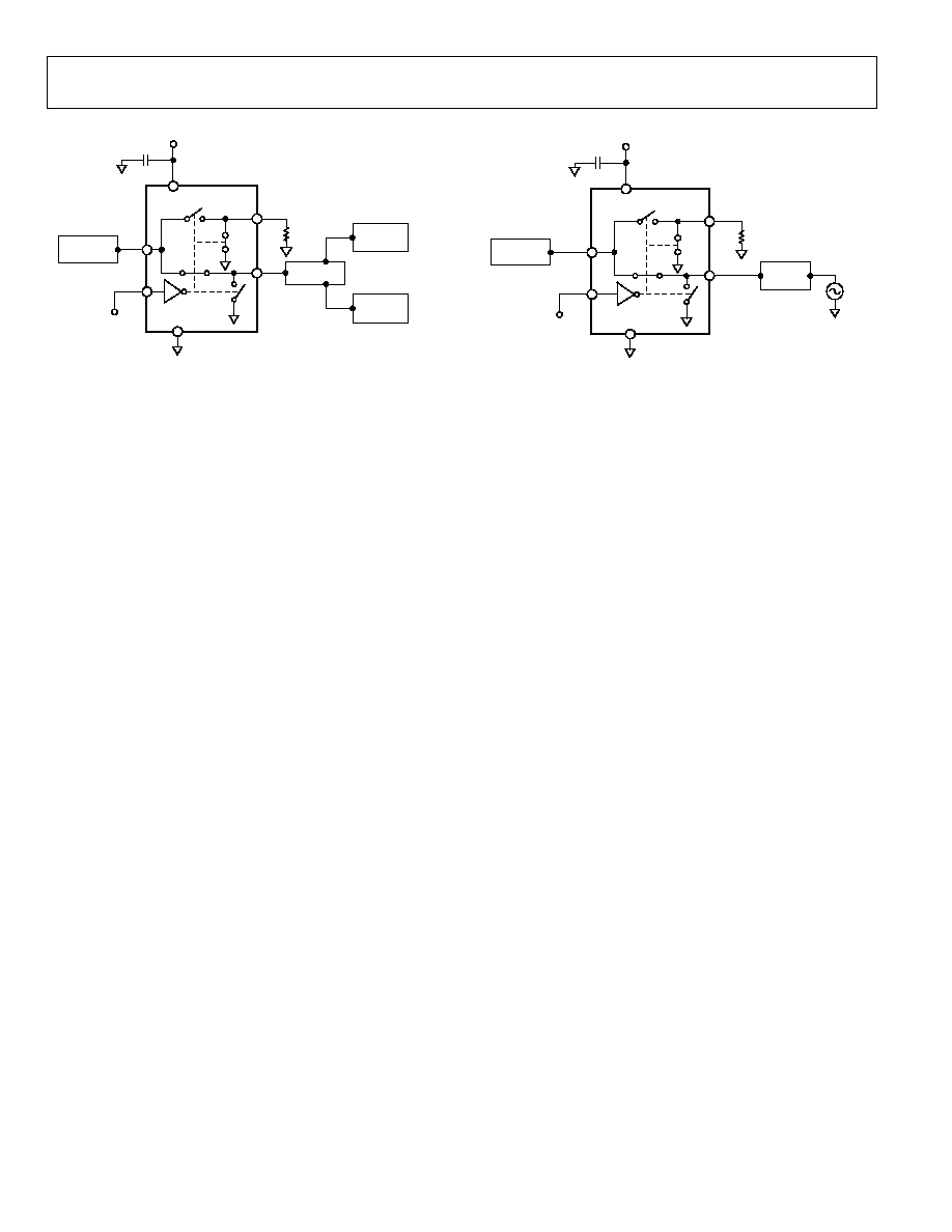
FILTER SELECTION
The ADG936 and ADG936-R can be used to switch high
frequency signals between different filters, and to multiplex the
signal to the output. These dual SPDT switches are also ideal for
high speed signal routing and for switching high speed
differential signals.
ADG936
ADG936
RF1A
RF2A
RF1B
RF2B
RF1A
RF2A
RF1B
RF2B
RF
OUT
RFCA
RF
OUT
RFCB
RF
IN
RFCB
RF
IN
RFCA
04504-0-013
Figure 27. Filter Selection
Tx/Rx SWITCHING
The low insertion loss and high isolation between ports ensure
that the ADG936/ADG936-R are suitable transmit/receive
switches for all ISM band and Wireless LAN applications,
providing the required isolation between the transmit and
receive signals.
ANTENNA
ADG936
RF1B
RF2B
RF1B
RF2B
RFCB
RFCA
PA
LNA
04504-0-014
Figure 28. Tx/Rx Switching
ANTENNA DIVERSITY SWITCH
The ADG936/ADG936-R are ideal for use as antenna diversity
switches, switching in different antennas to the tuner. The low
insertion loss, which ensures minimum signal loss and high
isolation between channels, makes these dual SPDT switches
suitable for switching applications in tuner modules and set-top
boxes.

ADG936/ADG936-R
Rev. 0 | Page 12 of 16
EVALUATION BOARD
The ADG936 and ADG936-R evaluation board allows
designers to evaluate these high performance wideband
switches with minimal effort.
To prove that these devices meet the user's requirements, only a
power supply and a network analyzer, along with the evaluation
board, are required. An application note available with the
evaluation board gives complete information on operating the
evaluation board.
The RFCA port is connected through a 50 transmission line
to SMA connector J3. The RFCB port is connected through a
50 transmission line to SMA connector J4. RF1A, RF2A,
RF1B, and RF2B are connected through 50 transmission lines
to SMA connectors J5, J6, J7, and J8, respectively. A through
transmission line connects J9 and J10; this transmission line is
used to estimate the loss of the PCB over the environmental
conditions being evaluated.
The board is constructed of a four-layer, FR4 material with a
dielectric constant of 4.3 and an overall thickness of 0.062 in.
Two ground layers with grounded planes provide ground for
the RF transmission lines. The transmission lines were designed
using a coplanar waveguide with ground plane model using a
trace width of 0.024 in, clearance to ground plane of 0.008 in,
dielectric thickness of 0.02 in, and a metal thickness of
0.0021 in.
Figure 29. ADG936 and ADG936-R Evaluation Board Top View
ADG936/ADG936-R
Rev. 0 | Page 13 of 16
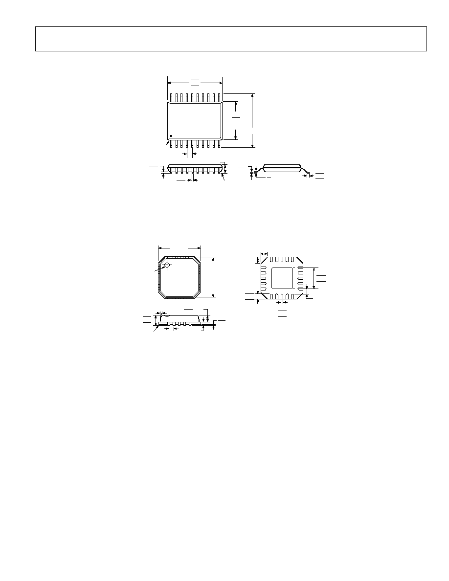
OUTLINE DIMENSIONS
20
1
11
10
6.40 BSC
4.50
4.40
4.30
PIN 1
6.60
6.50
6.40
SEATING
PLANE
0.15
0.05
0.30
0.19
0.65
BSC
1.20 MAX
0.20
0.09
0.75
0.60
0.45
8∞
0∞
COMPLIANT TO JEDEC STANDARDS MO-153AC
COPLANARITY
0.10
Figure 30. 20-Lead Thin Shrink Small Outline Package [TSSOP]
(RU-20)
Dimensions shown in millimeters
1
20
5
6
11
16
15
10
2.25
2.10 SQ
1.95
0.75
0.55
0.35
0.30
0.23
0.18
0.50
BSC
12∞ MAX
0.20
REF
0.80 MAX
0.65 TYP
0.05 MAX
0.02 NOM
1.00
0.85
0.80
SEATING
PLANE
PIN 1
INDICATOR
TOP
VIEW
3.75
BCS SQ
4.00
BSC SQ
COPLANARITY
0.08
0.60
MAX
0.60
MAX
0.25 MIN
EXPOSED
PAD
(BOTTOM VIEW)
COMPLIANT TO JEDEC STANDARDS MO-220-VGGD-1
Figure 31. 20-Lead Lead Frame Chip Scale Package [LFCSP] 4 mm ◊ 4 mm Body
(CP-20-1)
Dimensions shown in millimeters

ADG936/ADG936-R
Rev. 0 | Page 14 of 16
ORDERING GUIDE
Model
Temperature Range
Package Description
Package Option
ADG936BRU
≠40∞C to +85∞C
Thin Shrink Small Outline Package (TSSOP)
RU-20
ADG936BRU-500RL7
≠40∞C to +85∞C
Thin Shrink Small Outline Package (TSSOP)
RU-20
ADG936BRU-REEL
≠40∞C to +85∞C
Thin Shrink Small Outline Package (TSSOP)
RU-20
ADG936BRU-REEL7
≠40∞C to +85∞C
Thin Shrink Small Outline Package (TSSOP)
RU-20
ADG936BCP
≠40∞C to +85∞C
Lead Frame Chip Scale Package (LFCSP)
CP-20-1
ADG936BCP-500RL7
≠40∞C to +85∞C
Lead Frame Chip Scale Package (LFCSP)
CP-20-1
ADG936BCP-REEL
≠40∞C to +85∞C
Lead Frame Chip Scale Package (LFCSP)
CP-20-1
ADG936BCP-REEL7
≠40∞C to +85∞C
Lead Frame Chip Scale Package (LFCSP)
CP-20-1
ADG936BRU-R
≠40∞C to +85∞C
Thin Shrink Small Outline Package (TSSOP)
RU-20
ADG936BRU-R-500RL7
≠40∞C to +85∞C
Thin Shrink Small Outline Package (TSSOP)
RU-20
ADG936BRU-R-REEL
≠40∞C to +85∞C
Thin Shrink Small Outline Package (TSSOP)
RU-20
ADG936BRU-R-REEL7
≠40∞C to +85∞C
Thin Shrink Small Outline Package (TSSOP)
RU-20
ADG936BCP-R
≠40∞C to +85∞C
Lead Frame Chip Scale Package (LFCSP)
CP-20-1
ADG936BCP-R-500RL7
≠40∞C to +85∞C
Lead Frame Chip Scale Package (LFCSP)
CP-20-1
ADG936BCP-R-REEL
≠40∞C to +85∞C
Lead Frame Chip Scale Package (LFCSP)
CP-20-1
ADG936BCP-R-REEL7
≠40∞C to +85∞C
Lead Frame Chip Scale Package (LFCSP)
CP-20-1
EVAL-ADG936EB
Evaluation
Board
RU-20
EVAL-ADG936-REB
Evaluation
Board
RU-20

ADG936/ADG936-R
Rev. 0 | Page 15 of 16
NOTES

ADG936/ADG936-R
Rev. 0 | Page 16 of 16
NOTES
© 2004 Analog Devices, Inc. All rights reserved. Trademarks and
registered trademarks are the property of their respective owners.
D04503≠0≠7/04(0)