Complete Thermal System
Management Controller
ADM1026
Rev. A
Information furnished by Analog Devices is believed to be accurate and reliable.
However, no responsibility is assumed by Analog Devices for its use, nor for any
infringements of patents or other rights of third parties that may result from its use.
Specifications subject to change without notice. No license is granted by implication
or otherwise under any patent or patent rights of Analog Devices. Trademarks and
registered trademarks are the property of their respective owners.
One Technology Way, P.O. Box 9106, Norwood, MA 02062-9106, U.S.A.
Tel: 781.329.4700
www.analog.com
Fax: 781.326.8703
© 2004 Analog Devices, Inc. All rights reserved.
FEATURES
Up to 19 analog measurement channels (including internal
measurements)
Up to 8 fan speed measurement channels
Up to 17 general-purpose logic I/O pins
Remote temperature measurement with remote diode (two
channels)
On-chip temperature sensor
Analog and PWM fan speed control outputs
2-wire serial system management bus (SMBus)
8 kB on-chip EEPROM
Full SMBus 1.1 support includes packet error checking (PEC)
Chassis intrusion detection
Interrupt output (SMBAlert)
Reset input, reset outputs
Thermal interrupt (THERM) output
Limit comparison of all monitored values
APPLICATIONS
Network servers and personal computers
Telecommunications equipment
Test equipment and measuring instruments
D2≠/A
IN9
(0V ≠ +2.5V)
D2+/A
IN8
(0V ≠ +2.5V)
A
IN7
(0V ≠ +2.5V)
A
IN6
(0V ≠ +2.5V)
TO GPIO
REGISTERS
100k
100k
V
CC
V
CC
V
CC
FAN
SPEED
COUNTER
INPUT
ATTENUATORS
AND
ANALOG
MULTIPLEXER
GPIO
REGISTERS
SERIAL BUS
INTERFACE
ADDRESS
POINTER
REGISTER
BAND GAP
TEMPERATURE
SENSOR
AUTOMATIC
FAN SPEED
CONTROL
8k BYTES
EEPROM
8-BIT
ADC
BAND GAP
REFERENCE
V
BAT
+5 V
IN
≠12 V
IN
+12 V
IN
+V
CCP
A
IN0
(0V ≠ +3V)
A
IN1
(0V ≠ +3V)
A
IN2
(0V ≠ +3V)
A
IN3
(0V ≠ +3V)
A
IN4
(0V ≠ +3V)
A
IN5
(0V ≠ +3V)
D1+
D1≠/NTESTIN
DGND
DAC
AGND
V
REF
(1.82V OR 2.5V)
SCL
SDA
3.3V MAIN
ADD/
NTESTOUT
FAN7/GPIO7
FAN6/GPIO6
FAN5/GPIO5
FAN4/GPIO4
FAN3/GPIO3
FAN2/GPIO2
FAN1/GPIO1
FAN0/GPIO0
GPIO15
GPIO14
GPIO13
GPIO12
GPIO11
GPIO10
GPIO9
GPIO8
PWM
3.3V STBY
GPIO16/THERM
CI
ADM1026
INT
RESET IN
V
CC
V
CC
100k
RESETMAIN
RESETSTBY
PWM REGISTER
AND CONTROLLER
LIMIT
COMPARATORS
INT MASK
REGISTERS
INTERRUPT
MASKING
CONFIGURATION
REGISTERS
VALUE AND
LIMIT
REGISTERS
3.3V MAIN
RESET
GENERATOR
3.3V STBY
RESET
GENERATOR
INTERRUPT
STATUS
REGISTERS
ANALOG
OUTPUT REGISTER
AND 8-BIT DAC
02657-A
-
001
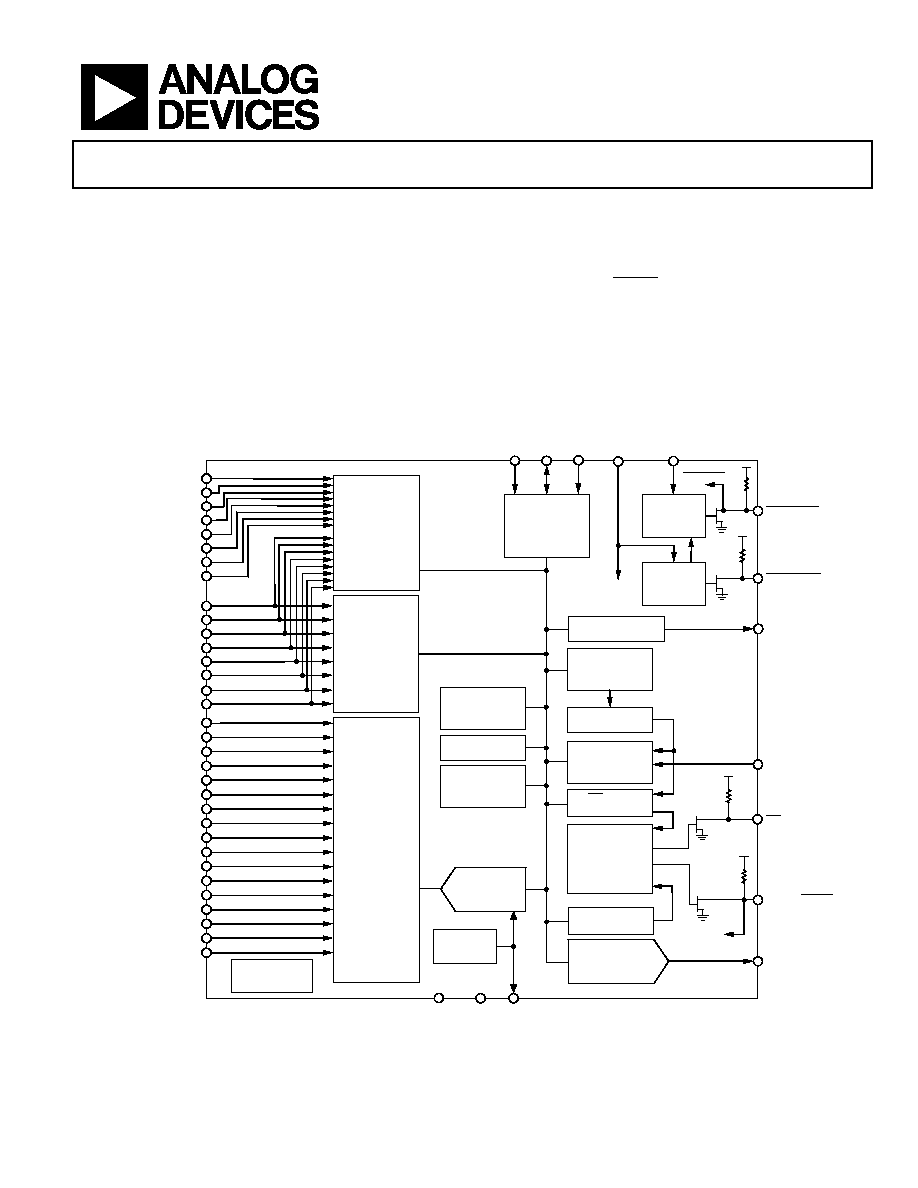
Figure 1. Functional Block Diagram

ADM1026
Rev. A | Page 2 of 56
TABLE OF CONTENTS
Specifications..................................................................................... 3
Absolute Maximum Ratings............................................................ 5
Thermal Characteristics .............................................................. 5
ESD Caution.................................................................................. 5
Pin Configuration and Function Descriptions............................. 6
Typical Performance Characteristics ............................................. 8
Product Description ....................................................................... 10
Functional Description.............................................................. 10
Internal Registers........................................................................ 11
EEPROM ..................................................................................... 11
SMBus Protocols for RAM and EEPROM .............................. 13
Measurement Inputs .................................................................. 16
Temperature Measurement System.......................................... 20
Analog Output ............................................................................ 22
Fan Speed Measurement ........................................................... 25
Enabling and Clearing Interrupts ............................................ 29
NAND Tree Tests........................................................................ 31
Using the ADM1026 .................................................................. 33
Registers........................................................................................... 36
Detailed Register Descriptions ................................................. 38
Outline Dimensions ....................................................................... 54
Ordering Guide .......................................................................... 55
REVISION HISTORY
3/04--Data Sheet Changed from Rev. 0 to Rev. A
Updated Format..................................................................Universal
Change to Footnote 4, Table 1..........................................................4
Added Figure 15.................................................................................9
Changes to Table 6.......................................................................... 17
Changes to Figure 27...................................................................... 18
Change to Figure 31 ....................................................................... 19
Change to Battery Measurement Input Section ......................... 19
Changes to Table 7.......................................................................... 21
Changes to Equations in Fan Speed Measurement Section...... 26
Change to Chassis Intrusion Input Section ................................ 27
Changes to Reset Input and Outputs Section ............................. 31
Changes to Software Reset Function Section ............................. 34
Changes to Ordering Guide .......................................................... 55
5/02--Revision 0: Initial Version

ADM1026
Rev. A | Page 3 of 56
SPECIFICATIONS
1,
2,
3
Table 1. T
A
= T
MIN
to T
MAX
, V
CC
= V
MIN
to V
MAX
, unless otherwise noted.
Parameter
Min
Typ
Max
Test Conditions/Comments
Unit
POWER
SUPPLY
Supply Voltage, 3.3 V STBY, 3.3 V MAIN
3.0
3.3
5.5
V
Supply Current, I
CC
2.5
4.0
Interface inactive, ADC active
mA
TEMPERATURE-TO-DIGITAL
CONVERTER
Internal
Sensor
Accuracy
±3
∞C
Resolution
±1
∞C
External Diode Sensor Accuracy
±3
0∞C < T
D
< 100∞C
∞C
Resolution
±1
∞C
Remote Sensor Source Current
90
High level
µA
5.5
Low
level
µA
ANALOG-TO-DIGITAL CONVERTER (including MUX and attenuators)
Total Unadjusted Error (TUE)
4
±2
%
Differential Nonlinearity (DNL)
±1
LSB
Power Supply Sensitivity
±0.1
%/V
Conversion Time (Analog Input or Internal Temperature)
5
11.38
12.06
ms
Conversion Time (External Temperature)
5
34.13
36.18
ms
Input Resistance (+5 V
IN
, V
CCP
, A
IN0
- A
IN5
)
80
100
120
k
Input Resistance of +12 V
IN
pin
70
100
115
k
Input Resistance of -12 V
IN
pin
8
10
12
k
Input Resistance (A
IN6
- A
IN9
)
5
M
Input Resistance of V
BAT
pin
4
80
100
120
k
V
BAT
Current Drain (when measured)
80
100
CR2032 battery life >10 years
nA
V
BAT
Current Drain (when not measured)
6
nA
ANALOG OUTPUT (DAC)
Output Voltage Range
0≠2.5
V
Total Unadjusted Error (TUE)
±5
I
L
= 2 mA
%
Zero Error
1
No load
LSB
Differential Nonlinearity (DNL)
±1
Monotonic by design
LSB
Integral Nonlinearity
±0.5
LSB
Output Source Current
2
mA
Output Sink Current
1
mA
REFERENCE OUTPUT
Output Voltage
1.8
1.82
1.84
Bit 2 of Register 07h = 0
V
Output Voltage
2.47
2.50
2.53
Bit 2 of Register 07h = 1
V
Load Regulation (I
SINK
= 2 mA)
0.15
%
Load Regulation (I
SOURCE
= 2 mA)
0.15
%
Short Circuit Current
25
V
CC
= 3.3 V
mA
Output Current Source
2
mA
Output Current Sink
2
mA
FAN RPM-TO-DIGITAL CONVERTER
6
Accuracy
±12
%
Full-Scale Count
255
FAN0 to FAN7 Nominal Input RPM
5
8800
Divisor = 1, fan count = 153
RPM
4400
Divisor = 2, fan count = 153
RPM
2200
Divisor = 4, fan count = 153
RPM
1100
Divisor = 8, fan count = 153
RPM
Internal Clock Frequency
20
22.5
25
kHz
OPEN DRAIN O/Ps, PWM, GPIO0 to 16
Output High Voltage, V
OH
2.4
I
OUT
= 3.0 mA, V
CC
= 3.3 V
V

ADM1026
Rev. A | Page 4 of 56
Parameter
Min
Typ
Max
Test Conditions/Comments
Unit
High Level Output Leakage Current, I
OH
0.1
1
V
OUT
= V
CC
µA
Output Low Voltage, V
OL
0.4
I
OUT
= -3.0 mA, V
CC
= 3.3 V
V
PWM Output Frequency
75
Hz
DIGITAL OUTPUTS (INT, RESETMAIN, RESETBY)
Output Low Voltage, V
OL
0.4
I
OUT
= -3.0 mA, V
CC
= 3.3 V
V
RESET Pulse Width
140 180 240
ms
OPEN DRAIN SERIAL DATABUS OUTPUT (SDA)
Output Low Voltage, V
OL
0.4
I
OUT
= ≠3.0 mA, V
CC
= 3.3 V
V
High Level Output Leakage Current, I
OH
0.1
1
V
OUT
= V
CC
µA
SERIAL BUS DIGITAL INPUTS (SCL, SDA)
Input High Voltage, V
IH
2.2
V
Input Low Voltage, V
IL
0.8
V
Hysteresis
500
mV
DIGITAL INPUT LOGIC LEVELS (ADD, CI, FAN 0 to 7, GPIO 0 to 16)
7,
8
Input High Voltage, V
IH
2.4
V
CC
= 3.3 V
V
Input Low Voltage, V
IL
0.8
V
CC
= 3.3 V
V
Hysteresis (Fan 0 to 7)
250
V
CC
= 3.3 V
mV
RESETMAIN, RESETSTBY
RESETMAIN Threshold
2.89
2.94
2.97
Falling voltage
V
RESETSBY Threshold
3.01
3.05
3.10
Falling voltage
V
RESETMAIN Hysteresis
60
mV
RESETSTBY Hysteresis
70
mV
DIGITAL
INPUT
CURRENT
Input High Current, I
IH
≠1
V
IN
= V
CC
µA
Input Low Current, I
IL
1
V
IN
= 0
µA
Input Capacitance, C
IN
20
pF
EEPROM
RELIABILITY
Endurance
9
100
700
kcycles
Data Retention
10
10
Years
SERIAL BUS TIMING
See Figure 2 for all parameters.
Clock Frequency, f
SCLK
400
kHz
Glitch Immunity, t
SW
50
ns
Bus Free Time, t
BUF
4.7
µs
Start Setup Time, t
SU; STA
4.7
µs
Start Hold Time, t
HD; STA
4
µs
SCL Low Time, t
LOW
4.7
µs
SCL High Time, t
HIGH
4
µs
SCL, SDA Rise Time, t
r
1000
ns
SCL, SDA Fall Time, t
f
300
ns
Data Setup Time, t
SU; DAT
250
ns
Data Hold Time, t
HD; DAT
300
ns
1
All voltages are measured with respect to GND, unless otherwise specified.
2
Typicals are at T
A
= 25∞C and represent the most likely parametric norm. Shutdown current typ is measured with V
CC
= 3.3 V.
3
Timing specifications are tested at logic levels of V
IL
= 0.8 V for a falling edge and V
IH
= 2.1 V for a rising edge.
4
Total unadjusted error (TUE) includes offset, gain, and linearity errors of the ADC, multiplexer, and on-chip input attenuators. V
BAT
is accurate only for V
BAT
voltages
greater than 1.5 V (see Figure 15).
5
Total analog monitoring cycle time is nominally 273 ms, made up of 18 ms ◊ 11.38 ms measurements on analog input and internal temperature channels, and
2 ms ◊ 34.13 ms measurements on external temperature channels.
6
The total fan count is based on two pulses per revolution of the fan tachometer output. The total fan monitoring time depends on the number of fans connected and
the fan speed. See the Fan Speed Measurement section for more details.
7
ADD is a three-state input that may be pulled high, low, or left open-circuit.
8
Logic inputs accept input high voltages up to 5 V even when device is operating at supply voltages below 5 V.
9
Endurance is qualified to 100,000 cycles as per JEDEC Std. 22 method A117, and measured at -40∞C, +25∞C, and +85∞C. Typical endurance at +25∞C is 700,000 cycles.
10
Retention lifetime equivalent at junction temperature (T
J
) = 55∞C as per JEDEC Std. 22 method A117. Retention lifetime based on an activation energy of 0.6 V
derates with junction temperature as shown in Figure 16.
ADM1026
Rev. A | Page 5 of 56
ABSOLUTE MAXIMUM RATINGS
Table 2.
Parameter Rating
Positive Supply Voltage (V
CC
) 6.5
V
Voltage on +12 V V
IN
Pin
+20 V
Voltage on -12 V V
IN
Pin
-20 V
Voltage on Analog Pins
-0.3 V to (V
CC
+ 0.3 V)
Voltage on Open Drain Digital Pins
-0.3 V to +6.5 V
Input Current at any Pin
±5 mA
Package Input Current
±20 mA
Maximum Junction Temperature (T
J
MAX
) 150∞C
Storage Temperature Range
-65∞C to +150∞C
Lead Temperature, Soldering
Vapor Phase (60 sec)
215∞C
Infrared (15 sec)
200∞C
ESD Rating, -12 V
IN
Pin
1000 V
ESD Rating, All Other Pins
2000 V
Stresses above those listed under Absolute Maximum Ratings
may cause permanent damage to the device. This is a stress
rating only; functional operation of the device at these or any
other conditions above those indicated in the operational
section of this specification is not implied. Exposure to absolute
maximum rating conditions for extended periods may affect
device reliability.
THERMAL CHARACTERISTICS
∑
48-Lead LQFP package
∑
JA
= 50∞C/W,
JC
= 10∞C/W
P
S
t
SU; DAT
t
HIGH
t
F
t
HD; DAT
t
R
t
LOW
t
SU; STO
P
S
SCL
SDA
t
BUF
t
HD; STA
t
HD; STA
t
SU; STA
02657-A
-
002
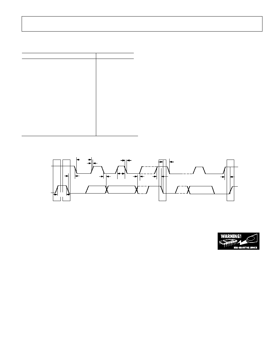
Figure 2. Serial Bus Timing Diagram
ESD CAUTION
ESD (electrostatic discharge) sensitive device. Electrostatic charges as high as 4000 V readily accumulate on
the human body and test equipment and can discharge without detection. Although this product features
proprietary ESD protection circuitry, permanent damage may occur on devices subjected to high energy
electrostatic discharges. Therefore, proper ESD precautions are recommended to avoid performance
degradation or loss of functionality.
ADM1026
Rev. A | Page 6 of 56
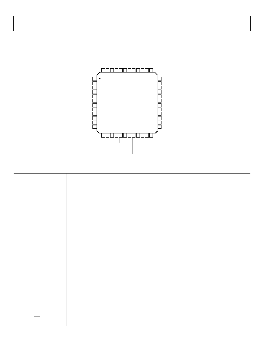
PIN CONFIGURATION AND FUNCTION DESCRIPTIONS
36
35
34
33
32
31
30
29
28
27
26
25
48
47
46
45
44
43
42
41
40
39
38
37
13
14
15
16
17
18
19
20
21
22
23
24
ADM1026
TOP VIEW
(Not to Scale)
PIN 1 IDENTIFIER
GPIO9
GPIO8
FAN0/GPIO0
FAN1/GPIO1
FAN2/GPIO2
FAN3/GPIO3
3.3V MAIN
DGND
FAN4/GPIO4
FAN5/GPIO5
FAN6/GPIO6
FAN7/GPIO7
SC
L
SD
A
ADD/NTE
S
TOUT
CI
INT
PW
M
R
ESETSTB
Y
R
ESETM
A
IN
AGND
3.3V STB
Y
DAC
V
RE
F
A
IN5
(0V ≠ 3V)
A
IN6
(0V ≠ 2.5V)
A
IN7
(0V ≠ 2.5V)
+V
CCP
+12 V
IN
≠12 V
IN
+5 V
IN
V
BAT
D2+/A
IN8
(0V ≠ 2.5V)
D2≠/A
IN9
(0V ≠ 2.5V)
D1+
D1≠/NTESTIN
GPIO10
GPIO11
GPIO12
GPIO13
GPIO14
GPIO15
GPIO16/
TH
ER
M
A
IN0
(0
V
≠
3
V
)
A
IN1
(0
V
≠
3
V
)
A
IN2
(0
V
≠
3
V
)
A
IN3
(0
V
≠
3
V
)
A
IN4
(0
V
≠
3
V
)
1
2
3
4
5
6
7
8
9
10
11
12
02657-A
-
003
Figure 3. Pin Configuration
Table 3.
Pin No.
Mnemonic
Type
Description
1
GPIO9
Digital I/O
1
General-purpose I/O pin that can be configured as digital inputs or outputs.
2
GPIO8
Digital I/O
1
General-purpose I/O pin that can be configured as digital inputs or outputs.
3
FAN0/GPIO0
Digital I/O
Fan tachometer input with internal 10 k pull-up resistor to 3.3 V STBY. Can be
reconfigured as a general-purpose, open drain, digital I/O pin.
4
FAN1/GPIO1
Digital I/O
Fan tachometer input with internal 10 k pull-up resistor to 3.3 V STBY. Can be
reconfigured as a general-purpose, open drain, digital I/O pin.
5
FAN2/GPIO2
Digital I/O
Fan tachometer input with internal 10 k pull-up resistor to 3.3 V STBY. Can be
reconfigured as a general-purpose, open drain, digital I/O pin.
6
FAN3/GPIO3
Digital I/O
Fan tachometer input with internal 10 k pull-up resistor to 3.3 V STBY. Can be
reconfigured as a general-purpose, open drain, digital I/O pin.
7
3.3 V MAIN
Analog Input
Monitors the main 3.3 V system supply. Does not power the device.
8
DGND
Ground
Ground pin for digital circuits.
9
FAN4/GPIO4
Digital I/O
Fan tachometer input with internal 10 k pull-up resistor to 3.3 V STBY. Can be
reconfigured as a general-purpose, open drain, digital I/O pin.
10
FAN5/GPIO5
Digital I/O
Fan tachometer input with internal 10 k pull-up resistor to 3.3 V STBY. Can be
reconfigured as a general-purpose, open drain, digital I/O pin.
11
FAN6/GPIO6
Digital I/O
Fan tachometer input with internal 10 k pull-up resistor to 3.3 V STBY. Can be
reconfigured as a general-purpose, open drain, digital I/O pin.
12
FAN7/GPIO7
Digital I/O
Fan tachometer input with internal 10 k pull-up resistor to 3.3 V STBY. Can be
reconfigured as a general-purpose, open drain, digital I/O pin.
13
SCL
Digital Input
Open Drain Serial Bus Clock. Requires a 2.2 k pull-up resistor.
14
SDA
Digital I/O
Serial Bus Data. Open drain I/O. Requires a 2.2 k pull-up resistor.
15
ADD/NTESTOUT
Digital Input
This is a three-state input that controls the two LSBs of the serial bus address. It also
functions as the output for NAND tree testing.
16
CI
Digital Input
An active high input that captures a chassis intrusion event in Bit 6 of Status Register 4.
This bit remains set until cleared, as long as battery voltage is applied to the V
BAT
input,
even when the ADM1026 is powered off.
17
INT
Digital Output
Interrupt Request (Open Drain). The output is enabled when Bit 1 of the configuration
register is set to 1. The default state is disabled. It has an on-chip 100 k pull-up resistor.

ADM1026
Rev. A | Page 7 of 56
Pin No.
Mnemonic
Type
Description
18
PWM
Digital Output
Open drain pulse width modulated output for control of the fan speed. This pin defaults
to high for the 100% duty cycle for use with NMOS drive circuitry. If a PMOS device is used
to drive the fan, the PWM output may be inverted by setting Bit 1 of Test Register 1 = 1.
19
RESETSTBY
Digital Output
Power-On Reset. 5 mA driver (weak 100 k pull-up), active low output (100 k pull-up)
with a 180 ms typical pulse width. RESETSTBY is asserted whenever 3.3 V STBY is below
the reset threshold. It remains asserted for approximately 180 ms after 3.3 V STBY rises
above the reset threshold.
20
RESETMAIN
Digital I/O
Power-On Reset. 5 mA driver (weak 100 k pull-up), active low output (100 k pull-up)
with a 180 ms typical pulse width. RESETMAIN is asserted whenever 3.3 V MAIN is below
the reset threshold. It remains asserted for approximately 180 ms after 3.3 V MAIN rises
above the reset threshold. If, however, 3.3 V STBY rises with or before 3.3 V MAIN, then
RESETMAIN remains asserted for 180 ms after RESETSTBY is deasserted. Pin 20 also
functions as an active low RESET input.
21
AGND
Ground
Ground pin for analog circuits.
22
3.3 V STBY
Power Supply
Supplies 3.3 V power. Also monitors the 3.3 V standby power rail.
23
DAC
Analog Output 0 V to 2.5 V output for analog control of the fan speed.
24
V
REF
Analog Output Reference Voltage Output. Can be selected as 1.8 V (default) or 2.5 V.
25
D1≠/NTESTIN
Analog Input
Connected to a cathode of the first remote temperature sensing diode. If it is held high at
power-on, it activates the NAND tree test mode.
26
D1+
Analog Input
Connected to the anode of the first remote temperature sensing diode.
27
D2≠/A
IN9
Programmable Connected to the cathode of the second remote temperature sensing diode, or the
analog input may be reconfigured as a 0 V- 2.5 V analog input.
28
D2+/A
IN8
Programmable Connected to the anode of the second remote temperature sensing diode, or the analog
input may be reconfigured as a 0 V - 2.5 V analog input.
29
V
BAT
Analog Input
Monitors battery voltage, nominally +3 V.
30
+5 V
IN
Analog Input
Monitors the +5 V supply.
31
-12 V
IN
Analog Input
Monitors the
-12 V supply.
32
+12 V
IN
Analog Input
Monitors the +12 V supply.
33
+V
CCP
Analog Input
Monitors the processor core voltage (0 V to 3.0 V).
34
A
IN7
Analog Input
General-purpose 0 V to 2.5 V analog inputs.
35
A
IN6
Analog Input
General-purpose 0 V to 2.5 V analog inputs.
36
A
IN5
Analog Input
General-purpose 0 V to 3 V analog inputs.
37
A
IN4
Analog Input
General-purpose 0 V to 3 V analog inputs.
38
A
IN3
Analog Input
General-purpose 0 V to 3 V analog inputs.
39
A
IN2
Analog Input
General-purpose 0 V to 3 V analog inputs.
40
A
IN1
Analog Input
General-purpose 0 V to 3 V analog inputs.
41
A
IN0
Analog Input
General-purpose 0 V to 3 V analog inputs.
42
GPIO16/THERM
Digital I/O
1
General-purpose I/O pin that can be configured as a digital input or output. Can also be
configured as a bidirectional THERM pin (100 k pull-up).
43
GPIO15
Digital I/O
1
General-purpose I/O pin that can be configured as a digital input or output.
44
GPIO14
Digital I/O
1
General-purpose I/O pin that can be configured as a digital input or output.
45
GPIO13
Digital I/O
1
General-purpose I/O pin that can be configured as a digital input or output.
46
GPIO12
Digital I/O
1
General-purpose I/O pin that can be configured as a digital input or output.
47
GPIO11
Digital I/O
1
General-purpose I/O pin that can be configured as a digital input or output.
48
GPIO10
Digital I/O
1
General-purpose I/O pin that can be configured as a digital input or output.
1
GPIO pins are open drain and require external pull-up resistors. Fan inputs have integrated 10 k pull-ups, but these pins become open drain when reconfigured as
GPIOs.
ADM1026
Rev. A | Page 8 of 56
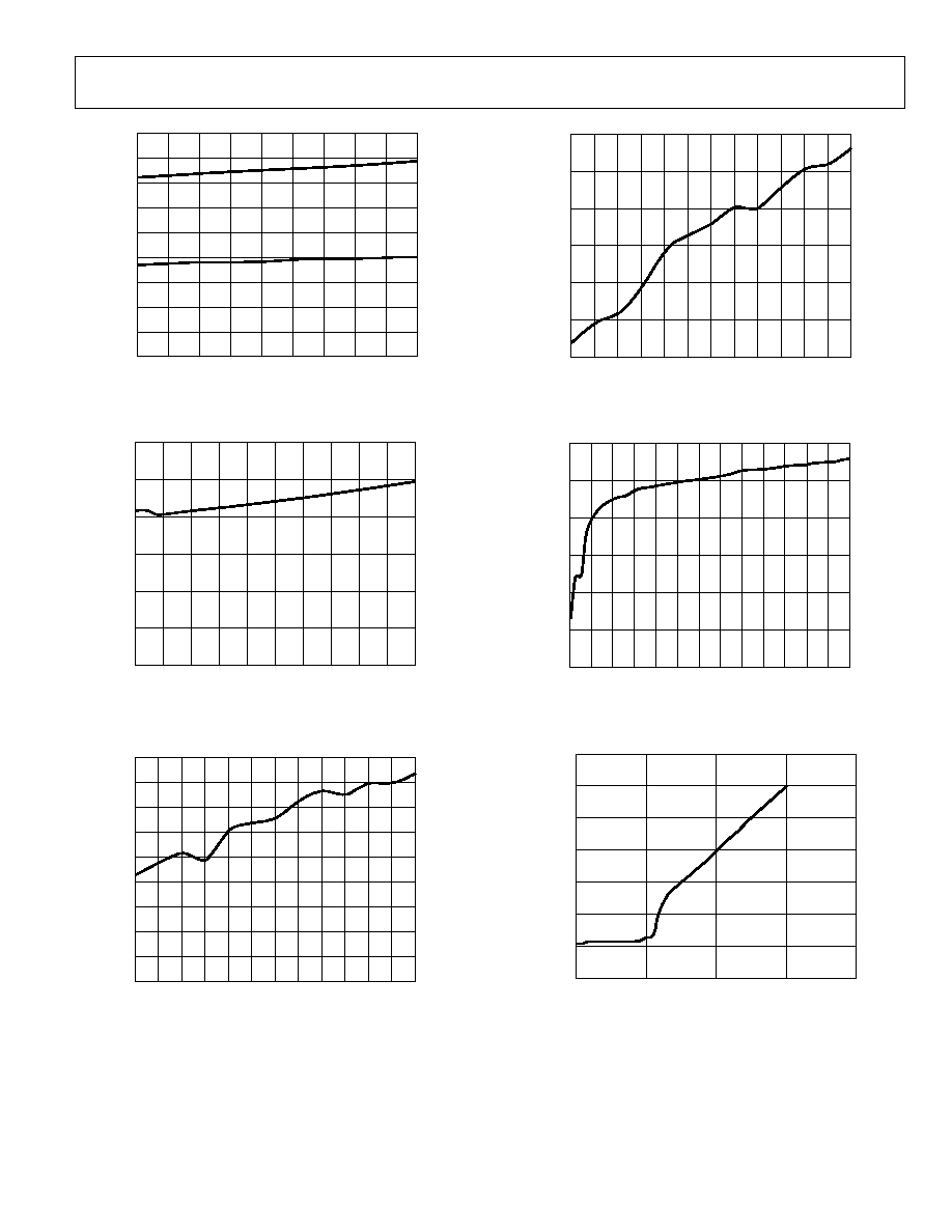
TYPICAL PERFORMANCE CHARACTERISTICS
LEAKAGE RESISTANCE (M
)
TE
MP
E
RATURE
E
RROR (
∞
C)
10
0
≠20
90
≠25
≠10
D+ TO V
CC
D+ TO GND
30
60
120
0
≠15
≠5
5
15
25
20
02657-A
-
004
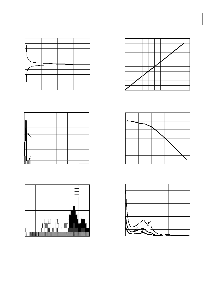
Figure 4. Temperature Error vs. PCB Track Resistance
FREQUENCY (MHz)
TE
MP
E
RATURE
E
RROR (∞C)
12
10
8
6
4
2
0
0
14
100mV
250mV
100
200
300
400
500
600
02657-A
-
005
Figure 5. Temperature Error vs. Power Supply Noise Frequency
FREQUENCY (MHz)
TE
MP
E
RATURE
E
RROR (∞C)
0
200
300
400
500
600
0
2
4
8
10
12
6
100
100mV
60mV
40mV
02657-A
-
006
Figure 6. Temperature Error vs. Common-Mode Noise Frequency
PIII TEMPERATURE (∞C)
RE
ADING (∞C)
0
10
20
30
40
50
60
70
80
90
100 110
0
10
20
30
40
50
60
70
80
90
100
110
02657-A
-
007
Figure 7. PentiumÆ III Temperature vs. ADM1026 Reading
CAPACITANCE (nF)
TE
MP
E
RATURE
E
RROR (
∞
C)
5
0
10
20
30
40
50
≠10
0
≠5
≠15
≠20
≠25
02657-A
-
008
Figure 8. Temperature Error vs. Capacitance Between D+ and D≠
FREQUENCY (MHz)
TE
MP
E
RATURE
E
RROR (∞C)
100
80
600
70
60
50
40
30
20
10
0
200
300
400
500
100mV
60mV
40mV
02657-A
-
009
Figure 9. Temperature Error vs. Differential-Mode Noise Frequency
ADM1026
Rev. A | Page 9 of 56
TEMPERATURE (∞C)
R
ESET TIM
E
OU
T (
m
s)
≠20
400
80
350
300
250
200
150
100
50
0
0
20
40
60
≠40
100
120
450
140
02657-A
-
010
Figure 10. Power-up Reset Timeout vs. Temperature
V
CC
(V)
I
DD
(mA)
3.0
2.5
2.0
1.5
1.0
0.5
3.00
4.00
3.25
3.50 3.75
4.25 4.50 4.75
5.25
5.00
0
5.50
02657-A
-
011
Figure 11. Supply Current vs. Supply Voltage
TEMPERATURE (∞C)
TE
MP
E
RATURE
E
RROR (∞C)
0.2
0
0.4
0.6
0.8
1.0
1.2
1.4
1.6
1.8
10
20
30
40
50
60
70
80
90 100 110 120
0
02657-A
-
012
Figure 12. Local Sensor Temperature Error
TEMPERATURE (∞C)
TE
MP
E
RATURE
E
RROR (∞C)
0
0.5
10
20
30
40
50
60
70
80
90 100 110 120
0
1.0
≠0.5
≠1.0
≠1.5
≠2.0
02657-A
-
013
Figure 13. Remote Sensor Temperature Error
TIME (s)
TE
MP
E
RATURE
(∞C)
4
2
0
20
40
60
80
100
120
0
6
8
10
12
14 16
18
20 22 24
26
02657-A
-
014
Figure 14. Response to Thermal Shock
0
0.5
1.0
2.5
3.0
1.5
2.0
3.5
0
1
2
3
4
V
BAT
VOLTAGE
V
BAT
ME
AS
URE
ME
NT
02657-A
-
015
Figure 15. V
BAT
Measurement vs. Voltage

ADM1026
Rev. A | Page 10 of 56
PRODUCT DESCRIPTION
The ADM1026 is a complete system hardware monitor for
microprocessor-based systems, providing measurement and
limit comparison of various system parameters. The ADM1026
has up to 19 analog measurement channels. Fifteen analog
voltage inputs are provided, five of which are dedicated to
monitoring +3.3 V, +5 V, and ±12 V power supplies, and the
processor core voltage. The ADM1026 can monitor two other
power supply voltages by measuring its own V
CC
and the main
system supply. One input (two pins) is dedicated to a remote
temperature-sensing diode. Two additional pins can be
configured as general-purpose analog inputs to measure
0 V to 2.5 V, or as a second temperature sensing input. The eight
remaining inputs are general-purpose analog inputs with a
range of 0 V to 2.5 V or 0 V to 3 V. The ADM1026 also has an
on-chip temperature sensor.
The ADM1026 has eight pins that can be configured for fan
speed measurement or as general-purpose logic I/O pins.
Another eight pins are dedicated to general-purpose logic I/O.
An additional pin can be configured as a general-purpose I/O
or as the bidirectional THERM pin.
Measured values can be read out via a 2-wire serial system
management bus, and values for limit comparisons can be
programmed over the same serial bus. The high speed,
successive approximation ADC allows frequent sampling of all
analog channels to ensure a fast interrupt response to any out-
of-limit measurement.
FUNCTIONAL DESCRIPTION
The ADM1026 is a complete system hardware monitor for
microprocessor-based systems. The device communicates with
the system via a serial system management bus. The serial bus
controller has a hardwired address line for device selection
(ADD, Pin 15), a serial data line for reading and writing
addresses and data (SDA, Pin 14), and an input line for the
serial clock (SCL, Pin 13). All control and programming
functions of the ADM1026 are performed over the serial bus.
Measurement Inputs
Programmability of the analog and digital measurement inputs
makes the ADM1026 extremely flexible and versatile. The
device has an 8-bit A/D converter, and 17 analog measurement
input pins that can be configured in different ways.
Pins 25 and 26 are dedicated temperature inputs and may be
connected to the cathode and anode of a remote temperature-
sensing diode.
Pins 27 and 28 may be configured as temperature inputs and
connected to a second temperature-sensing diode, or may be
reconfigured as analog inputs with a range of 0 V to 2.5 V.
Pins 29 to 33 are dedicated analog inputs with on-chip
attenuators configured to monitor V
BAT
, +5 V, -12 V, +12 V,
and the processor core voltage V
CCP
, respectively.
Pins 34 to 41 are general-purpose analog inputs with a range
of 0 V to 2.5 V or 0 V to 3 V. These are mainly intended for
monitoring SCSI termination voltages, but may be used for
other purposes.
The ADC also accepts input from an on-chip band gap
temperature sensor that monitors system ambient temperature.
In addition, the ADM1026 monitors the supply from which it is
powered, 3.3 V STBY, so there is no need for a separate pin to
monitor the power supply voltage.
The ADM1026 has eight pins that are general-purpose logic
I/O pins (Pins 1, 2, and 43 to 48), a pin that can be configured
as GPIO or as a bidirectional thermal interrupt (THERM) pin
(Pin 42), and eight pins that can be configured for fan speed
measurement or as general-purpose logic pins (Pins 3 to 6 and
Pins 9 to 12).
Sequential Measurement
When the ADM1026 monitoring sequence is started, it cycles
sequentially through the measurement of analog inputs and the
temperature sensor, while at the same time the fan speed inputs
are independently monitored. Measured values from these
inputs are stored in value registers. These can be read over the
serial bus, or can be compared with programmed limits stored
in the limit registers. The results of out-of-limit comparisons are
stored in the interrupt status registers. An out-of-limit event
generates an interrupt on the INT line (Pin 17).
Any or all of the interrupt status bits can be masked by
appropriate programming of the interrupt mask registers.
Chassis Intrusion
A chassis intrusion input (Pin 16) is provided to detect
unauthorized tampering with the equipment. This event is
latched in a battery-backed register bit.
Resets
The ADM1026 has two power-on reset outputs, RESETMAIN
and RESETSTBY, that are asserted when 3.3 V MAIN or 3.3 V
STBY fall below the reset threshold. These give a 180 ms reset
pulse at power-up. RESETMAIN also functions as an active-low
RESET input.
ADM1026
Rev. A | Page 11 of 56
Fan Speed Control Outputs
The ADM1026 has two outputs intended to control fan speed,
though they can also be used for other purposes. Pin 18 is an
open drain, pulse width modulated (PWM) output with a
programmable duty cycle and an output frequency of 75 Hz.
Pin 23 is connected to the output of an on-chip, 8-bit, digital-to-
analog converter with an output range of 0 V to 2.5 V.
Either or both of these outputs may be used to implement a
temperature-controlled fan by controlling the speed of a fan
using the temperature measured by the on-chip temperature
sensor or remote temperature sensors.
INTERNAL REGISTERS
Table 4 describes the principal registers of the ADM1026. For
more detailed information, see Table 11 to Table 124.
Table 4. Principal Registers
Type Description
Address Pointer
Contains the address that selects one of
the other internal registers. When writing
to the ADM1026, the first byte of data is
always a register address, and is written
to the address pointer register.
Configuration
Registers
Provide control and configuration for
various operating parameters.
Fan Divisor
Registers
Contain counter prescaler values for fan
speed measurement.
DAC/PWM
Control Registers
Contain speed values for PWM and DAC
fan drive outputs.
GPIO Configuration
Registers
Configure the GPIO pins as input or
output and for signal polarity.
Value and Limit
Registers
Store the results of analog voltage inputs,
temperature, and fan speed
measurements, along with their limit
values.
Status Registers
Store events from the various interrupt
sources.
Mask Registers
Allow masking of individual interrupt
sources.
EEPROM
The ADM1026 has 8 kB of nonvolatile, electrically erasable,
programmable read-only memory (EEPROM) from register
Addresses 8000h to 9FFFh. This may be used for permanent
storage of data that is not lost when the ADM1026 is powered
down, unlike the data in the volatile registers. Although referred
to as read-only memory, the EEPROM can be written to (as well
as read from) via the serial bus in exactly the same way as the
other registers. The main differences between the EEPROM and
other registers are
∑ An EEPROM location must be blank before it can be
written to. If it contains data, it must first be erased.
∑ Writing to EEPROM is slower than writing to RAM.
∑ Writing to the EEPROM should be restricted because its
typical cycle life is 100,000 write operations, due to the
usual EEPROM wear-out mechanisms.
The EEPROM in the ADM1026 has been qualified for two key
EEPROM memory characteristics: memory cycling endurance
and memory data retention.
Endurance qualifies the ability of the EEPROM to be cycled
through many program, read, and erase cycles. In real terms,
a single endurance cycle is composed of four independent,
sequential events, as follows:
1. Initial page erase sequence
2. Read/verify sequence
3. Program sequence
4. Second read/verify sequence
In reliability qualification, every byte is cycled from 00h to FFh
until a first fail is recorded, signifying the endurance limit of the
EEPROM memory.
Retention quantifies the ability of the memory to retain its
programmed data over time. The EEPROM in the ADM1026
has been qualified in accordance with the formal JEDEC
Retention Lifetime Specification (A117) at a specific junction
temperature (T
J
= 55∞C) to guarantee a minimum of 10 years
retention time. As part of this qualification procedure, the
EEPROM memory is cycled to its specified endurance limit
described above before data retention is characterized. This
means that the EEPROM memory is guaranteed to retain its
data for its full specified retention lifetime every time the
EEPROM is reprogrammed. Note that retention lifetime based
on an activation energy of 0.6 V derates with T
J
, as shown in
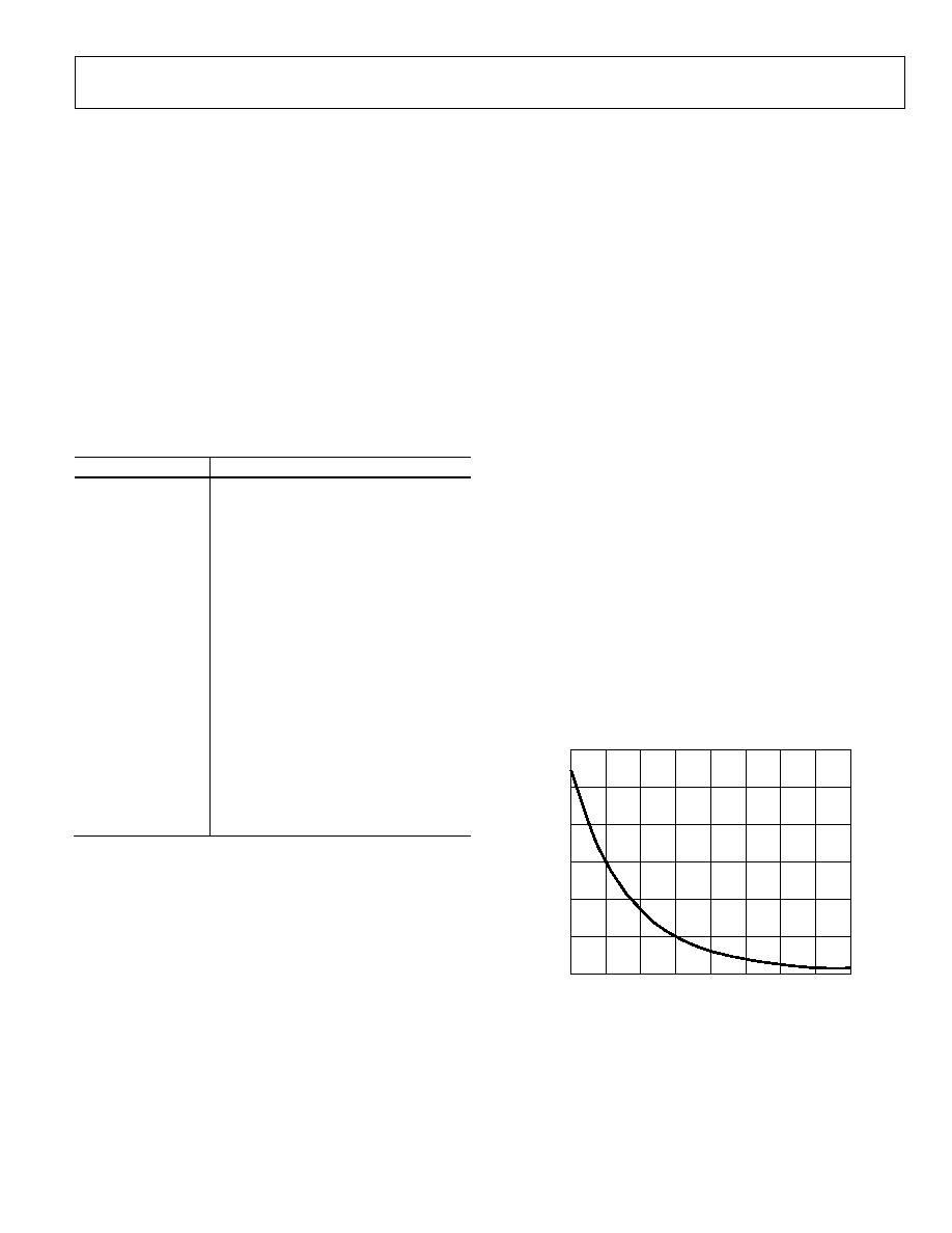
Figure 16.
JUNCTION TEMPERATURE (∞C)
250
RE
TE
NTION (Y
e
a
r
s
)
300
100
200
150
50
0
50
60
70
80
90
100
40
110
120
02657-A
-
016
Figure 16. Typical EEPROM Memory Retention

ADM1026
Rev. A | Page 12 of 56
Serial Bus Interface
Control of the ADM1026 is carried out via the serial system
management bus (SMBus). The ADM1026 is connected to this
bus as a slave device, under the control of a master device.
The ADM1026 has a 7-bit serial bus slave address. When the
device is powered on, it does so with a default serial bus address.
The 5 MSBs of the address are set to 01011, and the 2 LSBs are
determined by the logical states of Pin 15 ADD/NTESTOUT.
This pin is a three-state input that can be grounded, connected
to V
CC
, or left open-circuit to give three different addresses.
Table 5. Address Pin Truth Table
ADD Pin
A1
A0
GND
0
0
No Connect
1
0
V
CC
0
1
If ADD is left open-circuit, the default address is 0101110
(5Ch). ADD is sampled only at power-up on the first valid
SMBus transaction, so any changes made while the power is on
(and the address is locked) have no effect.
The facility to make hardwired changes to device addresses
allows the user to avoid conflicts with other devices sharing the
same serial bus, for example if more than one ADM1026 is used
in a system.
General SMBus Timing
Figure 17 and Figure 18 show timing diagrams for general read
and write operations using the SMBus. The SMBus specification
defines specific conditions for different types of read and write
operations, which are discussed later in this section.
The general SMBus protocol
1
operates as follows:
1. The master initiates data transfer by establishing a start
condition, defined as a high-to-low transition on the serial
data line (SDA) while the serial clock line SCL remains
high. This indicates that a data stream follows. All slave
peripherals connected to the serial bus respond to the start
condition and shift in the next 8 bits, consisting of a 7-bit
slave address (MSB first) and an R/W bit, which determine
the direction of the data transfer, that is, whether data is
written to or read from the slave device
(0 = write, 1 = read).
The peripheral whose address corresponds to the trans-
mitted address responds by pulling the data line low during
the low period before the ninth clock pulse, known as the
acknowledge bit, and holding it low during the high period
of this clock pulse. All other devices on the bus remain idle
while the selected device waits for data to be read from or
written to it. If the R/W bit is 0, the master writes to the
slave device. If the R/W bit is 1, the master reads from the
slave device.
2.
Data is sent over the serial bus in sequences of nine clock
pulses, 8 bits of data followed by an acknowledge bit from
the slave device. Data transitions on the data line must
occur during the low period of the clock signal and re-
main stable during the high period, because a low-to-high
transition when the clock is high may be interpreted as
a stop signal.
If the operation is a write operation, the first data byte after
the slave address is a command byte. This tells the slave
device what to expect next. It may be an instruction telling
the slave device to expect a block write, or it may simply be
a register address that tells the slave where subsequent data
is to be written.
Because data can flow in only one direction as defined by
the R/W bit, it is not possible to send a command to a slave
device during a read operation. Before doing a read oper-
ation, it may first be necessary to do a write operation to
tell the slave what type of read operation to expect and/or
the address from which data is to be read.
3. When all data bytes have been read or written, stop
conditions are established. In write mode, the master pulls
the data line high during the 10th clock pulse to assert a
stop condition. In read mode, the master
device releases the SDA line during the low period before
the ninth clock pulse, but the slave device does not pull
it low (called No Acknowledge). The master takes the data
line low during the low period before the 10th clock pulse,
then high during the 10th clock pulse to assert a stop
condition.
1
If it is required to perform several read or write operations in succession, the
master can send a repeat start condition instead of a stop condition to begin
a new operation.
ADM1026
Rev. A | Page 13 of 56
R/W
0
SCL
SDA
1
0
1
1
A1
A0
D7
D6
D5
D4
D3
D2
D1
D0
ACK. BY
SLAVE
START BY
MASTER
FRAME 1
SLAVE ADDRESS
FRAME 2
COMMAND CODE
1
9
1
ACK. BY
SLAVE
9
D7
D6
D5
D4
D3
D2
D1
D0
ACK. BY
SLAVE
STOP BY
MASTER
FRAME N
DATA BYTE
1
9
9
SCL
(CONTINUED)
SDA
(CONTINUED)
D7
D6
D5
D4
D3
D2
D1
D0
ACK. BY
SLAVE
FRAME 3
DATA BYTE
1
02657-A
-
017
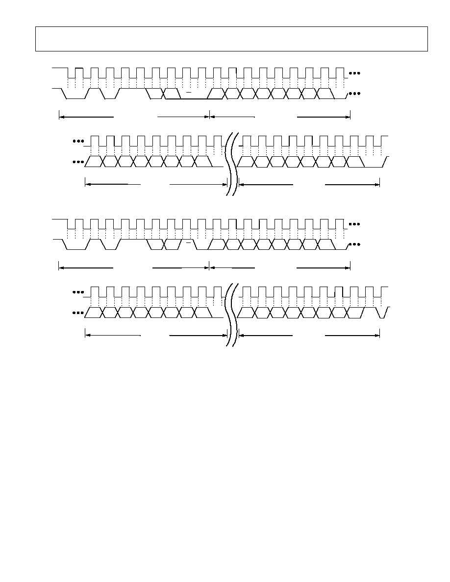
Figure 17. General SMBus Write Timing Diagram
R/W
0
SCL
SDA
1
0
1
1
A1
A0
D7
D6
D5
D4
D3
D2
D1
D0
ACK. BY
MASTER
START BY
MASTER
FRAME 1
SLAVE ADDRESS
FRAME 2
DATA BYTE
1
9
1
ACK. BY
SLAVE
9
D7
D6
D5
D4
D3
D2
D1
D0
NO ACK.
STOP BY
MASTER
FRAME N
DATA BYTE
1
9
9
SCL
(CONTINUED)
SDA
(CONTINUED)
D7
D6
D5
D4
D3
D2
D1
D0
ACK. BY
MASTER
FRAME 3
DATA BYTE
1
02657-A
-
018
Figure 18. General SMBus Read Timing Diagram
SMBus PROTOCOLS FOR RAM AND EEPROM
The ADM1026 contains volatile registers (RAM) and non-
volatile EEPROM. RAM occupies Addresses 00h to 6Fh, while
EEPROM occupies Addresses 8000h to 9FFFh.
Data can be written to and read from both RAM and EEPROM
as single data bytes and as block (sequential) read or write
operations of 32 data bytes, the maximum block size allowed by
the SMBus specification.
Data can only be written to unprogrammed EEPROM locations.
To write new data to a programmed location, it is first necessary
to erase it. EEPROM erasure cannot be done at the byte level;
the EEPROM is arranged as 128 pages of 64 bytes, and an entire
page must be erased. Note that of these 128 pages, only 124
pages are available to the user. The last four pages are reserved
for manufacturing purposes and cannot be erased/rewritten.
The EEPROM has three RAM registers associated with it,
EEPROM Registers 1, 2, and 3 at Addresses 06h, 0Ch, and 13h.
EEPROM Registers 1 and 2 are for factory use only. EEPROM
Register 3 sets up the EEPROM operating mode. Setting Bit 0 of
EEPROM Register 3 puts the EEPROM into read mode. Setting
Bit 1 puts it into programming mode. Setting Bit 2 puts it into
erase mode.
Only one of these bits must be set before the EEPROM may be
accessed. Setting no bits or more than one of them causes the
device to respond with No Acknowledge if an EEPROM read,
program, or erase operation is attempted.
It is important to distinguish between SMBus write opera-
tions, such as sending an address or command, and EEPROM
programming operations. It is possible to write an EEPROM
address over the SMBus, whatever the state of EEPROM
Register 3. However, EEPROM Register 3 must be correctly set
before a subsequent EEPROM operation can be performed. For
example, when reading from the EEPROM, Bit 0 of EEPROM
Register 3 can be set, even though SMBus write operations are
required to set up the EEPROM address for reading.

ADM1026
Rev. A | Page 14 of 56
Bit 3 of EEPROM Register 3 is used for EEPROM write protec-
tion. Setting this bit prevents accidental programming or era-
sure of the EEPROM. If an EEPROM write or erase operation
is attempted when this bit is set, the ADM1026 responds with
No Acknowledge. This bit is write-once and can only be cleared
by a power-on reset.
EEPROM Register 3 Bit 7 is used for clock extend. Program-
ming an EEPROM byte takes approximately 250 µs, which
would limit the SMBus clock for repeated or block write opera-
tions. Because EEPROM block read/write access is slow, it is
recommended that this clock extend bit typically be set to 1.
This allows the ADM1026 to pull SCL low and extend the
clock pulse when it cannot accept any more data.
ADM1026 SMBus Operations
The SMBus specification defines several protocols for different
types of read and write operations. The ones used in the
ADM1026 are discussed below. The following abbreviations are
used in the diagrams:
S Start
W Write
P Stop
A Acknowledge
R Read
A
No Acknowledge
ADM1026 Write Operations
Send Byte
In this operation, the master device sends a single command
byte to a slave device, as follows:
1. The master device asserts a start condition on the SDA.
2. The master sends the 7-bit slave address followed by the
write bit (low).
3. The addressed slave device asserts an ACK on the SDA.
4. The master sends a command code.
5. The slave asserts ACK on the SDA.
6. The master asserts a stop condition on the SDA and the
transaction ends.
In the ADM1026, the send byte protocol is used to write a
register address to RAM for a subsequent single-byte read from
the same address or block read or write starting at that address.
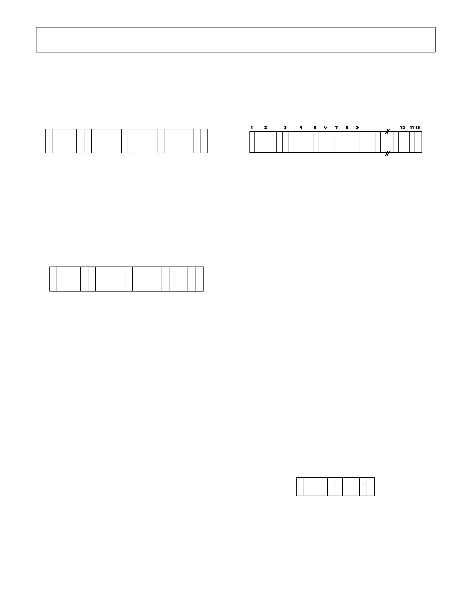
This is illustrated in Figure 19.
S
SLAVE
ADDRESS
W
RAM
ADDRESS
(00h TO 6Fh)
A
A
P
1
2
3
4
5
6
02657-A
-
019
Figure 19. Setting a RAM Address for Subsequent Read
If it is required to read data from the RAM immediately after
setting up the address, the master can assert a repeat start
condition immediately after the final ACK and carry out a
single byte read, block read, or block write operation without
asserting an intermediate stop condition.
Write Byte/Word
In this operation, the master device sends a command byte and
one or two data bytes to the slave device as follows:
1. The master device asserts a start condition on the SDA.
2. The master sends the 7-bit slave address followed by the
write bit (low).
3. The addressed slave device asserts an ACK on the SDA.
4. The master sends a command code.
5. The slave asserts an ACK on the SDA.
6. The master sends a data byte.
7. The slave asserts an ACK on the SDA.
8. The master sends a data byte (or may assert stop here.)
9. The slave asserts an ACK on the SDA.
10. The master asserts a stop condition on the SDA to end the
transaction.
In the ADM1026, the write byte/word protocol is used for four
purposes. The ADM1026 knows how to respond by the value of
the command byte and EEPROM Register 3.
The first purpose is to write a single byte of data to RAM. In
this case, the command byte is the RAM address from 00h to
6Fh and the (only) data byte is the actual data. This is illustrated
in Figure 20.
S
SLAVE
ADDRESS
W A
RAM
ADDRESS
(00h TO 6Fh)
1
2
3
4
5
6
A DATA A P
7 8
02657-A
-
020
Figure 20. Single Byte Write to RAM
The protocol is also used to set up a 2-byte EEPROM address
for a subsequent read or block read. In this case, the command
byte is the high byte of the EEPROM address from 80h to 9Fh.
The (only) data byte is the low byte of the EEPROM address.
This is illustrated in Figure 21.
S
SLAVE
ADDRESS
W
EEPROM
ADDRESS
HIGH BYTE
(80h TO 9Fh)
1
3
4
5
6
A
A
7
A
2
P
8
EEPROM
ADDRESS
LOW BYTE
(00h TO FFh)
02657-A
-
021
Figure 21. Setting an EEPROM Address
If it is required to read data from the EEPROM immediately
after setting up the address, the master can assert a repeat start
condition immediately after the final ACK and carry out a
single-byte read or block read operation without asserting an
intermediate stop condition. In this case, Bit 0 of EEPROM
Register 3 should be set.
The third use is to erase a page of EEPROM memory. EEPROM
memory can be written to only if it is previously erased. Before
writing to one or more EEPROM memory locations that are
already programmed, the page or pages containing those
locations must first be erased. EEPROM memory is erased by
writing an EEPROM page address plus an arbitrary byte of data
with Bit 2 of EEPROM Register 3 set to 1.
ADM1026
Rev. A | Page 15 of 56
Because the EEPROM consists of 128 pages of 64 bytes, the
EEPROM page address consists of the EEPROM address high
byte (from 80h to 9Fh) and the two MSBs of the low byte. The
lower six bits of the EEPROM address (low byte only) specify
addresses within a page and are ignored during an erase
operation.
S
SLAVE
ADDRESS
W A
EEPROM
ADDRESS
HIGH BYTE
(80h TO 9Fh)
1
2
3
4
5
6
A
A ARBITRARY
DATA
7
8
EEPROM
ADDRESS
LOW BYTE
(00h TO FFh)
A Y
9 10
02657-A
-022
Figure 22. EEPROM Page Erasure
Page erasure takes approximately 20 ms. If the EEPROM is
accessed before erasure is complete, the ADM1026 responds
with No Acknowledge.
Last, this protocol is used to write a single byte of data to
EEPROM. In this case, the command byte is the high byte of the
EEPROM address from 80h to 9Fh. The first data byte is the low
byte of the EEPROM address, and the second data byte is the
actual data. Bit 1 of EEPROM Register 3 must be set. This is
illustrated in Figure 23.
S
SLAVE
ADDRESS
W A
EEPROM
ADDRESS
HIGH BYTE
(80h TO 9Fh)
1
2
3
4
5
6
A
A DATA
7
8
EEPROM
ADDRESS
LOW BYTE
(00h TO FFh)
A Y
9 10
02657-A
-023
Figure 23. Single-Byte Write to EEPROM
Block Write
In this operation, the master device writes a block of data to a
slave device. The start address for a block write must have been
set previously. In the case of the ADM1026, this is done by a
Send Byte operation to set a RAM address or by a write
byte/word operation to set an EEPROM address.
1. The master device asserts a start condition on the SDA.
2. The master sends the 7-bit slave address followed by the
write bit (low).
3. The addressed slave device asserts an ACK on the SDA.
4. The master sends a command code that tells the slave
device to expect a block write. The ADM1026 command
code for a block write is A0h (10100000).
5. The slave asserts an ACK on the SDA.
6. The master sends a data byte (20h) that tells the slave
device that 32 data bytes are being sent to it. The master
should always send 32 data bytes to the ADM1026.
7. The slave asserts an ACK on the SDA.
8. The master sends 32 data bytes.
9. The slave asserts an ACK on the SDA after each data byte.
10. The master sends a packet error checking (PEC ) byte.
11. The ADM1026 checks the PEC byte and issues an ACK if
correct. If incorrect (NACK), the master resends the data
bytes.
12. The master asserts a stop condition on the SDA to end the
transaction.
S
SLAVE
ADDRESS
W A
COMMAND
A0h BLOCK
WRITE
A
A DATA 1
BYTE
COUNT
A
A
A P
DATA 2 A DATA
32
PEC
02857-
A-
024
Figure 24. Block Write to EEPROM or RAM
When performing a block write to EEPROM, Bit 1 of EEPROM
Register 3 must be set.
Unlike some EEPROM devices that limit block writes to within
a page boundary, there is no limitation on the start address
when performing a block write to EEPROM, except:
∑ There must be at least 32 locations from the start address
to the highest EEPROM address (9FFF) to avoid writing to
invalid addresses.
∑ If the addresses cross a page boundary, both pages must be
erased before programming.
ADM1026 Read Operations
The ADM1026 uses the SMBus read protocols described here.
Receive Byte
In this operation, the master device receives a single byte from a
slave device as follows:
1. The master device asserts a start condition on the SDA.
2. The master sends the 7-bit slave address followed by the
read bit (high).
3. The addressed slave device asserts an ACK on the SDA.
4. The master receives a data byte.
5. The master asserts a NO ACK on the SDA.
6. The master asserts a stop condition on the SDA to end the
transaction.
In the ADM1026, the receive byte protocol is used to read a
single byte of data from a RAM or EEPROM location whose
address has previously been set by a send byte or write
byte/word operation. Figure 25 shows this. When reading from
EEPROM, Bit 0 of EEPROM Register 3 must be set.
S
SLAVE
ADDRESS
R A DATA A P
1
2
3
4
5 6
02657-A
-
025
Figure 25. Single-Byte Read from EEPROM or RAM
ADM1026
Rev. A | Page 16 of 56
Block Read
In this operation, the master device reads a block of data from a
slave device. The start address for a block read must have been
set previously. In the case of the ADM1026 this is done by a
send byte operation to set a RAM address, or by a write
byte/word operation to set an EEPROM address. The block read
operation consists of a send byte operation that sends a block
read command to the slave, immediately followed by a repeated
start and a read operation that reads out multiple data bytes as
follows:
1. The master device asserts a start condition on the SDA.
2. The master sends the 7-bit slave address followed by the
write bit (low).
3. The addressed slave device asserts an ACK on the SDA.
4. The master sends a command code that tells the slave
device to expect a block read. The ADM1026 command
code for a block read is A1h (10100001).
5. The slave asserts an ACK on the SDA.
6. The master asserts a repeat start condition on the SDA.
7. The master sends the 7-bit slave address followed by the
read bit (high).
8. The slave asserts an ACK on the SDA.
9. The ADM1026 sends a byte count data byte that tells the
master how many data bytes to expect. The ADM1026
always returns 32 data bytes (20h), the maximum allowed
by the SMBus 1.1 specification.
10. The master asserts an ACK on the SDA.
11. The master receives 32 data bytes.
12. The master asserts an ACK on the SDA after each data byte.
13. The ADM1026 issues a PEC byte to the master. The master
should check the PEC byte and issue another block read if
the PEC byte is incorrect.
14. A NACK is generated after the PEC byte to signal the end
of the read.
15. The master asserts a stop condition on the SDA to end the
transaction.
S
SLAVE
ADDRESS
W A
COMMAND
A1h BLOCK
READ
A
S
R
A
P
DATA
32
PEC A
A BYTE
COUNT
A DATA 1 A
SLAVE
ADDRESS
02657-A
-
026
Figure 26. Block Read from EEPROM or RAM
When block reading from EEPROM, Bit 0 of EEPROM
Register 3 must be set.
Note that although the ADM1026 supports packet error
checking (PEC), its use is optional. The PEC byte is calculated
using CRC-8. The frame check sequence (FCS) conforms to
CRC-8 by the polynomial:
C(x) = x
8
+ x
2
+ x
1
+ 1
Consult the SMBus 1.1 Specification for more information.
MEASUREMENT INPUTS
The ADM1026 has 17 external analog measurement pins that
can be configured to perform various functions. It also meas-
ures two supply voltages, 3.3 V MAIN and 3.3 V STBY, and the
internal chip temperature.
Pins 25 and 26 are dedicated to remote temperature measure-
ment, while Pins 27 and 28 can be configured as analog inputs
with a range of 0 V to 2.5 V, or as inputs for a second remote
temperature sensor.
Pins 29 to 33 are dedicated to measuring V
BAT
, +5 V, -12 V,
+12 V supplies, and the processor core voltage V
CCP.
The
remaining analog inputs, Pins 34 to 41, are general-purpose
analog inputs with a range of 0 V to 2.5 V (Pins 34 and 35) or
0 V to 3 V (Pins 36 to 41).
A-to-D Converter (ADC)
These inputs are multiplexed into the on-chip, successive
approximation, analog-to-digital converter. The ADC has a
resolution of 8 bits. The basic input range is 0 V to 2.5 V, which
is the input range of A
IN6
to A
IN9
, but five of the inputs have
built-in attenuators to allow measurement of V
BAT
, +5 V, -12 V,
+12 V, and the processor core voltage V
CCP
, without any external
components. To allow the tolerance of these supply voltages, the
ADC produces an output of 3/4 full scale (decimal 192) for the
nominal input voltage, and so has adequate headroom to cope
with over voltages. Table 6 shows the input ranges of the analog
inputs and output codes of the ADC.
When the ADC is running, it samples and converts an analog
or local temperature input every 711 µs (typical value). Each
input is measured 16 times and the measurements are averaged
to reduce noise, so the total conversion time for each input is
11.38 ms.
Measurements on the remote temperature (D1 and D2) inputs
take 2.13 ms. These are also measured 16 times and are
averaged, so the total conversion time for a remote temperature
input is 34.13 ms.

ADM1026
Rev. A | Page 17 of 56
Table 6. A-to-D Output Code vs. V
IN
Input Voltage
A-to-D Output
+12 V
IN
≠12
V
IN
+5
V
IN
3.3 V MAIN
3.3 V STBY
V
BAT
1
V
CCP
A
IN (0≠5)
A
IN (6≠9)
Decimal
Binary
< 0.0625
< -15.928
< 0.026
< 0.0172
NA
< 0.012
< 0.012
< 0.010
0
00000000
0.062-0.125
-15.928-15.855
0.026-0.052
0.017-0.034
NA
0.012-0.023
0.012-0.023
0.010-0.019
1
00000001
0.125-0.187
-15.855-15.783
0.052-0.078
0.034-0.052
NA
0.023-0.035
0.023-0.035
0.019-0.029
2
00000010
0.188-0.250
-15.783-15.711
0.078-0.104
0.052-0.069
NA
0.035-0.047
0.035-0.047
0.029-0.039
3
00000011
0.250-0.313
-15.711-15.639
0.104-0.130
0.069-0.086
NA
0.047-0.058
0.047-0.058
0.039-0.049
4
00000100
0.313-0.375
-15.639-15.566
0.130-0.156
0.086-0.103
NA
0.058-0.070
0.058-0.070
0.049-0.058
5
00000101
0.375-0.438
-15.566-15.494
0.156-0.182
0.103-0.120
NA
0.070-0.082
0.070-0.082
0.058-0.068
6
00000110
0.438-0.500
-15.494-15.422
0.182-0.208
0.120-0.138
NA
0.082-0.094
0.082-0.094
0.068-0.078
7
00000111
0.500-0.563
-15.422-15.349
0.208-0.234
0.138-0.155
NA
0.094-0.105
0.094-0.105
0.078-0.087
8
00001000
∑
∑
∑
4.000-4.063
-11.375-11.303
1.667-1.693
1.110-1.127
NA
0.750-0.780
0.750-0.780
0.625-0.635
64
(1/4 scale)
01000000
∑
∑
∑
8.000-8.063
-6.750-6.678
3.333-3.359
2.000-2.016
2.000-2.016
1.500-1.512
1.500-1.512
1.250-1.260
128
(1/2 scale)
10000000
∑
∑
∑
12.000-12.063
-2.125-2.053
5-5.026
3.330-3.347
3.000-3.016
2.250-2.262
2.250-2.262
1.875-1.885
192
(3/4 scale)
11000000
∑
∑
∑
15.313-15.375
1.705-1.777
6.38-6.406
4.249-4.267
3.828-3.844
2.871-2.883
2.871-2.883
2.392-2.402
245
11110101
15.375-15.437
1.777-1.850
6.406-6.432
4.267-4.284
3.844-3.860
2.883-2.895
2.883-2.895
2.402-2.412
246
11110110
15.437-15.500
1.850-1.922
6.432-6.458
4.284-4.301
3.860-3.875
2.895-2.906
2.895-2.906
2.412-2.422
247
11110111
15.500-15.563
1.922-1.994
6.458-6.484
4.301-4.319
3.875-3.890
2.906-2.918
2.906-2.918
2.422-2.431
248
11111000
15.562-15.625
1.994-2.066
6.484-6.51
4.319-4.336
3.890-3.906
2.918-2.930
2.918-2.930
2.431-2.441
249
11111001
15.625-15.688
2.066-2.139
6.51-6.536
4.336-4.353
3.906-3.921
2.930-2.941
2.930-2.941
2.441-2.451
250
11111010
15.688-15.750
2.139-2.211
6.536-6.563
4.353-4.371
3.921-3.937
2.941-2.953
2.941-2.953
2.451-2.460
251
11111011
15.750-15.812
2.211-2.283
6.563-6.589
4.371-4.388
3.937-3.953
2.953-2.965
2.953-2.965
2.460-2.470
252
11111100
15.812-15.875
2.283-2.355
6.589-6.615
4.388-4.405
3.953-3.969
2.965-2.977
2.965-2.977
2.470-2.480
253
11111101
15.875-15.938
2.355-2.428
6.615-6.641
4.405-4.423
3.969-3.984
2.977-2.988
2.977-2.988
2.480-2.490
254
11111110
>15.938
>2.428
>6.634 >4.423 >3.984 >2.988 >2.988 >2.490 255
11111111
1
V
BAT
is not accurate for voltages under 1.5 V (see Figure 15).
ADM1026
Rev. A | Page 18 of 56
Voltage Measurement Inputs
The internal structure for all the analog inputs is shown in
Figure 27. Each input circuit consists of an input protection
diode, an attenuator, plus a capacitor to form a first-order low-
pass filter that gives each voltage measurement input immunity
to high frequency noise. The -12 V input also has a resistor
connected to the on-chip reference to offset the negative voltage
range so that it is always positive and can be handled by the
ADC. This allows most popular power supply voltages to be
monitored directly by the ADM1026 without requiring any
additional resistor scaling.
109.4k
18.5pF
21.9k
+V
CCP
9.3pF
V
REF
17.5k
114.3k
≠12V
49.5k
82.7k
4.5pF
V
BAT
* SEE TEXT
A
IN0
≠ A
IN5
(0V ≠ 3V)
109.4k
4.6pF
21.9k
A
IN6
≠ A
IN9
(0V ≠ 2.5V)
4.6pF
52.5k
50k
4.6pF
83.5k
+5V
21k
9.3pF
113.5k
+12V
MUX
02657-A
-
027
Figure 27. Voltage Measurement Inputs
Setting Other Input Ranges
A
IN0
to A
IN9
can easily be scaled to voltages other than 2.5 V or
3 V. If the input voltage range is zero to some positive voltage, all
that is required is an input attenuator, as shown in Figure 28.
R1
R2
V
IN
A
IN(0≠9)
02657-A
-
028
Figure 28. Scaling A
IN0
- A
IN9
However, when scaling A
IN0
to A
IN5
, it should be noted that
these inputs already have an on-chip attenuator, because their
primary function is to monitor SCSI termination voltages. This
attenuator loads any external attenuator. The input resistance of
the on-chip attenuator can be between 100 k and 200 k. For
this tolerance not to affect the accuracy, the output resistance
of the external attenuator should be very much lower than
this, that is, 1 k in order to add not more than 1% to the
total unadjusted error (TUE). Alternatively, the input can be
buffered using an op amp.
(
)
(
)
IN5
IN0
fs
A
A
V
R2
R1
to
for
0
.
3
0
.
3
-
=
(
)
(
)
IN9
IN6
fs
A
A
V
R2
R1
to
for
5
.
2
5
.
2
-
=
Negative and bipolar input ranges can be accommodated by
using a positive reference voltage to offset the input voltage
range so that it is always positive. To monitor a negative input
voltage, an attenuator can be used as shown in Figure 29.
R1
R2
V
IN
A
IN(0≠9)
02657-A
-
029
Figure 29. Scaling and Offsetting A
IN0
- A
IN9
for Negative Inputs
This offsets the negative voltage so that the ADC always sees a
positive voltage. R1 and R2 are chosen so that the ADC input
voltage is zero when the negative input voltage is at its
maximum (most negative) value, that is:
OS
fs
V
V
R2
R1
-
=
This is a simple and low cost solution, but note the following:
∑ Because the input signal is offset but not inverted, the input
range is transposed. An increase in the magnitude of the
negative voltage (going more negative) causes the input
voltage to fall and give a lower output code from the ADC.
Conversely, a decrease in the magnitude of the negative
voltage causes the ADC code to increase. The maximum
negative voltage corresponds to zero output from the ADC.
This means that the upper and lower limits are transposed.
∑ For the ADC output to be full scale when the negative
voltage is zero, V
OS
must be greater than the full-scale
voltage of the ADC, because V
OS
is attenuated by R1 and
R2. If V
OS
is equal to or less than the full-scale voltage of
the ADC, the input range is bipolar but not necessarily
symmetrical.
This is a problem only if the ADC output must be full scale
when the negative voltage is zero.
ADM1026
Rev. A | Page 19 of 56
Symmetrical bipolar input ranges can be accommodated easily
by making V
OS
equal to the full-scale voltage of the analog input,
and by adding a third resistor to set the positive full scale.
R1
R2
V
IN
A
IN(0≠9)
R3
+V
OS
02657-A
-
030
Figure 30. Scaling and Offsetting A
IN0
- A
IN9
for Bipolar Inputs
OS
fs
V
V
R2
R1
-
=
Note that R3 has no effect as the input voltage at the device pin
is zero when V
IN
= negative full scale.
(
)
(
)
IN5
IN0
fs
A
A
V
R3
R1
to
for
0
.
3
0
.
3
-
=
(
)
(
)
IN9
IN6
fs
A
A
V
R3
R1
to
for
5
.
2
5
.
2
-
=
Also, note that R2 has no effect as the input voltage at the device
pin is equal to V
OS
when V
IN
= positive full scale.
Battery Measurement Input (V
BAT
)
The V
BAT
input allows the condition of a CMOS backup battery
to be monitored. This is typically a lithium coin cell such as a
CR2032. The V
BAT
input is accurate only for voltages greater
than 1.5 V (see Figure 15). Typically, the battery in a system is
required to keep some device powered on when the system is in
a powered-off state. The V
BAT
measurement input is specially
designed to minimize battery drain. To reduce current drain
from the battery, the lower resistor of the V
BAT
attenuator is not
connected, except whenever a V
BAT
measurement is being made.
The total current drain on the V
BAT
pin is 80 nA typical (for a
maximum V
BAT
voltage = 4 V), so a CR2032 CMOS battery
functions in a system in excess of the expected 10 years. Note
that when a V
BAT
measurement is not being made, the current
drain is reduced to 6 nA typical. Under normal voltage meas-
urement operating conditions, all measurements are made in a
round-robin format, and each reading is actually the result of
16 digitally averaged measurements. However, averaging is not
carried out on the V
BAT
measurement to reduce measurement
time and therefore reduce the current drain from the battery.
The V
BAT
current drain when a measurement is being made is
calculated by
PERIOD
PULSE
BAT
T
T
V
I
◊
=
k
100
For example, when V
BAT
= 3 V,
A
n
78
ms
273
711
k
100
V
3
=
µ
◊
=
s
I
where T
PULSE
= V
BAT
measurement time (711 µs typical),
T
PERIOD
= time to measure all analog inputs (273 ms typical),
and V
BAT
input battery protection.
V
BAT
Input Battery Protection
In addition to minimizing battery current drain, the V
BAT
measurement circuitry was specifically designed with battery
protection in mind. Internal circuitry prevents the battery from
being back-biased by the ADM1026 supply or through any
other path under normal operating conditions. In the unlikely
event of a catastrophic ADM1026 failure, the ADM1026
includes a second level of battery protection including a series
3 k resistor to limit current to the battery, as recommended by
UL. Thus, it is not necessary to add a series resistor between the
battery and the V
BAT
input; the battery can be connected directly
to the V
BAT
input to improve voltage measurement accuracy.
ADC
V
BAT
DIGITAL
CONTROL
49.5k
82.7k
4.5pF
3k
3k
02657-A
-
031
Figure 31. Equivalent V
BAT
Input Protection Circuit
Reference Output (V
REF
)
The ADM1026 offers an on-chip reference voltage (Pin 24) that
can be used to provide a 1.82 V or 2.5 V reference voltage out-
put. This output is buffered and specified to sink or source a
load current of 2 mA. The reference voltage outputs 1.82 V if
Bit 2 of Configuration Register 3 (Address 07h) is 0; it outputs
2.5 V when this bit is set to 1. This voltage reference output can
be used to provide a stable reference voltage to external cir-
cuitry such as LDOs. The load regulation of the V
REF
output is
typically 0.15% for a sink current of 2 mA and 0.15% for 2 mA
source current. There may be some ripple present on the V
REF
output that requires filtering (±4 m V
MAX
). Figure 32 shows the
recommended circuitry for the V
REF
output for loads less than
2 mA. For loads in excess of 2 mA, external circuitry, such as
that shown in Figure 33, can be used to buffer the V
REF
output.
10k
0.1
µ
F
V
REF
ADM1026
24
V
REF
02657-A
-
033
Figure 32. V
REF
Interface Circuit for V
REF
Loads < 2 mA
ADM1026
Rev. A | Page 20 of 56
If the V
REF
output is not being used, it should be left uncon-
nected. Do not connect V
REF
to GND using a capacitor. The
internal output buffer on the voltage reference is capacitively
loaded, which can cause the voltage reference to oscillate. This
affects temperature readings reported back by the ADM1026.
The recommended interface circuit for the V
REF
output is shown
in Figure 33.
10k
0.1
µ
F
ADM1026
24
+12V
0.1
µ
F
10
µ
F
50
V
REF
NDT3055
V
REF
02657-A
-
034
Figure 33. V
REF
Interface Circuit for V
REF
Loads > 2 mA
TEMPERATURE MEASUREMENT SYSTEM
Local Temperature Measurement
The ADM1026 contains an on-chip band gap temperature
sensor whose output is digitized by the on-chip ADC. The
temperature data is stored in the local temperature value
register (Address 1Fh). As both positive and negative temper-
atures can be measured, the temperature data is stored in twos
complement format, as shown in Table 7. Theoretically, the
temperature sensor and ADC can measure temperatures from
-128∞C to +127∞C with a resolution of 1∞C. Temperatures below
T
MIN
and above T
MAX
are outside the operating temperature
range of the device, however, so local temperature measure-
ments outside this range are not possible. Temperature
measurement from -128∞C to +127∞C is possible using a
remote sensor.
Remote Temperature Measurement
The ADM1026 can measure the temperature of two remote
diode sensors, or diode-connected transistors, connected to
Pins 25 and 26, or 27 and 28.
Pins 25 and 26 are a dedicated temperature input channel.
Pins 27 and 28 can be configured to measure a diode sensor by
clearing Bit 3 of Configuration Register 1 (Address 00h) to 0.
If this bit is 1, then Pins 27 and 28 are A
IN8
and A
IN9
.
The forward voltage of a diode or diode-connected transistor,
operated at a constant current, exhibits a negative temperature
coefficient of about -2 mV/∞C. Unfortunately, the absolute
value of V
be
varies from device to device, and individual
calibration is required to null this out, so the technique is
unsuitable for mass production.
The technique used in the ADM1026 is to measure the change
in V
be
when the device is operated at two different currents,
given by
( )
N
n
q
T
K
V
be
log
◊
◊
=
where K is Boltzmann's constant, q is the charge on the carrier,
T is the absolute temperature in Kelvins, and N is the ratio of
the two currents.
Figure 34 shows the input signal conditioning used to measure
the output of a remote temperature sensor. This figure shows
the external sensor as a substrate transistor provided for
temperature monitoring on some microprocessors, but it could
equally well be a discrete transistor such as a 2N3904.
If a discrete transistor is used, the collector is not grounded
and should be linked to the base. If a PNP transistor is used,
the base is connected to the D- input and the emitter to the
D+ input. If an NPN transistor is used, the emitter is connected
to the D- input and the base to the D+ input.
To prevent ground noise from interfering with the measure-
ment, the more negative terminal of the sensor is not referenced
to ground but is biased above ground by an internal diode at the
D- input.
To measure V
be
, the sensor is switched between operating
currents of I and N ◊ I. The resulting waveform is passed
through a 65 kHz low-pass filter to remove noise, and to a
chopper-stabilized amplifier that performs the functions of
amplification and rectification of the waveform to produce a
DC voltage proportional to V
be
. This voltage is measured
by the ADC to give a temperature output in 8-bit, twos
complement format. To further reduce the effects of noise,
digital filtering is performed by averaging the results of 16
measurement cycles. A remote temperature measurement
takes nominally 2.14 ms.
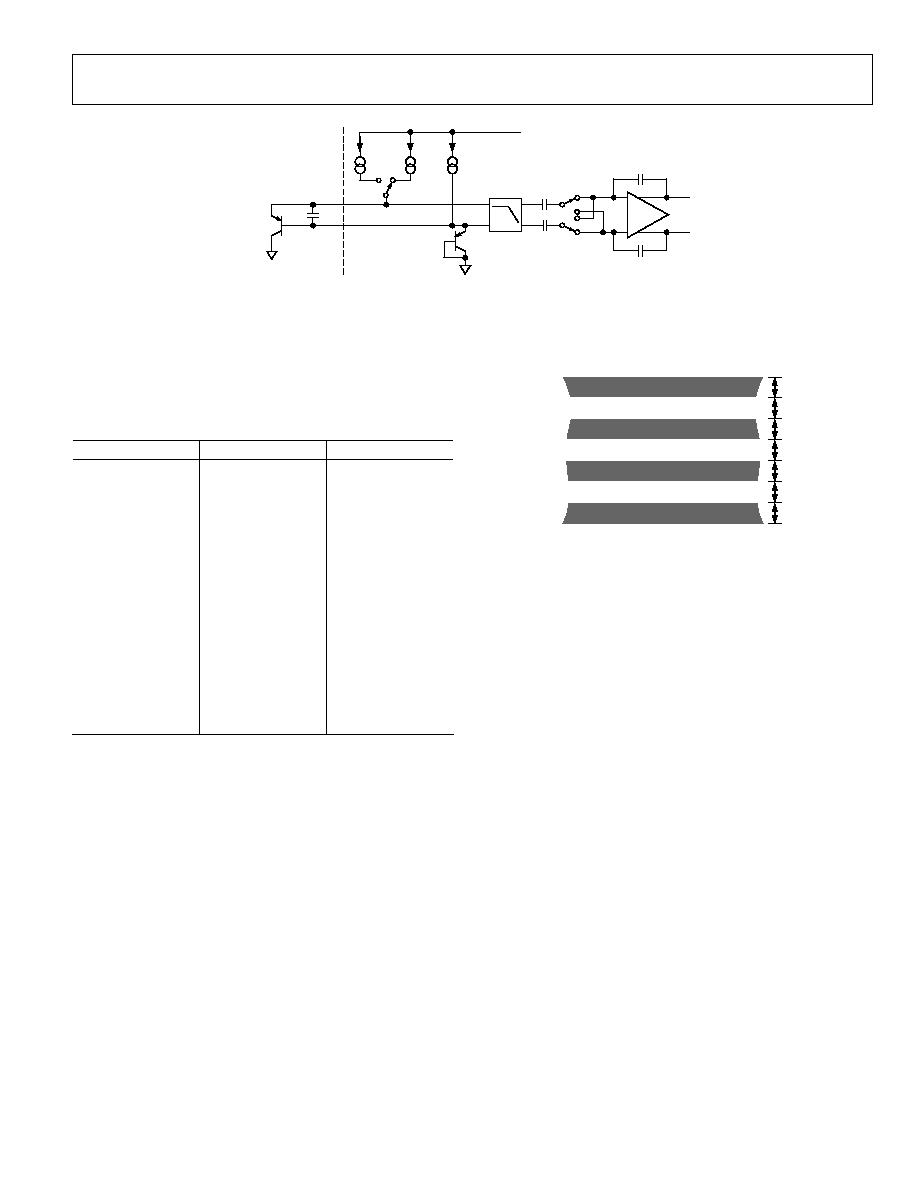
ADM1026
Rev. A | Page 21 of 56
C1*
D+
D≠
REMOTE
SENSING
TRANSISTOR
I
N
◊
I
I
BIAS
V
DD
V
OUT+
TO ADC
V
OUT≠
BIAS
DIODE
LOW-PASS FILTER
f
C
= 65kHz
CAPACITOR C1 IS OPTIONAL. IT IS ONLY NECESSARY IN NOISY ENVIRONMENTS.
C1 = 2.2nF TYPICAL, 3nF MAX.
*
02657-A
-032
Figure 34. Signal Conditioning for Remote Diode Temperature Sensors
The results of external temperature measurements are stored in
8-bit, twos complement format, as illustrated in Table 7.
Table 7. Temperature Data Format
Temperature
Digital Output
Hex
-128∞C
1000 0000
80
-125∞C
1000 0011
83
-100∞C
1001 1100
9C
-75∞C
1011 0101
B5
-50∞C
1100 1110
CE
-25∞C
1110 0111
E7
-10∞C
11110110
F6
0∞C
0000 0000
00
10∞C
0000 1010
0A
25∞C
0001 1001
19
50∞C
0011 0010
32
75∞C
0100 1011
4B
100∞C
0110 0100
64
125∞C
0111 1101
7D
127∞C
0111 1111
7F
Layout Considerations
Digital boards can be electrically noisy environments. Take
these precautions to protect the analog inputs from noise,
particularly when measuring the very small voltages from a
remote diode sensor.
∑ Place the ADM1026 as close as possible to the remote
sensing diode. Provided that the worst noise sources such
as clock generators, data/address buses, and CRTs are
avoided, this distance can be 4 to 8 inches.
∑ Route the D+ and D- tracks close together, in parallel, with
grounded guard tracks on each side. Provide a ground
plane under the tracks if possible.
∑ Use wide tracks to minimize inductance and reduce noise
pickup. A 10 mil track minimum width and spacing is
recommended.
10MIL
10MIL
10MIL
10MIL
10MIL
10MIL
10MIL
GND
D+
GND
D≠
02657-A
-
035
Figure 35. Arrangement of Signal Tracks
∑ Try to minimize the number of copper/solder joints, which
can cause thermocouple effects. Where copper/solder
joints are used, make sure that they are in both the D+ and
D- paths and are at the same temperature.
∑ Thermocouple effects should not be a major problem
because 1∞C corresponds to about 240 µV, and
thermocouple voltages are about 3 µV/∞C of temperature
difference. Unless there are two thermocouples with a big
temperature differential between them, thermocouple
voltages should be much less than 200 mV.
∑ Place a 0.1 µF bypass capacitor close to the ADM1026.
∑ If the distance to the remote sensor is more than eight
inches, the use of twisted-pair cable is recommended.
This works from about 6 to 12 feet.
∑ For very long distances (up to 100 feet), use shielded
twisted pair such as Belden #8451 microphone cable.
Connect the twisted pair to D+ and D- and the shield to
GND close to the ADM1026. Leave the remote end of the
shield unconnected to avoid ground loops.
Because the measurement technique uses switched current
sources, excessive cable and/or filter capacitance can affect the
measurement. When using long cables, the filter capacitor may
be reduced or removed. Cable resistance can also introduce
errors. A 1 series resistance introduces about 0.5∞C error.

ADM1026
Rev. A | Page 22 of 56
Limit Values
Limit values for analog measurements are stored in the appropri
ate limit registers. In the case of voltage measurements, high and
low limits can be stored so that an interrupt request is generated
if the measured value goes above or below acceptable values. In
the case of temperature, a hot temperature or high limit can be
programmed, and a hot temperature hysteresis or low limit can
be programmed, which is usually some degrees lower. This can
be useful because it allows the system to be shut down when the
hot limit is exceeded, and restarted automatically when it has
cooled down to a safe temperature.
Analog Monitoring Cycle Time
The analog monitoring cycle begins when a 1 is written to the
start bit (Bit 0), and a 0 to the INT_Clear bit (Bit 2) of the con-
figuration register. INT_Enable (Bit 1) should be set to 1 to
enable the INToutput. The ADC measures each analog input in
turn, starting with Remote Temperature Channel 1 and ending
with local temperature. As each measurement is completed, the
result is automatically stored in the appropriate value register.
This round-robin monitoring cycle continues until it is disabled
by writing a 0 to Bit 0 of the configuration register. Because the
ADC is typically left to free-run in this way, the most recently
measured value of any input can be read out at any time.
For applications where the monitoring cycle time is important,
it can easily be calculated.
The total number of channels measured is
∑ Five dedicated supply voltage inputs
∑ Ten general-purpose analog inputs
∑ 3.3 V MAIN
∑ 3.3 V STBY
∑ Local temperature
∑ Two remote temperature
Pins 28 and 27 are measured both as analog inputs A
IN8
/A
IN9
and
as remote temperature input D2+/D2-, irrespective of which
configuration is selected for these pins.
If Pins 28 and 27 are configured as A
IN8
/A
IN9
, the measurements
for these channels are stored in Registers 27h and 29h, and the
invalid temperature measurement is discarded. On the other
hand, if Pins 28 and 27 are configured as D2+/D2-, the temper-
ature measurement is stored in Register 29h, and there is no
valid result in Register 27h.
As mentioned previously, the ADC performs a conversion every
711 µs on the analog and local temperature inputs and every
2.13 ms on the remote temperature inputs. Each input is
measured 16 times and averaged to reduce noise.
The total monitoring cycle time for voltage and temperature
inputs is therefore nominally
(18 ◊ 16 ◊ 0.711) + (2 ◊ 16 ◊ 2.13) = 273 ms
The ADC uses the internal 22.5 kHz clock, which has a toler-
ance of ±6%, so the worst-case monitoring cycle time is 290 ms.
The fan speed measurement uses a completely separate
monitoring loop, as described later.
Input Safety
Scaling of the analog inputs is performed on-chip, so external
attenuators are typically not required. However, because the
power supply voltages appear directly at the pins, it is advisable
to add small external resistors (that is, 500 ) in series with the
supply traces to the chip to prevent damaging the traces or
power supplies should an accidental short such as a probe
connect two power supplies together.
Because the resistors form part of the input attenuators, they
affect the accuracy of the analog measurement if their value
is too high. The worst such accident would be connecting
-12 V to +12 V where there is a total of 24 V difference. With
the series resistors, this would draw a maximum current of
approximately 24 mA.
ANALOG OUTPUT
The ADM1026 has a single analog output from an unsigned
8-bit DAC that produces 0 V to 2.5 V (independent of the refer-
ence voltage setting). The input data for this DAC is contained
in the DAC control register (Address 04h). The DAC control
register defaults to FFh during a power-on reset, which pro-
duces maximum fan speed. The analog output may be amplified
and buffered with external circuitry such as an op amp and a
transistor to provide fan speed control. During automatic fan
speed control, described later, the four MSBs of this register set
the minimum fan speed.
Suitable fan drive circuits are shown in Figure 36 through
Figure 40. When using any of these circuits, note the following:
∑ All of these circuits provide an output range from 0 V to
almost +12 V, apart from Figure 36, which loses the base-
emitter voltage drop of Q1 due to the emitter-follower
configuration.
∑ To amplify the 2.5 V range of the analog output up to 12 V,
the gain of these circuits needs to be about 4.8.
∑ Take care when choosing the op amp to ensure that its
input common-mode range and output voltage swing are
suitable.
∑ The op amp may be powered from the +12 V rail alone
or from ±12 V. If it is powered from +12 V, the input
common-mode range should include ground to accom-
modate the minimum output voltage of the DAC, and the
output voltage should swing below 0.6 V to ensure that the
transistor can be turned fully off.
∑ If the op amp is powered from -12 V, precautions such as
a clamp diode to ground may be needed to prevent the
base-emitter junction of the output transistor being
reverse-biased in the unlikely event that the output of
the op amp should swing negative for any reason.
ADM1026
Rev. A | Page 23 of 56
∑ In all these circuits, the output transistor must have an
I
CMAX
greater than the maximum fan current, and be
capable of dissipating power due to the voltage dropped
across it when the fan is not operating at full speed.
∑ If the fan motor produces a large back EMF when switched
off, it may be necessary to add clamp diodes to protect the
output transistors in the event that the output goes from
full scale to zero very quickly.
Q1
2N2219A
DAC
R1
10k
1/4
LM324
R2
36k
12V
02657-A
-
036
Figure 36. Fan Drive Circuit with Op Amp and Emitter-Follower
Q1
BD136
2SA968
DAC
R1
10k
1/4
LM324
R2
39k
R4
1k
R3
1k
12V
02657-A
-
037
Figure 37. Fan Drive Circuit with Op Amp and PNP Transistor
Q1
IRF9620
DAC
12V
R1
10k
1/4
LM324
R2
39k
R3
100k
02657-A
-
038
Figure 38. Fan Drive Circuit with Op Amp and P-Channel MOSFET
R2
100k
Q1/Q2
MBT3904
DUAL
12V
DAC
R3
39k
R4
10k
Q3
IRF9620
R2
100k
02657-A
-
039
Figure 39. Discrete Fan Drive Circuit with P-Channel MOSFET, Single Supply
R2
100k
Q1/Q2
MBT3904
DUAL
+12V
DAC
R3
39k
R4
10k
R1
4.7k
≠12V
Q3
IRF9620
02657-A
-
040
Figure 40. Discrete Fan Drive Circuit with P-Channel MOSFET, Dual Supply
PWM Output
Fan speed may also be controlled using pulse width modulation
(PWM). The PWM output (Pin 18) produces a pulsed output
with a frequency of approximately 75 Hz and a duty cycle
defined by the contents of the PWM control register (Address
05h). During automatic fan speed control, described below, the
four MSBs of this register set the minimum fan speed.
The open drain PWM output must be amplified and buffered
to drive the fans. The PWM output is intended to be used with
an NMOS driver, but may be inverted by setting Bit 1 of Test
Register 1 (Address 14h) if using PMOS drivers. Figure 41
shows how a fan may be driven under PWM control using an
N-channel MOSFET.
+V
Q1
NDT3055L
PWM
3.3V
10k
TYP
5V OR 12V
FAN
02657-A
-
041
Figure 41. PWM Fan Drive Circuit Using an N-Channel MOSFET
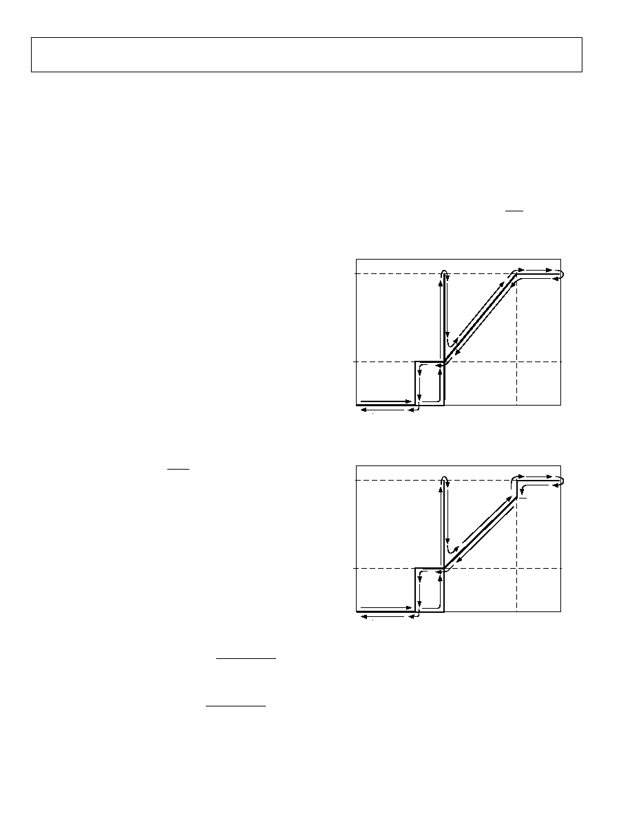
ADM1026
Rev. A | Page 24 of 56
Automatic Fan Speed Control
The ADM1026 offers a simple method of controlling fan speed
according to temperature without intervention from the host
processor. Monitoring must be enabled by setting Bit 0 of
Configuration Register 1 (Address 00h), to enable automatic fan
speed control. Automatic fan speed control can be applied to the
DAC output, the PWM output, or both, by setting Bit 5 and/or
Bit 6 of Configuration Register 1.
The T
MIN
registers (Addresses 10h to 12h) contain minimum
temperature values for the three temperature channels (on-chip
sensor and two remote diodes). This is the temperature at which
a fan starts to operate when the temperature sensed by the
controlling sensor exceeds T
MIN
. T
MIN
can be the same or
different for all three channels. T
MIN
is set by writing a twos
complement temperature value to the T
MIN
registers. If any
sensor channel is not required for automatic fan speed control,
T
MIN
for that channel should be set to 127∞C (01111111).
In automatic fan speed control mode, (as shown Figure 42 and
Figure 43) the four MSBs of the DAC control register (Address
04h) and PWM control register (Address 05h) set the minimum
values for the DAC and PWM outputs. Note that, if both DAC
control and PWM control are enabled (Bits 5 and 6 of
Configuration Register 1 = 1), the four MSBs of the DAC
control register (Address 04h) define the minimum fan speed
values for both the DAC and PWM outputs. The value in the
PWM control register (Address 05h) has no effect.
Minimum DAC Code DAC
MIN
= 16 ◊ D
256
5
.
2
Code
Voltage
Output
DAC
◊
=
Minimum PWM Duty Cycle PWMMIN = 6.67 ◊ D
where D is the decimal equivalent of Bits 7 to 4 of the register.
When the temperature measured by any of the sensors exceeds
the corresponding T
MIN
, the fan is spun up for 2 seconds with
the fan drive set to maximum (full scale from the DAC or 100%
PWM duty cycle). The fan speed is then set to the minimum as
previously defined. As the temperature increases, the fan drive
increases until the temperature reaches T
MIN
+ 20∞C.
The fan drive at any temperature up to 20∞C above T
MIN
is
given by
(
)
20
100
MIN
ACTUAL
MIN
MIN
T
T
PWM
PWM
PWM
-
◊
-
+
=
or
(
)
20
240
MIN
ACTUAL
MIN
MIN
T
T
DAC
DAC
DAC
-
◊
-
+
=
For simplicity of the automatic fan speed algorithm, the DAC
code increases linearly up to 240, not its full scale of 255.
However, when the temperature exceeds T
MIN
+20∞C, the DAC
output jumps to full scale. To ensure that the maximum cooling
capacity is always available, the fan drive is always set by the
sensor channel demanding the highest fan speed.
If the temperature falls, the fan does not turn off until the
temperature measured by all three temperature sensors has
fallen to their corresponding T
MIN
- 4∞C. This prevents the fan
from cycling on and off continuously when the temperature is
close to T
MIN
.
Whenever a fan starts or stops during automatic fan speed
control, a one-off interrupt is generated at the INT output. This
is described in more detail in the section on the ADM1026
Interrupt Structure.
PWM
OUTPUT
MIN
TEMPERATURE
T
MIN
SPIN UP FOR 2 SECONDS
100%
T
MIN
≠ 4∞C
T
MIN
+ 20∞C
02657-A
-
042
Figure 42. Automatic PWM Fan Control Transfer Function
DAC
OUTPUT
MIN
TEMPERATURE
T
MIN
255
T
MIN
≠ 4∞C
T
MIN
+ 20∞C
SPIN UP FOR 2 SECONDS
240
02657-A
-
043
Figure 43. Automatic DAC Fan Control Transfer Function
Fan Inputs
Pins 3 to 6 and 9 to 12 may be configured as fan speed
measuring inputs by clearing the corresponding bit(s) of
Configuration Register 2 (Address 01h), or as general-purpose
logic inputs/outputs by setting bits in this register. The power-
on default value for this register is 00h, which means all the
inputs are set for fan speed measurement.
ADM1026
Rev. A | Page 25 of 56
Signal conditioning in the ADM1026 accommodates the slow
rise and fall times typical of fan tachometer outputs. The fan
tach inputs have internal 10 k pull-up resistors to 3.3 V STBY.
In the event that these inputs are supplied from fan outputs that
exceed the supply, either resistive attenuation of the fan signal
or diode clamping must be included to keep inputs within an
acceptable range. Figure 44 through Figure 47 show circuits for
common fan tach outputs.
If the fan tach output is open-drain or has a resistive pull-up to
V
CC
, then it can be connected directly to the fan input, as shown
in Figure 44.
12V
FAN SPEED
COUNTER
FAN(0≠7)
PULL-UP
4.7k
TYP
TACH
OUTPUT
V
CC
02657-A
-
044
Figure 44. Fan with Tach Pull-Up to +V
CC
If the fan output has a resistive pull-up to +12 V (or other
voltage greater than 3.3 V STBY), the fan output can be clamped
with a Zener diode, as shown in Figure 45. The Zener voltage
should be chosen so that it is greater than V
IH
but less than 3.3 V
STBY, allowing for the voltage tolerance of the Zener.
12V
FAN SPEED
COUNTER
FAN(0≠7)
PULL-UP
4.7k
TYP
TACH
OUTPUT
V
CC
* CHOOSE ZD1 VOLTAGE APPROXIMATELY 0.8
◊
V
CC
ZD1*
ZENER
02657-A
-
045
Figure 45. Fan with Tach Pull-Up to Voltage > V
CC
(e.g. 12 V),
Clamped with Zener Diode
If the fan has a strong pull-up (less than 1 k) to +12 V, or a
totem pole output, a series resistor can be added to limit the
Zener current, as shown in Figure 46. Alternatively, a resistive
attenuator may be used, as shown in Figure 47.
R1 and R2 should be chosen such that
(
)
STBY
V
3
.
3
PULLUP
V
2V
<
+
+
◊
<
R2
R1
PULLUP
R
R2
12V
FAN SPEED
COUNTER
FAN(0≠7)
PULL-UP TYP
<1 k
OR
TOTEM POLE
TACH
OUTPUT
V
CC
* CHOOSE ZD1 VOLTAGE APPROXIMATELY 0.8
◊
V
CC
ZD1*
ZENER
R1
10k
02657-A
-
046
Figure 46. Fan with Strong Tach Pull-Up to > V
CC
or Totem Pole Output,
Clamped with Zener and Resistor
12V
FAN SPEED
COUNTER
FAN(0≠7)
<1 k
TACH
OUTPUT
V
CC
R1*
* SEE TEXT
02657-A
-
047
Figure 47. Fan with Strong Tach Pull-Up to >V
CC
or Totem Pole Output,
Attenuated with R1/R2
FAN SPEED MEASUREMENT
The fan counter does not count the fan tach output pulses
directly because the fan speed may be less than 1000 RPM and
it would take several seconds to accumulate a reasonably large
and accurate count. Instead, the period of the fan revolution is
measured by gating an on-chip 22.5 kHz oscillator into the
input of an 8-bit counter for two periods of the fan tach output,
as shown in Figure 48, so the accumulated count is actually
proportional to the fan tach period and inversely proportional
to the fan speed.
22.5kHz
CLOCK
CONFIGURATION
REG. 1 BIT 0
FAN0
INPUT
FAN0
MEASUREMENT
PERIOD
FAN1
MEASUREMENT
PERIOD
START OF
MONITORING
CYCLE
FAN1
INPUT
1
2
3
4
1
2
3
4
02657-A-048
Figure 48. Fan Speed Measurement
The monitoring cycle begins when a 1 is written to the monitor
bit (Bit 0 of Configuration Register 1). The INT_Enable (Bit 1)
should be set to 1 to enable the INT output.

ADM1026
Rev. A | Page 26 of 56
The fan speed counter starts counting as soon as the fan
channel has been switched to. If the fan tach count reaches 0xFF,
the fan has failed or is not connected. If a fan is connected and
running, the counter is reset on the second tach rising edge, and
oscillator pulses are actually counted from the second rising
tach edge to the fourth rising edge. The measurement then
switches to the next fan channel. Here again, the counter begins
counting and is reset on the second tach rising edge, and
oscillator pulses are counted from the second rising edge to the
fourth rising edge. This is repeated for the other six fan
channels.
Note that fan speed measurement does not occur until 1.8
seconds after the monitor bit has been set. This is to allow the
fans adequate time to spin up. Otherwise, the ADM1026 could
generate false fan failure interrupts. During the 1.8 second fan
spin-up time, all fan tach registers read 0x00.
To accommodate fans of different speed and/or different
numbers of output pulses per revolution, a prescaler (divisor) of
1, 2, 4, or 8 may be added before the counter. Divisor values for
Fans 0 to 3 are contained in the Fan 0≠3 divisor register
(Address 02h) and those for Fans 4 to 7 in the Fan 4≠7 divisor
register (Address 03h). The default value is 2, which gives a
count of 153 for a fan running at 4400 RPM producing two
output pulses per revolution. The count is calculated by the
equation:
Divisor
RPM
Count
◊
◊
◊
=
60
10
5
.
22
3
For constant-speed fans, fan failure is typically considered to
have occurred when the speed drops below 70% of nominal,
corresponding to a count of 219. Full scale (255) is reached if
the fan speed fell to 60% of its nominal value. For temperature-
controlled, variable-speed fans, the situation is different.
Table 8 shows the relationship between fan speed and time per
revolution at 60%, 70%, and 100% of nominal RPM for fan
speeds of 1100, 2200, 4400, and 8800 RPM, and the divisor that
would be used for each of these fans, based on two tach pulses
per revolution.
Limit Values
Fans generally do not over-speed if run from the correct
voltage, so the failure condition of interest is under speed due to
electrical or mechanical failure. For this reason, only low speed
limits are programmed into the limit registers for the fans. It
should be noted that because fan period rather than speed is
being measured, a fan failure interrupt occurs when the
measurement exceeds the limit value.
Fan Monitoring Cycle Time
The fan speeds are measured in sequence from 0 to 7. The
monitoring cycle time depends on the fan speed, the number
of tach output pulses per revolution, and the number of fans
being monitored.
If a fan is stopped or running so slowly that the fan speed
counter reaches 255 before the second tach pulse after initializa-
tion, or before the fourth tach pulse during measurement, the
measurement is terminated. This also occurs if an input is con-
figured as GPIO instead of fan. Any channels connected in this
manner time out after 255 clock pulses.
The worst-case measurement time for a fan-configured channel
occurs when the counter reaches 254 from start to the second
tach pulse and reaches 255 after the second tach pulse. Taking
into account the tolerance of the oscillator frequency, the worst-
case measurement time is
509 ◊ D ◊ 0.05 ms
where:
509 is the total number of clock pulses.
D is the divisor: 1, 2, 4, or 8.
0.05 ms is the worst-case oscillator period in ms.
The worst-case fan monitoring cycle time is the sum of the
worst-case measurement time for each fan.
Although the fan monitoring cycle and the analog input
monitoring cycle are started together, they are not synchronized
in any other way.
Table 8. Fan Speeds and Divisors
Time
Per
Divisor RPM
Nominal Rev
RPM (ms)
70% RPM
Rev 70% (ms)
60% RPM
Rev 60% (ms)
˜ 1
8800
6.82
6160
9.74
5280
11.36
˜ 2
4400
13.64
3080
19.48
2640
22.73
˜ 4
2200
27.27
1540
38.96
1320
45.45
˜ 8
1100
54.54
770
77.92
660
90.9
ADM1026
Rev. A | Page 27 of 56
Chassis Intrusion Input
The chassis intrusion input is an active high input intended for
detection and signaling of unauthorized tampering with the
system. When this input goes high, the event is latched in Bit 6
of Status Register 4, and an interrupt is generated. The bit
remains set until cleared by writing a 1 to CI clear, Bit 1 of
Configuration Register 3 (05h), as long as battery voltage is
connected to the V
BAT
input. The CI clear bit itself is cleared by
writing a 0 to it.
The CI input detects chassis intrusion events even when the
ADM1026 is powered off (provided battery voltage is applied to
V
BAT
) but does not immediately generate an interrupt. Once a
chassis intrusion event is detected and latched, an interrupt is
generated when the system is powered on.
The actual detection of chassis intrusion is performed by an
external circuit that detects, for example, when the cover has
been removed. A wide variety of techniques may be used for the
detection, for example:
∑ A microswitch that opens or closes when the cover is
removed.
∑ A reed switch operated by magnet fixed to the cover.
∑ A hall-effect switch operated by magnet fixed to the cover.
∑ A phototransistor that detects light when the cover is
removed.
The chassis intrusion input can also be used for other types of
alarm input. Figure 49 shows a temperature alarm circuit using
an AD22105 temperature switch sensor. This produces a low-
going output when the preset temperature is exceeded, so the
output is inverted by Q1 to make it compatible with the CI
input. Q1 can be almost any small-signal NPN transistor, or a
TTL or CMOS inverter gate may be used if one is available.
See the AD22105 data sheet on the Analog Devices, Inc.
website (www.analog.com) for information on selecting R
SET
.
V
CC
R
SET
AD22105
TEMPERATURE
SENSOR
6
CI
R1
10k
Q1
7
3
2
1
18
02657-A
-
049
Figure 49. Using the CI Input with a Temperature Sensor
General-Purpose I/O Pins (Open Drain)
The ADM1026 has eight pins that are dedicated to general-
purpose logic input/output (Pins 1, 2, and 43 to 48), eight pins
that can be configured as general-purpose logic pins or fan
speed inputs (Pins 3 to 6, and 9 to 12), and one pin that can
be configured as GPIO16 or the bidirectional THERM pin
(Pin 42). The GPIO/FAN pins are configured as general-
purpose logic pins by setting Bits 0 to 7 of Configuration
Register 2 (Address 01h). Pin 42 is configured as GPIO16 by
setting Bit 0 of Configuration Register 3, or as the THERM
function by clearing this bit.
Each GPIO pin has four data bits associated with it, two bits in
one of the GPIO configuration registers (Addresses 08h to 0Bh),
one in the GPIO status registers (Addresses 24h and 25h), and
one in the GPIO mask registers (Addresses 1Ch and 1Dh)
Setting a direction bit = 1 in one of the GPIO configuration
registers makes the corresponding GPIO pin an output.
Clearing the direction bit to 0 makes it an input.
Setting a polarity bit = 1 in one of the GPIO configuration
registers makes the corresponding GPIO pin active high.
Clearing the polarity bit to 0 makes it active low.
When a GPIO pin is configured as an input, the corresponding
bit in one of the GPIO status registers is read-only, and is set
when the input is asserted ("asserted" may be high or low
depending on the setting of the polarity bit).
When a GPIO pin is configured as an output, the corresponding
bit in one of the GPIO status registers becomes read/write.
Setting this bit then asserts the GPIO output. (Here again,
"asserted" may be high or low depending on the setting of the
polarity bit.)
The effect of a GPIO status register bit on the INT output can
be masked out by setting the corresponding bit in one of the
GPIO mask registers. When the pin is configured as an output,
this bit is automatically masked to prevent the data written to
the status bit from causing an interrupt, with the exception of
GPIO16, which must be masked manually by setting Bit 7 of
Mask Register 4 (Reg 1Bh).
When configured as inputs, the GPIO pins may be connected to
external interrupt sources such as temperature sensors with
digital output. Another application of the GPIO pins would be
to monitor a processor's voltage ID code (VID code).

ADM1026
Rev. A | Page 28 of 56
ADM1026 Interrupt Structure
The Interrupt Structure of the ADM1026 is shown in Figure 53.
Interrupts can come from a number of sources, which are com-
bined to form a common INT output. When INT is asserted,
this output pulls low. The INT pin has an internal, 100 k
pull-up resistor.
Analog/Temperature Inputs
As each analog measurement value is obtained and stored in the
appropriate value register, the value and the limits from the
corresponding limit registers are fed to the high and low limit
comparators. The device performs greater than comparisons to
the high limits. An out-of-limit is also generated if a result is
less than or equal to a low limit. The result of each comparison
(1 = out of limit, 0 = in limit) is routed to the corresponding
bit input of Interrupt Status Register 1, 2, or 4 via a data
demultiplexer, and used to set that bit high or low as appro-
priate. Status bits are self-clearing. If a bit in a status register is
set due to an out-of-limit measurement, it continues to cause
INT to be asserted as long as it remains set, as described later.
However, if a subsequent measurement is in limit, it is reset and
does not cause INT to be reasserted. Status bits are unaffected
by clearing the interrupt.
Interrupt Mask Registers 1, 2, and 4 have bits corresponding to
each of the interrupt status register bits. Setting an interrupt
mask bit high conceals an asserted status bit from display on
Interrupt Pin 17. Setting an interrupt mask bit low allows the
corresponding status bit to be asserted and displayed on Pin 17.
After mask gating, the status bits are all OR'ed together to
produce the analog and fan interrupt that is used to set a latch.
The output of this latch is OR'ed with other interrupt sources to
produce the INT output. This pulls low if any unmasked status
bit goes high, that is, when any measured value goes out of limit.
When an INT output caused by an out-of-limit analog/
temperature measurement is cleared by one of the methods
described later, the latch is reset. It is not set again, and INT is
not reasserted until after two local temperature measure-ments
have been taken, even if the status bit remains set or a new
analog/temperature event occurs, as shown in Figure 50. This
delay corresponds to almost two monitoring cycles, and is about
530 ms. However, interrupts from other sources such as a fan or
GPIO can still occur. This is illustrated in Figure 51.
START OF ANALOG
MONITORING
CYCLE
OUT-OF-LIMIT
MEASUREMENT
START OF ANALOG
MONITORING
CYCLE
INT
INT CLEARED
LOCAL
TEMPERATURE
MEASUREMENT
START OF ANALOG
MONITORING
CYCLE
INT RE-ASSERTED
OUT-OF-LIMIT
MEASUREMENT
FULL MONITORING CYCLE = 273ms
TEMPERATURE
LOCAL
MEASUREMENT
02657-A
-
051
Figure 50. Delay After Clearing INT Before Reassertion
START OF ANALOG
MONITORING CYCLE
OUT-OF-LIMIT
MEASUREMENT
LOCAL TEMPEREATURE
MEASUREMENT
START OF ANALOG
MONITORING CYCLE
LOCAL TEMPERATURE
MEASUREMENT
START OF ANALOG
MONITORING CYCLE
INT
CLEARED
INT RE-ASSERTED
NEW INT
FROM FAN
NEW
INT
FROM GPIO
GPIO DE-ASSERTED
INT
INT
CLEARED
02657-A
-
052
Figure 51. Other Interrupt Sources Can Reassert INT Immediately

ADM1026
Rev. A | Page 29 of 56
Status Register 4 also stores inputs from two other interrupt
sources that operate in a different way from the other status bits.
If automatic fan speed control (AFC) is enabled, Bit 4 of Status
Register 4 is set whenever a fan starts or stops. This bit causes a
one-off INT output as shown in Figure 52. It is cleared during
the next monitoring cycle and if INT has been cleared, it does
not cause INT to be reasserted.
INT
INT CLEARED BY STATUS REGULAR 1 READ, BIT 2
OF CONFIGURATION REGULAR 1 SET, OR ARA
FAN ON
FAN OFF
02657-A
-
053
Figure 52. Assertion of INT Due to AFC Event
In a similar way, a change of state at the THERM output
(described in more detail later), sets Bit 3 of Status
Register 4 and causes a one-off INT output. A change of state at
the THERM output also causes Bit 0 of Status Register 1, Bit 1
of Status Register 1, or Bit 0 of Status Register 4 to be set,
depending on which temperature channel caused the THERM
event. This bit is reset during the next monitoring cycle,
provided the temperature channel is within the normal high
and low limits.
Fan Inputs
Fan inputs generate interrupts in a similar way to analog/
temperature inputs, but as the analog/ temperature inputs and
fan inputs have different monitoring cycles, they have separate
interrupt circuits. As the speed of each fan is measured, the
output of the fan speed counter is stored in a value register. The
result is compared to the fan speed limit and is used to set or
clear a bit in Status Register 3. In this case, the fan is monitored
only for under-speed (fan counter > fan speed limit). Mask
Register 3 is used to mask fan interrupts. After mask gating, the
fan status bits are OR'ed together and used to set a latch, whose
output is OR'ed with other interrupt sources to produce the INT
output.
Like the analog/temp interrupt, an INT output caused by an
out-of-limit fan speed measurement, once cleared, is not
reasserted until the end of the next monitoring cycle, although
other interrupt sources may cause INT to be asserted.
GPIO and CI Pins. When GPIO pins are configured as inputs,
asserting a GPIO input (high or low, depending on polarity) sets
the corresponding GPIO status bit in Status Registers 5 and 6, or
Bit 7 of Status Register 4 (GPIO16). A chassis intrusion event
sets Bit 6 of Status Register 4.
The GPIO and CI status bits, after mask gating, are OR'ed
together and OR'ed with other interrupt sources to produce the
INT output. GPIO and CI interrupts are not latched and cannot
be cleared by normal interrupt clearing. They can only be
cleared by masking the status bits or by removing the source of
the interrupt.
ENABLING AND CLEARING INTERRUPTS
The INT output is enabled when Bit 1 of Configuration
Register 1 (INT_Enable) is high, and Bit 2 (INT_Clear) is low.
INT may be cleared if
∑ Status Register 1 is read. Ideally, if polling the status
registers trying to identify interrupt sources, Status
Register 1 should be polled last, because a read of Status
Register 1 clears all the other interrupt status registers.
∑ The ADM1026 receives the alert response address (ARA)
(0001 100) over the SMBus.
∑ Bit 2 of Configuration Register 1 is set.
Bidirectional THERM Pin
The ADM1026 has a second interrupt pin (GPIO16/THERM
Pin 42) that responds only to critical thermal events. The
THERM pin goes low whenever a THERM limit is exceeded.
This function is useful for CPU throttling or system shutdown.
In addition, whenever THERM is activated, the PWM and DAC
outputs go full scale to provide fail-safe system cooling. This
output is enabled by setting Bit 4 of Configuration Register 1
(Register 00h). Whenever a THERM limit is exceeded, Bit 3 of
Status Register 4 (Reg 23h) is set, even if the THERM function
is disabled (Bit 4 of Configuration Register 1 = 0). In this case,
the THERM status bit is set, but the PWM and DAC outputs are
not forced to full scale.
Three thermal limit registers are provided for the three
temperature sensors at Addresses 0Dh to 0Fh. These registers
are dedicated to the THERM function and none of the other
limit registers have any effect on the THERM output.
If any of the temperature measurements exceed the correspond-
ing limit, THERM is asserted (low) and the DAC and PWM
outputs go to maximum to drive any cooling fans to full speed.
To avoid cooling fans cycling on and off continually when the
temperature is close to the limit, a fixed hysteresis of 5∞C is
provided. THERM is only deasserted when the measured
temperature of all three sensors is 5∞C below the limit.
Whenever the THERM output changes, INT is asserted, as
shown in Figure 54. However, this is edge-triggered, so if INT
is subsequently cleared by one of the methods previously
described, it is not reasserted, even if THERM remains asserted.
THERM causes INT to be reasserted only when it changes state.
ADM1026
Rev. A | Page 30 of 56
1 = OUT
OF LIMIT
HIGH AND LOW LIMIT
COMP
ARATORS
INT ENABLE
INT CLEAR
INT
INT TEMP
V
BAT
A
IN8
THERM
AFC
RESERVED
CI
GPIO16
EXT1 TEMP
EXT 2 TEMP
3.3V STBY
3.3V MAIN
+5V
V
CCP
+12V
≠12V
FAN0
FAN1
FAN2
FAN3
FAN4
FAN5
FAN6
FAN7
FROM FAN SPEED
VALUE AND
LIMIT REGISTERS
HIGH LIM
I
T
COMP
ARATOR
DATA
D
E
M
U
LTIPLEXER
1 = OUT
OF LIMIT
VALUE
HIGH LIMIT
GPIO0 TO GPIO7
GPIO8 TO GPIO15
MASKING DATA
FROM SMBus
MASKING DATA
FROM SMBus
A
IN0
A
IN1
A
IN2
A
IN3
A
IN4
A
IN5
A
IN6
A
IN7
HIGH LIMIT
LOW LIMIT
VALUE
FROM ANALOG/TEMP
VALUE AND LIMIT
REGISTERS
DATA
D
E
M
U
LTIPLEXER
MASK GATING
◊
8
STATUS
BIT
MASK
BIT
MASK DATA FROM
SMBus (SAME BIT
NAMES AND ORDER
AS STATUS BITS)
LATCH
RESET
IN OUT
CI
GPIO16
MASK GATING
◊
8
STATUS
BIT
MASK
BIT
MASK GATING
◊
8
STATUS
BIT
MASK
BIT
MASK GATING
◊
8
STATUS
BIT
MASK
BIT
MASK GATING
◊
8
STATUS
BIT
MASK
BIT
MASK GATING
◊
8
STATUS
BIT
MASK
BIT
MASK
REGISTER
1
S
T
ATUS
REGISTER
1
0
1
2
3
4
5
6
7
MASK
REGISTER
2
S
T
ATUS
REGISTER
2
0
1
2
3
4
5
6
7
MASK
REGISTER
4
S
T
ATUS
REGISTER
4
0
1
2
3
4
5
6
7
MASK
REGISTER
3
S
T
ATUS
REGISTER
3
0
1
2
3
4
5
6
7
MASK DATA FROM
SMBus (SAME BIT
NAMES AND ORDER
AS STATUS BITS)
MASK DATA FROM
SMBus (SAME BIT
NAMES AND ORDER
AS STATUS BITS)
MASK DATA FROM
SMBus (SAME BIT
NAMES AND ORDER
AS STATUS BITS)
LATCH
RESET
IN OUT
MASK REGISTER 5
MASK REGISTER 6
STATUS REGISTER 6
STATUS REGISTER 5
02657-A
-
050
Figure 53. Interrupt Structure
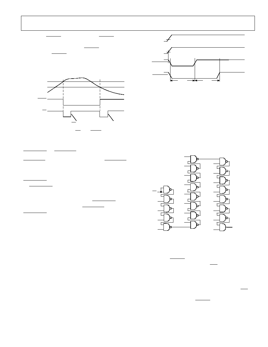
ADM1026
Rev. A | Page 31 of 56
Note that the THERM pin is bidirectional, so THERM may be
pulled low externally as an input. This causes the PWM and
DAC outputs to go to full scale until THERM is returned high
again. To disable THERM as an input, set Bit 0 of Configuration
Register 3 (Reg. 07h). This configures Pin 42 as GPIO16 and
prevents a low on Pin 42 from driving the fans at full speed.
THERM LIMIT
THERM LIMIT ≠ 5∞C
THERM
INT
INT CLEARED BY STATUS REG 1 READ,
BIT 2 OF CONFIG. REG. 1 SET, OR ARA
TEMPERATURE
02657-A-054
Figure 54. Assertion of INT Due to THERM Event
Reset Input and Outputs
The ADM1026 has two active low, power-on reset outputs,
RESETMAIN and RESETSTBY. These operate as follows.
RESETSTBY monitors 3.3 V STBY. At power-up, RESETSTBY is
asserted (pulled low) until 180 ms after 3.3 V STBY rises above
the reset threshold.
RESETMAIN monitors 3.3 V MAIN. This means that at power-
up, RESETMAIN is asserted (pulled low) until 180 ms after
3.3 V MAIN rises above the reset threshold.
If 3.3 V MAIN rises with or before DV
CC
, RESETMAIN
remains asserted until 180 ms after RESETSTBY is negated.
RESETMAIN can also function as a RESET input. Pulling this
pin low resets the registers, which are initialized to their default
values by a software reset. (See the Software Reset Function
section for register details).
Note that the 3.3 V STBY pin supplies power to the ADM1026.
In applications that do not require monitoring of a 3.3 V STBY
and 3.3 V MAIN supply, these two pins should be connected
together (3.3 V MAIN should not be left floating).
To ensure that the 3.3 V STBY pin does not become backdriven,
the 3.3 V STBY supply should power on before all other voltages
in the system.
See Table 3 for more information about pin configuration.
RESETSTBY
RESETMAIN
3.3VMAIN
~1V
180ms
POWER-ON RESET
180ms
3.3VSTBY
~1V
02657-A
-
055
Figure 55. Operation of Offset Outputs
NAND TREE TESTS
A NAND tree is provided in the ADM1026 for automated test
equipment (ATE) board-level connectivity testing. This allows
the functionality of all digital inputs to be tested in a simple
manner and any pins that are nonfunctional or shorted together
to be identified. The structure of the NAND tree is shown in
Figure 56. The device is placed into NAND tree test mode by
powering up with Pin 25 held high. This pin is sampled
automatically after power-up, and if it is connected high, then
the NAND test mode is invoked.
NTESTOUT
GPIO8
FAN0
FAN1
FAN2
FAN3
FAN4
FAN5
FAN6
CI
SDA
SCL
FAN7
INT
GPIO9
GPIO10
GPIO11
GPIO12
GPIO13
GPIO14
GPIO15
GPIO16
02657-A
-
056
Figure 56. NAND Tree
The NAND tree test may be carried out in one of two ways.
1. Start with all inputs low and take them high in turn,
starting with the input nearest to NTEST_OUT
(GPIO16/THERM) and working back up the tree to the
input furthest from NTESTOUT (INT). This should give
the characteristic output pattern shown in Figure 57, with
NTESTOUT toggling each time an input is taken high.
2. Start with all inputs high and take them low in turn,
starting with the input furthest from NTEST_OUT (INT)
and working down the tree to the input nearest to
NTEST_OUT (GPIO16/ THERM). This should give a
similar output pattern to Figure 58.
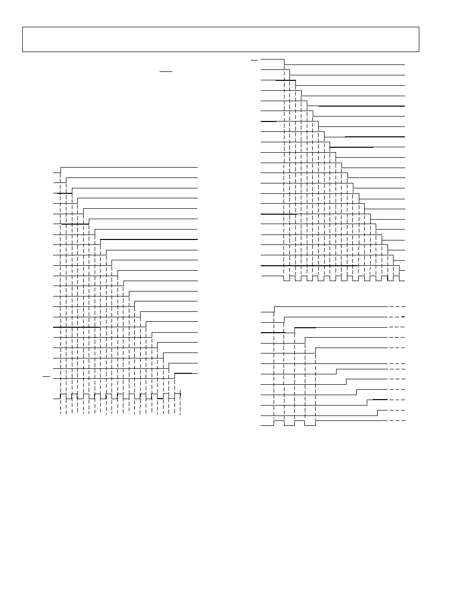
ADM1026
Rev. A | Page 32 of 56
Notes
∑ For a NAND tree test to work, all outputs (INT, RSTMAIN,
RSTSTBY, and PWM) must remain high during the test.
∑ When generating test waveforms, allow for a typical
propagation delay of 500 ns through the NAND tree.
∑ If any of the inputs shown in Figure 56 are unused, they
should not be connected direct to ground, but via a resistor
such as 10 k. This allows the automatic test equipment
(ATE) to drive every input high so that the NAND tree test
can be properly carried out.
GPIO16
GPIO15
GPIO14
GPIO13
GPIO12
GPIO11
GPIO10
GPIO9
GPIO8
FAN0
FAN1
FAN2
FAN3
FAN4
FAN5
FAN6
FAN7
SCL
SDA
CI
INT
NTESTOUT
02657-
A
-
057
Figure 57. NAND Tree Test Taking Inputs High in Turn
In the event of an input being nonfunctional (stuck high or low)
or two inputs shorted together, the output pattern is different.
Some examples are given in Figure 59 through Figure 61.
Figure 59 shows the effect of one input being stuck low. The
output pattern is normal until the stuck input is reached.
Because that input is permanently low, neither it nor any inputs
further up the tree can have any effect on the output.
INT
CI
SDA
SCL
FAN7
FAN6
FAN5
FAN4
FAN3
FAN2
FAN1
FAN0
GPIO8
GPIO9
GPIO10
GPIO11
GPIO12
GPIO13
GPIO14
GPIO15
GPIO16
NTESTOUT
02657-
A
-
058
Figure 58. NAND Tree Test Taking Inputs Low in Turn
GPIO16
GPIO15
GPIO14
GPIO13
GPIO12
GPIO11
GPIO10
GPIO9
GPIO8
FAN0
FAN1
NTESTOUT
02657-
A
-
059
Figure 59. NAND Tree Test with GPIO11 Stuck Low
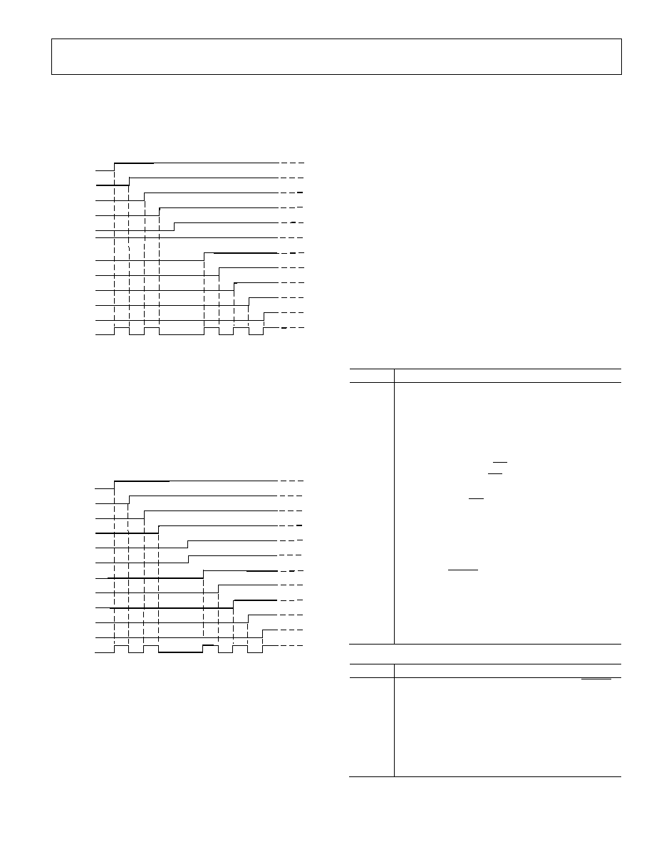
ADM1026
Rev. A | Page 33 of 56
Figure 60 shows the effect of one input being stuck high. Taking
GPIO12 high should take the output high. However, the next
input up the tree, GPIO11, is already high, so the output
immediately goes low again, causing a missing pulse in the
output pattern.
GPIO16
GPIO15
GPIO14
GPIO13
GPIO12
GPIO11
GPIO10
GPIO9
GPIO8
FAN0
FAN1
NTESTOUT
02657-A-060
Figure 60. NAND Tree Test with One Input Stuck High
A similar effect occurs if two adjacent inputs are shorted
together. The example in Figure 61 assumes that the current
sink capability of the circuit driving the inputs is considerably
higher than the source capability, so the inputs are low if either
is low, but high only if both are high.
When GPIO12 goes high the output should go high. But
because GPIO12 and GPIO11 are shorted, they both go high
together, causing a missing pulse in the output pattern.
GPIO16
GPIO15
GPIO14
GPIO13
GPIO12
GPIO11
GPIO10
GPIO9
GPIO8
FAN0
FAN1
NTESTOUT
02657-
A-
061
Figure 61. NAND Tree Test with Two Inputs Shorted
USING THE ADM1026
When power is first applied, the ADM1026 performs a power-
on reset on all its registers (not EEPROM), which sets them to
default conditions as shown in Table 12. In particular, note that
all GPIO pins are configured as inputs to avoid possible
conflicts with circuits trying to drive these pins.
The ADM1026 can also be initialized at any time by writing a
1 to Bit 7 of Configuration Register 1, which sets some registers
to their default power-on conditions. This bit should be cleared
by writing a 0 to it.
After power-on, the ADM1026 must be configured to the user's
specific requirements. This consists of
∑ Writing values to the limit registers.
∑ Configuring Pins 3 to 6, and 9 to 12 as fan inputs or GPIO,
using Configuration Register 2 (Address 01h).
∑ Setting the fan divisors using the fan divisor registers
(Addresses 02h and 03h).
∑ Configuring the GPIO pins for input/output polarity, using
GPIO Configuration Registers 1 to 4 (Addresses 08h to
0Bh) and Bits 6 and 7 of Configuration
Register 3.
∑ Setting mask bits in Mask Registers 1 to 6 (Addresses 18h
to 1Dh) for any inputs that are to be masked out.
∑ Setting up Configuration Registers 1 and 3, as described in
Table 9 and Table 10.
Table 9. Configuration Register 1
Bit Description
0
Controls the monitoring loop of the ADM1026.
Setting Bit 0 low stops the monitoring loop and puts
the ADM1026 into low power mode and reduces
power consumption. Serial bus communication is still
possible with any register in the ADM1026 while in
low power mode. Setting bit 0 high starts the
monitoring loop.
1
Enables or disables the INT interrupt output. Setting
Bit 1 high enables the INT output, setting Bit 1 low
disables the output.
2
Used to clear the INT interrupt output when set high.
GPIO pins and interrupt status register contents are
not affected.
3
Configures Pins 27 and 28 as the second external
temperature channel when 0, and as A
IN8
and A
IN9
when set to 1.
4
Enables the THERM output when set to 1.
5
Enables automatic fan speed control on the DAC
output when set to 1.
6
Enables automatic fan speed control on the PWM
output when set to 1.
7
Performs a soft reset when set to 1.
Table 10. Configuration Register 3
Bit Description
0
Configures Pin 42 as GPIO when set to 1 or as THERM
when cleared to 0.
1
Clears the CI latch when set to 1. Thereafter, a 0 must
be written to allow subsequent CI detection.
2
Selects V
REF
as 2.5 V when set to 1 or as 1.82 V when
cleared to 0.
3≠5 Unused.
6, 7
Set up GPIO16 for direction and polarity.

ADM1026
Rev. A | Page 34 of 56
Starting Conversion
The monitoring function (analog inputs, temperature, and fan
speeds) in the ADM1026 is started by writing to Configuration
Register 1 and setting Start (Bit 0) high. The INT _Enable
(Bit 1) should be set to 1, and INT Clear (Bit 2) set to 0 to
enable interrupts. The THERM enable bit (Bit 4) should be set
to 1 to enable temperature interrupts at the THERM pin. Apart
from initially starting together, the analog measurements and
fan speed measurements proceed independently, and are not
synchronized in any way.
Reduced Power Mode
The ADM1026 can be placed in a low power mode by setting
Bit 0 of the configuration register to 0. This disables the internal
ADC.
Software Reset Function
As previously mentioned, the ADM1026 can be reset in
software by setting Bit 7 of Configuration Register 1 (Reg. 00h)
to 1. Configuration Register 1, 00h, should then be manually
cleared. Note that the software reset differs from a power-on
reset in that only some of the ADM1026 registers are reinitial-
ized to their power-on default values. The registers that are
initialized to their default values by the software reset are
∑ Configuration Registers (Registers 01h to 0Bh)
∑ Mask Registers 1 to 6, internal temperature offset, and
Status Registers 4, 5, and 6 (Registers 18h to 25h)
∑ All value registers (Registers 1Fh, 20h to 3Fh)
∑ External 1 and External 2 Offset Registers (6Eh, 6Fh)
Note that the limit registers (0Dh to 12h, 40h to 6Dh) are not
reset by the software reset function. This can be useful if one
needs to reset the part but does not want to reprogram all
parameters again. Note that a power-on reset initializes all
registers on the ADM1026, including the limit registers.
Application Schematic
Figure 62 shows how the ADM1026 could be used in an
application that requires system management of a PC or server.
Several GPIOs are used to read the VID codes of the CPU. Up
to two CPU temperature measurements can be read back. All
power supply voltages are monitored in the system. Up to eight
fan speeds can be measured, irrespective of whether they are
controlled by the ADM1026 or hardwired to a system supply.
The V
REF
output includes the recommended filtering circuitry.
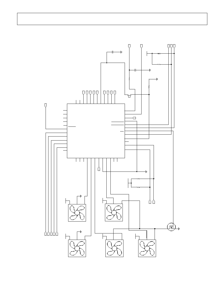
ADM1026
Rev. A | Page 35 of 56
U1
ADM1026_SKT
3.3V STDY
SYS_T
H
ERM
CPU1_VID4
CPU1_VID3
CPU1_VID2
CPU1_VID1
CPU1_VID0
FAN
X1
X3
+
12V
X2
X4
1
2
3
FAN
FAN
X5
Q1
+
12V
1
2
3
+
12V
1
2
3
+
12V
1
2
3
+
12V
1
2
3
FAN
FAN
SDATA
SCL
O
CK
CPURESET
SMB_ALER
T
P
O
WE
R_GOOD
V
CC
0≠2.5V_OUT
V
RE
F
_OUT
R5
10k
3.3V_STBY
CPU1_THERMDC
CPU1_THERMDA
CPU2_THERMDC
CPU2_THERMDA
CPU1_V
CCP
CPU2_V
CCP
+
12 V
IN
≠12 V
IN
+5
V
IN
FAN0/GPIO0
FAN1/GPIO1
FAN2/GPIO2
FAN3/GPIO3
GPIO15
GPIO14
GPIO13
GPIO12
GPIO11
GPIO10
PWM
CI
INT
RESETMAIN
RESETSTBY
DAC
SCL
SDA
ADD
AGND
3.3V STBY
V
REF
24
23
22
21
20
19
18
17
1
2
3
4
5
6
7
8
9
10
11
12
16
15
14
13
FAN4/GPIO4
FAN5/GPIO5
FAN6/GPIO6
FAN7/GPIO7
DGND
GP
IO9
GP
IO8
3.3VMAIN
A
IN4
A
IN3
A
IN2
A
IN1
A
IN0
THERM
37
38
39
40
41
42
43
44
45
46
47
48
A
IN5
A
IN6
A
IN7
+V
CCP
+
12 V
IN
≠12V
IN
+5
V
IN
+V
BA
T
D2+
/
A
IN8
D2≠/A
IN9
D1+
D1≠
36
35
34
33
32
31
30
29
28
27
26
25
S1
4
1
C1 0.1
µ
F
B1
+
R4
10k
R3
470k
R6
10k
R2
2k
R1
2k
02657-
A-
062
Figure 62. ADM1026 Schematic
ADM1026
Rev. A | Page 36 of 56
REGISTERS
Table 11. Address Pointer Register
Bit
Name
R/W
Description
7≠0
Address Pointer
Write
Address of ADM1026 registers. See the following tables for details.
Table 12. List of Registers
Hex
Address
Name
Power-On Value
Description
00
Configuration 1
00h
Configures various operating parameters
01
Configuration 2
00h
Configures Pins 3≠6 and 9≠12 as fan inputs or GPIO
02
Fan 0≠3 Divisor
55h
Sets oscillator frequency for Fan 0≠3 speed measurement
03
Fan 4≠7 Divisor
55h
Sets oscillator frequency for Fan 4≠7 speed measurement
04
DAC Control
FFh
Contains value for fan speed DAC (analog fan speed control) or minimum
value for automatic fan speed control
05
PWM Control
FFh
Contains value for PWM fan speed control or minimum value for automatic
fan speed control
06
EEPROM Register
100h
For factory use only
07
Configuration Register
300h
Configuration register for THERM, V
REF
and GPIO16
08
GPIO Config 1
00h
Configures GPIO0 to GPIO3 as input or output and as active high or active low
09
GPIO Config 2
00h
Configures GPIO4 to GPIO7 as input or output and as active high or active low
0A
GPIO Config 3
00h
Configures GPIO8 to GPIO11 as input or output and as active high or active
low
0B
GPIO Config 4
00h
Configures GPIO12 to GPIO15 as input or output and as active high or active
low
0C
EEPROM Register 2
00h
For factory use only
0D
Int Temp THERM Limit
37h (55∞C)
High limit for THERM interrupt output based on internal temperature
measurement
0E
TDM1 THERM Limit
50h (80∞C)
High limit for THERM interrupt output based on Remote Channel 1 (D1)
temperature measurement
0F
TDM2 THERM Limit
50h (80∞C)
High limit for THERM interrupt output based on Remote Channel 2 (D2)
temperature measurement
10
Int Temp T
MIN
28h (40∞C)
T
MIN
value for automatic fan speed control based on internal temperature
measurement
11
TDM1 T
MIN
40h (64∞C)
T
MIN
value for automatic fan speed control based on Remote Channel 1 (D1)
temperature measurement
12
TDM2 T
MIN
40h (64∞C)
T
MIN
value for automatic fan speed control based on Remote Channel 2 (D2)
temperature measurement
13
EEPROM Register 3
00h
Configures EEPROM for read/write/erase, etc.
14
Test Register 1
00h
Manufacturer's test register
15
Test Register 2
00h
For manufacturer's use only
16
Manufacturer's ID
41h
Contains manufacturer's ID code
17
Revision
4xh
Contains code for major and minor revisions
18
Mask Register 1
00h
Interrupt mask register for temperature and supply voltage faults
19
Mask Register 2
00h
Interrupt mask register for analog input faults
1A
Mask Register 3
00h
Interrupt mask register for fan faults
1B
Mask Register 4
00h
Interrupt mask register for local temp, V
BAT
, A
IN8
, THERM, AFC, CI and GPIO16
1C
Mask Register 5
00h
Interrupt mask register for GPIO0 to GPIO7
1D
Mask Register 6
00h
Interrupt mask register for GPIO8 to GPIO15
1E
Int Temp Offset
00h
Offset register for internal temperature measurement
1F
Int Temp Value
00h
Measured temperature from on≠chip sensor
20
Status Register 1
00h
Interrupt status register for external temp and supply voltage faults
21
Status Register 2
00h
Interrupt status register for analog input faults
22
Status Register 3
00h
Interrupt status register for fan faults
23
Status Register 4
00h
Interrupt status register for local temp, V
BAT
, A
IN8
, THERM, AFC, CI, and GPIO16

ADM1026
Rev. A | Page 37 of 56
Hex
Address
Name
Power-On Value
Description
24
Status Register 5
00h
Interrupt status register for GPIO0 to GPIO7
25
Status Register 6
00h
Interrupt status register for GPIO8 to GPIO15
26
V
BAT
Value
00h
Measured value of V
BAT
27
A
IN8
Value
00h
Measured value of A
IN8
28
TDM1 Value
00h
Measured value of remote temperature channel 1 (D1)
29
TDM2/A
IN9
Value
00h
Measured value of remote temperature channel 2 (D2) or A
IN9
2A
3.3 V STBY Value
00h
Measured value of 3.3 V STBY
2B
3.3 V MAIN Value
00h
Measured value of 3.3 V MAIN
2C
+5 V Value
00h
Measured value of +5 V supply
2D
V
CCP
Value
00h
Measured value of processor core voltage
2E
+12 V Value
00h
Measured value of +12 V supply
2F
-12 V Value
00h
Measured value of
-12 V supply
30
A
IN0
Value
00h
Measured value of A
IN0
31
A
IN1
Value
00h
Measured value of A
IN1
32
A
IN2
Value
00h
Measured value of A
IN2
33
A
IN3
Value
00h
Measured value of A
IN3
34
A
IN4
Value
00h
Measured value of A
IN4
35
A
IN5
Value
00h
Measured value of A
IN5
36
A
IN6
Value
00h
Measured value of A
IN6
37
A
IN7
Value
00h
Measured value of A
IN7
38
FAN0 Value
00h
Measured speed of Fan 0
39
FAN1 Value
00h
Measured speed of Fan 1
3A
FAN2 Value
00h
Measured speed of Fan 2
3B
FAN3 Value
00h
Measured speed of Fan 3
3C
FAN4 Value
00h
Measured speed of Fan 4
3D
FAN5 Value
00h
Measured speed of Fan 5
3E
FAN6 Value
00h
Measured speed of Fan 6
3F
FAN7 Value
00h
Measured speed of Fan 7
40
TDM1 High Limit
64h (100∞C)
High limit for Remote Temperature Channel 1 (D1) measurement
41
TDM2/A
IN9
High Limit
64h (100∞C)
High limit for Remote Temperature Channel 2 (D2) or A
IN9
measurement
42
3.3 V STBY High Limit
FFh
High limit for 3.3 V STBY measurement
43
3.3 V MAIN High Limit
FFh
High limit for 3.3 V MAIN measurement
44
+5 V High Limit
FFh
High limit for +5 V supply measurement
45
V
CCP
High Limit
FFh
High limit for processor core voltage measurement
46
+12 V High Limit
FFh
High limit for +12 V supply measurement
47
-12 V High Limit
FFh
High limit for
-12 V supply measurement
48
TDM1 Low Limit
80h
Low limit for Remote Temperature Channel 1 (D1) measurement
49
TDM2/A
IN9
Low Limit
80h
Low limit for Remote Temperature Channel 2 (D2) or A
IN9
measurement
4A
3.3 V STBY Low Limit
00h
Low limit for 3.3 V STBY measurement
4B
3.3 V MAIN Low Limit
00h
Low limit for 3.3 V MAIN measurement
4C
+5 V Low Limit
00h
Low limit for +5 V supply
4D
V
CCP
Low Limit
00h
Low limit for processor core voltage measurement
4E
+12 V Low Limit
00h
Low limit for +12 V supply measurement
4F
-12 V Low Limit
00h
Low limit for
-12 V supply measurement
50
A
IN0
High Limit
FFh
High limit for A
IN0
measurement
51
A
IN1
High Limit
FFh
High limit for A
IN1
measurement
52
A
IN2
High Limit
FFh
High limit for A
IN2
measurement
53
A
IN3
High Limit
FFh
High limit for A
IN3
measurement
54
A
IN4
High Limit
FFh
High limit for A
IN4
measurement
55
A
IN5
High Limit
FFh
High limit for A
IN5
measurement
56
A
IN6
High Limit
FFh
High limit for A
IN6
measurement
57
A
IN7
High Limit
FFh
High limit for A
IN7
measurement
ADM1026
Rev. A | Page 38 of 56
Hex
Address
Name
Power-On Value
Description
58
A
IN0
Low Limit
00h
Low limit for A
IN0
measurement
59
A
IN1
Low Limit
00h
Low limit for A
IN1
measurement
5A
A
IN2
Low Limit
00h
Low limit for A
IN2
measurement
5B
A
IN3
Low Limit
00h
Low limit for A
IN3
measurement
5C
A
IN4
Low Limit
00h
Low limit for A
IN4
measurement
5D
A
IN5
Low Limit
00h
Low limit for A
IN5
measurement
5E
A
IN6
Low Limit
00h
Low limit for A
IN6
measurement
5F
A
IN7
Low Limit
00h
Low limit for A
IN7
measurement
60
FAN0 High Limit
FFh
High limit for Fan 0 speed measurement (no low limit)
61
FAN1 High Limit
FFh
High limit for Fan 1 speed measurement (no low limit)
62
FAN2 High Limit
FFh
High limit for Fan 2 speed measurement (no low limit)
63
FAN3 High Limit
FFh
High limit for Fan 3 speed measurement (no low limit)
64
FAN4 High Limit
FFh
High limit for Fan 4 speed measurement (no low limit)
65
FAN5 High Limit
FFh
High limit for Fan 5 speed measurement (no low limit)
66
FAN6 High Limit
FFh
High limit for Fan 6 speed measurement (no low limit)
67
FAN7 High Limit
FFh
High limit for Fan 7 speed measurement (no low limit)
68
Int. Temp. High Limit
50h (80∞C)
High limit for local temperature measurement
69
Int. Temp. Low Limit
80h
Low limit for local temperature measurement
6A
V
BAT
High Limit
FFh
High limit for V
BAT
measurement
6B
V
BAT
Low Limit
00h
Low limit for V
BAT
measurement
6C
A
IN8
High Limit
FFh
High limit for A
IN8
measurement
6D
A
IN8
Low Limit
00h
Low limit for A
IN8
measurement
6E
Ext1 Temp Offset
00h
Offset register for Remote Temperature Channel 1
6F
Ext2 Temp Offset
00h
Offset register for Remote Temperature Channel 2
DETAILED REGISTER DESCRIPTIONS
Table 13. Register 00h, Configuration Register 1 (Power-On Default 00h)
Bit Name
R/W
Description
0
Monitor = 0
R/W
When this bit is set the ADM1026 monitors all voltage, temperature and fan channels in a round
robin manner.
1
Int Enable = 0
R/W
When this bit is set, the INT output pin is enabled.
2
Int Clear = 0
R/W
Setting this bit clears an interrupt from the voltage, temperature or fan speed channels. Because
GPIO interrupts are level triggered, this bit has no effect on interrupts originating from GPIO
channels. This bit is cleared by writing a 0 to it. If in monitoring mode voltages, temperatures and
fan speeds continue to be monitored after writing to this bit to clear an interrupt, so an interrupt
may be set again on the next monitoring cycle.
3
Enable Voltage/Ext2 = 0 R/W
When this bit is 1, the ADM1026 monitors voltage (A
IN8
and A
IN9
) on Pins 28 and 27, respectively.
When this bit is 0, the ADM1026 monitors a second thermal diode temperature channel, D2, on
these pins. If the second thermal diode channel is not being used, it is recommended that the bit
be set to 1.
4
Enable THERM = 0
R/W
When this bit is 1, the THERM pin (Pin 42) is asserted (go low) if any of the THERM limits are
exceeded. If THERM is pulled low as an input, the DAC and PWM outputs are forced to full scale
until THERM is taken high.
5
Enable DAC AFC = 0
R/W
When this bit is 1, the DAC output is enabled for automatic fan speed control (AFC) based on
temperature. When this bit is 0, the DAC Output reflects the value in Reg 04h, the DAC Control
Register.
6
Enable PWM AFC = 0
R/W
When this bit is 1, the PWM output is enabled for automatic fan speed control (AFC) based on
temperature. When this bit is 0, the PWM Output reflects the value in Reg 05h, the PWM Control
Register.
7
Software Reset = 0
R/W
Writing a 1 to this bit restores all registers to the power-on defaults. This bit is cleared by writing a
0 to it. For more info, see the Software Reset Function section.
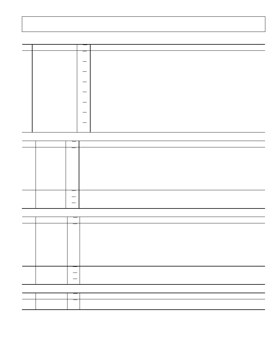
ADM1026
Rev. A | Page 39 of 56
Table 14. Register 01h, Configuration Register 2 (Power-On Default 00h)
Bit Name
R/W
Description
0
Enable GPIO0/Fan0 = 0 R/W
When this bit is 1, Pin 3 is enabled as a general-purpose I/O pin (GPIO0), otherwise it is a fan tach
measurement input (Fan 0).
1
Enable GPIO1/Fan1 = 0 R/W
When this bit is 1, Pin 4 is enabled as a general-purpose I/O pin (GPIO1), otherwise it is a fan tach
measurement input (Fan 1).
2
Enable GPIO2/Fan2 = 0 R/W
When this bit is 1, Pin 5 is enabled as a general-purpose I/O pin (GPIO2), otherwise it is a fan tach
measurement input (Fan 2).
3
Enable GPIO3/Fan3 = 0 R/W
When this bit is 1, Pin 6 is enabled as a general-purpose I/O pin (GPIO3), otherwise it is a fan tach
measurement input (Fan 3).
4
Enable GPIO4/Fan4 = 0 R/W
When this bit is 1, Pin 9 is enabled as a general-purpose I/O pin (GPIO4), otherwise it is a fan tach
measurement input (Fan 4).
5
Enable GPIO5/Fan5 = 0 R/W
When this bit is 1, Pin 10 is enabled as a general-purpose I/O pin (GPIO5), otherwise it is a fan tach
measurement input (Fan 5).
6
Enable GPIO6/Fan6 = 0 R/W
When this bit is 1, Pin 11 is enabled as a general-purpose I/O pin (GPIO6), otherwise it is a fan tach
measurement input (Fan 6).
7
Enable GPIO7/Fan7 = 0 R/W
When this bit is 1, Pin 12 is enabled as a general-purpose I/O pin (GPIO7), otherwise it is a fan tach
measurement input (Fan 7).
Table 15. Register 02h, Fans 0 to 3 Fan Divisor Register (Power-On Default 55h)
Bit
Name
R/W
Description
1≠0
Fan 0 Divisor
R/W
Sets the oscillator prescaler division ratio for Fan 0 speed measurement. The division ratios, oscillator
frequencies, and typical fan speeds (based on 2 tach pulses per revolution) are as follows:
Code
Divide By
Oscillator
Frequency (kHz)
Fan Speed (RPM)
00
1
22.5
8800, nominal, for count of 153
01
2
11.25
4400, nominal, for count of 153
10
4
5.62
2200, nominal, for count of 153
11
8
2.81
1100, nominal, for count of 153
3≠2
Fan 1 Divisor
R/W
Same as Fan 0
5≠4
Fan 2 Divisor
R/W
Same as Fan 0
7≠6
Fan 3 Divisor
R/W
Same as Fan 0
Table 16. Register 03h, Fans 4 to 7 Fan Divisor Register (Power-On Default 55h)
Bit Name
R/W Description
1≠0
Fan 4 Divisor
R/W
Sets the oscillator prescaler division ratio for Fan 4 speed measurement. The division ratios, oscillator
frequencies, and typical fan speeds (based on 2 tach pulses per revolution) are as follows:
Code
Divide By
Oscillator
Frequency (kHz)
Fan Speed (RPM)
00
1
22.5
8800, nominal, for count of 153
01
2
11.25
4400, nominal, for count of 153
10
4
5.62
2200, nominal, for count of 153
11
8
2.81
1100, nominal, for count of 153
3-2
Fan 5 Divisor
R/W
Same as Fan 4
5-4
Fan 6 Divisor
R/W
Same as Fan 4
7-6
Fan 7 Divisor
R/W
Same as Fan 4
Table 17. Register 04h, DAC Control Register (Power-On Default FFh)
Bit
Name
R/W Description
7≠0
DAC Control
R/W
This register contains the value to which the fan speed DAC is programmed in normal mode, or the
4 MSBs contain the minimum fan speed in auto fan speed control mode.
ADM1026
Rev. A | Page 40 of 56
Table 18. Register 05h, PWM Control Register (Power-On Default FFh)
Bit
Name
R/W Description
7≠4
PWM Control
R/W
This register contains the value to which the PWM fan speed is programmed in normal
mode, or the 4 MSBs contain the minimum fan speed in auto fan speed control mode.
0000 = 0% Duty Cycle
0001 = 7% Duty Cycle
0101 = 33% Duty Cycle
0110 = 40% Duty Cycle
0111 = 47% Duty Cycle
1110 = 93% Duty Cycle
1111 = 100% Duty Cycle
3≠0
Unused
R
Undefined
Table 19. Register 06h, EEPROM Register 1 (Power-On Default 00h)
Bit
Name
R/W Description
7≠0
Factory Use
R/W
For factory use only. Do not write to this register.
Table 20. Register 07h, Configuration Register 3 (Power-On Default 00h)
Bit
Name
R/W Description
0
Enable GPIO16/ THERM = 0
R/W
When this bit is 1, Pin 42 is enabled as a general-purpose I/O pin (GPIO16); otherwise it
is the THERM output.
1
CI Clear = 0
R/W
Writing a 1 to this bit clears the CI latch. This bit is cleared by writing a 0 to it.
2
V
REF
Select = 0
R/W
When this bit is 0, V
REF
(Pin 24) outputs 1.82 V, otherwise, it outputs 2.5 V.
5≠3
Unused
R
Undefined, reads back 0.
6
GPIO16 Direction
R/W
When this bit is 0, GPIO16 is configured as an input; otherwise, it is an output.
7
GPIO16 Polarity
R/W
When this bit is 0, GPIO16 is active low; otherwise, it is active high.
Table 21. Register 08h, GPIO Configuration Register 1 (Power-On Default 00h)
Bit
Name
R/W Description
0
GPIO0 Direction
R/W
When this bit is 0, GPIO0 is configured as an input; otherwise, it is an output.
1
GPIO0 Polarity
R/W
When this bit is 0, GPIO0 is active low; otherwise it is active high.
2
GPIO1 Direction
R/W
When this bit is 0, GPIO1 is configured as an input; otherwise, it is an output.
3
GPIO1 Polarity
R/W
When this bit is 0, GPIO1 is active low; otherwise it is active high.
4
GPIO2 Direction
R/W
When this bit is 0, GPIO2 is configured as an input; otherwise, it is an output.
5
GPIO2 Polarity
R/W
When this bit is 0, GPIO2 is active low; otherwise, it is active high.
6
GPIO3 Direction
R/W
When this bit is 0, GPIO3 is configured as an input; otherwise, it is an output.
7
GPIO3 Polarity
R/W
When this bit is 0, GPIO3 is active low; otherwise, it is active high.
Table 22. Register 09h, GPIO Configuration Register 2 (Power-On Default 00h)
Bit
Name
R/W Description
0
GPIO4 Direction
R/W
When this bit is 0, GPIO4 is configured as an input; otherwise, it is an output.
1
GPIO4 Polarity
R/W
When this bit is 0, GPIO4 is active low; otherwise, it is active high.
2
GPIO5 Direction
R/W
When this bit is 0, GPIO5 is configured as an input; otherwise, it is an output.
3
GPIO5 Polarity
R/W
When this bit is 0, GPIO5 is active low; otherwise, it is active high.
4
GPIO6 Direction
R/W
When this bit is 0, GPIO6 is configured as an input; otherwise, it is an output.
5
GPIO6 Polarity
R/W
When this bit is 0, GPIO6 is active low; otherwise, it is active high.
6
GPIO7 Direction
R/W
When this bit is 0, GPIO7 is configured as an input; otherwise, it is an output.
7
GPIO7 Polarity
R/W
When this bit is 0, GPIO7 is active low; otherwise, it is active high.
ADM1026
Rev. A | Page 41 of 56
Table 23. Register 0Ah, GPIO Configuration Register 3 (Power-On Default 00h)
Bit
Name
R/W Description
0
GPIO8 Direction
R/W
When this bit is 0, GPIO8 is configured as an input; otherwise, it is an output.
1
GPIO8 Polarity
R/W
When this bit is 0, GPIO8 is active low; otherwise, it is active high.
2
GPIO9 Direction
R/W
When this bit is 0, GPIO9 is configured as an input; otherwise, it is an output.
3
GPIO9 Polarity
R/W
When this bit is 0, GPIO9 is active low; otherwise, it is active high.
4
GPIO10 Direction
R/W
When this bit is 0, GPIO10 is configured as an input; otherwise, it is an output.
5
GPIO10 Polarity
R/W
When this bit is 0, GPIO10 is active low; otherwise, it is active high.
6
GPIO11 Direction
R/W
When this bit is 0, GPIO11 is configured as an input; otherwise, it is an output.
7
GPIO11 Polarity
R/W
When this bit is 0, GPIO11 is active low; otherwise, it is active high.
Table 24. Register 0Bh, GPIO Configuration Register 4 (Power-On Default 00h)
Bit
Name
R/W Description
0
GPIO12 Direction
R/W
When this bit is 0, GPIO12 is configured as an input; otherwise, it is an output.
1
GPIO12 Polarity
R/W
When this bit is 0, GPIO12 is active low; otherwise, it is active high.
2
GPIO13 Direction
R/W
When this bit is 0, GPIO13 is configured as an input; otherwise, it is an output.
3
GPIO13 Polarity
R/W
When this bit is 0, GPIO13 is active low; otherwise, it is active high.
4
GPIO14 Direction
R/W
When this bit is 0, GPIO14 is configured as an input; otherwise, it is an output.
5
GPIO14 Polarity
R/W
When this bit is 0, GPIO14 is active low; otherwise, it is active high.
6
GPIO15 Direction
R/W
When this bit is 0, GPIO15 is configured as an input; otherwise, it is an output.
7
GPIO15 Polarity
R/W
When this bit is 0, GPIO15 is active low; otherwise, it is active high.
Table 25. Register 0ch, EEPROM Register 2 (Power-On Default 00h)
Bit
Name
R/W Description
7≠0
Factory Use
R
For factory use only. Do not write to this register.
Table 26. Register 0Dh, Internal Temperature THERM Limit (Power-On Default, 37h 55∞C)
Bit
Name
R/W Description
7≠0
Int Temp THERM Limit
R/W
This register contains the THERM limit for the internal temperature channel. Exceeding this limit
causes the THERM output pin to be asserted.
Table 27. Register 0Eh, TDM1 THERM Limit (Power-On Default 50h, 80∞C)
Bit
Name
R/W Description
7≠0
TDM1 THERM Limit
R/W
This register contains the THERM limit for the TDM1 temperature channel. Exceeding this limit
causes the THERM output pin to be asserted.
Table 28. Register 0Fh, TDM2 THERM Limit (Power-On Default 50h, 80∞C)
Bit
Name
R/W Description
7≠0
TDM2 THERM Limit
R/W
This register contains the THERM limit for the TDM2 temperature channel. Exceeding this limit
causes the THERM output pin to be asserted.
Table 29. Register 10h, Internal Temperature T
MIN
(Power-On Default 28h, 40∞C)
Bit
Name
R/W
Description
7≠0
Internal Temp T
MIN
R/W
This register contains the T
MIN
value for automatic fan speed control based on the internal
temperature channel.
Table 30. Register 11h, TDM1 Temperature T
MIN
(Power-On Default 40h, 64∞C)
Bit
Name
R/W Description
7≠0
TDM1 Temp T
MIN
R/W
This register contains the T
MIN
value for automatic fan speed control based on the TDM1
temperature channel.
ADM1026
Rev. A | Page 42 of 56
Table 31. Register 12h, TDM2 Temperature T
MIN
(Power-On Default 40h, 64∞C)
Bit
Name
R/W Description
7≠0
TDM2 Temp T
MIN
R/W
This register contains the T
MIN
value for automatic fan speed control based on the TDM2 temperature
channel.
Table 32. Register 13h, EEPROM Register 3 (Power-On Default 00h)
Bit
Name
R/W
Description
0
Read
R/W
Setting this bit puts the EEPROM into read mode.
1
Write
R/W
Setting this bit puts the EEPROM in write (program) mode.
2
Erase
R/W
Setting this bit puts the EEPROM into erase mode.
3
Write Protect
R/W
Once
Setting this bit protects the EEPROM against accidental writing or erasure. This bit is write-once and
can only be cleared by a power-on reset.
4
Test Mode Bit 0
R/W
Test mode bits. For factory use only
5
Test Mode Bit 1
R/W
Test mode bits. For factory use only.
6
Test Mode Bit 2
R/W
Test mode bits. For factory use only
7
Clock Extend
R/W
Setting this bit enables SMBus clock extension. The ADM1026 can pull SCL low to extend the clock
pulse if it cannot accept any more data. It is recommended to set this bit to 1 to extend the clock
pulse during repeated EEPROM write or block write operations.
Table 33. Register 14h, Manufacturer's Test Register 1 (Power-On Default 00h)
Bit
Name
R/W
Description
7≠0
Manufacturer's Test 1
R/W
This register is used by the manufacturer for test purposes. It should not be read from or written
to in normal operation.
Table 34. Register 15h, Manufacturer's Test Register 2 (Power-On Default 00h)
Bit
Name
R/W
Description
7≠0
Manufacturer's Test 2 R/W
This register is used by the manufacturer for test purposes. It should not be read from or written
to in normal operation.
Table 35. Register 16h, Manufacturer's ID (Power-On Default 41h)
Bit
Name
R/W Description
7≠0
Manufacturer's ID Code
R
This register contains the manufacturer's ID code.
Table 36. Register 17h, Revision Register (Power-On Default 4xh)
Bit
Name
R/W
Description
3≠0
Minor Revision Code
R
This nibble contains the manufacturer's code for minor revisions to the device. Rev 1 = 0h,
Rev 2 = 1h, and so on.
7≠4
Major Revision Code
R
This nibble denotes the generation of the device. For the ADM1026, this nibble reads 4h.
Table 37. Register 18h, Mask Register 1 (Power-On Default 00h)
Bit Name
R/W
Description
0
Ext1 Temp Mask = 0
R/W
When this bit is set, interrupts generated on the Ext1 temperature channel are masked out.
1
Ext2 Temp
R/W
When this bit is set, interrupts generated on the Ext2/A
IN9
channel are masked out.
2
3.3 V STBY Mask = 0
R/W
When this bit is set, interrupts generated on the 3.3 V STBY voltage channel are masked out.
3
3.3 V MAIN Mask = 0
R/W
When this bit is set, interrupts generated on the 3.3 V MAIN voltage channel are masked out.
4
+5 V Mask = 0
R/W
When this bit is set, interrupts generated on the +5 V voltage channel are masked out.
5
V
CCP
Mask = 0
R/W
When this bit is set, interrupts generated on the V
CCP
voltage channel are masked out.
6
+12 V Mask = 0
R/W
When this bit is set, interrupts generated on the +12 V voltage channel are masked out.
7
-12 V Mask = 0
R/W
When this bit is set, interrupts generated on the -12 V voltage channel are masked out.

ADM1026
Rev. A | Page 43 of 56
Table 38. Register 19h, Mask Register 2 (Power-On Default 00h)
Bit
Name
R/W Description
0
A
IN0
Mask = 0
R/W
When this bit is set, interrupts generated on the A
IN0
voltage channel are masked out.
1
A
IN1
Mask = 0
R/W
When this bit is set, interrupts generated on the A
IN1
voltage channel are masked out.
2
A
IN2
Mask = 0
R/W
When this bit is set, interrupts generated on the A
IN2
voltage channel are masked out.
3
A
IN3
Mask = 0
R/W
When this bit is set, interrupts generated on the A
IN3
voltage channel are masked out.
4
A
IN4
Mask = 0
R/W
When this bit is set, interrupts generated on the A
IN4
voltage channel are masked out.
5
A
IN5
Mask = 0
R/W
When this bit is set, interrupts generated on the A
IN5
voltage channel are masked out.
6
A
IN6
Mask = 0
R/W
When this bit is set, interrupts generated on the A
IN6
voltage channel are masked out.
7
A
IN7
Mask = 0
R/W
When this bit is set, interrupts generated on the A
IN7
voltage channel are masked out.
Table 39. Register 1Ah, Mask Register 3 (Power-On Default 00h)
Bit
Name
R/W
Description
0
FAN0 Mask = 0
R/W
When this bit is set, interrupts generated on the FAN0 tach channel are masked out.
1
FAN1 Mask = 0
R/W
When this bit is set, interrupts generated on the FAN1 tach channel are masked out.
2
FAN2 Mask = 0
R/W
When this bit is set, interrupts generated on the FAN2 tach channel are masked out.
3
FAN3 Mask = 0
R/W
When this bit is set, interrupts generated on the FAN3 tach channel are masked out.
4
FAN4 Mask = 0
R/W
When this bit is set, interrupts generated on the FAN4 tach channel are masked out.
5
FAN5 Mask = 0
R/W
When this bit is set, interrupts generated on the FAN5 tach channel are masked out.
6
FAN6 Mask = 0
R/W
When this bit is set, interrupts generated on the FAN6 tach channel are masked out.
7
FAN7 Mask = 0
R/W
When this bit is set, interrupts generated on the FAN7 tach channel are masked out.
Table 40. Register 1Bh, Mask Register 4 (Power-On Default 00h)
Bit Name
R/W Description
0
Int Temp Mask = 0
R/W
When this bit is set, interrupts generated on the internal temperature channel are masked out.
1
V
BAT
Mask = 0
R/W
When this bit is set, interrupts generated on the V
BAT
voltage channel are masked out.
2
A
IN8
Mask = 0
R/W
When this bit is set, interrupts generated on the A
IN8
voltage channel are masked out.
3
THERM Mask = 0
R/W
When this bit is set, interrupts generated from THERM events are masked out.
4
AFC Mask = 0
R/W
When this bit is set, interrupts generated from automatic fan control events are masked out.
5
Unused
R/W
Unused. Reads back 0.
6
CI Mask = 0
R/W
When this bit is set, interrupts generated by the chassis intrusion input are masked out.
7
GPIO16 Mask = 0
R/W
When this bit is set, interrupts generated on the GPIO16 channel are masked out.
Table 41. Register 1Ch, Mask Register 5 (Power-On Default 00h)
Bit
Name
R/W Description
0
GPIO0 Mask = 0
R/W
When this bit is set, interrupts generated on the GPIO0 channel are masked out.
1
GPIO1 Mask = 0
R/W
When this bit is set, interrupts generated on the GPIO1 channel are masked out.
2
GPIO2 Mask = 0
R/W
When this bit is set, interrupts generated on the GPIO2 channel are masked out.
3
GPIO3 Mask = 0
R/W
When this bit is set, interrupts generated on the GPIO3 channel are masked out.
4
GPIO4 Mask = 0
R/W
When this bit is set, interrupts generated on the GPIO4 channel are masked out.
5
GPIO5 Mask = 0
R/W
When this bit is set, interrupts generated on the GPIO5 channel are masked out.
6
GPIO6 Mask = 0
R/W
When this bit is set, interrupts generated on the GPIO6 channel are masked out.
7
GPIO7 Mask = 0
R/W
When this bit is set, interrupts generated on the GPIO7 channel are masked out.
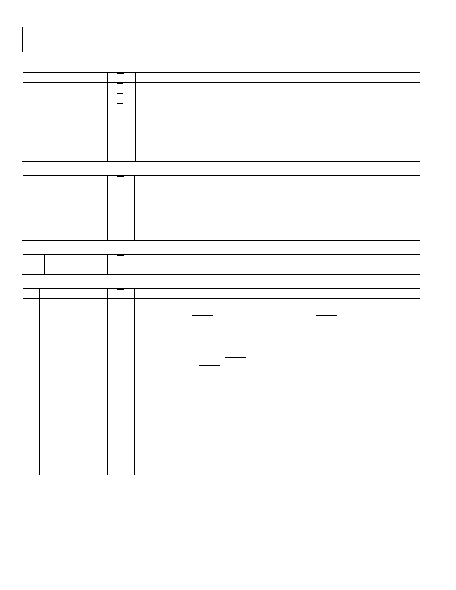
ADM1026
Rev. A | Page 44 of 56
Table 42. Register 1Dh, Mask Register 6 (Power-On Default 00h)
Bit
Name
R/W
Description
0
GPIO8 Mask = 0
R/W
When this bit is set, interrupts generated on the GPIO8 channel are masked out.
1
GPIO9 Mask = 0
R/W
When this bit is set, interrupts generated on the GPIO9 channel are masked out.
2
GPIO10 Mask = 0
R/W
When this bit is set, interrupts generated on the GPIO10 channel are masked out.
3
GPIO11Mask = 0
R/W
When this bit is set, interrupts generated on the GPIO11 channel are masked out.
4
GPIO12 Mask = 0
R/W
When this bit is set, interrupts generated on the GPIO12 channel are masked out.
5
GPIO13 Mask = 0
R/W
When this bit is set, interrupts generated on the GPIO13 channel are masked out.
6
GPIO14 Mask = 0
R/W
When this bit is set, interrupts generated on the GPIO14 channel are masked out.
7
GPIO15 Mask = 0
R/W
When this bit is set, interrupts generated on the GPIO15 channel are masked out.
Table 43. Register 1Eh, INT Temp Offset (Power-On Default 00h)
Bit
Name
R/W Description
7≠0
Int Temp Offset
R/W
This register contains the offset value for the internal temperature channel, a twos complement
result before it is stored or compared to limits. In this way, a sort of one-point calibration can be
done whereby the whole transfer function of the channel can be moved up or down. From a
software point of view, this may be a very simple method to vary the characteristics of the
measurement channel if the thermal characteristics change for any reason (for instance from one
chassis to another), if the measurement point is moved, if a plug-in card is inserted or removed, and
so on.
Table 44. Register 1Fh, INT Temp Measured Value (Power-On Default 00h)
Bit
Name
R/W Description
7≠0
Int Temp Value
R
This register contains the measured value of the internal temperature channel.
Table 45. Register 20h, Status Register 1 (Power-On Default 00h)
Bit Name
R/W
Description
0
Ext1 Temp Status = 0
R
1, if Ext1 value is above the high limit or below the low limit on the previous conversion cycle;
0 otherwise. This bit is set (once only) if a THERM mode is engaged as a result of Ext1 temp readings
exceeding the Ext1 THERM limit. This bit is also set (once only) if THERM mode is disengaged as a
result of Ext1 temperature readings going 5∞C below Ext1 THERM limit.
1
Ext2 Temp Status = 0
R
1, if Ext 2 value (or A
IN9
if in voltage measurement mode) is above the /A
IN9
status = 0 high limit or
below the low limit on the previous conversion cycle; 0 otherwise. This bit is set (once only) if a
THERM mode is engaged as a result of Ext2 temperature readings exceeding the Ext2 THERM limit.
This bit is also set (once only) if THERM mode is disengaged as a result of Ext2 temperature readings
going 5∞C below Ext2 THERM limit.
2
3.3 V STBY Status = 0
R
1, if 3.3 V STBY value is above the high limit or below the low limit on the previous conversion cycle;
0 otherwise.
3
3.3 V MAIN Status = 0 R
1, if 3.3 V MAIN value is above the high limit or below the low limit on the previous conversion
cycle; 0 otherwise.
4
+5 V Status = 0
R
1, if +5 V value is above the high limit or below the low limit on the previous conversion cycle;
0 otherwise.
5
V
CCP
Status = 0
R
1, if V
CCP
value is above the high limit or below the low limit on the previous conversion cycle;
0 otherwise.
6
+12 V Status = 0
R
1, if +12 V value is above the high limit or below the low limit on the previous conversion cycle;
0 otherwise.
7
-12 V Status = 0
R
1, if
-12 V value is above the high limit or below the low limit on the previous conversion cycle;
0 otherwise.

ADM1026
Rev. A | Page 45 of 56
Table 46. Register 21h, Status Register 2 (Power-On Default 00h)
Bit Name
R/W
Description
0
A
IN0
Status = 0
R
1, if A
IN0
to A
IN7
value is above the high limit or below the low limit on the previous conversion
cycle;0 otherwise.
1
A
IN1
Status = 0
R
1, if A
IN0
to A
IN7
value is above the high limit or below the low limit on the previous conversion
cycle;0 otherwise.
2
A
IN2
Status = 0
R
1, if A
IN0
to A
IN7
value is above the high limit or below the low limit on the previous conversion
cycle;0 otherwise.
3
A
IN3
Status = 0
R
1, if A
IN0
to A
IN7
value is above the high limit or below the low limit on the previous conversion
cycle;0 otherwise.
4
A
IN4
Status = 0
R
1, if A
IN0
to A
IN7
value is above the high limit or below the low limit on the previous conversion
cycle;0 otherwise.
5
A
IN5
Status = 0
R
1, if A
IN0
to A
IN7
value is above the high limit or below the low limit on the previous conversion
cycle;0 otherwise.
6
A
IN6
Status = 0
R
1, if A
IN0
to A
IN7
value is above the high limit or below the low limit on the previous conversion
cycle;0 otherwise.
7
A
IN7
Status = 0
R
1, if A
IN0
to A
IN7
value is above the high limit or below the low limit on the previous conversion
cycle;0 otherwise.
Table 47. Register 22h, Status Register 3 (Power-On Default 00h)
Bit
Name
R/W
Description
0
FAN0 Status 1 = 0
R
1, if FAN0 to FAN7 value is above the high limit on the previous conversion cycle; 0 otherwise.
1
FAN1 Status 1 = 0
R
1, if FAN0 to FAN7 value is above the high limit on the previous conversion cycle; 0 otherwise.
2
FAN2 Status 1 = 0
R
1, if FAN0 to FAN7 value is above the high limit on the previous conversion cycle; 0 otherwise.
3
FAN3 Status 1 = 0
R
1, if FAN0 to FAN7 value is above the high limit on the previous conversion cycle; 0 otherwise.
4
FAN4 Status 1 = 0
R
1, if FAN0 to FAN7 value is above the high limit on the previous conversion cycle; 0 otherwise.
5
FAN5 Status 1 = 0
R
1, if FAN0 to FAN7 value is above the high limit on the previous conversion cycle; 0 otherwise.
6
FAN6 Status 1 = 0
R
1, if FAN0 to FAN7 value is above the high limit on the previous conversion cycle; 0 otherwise.
7
FAN7 Status 1 = 0
R
1, if FAN0 to FAN7 value is above the high limit on the previous conversion cycle; 0 otherwise.
Table 48. Register 23h, Status Register 4 (Power-On Default 00h)
Bit Name
R/W Description
0
Int Temp Status = 0
R
1, if Int value is above the high limit or below the low limit on the previous conversion cycle, 0
otherwise. This bit is set (once only) if a THERM mode is engaged as a result of int temperature
readings exceeding the Int THERM limit. This bit is also set (once only) if THERM mode is disengaged
as a result of internal temperature readings going 5∞C below Int THERM limit.
1
V
BAT
Status = 0
R
1, if V
BAT
value is above the high limit or below the low limit on the previous conversion cycle,
0 otherwise.
2
A
IN8
Status = 0
R
1, if A
IN8
value is above the high limit or below the low limit on the previous conversion cycle,
0 otherwise.
3
THERM Status = 0
R
This bit is set (once only) if a THERM mode is engaged as a result of temperature readings
exceeding the THERM limits on any channel. This bit is also set (once only) if THERM mode is
disengaged as a result of temperature readings going 5∞C below THERM limits on any channel.
4
AFC Status = 0
R
This bit is set (once only) if the fan turns on when in automatic fan speed control (AFC) mode as a
result of a temperature reading exceeding T
MIN
on any channel. This bit is also set (once only) if the
fan turns off when in automatic fan speed control mode.
5
Unused
R
Unused. Reads back 0.
6
CI Status = 0
R
This bit latches a chassis intrusion event.
7
GPIO16 Status = 0
R
When GPIO16 is configured as an input, this bit is set when GPIO16 is asserted. (Asserted may be
active high or active low depending on the setting in GPIO configuration register.)
R/W
When GPIO16 is configured as an output, setting this bit asserts GPIO16. (Asserted may be active
high or active low depending on setting in GPIO configuration register.)

ADM1026
Rev. A | Page 46 of 56
Table 49. Register 24h, Status Register 5 (Power-On Default 00h)
Bit Name
R/W
1
Description
0
GPIO0 Status = 0
R
When GPIO0 is configured as an input, this bit is set when GPIO0 is asserted. (Asserted may be
active high or active low depending on setting of Bit 1 in GPIO Configuration Register 1.)
R/W
When GPIO0 is configured as an output, setting this bit asserts GPIO0. (Asserted may be active high
or active low depending on setting of Bit 1 in GPIO Configuration Register 1.)
1
GPIO1 Status = 0
R
When GPIO1 is configured as an input, this bit is set when GPIO1 is asserted. (Asserted may be
active high or active low depending on setting of Bit 3 in GPIO Configuration Register 1.)
R/W
When GPIO1 is configured as an output, setting this bit asserts GPIO1. (Asserted may be active high
or active low depending on setting of Bit 3 in GPIO Configuration Register 1.)
2
GPIO2 Status = 0
R
When GPIO2 is configured as an input, this bit is set when GPIO2 is asserted. (Asserted may be
active high or active low depending on setting of Bit 5 in GPIO Configuration Register 1.)
R/W
When GPIO2 is configured as an output, setting this bit asserts GPIO2. (Asserted may be active high
or active low depending on setting of Bit 5 in GPIO Configuration Register 1.)
3
GPIO3 Status = 0
R
When GPIO3 is configured as an input, this bit is set when GPIO3 is asserted. (Asserted may be
active high or active low depending on setting of Bit 7 in GPIO Configuration Register 1.)
R/W
When GPIO3 is configured as an output, setting this bit asserts GPIO3. (Asserted may be active high
or active low depending on setting of Bit 7 in GPIO Configuration Register 1.)
4
GPIO4 Status = 0
R
When GPIO4 is configured as an input, this bit is set when GPIO4 is asserted. (Asserted may be
active high or active low depending on setting of Bit 1 in GPIO Configuration Register 2.)
R/W
When GPIO4 is configured as an output, setting this bit asserts GPIO4. (Asserted may be active high
or active low depending on setting of Bit 1 in GPIO Configuration Register 2.)
5
GPIO5 Status = 0
R
When GPIO5 is configured as an input, this bit is set when GPIO5 is asserted. (Asserted may be
active high or active low depending on setting of Bit 3 in GPIO Configuration Register 2.)
R/W
When GPIO5 is configured as an output, setting this bit asserts GPIO5. (Asserted may be active high
or active low depending on setting of Bit 3 in GPIO Configuration Register 2.)
6
GPIO6 Status = 0
R
When GPIO6 is configured as an input, this bit is set when GPIO6 is asserted. (Asserted may be
active high or active low depending on setting of Bit 5 in GPIO Configuration Register 2.)
R/W
When GPIO6 is configured as an output, setting this bit asserts GPIO6. (Asserted may be active high
or active low depending on setting of Bit 5 in GPIO Configuration Register 2.)
7
GPIO7 Status = 0
R
When GPIO7 is configured as an input, this bit is set when GPIO7 is asserted. (Asserted may be
active high or active low depending on setting of Bit 7 in GPIO Configuration Register 2.)
R/W
When GPIO7 is configured as an output, setting this bit asserts GPIO7. (Asserted may be active high
or active low depending on setting of Bit 7 in GPIO Configuration Register 2.)
1
GPIO status bits can be written only when a GPIO pin is configured as output. Read-only otherwise.
ADM1026
Rev. A | Page 47 of 56
Table 50. Register 25h, Status Register 6 (Power-On Default 00h)
Bit Name
R/W
1
Description
0
GPIO8 Status = 0
R
When GPIO8 is configured as an input, this bit is set when GPIO8 is asserted. (Asserted may be active
high or active low depending on setting of Bit 1 in GPIO Configuration Register 3.)
R/W
When GPIO8 is configured as an output, setting this bit asserts GPIO8. (Asserted may be active high or
active low depending on setting of Bit 1 in GPIO Configuration Register 3.)
1
GPIO9 Status = 0
R
When GPIO9 is configured as an input, this bit is set when GPIO9 is asserted. (Asserted may be active
high or active low depending on setting of Bit 3 in GPIO Configuration Register 3.)
R/W
When GPIO9 is configured as an output, setting this bit asserts GPIO9. (Asserted may be active high or
active low depending on setting of Bit 3 in GPIO Configuration Register 3.)
2
GPIO10 Status = 0
R
When GPIO10 is configured as an input, this bit is set when GPIO10 is asserted. (Asserted may be
active high or active low depending on setting of Bit 5 in GPIO Configuration Register 3.)
R/W
When GPIO10 is configured as an output, setting this bit asserts GPIO10. (Asserted may be active high
or active low depending on setting of Bit 5 in GPIO Configuration Register 3.)
3
GPIO11 Status = 0
R
When GPIO11 is configured as an input, this bit is set when GPIO11 is asserted. (Asserted may be
active high or active low depending on setting of Bit 7 in GPIO Configuration Register 3.)
R/W
When GPIO11 is configured as an output, setting this bit asserts GPIO11. (Asserted may be active high
or active low depending on setting of Bit 7 in GPIO Configuration Register 3.)
4
GPIO12 Status = 0
R
When GPIO12 is configured as an input, this bit is set when GPIO12 is asserted. (Asserted may be
active high or active low depending on setting of Bit 1 in GPIO Configuration Register 4.)
R/W
When GPIO12 is configured as an output, setting this bit asserts GPIO12. (Asserted may be active high
or active low depending on setting of Bit 1 in GPIO Configuration Register 4.)
5
GPIO13 Status = 0
R
When GPIO13 is configured as an input , this bit is set when GPIO13 is asserted. (Asserted may be
active high or active low depending on setting of Bit 3 in GPIO Configuration Register 4.)
R/W
When GPIO13 is configured as an output, setting this bit asserts GPIO13. (Asserted may be active high
or active low depending on setting of Bit 3 in GPIO Configuration Register 4.)
6
GPIO14 Status = 0
R
When GPIO14 is configured as an input , this bit is set when GPIO14 is asserted. (Asserted may be
active high or active low depending on setting of Bit 5 in GPIO Configuration Register 4.)
R/W
When GPIO14 is configured as an output, setting this bit asserts GPIO14. (Asserted may be active high
or active low depending on setting of Bit 5 in GPIO Configuration Register 4.)
7
GPIO15 Status = 0
R
When GPIO15 is configured as an input, this bit is set when GPIO15 is asserted. (Asserted may be
active high or active low depending on setting of Bit 7 in GPIO Configuration Register 4.)
R/W
When GPIO15 is configured as an output, setting this bit asserts GPIO15. (Asserted may be active high
or active low depending on setting of Bit 7 in GPIO Configuration Register 4.)
1
GPIO status bits can be written only when a GPIO pin is configured as output. Read-only otherwise.
Table 51. Register 26h, V
BAT
Measured Value (Power-On Default 00h)
Bit Name
R/W Description
7≠0 V
BAT
Value
R
This register contains the measured value of the V
BAT
analog input channel.
Table 52. Register 27h, A
IN8
Measured Value (Power-On Default 00h)
Bit
Name
R/W Description
7≠0
A
IN8
Value
R
This register contains the measured value of the A
IN8
analog input channel.
Table 53. Register 28h, EXT1 Measured Value (Power-On Default 00h)
Bit Name
R/W Description
7≠0
Ext1 Value
R
This register contains the measured value of the Ext1 Temp channel.
Table 54. Register 29h, EXT2/A
IN9
Measured Value (Power-On Default 00h)
Bit
Name
R/W Description
7≠0
Ext2 Temp/ A
IN9
Low Limit
R
This register contains the measured value of the Ext2 Temp/A
IN9
channel depending on
which bit is configured.

ADM1026
Rev. A | Page 48 of 56
Table 55. Register 2Ah, 3.3 V STBY Measured Value (Power-On Default 00h)
Bit Name
R/W Description
7≠0
3.3 V STBY Value
R
This register contains the measured value of the 3.3 V STBY voltage.
Table 56. Register 2Bh, 3.3 V MAIN Measured Value (Power-On Default 00h)
Bit Name
R/W Description
7≠0
3.3 V MAIN Value
R
This register contains the measured value of the 3.3 V MAIN voltage.
Table 57. Register 2Ch, +5 V Measured Value (Power-On Default 00h)
Bit Name
R/W Description
7≠0
+5 V Value
R
This register contains the measured value of the +5 V analog input channel.
Table 58. Register 2Dh, VCCP Measured Value (Power-On Default 00h)
Bit Name
R/W Description
7≠0 V
CCP
Value
R
This register contains the measured value of the V
CCP
analog input channel.
Table 59. Register 2Eh, +12V Measured Value (Power-On Default 00h)
Bit Name
R/W Description
7≠0
+12 V Value
R
This register contains the measured value of the +12 V analog input channel.
Table 60. Register 2Fh, ≠12V Measured Value (Power-On Default 00h)
Bit Name
R/W Description
7≠0
≠12 V Value
R
This register contains the measured value of the
-12 V analog input channel.
Table 61. Register 30h, A
IN0
Measured Value (Power-On Default 00h)
Bit Name
R/W Description
7≠0 A
IN0
Value
R
This register contains the measured value of the A
IN0
analog input channel.
Table 62. Register 31h, A
IN1
Measured Value (Power-On Default 00h)
Bit Name
R/W Description
7≠0 A
IN1
Value
R
This register contains the measured value of the A
IN1
analog input channel.
Table 63. Register 32h, A
IN2
Measured Value (Power-On Default 00h)
Bit Name
R/W Description
7≠0 A
IN2
Value
R
This register contains the measured value of the A
IN2
analog input channel.
Table 64. Register 33h, A
IN3
Measured Value (Power-On Default 00h)
Bit Name
R/W Description
7≠0 A
IN3
Value
R
This register contains the measured value of the A
IN3
analog input channel.
Table 65. Register 34h, A
IN4
Measured Value (Power-On Default 00h)
Bit Name
R/W Description
7≠0 A
IN4
Value
R
This register contains the measured value of the A
IN4
analog input channel.
Table 66. Register 35h, A
IN5
Measured Value (Power-On Default 00h)
Bit Name
R/W Description
7≠0 A
IN5
Value
R
This register contains the measured value of the A
IN5
analog input channel.
Table 67. Register 36h, A
IN6
Measured Value (Power-On Default 00h)
Bit Name
R/W Description
7≠0 A
IN6
Value
R
This register contains the measured value of the A
IN6
analog input channel.
Table 68. Register 37h, A
IN7
Measured Value (Power-On Default 00h)
Bit Name
R/W Description
7≠0 A
IN7
Value
R
This register contains the measured value of the A
IN7
analog input channel.
ADM1026
Rev. A | Page 49 of 56
Table 69. Register 38h, FAN0 Measured Value (Power-On Default 00h)
Bit Name
R/W Description
7≠0
FAN0 Value
R
This register contains the measured value of the FAN0 tach input channel.
Table 70. Register 39h, FAN1 Measured Value (Power-On Default 00h)
Bit Name
R/W Description
7≠0
FAN1 Value
R
This register contains the measured value of the FAN1 tach input channel.
Table 71. Register 3Ah, FAN2 Measured Value (Power-On Default 00h)
Bit Name
R/W Description
7≠0
FAN2 Value
R
This register contains the measured value of the FAN2 tach input channel.
Table 72. Register 3Bh, FAN3 Measured Value (Power-On Default 00h)
Bit Name
R/W Description
7≠0
FAN3 Value
R
This register contains the measured value of the FAN3 tach input channel.
Table 73. Register 3Ch, FAN4 Measured Value (Power-On Default 00h)
Bit Name
R/W Description
7≠0
FAN4 Value
R
This register contains the measured value of the FAN4 tach input channel.
Table 74. Register 3Dh, FAN5 Measured Value (Power-On Default 00h)
Bit Name
R/W Description
7≠0
FAN5 Value
R
This register contains the measured value of the FAN5 tach input channel.
Table 75. Register 3Eh, FAN6 Measured Value (Power-On Default 00h)
Bit Name
R/W Description
7≠0
FAN6 Value
R
This register contains the measured value of the FAN6 tach input channel.
Table 76. Register 3Fh, FAN7 Measured Value (Power-On Default 00h)
Bit Name
R/W Description
7≠0
FAN7 Value
R
This register contains the measured value of the FAN7 tach input channel.
Table 77. Register 40h, Ext1 High Limit (Power-On Default 64h/100∞C)
Bit Name
R/W Description
7≠0
Ext1 High Limit
R/W
This register contains the high limit of the Ext1 Temp channel.
Table 78. Register 41h, Ext2/A
IN9
High Limit (Power-On Default 64h/100∞C)
Bit Name
R/W Description
7≠0
Ext2 Temp/ A
IN9
High
Limit
R/W
This register contains the high limit of the Ext2 Temp/A
IN9
channel depending on which one
is configured.
Table 79. Register 42h, 3.3 V STBY High Limit (Power-On Default FFh)
Bit Name
R/W Description
7≠0
3.3 V STBY High Limit
R/W
This register contains the high limit of the 3.3 V STBY analog input channel.
Table 80. Register 43h, 3.3 V MAIN High Limit (Power-On Default FFh)
Bit Name
R/W Description
7≠0
3.3 V MAIN High Limit
R/W
This register contains the high limit of the 3.3 V MAIN analog input channel.
Table 81. Register 44h, +5 V High Limit (Power-On Default FFh)
Bit Name
R/W Description
7≠0
+5 V High Limit
R/W
This register contains the high limit of the +5 V analog input channel.
Table 82. Register 45h, V
CCP
High Limit (Power-On Default FFh)
Bit Name
R/W Description
7≠0 V
CCP
High Limit
R/W
This register contains the high limit of the V
CCP
analog input channel.

ADM1026
Rev. A | Page 50 of 56
Table 83. Register 46h, +12 V High Limit (Power-On Default FFh)
Bit Name
R/W Description
7≠0
+12 V High Limit
R/W
This register contains the high limit of the +12 V analog input channel.
Table 84. Register 47h, -12 V High Limit (Power-On Default FFh)
Bit Name
R/W Description
7≠0
-12V High Limit
R/W
This register contains the high limit of the
-12 V analog input channel.
Table 85. Register 48h, Ext1 Low Limit (Power-On Default 80h)
Bit Name
R/W Description
7≠0
Ext1 Low Limit
R/W
This register contains the low limit of the Ext1 Temp channel.
Table 86. Register 49h, Ext2 / A
IN9
Low Limit (Power-On-Default 80h)
Bit Name
R/W Description
7≠0
Ext2 Temp /A
IN9
Low
Limit
R/W
This register contains the low limit of the Ext2 Temp/A
IN9
channel depending on which bit is
configured.
Table 87. Register 4Ah, 3.3 V STBY Low Limit (Power-On Default 00h)
Bit Name
R/W Description
7≠0
3.3 V STBY Low Limit
R/W
This register contains the low limit of the 3.3 V STBY analog input channel.
Table 88. Register 4Bh, 3.3 V MAIN Low Limit (Power-On Default 00h)
Bit Name
R/W Description
7≠0
3.3 V MAIN Low Limit
R/W
This register contains the low limit of the 3.3 V MAIN analog input channel.
Table 89. Register 4Ch, +5V Low Limit (Power-On Default 00h)
Bit Name
R/W Description
7≠0
0+5 V Low Limit
R/W
This register contains the low limit of the +5 V analog input channel.
Table 90. Register 4Dh, V
CCP
Low Limit (Power-On Default 00h)
Bit Name
R/W Description
7≠0 V
CCP
Low Limit
R/W
This register contains the low limit of the V
CCP
analog input channel.
Table 91. Register 4Eh, +12V Low Limit (Power-On Default 00h)
Bit Name
R/W Description
7≠0
+12 V Low Limit
R/W
This register contains the low limit of the +12 V analog input channel.
Table 92. Register 4Fh, ≠12V Low Limit (Power-On Default 00h)
Bit Name
R/W Description
7≠0
-12 V Low Limit
R/W
This register contains the low limit of the
-12 V analog input channel.
Table 93. Register 50h, A
IN0
High Limit (Power-On Default FFh)
Bit Name
R/W Description
7≠0 A
IN0
High Limit
R/W
This register contains the high limit of the A
IN0
analog input channel.
Table 94. Register 51h, A
IN1
High Limit (Power-On Default FFh)
Bit Name
R/W Description
7≠0 A
IN1
High Limit
R/W
This register contains the high limit of the A
IN1
analog input channel.
Table 95. Register 52h, A
IN2
High Limit (Power-On Default FFh)
Bit Name
R/W Description
7≠0 A
IN2
High Limit
R/W
This register contains the high limit of the A
IN2
analog input channel.
Table 96. Register 53h, A
IN3
High Limit (Power-On Default FFh)
Bit Name
R/W Description
7≠0 A
IN3
High Limit
R/W
This register contains the high limit of the A
IN3
analog input channel.

ADM1026
Rev. A | Page 51 of 56
Table 97. Register 54h, A
IN4
High Limit (Power-On Default FFh)
Bit Name
R/W Description
7≠0 A
IN4
High Limit
R/W
This register contains the high limit of the A
IN4
analog input channel.
Table 98. Register 55h, A
IN5
High Limit (Power-On Default FFh)
Bit Name
R/W Description
7≠0 A
IN5
High Limit
R/W
This register contains the high limit of the A
IN5
analog input channel.
Table 99. Register 56h, A
IN6
High Limit (Power-On Default FFh)
Bit Name
R/W Description
7≠0 A
IN6
High Limit
R/W
This register contains the high limit of the A
IN6
analog input channel.
Table 100. Register 57h, A
IN7
High Limit (Power-On Default FFh)
Bit Name
R/W Description
7≠0 A
IN7
High Limit
R/W
This register contains the high limit of the A
IN7
analog input channel.
Table 101. Register 58h, A
IN0
Low Limit (Power-On Default 00h)
Bit Name
R/W Description
7≠0 A
IN0
Low Limit
R/W
This register contains the low limit of the A
IN0
analog input channel.
Table 102. Register 59h, A
IN1
Low Limit (Power-On Default 00h)
Bit Name
R/W Description
7≠0 A
IN1
Low Limit
R/W
This register contains the low limit of the A
IN1
analog input channel.
Table 103. Register 5Ah, A
IN2
Low Limit (Power-On Default 00h)
Bit Name
R/W Description
7≠0 A
IN2
Low Limit
R/W
This register contains the low limit of the A
IN2
analog input channel.
Table 104. Register 5Bh, A
IN3
Low Limit (Power-On Default 00h)
Bit Name
R/W Description
7≠0 A
IN3
Low Limit
R/W
This register contains the low limit of the A
IN3
analog input channel.
Table 105. Register 5Ch, A
IN4
Low Limit (Power-On Default 00h)
Bit Name
R/W Description
7≠0 A
IN4
Low Limit
R/W
This register contains the low limit of the A
IN4
analog input channel.
Table 106. Register 5Dh, A
IN5
Low Limit (Power-On Default 00h)
Bit Name
R/W Description
7≠0 A
IN5
Low Limit
R/W
This register contains the low limit of the A
IN5
analog input channel.
Table 107. Register 5Eh, A
IN6
Low Limit (Power-On Default 00h)
Bit Name
R/W Description
7≠0 A
IN6
Low Limit
R/W
This register contains the low limit of the A
IN6
analog input channel.
Table 108. Register 5Fh, A
IN7
Low Limit (Power-On Default 00h)
Bit Name
R/W Description
7≠0 A
IN7
Low Limit
R/W
This register contains the low limit of the A
IN7
analog input channel.
Table 109. Register 60h, FAN0 High Limit (Power-On Default FFh)
Bit Name
R/W Description
7≠0
FAN0 High Limit
R/W
This register contains the high limit of the FAN0 tach channel.
Table 110. Register 61h, FAN1 High Limit (Power-On Default FFh)
Bit Name
R/W Description
7≠0
FAN1 High Limit
R/W
This register contains the high limit of the FAN1 tach channel.

ADM1026
Rev. A | Page 52 of 56
Table 111. Register 62h, FAN2 High Limit (Power-On Default FFh)
Bit Name
R/W Description
7≠0
FAN2 High Limit
R/W
This register contains the high limit of the FAN2 tach channel.
Table 112. Register 63h, FAN3 High Limit (Power-On Default FFh)
Bit Name
R/W Description
7≠0
FAN3 High Limit
R/W
This register contains the high limit of the FAN3 tach channel.
Table 113. Register 64h, FAN4 High Limit (Power-On Default FFh)
Bit Name
R/W Description
7≠0
FAN4 High Limit
R/W
This register contains the high limit of the FAN4 tach channel.
Table 114. Register 65h, FAN5 High Limit (Power-On Default FFh)
Bit Name
R/W Description
7≠0
FAN5 High Limit
R/W
This register contains the high limit of the FAN5 tach channel.
Table 115. Register 66h, FAN6 High Limit (Power-On Default FFh)
Bit Name
R/W Description
7≠0
FAN6 High Limit
R/W
This register contains the high limit of the FAN6 tach channel.
Table 116. Register 67h, FAN7 High Limit (Power-On Default FFh)
Bit Name
R/W Description
7≠0
FAN7 High Limit
R/W
This register contains the high limit of the FAN7 tach channel.
Table 117. Register 68h, Int Temp High Limit (Power-On Default 50h (80∞C))
Bit Name
R/W Description
7≠0
Int Temp High Limit
R/W
This register contains the high limit of the internal temperature channel.
Table 118. Register 69h, Int Temp Low Limit (Power-On Default 80h)
Bit Name
R/W Description
7≠0
Int Temp Low Limit
R/W
This register contains the low limit of the internal temperature channel.
Table 119. Register 6Ah, V
BAT
High Limit (Power-On Default FFh)
Bit Name
R/W Description
7≠0 V
BAT
High Limit
R/W
This register contains the high limit of the V
BAT
analog input channel.
Table 120. Register 6Bh, V
BAT
Low Limit (Power-On Default 00h)
Bit Name
R/W Description
7≠0 V
BAT
Low Limit
R/W
This register contains the low limit of the V
BAT
analog input channel.
Table 121. Register 6Ch, A
IN8
High Limit (Power-On Default FFh)
Bit Name
R/W Description
7≠0 A
IN8
High Limit
R/W
This register contains the high limit of the A
IN8
analog input channel.
Table 122. Register 6Dh,
AIN8
Low Limit (Power-On Default 00h)
Bit Name
R/W Description
7≠0 A
IN8
Low Limit
R/W
This register contains the low limit of the A
IN8
analog input channel.

ADM1026
Rev. A | Page 53 of 56
Table 123. Register 6Eh, Ext1 Temp Offset (Power-On Default 00h)
Bit
Name
R/W
Description
7≠0
Ext1 Temp Offset
R/W
This register contains the offset value for the external 1 temperature channel. A twos complement
number can be written to this register, which is then added to the measured result before it is
stored or compared to limits. In this way, a sort of one-point calibration can be done whereby the
whole transfer function of the channel can be moved up or down. From a software point of view,
this may be a very simple method to vary the characteristics of the measurement channel if the
thermal characteristics change for any reason (for instance from one chassis to another), if the
measurement point is moved, if a plug-in card is inserted or removed, and so on.
Table 124. Register 6Fh, Ext2 Temp Offset (Power-On Default 00h)
Bit
Name
R/W Description
7≠0
Ext2 Temp Offset
R/W
This register contains the offset value for the external 2 temperature channel. A twos complement
number can be written to this register, which is then added to the measured result before it is
stored or compared to limits. In this way, a sort of one-point calibration can be done whereby the
whole transfer function of the channel can be moved up or down. From a software point of view,
this may be a very simple method to vary the characteristics of the measurement channel if the
thermal characteristics change for any reason (for instance from one chassis to another), if the
measurement point is moved, if a plug-in card is inserted or removed, and so on.
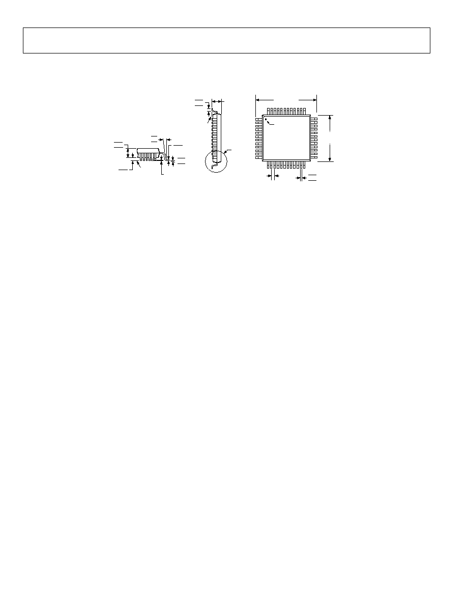
ADM1026
Rev. A | Page 54 of 56
OUTLINE DIMENSIONS
TOP VIEW
(PINS DOWN)
1
12
13
25
24
36
37
48
0.27
0.22
0.17
0.50
BSC
7.00
BSC SQ
SEATING
PLANE
1.60
MAX
0.75
0.60
0.45
VIEW A
9.00 BSC
SQ
PIN 1
0.20
0.09
1.45
1.40
1.35
0.08 MAX
COPLANARITY
VIEW A
ROTATED 90
∞
CCW
SEATING
PLANE
10∞
6∞
2∞
7∞
3.5∞
0∞
0.15
0.05
COMPLIANT TO JEDEC STANDARDS MS-026BBC
Figure 63. 48-Lead Thin Plastic Quad Flat Package [LQFP]
7 mm x 7 mm x 1.4 mm Thick (ST-48)
Dimensions shown in millimeters

ADM1026
Rev. A | Page 55 of 56
ORDERING GUIDE
Model
Temperature Range
Package Description
Package Option
ADM1026JST
0∞C to 100∞C
48-Lead LQFP
ST-48
ADM1026JST-REEL
0∞C to 100∞C
48-Lead LQFP
ST-48
ADM1026JST-REEL7
0∞C to 100∞C
48-Lead LQFP
ST-48
ADM1026JSTZ-REEL
1
0∞C to 100∞C
48-Lead LQFP
ST-48
EVAL-ADM1026EB
Evaluation
Board
1
Z = Pb-free part.

ADM1026
Rev. A | Page 56 of 56
NOTES
© 2004 Analog Devices, Inc. All rights reserved. Trademarks and
registered trademarks are the property of their respective owners.
C02657-0-3/04(A)