Super SequencerTM with Margining Control
and Auxiliary ADC Inputs
ADM1066
Rev. 0
Information furnished by Analog Devices is believed to be accurate and reliable.
However, no responsibility is assumed by Analog Devices for its use, nor for any
infringements of patents or other rights of third parties that may result from its use.
Specifications subject to change without notice. No license is granted by implication
or otherwise under any patent or patent rights of Analog Devices. Trademarks and
registered trademarks are the property of their respective owners.
One Technology Way, P.O. Box 9106, Norwood, MA 02062-9106, U.S.A.
Tel: 781.329.4700
www.analog.com
Fax: 781.326.8703
© 2004 Analog Devices, Inc. All rights reserved.
FEATURES
Complete supervisory and sequencing solution for up to
10 supplies
10 supply fault detectors enable supervision of supplies to
better than 1% accuracy
5 selectable input attenuators allow supervision:
Supplies up to 14.4 V on VH
Supplies up to 6 V on VP1≠4
5 dual-function inputs, VX1≠5:
High impedance input to supply fault detector with
thresholds between 0.573 V and 1.375 V
General-purpose logic input
10 programmable output drivers (PDO1≠10):
Open collector with external pull-up
Push/pull output, driven to VDDCAP or VPn
Open collector with weak pull-up to VDDCAP or VPn
Internally charge-pumped high drive for use with external
N-FET (PDO1≠6 only)
Sequencing engine (SE) implements state machine control of
PDO outputs:
State changes conditional on input events
Enables complex control of boards
Power-up and power-down sequence control
Fault event handling
Interrupt generation on warnings
Watchdog function can be integrated in SE
Program software control of sequencing through SMBus
Complete voltage margining solution for 6 voltage rails
6 voltage output 8-bit DACs (0.300 V to 1.551 V) allow
voltage adjustment via dc/dc converter trim/feedback
node
12-bit ADC for readback of all supervised voltages
2 auxiliary (single-ended) ADC inputs
Reference input, REFIN, has 2 input options:
Driven directly from 2.048V (±0.25%) REFOUT pin
More accurate external reference for improved ADC
performance
Device powered by the highest of VP1≠4, VH for improved
redundancy
User EEPROM: 256 bytes
Industry-standard 2-wire bus interface (SMBus)
Guaranteed PDO low with VH, VPn = 1.2 V
40-lead 6 mm ◊ 6 mm LFCSP and
48-lead 7 mm ◊ 7 mm TQFP packages
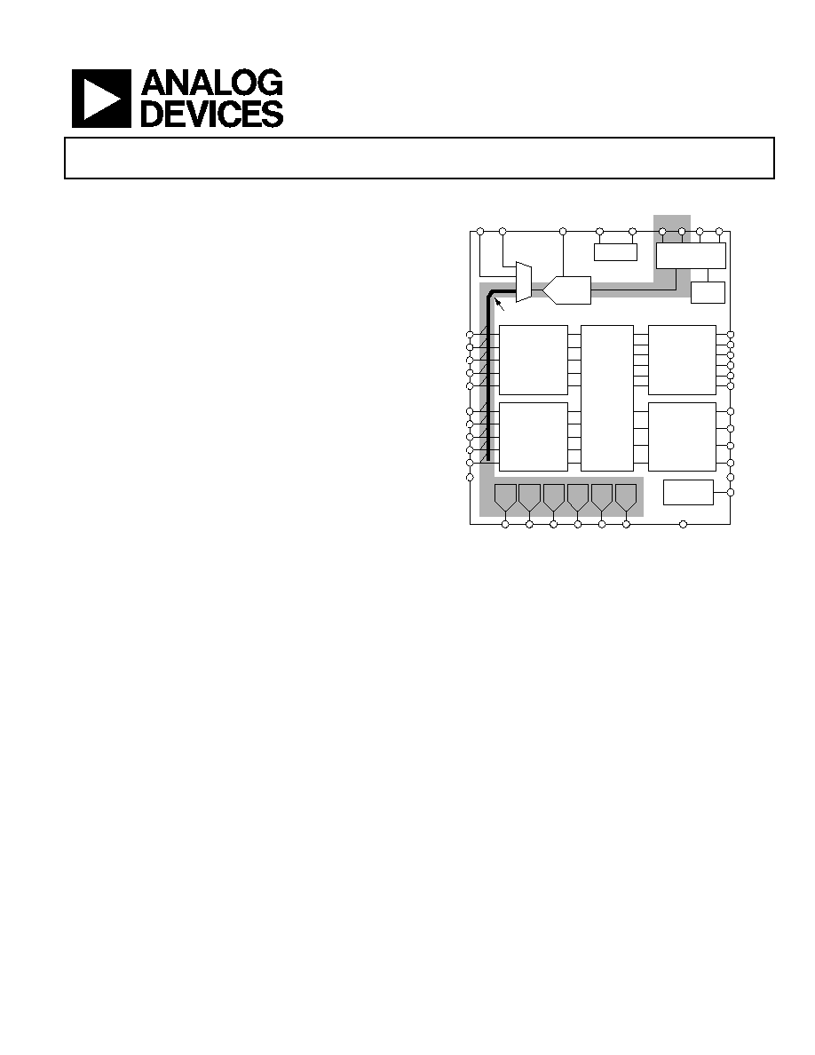
FUNCTIONAL BLOCK DIAGRAM
04609-
001
PDO7
PDO8
PDO9
PDO10
PDOGND
VDDCAP
VDD
ARBITRATOR
DAC1
V
OUT
DAC
DAC2
V
OUT
DAC
DAC3
V
OUT
DAC
DAC4
V
OUT
DAC
DAC5
V
OUT
DAC
DAC6
V
OUT
DAC
GND
VX1
VX2
VX3
VX4
VX5
VP1
VP2
VP3
VP4
VH
AGND
PROGRAMMABLE
RESET
GENERATORS
(SFDs)
DUAL-
FUNCTION
INPUTS
(LOGIC INPUTS
OR
SFDs)
SEQUENCING
ENGINE
CONFIGURABLE
OUTPUT
DRIVERS
(HV CAPABLE
OF DRIVING
GATES OF
N-CHANNEL FET)
CONFIGURABLE
OUTPUT
DRIVERS
(LV CAPABLE
OF DRIVING
LOGIC SIGNALS)
PDO1
PDO2
PDO3
PDO4
PDO5
PDO6
SDA SCL A1
A0
SMBus
INTERFACE
REFOUT
REFIN
AUX2
AUX1
REFGND
VREF
12-BIT
SAR ADC
MU
X
EEPROM
CLOSED-LOOP
MARGINING SYSTEM
ADM1066
Figure 1.
APPLICATIONS
Central office systems
Servers/routers
Multivoltage system line cards
DSP/FPGA supply sequencing
In-circuit testing of margined supplies
GENERAL DESCRIPTION
The ADM1066 is a configurable supervisory/sequencing device
that offers a single-chip solution for supply monitoring and
sequencing in multiple supply systems. In addition to these
functions, the ADM1066 integrates a 12-bit ADC and six 8-bit
voltage output DACs. These circuits can be used to implement a
closed-loop margining system, which enables supply adjustment
by altering either the feedback node or reference of a dc/dc
converter using the DAC outputs.
(continued on Page 3)

ADM1066
Rev. 0 | Page 2 of 32
TABLE OF CONTENTS
General Description ......................................................................... 3
Specifications..................................................................................... 4
Pin Configurations and Function Descriptions ........................... 7
Absolute Maximum Ratings............................................................ 8
Thermal Characteristics .............................................................. 8
ESD Caution.................................................................................. 8
Typical Performance Characteristics ............................................. 9
Powering the ADM1066 ................................................................ 12
Inputs................................................................................................ 13
Supply Supervision..................................................................... 13
Programming the Supply Fault Detectors............................... 13
Input Comparator Hysteresis.................................................... 14
Input Glitch Filtering ................................................................. 14
Supply Supervision with VXn Inputs....................................... 14
VXn Pins as Digital Inputs........................................................ 15
Outputs ............................................................................................ 16
Supply Sequencing through Configurable Output Drivers .. 16
Sequencing Engine ......................................................................... 17
Overview...................................................................................... 17
Warnings...................................................................................... 17
SMBus Jump/Unconditional Jump .......................................... 17
Sequencing Engine Application Example ............................... 18
Sequence Detector...................................................................... 19
Monitoring Fault Detector ........................................................ 19
Timeout Detector ....................................................................... 19
Fault Reporting........................................................................... 19
Voltage Readback............................................................................ 20
Supply Supervision with the ADC ........................................... 20
Supply Margining ........................................................................... 21
Overview ..................................................................................... 21
Open-Loop Margining .............................................................. 21
Closed-Loop Supply Margining ............................................... 21
Writing to the DACs .................................................................. 22
Choosing the Size of the Attenuation Resistor....................... 22
DAC Limiting/Other Safety Features ...................................... 22
Applications Diagram .................................................................... 23
Communicating with the ADM1066 ........................................... 24
Configuration Download at Power-Up ................................... 24
Updating the Configuration ..................................................... 24
Updating the Sequencing Engine............................................. 25
Internal Registers........................................................................ 25
EEPROM ..................................................................................... 25
Serial Bus Interface..................................................................... 25
Write Operations ........................................................................ 27
Read Operations ......................................................................... 29
Outline Dimensions ....................................................................... 31
Ordering Guide .......................................................................... 31
REVISION HISTORY
10/04--Revision 0: Initial Version

ADM1066
Rev. 0 | Page 3 of 32
GENERAL DESCRIPTION
(continued from Page 1)
Supply margining can be performed with a minimum of
external components. The margining loop can be used for in-
circuit testing of a board during production (for example, to
verify the board's functionality at -5% of nominal supplies),
or can be used dynamically to accurately control the output
voltage of a dc/dc converter.
The device also provides up to ten programmable inputs for
monitoring under, over, or out-of-window faults on up to ten
supplies. In addition, ten programmable outputs can be used as
logic enables. Six of them can also provide up to a 12 V output
for driving the gate of an N-channel FET, which can be placed
in the path of a supply.
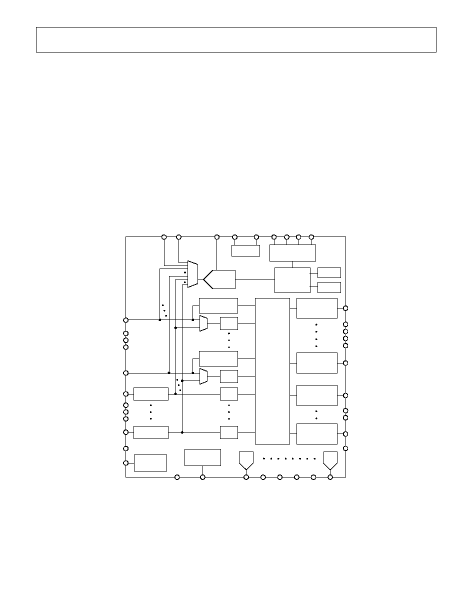
The logical core of the device is a sequencing engine. This state-
machine-based construction provides up to 63 different states.
This design enables very flexible sequencing of the outputs,
based on the condition of the inputs.
The device is controlled via configuration data that can be
programmed into an EEPROM. The whole configuration can
be programmed using an intuitive GUI-based software package
provided by ADI.
04609-002
GPI SIGNAL
CONDITIONING
SFD
GPI SIGNAL
CONDITIONING
SFD
SFD
SFD
SELECTABLE
ATTENUATOR
SELECTABLE
ATTENUATOR
DEVICE
CONTROLLER
OSC
EEPROM
SDA SCL A1
A0
SMBus
INTERFACE
REFOUT
REFIN
AUX1
AUX2
REFGND
VREF
12-BIT
SAR ADC
ADM1066
CONFIGURABLE
O/P DRIVER
(HV)
PDO1
PDO2
PDOGND
PDO3
DAC1
V
OUT
DAC
DAC6
V
OUT
DAC
VCCP
GND
DAC2 DAC3 DAC4 DAC5
PDO4
PDO5
PDO8
PDO9
CONFIGURABLE
O/P DRIVER
(HV)
PDO6
CONFIGURABLE
O/P DRIVER
(LV)
PDO7
CONFIGURABLE
O/P DRIVER
(LV)
PDO10
SEQUENCING
ENGINE
VX2
VX3
VX4
VP2
VP3
VP4
VH
VP1
VX1
SFDGND
VX5
VDDCAP
VDD
ARBITRATOR
REG 5.25V
CHARGE PUMP
Figure 2. Detailed Block Diagram

ADM1066
Rev. 0 | Page 4 of 32
SPECIFICATIONS
VH = 3.0 V to 14.4 V
1
, VPn = 3.0 V to 6.0 V
1
, T
A
= -40∞C to +85∞C, unless otherwise noted.
Table 1.
Parameter Min
Typ
Max
Unit
Test
Conditions/Comments
POWER
SUPPLY
ARBITRATION
VH, VPn
3.0
V
Minimum supply required on one of VPn, VH
VP
6.0
V
Maximum VDDCAP = 5.1 V, typical
VH
14.4
V
VDDCAP = 4.75 V
VDDCAP 2.7
4.75
5.4
V
Regulated
LDO
output
C
VDDCAP
10
µF
Minimum recommended decoupling capacitance
POWER
SUPPLY
Supply Current, I
VH
, I
VPn
4.2
6
mA
VDDCAP = 4.75 V, PDO1≠10 off, DACs off, ADC off
Additional
Currents
All PDO FET Drivers On
1
mA
VDDCAP = 4.75 V, PDO1-6 loaded with 1 µA each,
PDO7≠10 off
Current Available from VDDCAP
2
mA
Maximum additional load that can be drawn from
all PDO pull-ups to VDDCAP
DACs Supply Current
2.2
mA
6 DACs on with 100 µA maximum load on each
ADC Supply Current
1
mA
Running round-robin loop
EEPROM Erase Current
10
mA
1 ms duration only, VDDCAP = 3 V
SUPPLY FAULT DETECTORS
VH
Pin
Input Attenuator Error
±0.05
%
Midrange and high range
Detection
Ranges
High Range
6
14.4
V
Midrange 2.5
6
V
VPn
Pins
Input Attenuator Error
±0.05
%
Low range and midrange
Detection
Ranges
Midrange 2.5
6
V
Low Range
1.25
3
V
Ultralow Range
0.573
1.375
V
No input attenuation error
VX
Pins
Input
Impedance
1 M
Detection
Ranges
Ultralow Range
0.573
1.375
V
No input attenuation error
Absolute Accuracy
±1
%
VREF error + DAC nonlinearity + comparator offset
error + input attenuation error
Threshold Resolution
8
Bits
Digital Glitch Filter
0
µs
Minimum programmable filter length
100
µs
Maximum programmable filter length
ANALOG-TO-DIGITAL
CONVERTER
Signal Range
0
V
REFIN
V
The ADC can convert signals presented to the VH,
VPn, and VX_GPIn pins. VPn and VH input signals
are attenuated depending on selected range. A
signal at the pin corresponding to the selected
range is from 0.573 V to 1.375 V at the ADC input.
Input Reference Voltage on REFIN Pin,
V
REFIN
2.048
V
Resolution
12
Bits
INL
±2.5
LSB
Endpoint corrected, V
REFIN
= 2.048 V
Gain Error
±0.05
%
V
REFIN
= 2.048 V

ADM1066
Rev. 0 | Page 5 of 32
Parameter Min
Typ
Max
Unit
Test
Conditions/Comments
Conversion Time
0.44
ms
One conversion on one channel
84
ms
All 12 channels selected, 16x averaging enabled
Offset Error
±2
LSB
V
REFIN
= 2.048 V
Input Noise
0.25
LSB
rms
Direct input (no attenuator)
BUFFERED VOLTAGE OUTPUT DACs
Resolution
8
Bits
Code 0x80 Output Voltage
6 DACs are individually selectable for centering on
one of four output voltage ranges
Range 1
0.592
0.6
0.603
V
Range 2
0.796
0.8
0.803
V
Range 3
0.996
1
1.003
V
Range 4
1.246
1.25
1.253
V
Output Voltage Range
601.25
mV
Same range, independent of center point
LSB Step Size
2.36
mV
INL
±0.75
LSB
Endpoint
corrected
DNL
±0.4
LSB
Gain Error
1
%
Load Regulation
-4
mV
Sourcing Current, I
REFOUTMA X
= -200µA
2
mV
Sinking Current, I
REFOUTMA X
= 100µA
Maximum Load Capacitance
50
pF
Settling Time into 50 pF Load
2
µs
Load Regulation
2.5
mV
Per mA
PSRR
60
dB
DC
40
dB
100 mV step in 20 ns with 50 pF load
REFERENCE
OUTPUT
Reference Output Voltage
2.043
2.048
2.053
V
No load
Load Regulation
-0.25
mV
Sourcing current, I
DACnMAX
= -100 µA
0.25
mV
Sinking current, I
DACnMAX
= 100 µA
Minimum
Load
Capacitance
1 µF
Capacitor required for decoupling, stability
Load Regulation
2
mV
Per 100 µA
PSRR
60
dB
DC
PROGRAMMABLE DRIVER OUTPUTS
High Voltage (Charge Pump) Mode (PDO1≠6)
Output Impedance
500
k
V
OH
11 12.5
14
V
I
OH
= 0
10.5
12
13.5
V
I
OH
= 1µA
I
OUTAVG
20
µA
2 V < V
OH
< 7 V
Standard (Digital Output) Mode (PDO1≠10)
V
OH
2.4 V
V
PU
(pull-up to VDDCAP or V
PN
) = 2.7 V, I
OH
= 0.5 mA
4.5
V
V
PU
to V
pn
= 6.0 V, I
OH
= 0 mA
V
PU
- 0.3
V
V
PU
2.7 V, I
OH
= 0.5 mA
V
OL
0
0.50
V
I
OL
= 20 mA
I
OL
2
20
mA
Maximum sink current per PDO pin
I
SINK
2
60
mA
Maximum total sink for all PDOs
R
PULL-UP
20
k
Internal
pull-up
I
SOURCE
(VPn)
2
2
mA
Current load on any VPn pull-ups, that is, total
source current available through any number of
PDO pull-up switches configured onto any one
Three-State Output Leakage Current
10
µA
V
PDO
= 14.4 V
Oscillator
Frequency
90
100 110 kHz All
on-chip time delays derived from this clock

ADM1066
Rev. 0 | Page 6 of 32
Parameter Min
Typ
Max
Unit
Test
Conditions/Comments
DIGITAL INPUTS (VXn, A0, A1)
Input High Voltage, V
IH
2.0 V
Maximum
V
IN
= 5.5 V
Input Low Voltage, V
IL
0.8
V
Maximum
V
IN
= 5.5 V
Input High Current, I
IH
-1 µA
V
IN
= 5.5 V
Input Low Current, I
IL
1
µA
V
IN
= 0
Input Capacitance
5
pF
Programmable Pull-Down Current,
I
PULL-DOWN
20
µA
VDDCAP = 4.75, T
A
= 25∞C, if known logic state is
required
SERIAL BUS DIGITAL INPUTS (SDA, SCL)
Input High Voltage, V
IH
2.0 V
Input Low Voltage, V
IL
0.8
V
Output Low Voltage, V
OL
2
0.4
V
I
OUT
= -3.0 mA
SERIAL
BUS
TIMING
Clock Frequency, f
SCLK
400
kHz
Bus Free Time, t
BUF
4.7 µs
Start Setup Time, t
SU;STA
4.7 µs
Start Hold Time, t
HD;STA
4 µs
SCL Low Time, t
LOW
4.7 µs
SCL High Time, t
HIGH
4 µs
SCL, SDA Rise Time, t
r
1000
µs
SCL, SDA Fall Time, t
f
300
µs
Data Setup Time, t
SU;DAT
250
ns
Data Hold Time, t
HD;DAT
5 ns
Input Low Current, I
IL
1
µA
V
IN
= 0
SEQUENCING
ENGINE
TIMING
State Change Time
10
µs
1
At least one of the VH, VP1-4 pins must be
3.0 V to maintain the device supply on VDDCAP.
2
Specification is not production tested, but is supported by characterization data at initial product release.

ADM1066
Rev. 0 | Page 7 of 32
PIN CONFIGURATIONS AND FUNCTION DESCRIPTIONS
04609-003
ADM1066
TOP VIEW
(Not to Scale)
GND
40
V
DDCAP
39
AUX
1
38
AUX
2
37
SD
A
36
SC
L
35
A1
34
A0
33
V
CCP
32
PDOGND
31
AGND
11
RE
FGND
12
RE
FIN
13
RE
FOUT
14
DAC1
15
DAC2
16
DAC3
17
DAC4
18
DAC5
19
DAC6
20
VX1
1
VX2
2
VX3
3
VX4
4
VX5
5
VP1
6
VP2
7
VP3
8
VP4
9
VH
10
PDO1
30
PDO2
29
PDO3
28
PDO4
27
PDO5
26
PDO6
25
PDO7
24
PDO8
23
PDO9
22
PDO10
21
PIN 1
INDICATOR
Figure 3. LFCSP Pin Configuration
04609-004
NC = NO CONNECT
NC
48
GND
47
V
D
DCAP
46
AUX
1
45
AUX
2
44
SD
A
43
SC
L
42
A1
41
A0
40
VC
C
P
39
PDOGND
38
NC
37
NC
13
AGND
14
RE
FGND
15
RE
FIN
16
RE
FOUT
17
DAC1
18
DAC2
19
DAC3
20
DAC4
21
DAC5
22
DAC6
23
NC
24
NC
1
VX1
2
VX2
3
VX3
4
VX4
5
VX5
6
VP1
7
VP2
8
VP3
9
VP4
10
VH
11
NC
12
NC
36
PDO1
35
PDO2
34
PDO3
33
PDO4
32
PDO5
31
PDO6
30
PDO7
29
PDO8
28
PDO9
27
PDO10
26
NC
25
ADM1066
TOP VIEW
(Not to Scale)
PIN 1
INDICATOR
Figure 4. TQFP Pin Configuration
Table 2. Pin Function Descriptions
Pin No.
LFCSP TQFP
Mnemonic Description
1, 12≠13,
24≠25,
36≠37, 48
NC
No connection.
1≠5 2≠6
VX1≠5 High Impedance Inputs to Supply Fault Detectors. Fault thresholds can be set from 0.573 V to 1.375 V.
Alternatively, these pins can be used as general-purpose digital inputs.
6≠9 7≠10
VP1≠4
Low Voltage Inputs to Supply Fault Detectors. Three input ranges can be set by altering the input
attenuation on a potential divider connected to these pins, the output of which connects to a supply
fault detector. These pins allow thresholds from 2.5 V to 6.0 V, 1.25 V to 3.00 V, and 0.573 V to 1.375 V.
10 11
VH
High Voltage Input to Supply Fault Detectors. Three input ranges can be set by altering the input
attenuation on a potential divider connected to this pin, the output of which connects to a supply
fault detector. This pin allows thresholds from 6.0 V to 14.4 V and 2.5 V to 6.0 V.
11
14
AGND
Ground Return for Input Attenuators.
12
15
REFGND
Ground Return for On-Chip Reference Circuits.
13
16
REFIN
Reference Input for ADC. Nominally, 2.048 V.
14
17
REFOUT
2.048 V Reference Output.
15≠20
18≠23
DAC1≠6
Voltage Output DACs. These pins default to high impedance at power-up.
21≠30 26≠35
PDO10≠1 Programmable
Output
Drivers.
31
38
PDOGND
Ground Return for Output Drivers.
32 39
VCCP Central Charge-Pump Voltage of 5.25 V. A reservoir capacitor must be connected between this pin
and GND.
33
40
A0
Logic Input. This pin sets the seventh bit of the SMBus interface address.
34
41
A1
Logic Input. This pin sets the sixth bit of the SMBus interface address.
35
42
SCL
SMBus Clock Pin. Open-drain output requires external resistive pull-up.
36
43
SDA
SMBus Data I/O Pin. Open-drain output requires external resistive pull-up.
37
44
AUX2
Auxiliary, Single-Ended ADC Input.
38
45
AUX1
Auxiliary, Single-Ended ADC Input.
39
46
VDDCAP
Device Supply Voltage. Linearly regulated from the highest of the VP1≠4, VH pins to a typical of 4.75 V.
40 47
GND
Supply
Ground.

ADM1066
Rev. 0 | Page 8 of 32
ABSOLUTE MAXIMUM RATINGS
Table 3.
Parameter Rating
Voltage on VH Pin
16 V
Voltage on VP Pins
7 V
Voltage on VX Pins
-0.3 V to +6.5 V
Voltage on AUX1, AUX2, REFIN Pins
-0.3 V to +5 V
Input Current at Any Pin
±5 mA
Package Input Current
±20 mA
Maximum Junction Temperature (T
J
max)
150∞C
Storage Temperature Range
-65∞C to +150∞C
Lead Temperature, Soldering
Vapor Phase, 60 s
215∞C
Stresses above those listed under Absolute Maximum Ratings
may cause permanent damage to the device. This is a stress
rating only; functional operation of the device at these or any
other conditions above those indicated in the operational
section of this specification is not implied. Exposure to absolute
maximum rating conditions for extended periods may affect
device reliability.
THERMAL CHARACTERISTICS
40-lead LFCSP package:
JA
= 25∞C/W
48-lead TQFP package:
JA
= 14.8∞C/W
ESD CAUTION
ESD (electrostatic discharge) sensitive device. Electrostatic charges as high as 4000 V readily accumulate on
the human body and test equipment and can discharge without detection. Although this product features
proprietary ESD protection circuitry, permanent damage may occur on devices subjected to high energy
electrostatic discharges. Therefore, proper ESD precautions are recommended to avoid performance
degradation or loss of functionality.

ADM1066
Rev. 0 | Page 9 of 32
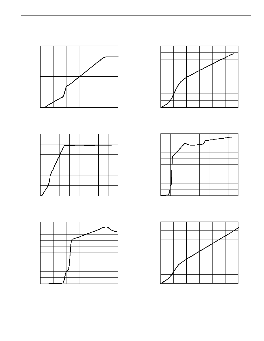
TYPICAL PERFORMANCE CHARACTERISTICS
6
0
1
2
3
4
5
0
6
5
4
3
2
1
04609-050
V
VP1
(V)
V
VDDCAP
(V
)
Figure 5. V
VDDCAP
vs. V
VP1
6
0
1
2
3
4
5
0
16
14
12
10
8
6
4
2
04609-051
V
VH
(V)
V
V
DDCAP
(V
)
Figure 6. V
VDDCAP
vs. V
VH
5.0
4.5
4.0
3.5
3.0
2.5
2.0
1.5
1.0
0.5
0
0
1
2
3
4
5
6
04609-052
V
VP1
(V)
I
VP1
(mA)
Figure 7. I
VP1
vs. V
VP1
(VP1 as Supply)
180
160
140
120
100
80
60
40
20
0
0
1
2
3
4
5
6
04609-053
V
VP1
(V)
I
VP1
(
µ
A)
Figure 8. I
VP1
vs. V
VP1
(VP1 Not as Supply)
5.0
4.5
4.0
3.5
3.0
2.5
2.0
1.5
1.0
0.5
0
0
16
14
12
10
8
6
4
2
04609-054
V
VH
(V)
I
VH
(mA)
Figure 9. I
VH
vs. V
VH
(VH as Supply)
350
300
250
200
150
100
50
0
0
6
5
4
3
2
1
04609-055
V
VH
(V)
I
VH
(
µ
A)
Figure 10. I
VH
vs. V
VH
(VH Not as Supply)

ADM1066
Rev. 0 | Page 10 of 32
14
12
10
8
6
4
2
0
0
15.0
12.5
10.0
7.5
5.0
2.5
04609-056
I
LOAD
CURRENT (
µ
A)
V
PDO
1
CHARGE
P
U
MP
E
D
Figure 11. V
PDO1
(FET Drive Mode) vs. I
LOAD
5.0
4.5
4.0
3.5
3.0
2.5
2.0
1.5
1.0
0.5
0
0
6
5
4
3
2
1
04609-057
I
LOAD
(mA)
V
PD
O1
(V
)
VP1 = 5V
VP1 = 3V
Figure 12. V
PDO1
(Strong Pull-Up VP) vs. I
LOAD
4.5
4.0
3.5
3.0
2.5
2.0
1.5
1.0
0.5
0
0
60
50
40
30
20
10
04609-058
I
LOAD
(
µ
A)
V
PDO
1
(V
)
VP1 = 5V
VP1 = 3V
Figure 13. V
PDO1
(Weak Pull-Up to VP) vs. I
LOAD
1.0
≠1.0
≠0.8
≠0.6
≠0.4
≠0.2
0
0.2
0.4
0.6
0.8
4000
1000
2000
3000
0
04609-066
CODE
DNL (LS
B
)
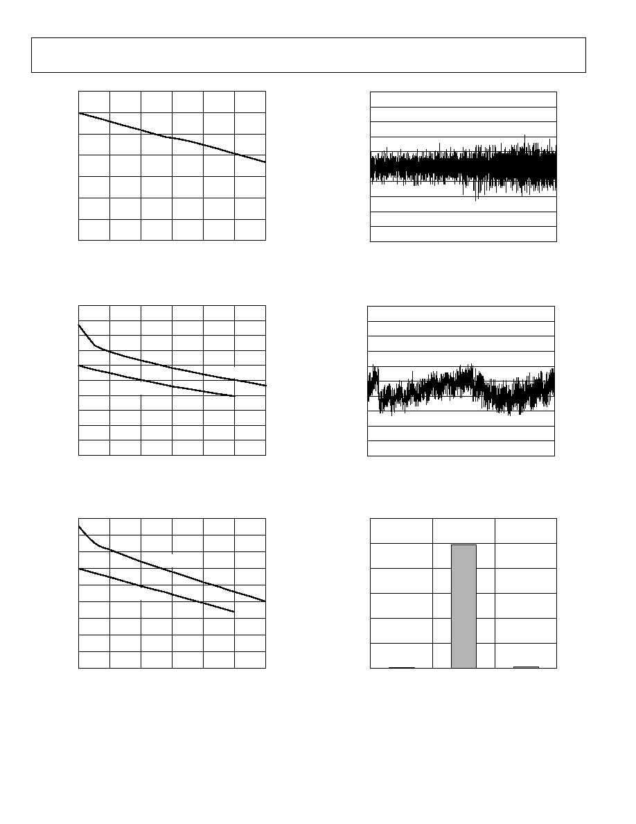
Figure 14. DNL for ADC
1.0
≠1.0
≠0.8
≠0.6
≠0.4
≠0.2
0
0.2
0.4
0.6
0.8
0
4000
3000
2000
1000
04609-063
CODE
INL (LSB)
Figure 15. INL for ADC
12000
10000
8000
6000
4000
2000
0
2049
2048
2047
04609-064
CODE
HITS
P
E
R
CODE
81
9894
25
Figure 16. ADC Noise, Midcode Input, 10,000 Reads

ADM1066
Rev. 0 | Page 11 of 32
04609-
059
CH1
200mV
M1.00
µ
s
CH1 756mV
1
DAC
BUFFER
OUTPUT
PROBE
POINT
47pF
20k
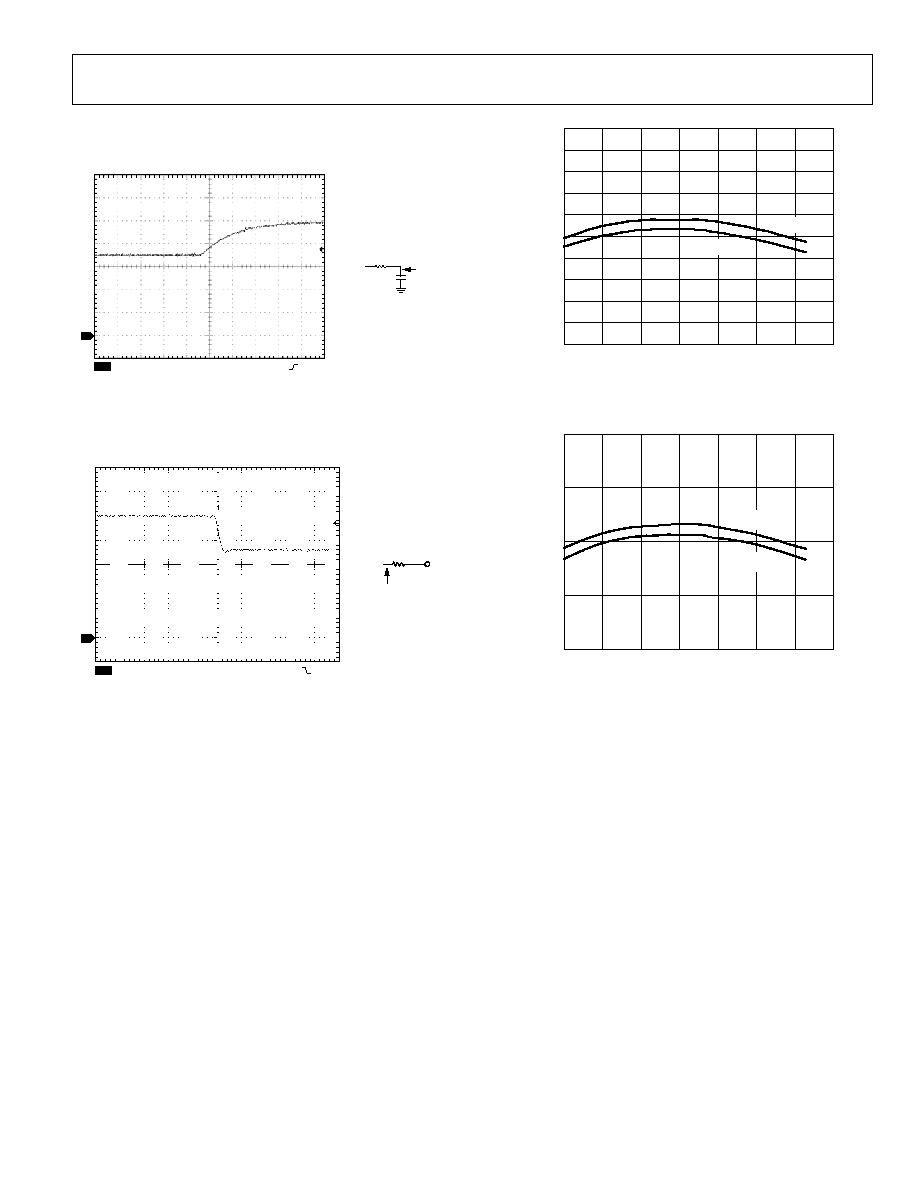
Figure 17. Transient Response of DAC Code Change into Typical Load
04609-
060
CH1
200mV
M1.00
µ
s
CH1 944mV
1
DAC
BUFFER
OUTPUT
1V
PROBE
POINT
100k
Figure 18. Transient Response of DAC to Turn-On from HI-Z State
1.005
1.004
1.003
1.002
1.001
1.000
0.999
0.998
0.997
0.996
0.995
≠40
≠20
0
20
40
60
100
80
04609-065
TEMPERATURE (
∞
C)
DAC OUTP
UT
VP1 = 3.0V
VP1 = 4.75V
Figure 19. DAC Output vs. Temperature
2.058
2.038
2.043
2.048
2.053
≠40
≠20
0
20
40
60
100
80
04609-061
TEMPERATURE (
∞
C)
RE
FOUT (V
)
VP1 = 3.0V
VP1 = 4.75V
Figure 20. REFOUT vs. Temperature

ADM1066
Rev. 0 | Page 12 of 32
POWERING THE ADM1066
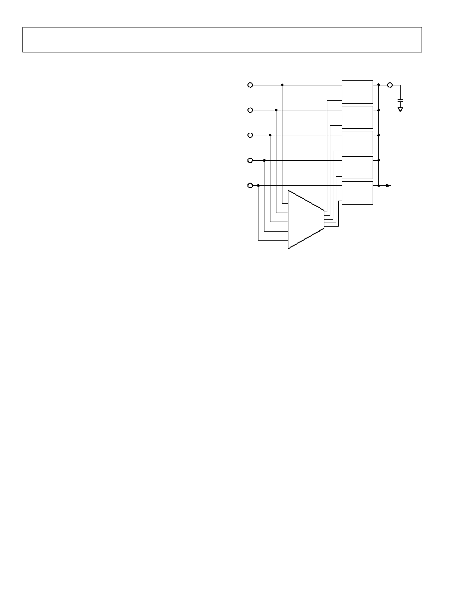
The ADM1066 is powered from the highest voltage input on
either the positive-only supply inputs (VPn) or the high voltage
supply input (VH). This technique offers improved redundancy
as the device is not dependent on any particular voltage rail to
keep it operational. The same pins are used for supply fault
detection (discussed later in the next section). A VDD arbitrator
on the device chooses which supply to use. The arbitrator can
be considered an OR'ing of five LDOs together. A supply
comparator chooses which of the inputs is highest and selects
this one to provide the on-chip supply. There is minimal
switching loss with this architecture (~0.2 V), resulting in the
ability to power the ADM1066 from a supply as low as 3.0 V.
Note that the supply on the VXn pins cannot be used to power
the device.
An external capacitor to GND is required to decouple the on-
chip supply from noise. This capacitor should be connected to
the VDDCAP pin, as shown in Figure 21. The capacitor has
another use during brownouts (momentary loss of power).
Under these conditions, when the input supply (VPn or VH)
dips transiently below V
DD
, the synchronous rectifier switch
immediately turns off so that it does not pull V
DD
down. The
V
DD
cap can then act as a reservoir to keep the device active
until the next highest supply takes over the powering of the
device. 10 µF is recommended for this reservoir/decoupling
function.
Note that when two or more supplies are within 100 mV of each
other, the supply that takes control of V
DD
first keeps control.
For example, if VP1 is connected to a 3.3 V supply, then V
DD
powers up to approximately 3.1 V through VP1. If VP2 is then
connected to another 3.3 V supply, VP1 still powers the device,
unless VP2 goes 100 mV higher than VP1.
SUPPLY
COMPARATOR
IN
EN
OUT
4.75V
LDO
IN
EN
OUT
4.75V
LDO
IN
EN
OUT
4.75V
LDO
IN
EN
OUT
4.75V
LDO
IN
EN
OUT
4.75V
LDO
VH
VP4
VP3
VP2
VP1
VDDCAP
INTERNAL
DEVICE
SUPPLY
0
4609-022
Figure 21. VDD Arbitrator Operation

ADM1066
Rev. 0 | Page 13 of 32
INPUTS
SUPPLY SUPERVISION
The ADM1066 has ten programmable inputs. Five of these are
dedicated supply fault detectors (SFDs). These dedicated inputs
are called VH and VP1≠4 by default. The other five inputs are
labeled VX1≠VX5 and have dual functionality. They can be
used as either supply fault detectors, with similar functionality
to VH and VP1≠4, or CMOS/TTL-compatible logic inputs to
the devices. Therefore, the ADM1066 can have up to ten analog
inputs, a minimum of five analog inputs and five digital inputs,
or a combination. If an input is used as an analog input, it
cannot be used as a digital input. Therefore, a configuration
requiring ten analog inputs has no digital inputs available.
Table 5 shows the details of each of the inputs.
04609-
023
+
≠
+
≠
UV
COMPARATOR
VREF
FAULT TYPE
SELECT
OV
COMPARATOR
FAULT
OUTPUT
GLITCH
FILTER
VPn
MID
LOW
RANGE
SELECT
ULTRA
LOW
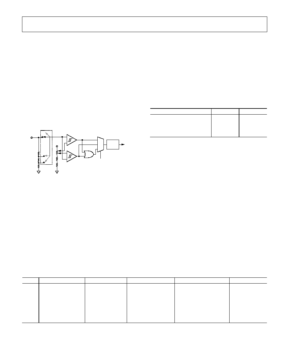
Figure 22. Supply Fault Detector Block
PROGRAMMING THE SUPPLY FAULT DETECTORS
The ADM1066 has up to ten supply fault detectors (SFDs) on its
ten input channels. These highly programmable reset generators
enable the supervision of up to ten supply voltages. The supplies
can be as low as 0.573 V and as high as 14.4 V. The inputs can be
configured to detect an undervoltage fault (the input voltage
droops below a preprogrammed value), an overvoltage fault (the
input voltage rises above a preprogrammed value) or an out-of-
window fault (undervoltage or overvoltage). The thresholds can
be programmed to an 8-bit resolution in registers provided in
the ADM1066. This translates to a voltage resolution that is
dependent on the range selected.
The resolution is given by
Step Size = Threshold Range/255
Therefore, if the high range is selected on VH, the step size can
be calculated as follows:
(14.4 V - 4.8 V)/255 = 37.6 mV
Table 4 lists the upper and lower limit of each available range,
the bottom of each range (V
B
), and the range itself (V
R
).
Table 4. Voltage Range Limits
Voltage Range (V)
V
B
(V)
V
R
(V)
0.573 to 1.375
0.573
0.802
1.25 to 3.00
1.25
1.75
2.5 to 6.0
2.5
3.5
4.8 to 14.4
4.8
9.6
The threshold value required is given by
V
T
= (V
R
◊ N)/255 + V
B
where:
V
T
is the desired threshold voltage (UV or OV).
V
R
is the voltage range.
N is the decimal value of the 8-bit code.
V
B
is the bottom of the range.
Reversing the equation, the code for a desired threshold is given
by
N = 255 ◊ (V
T
- V
B
)/V
R
For example, if the user wants to set a 5 V OV threshold on VP1,
the code to be programmed in the PS1OVTH register
(discussed in the AN-698 application note) is given by
N = 255 ◊ (5 - 2.5)/3.5
Therefore, N = 182 (1011 0110 or 0xB6).
Table 5. Input Functions, Thresholds, and Ranges
Input
Function
Voltage Range (V)
Maximum Hysteresis
Voltage Resolution (mV)
Glitch Filter (µs)
VH
High V Analog Input
2.5≠6.0
425 mV
13.7
0≠100
4.8≠14.4
1.16
V
37.6
0≠100
VPn
Positive Analog Input
0.573≠1.375
97.5 mV
3.14
0≠100
1.25≠3.00
212
mV
6.8
0≠100
2.5≠6.0
425 mV
13.7
0≠100
VXn
High Z Analog Input
0.573≠1.375
97.5 mV
3.14
0≠100
Digital
Input
0≠5
N/A
N/A
0≠100

ADM1066
Rev. 0 | Page 14 of 32
INPUT COMPARATOR HYSTERESIS
The UV and OV comparators shown in Figure 22 are always
looking at VPn. To avoid chattering (multiple transitions when
the input is very close to the set threshold level), these compara-
tors have digitally programmable hysteresis. The hysteresis can
be programmed up to the values shown in Table 5.
The hysteresis is added after a supply voltage goes out of
tolerance. Therefore, the user can program how much above
the UV threshold the input must rise again before a UV fault is
deasserted. Similarly, the user can program how much below the
OV threshold an input must fall again before an OV fault is
deasserted.
The hysteresis figure is given by
V
HYST
= V
R
◊ N
THRESH
/255
where:
V
HYST
is the desired hysteresis voltage.
N
THRESH
is the decimal value of the 5-bit hysteresis code.
Note that N
THRESH
has a maximum value of 31. The maximum
hysteresis for the ranges is listed in Table 5.
INPUT GLITCH FILTERING
The final stage of the SFDs is a glitch filter. This block provides
time-domain filtering on the output of the SFD comparators.
This allows the user to remove any spurious transitions such as
supply bounce at turn-on. The glitch filter function is additional
to the digitally programmable hysteresis of the SFD compara-
tors. The glitch filter timeout is programmable up to 100 µs.
For example, when the glitch filter timeout is 100 µs, any pulses
appearing on the input of the glitch filter block that are less than
100 µs in duration are prevented from appearing on the output
of the glitch filter block. Any input pulse that is longer than
100 µs does appear on the output of the glitch filter block. The
output is delayed with respect to the input by 100 µs. The
filtering process is shown in Figure 23.
04609-024
T
0
T
GF
T
0
T
GF
T
0
T
GF
T
0
T
GF
INPUT
INPUT PULSE SHORTER
THAN GLITCH FILTER TIMEOUT
INPUT PULSE LONGER
THAN GLITCH FILTER TIMEOUT
OUTPUT
PROGRAMMED
TIMEOUT
PROGRAMMED
TIMEOUT
INPUT
OUTPUT
Figure 23. Input Glitch Filter Function
SUPPLY SUPERVISION WITH VXn INPUTS
The VXn inputs have two functions. They can be used as either
supply fault detectors or digital logic inputs. When selected as an
analog (SFD) input, the VXn pins have very similar functionality
to the VH and VPn pins. The major difference is that the VXn
pins have only one input range: 0.573 V to 1.375 V. Therefore,
these inputs can directly supervise only the very low supplies.
However, the input impedance of the VXn pins is high, allowing
an external resistor divide network to be connected to the pin.
Thus, any supply can be potentially divided down into the input
range of the VXn pin and supervised. This enables the ADM1066
to monitor other supplies such as +24 V, +48 V, and -5 V.
An additional supply supervision function is available when the
VXn pins are selected as digital inputs. In this case, the analog
function is available as a second detector on each of the dedi-
cated analog inputs, VP1≠4 and VH. The analog function of
VX1 is mapped to VP1, VX2 is mapped to VP2, and so on. VX5
is mapped to VH. In this case, these SFDs can be viewed as a
secondary or warning SFD.
The secondary SFDs are fixed to the same input range as the
primary SFD. They are used to indicate warning levels rather
than failure levels. This allows faults and warnings to be gener-
ated on a single supply using only one pin. For example, if VP1
is set to output a fault if a 3.3 V supply droops to 3.0 V, VX1 can
be set to output a warning at 3.1 V. Warning outputs are available
for readback from the status registers. They are also OR'ed
together and fed into the sequencing engine (SE), allowing
warnings to generate interrupts on the PDOs. Therefore, in the
example above, if the supply droops to 3.1 V, a warning is
generated, and remedial action can be taken before the supply
drops out of tolerance.

ADM1066
Rev. 0 | Page 15 of 32
VXn PINS AS DIGITAL INPUTS
As mentioned previously, the VXn input pins on the ADM1066
have dual functionality. The second function is as a digital input
to the device. Therefore, the ADM1066 can be configured for up
to five digital inputs. These inputs are TTL/CMOS-compatible.
Standard logic signals can be applied to the pins: RESET from
reset generators, PWRGOOD signals, fault flags, manual resets,
and so on. These signals are available as inputs to the SE, and so
can be used to control the status of the PDOs. The inputs can be
configured to detect either a change in level or an edge.
When configured for level detection, the output of the digital
block is a buffered version of the input. When configured for
edge detection, once the logic transition is detected, a pulse of
programmable width is output from the digital block. The width
is programmable from 0 µs to 100 µs.
The digital blocks feature the same glitch filter function that is
available on the SFDs. This enables the user to ignore spurious
transitions on the inputs. For example, the filter can be used to
debounce a manual reset switch.
When configured as digital inputs, each of the VXn pins has a
weak (10 µA) pull-down current source available for placing the
input in a known condition, even if left floating. The current
source, if selected, weakly pulls the input to GND.
04609-027
DETECTOR
VXn
(DIGITAL INPUT)
GLITCH
FILTER
VREF = 1.4V
TO
SEQUENCING
ENGINE
+
≠
Figure 24. VXn Digital Input Function

ADM1066
Rev. 0 | Page 16 of 32
OUTPUTS
SUPPLY SEQUENCING THROUGH
CONFIGURABLE OUTPUT DRIVERS
Supply sequencing is achieved with the ADM1066 using the
programmable driver outputs (PDOs) on the device as control
signals for supplies. The output drivers can be used as logic
enables or as FET drivers.
The sequence in which the PDOs are asserted (and, therefore,
the supplies are turned on) is controlled by the sequencing
engine (SE). The SE determines what action is to be taken with
the PDOs based on the condition of the inputs of the ADM1066.
Therefore, the PDOs can be set up to assert when the SFDs are
in tolerance, the correct input signals are received on the VXn
digital pins, no warnings are received from any of the inputs of
the device, and so on. The PDOs can be used for a variety of
functions. The primary function is to provide enable signals for
LDOs or dc/dc converters, which generate supplies locally on a
board. The PDOs can also be used to provide a POWER_GOOD
signal when all the SFDs are in tolerance, or a RESET output if
one of the SFDs goes out of specification (this can be used as a
status signal for a DSP, FPGA, or other microcontroller).
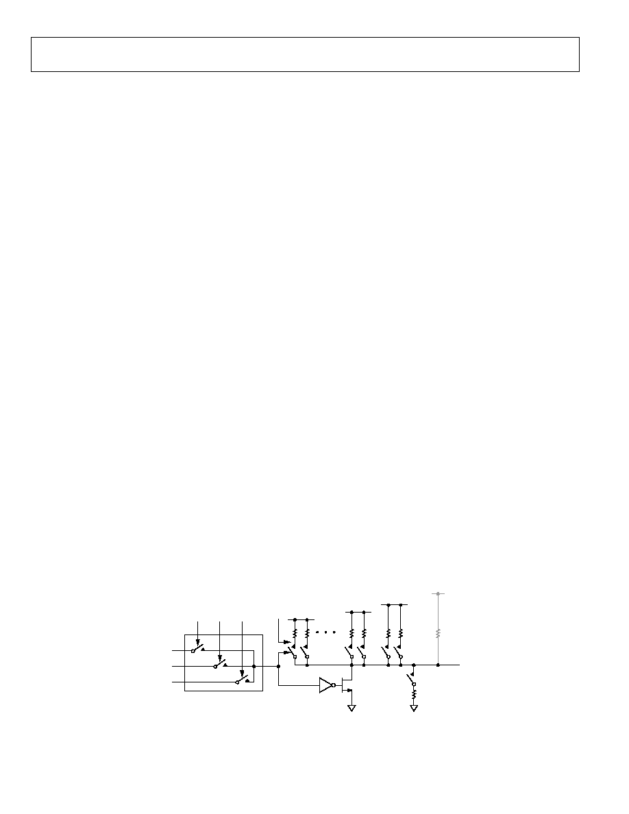
The PDOs can be programmed to pull up to a number of
different options. The outputs can be programmed as follows:
∑
Open-drain (allowing the user to connect an external pull-up
resistor)
∑
Open-drain with weak pull-up to V
DD
∑
Push/pull to V
DD
∑
Open-drain with weak pull-up to VPn
∑
Push/pull to VPn
∑
Strong pull-down to GND
∑
Internally charge-pumped high drive (12 V, PDO1≠6 only)
The last option (available only on PDO1≠6) allows the user to
directly drive a voltage high enough to fully enhance an external
N-FET, which is used to isolate, for example, a card-side voltage
from a backplane supply (a PDO can sustain greater than 10.5 V
into a 1 µA load). The pull-down switches can also be used to
drive status LEDs directly.
The data driving each of the PDOs can come from one of three
sources. The source can be enabled in the PnPDOCFG con-
figuration register (see the AN-698 application note for details).
The data sources are
∑
Output from the SE.
∑
Directly from the SMBus. A PDO can be configured so that
the SMBus has direct control over it. This enables software
control of the PDOs. Therefore, a microcontroller can be
used to initiate a software power-up/power-down sequence.
∑
On-Chip Clock. A 100 kHz clock is generated on the device.
This clock can be made available on any of the PDOs. It can
be used, for example, to clock an external device such as
an LED.
By default, the PDOs are pulled to GND by a weak (20 k) on-
chip pull-down resistor. This is also the condition of the PDOs
on power-up, until the configuration is downloaded from
EEPROM and the programmed setup is latched. The outputs
are actively pulled low once a supply of 1 V or greater is on VPn
or VH. The outputs remain high impedance prior to 1 V appear-
ing on VPn or VH. This provides a known condition for the
PDOs during power-up. The internal pull-down can be over-
driven with an external pull-up of suitable value tied from the
PDO pin to the required pull-up voltage. The 20 k resistor
must be accounted for in calculating a suitable value. For
example, if PDOn must be pulled up to 3.3 V, and 5 V is available
as an external supply, the pull-up resistor value is given by
3.3 V = 5 V ◊ 20 k/(R
UP
+ 20 k)
Therefore,
R
UP
= (100 k - 66 k)/3.3 = 10 k
04609-028
PDO
SE DATA
CFG4 CFG5 CFG6
SMBus DATA
CLK DATA
10
20k
10
20k
VP1
SEL
VP4
10
20k
V
DD
VFET (PDO1-6 ONLY)
20k
Figure 25. Programmable Driver Output

ADM1066
Rev. 0 | Page 17 of 32
SEQUENCING ENGINE
OVERVIEW
The ADM1066's sequencing engine (SE) provides the user with
powerful and flexible control of sequencing. The SE implements
a state machine control of the PDO outputs, with state changes
conditional on input events. SE programs can enable complex
control of boards such as power-up and power-down sequence
control, fault event handling, interrupt generation on warnings,
and so on. A watchdog function that verifies the continued
operation of a processor clock can be integrated into the SE
program. The SE can also be controlled via the SMBus, giving
software or firmware control of the board sequencing.
The SE state machine comprises 63 state cells. Each state has the
following attributes:
∑
Monitors signals indicating the status of the 10 input pins,
VP1 to VP4, VH, and VX1 to VX5.
∑
Can be entered from any other state.
∑
Three exit routes move the state machine on to a next state:
sequence detection, fault monitoring, and timeout.
∑
Delay timers for the sequence and timeout blocks can be
programmed independently, and change with each state
change. The range of timeouts is from 0 ms to 400 ms.
∑
Output condition of the 10 PDO pins is defined and fixed
within a state.
∑
Transition from one state to the next is made in less than
20 µs, which is the time needed to download a state definition
from EEPROM to the SE.
04609-029
SEQUENCE
TIMEOUT
MONITOR
FAULT
STATE
Figure 26. State Cell
The ADM1066 offers up to 63 state definitions. The signals
monitored to indicate the status of the input pins are the
outputs of the SFDs.
WARNINGS
The SE also monitors warnings. These warnings can be
generated when the ADC readings violate their limit register
value or when the secondary voltage monitors on VP1≠4 and
VH. The warnings are all OR'ed together and are available as a
single warning input to each of the three blocks that enable
exiting from a state.
SMBus JUMP/UNCONDITIONAL JUMP
The SE can be forced to advance to the next state uncondition-
ally. This enables the user to force the SE to advance. Examples
of where this might be used include moving to a margining
state or debugging a sequence. The SMBus jump or go-to
command can be seen as another input to sequence and
timeout blocks, which provide an exit from each state.
Table 6. Sample Sequence State Entries
State Sequence
Timeout
Monitor
IDLE1
If VX1 is low , go to state IDLE2.
IDLE2
If VP1 is okay, go to state EN3V3.
EN3V3
If VP2 is okay, go to state EN2V5.
If VP2 is not okay after 10 ms, go to
state DIS3V3.
If VP1 is not okay, go to state IDLE1.
DIS3V3
If VX1 is high, go to state IDLE1.
EN2V5
If VP3 is okay, go to state PWRGD.
If VP3 is not okay after 20 ms, go to
state DIS2V5.
If VP1 or VP2 is not okay, go to state FSEL2.
DIS2V5
If VX1 is high, go to state IDLE1.
FSEL1
If VP3 is not okay, go to state DIS2V5.
If VP1 or VP2 is not okay, go to state FSEL2.
FSEL2
If VP2 is not okay, go to state DIS3V3.
If VP1 is not okay, go to state IDLE1.
PWRGD
If VX1 is high, go to state DIS2V5.
If VP1, VP2, or VP3 is not okay, go to state
FSEL1.

ADM1066
Rev. 0 | Page 18 of 32
SEQUENCING ENGINE APPLICATION EXAMPLE
The application in this section demonstrates the operation of
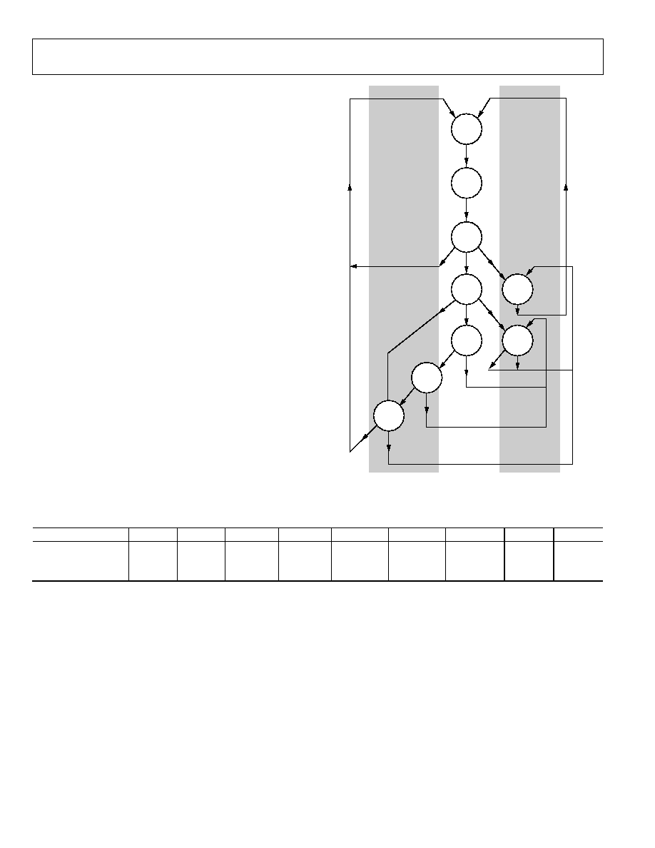
the SE. Figure 27 shows how the simple building block of a
single SE state can be used to build a power-up sequence for a
3-supply system.
Table 7 lists the PDO outputs for each state in the same SE
implementation. In this system, the presence of a good 5 V
supply on VP1 and the VX1 pin held low are the triggers required
for a power-up sequence to start. The sequence intends to turn
on the 3.3 V supply next, then the 2.5 V supply (assuming
successful turn-on of the 3.3 V supply). Once all three supplies
are good, the PWRGD state is entered, where the SE remains
until a fault occurs on one of the three supplies, or it is instructed
to go through a power-down sequence by VX1 going high.
Faults are dealt with throughout the power-up sequence on a
case-by-case basis. The following sections, which describe the
individual blocks, use this sample application to demonstrate
the state machine's actions.
04609-030
IDLE1
IDLE2
EN3V3
DIS3V3
DIS2V5
PWRGD
FSEL1
FSEL2
SEQUENCE
STATES
MONITOR FAULT
STATES
TIMEOUT
STATES
VX1 = 0
VP1 = 1
VP1 = 0
(VP1 + VP2) = 0
(VP1 + VP2 + VP3) = 0
(VP1 +
VP2) = 0
VP2 = 1
VP3 = 1
VP2 = 0
VX1 = 1
VP3 = 0
VP2 = 0
VP1 = 0
VX1 = 1
VX1 = 1
10ms
20ms
EN2V5
Figure 27. Sample Application Flow Diagram
Table 7. PDO Outputs for Each State
PDO
Outputs
IDLE1 IDLE2 EN3V3 EN2V5 DIS3V3 DIS2V5 PWRGD FSEL1 FSEL2
PDO1 = 3V3ON
0
0
1
1
0
1
1
1
1
PDO2 = 2V5ON
0
0
0
1
1
0
1
1
1
PDO3 = FAULT
0
0
0
0
1
1
0
1
1

ADM1066
Rev. 0 | Page 19 of 32
SEQUENCE DETECTOR
The sequence detector block is used to detect when a step in a
sequence has been completed. It looks for one of the inputs to
the SE to change state, and is most often used as the gate on
successful progress through a power-up or power-down
sequence. A timer block is included in this detector, which
can insert delays into a power-up or power-down sequence,
if required. Timer delays can be set from 10 µs to 400 ms.
Figure 28 is a block diagram of the sequence detector.
04609-032
SUPPLY FAULT
DETECTION
LOGIC INPUT CHANGE
OR FAULT DETECTION
WARNINGS
FORCE FLOW
(UNCONDITIONAL JUMP)
VP1
VX5
INVERT
SEQUENCE
DETECTOR
SELECT
TIMER
Figure 28. Sequence Detector Block Diagram
The sequence detector can also help to identify monitoring
faults. In the sample application shown in Figure 27, the FSEL1
and FSEL2 states first identify which of the VP1,VP2, or VP3
pins has faulted, and then they take the appropriate action.
MONITORING FAULT DETECTOR
The monitoring fault detector block is used to detect a failure
on an input. The logical function implementing this is a wide
OR gate, which can detect when an input deviates from its
expected condition. The clearest demonstration of the use of
this block is in the PWRGD state, where the monitor block
indicates that a failure on one or more of the VP1,VP2, or VP3
inputs has occurred.
No programmable delay is available in this block, because the
triggering of a fault condition is likely to be caused when a supply
falls out of tolerance. In this situation, the user would want to
react as quickly as possible. Some latency occurs when moving
out of this state, however, because it takes a finite amount of
time (~20 µs) for the state configuration to download from
EEPROM into the SE. Figure 29 is a block diagram of the
monitoring fault detector.
04609-033
SUPPLY FAULT
DETECTION
LOGIC INPUT CHANGE
OR FAULT DETECTION
VP1
VX5
MONITORING FAULT
DETECTOR
MASK
SENSE
1-BIT FAULT
DETECTOR
FAULT
WARNINGS
MASK
1-BIT FAULT
DETECTOR
FAULT
MASK
SENSE
1-BIT FAULT
DETECTOR
FAULT
Figure 29. Monitoring Fault Detector Block Diagram
TIMEOUT DETECTOR
The timeout detector allows the user to trap a failure to make
proper progress through a power-up or power-down sequence.
In the sample application shown in Figure 27, the timeout next-
state transition is from the EN3V3 and EN2V5 states. For the
EN3V3 state, the signal 3V3ON is asserted upon entry to this
state (on the PDO1 output pin) to turn on a 3.3 V supply. This
supply rail is connected to the VP2 pin, and the sequence detec-
tor looks for the VP2 pin to go above its UV threshold, which is
set in the supply fault detector (SFD) attached to that pin.
The power-up sequence progresses when this change is
detected. If, however, the supply fails (perhaps due to a short
circuit overloading this supply), then the timeout block traps
the problem. In this example, if the 3.3 V supply fails within
10 ms, then the SE moves to the DIS3V3 state and turns off this
supply by bringing PDO1 low. It also indicates that a fault has
occurred by taking PDO3 high. Timeout delays of from 100 µs
to 400 ms can be programmed.
FAULT REPORTING
The ADM1066 has a fault latch for recording faults. Two registers
are set aside for this purpose. A single bit is assigned to each
input of the device, and a fault on that input sets the relevant bit.
The contents of the fault register can be read out over the
SMBus to determine which input(s) faulted. The fault register
can be enabled/disabled in each state. This ensures that only real
faults are captured and not, for example, undervoltage trips
when the SE is executing a power-down sequence.

ADM1066
Rev. 0 | Page 20 of 32
VOLTAGE READBACK
The ADM1066 has an on-board 12-bit accurate ADC for
voltage readback over the SMBus. The ADC has a 12-channel
analog mux on the front end. The twelve channels consist of the
ten SFD inputs (VH, VP1-4, VX1-5) and two auxiliary (single-
ended) ADC inputs (AXU1, AUX2). Any or all of these inputs
can be selected to be read, in turn, by the ADC. The circuit
controlling this operation is called round-robin. The round-
robin circuit can be selected to run through its loop of conver-
sions just once or continuously. Averaging is also provided for
each channel. In this case, the round-robin circuit runs through
its loop of conversions 16 times before returning a result for
each channel. At the end of this cycle, the results are all written
to the output registers.
The ADC samples single-sided inputs with respect to the AGND
pin. A 0 V input gives out Code 0, and an input equal to the
voltage on REFIN gives out full code (4095 decimal).
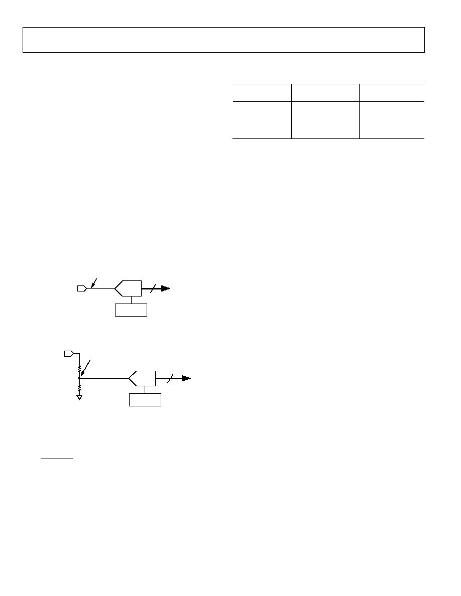
The inputs to the ADC come directly from the VXn pins and
from the back of the input attenuators on the VPn and VH pins,
as shown in Figure 30 and Figure 31.
04609-025
VXn
2.048V VREF
NO ATTENUATION
12-BIT
ADC
DIGITIZED
VOLTAGE
READING
Figure 30. ADC Reading on VXn Pins
04609-026
2.048V VREF
ATTENUATION NETWORK
(DEPENDS ON RANGE SELECTED)
12-BIT
ADC
DIGITIZED
VOLTAGE
READING
VPn/VH
Figure 31. ADC Reading on VPn/VH Pins
The voltage at the input pin can be derived from the following
equation:
V =
4095
Code
ADC
◊ Attenuation Factor ◊ 2.048 V
The ADC input voltage ranges for the SFD input ranges are
listed in Table 8.
Table 8. ADC Input Voltage Ranges
SFD Input
Range (V)
Attenuation Factor
ADC Input Voltage
Range (V)
0.573≠1.375 1
0≠2.048
1.25≠3 2.181
0≠4.46
2.5≠6 4.363
0≠6.0
1
4.8≠14.4 10.472
0≠14.4
1
_______________________________________________
1
The upper limit is the absolute maximum allowed voltage on these pins.
The normal way to supply the reference to the ADC on the
REFIN pin is to simply connect the REFOUT pin to the REFIN
pin. REFOUT provides a 2.048 V reference. As such, the
supervising range covers less than half of the normal ADC
range. It is possible, however, to provide the ADC with a more
accurate external reference for improved readback accuracy.
Supplies can also be connected to the input pins purely for ADC
readback, even though they might go above the expected super-
visory range limits (but not above 6 V, because this violates the
absolute maximum ratings on these pins). For instance, a 1.5 V
supply connected to the VX1 pin can be correctly read out as an
ADC code of approximately 3/4 full scale, but it always sits
above any supervisory limits that can be set on that pin. The
maximum setting for the REFIN pin is 2.048 V.
SUPPLY SUPERVISION WITH THE ADC
In addition to the readback capability, a further level of supervi-
sion is provided by the on-chip 12-bit ADC. The ADM1066 has
limit registers on which the user can program to a maximum or
minimum allowable threshold. Exceeding the threshold generates
a warning that can either be read back from the status registers
or input into the SE to determine what sequencing action the
ADM1066 should take. Only one register is provided for each
input channel, so a UV or OV threshold (but not both) can be
set for a given channel. The round-robin circuit can be enabled
via an SMBus write, or it can be programmed to turn on in any
state in the SE program. For example, it can be set to start once
a power-up sequence is complete and all supplies are known to
be within expected tolerance limits.
Note that a latency is built into this supervision, dictated by the
conversion time of the ADC. With all 12 channels selected, the
total time for the round-robin operation (averaging off) is
approximately 6 ms (500 µs per channel selected). Supervision
using the ADC, therefore, does not provide the same real time
response as the SFDs.

ADM1066
Rev. 0 | Page 21 of 32
SUPPLY MARGINING
OVERVIEW
It is often necessary for the system designer to adjust supplies,
either to optimize their level or force them away from nominal
values to characterize the system performance under these
conditions. This is a function typically performed during an in-
circuit test (ICT), such as when the manufacturer, for example,
wants to guarantee that the product under test functions
correctly at nominal supplies minus 10%.
OPEN-LOOP MARGINING
The simplest method of margining a supply is to implement an
open-loop technique. A popular method for this is to switch
extra resistors into the feedback node of a power module, such
as a dc/dc converter or low dropout regulator (LDO). The extra
resistor alters the voltage at the feedback or trim node and
forces the output voltage to margin up or down by a certain
amount.
The ADM1066 can perform open-loop margining for up to six
supplies. The six on-board voltage DACs (DAC1≠6) can drive
into the feedback pins of the power modules to be margined.
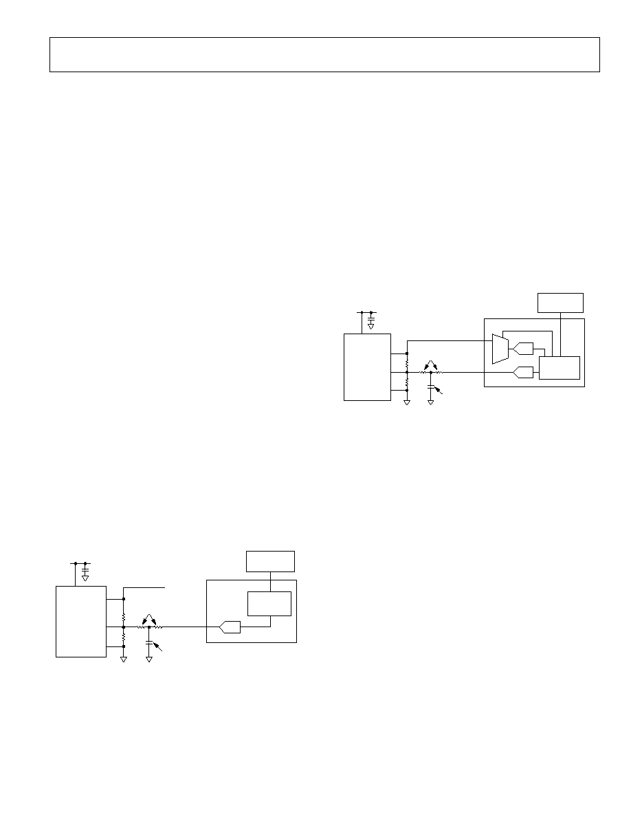
The simplest circuit to implement this function is an attenua-
tion resistor, which connects the DACn pin to the feedback
node of a dc/dc converter. When the DACn output voltage is set
equal to the feedback voltage, no current flows in the attenua-
tion resistor, and the dc/dc output voltage does not change.
Taking DACn above the feedback voltage forces current into the
feedback node, and the output of the dc/dc converter is forced
to fall to compensate for this. The dc/dc output can be forced
high by setting the DACn output voltage lower than the
feedback node voltage. The series resistor can be split in two,
and the node between them decoupled with a capacitor to
ground. This can help to decouple any noise picked up from the
board. Decoupling to a ground local to the dc/dc converter is
recommended.
04609-067
OUTPUT
DC/DC
CONVERTER
FEEDBACK
GND
ATTENUATION
RESISTOR
PCB
TRACE NOISE
DECOUPLING
CAPACITOR
ADM1066
DACOUTn
V
OUT
DAC
µ
CONTROLLER
VIN
DEVICE
CONTROLLER
(SMBus)
Figure 32. Open-Loop Margining System Using the ADM1066
The ADM1066 can be commanded to margin a supply up or
down over the SMBus by updating the values on the relevant
DAC output.
CLOSED-LOOP SUPPLY MARGINING
A much more accurate and comprehensive method of margin-
ing is to implement a closed-loop system. The voltage on the
rail to be margined can be read back so that the rail can be
accurately margined to the target voltage. The ADM1066
incorporates all the circuits required to do this, with the 12-bit
successive approximation ADC used to read back the level of
the supervised voltages, and the six voltage output DACs,
implemented as described in the Open-Loop Margining section,
used to adjust supply levels. These circuits can be used along
with some other intelligence such as a microcontroller to
implement a closed-loop margining system that allows any
dc/dc or LDO supply to be set to any voltage, accurate to within
±0.5% of the target.
04609-
034
OUTPUT
DC/DC
CONVERTER
FEEDBACK
GND
R1
R2
ATTENUATION
RESISTOR, R3
PCB
TRACE NOISE
DECOUPLING
CAPACITOR
VH/VPn/VXn
ADM1066
DACOUTn
MUX
ADC
DAC
DEVICE
CONTROLLER
(SMBus)
µ
CONTROLLER
VIN
Figure 33. Closed-Loop Margining System Using the ADM1066
To implement closed-loop margining:
1. Disable the six DACn outputs.
2. Set the DAC output voltage equal to the voltage on the
feedback node.
3. Enable the DAC.
4. Read the voltage at the dc/dc output, which is connected to
one of the VP1≠4, VH, or VX1≠5 pins.
5. If necessary, modify the DACn output code up or down to
adjust the dc/dc output voltage; otherwise, stop, because
the target voltage has been reached.
6. Set the DAC output voltage to a value that alters the supply
output by the required amount (for example, ±5%).
7. Repeat from Step 4.
Steps 1 to 3 ensure that when the DACn output buffer is turned
on it has little effect on the dc/dc output. The DAC output buffer
is designed to power up without glitching by first powering up
the buffer to follow the pin voltage. It does not drive out onto
the pin at this time. Once the output buffer is properly enabled,
the buffer input is switched over to the DAC, and the output
stage of the buffer is turned on. Output glitching is negligible.

ADM1066
Rev. 0 | Page 22 of 32
WRITING TO THE DACs
Four DAC ranges are offered. They can be placed with midcode
(Code 0x7F) at 0.6 V, 0.8 V, 1.0 V, and 1.25 V. These voltages are
placed to correspond to the most common feedback voltages.
Centering the DAC outputs in this way provides the best use of
the DAC resolution. For most supplies it is possible to place the
DAC midcode at the point where the dc/dc output is not
modified, thereby giving half of the DAC range to margin up
and the other half to margin down.
The DAC output voltage is set by the code written to the DACn
register. The voltage is linear with the unsigned binary number
in this register. Code 0x7F is placed at the midcode voltage, as
described previously. The output voltage is given by the
following equation:
DAC Output = (DACn - 0x7F)/255 ◊ 0.6015 + V
OFF
where V
OFF
is one of the four offset voltages.
There are 256 DAC settings available. The midcode value is
located at DAC code 0x7F as close as possible to the middle
of the 256 code range. The full output swing of the DACs is
+302 mV (+128 codes) and -300 mV (-127 codes) around the
selected midcode voltage. The voltage range for each midcode
voltage is shown in Table 9.
Table 9. Ranges for Midcode Voltages
Midcode
Voltage (V)
Minimum Voltage
Output (V)
Maximum Voltage
Output (V)
0.6 0.300 0.902
0.8 0.500 1.102
1.0 0.700 1.302
1.25 0.950 1.552
CHOOSING THE SIZE OF THE ATTENUATION
RESISTOR
How much this DAC voltage swing affects the output voltage of
the dc/dc converter that is being margined is determined by the
size of the attenuation resistor, R3 (see Figure 33).
Because the voltage at the feedback pin remains constant, the
current flowing from the feedback node to GND via R2 is a
constant. Also, the feedback node itself is high impedance. This
means that the current flowing through R1 is the same as the
current flowing through R3. Therefore, direct relationship exists
between the extra voltage drop across R1 during margining and
the voltage drop across R3.
This relationship is given by the equation
V
OUT
=
R3
R1
(
V
FB
-
V
DACOUT
)
where:
V
OUT
is the change in V
OUT
.
V
FB
is the voltage at the feedback node of the dc/dc converter.
V
DACOUT
is the voltage output of the margining DAC.
This equation demonstrates that, if the user wants the output
voltage to change by ±300 mV, then R1 = R3. If the user wants
the output voltage to change by ±600 mV, then R1 = 2 ◊ R3, and
so on.
It is best to use the full DAC output range to margin a supply.
Choosing the attenuation resistor in this way provides the most
resolution from the DAC. In other words, with one DAC code
change, the smallest effect on the dc/dc output voltage is
induced. If the resistor is sized up to use a code such as 27(dec)
to 227(dec) to move the dc/dc output by ±5%, then it takes
100 codes to move 5% (each code moves the output by 0.05%).
This is beyond the readback accuracy of the ADC, but should
not prevent the user from building a circuit to use the most
resolution.
DAC LIMITING/OTHER SAFETY FEATURES
Limit registers (called DPLIMn and DNLIMn) on the device
offer the user some protection from firmware bugs, which can
cause catastrophic board problems by forcing supplies beyond
their allowable output ranges. Essentially, the DAC code written
into the DACn register is clipped such that the code used to set
the DAC voltage is actually given by
DAC Code
= DACn, DACn DNLIMn and DACn DPLIMn
= DNLIMn,
DACn < DNLIMn
= DPLIMn,
DACn > DPLIMn
In addition, the DAC output buffer is three-stated, if DNLIMn >
DPLIMn. By programming the limit registers in this way, the
user can make it very difficult for the DAC output buffers to be
turned on at all during normal system operation (these are
among the registers downloaded from EEPROM at startup).

ADM1066
Rev. 0 | Page 23 of 32
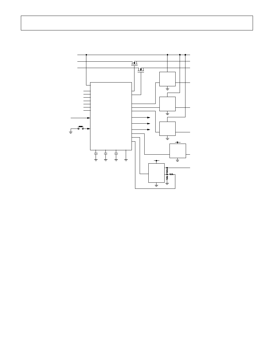
APPLICATIONS DIAGRAM
04608-068
3.3V OUT
3.3V OUT
VH
PDO8
PDO9
PDO10
SYSTEM RESET
PDO7
SIGNAL_VALID
PDO6
POWER_GOOD
PDO2
DAC1*
PDO1
PDO5
PDO4
PDO3
EN
OUT
DC-DC1
IN
3.3V OUT
3V OUT
5V OUT
12V OUT
EN
OUT
DC-DC2
IN
2.5V OUT
EN
OUT
DC-DC3
IN
EN
OUT
LDO
IN
1.8V OUT
0.9V OUT
1.2V OUT
5V OUT
12V IN
5V IN
3V IN
VP1
3V OUT
VP2
3.3V OUT
VP3
2.5V OUT
VP4
1.8V OUT
VX1
1.2V OUT
VX2
0.9V OUT
VX3
POWER_ON
VX4
RESET_L
VX5
10
µ
F
REFIN
10
µ
F
VCCP
10
µ
F
VDDCAP GND
EN
TRIM
OUT
DC-DC4
IN
ADM1066
*ONLY ONE MARGINING CIRCUIT
SHOWN FOR CLARITY. DAC1 TO DAC6
WILL ALLOW MARGINING FOR UP TO
SIX VOLTAGE RAILS.
Figure 34. Applications Diagram

ADM1066
Rev. 0 | Page 24 of 32
COMMUNICATING WITH THE ADM1066
CONFIGURATION DOWNLOAD AT POWER-UP
The configuration of the ADM1066 (UV/OV thresholds, glitch
filter timeouts, PDO configurations, and so on) is dictated by
the contents of RAM. The RAM is comprised of digital latches
that are local to each of the functions on the device. The latches
are double-buffered and have two identical latches, Latch A and
Latch B. Therefore, when an update to a function occurs, the
contents of Latch A are updated first, and then the contents of
Latch B are updated with identical data. The advantages of this
architecture are explained in detail in this section.
The latches are volatile memory and lose their contents at
power-down. Therefore, the configuration in the RAM must be
restored at power-up by downloading the contents of the
EEPROM (nonvolatile memory) to the local latches. This
download occurs in steps, as follows:
1.
With no power applied to the device, the PDOs are all high
impedance.
2.
When 1 V appears on any of the inputs connected to the
VDD arbitrator (VH or VPn), the PDOs are all weakly
pulled to GND with a 20 k impedance.
3.
When the supply rises above the undervoltage lockout of
the device (UVLO is 2.5 V), the EEPROM starts to
download to the RAM.
4.
The EEPROM downloads its contents to all Latch As.
5.
Once the contents of the EEPROM are completely
downloaded to the Latch As, the device controller signals
all Latch As to download to all Latch Bs simultaneously,
completing the configuration download.
6.
At 0.5 ms after the configuration download completes, the
first state definition is downloaded from EEPROM into
the SE.
Note that any attempt to communicate with the device prior to
the completion of the download causes the ADM1066 to issue
a no acknowledge (NACK).
UPDATING THE CONFIGURATION
After power-up, with all the configuration settings loaded from
EEPROM into the RAM registers, the user might need to alter
the configuration of functions on the ADM1066, such as chang-
ing the UV or OV limit of an SFD, changing the fault output of
an SFD, or adjusting the rise time delay of one of the PDOs.
The ADM1066 provides several options that allow the user to
update the configuration over the SMBus interface. The
following options are controlled in the UPDCFG register:
1.
Update the configuration in real time. The user writes to
RAM across the SMBus and the configuration is updated
immediately.
2.
Update the Latch As without updating the Latch Bs. With
this method, the configuration of the ADM1066 remains
unchanged and continues to operate in the original setup
until the instruction is given to update the Latch Bs.
3.
Change EEPROM register contents without changing the
RAM contents, and then download the revised EEPROM
contents to the RAM registers. Again, with this method, the
configuration of the ADM1066 remains unchanged and
continues to operate in the original setup until the
instruction is given to update the RAM.
The instruction to download from the EEPROM in Option 3 is
also a useful way to restore the original EEPROM contents, if
revisions to the configuration are unsatisfactory. For example, if
the user needs to alter an OV threshold, this can be done by
updating the RAM register as described in Option 1. However,
if the user is not satisfied with the change and wants to revert to
the original programmed value, then the device controller can
issue a command to download the EEPROM contents to the
RAM again, as described in Option 3, restoring the ADM1066
to its original configuration.
The topology of the ADM1066 makes this type of operation
possible. The local, volatile registers (RAM) are all double-
buffered latches. Setting Bit 0 of the UPDCFG register to 1
leaves the double-buffered latches open at all times. If Bit 0 is set
to 0, then, when a RAM write occurs across the SMBus, only the
first side of the double-buffered latch is written to. The user
must then write a 1 to Bit 1 of the UPDCFG register. This
generates a pulse to update all the second latches at once.
EEPROM writes occur in a similar way.
The final bit in this register can enable or disable EEPROM
page erasure. If this bit is set high, the contents of an EEPROM
page can all be set to 1. If low, then the contents of a page
cannot be erased, even if the command code for page erasure is
programmed across the SMBus. The bitmap for the UPDCFG
register is shown in the AN-698 application note. A flow chart
for download at power-up and subsequent configuration
updates is shown in Figure 35.

ADM1066
Rev. 0 | Page 25 of 32
04609-035
POWER-UP
(V
CC
> 2.5V)
EEPROM
E
E
P
R
O
M
L
D
D
A
T
A
R
A
M
L
D
U
P
D
SMBus
DEVICE
CONTROLLER
LATCH A
LATCH B
FUNCTION
(OV THRESHOLD
ON VP1)
Figure 35. Configuration Update Flow Diagram
UPDATING THE SEQUENCING ENGINE
Sequencing engine (SE) functions are not updated in the same
way as regular configuration latches. The SE has its own
dedicated 512-byte EEPROM for storing state definitions,
providing 63 individual states with a 64-bit word each (one state
is reserved). At power-up, the first state is loaded from the SE
EEPROM into the engine itself. When the conditions of this
state are met, the next state is loaded from EEPROM into the
engine, and so on. The loading of each new state takes approxi-
mately 10 µs.
To alter a state, the required changes must be made directly to
EEPROM. RAM for each state does not exist. The relevant
alterations must be made to the 64-bit word, which is then
uploaded directly to EEPROM.
INTERNAL REGISTERS
The ADM1066 contains a large number of data registers. The
principal registers are the address pointer register and the
configuration registers.
Address Pointer Register
This register contains the address that selects one of the other
internal registers. When writing to the ADM1066, the first byte
of data is always a register address, which is written to the
address pointer register.
Configuration Registers
These registers provide control and configuration for various
operating parameters of the ADM1066.
EEPROM
The ADM1066 has two 512-byte cells of nonvolatile, electrically
erasable, programmable read-only memory (EEPROM), from
Register Addresses 0xF800 to 0xFBFF. The EEPROM is used for
permanent storage of data that is not lost when the ADM1066 is
powered down. One EEPROM cell contains the configuration
data of the device; the other contains the state definitions for
the SE. Although referred to as read-only memory, the
EEPROM can be written to as well as read from via the serial
bus in exactly the same way as the other registers.
The major differences between the EEPROM and other
registers are
∑
An EEPROM location must be blank before it can be
written to. If it contains data, it must first be erased.
∑
Writing to EEPROM is slower than writing to RAM.
∑
Writing to the EEPROM should be restricted, because it
has a limited write/cycle life of typically 10,000 write
operations due to the usual EEPROM wear-out
mechanisms.
The first EEPROM is split into 16 (0 to 15) pages of 32 bytes
each. Pages 0 to 6, starting at Address 0xF800, hold the
configuration data for the applications on the ADM1066 (the
SFDs, PDOs, and so on). These EEPROM addresses are the
same as the RAM register addresses, prefixed by F8. Page 7 is
reserved. Pages 8 to 15 are for customer use.
Data can be downloaded from EEPROM to RAM in one of the
following ways:
∑
At power-up, when Pages 0 to 6 are downloaded.
∑
By setting Bit 0 of the UDOWNLD register (0xD8), which
performs a user download of Pages 0 to 6.
SERIAL BUS INTERFACE
The ADM1066 is controlled via the serial system management
bus (SMBus). The ADM1066 is connected to this bus as a slave
device, under the control of a master device. It takes approxi-
mately 1 ms after power-up for the ADM1066 to download
from its EEPROM. Therefore, access to the ADM1066 is re-
stricted until the download is completed.
Identifying the ADM1066 on the SMBus
The ADM1060 has a 7-bit serial bus slave address. The device is
powered up with a default serial bus address. The five MSBs of
the address are set to 01101; the two LSBs are determined by the
logical states of Pins A1 and A0. This allows the connection of
four ADM1066s to one SMBus.

ADM1066
Rev. 0 | Page 26 of 32
The device also has several identification registers (read-only),
which can be read across the SMBus. Table 10 lists these registers
with their values and functions.
Table 10. Identification Register Values and Functions
Name
Address
Value
Function
MANID
0xF4
0x41
Manufacturer ID for Analog
Devices
REVID
0xF5
0x00
Silicon revision
MARK1
0xF6
0x00
S/w brand
MARK2
0xF7
0x00
S/w brand
General SMBus Timing
Figure 36, Figure 37, and Figure 38 are timing diagrams for
general read and write operations using the SMBus. The SMBus
specification defines specific conditions for different types of
read and write operations, which are discussed in the Write
Operations and Read Operations sections.
The general SMBus protocol operates as follows:
1.
The master initiates data transfer by establishing a start
condition, defined as a high-to-low transition on the serial
data-line SDA, while the serial clock-line SCL remains
high. This indicates that a data stream follows. All slave
peripherals connected to the serial bus respond to the start
condition and shift in the next 8 bits, consisting of a 7-bit
slave address (MSB first) plus a R/W bit. This bit deter-
mines the direction of the data transfer, that is, whether
data is written to or read from the slave device (0 = write,
1 = read).
The peripheral whose address corresponds to the transmit-
ted address responds by pulling the data line low during
the low period before the ninth clock pulse, known as the
acknowledge bit, and holding it low during the high period
of this clock pulse.
All other devices on the bus remain idle while the selected
device waits for data to be read from or written to it. If the
R/W bit is a 0, the master writes to the slave device. If the
R/W bit is a 1, the master reads from the slave device.
2.
Data is sent over the serial bus in sequences of nine clock
pulses, eight bits of data followed by an acknowledge bit
from the slave device. Data transitions on the data line
must occur during the low period of the clock signal and
remain stable during the high period, because a low-to-
high transition when the clock is high might be interpreted
as a stop signal. If the operation is a write operation, the
first data byte after the slave address is a command byte.
This tells the slave device what to expect next. It might be
an instruction telling the slave device to expect a block
write, or it might simply be a register address that tells the
slave where subsequent data is to be written. Because data
can flow in only one direction, as defined by the R/W bit,
sending a command to a slave device during a read
operation is not possible. Before a read operation, it might
be necessary to perform a write operation to tell the slave
what sort of read operation to expect and/or the address
from which data is to be read.
3.
When all data bytes have been read or written, stop condi-
tions are established. In write mode, the master pulls the
data line high during the 10th clock pulse to assert a stop
condition. In read mode, the master device releases the
SDA line during the low period before the ninth clock
pulse, but the slave device does not pull it low. This is
known as no acknowledge. The master then takes the data
line low during the low period before the tenth clock pulse,
then high during the tenth clock pulse to assert a stop
condition.
04609-036
1
9
9
1
1
9
1
9
START BY
MASTER
ACK. BY
SLAVE
ACK. BY
SLAVE
ACK. BY
SLAVE
ACK. BY
SLAVE
FRAME 2
COMMAND CODE
FRAME 1
SLAVE ADDRESS
FRAME N
DATA BYTE
FRAME 3
DATA BYTE
SCL
SDA
R/W
STOP
BY
MASTER
SCL
(CONTINUED)
SDA
(CONTINUED)
D7
A0
A1
1
1
1
0
0
D6
D5
D4
D3
D2
D1
D0
D7
D6
D5
D4
D3
D2
D1
D0
D7
D6
D5
D4
D3
D2
D1
D0
Figure 36. General SMBus Write Timing Diagram

ADM1066
Rev. 0 | Page 27 of 32
9
04609-037
1
9
9
1
1
9
1
START BY
MASTER
ACK. BY
SLAVE
ACK. BY
MASTER
ACK. BY
MASTER
NO ACK.
FRAME 2
DATA BYTE
FRAME 1
SLAVE ADDRESS
FRAME N
DATA BYTE
FRAME 3
DATA BYTE
SCL
SDA
R/W
STOP
BY
MASTER
SCL
(CONTINUED)
SDA
(CONTINUED)
D7
A0
A1
1
1
1
0
0
D6
D5
D4
D3
D2
D1
D0
D7
D6
D5
D4
D3
D2
D1
D0
D7
D6
D5
D4
D3
D2
D1
D0
Figure 37. General SMBus Read Timing Diagram
04609-038
SCL
SDA
P
S
S
P
t
SU; STO
t
HD;STA
t
SU;STA
t
SU; DAT
t
HD;DAT
t
HD; STA
t
HI G H
t
BUF
t
LO W
t
R
t
F
Figure 38. Serial Bus Timing Diagram
SMBus Protocols for RAM and EEPROM
The ADM1066 contains volatile registers (RAM) and nonvola-
tile registers (EEPROM). User RAM occupies address locations
from 0x00 to 0xDF; EEPROM occupies addresses from 0xF800
to 0xFBFF.
Data can be written to and read from both RAM and EEPROM
as single data bytes. Data can be written only to unprogrammed
EEPROM locations. To write new data to a programmed loca-
tion, it must first be erased. EEPROM erasure cannot be done at
the byte level. The EEPROM is arranged as 32 pages of 32 bytes
each, and an entire page must be erased.
Page erasure is enabled by setting Bit 2 in the UPDCFG register
(Address 0x90) to 1. If this bit is not set, page erasure cannot
occur, even if the command byte (0xFE) is programmed across
the SMBus.
WRITE OPERATIONS
The SMBus specification defines several protocols for different
types of read and write operations. The following abbreviations
are used in the diagrams:
S Start
P Stop
R Read
W Write
A Acknowledge
A
No acknowledge
The ADM1066 uses the following SMBus write protocols.
Send Byte
In a send byte operation, the master device sends a single
command byte to a slave device, as follows:
1.
The master device asserts a start condition on SDA.
2.
The master sends the 7-bit slave address followed by the
write bit (low).
3.
The addressed slave device asserts ACK on SDA.
4.
The master sends a command code.
5.
The slave asserts ACK on SDA.
6.
The master asserts a stop condition on SDA and the
transaction ends.
In the ADM1066, the send byte protocol is used for two
purposes:
∑
To write a register address to RAM for a subsequent single
byte read from the same address, or a block read or write
starting at that address, as shown in Figure 39.
04609-039
2
4
1
3
SLAVE
ADDRESS
REGISTER
ADDRESS
(0x00 TO 0xDF)
S
W A
A
5
6
P
Figure 39. Setting a RAM Address for Subsequent Read

ADM1066
Rev. 0 | Page 28 of 32
5
6
P
∑
To erase a page of EEPROM memory. EEPROM memory
can be written to only if it is unprogrammed. Before
writing to one or more EEPROM memory locations that
are already programmed, the page or pages containing
those locations must first be erased. EEPROM memory is
erased by writing a command byte.
The master sends a command code that tells the slave
device to erase the page. The ADM1066 command code for
a page erasure is 0xFE (1111 1110). Note that, for a page
erasure to take place, the page address has to be given in
the previous write word transaction (see the Write
Byte/Word section). Also, Bit 2 in the UPDCFG register
(Address 0x90) must be set to 1.
04609-040
2
4
1
3
SLAVE
ADDRESS
COMMAND
BYTE
(0xFE)
S
W
A
A
Figure 40. EEPROM Page Erasure
As soon as the ADM1066 receives the command byte, page
erasure begins. The master device can send a stop
command as soon as it sends the command byte. Page
erasure takes approximately 20 ms. If the ADM1066 is
accessed before erasure is complete, it responds with a no
acknowledge (NACK).
Write Byte/Word
In a write byte/word operation, the master device sends a
command byte and one or two data bytes to the slave device, as
follows:
1.
The master device asserts a start condition on SDA.
2.
The master sends the 7-bit slave address followed by the
write bit (low).
3.
The addressed slave device asserts ACK on SDA.
4.
The master sends a command code.
5.
The slave asserts ACK on SDA.
6.
The master sends a data byte.
7.
The slave asserts ACK on SDA.
8.
The master sends a data byte (or asserts a stop condition at
this point).
9.
The slave asserts ACK on SDA.
10.
The master asserts a stop condition on SDA to end the
transaction.
In the ADM1066, the write byte/word protocol is used for three
purposes:
∑
To write a single byte of data to RAM. In this case, the
command byte is the RAM address from 0x00 to 0xDF and
the only data byte is the actual data, as shown in Figure 41.
04609-041
SLAVE
ADDRESS
RAM
ADDRESS
(0x00 TO 0xDF)
S
W A
DATA
A
P
A
2
4
1
3
5
7
6
8
Figure 41. Single Byte Write to RAM
∑
To set up a 2-byte EEPROM address for a subsequent read,
write, block read, block write, or page erase. In this case, the
command byte is the high byte of the EEPROM address
from 0xF8 to 0xFB. The only data byte is the low byte of
the EEPROM address, as shown in Figure 42.
04609-042
SLAVE
ADDRESS
EEPROM
ADDRESS
HIGH BYTE
(0xF8 TO 0xFB)
S
W A
EEPROM
ADDRESS
LOW BYTE
(0x00 TO 0xFF)
A
P
A
2
4
1
3
5
7
6
8
Figure 42. Setting an EEPROM Address
Note, for page erasure, that because a page consists of
32 bytes, only the three MSBs of the address low byte are
important. The lower five bits of the EEPROM address low
byte specify the addresses within a page and are ignored
during an erase operation.
∑
To write a single byte of data to EEPROM. In this case, the
command byte is the high byte of the EEPROM address
from 0xF8 to 0xFB. The first data byte is the low byte of the
EEPROM address, and the second data byte is the actual
data, as shown in Figure 43.
04609-043
SLAVE
ADDRESS
EEPROM
ADDRESS
HIGH BYTE
(0xF8 TO 0xFB)
S
W A
EEPROM
ADDRESS
LOW BYTE
(0x00 TO 0xFF)
A
P
A
2
4
1
3
5
7
A
9
DATA
8
6
10
Figure 43. Single Byte Write to EEPROM
Block Write
In a block write operation, the master device writes a block of
data to a slave device. The start address for a block write must
have been set previously. In the ADM1066, a send byte opera-
tion sets a RAM address, and a write byte/word operation sets
an EEPROM address, as follows:
1.
The master device asserts a start condition on SDA.
2.
The master sends the 7-bit slave address followed by
the write bit (low).
3.
The addressed slave device asserts ACK on SDA.
4.
The master sends a command code that tells the slave
device to expect a block write. The ADM1066 command
code for a block write is 0xFC (1111 1100).

ADM1066
Rev. 0 | Page 29 of 32
5.
The slave asserts ACK on SDA.
6.
The master sends a data byte that tells the slave device how
many data bytes are being sent. The SMBus specification
allows a maximum of 32 data bytes in a block write.
7.
The slave asserts ACK on SDA.
8.
The master sends N data bytes.
9.
The slave asserts ACK on SDA after each data byte.
10.
The master asserts a stop condition on SDA to end the
transaction.
04609-
044
SLAVE
ADDRESS
S
W A
2
COMMAND 0xFC
(BLOCK WRITE)
4
1
3
A
5
BYTE
COUNT
6
A
7
A
9
10
A P
A
DATA
1
8
DATA
N
DATA
2
Figure 44. Block Write to EEPROM or RAM
Unlike some EEPROM devices that limit block writes to within
a page boundary, there is no limitation on the start address
when performing a block write to EEPROM, except
∑
There must be at least N locations from the start address to
the highest EEPROM address (0xFBFF), to avoid writing to
invalid addresses.
∑
If the addresses cross a page boundary, both pages must be
erased before programming.
Note that the ADM1066 features a clock extend function for
writes to EEPROM. Programming an EEPROM byte takes
approximately 250 µs, which would limit the SMBus clock for
repeated or block write operations. The ADM1066 pulls SCL
low and extends the clock pulse when it cannot accept any
more data.
READ OPERATIONS
The ADM1066 uses the following SMBus read protocols.
Receive Byte
In a receive byte operation, the master device receives a single
byte from a slave device, as follows:
1.
The master device asserts a start condition on SDA.
2.
The master sends the 7-bit slave address followed by the
read bit (high).
3.
The addressed slave device asserts ACK on SDA.
4.
The master receives a data byte.
5.
The master asserts no acknowledge on SDA.
6.
The master asserts a stop condition on SDA, and the
transaction ends.
In the ADM1066, the receive byte protocol is used to read a
single byte of data from a RAM or EEPROM location whose
address has previously been set by a send byte or write
byte/word operation, as shown in Figure 45.
04609-045
2
3
1
4
5
SLAVE
ADDRESS
S
R
DATA
P
A
6
A
Figure 45. Single Byte Read from EEPROM or RAM
Block Read
In a block read operation, the master device reads a block of
data from a slave device. The start address for a block read must
have been set previously. In the ADM1066, this is done by a
send byte operation to set a RAM address, or a write byte/word
operation to set an EEPROM address. The block read operation
itself consists of a send byte operation that sends a block read
command to the slave, immediately followed by a repeated start
and a read operation that reads out multiple data bytes, as
follows:
1.
The master device asserts a start condition on SDA.
2.
The master sends the 7-bit slave address followed by the
write bit (low).
3.
The addressed slave device asserts ACK on SDA.
4.
The master sends a command code that tells the slave
device to expect a block read. The ADM1066 command
code for a block read is 0xFD (1111 1101).
5.
The slave asserts ACK on SDA.
6.
The master asserts a repeat start condition on SDA.
7.
The master sends the 7-bit slave address followed by the
read bit (high).
8.
The slave asserts ACK on SDA.
9.
The ADM1066 sends a byte-count data byte that tells the
master how many data bytes to expect. The ADM1066
always returns 32 data bytes (0x20), which is the maximum
allowed by the SMBus 1.1 specification.
10.
The master asserts ACK on SDA.
11.
The master receives 32 data bytes.
12.
The master asserts ACK on SDA after each data byte.
13.
The master asserts a stop condition on SDA to end the
transaction.

ADM1066
Rev. 0 | Page 30 of 32
04609-046
SLAVE
ADDRESS
S
W A
2
COMMAND 0xFD
(BLOCK READ)
4
1
3
A
5
S
6
SLAVE
ADDRESS
7
BYTE
COUNT
9
10
12
11
A
R A
8
DATA
1
DATA
32
13
A
14
P
A
Figure 46. Block Read from EEPROM or RAM
Error Correction
The ADM1066 provides the option of issuing a PEC (packet
error correction) byte after a write to RAM, a write to EEPROM,
a block write to RAM/EEPROM, or a block read from RAM/
EEPROM. This enables the user to verify that the data received
by or sent from the ADM1066 is correct. The PEC byte is an
optional byte sent after that last data byte has been written to or
read from the ADM1066. The protocol is as follows:
1.
The ADM1066 issues a PEC byte to the master. The master
checks the PEC byte and issues another block read, if the
PEC byte is incorrect.
2.
A no acknowledge (NACK) is generated after the PEC byte
to signal the end of the read.
Note that the PEC byte is calculated using CRC-8. The frame
check sequence (FCS) conforms to CRC-8 by the polynomial
C(x) = x
8
+
x
2
+
x
1
+ 1
See the SMBus 1.1 specification for details.
An example of a block read with the optional PEC byte is
shown in Figure 47.
04609-047
SLAVE
ADDRESS
S
W A
2
COMMAND 0xFD
(BLOCK READ)
4
1
3
A
5
S
6
SLAVE
ADDRESS
7
BYTE
COUNT
9
10
12
11
A
R A
8
DATA
1
DATA
32
A
13
PEC
14
A
15
P
A
Figure 47. Block Read from EEPROM or RAM with PEC

ADM1066
Rev. 0 | Page 31 of 32
OUTLINE DIMENSIONS
1
40
10
11
31
30
21
20
4.25
4.10 SQ
3.95
TOP
VIEW
6.00
BSC SQ
PIN 1
INDICATOR
5.75
BCS SQ
12∞ MAX
0.30
0.23
0.18
0.20 REF
SEATING
PLANE
1.00
0.85
0.80
0.05 MAX
0.02 NOM
COPLANARITY
0.08
0.80 MAX
0.65 TYP
4.50
REF
0.50
0.40
0.30
0.50
BSC
PIN 1
INDICATOR
0.60 MAX
0.60 MAX
0.25 MIN
EXPOSED
PAD
(BOTTOM VIEW)
COMPLIANT TO JEDEC STANDARDS MO-220-VJJD-2
Figure 48. 40-Lead Lead Frame Chip Scale Package [LFCSP]
(CP-40)
Dimensions shown in millimeters
0.50
BSC
0.27
0.22
0.17
9.00
BSC SQ
1.05
1.00
0.95
7.00
BSC SQ
1.20
MAX
0.20
0.09
TOP VIEW
(PINS DOWN)
1
12
13
25
24
36
37
48
SEATING
PLANE
0.75
0.60
0.45
PIN 1
VIEW A
0.08 MAX
COPLANARITY
VIEW A
ROTATED 90∞ CCW
SEATING
PLANE
0∞ MIN
7∞
3.5∞
0∞
0.15
0.05
COMPLIANT TO JEDEC STANDARDS MS-026ABC
Figure 49. 48-Lead Thin Plastic Quad Flat Package [TQFP]
(SU-48)
Dimensions shown in millimeters
ORDERING GUIDE
Model
Temperature Range
Description
Package Option
ADM1066ACP
-40∞C to +85∞C
40-Lead LFCSP
CP-40
ADM1066ACP-REEL
-40∞C to +85∞C
40-Lead LFCSP
CP-40
ADM1066ACP-REEL7
-40∞C to +85∞C
40-Lead LFCSP
CP-40
ADM1066ASU
-40∞C to +85∞C
48-Lead TQFP
SU-48
ADM1066ASU-REEL
-40∞C to +85∞C
48-Lead TQFP
SU-48
ADM1066ASU-REEL7
-40∞C to +85∞C
48-Lead TQFP
SU-48
EVAL-ADM1066LFEB
ADM1066 Evaluation Kit (LFSCP Version)
EVAL-ADM1066TQEB
ADM1066
Evaluation Kit (TQFP Version)

ADM1066
Rev. 0 | Page 32 of 32
NOTES
© 2004 Analog Devices, Inc. All rights reserved. Trademarks and
registered trademarks are the property of their respective owners.
D04609≠0≠10/04(0)
