Document Outline
- FEATURES
- APPLICATIONS
- GENERAL DESCRIPTION
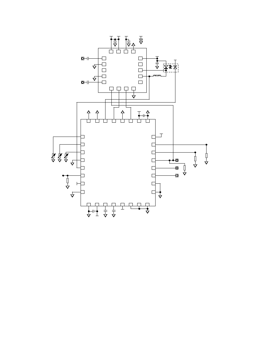
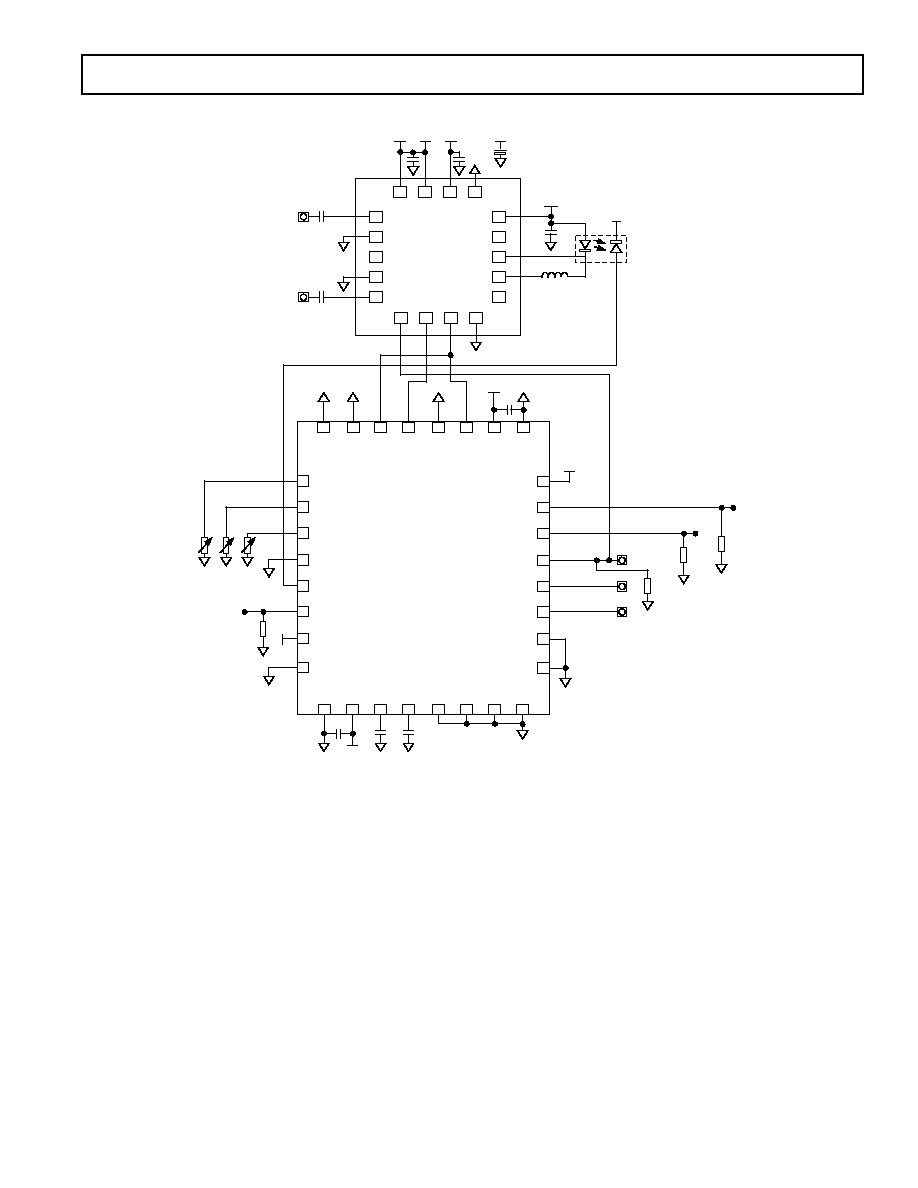
- FUNCTIONAL BLOCK DIAGRAM
- SPECIFICATIONS
- ABSOLUTE MAXIMUM RATINGS
- ORDERING GUIDE
- ADN2844 METALLIZATION PHOTOGRAPH
- ADN2845 METALLIZATION PHOTOGRAPH
- PIN CONFIGURATIONS
- ADN2844 PIN FUNCTION DESCRIPTIONS
- ADN2845 PIN FUNCTION DESCRIPTIONS
- GENERAL
- CONTROL
- PAVCAP AND ERCAP
- ALARMS
- ALARM INTERFACE
- DATA INPUTS
- MONITOR CURRENTS
- MPD CURRENT
- DUAL MPD DWDM FUNCTION
- IDTONE
- AUTOMATIC LASER SHUTDOWN (ALS)
- POWER DISSIPATION
- DIE PAD COORDINATES
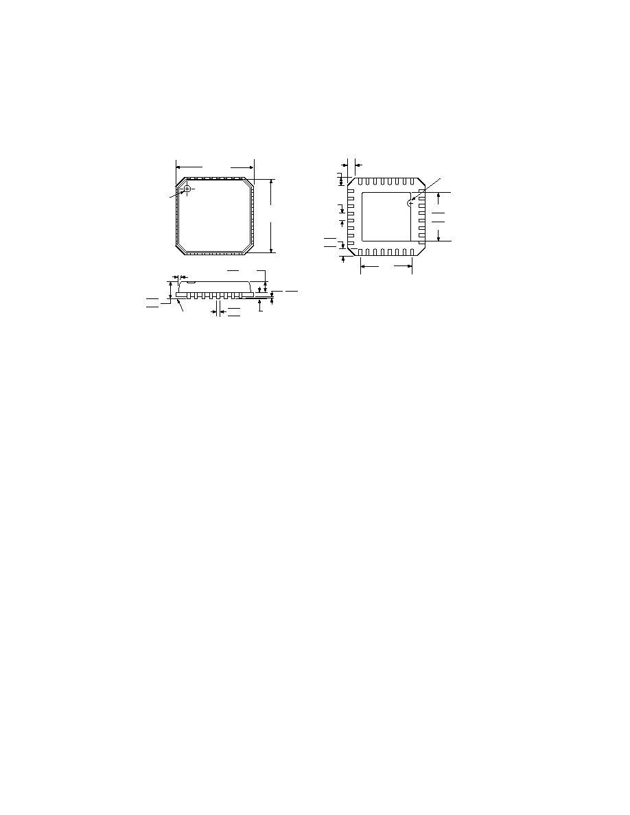
- OUTLINE DIMENSIONS
ADN2843
10.709 Gbps Laser Diode
Driver Chipset
REV. 0
Information furnished by Analog Devices is believed to be accurate and
reliable. However, no responsibility is assumed by Analog Devices for its
use, nor for any infringements of patents or other rights of third parties that
may result from its use. No license is granted by implication or otherwise
under any patent or patent rights of Analog Devices. Trademarks and
registered trademarks are the property of their respective companies.
One Technology Way, P.O. Box 9106, Norwood, MA 02062-9106, U.S.A.
Tel: 781/329-4700
www.analog.com
Fax: 781/326-8703
© 2003 Analog Devices, Inc. All rights reserved.
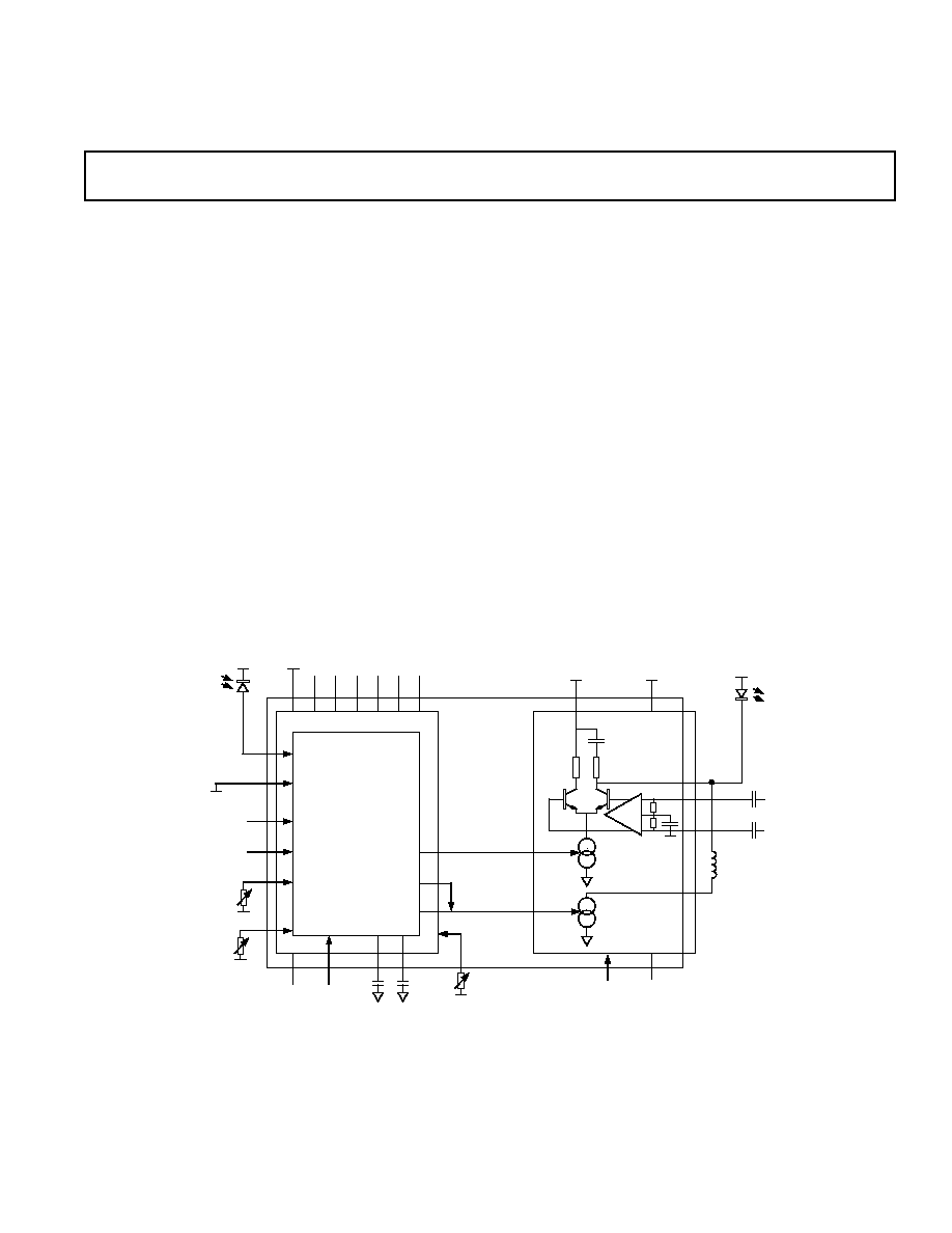
FUNCTIONAL BLOCK DIAGRAM
MPD
V
CC
IMPD
IMPD2
GND
MODE
ALS
ERSET
PSET
IDTONE
ADN2844
IMPDMON
IMPDMON2
IMMON
IBMON
FAIL
DEGRADE
GND
GND
GND
ERCAP
PAVCAP
GND
CONTROL
IBIAS_CTRL
D_IMOD
IMOD_CTRL
V
CC
V
CC
DATAP
DATAN
V
CC
V
CC
ADN2843
ADN2845
IMODN
GND
IBIAS
ALS
*ADN2850 OR ADN2860 OPTICAL SUPERVISOR
LD
GND
IMODP
ASET
*
*
FEATURES
Data Rates from 9.952 Gbps to 10.709 Gbps
Typical Rise/Fall Time 25 ps/23 ps
Bias Current Range 3 mA to 80 mA
Modulation Current Range 5 mA to 80 mA
Monitor Photodiode Current 50 A to 1200 A
Closed-Loop Control of Both Average Optical Power
and Extinction Ratio
Laser Fail and Laser Degrade Alarms
Automatic Laser Shutdown, ALS
Dual MPD Functionality for Wavelength Control
CML Data Inputs
50 Internal Data Terminations
3.3 V Single-Supply Operation
Driver Supplied in Dice Format
APPLICATIONS
SONET OC-192, SDH STM-64
Supports 10.667 Gbps and 10.709 Gbps FEC Rates
10 Gb Ethernet IEEE802.3ae
GENERAL DESCRIPTION
The ADN2943 chipset consists of two components, the ADN2845
and the ADN2844. The ADN2845 is a 10.709 Gbps laser diode
driver. The ADN2845 eliminates the need to ac couple since it
can deliver 80 mA of modulation while dc coupled to the laser
diode. It is intended to be copackaged with the laser to minimize
bond lengths, which improves performance of the optical
transmitter. For transmission line applications, contact HSN
Application Group at fiberoptic.ic@analog.com.
The ADN2844 offers a unique control loop algorithm and pro-
vides dual loop control of both average power and extinction ratio.
Programmable alarms are provided for laser fail (end of life) and
laser degrade (impending fail).
Both the ADN2844 and the ADN2845 are available as bare die.
The ADN2844 is also available in 5 mm
• 5 mm 32-lead LFCSP.
a

REV. 0
≠2≠
ADN2843≠SPECIFICATIONS
(V
CC
= 3.0 V to 3.6 V, All specifications T
MIN
to T
MAX
, unless otherwise noted. Typical
values as specified at 25 C.)
Parameter
Min
Typ
Max
Unit
Conditions
LASER BIAS (BIAS)
Output Current I
BIAS
3
80
mA
Compliance Voltage
1.2
V
CC
≠ 1.0
V
I
BIAS
during ALS
10
A
See Note 1
ALS Shutdown Response Time
10
s
MODULATION CURRENT (IMODP, IMODN)
See Note 2
Output Current I
MOD
5
80
mA
Compliance Voltage
1.2
V
CC
V
I
MOD
during ALS
10
A
Rise Time
25
ps
Fall Time
23
ps
Random Jitter
170
fs rms
See Note 3
Total Jitter
7.41
ps p-p
See Note 4
POWER SET INPUT (PSET)
External Capacitance
80
pF
See Note 5
Voltage
1.15
1.35
V
EXTINCTION RATIO SET INPUT (ERSET)
Allowable Resistance Range
1.5
25
k
Voltage
1.15
1.35
V
ALARM SET (ASET)
Allowable Resistance Range
1.2
13.2
k
Voltage
1.15
1.35
V
Hysteresis
5
%
CONTROL LOOP
Time Constant
0.22
s
DATA INPUTS (DATAP, DATAN)
V p-p (Single-Ended Peak-to-Peak)
300
800
mV
Input Impedance
(Single-Ended)
50
LOGIC INPUTS (ALS, MODE)
V
IH
2.4
V
V
IL
0.8
V
ALARM OUTPUTS (Internal 30 k to V
CC
)
V
OH
2.4
V
V
OL
0.4
V
IDTONE
f
IN
10
1000
kHz
Input Current Range
50
4000
A
Voltage on IDTONE
V
CC
≠ 2
V
MONITOR PD (MPD, MPD2)
Current
50
1200
A
Input Voltage
1.65
V
IBMON, IMMON, IMPDMON, IMPDMON2
IBMON, IMMON Division Ratio
100
A/A
IMPDMON, IMPDMON2
1
A/A
IMPDMON to IMPDMON2 Matching
2
%
Measured at 1200 A
Compliance Voltage
0
V
CC
≠ 1.5
V
SUPPLY
V
CC
3.0
3.3
3.6
V
I
CC
(ADN2844)
36
mA
See Note 6
I
CC
(ADN2845)
75
mA
See Note 6
NOTES
1
In ALS mode current is sourced to the laser from the I
BIAS
pin, which reverse biases the laser.
2
The ADN2845 high speed specifications are measured into a 5 load.
3
RMS jitter measured with a 0000 0000 1111 1111 repeating pattern at 10.7 Gbps rate.
4
Peak-to-peak total jitter measured with a 2
13
≠ 1 PRBS with 80 CIDs pattern at 10.7 Gbps rate.
5
Max capacitance refers to capacitance of photodiode and other parasitic capacitance.
6
I
BIAS
= 0, I
MOD
= 0 (when ALS is asserted). See Power Dissipation section on page 7 for calculation of complete power dissipation.
Specifications subject to change without notice.
REV. 0
ADN2843
≠3≠
ABSOLUTE MAXIMUM RATINGS
*
(T
A
= 25∞C, unless otherwise noted.)
V
CC
to GND . . . . . . . . . . . . . . . . . . . . . . . . . . . . . . . . . . 4.2 V
Digital Inputs (ALS, MODE) . . . . . . . . ≠0.5 V to V
CC
+ 0.3 V
IMODN, IMODP . . . . . . . . . . . . . . . . . . . . . . . . . V
CC
+ 1.2 V
MOD_CONTROL to GND . . . . . . . . . . . . . . ≠0.5 V to 4.2 V
IBIAS_CONTROL to GND . . . . . . . . . . . . . . ≠0.5 V to 4.2 V
D_MOD to GND . . . . . . . . . . . . . . . . . . . . . . ≠0.5 V to 4.2 V
DATAP to GND . . . . . . . . . . . . . . . . . . . . . . . ≠0.5 V to 4.2 V
DATAN to GND . . . . . . . . . . . . . . . . . . . . . . ≠0.5 V to 4.2 V
Operating Temperature Range
Industrial . . . . . . . . . . . . . . . . . . . . . . . . . . . ≠40∞C to +85∞C
Storage Temperature Range . . . . . . . . . . . . . ≠65∞C to +150∞C
Junction Temperature (T
J
Max) . . . . . . . . . . . . . . . . . . 150∞C
*Stresses above those listed under Absolute Maximum Ratings may cause perma-
nent damage to the device. This is a stress rating only; functional operation of the
device at these or any other conditions above those listed in the operational
sections of this specification is not implied. Exposure to absolute maximum rating
conditions for extended periods may affect device reliability.
CAUTION
ESD (electrostatic discharge) sensitive device. Electrostatic charges as high as 4000 V readily
accumulate on the human body and test equipment and can discharge without detection. Although the
ADN2843 features proprietary ESD protection circuitry, permanent damage may occur on devices
subjected to high energy electrostatic discharges. Therefore, proper ESD precautions are recommended
to avoid performance degradation or loss of functionality.
ORDERING GUIDE
Temperature
Package
Model
Range
Option
ADN2843CHIPSET
≠40∞C to +85∞C ADN2844 Control
Loop: 32-Lead LFCSP
ADN2845 Data
Switch: Dice
ADN2843CHIPSET-B ≠40∞C to +85∞C ADN2844 Control
Loop: Dice
ADN2845 Data
Switch: Dice
EVAL-ADN2843
Evaluation Board
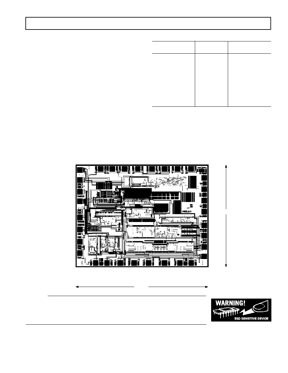
ADN2844 METALLIZATION PHOTOGRAPH
GND
V
CC
MODE
2390 m
3000 m
ERCAP
PAVCAP
GND
GND
GND
GND
GND
DEGRADE
F
AIL
ALS
IMMON
IBMON
IDT
ONE
GND
PSET
ERSET
ASET
IMPD
IMPDMON
IMPDMON2
IMPD2
GND
GND
GND
GND
V
CC
IBIAS_CTRL
IMOD_CTRL
D_IMOD
REV. 0
≠4≠
ADN2843
PIN CONFIGURATIONS
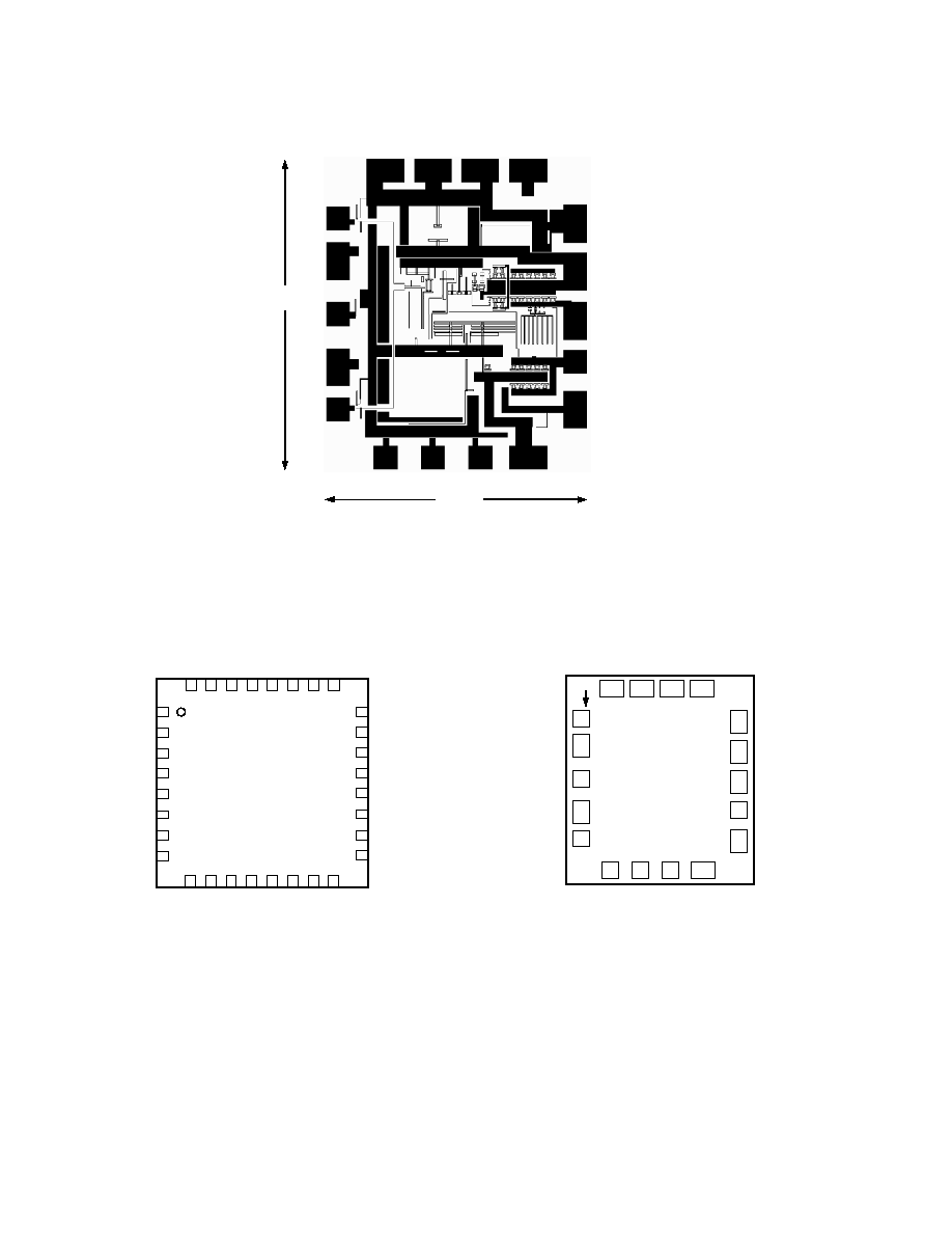
ADN2845 METALLIZATION PHOTOGRAPH
GND
V
CC
V
CC
V
CC
NC
NC
IMODP
IBIAS
GND
IBIAS_CTRL
ALS IMOD_CTRL
GND
DATAP
GND
DATAN
1340 m
( 20 m)
1140 m
( 20 m)
NC
V
CC
(IMODN TERM)
IMPD
ASET
GND
PSET
IMPD2
ERSET
MODE
PAVCAP
GND
GND
GND
ERCAP
GND
V
CC
D_IMOD
V
CC
IBIAS_CTRL
GND
GND
GND
IMOD_CTRL
GND
FAIL
IDTONE
ALS
IMMON
DEGRADE
GND
GND
IBMON
IMPDMON
IMPDMON2
1
2
3
4
5
6
7
8
24
23
22
21
20
19
18
17
32
31
30
29
28
27
26
25
9
10
11
12
13
14
15
16
ADN2844
BOND PAD SIZE: >115 m
BOND PAD PITCH: >104 m
DIE SIZE: 3000 m
2390 m
DATAN
GND
NC
DATAP
GND
V
CC
(IMODN TERM)
NC
IMODP
NC
IBIAS
V
CC
GND
ALS
IMOD_CTRL
IBIAS_CTRL
GND
1
ADN2845
PAD PITCH: 200 m
MAXIMUM DIE SIZE: 1.16mm
1.36mm
DIE THICKNESS: 0.25mm
SINGLE PAD SIZE: 92 m 92 m
DOUBLE PAD SIZE: 151 m 92 m
V
CC
V
CC

REV. 0
ADN2843
≠5≠
ADN2844 PIN FUNCTION DESCRIPTIONS
Pin No.
Mnemonic
Function
1
ASET
Alarm Current Threshold Set (Should be Terminated with a 1.2 k Resistor when Not Used)
2
ERSET
Extinction Ratio Current Set
3
PSET
Average Optical Power Set
4
GND
Negative Supply
5
IMPD
Monitor Photodiode Current Input (Tie to GND when Not in Use)
6
IMPDMON
Mirrored Current from IMPD (Tie to V
CC
when Not in Use)
7
IMPDMON2
Mirrored Current from IMPD2 (For Optional Use with Two MPDs, Tie to V
CC
when Not in Use)
8
IMPD2
Optional Second MPD Current Input (Tie to GND when Not in Use)
9
GND
Negative Supply
10
V
CC
Positive Supply
11
ERCAP
Extinction Ratio Loop Capacitor
12
PAVCAP
Average Power Loop Capacitor
13
MODE
Control Loop Operating Mode Logic Input (Should Not Be Left Floating)
14, 15, 17 GND
Negative Supply
18, 31, 32 GND
Negative Supply
16
GND
Negative Supply
19
DEGRADE
DEGRADE Alarm Output, Open Collector, Active High
20
FAIL
FAIL Alarm Output, Open Collector, Active High
21
ALS
Automatic Laser Shutdown Logic Input (Should Not Be Left Floating)
22
IMMON
Modulation Current Mirror Output, Current Source from V
CC
23
IBMON
Bias Current Mirror Output, Current Source from V
CC
24
IDTONE
ID Tone Input Current (Tie to V
CC
when Not in Use)
25
GND
Negative Supply
26
V
CC
Positive Supply
27
IBIAS_CTRL
Control Output Current Sink
28
GND
Negative Supply
29
IMOD_CTRL Control Output Current Sink
30
D_IMOD
Control Output Current Sink
ADN2845 PIN FUNCTION DESCRIPTIONS
Pin No.
Mnemonic
Function
1
DATAN
AC-Coupled CML Data, Negative Differential Terminal
2
GND
Negative Supply
3, 13
NC
No Connect, Leave Floating
4
GND
Negative Supply
5
DATAP
AC-Coupled CML Data, Positive Differential Terminal
6
ALS
Automatic Laser Shutdown Logic Input
7
IMOD_CTRL
Modulation Current Control Input (Control Circuit Sinks IMOD/10 from Pin to GND)
8
IBIAS_CTRL
BIAS Current Control Input (Control Circuit Sinks IBIAS/10 from Pin to GND)
9
GND
Negative Supply
10
NC
No Connect, Leave Floating
11
IBIAS
BIAS Current
12
IMODP
Modulation Current
14
V
CC
V
CC
Connection for IMODN Termination Resistor
15
GND
Negative Supply
16≠18
V
CC
Positive Supply
REV. 0
≠6≠
ADN2843
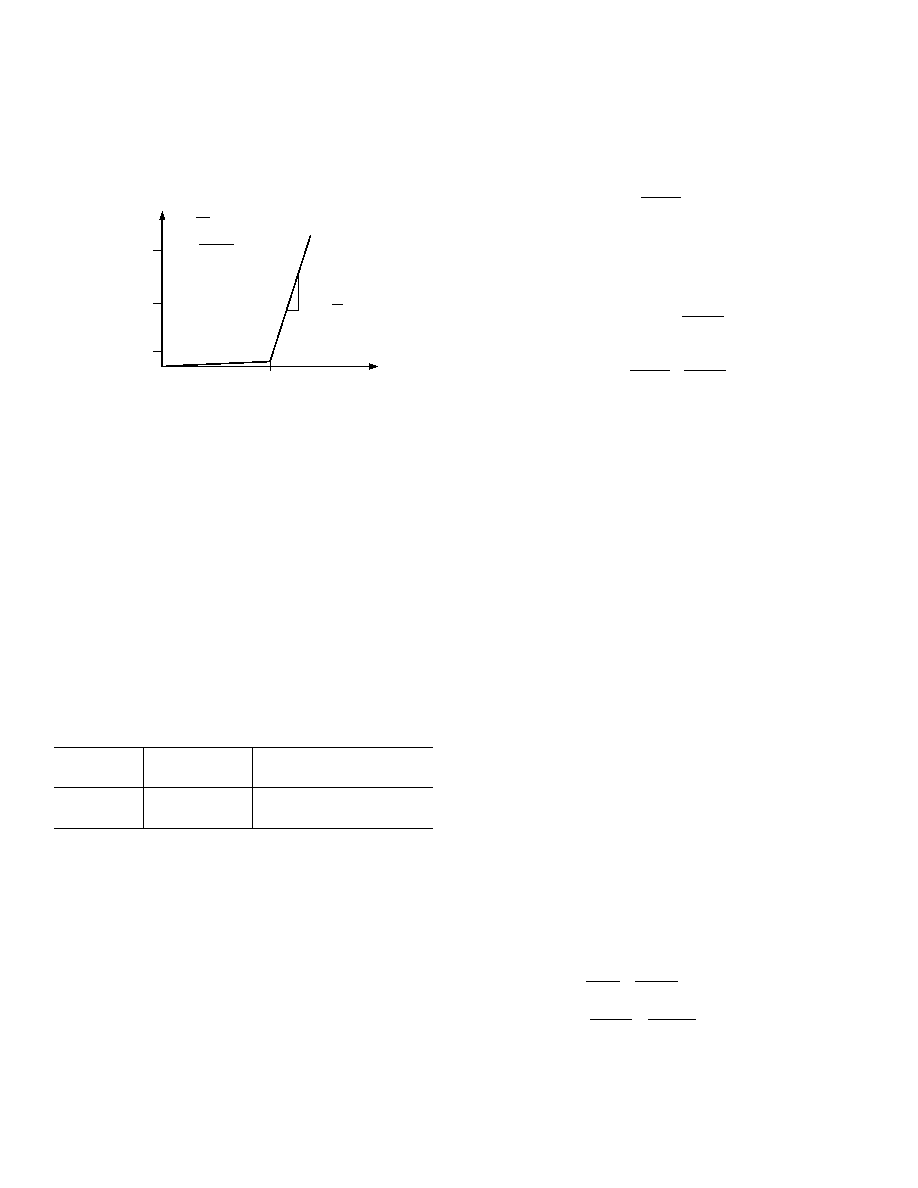
GENERAL
Laser diodes have current-in to light-out transfer functions as
shown in Figure 1. Two key characteristics of this transfer function
are the threshold current, I
TH
, and slope in the linear region
beyond the threshold current, referred to as the slope efficiency, LI.
ER = P1
P0
2
I
TH
CURRENT
O
PTICAL POWER
P0
P1
P
AV
P
I
I
LI =
P
P
AV
= P1 + P0
Figure 1. Laser Transfer Function
CONTROL
A monitor photodiode, MPD, is required to control the LD. The
MPD current is fed into the ADN2843 to control the power
and extinction ratio, continuously adjusting the bias current and
modulation current in response to the laser's changing threshold
current and light-to-current slope efficiency.
The ADN2843 uses automatic power control, APC, to maintain
a constant average power over time and temperature.
The ADN2843 uses closed-loop extinction ratio control to allow
optimum setting of the extinction ratio for every device. Thus,
SONET/SDH interface standards can be met over device variation,
temperature, and laser aging. Closed-loop modulation control
eliminates the need to either overmodulate the LD or include
external components for temperature compensation, thus reducing
research and development time and second sourcing issues.
The ADN2843 dual-loop control has two modes of operation.
Each mode is given by the configuration of the MODE and
D_IMOD pins as shown below.
Operation
MODE
D_IMOD
Mode
Pin Setting
Pin Connected to
A
HIGH
IBIAS
B
LOW
IBIAS_CTRL
Configuring the ADN2843 in Mode A or Mode B (see Figures 3
and 4) enables users to achieve accurate control of the extinc-
tion ratio. Mode B is suitable for applications where an IBIAS
pin is not available to the TOSA, or where there is no space
on the TOSA for an IBIAS inductor. Experimental data and
simulation for typical lasers has shown ER to be 0.3 dB to 0.5 dB
better in Mode A, at a 5 dB extinction ratio. Care should be
taken to ensure that the extra capacitance on the I
BIAS
pin
due to the D_IMOD connection does not degrade the eye
quality. When physical constraints do not allow a low capaci-
tance interconnect between D_IMOD and I
BIAS
, the ADN2843
should be configured in Mode B (see Figure 4).
Average power and extinction ratio for both modes are set using
the PSET and ERSET pins, respectively. Potentiometers are
connected between these pins and ground. The potentiometer
R
PSET
is used to set the average power. The potentiometer R
ERSET
is used to set the extinction ratio. The internal control loops
force the PSET and ERSET pins to 1.23 V above GND. For
initial setup, R
PSET
and R
ERSET
may be calculated using the
following formulas:
The PSET resistor is given by the following formulas:
R
V
I
PSET
AV
=
( )
1 23
.
W
where I
AV
is average MPD current.
The value of the ERSET resistor is a function of the operation
mode of the ADN2843 as follows:
For Mode A:
R
R
ER
ER
ERSET
PSET
=
•
+ 1
1
≠
For Mode B:
R
R
ER
ER
ERSET
PSET
=
•
+
2
1
1
≠
Note that I
ERSET
and I
PSET
will change from laser diode to laser
diode, therefore R
ERSET
and R
PSET
need to be adjusted for each
laser diode. When tuning the laser diode, R
PSET
should be
adjusted first with R
ERSET
at 25 k . Once the average power is
set, R
ERSET
is adjusted to set the desired extinction ratio, and
R
PSET
is again adjusted to re-establish the desired average power.
Once the values R
PSET
and R
ERSET
have been adjusted to set the
desired average power and extinction ratio, the control loops
maintain these values of average power and extinction ratio over
environmental conditions and time.
PAVCAP AND ERCAP
The control loop constants are set by the PAVCAP and ERCAP
capacitors. The required value for the PAVCAP and ERCAP
capacitors is 22 nF.
The PAVCAP and ERCAP capacitors are connected between
the respective pins and GND. The capacitors should be low
leakage multilayer ceramic capacitors with an insulation resistance
>100 G or an RC >1000 s, whichever is lowest.
ALARMS
The ADN2843 is designed to allow interface compliance to
ITU-T-G958 (11/94), Section 10.3.1.1.2 (Transmitter Fail),
and Section 10.3.1.1.3 (transmitter degrade). The ADN2843
has two alarms, DEGRADE and FAIL. These alarms are raised
when I
BIAS
exceeds the respective DEGRADE and FAIL thresh-
olds. These alarms are active high. A resistor between ground
and the ASET pin is used to set the current at which these
alarms are raised. The current through the ASET resistor is a
ratio of 1:100 to the FAIL alarm threshold. The DEGRADE
alarm will be raised at 90% of the FAIL threshold.
Example:
I
mA so I
mA
I
I
mA
A
R
V
I
V
A
k
FAIL
DEGRADE
ASET
FAIL
ASET
ASET
=
=
=
=
=
=
=
=
50
45
100
50
100
500
1 23
1 23
500
2 46
.
.
.
W
The laser degrade alarm, DEGRADE, is provided to give a warn-
ing of imminent laser failure if the laser diode degrades further or
if environmental conditions continue to stress the LD, such as
increasing temperature.
REV. 0
ADN2843
≠7≠
The laser fail alarm, FAIL, is activated when the transmitter can
no longer be guaranteed to be SONET/SDH compliant. This
occurs when one of the following conditions arise:
The ASET threshold is reached.
The ALS pin is set high. This shuts off the modulation and
bias currents to the LD, resulting in the MPD current
dropping to zero. This gives closed-loop feedback to the
system that ALS has been enabled.
DEGRADE is raised only when the bias current exceeds
90% of the alarm threshold.
ALARM INTERFACE
The alarm voltages are open collector outputs. An internal
pull-up resistor of 30k that is used to pull the logic high
value to V
CC
. However, this can be overdriven with an external
resistor, allowing alarm interfacing to non-V
CC
levels. The
FAIL output may not be connected directly to the ALS pin to
shut down the bias and modulation currents. It can however
be latched using a flip-flop, and the output of the flip-flop can
then be used to activate ALS. Non-V
CC
alarm output levels
must be below the V
CC
used for the ADN2843.
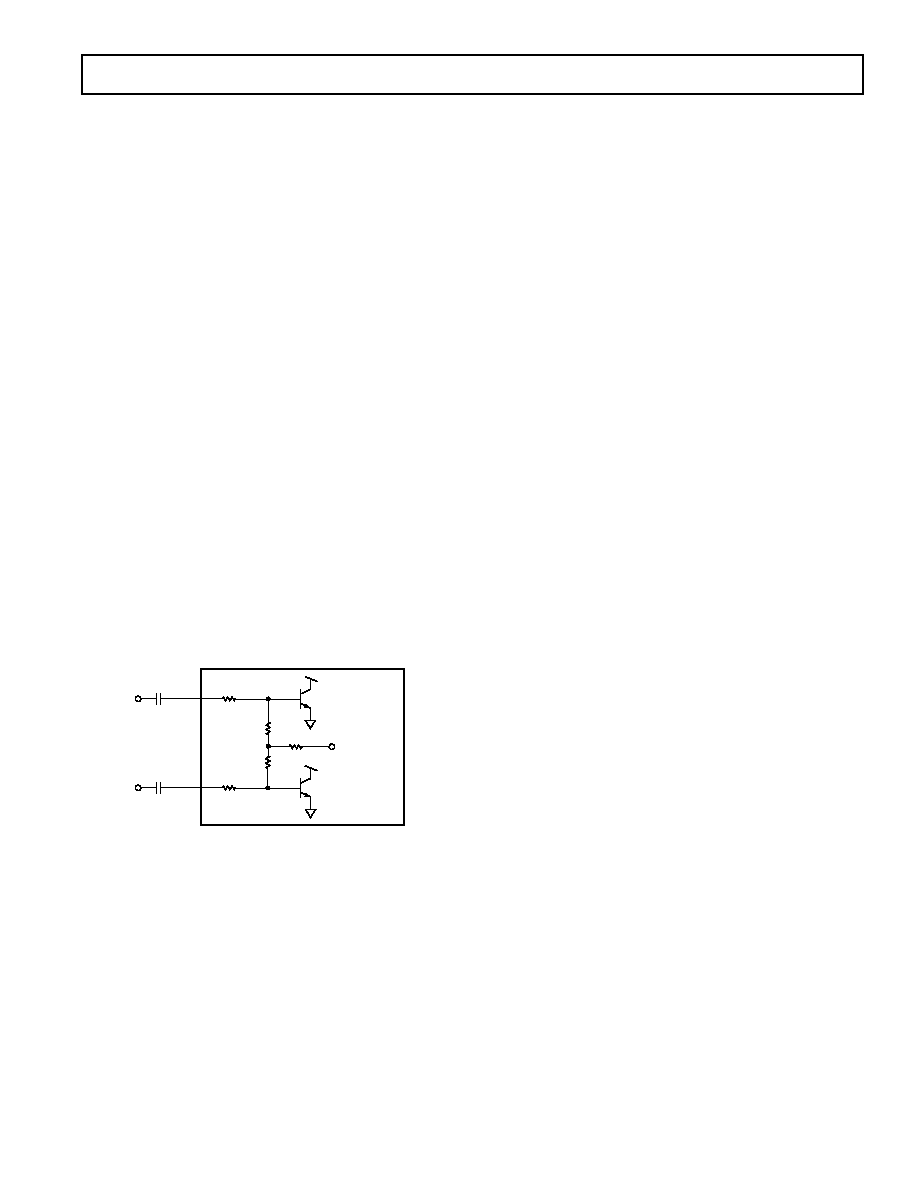
DATA INPUTS
Figure 2 shows a simplified schematic of the ADN2845 data
inputs. The data inputs are terminated via the equivalent of a
100 internal resistor between DATAN and DATAP. This
provides 50 termination for single-ended signals. The actual
signal on the switching devices is attenuated by a factor of 2
internally. There is a high impedance circuit to set the common-
mode voltage, which is designed to change over temperature. It
is recommended that ac coupling be used to eliminate the need
for matching between the common-mode voltages.
25
25
25
25
2k
INTERNAL
REFERENCE
ADN2845
DATAN
DATAP
Figure 2. Simplified Schematic of Data Inputs
MONITOR CURRENTS
IBMON, IMMON mirror the bias, modulation current at a ratio
of 1:100 for increased monitoring functionality. IMPDMON and
IMPDMON2 mirror the current in IMPD and IMPD2, respec-
tively, with a ratio of 1. All monitors source current from V
CC
.
If the MPD monitoring function is not required, then the IMPD
pin should be tied to ground and the monitor photodiode cathode
should be connected directly to the PSET pin. When the MPD
monitor functions are not used, IMPDMON and IMPDMON2
should be tied to V
CC
.
MPD CURRENT
The maximum average MPD current is specified in the specifica-
tions section. This maximum current specified is limited by the
MPD monitoring circuitry. If the monitoring function is not
required, then IMPD and IMPD2 should be grounded, the moni-
tor photodiode cathode should be connected directly to the PSET
node, and IMPDMON and IMPDMON2 should be tied to V
CC
.
MPD currents as high as 3 mA can be used in this configuration.
Another way to increase the MPD current range without sacri-
ficing the monitoring function is to use IMPD and IMPD2 in
parallel. This effectively doubles the current range but raises the
lower MPD current specification from 50 A to 100 A. If this
configuration is used, the IMPDMON and IMPDMON2 pins
should be tied together and terminated with a single resistor.
The mirror ratio of 1 is maintained in this configuration.
DUAL MPD DWDM FUNCTION
The MPD function mirrors the current in MPD to the PSET pin
and to the IMPDMON pin with a ratio of 1. A second monitor
photodiode can be connected to the IMPD2 pin. Its current is
mirrored to IMPDMON2 and also to the PSET pin, where it is
summed with the current mirrored from IMPD. The two MPD
monitor currents can be used as inputs to a DWDM wavelength
control function when used in combination with various optical
filtering techniques. If the IMPD monitor function is not required,
the monitor photodiode can be directly connected to the PSET
pin, and the IMPD pin must be tied to GND. If the IMPD2 pin
is not being used, it should be tied to GND.
IDTONE
The IDTONE pin is supplied for fiber identification/supervisory
channels or for control purposes. This pin modulates the optical
one level by adding a current to IMOD over a possible range of
2% of minimum I
MOD
to 10% of maximum I
MOD
. The IDTONE
current is set by an external current sink connected to the
IDTONE pin. There is a gain of 2 between the IDTONE pin
and the I
MOD
current. To ratio the IDTONE current to I
MOD
, the
input current can be derived from the IMMON output current.
If the IDTONE function is not being used, this pin must be tied
to V
CC
to properly disable it.
Note that using IDTONE during transmission may cause optical
eye degradation.
AUTOMATIC LASER SHUTDOWN (ALS)
The ADN2843 ALS allows compliance to ITU-T-G958 (11/94),
Section 9.7. When ALS is asserted, both bias and modulation
currents are turned off. In ALS mode, current is sourced to the
laser from the I
BIAS
pin, which reverse biases the laser and ensures
that it is turned off. Correct operation of ALS can be confirmed
by the FAIL alarm being raised when ALS is asserted. Note this
is the only time that DEGRADE will be low while FAIL is high.
Note that for correct ALS operation, the ALS pin on the
ADN2845 and ADN2844 should be connected and termi-
nated with a 10 k
W resistor. The ADN2843 ALS should be
driven with correct logic levels (see Specifications section). ALS
should never be left floating.
POWER DISSIPATION
The power dissipation of the ADN2845 can be calculated using
the following expressions:
I
mA
I
mA
I
mA
P
V
I
A
V
I
A
V
I
A
CC
MOD
BIAS
CC
CC
IMOD
MOD
IBIAS
BIAS
=
+
•
( )
+
•
( )
=
•
( )
+
•
( )
+
•
( )
75
1 75
0 3
2
.
.
/
where V
IMOD
is the average voltage on the IMOD pin, and
V
IBIAS
is the average voltage on the I
BIAS
pin.
REV. 0
≠8≠
ADN2843
∑ Best high frequency board layout techniques including power and ground planes should be used.
∑ To minimize inductance, keep the connections between the ADN2845 and the laser diode as short as possible. Inductances <0.3 nH
are recommended for best performance. Critical bonds are IMODP and V
CC
(Pin 14). Ribbon bonding can be used to reduce
bond inductance. Minimize bond lengths for ADN2845 pads to achieve low inductance.
∑ Place bypass capacitor on laser anode as close to laser as possible.
∑ Bypass capacitors should be placed as close as possible to V
CC
pads.
∑ 50 controlled impedance interconnects should be used on the DATA inputs.
∑ Parasitic capacitance on IBIAS_CTRL and IMOD_CTRL interconnects should be less than 100 pF. If decoupling caps are used
on IBIAS_CTRL and IMOD_CTRL, they should be tied to V
CC
rather than GND.
∑ An inductor should be used in the bias current path. A Microwave Components coil 30-1847-GCCAS-01 (48 mil
24 mil) should
be used.
∑ The recommended substrate connection is to GND. However, the performance is not affected by connecting the substrate to V
CC.
22nF
10nF
GND
GND
ERCAP
PAVCAP
MODE
GND
GND
GND
V
CC
D_IMOD
IMOD_CTRL
GND
IBIAS_CTRL
IDTONE
IBMON
IMMON
ALS
FAIL
DEGRADE
GND
ASET
ERSET
PSET
GND
IMPD
IMPDMON
IMPDMON2
ADN2844
GND
1
8
32 25
IMPD2
GND
DATAN
GND
NC
GND
DATAP
IMODNTERM
NC
IMODP
IBIAS
ALS
GND
V
CC
V
CC
V
CC
GND
ADN2845
IMOD_CTRL
IBIAS_CTRL
15
18
9
6
1
10
14
5
10nF
10k
1k
1k
22nF
GND
V
CC
24
17
9 16
V
CC
10nF
10nF
100 F TANTALUM
V
CC
10nF
V
CC
MPD
10nF
V
CC
V
CC
10nF
V
CC
NOTES
*FOR DIGITAL PROGRAMMING, THE ADN2850 OR ADN2860 OPTICAL SUPERVISOR CAN BE USED.
**OPTIONAL MONITORING OF CURRENTS.
1k
NC
*
*
**
**
**
V
CC
V
CC
V
CC
V
CC
V
CC
Figure 3. ADN2843 Application Circuit (Mode A)
REV. 0
ADN2843
≠9≠
GND
GND
ERCAP
PAVCAP
MODE
GND
GND
LBWSET
D_IMOD
IMOD_CTRL
GND
IBIAS_CTRL
IDTONE
IBMON
IMMON
ALS
FAIL
DEGRADE
GND
ASET
ERSET
PSET
GND
IMPD
IMPDMON
IMPDMON2
ADN2844
GND
1
8
32 25
IMPD2
GND
DATAN
GND
NC
NC
GND
DATAP
IMODNTERM
IMODP
ALS
GND
GND
ADN2845
IMOD_CTRL
IBIAS_CTRL
15
18
9
6
1
10
14
5
GND
V
CC
24
17
9 16
100 F TANTALUM
MPD
10nF
GND
IBIAS
22nF
10nF
V
CC
10nF
10k
1k
1k
22nF
V
CC
10nF
10nF
V
CC
10nF
V
CC
10nF
V
CC
V
CC
V
CC
V
CC
1k
V
CC
V
CC
V
CC
NOTES
*FOR DIGITAL PROGRAMMING, THE ADN2850 OR ADN2860 OPTICAL SUPERVISOR CAN BE USED.
**OPTIONAL MONITORING OF CURRENTS.
*
*
**
**
**
V
CC
V
CC
V
CC
V
CC
Figure 4. ADN2843 Application Circuit (Mode B)
REV. 0
≠10≠
ADN2843
Figure 5. Recommended Layout
GROUND PLANE
PARALLEL PLATE
DECOUPLING
CAPACITOR
NOTES
∑ FOR OPTIMUM PERFORMANCE, RIBBON BONDS ARE RECOMMENDED ON PADS 1, 5, 12, AND 14. WIRES ARE 3 MIL OR 5 MIL RIBBONS <400 m
∑
LONG. ALL OTHER PINS CAN BE ROUND WIRE <1mm.
∑ LASER'S ANODE IS CONNECTED TO V
CC
THROUGH GOLD LAYER ON TOP OF CERAMIC STANDOFF. STANDOFF MINIMIZES LENGTH OF PAD
∑
12 AND PAD 14 RIBBONS.
∑ PARALLEL PLATE DECOUPLING CAPACITORS SHOULD BE >100pF AND BE OF MICROWAVE AVX TYPE, PART NO. GB0159391KA6N (390pF).
∑ THE RECOMMENDED SUBSTRATE CONNECTION IS TO GND. HOWEVER, PERFORMANCE IS NOT AFFECTED BY CONNECTING THE
∑
SUBSTRATE TO VCC.
∑ AN INDUCTOR SHOULD BE USED IN THE BIAS CURRENT PATH. A MICROWAVE COMPONENTS COIL 30-1847-GCCAS-01 (48 MIL 24 MIL)
SHOULD BE USED.
∑ THE EXTERNAL POWER SUPPLY IS CONNECTED AT THE PARALLEL PLATE DECOUPLING CAPACITOR.
MPD
50 TRANSMISSION LINE
GROUND PLANE
IBIAS OUTPUT INDUCTOR
LASER LIGHT
LASER
CERAMIC WITH GOLD
SURFACE THAT CONTACTS
THE LASER'S ANODE
PARALLEL PLATE
DECOUPLING
CAPACITORS
BACK FACET LIGHT
ADN2845
18
15
14
10
9
6
5
1
AGND
V
CC
V
CC
V
CC
V
CC
IMODP
IBIAS
AGND
ALS IMOD_CTRL IBIAS_CTRL
AGND
DATAP
AGND
DATAN
IMODNTERM
Figure 6. 10 Gbps Optical Diagram Provided Courtesy of NEL.
P
AV
= 0 dBm, ER = 5 dB, PRBS 31 Pattern.

REV. 0
ADN2843
≠11≠
DIE PAD COORDINATES
(With Origin in the Center of the Die)
ADN2844
Pad Number
Pad Name
X ( m)
Y ( m)
1
ASET
1014.00
≠1019.00
2
ERSET
769.00
≠1019.00
3
PSET
486.00
≠1019.00
4
GND
186.00
≠1019.00
5
IMPD
≠132.00
≠1019.00
6
IMPDMON
≠479.00
≠1019.00
7
IMPDMON2
≠811.00
≠1019.00
8
IMPD2
≠1056.00
≠1019.00
9
GND
≠1339.00
≠877.00
10
V
CC
≠1339.00
≠672.00
11
ERCAP
≠1339.00
≠429.00
12
PAVCAP
≠1339.00
≠204.00
13
MODE
≠1339.00
91.00
14
GND
≠1339.00
335.00
15
GND
≠1339.00
580.00
16
GND
≠1339.00
824.00
17
GND
≠1051.00
1019.00
18
GND
≠761.00
1019.00
19
DEGRADE
≠476.00
1019.00
20
FAIL
≠207.00
1019.00
21
ALS
102.00
1019.00
22
IMMON
387.00
1019.00
23
IBMON
653.00
1019.00
24
IDTONE
904.00
1019.00
25
GND
1359.00
995.00
26
V
CC
1359.00
781.00
27
IBIAS_CNTRL
1359.00
523.00
28
GND
1359.00
317.00
29
IMOD_CTRL
1359.00
≠29.00
30
D_IMOD
1359.00
≠294.00
31
GND
1359.00
≠562.00
32
GND
1359.00
≠807.00
ADN2845
Pad Number
Pad Name
X ( m)
Y ( m)
1
DATAN
≠500.00
400.00
2
GND
*
≠500.00
222.00
3
NC
≠500.00
0.00
4
GND
*
≠500.00
≠222.00
5
DATAP
≠500.00
≠400.00
6
ALS
≠300.00
≠600.00
7
IMOD_CTRL
≠100.00
≠600.00
8
IBIAS_CTRL
100.00
≠600.00
9
GND
*
300.00
≠600.00
10
NC
*
500.00
≠400.00
11
IBIAS
500.00
≠200.00
12
IMODP
*
500.00
≠30.00
13
NC
*
500.00
178.00
14
V
CC
(IMODN)
*
500.00
378.00
15
GND
*
300.00
600.00
16
V
CC
*
100.00
600.00
17
V
CC
*
≠100.00
600.00
18
V
CC
*
≠300.00
600.00
*
Denotes double bond pad.
REV. 0
C02764≠0≠4/03(0)
≠12≠
ADN2843
OUTLINE DIMENSIONS
32-Lead Lead Frame Chip Scale Package [LFCSP]
5 mm 5 mm
(CP-32)
Dimensions shown in millimeters
COMPLIANT TO JEDEC STANDARDS MO-220-VHHD-2
0.30
0.23
0.18
0.20 REF
0.80 MAX
0.65 NOM
0.05 MAX
0.02 NOM
12
MAX
1.00
0.90
0.80
SEATING
PLANE
COPLANARITY
0.08
1
32
8
9
25
24
16
17
BOTTOM
VIEW
0.50
0.40
0.30
3.50
REF
0.50
BSC
PIN 1
INDICATOR
TOP
VIEW
5.00
BSC SQ
4.75
BSC SQ
SQ
3.25
3.10
2.95
PIN 1
INDICATOR
0.60 MAX
0.60 MAX
Exposed paddle should be soldered to the most negative supply of the ADN284
(ADN2844 also available as bare die)